OPTICAL FIBER COMMUNICATION - Ernasugesti's Blog · Relates effects of fiber attenuation and fiber...
54
OPTICAL FIBER COMMUNICATION • Digital Receivers • Probability of error • Quantum Limit • Shot noise • Noise Penalty • Pre-amplifier types PART III:- DIGITAL RECEIVERS
Transcript of OPTICAL FIBER COMMUNICATION - Ernasugesti's Blog · Relates effects of fiber attenuation and fiber...
OPTICAL FIBER
COMMUNICATION
• Digital Receivers
• Probability of error
• Quantum Limit
• Shot noise
• Noise Penalty
• Pre-amplifier types
PART III:-
DIGITAL RECEIVERS
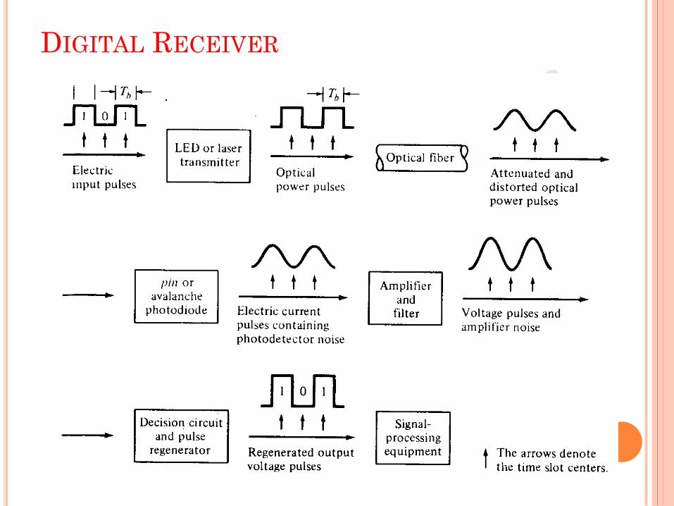
DIGITAL RECEIVER

DIGITAL RECEIVER
• Analog system—Signal to rms noise ratio
• Digital system– Average error probability

DIGITAL RECEIVER-
PHOTON DETECTION QUANTUM NOISE
• Due to random arrival rate of signal photons. • Makes primary photocurrent a time varying Poisson Process. • If detector illuminated by optical signal p(t), then average number of electron-hole pair generated in time τ is --
• η is detector quantum efficiency.

DIGITAL RECEIVER-
PHOTON DETECTION QUANTUM NOISE
• Actual number of electron-hole pair n fluctuates from average according to Poisson distribution.
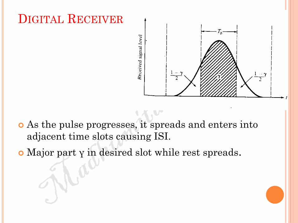
DIGITAL RECEIVER
As the pulse progresses, it spreads and enters into
adjacent time slots causing ISI.
Major part γ in desired slot while rest spreads.
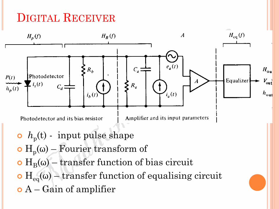
DIGITAL RECEIVER
hp(t) - input pulse shape
Hp(ω) – Fourier transform of
HB(ω) – transfer function of bias circuit
Heq(ω) – transfer function of equalising circuit
A – Gain of amplifier

DIGITAL RECEIVER
η – Quantum efficiency of photo detector
Cd – Photodiode capacitance
Rb – Detector bias resistance
Ra ІІ Ca – Amplifier input impedance
Ca – Amplifier shunt capacitance
ib(t) – Thermal noise current generated by Rb
ia(t) – Thermal noise current generated by Ra
va(t) – Thermal noise voltage of amplifier channel
Input voltage develops across Ra
Two amplifier noise sources ia(t) , va(t)
One detector noise source ib(t) due to bias resistor.
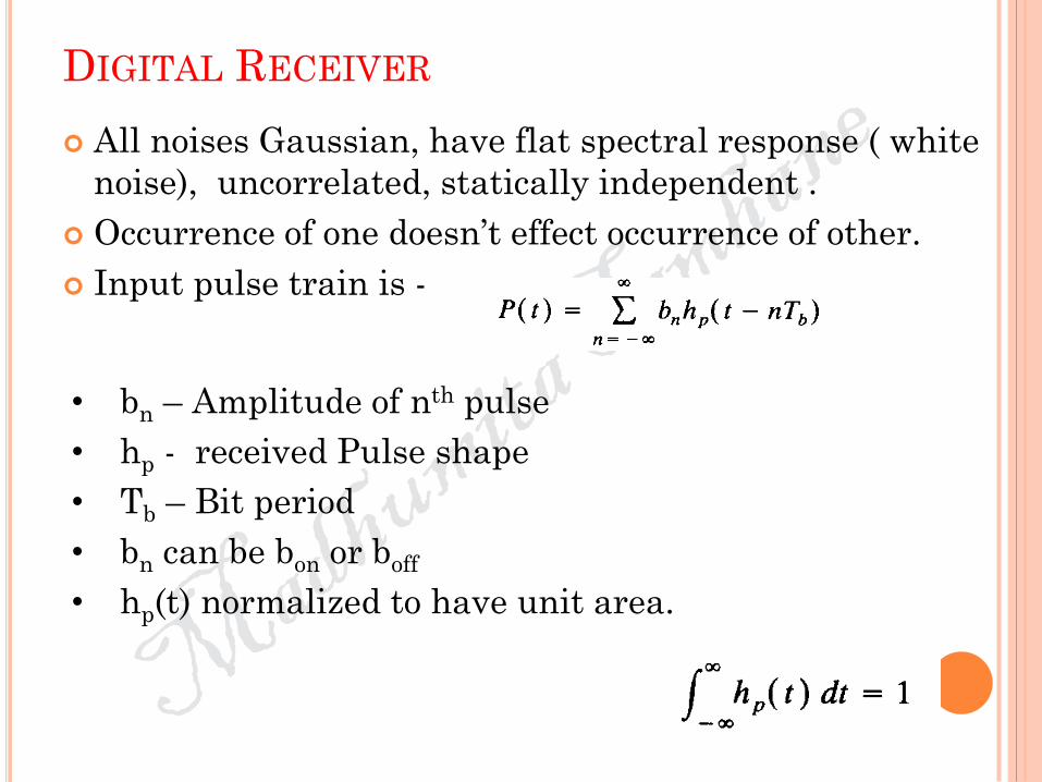
DIGITAL RECEIVER
All noises Gaussian, have flat spectral response ( white
noise), uncorrelated, statically independent .
Occurrence of one doesn’t effect occurrence of other.
Input pulse train is -
• bn – Amplitude of nth pulse
• hp - received Pulse shape
• Tb – Bit period
• bn can be bon or boff
• hp(t) normalized to have unit area.
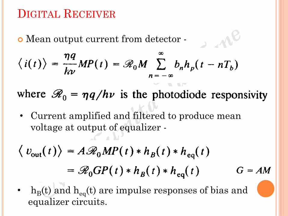
DIGITAL RECEIVER
Mean output current from detector -
• Current amplified and filtered to produce mean
voltage at output of equalizer -
• hB(t) and heq(t) are impulse responses of bias and
equalizer circuits.
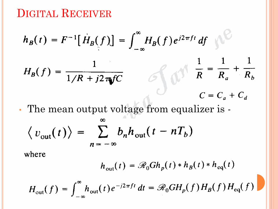
DIGITAL RECEIVER
• The mean output voltage from equalizer is -
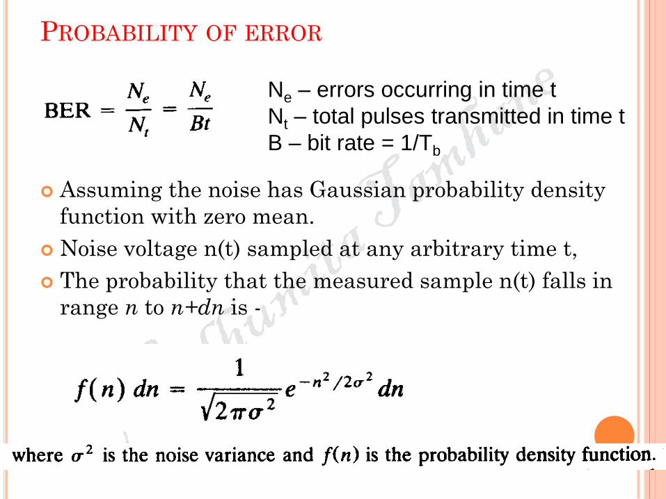
PROBABILITY OF ERROR
Ne – errors occurring in time t
Nt – total pulses transmitted in time t
B – bit rate = 1/Tb
Assuming the noise has Gaussian probability density
function with zero mean.
Noise voltage n(t) sampled at any arbitrary time t,
The probability that the measured sample n(t) falls in
range n to n+dn is -
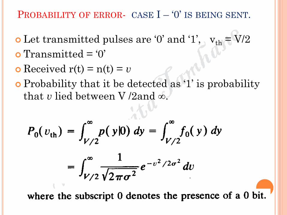
PROBABILITY OF ERROR- CASE I – ‘0’ IS BEING SENT.
Let transmitted pulses are ‘0’ and ‘1’, vth = V/2
Transmitted = ‘0’
Received r(t) = n(t) = v
Probability that it be detected as ‘1’ is probability
that v lied between V /2and ∞.

PROBABILITY OF ERROR- CASE II – ‘1’ IS BEING SENT.
Transmitted = ‘1’
Received r(t) = V + n(t) = v
n(t) = v - V
Probability that it be detected as ‘0’ is probability that
v lied between - ∞and V /2.

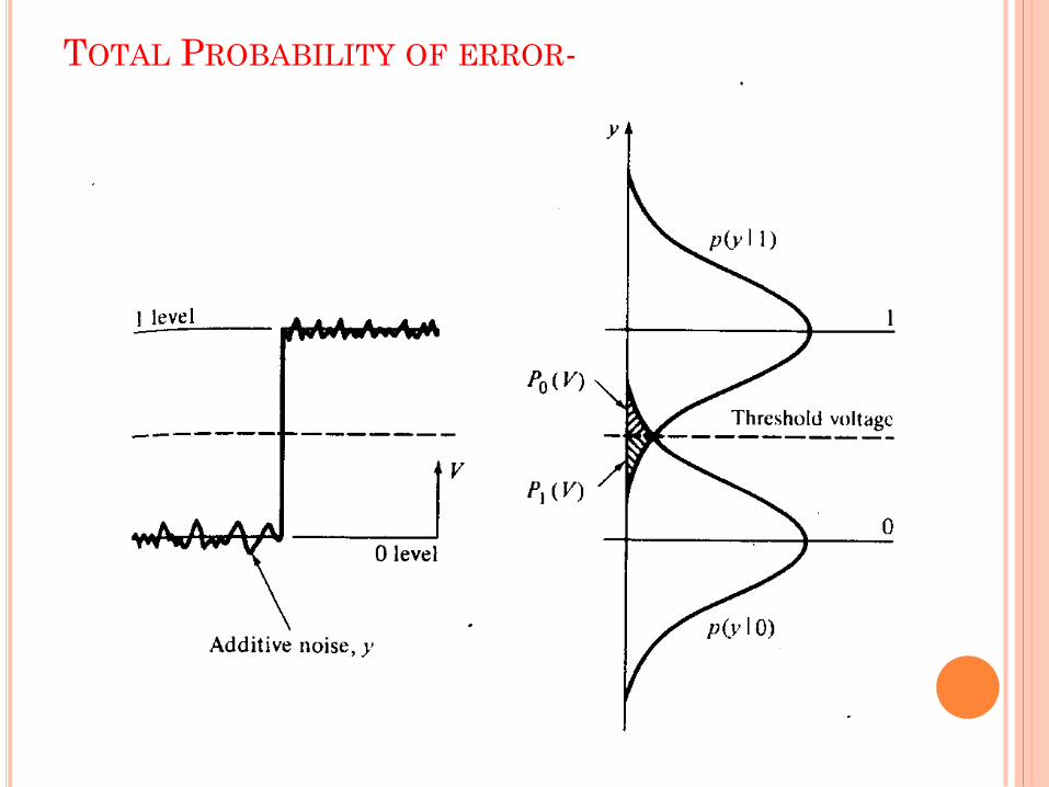
TOTAL PROBABILITY OF ERROR-
Pe = a p0(v) + b p1(v)
Assuming ‘0’ and ‘1’ are equiprobable, a = b = 0.5.
Pe = ?
Looking at distribution p0(v) and p1(v) are identical.
Integrating double of one part -
TOTAL PROBABILITY OF ERROR-
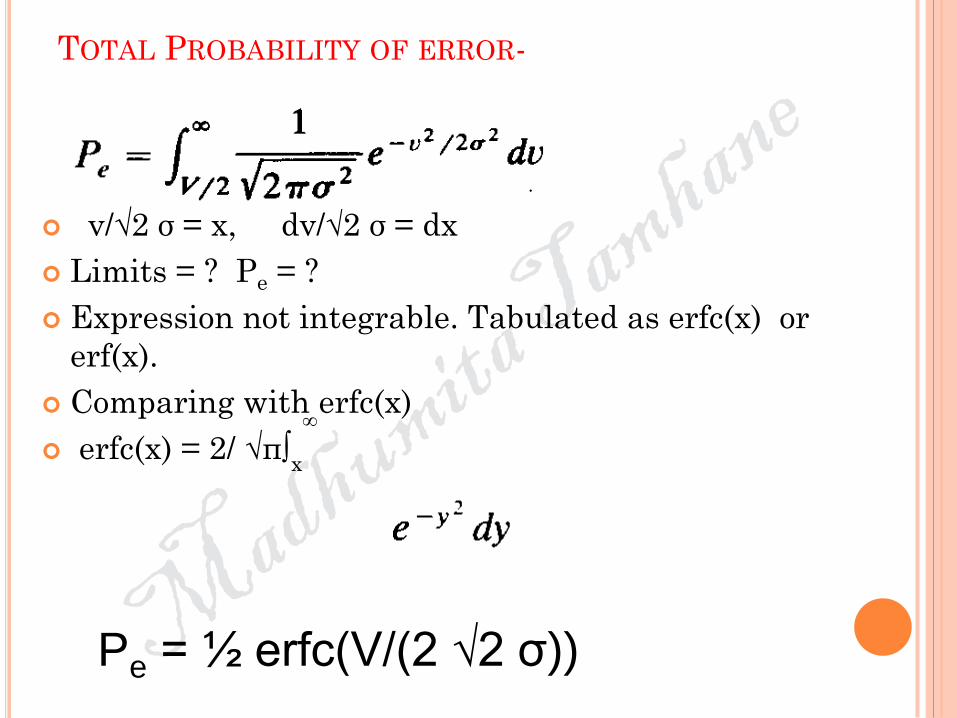
TOTAL PROBABILITY OF ERROR-
v/√2 σ = x, dv/√2 σ = dx
Limits = ? Pe = ?
Expression not integrable. Tabulated as erfc(x) or
erf(x).
Comparing with erfc(x)
erfc(x) = 2/ √π∫x
∞
Pe = ½ erfc(V/(2 √2 σ))
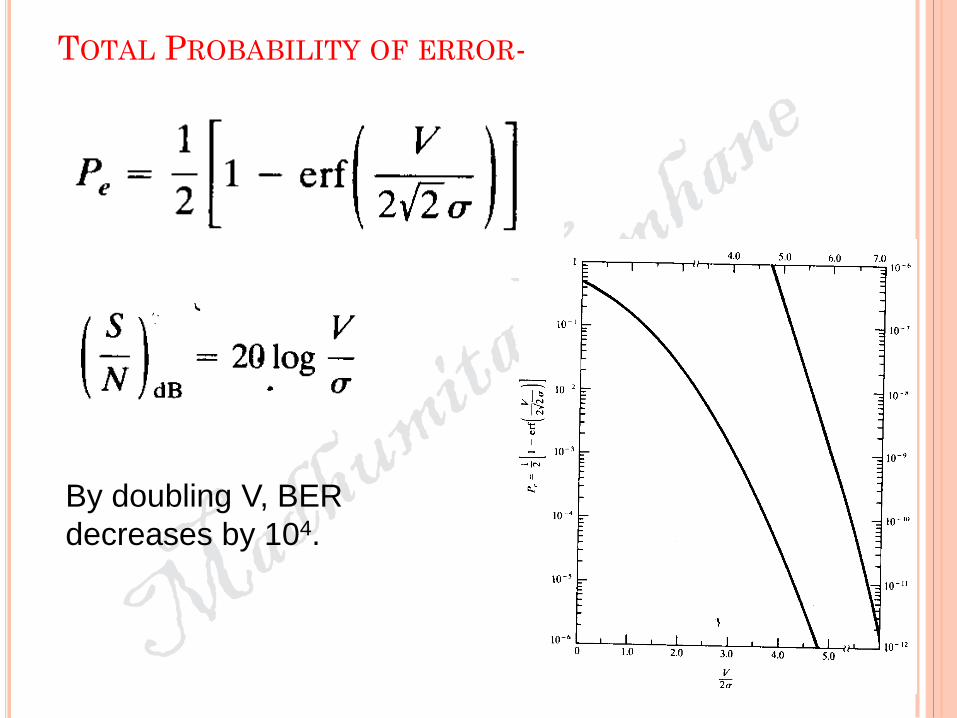
TOTAL PROBABILITY OF ERROR-
By doubling V, BER
decreases by 104.
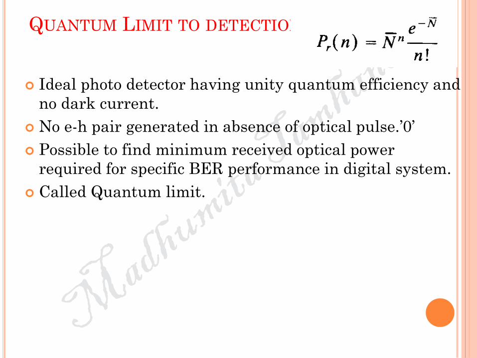
QUANTUM LIMIT TO DETECTION
Ideal photo detector having unity quantum efficiency and
no dark current.
No e-h pair generated in absence of optical pulse.’0’
Possible to find minimum received optical power
required for specific BER performance in digital system.
Called Quantum limit.
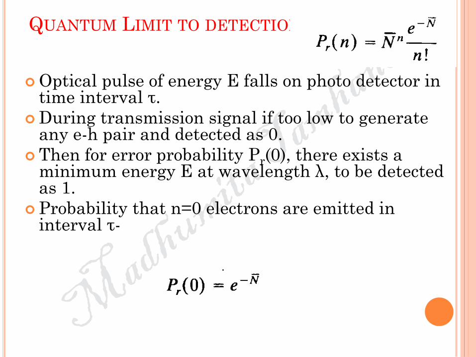
QUANTUM LIMIT TO DETECTION
Optical pulse of energy E falls on photo detector in time interval τ.
During transmission signal if too low to generate any e-h pair and detected as 0.
Then for error probability Pr(0), there exists a minimum energy E at wavelength λ, to be detected as 1.
Probability that n=0 electrons are emitted in interval τ-
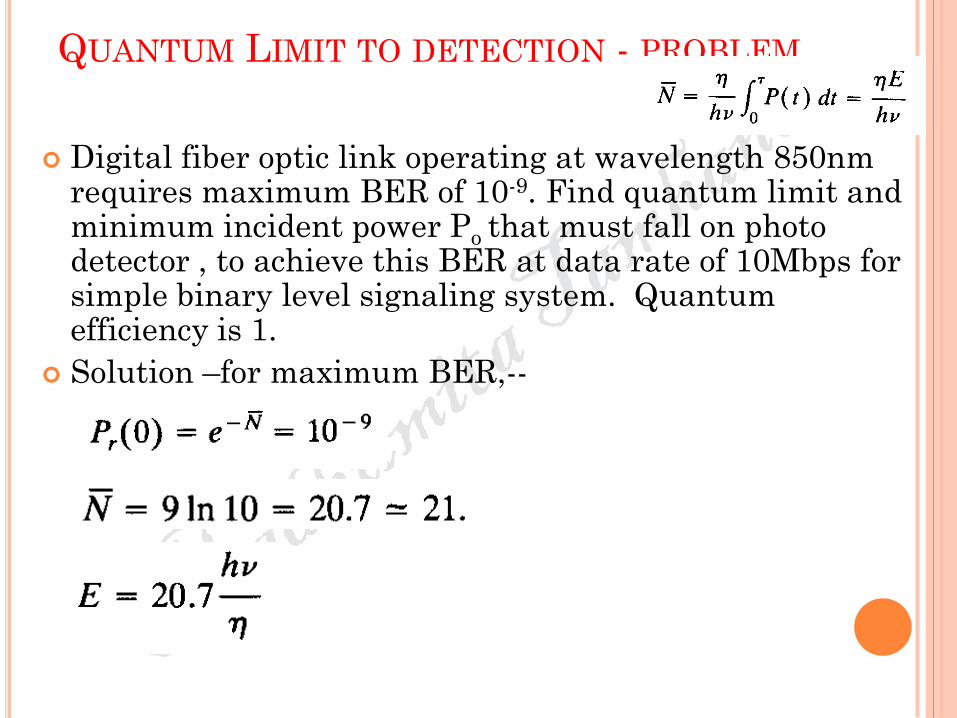
QUANTUM LIMIT TO DETECTION - PROBLEM
Digital fiber optic link operating at wavelength 850nm requires maximum BER of 10-9. Find quantum limit and minimum incident power Po that must fall on photo detector , to achieve this BER at data rate of 10Mbps for simple binary level signaling system. Quantum efficiency is 1.
Solution –for maximum BER,--

QUANTUM LIMIT TO DETECTION - PROBLEM
Minimum incident power that must fall on photo
detector Po --- E= Po τ
Assuming equal number of 0 and 1, 1/ τ = B/2

RECEIVER NOISES
Noise voltage vN(t) causes vout to deviate from
mean or average < vout >
• vs(t) – Quantum or shot noise due to random
multiplied poisson nature of photocurrent is(t).
• vR(t) – thermal noise due to bias resistor Rb.
• vI(t) –noise due to amplifier input noise
• vE(t) –noise due to amplifier due to ea(t).
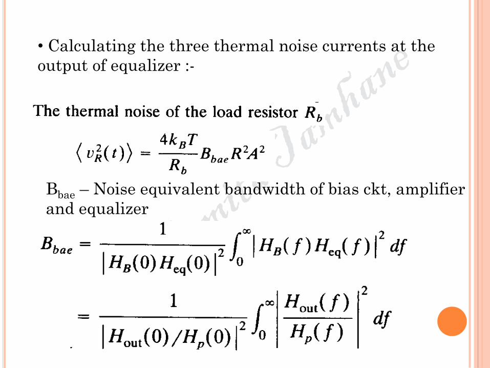
Bbae – Noise equivalent bandwidth of bias ckt, amplifier
and equalizer
• Calculating the three thermal noise currents at the
output of equalizer :-


SHOT NOISES-
•Shot noise in bit period Tb is shot noise contribution from
a pulse within that period as well as from all other pulses
outside that period.
•Worst case shot noise when all neighboring pulses are ‘1’.
•Greatest ISI.
•Hence mean unity gain photocurrent over Tb for 1 pulse -

SHOT NOISES – ‘1’ WITH ALL NEIGHBOR ‘1’S
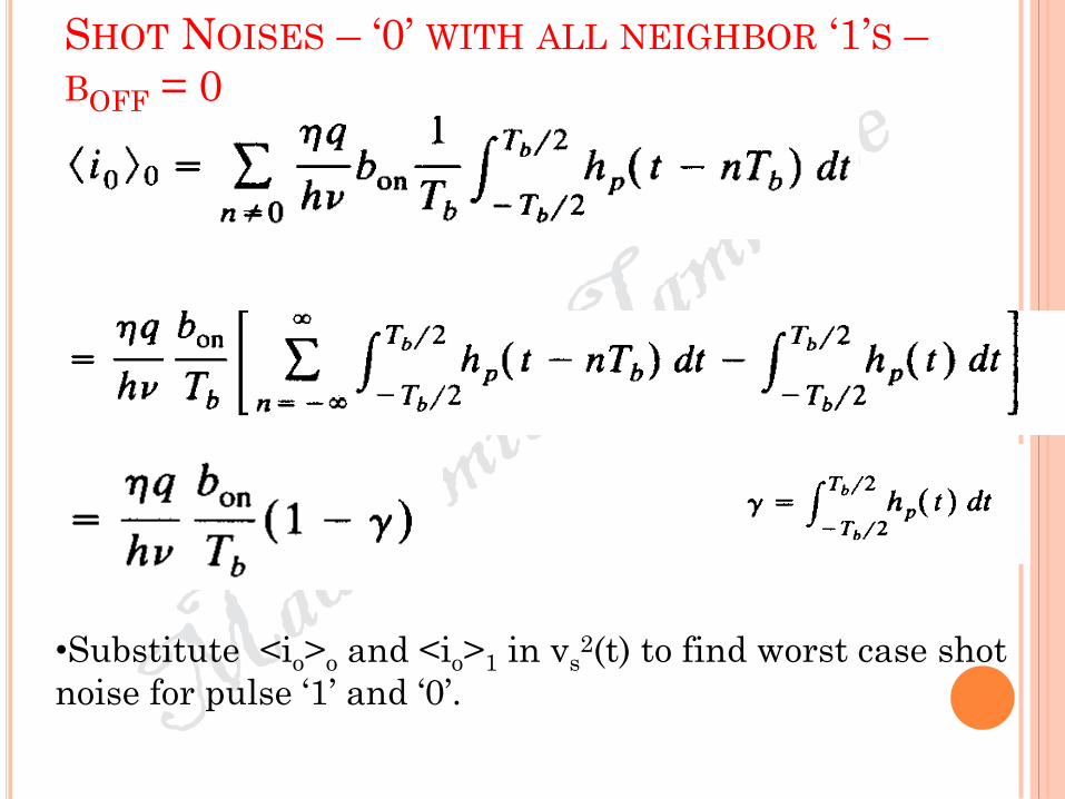
SHOT NOISES – ‘0’ WITH ALL NEIGHBOR ‘1’S –
BOFF = 0
•Substitute <io>o and <io>1 in vs2(t) to find worst case shot
noise for pulse ‘1’ and ‘0’.
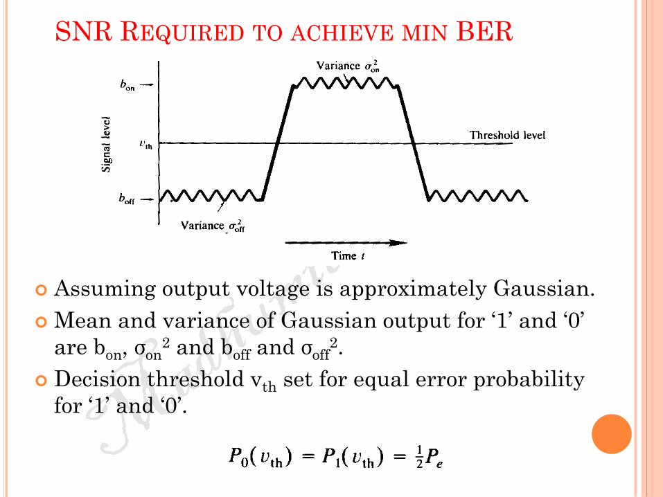
SNR REQUIRED TO ACHIEVE MIN BER
Assuming output voltage is approximately Gaussian.
Mean and variance of Gaussian output for ‘1’ and ‘0’
are bon, σon2 and boff and σoff
2.
Decision threshold vth set for equal error probability
for ‘1’ and ‘0’.
SNR REQUIRED TO ACHIEVE MIN BER
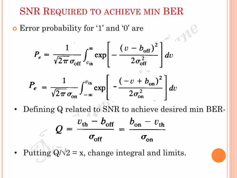
Error probability for ‘1’ and ‘0’ are
-
• Defining Q related to SNR to achieve desired min BER-
• Putting Q/√2 = x, change integral and limits.

SNR REQUIRED TO ACHIEVE MIN BER
Relative to noise at boff, threshold vth must be
ATLEAST Q standard deviation above boff.
Or, vth should be above boff by rms value Q.
Relative to noise at bon, threshold vth must not be
below bon by more than Q sandard deviation to have
min BER

NOISE PENALTY IN PRACTICAL SYSTEM- POWER
PENALTY In practical system, many factors degrade the
performance.
We assumed that –
Optical energy of each bit is impulse response h(t).
Zero energy sent during ‘0’.
Receiver amplifier sharply band limited.
No random variation in amplitude and arrival time of
bit.
In practical systems, each violation demands increase in
received signal power to ensure given error probability.
This additional excess power ∆P required in practical
system is called power penalty – in dB
1. NON-ZERO EXTINCTION RATIO
Assumed boff = 0 during ‘0’.
In actual system, light source biased slightly ON at
all times to obtain shorter turn-on time in LED or
keep it above threshold in LASER.
Extinction ratio Є is optical energy emitted in the ‘0’
pulse to that during ‘1’ pulse.
Є = boff / bon
Varies between 0 and 1.
Any dark current in photodiode appears to increase
Є.
With equally probable ‘0’ and ‘1’, minimum received
power ( sensitivity) Pr min is given by average energy
detected per pulse times the pulse rate 1 / Tb.
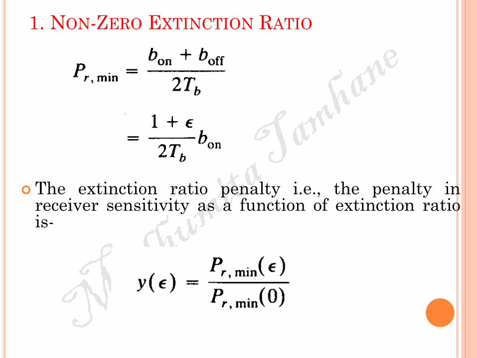
1. NON-ZERO EXTINCTION RATIO
The extinction ratio penalty i.e., the penalty in receiver sensitivity as a function of extinction ratio is-

2. FINITE PULSE WIDTH AND TIMING JITTER
Received optical pulse has a finite pulse width.
Some timing jitter is present.
Hence noise penalty is required for—
Non-optical filtering is needed to provide equalization
against pulse distortion or to minimize ISI.
Some ISI remains and degrades SNR.
To calculate magnitude of these effects, it is
necessary to define
Shape of received pulse.
The distribution of the jitter
We deal with only the former.
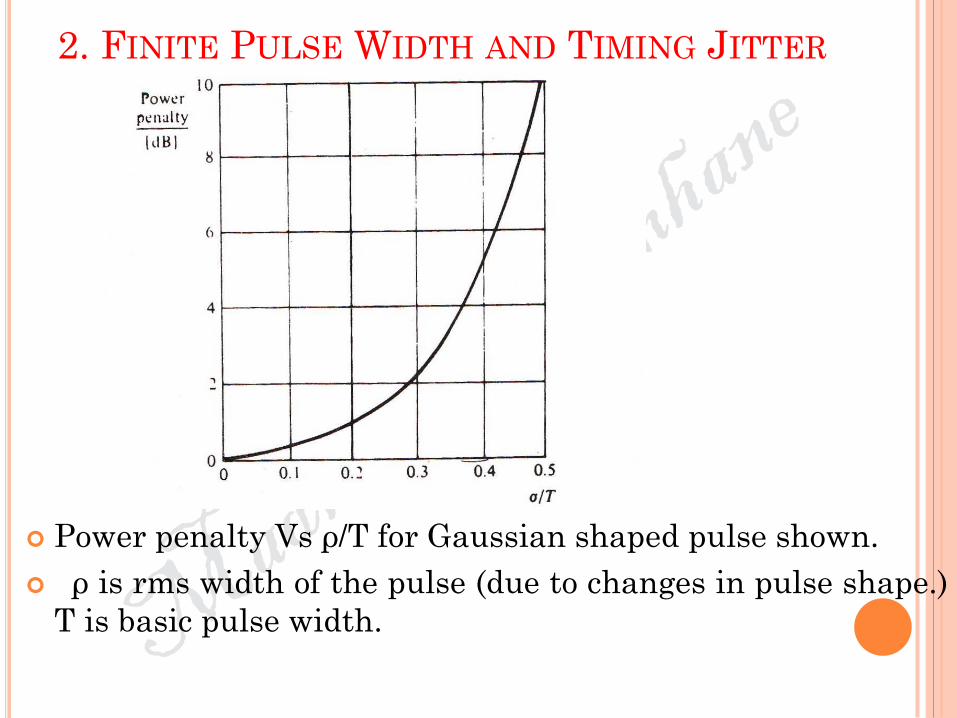
2. FINITE PULSE WIDTH AND TIMING JITTER
Power penalty Vs ρ/T for Gaussian shaped pulse shown.
ρ is rms width of the pulse (due to changes in pulse shape.)
T is basic pulse width.
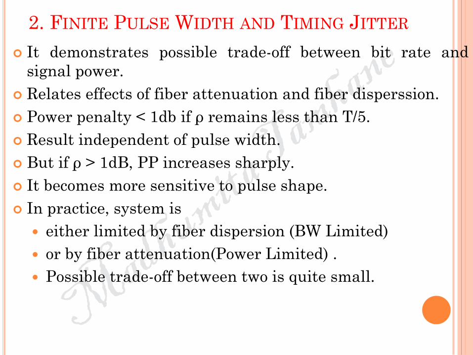
2. FINITE PULSE WIDTH AND TIMING JITTER
It demonstrates possible trade-off between bit rate and
signal power.
Relates effects of fiber attenuation and fiber disperssion.
Power penalty < 1db if ρ remains less than T/5.
Result independent of pulse width.
But if ρ > 1dB, PP increases sharply.
It becomes more sensitive to pulse shape.
In practice, system is
either limited by fiber dispersion (BW Limited)
or by fiber attenuation(Power Limited) .
Possible trade-off between two is quite small.

PREAMPLIFIER TYPES
Sensitivity and bandwidth of a receiver are effected by noise
sources at the front end, i.e. at preamplifier.
Preamplifier should give maximum receiver sensitivity with
desired bandwidth.
Three main types. But intermediate types can also be used.
PREAMPLIFIER TYPES – LOW IMPEDANCE (LZ)
Simplest, but not optimum design.
Photodiode operates into a low impedance amplifier
(appox.50Ω)
Bias or load resister Rb used to match amplifier impedance
by suppressing standing waves and give uniform frequency
response.
Rb with amplifier capacitance gives BW equal to or greater
than signal BW.
LZ amplifier can operate over a wide BW.
Gives low resistivity as a small voltage develops across
amplifier input and Rb .
Hence used only for short distance applications where
sensitivity not of concern.
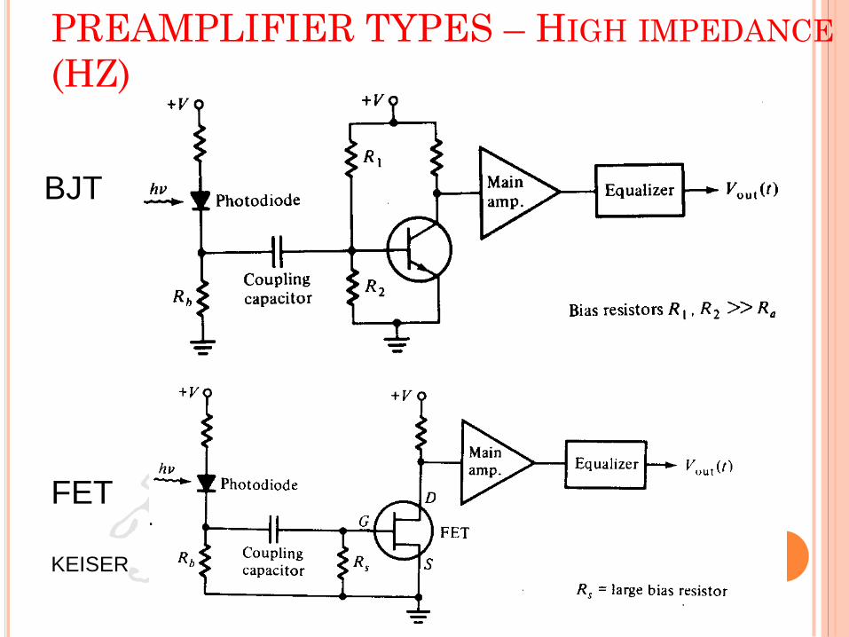
PREAMPLIFIER TYPES – HIGH IMPEDANCE
(HZ)
BJT
FET
KEISER
PREAMPLIFIER TYPES – HIGH IMPEDANCE
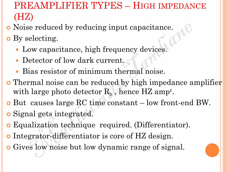
(HZ) Noise reduced by reducing input capacitance.
By selecting.
Low capacitance, high frequency devices.
Detector of low dark current.
Bias resistor of minimum thermal noise.
Thermal noise can be reduced by high impedance amplifier
with large photo detector Rb , hence HZ ampr.
But causes large RC time constant – low front-end BW.
Signal gets integrated.
Equalization technique required. (Differentiator).
Integrator-differentiator is core of HZ design.
Gives low noise but low dynamic range of signal.
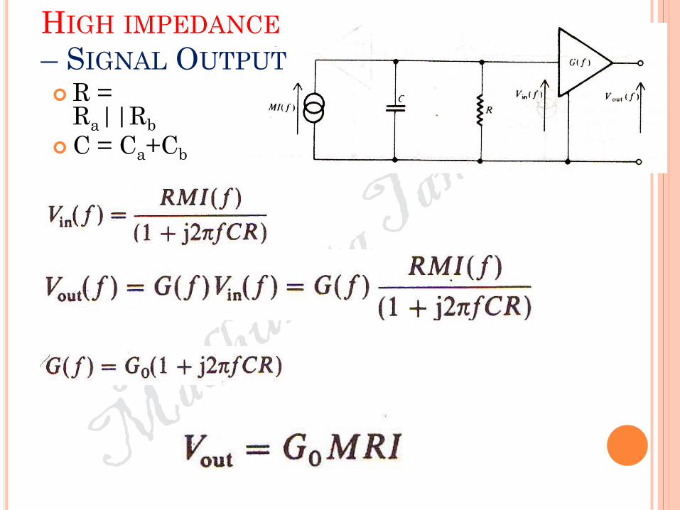
R = Ra||Rb
C = Ca+Cb
HIGH IMPEDANCE
– SIGNAL OUTPUT
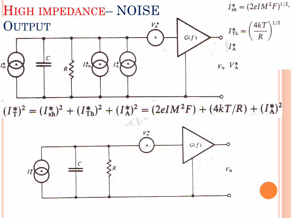
HIGH IMPEDANCE– NOISE
OUTPUT

HIGH IMPEDANCE– NOISE OUTPUT

HIGH IMPEDANCE (HZ)- ANALYSIS
SNR – K can be improved by increasing M until shot
noise term (iii) increases by F(M).
F(M) increases with M, gets comparable to other terms.
Has optimum value for M.
K improves by increasing front end R till (i) and (iv) are
significant. But increases RC. Hence requires more
equalization and low C.
If equalization required, (ii) dominates at high freq.
Noise increases as C2. Hence low C required.
Shot noise (iii) depends on input signal level.
Assumption of all noises statistical not true in reality.
All noises including F(M) not purely Gaussian.
HIGH IMPEDANCE (HZ)- ANALYSIS
Hence Actual SNR may be lesser.
Two limitations due to Integrator-differentiator
Equalization required for broadband applications.
limited dynamic range.
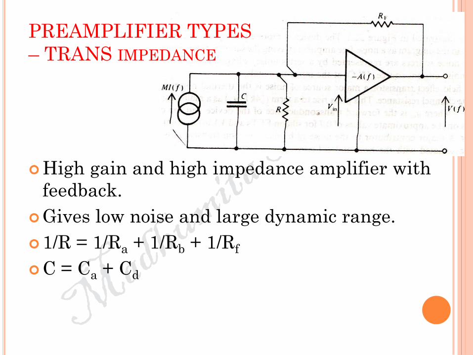
PREAMPLIFIER TYPES
– TRANS IMPEDANCE
High gain and high impedance amplifier with
feedback.
Gives low noise and large dynamic range.
1/R = 1/Ra + 1/Rb + 1/Rf
C = Ca + Cd
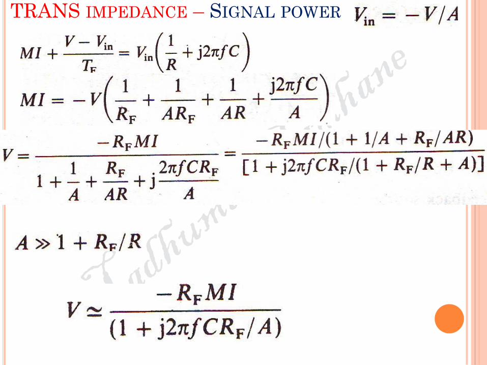
TRANS IMPEDANCE – SIGNAL POWER
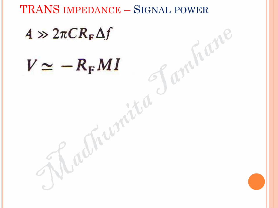
TRANS IMPEDANCE – SIGNAL POWER

TRANS IMPEDANCE – NOISE POWER

TRANS IMPEDANCE – NOISE POWER
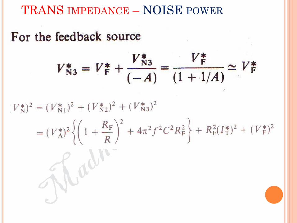
TRANS IMPEDANCE – NOISE POWER

TRANS IMPEDANCE – NOISE POWER
K = V/VN
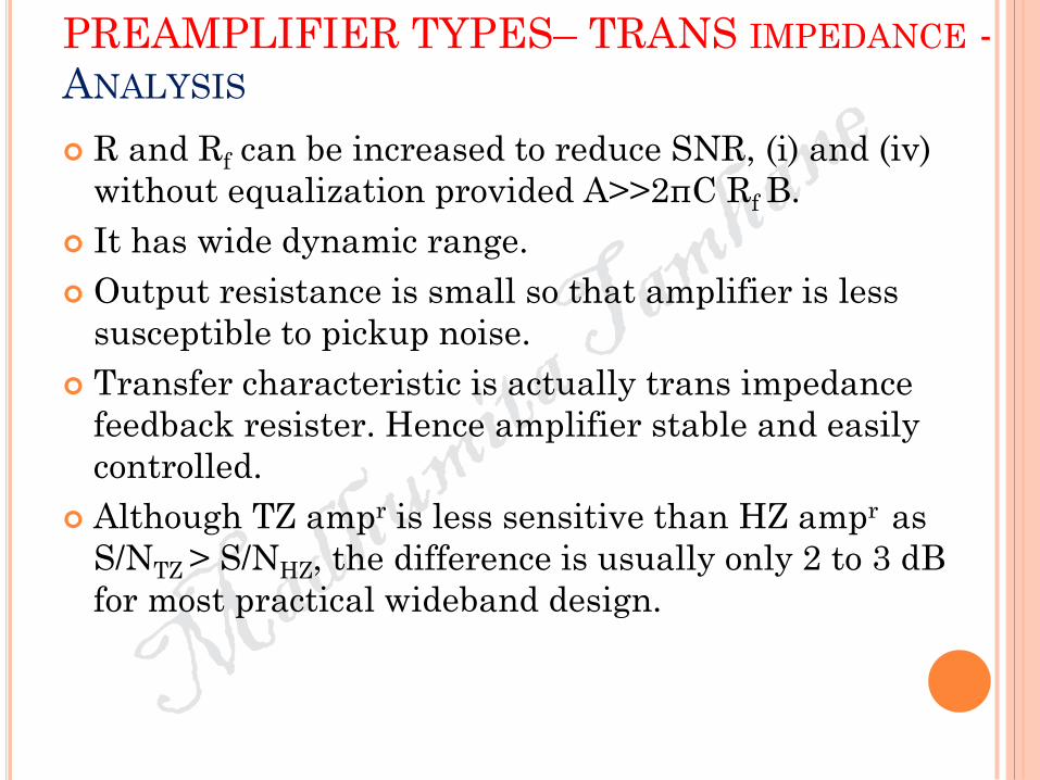
PREAMPLIFIER TYPES– TRANS IMPEDANCE -
ANALYSIS
R and Rf can be increased to reduce SNR, (i) and (iv)
without equalization provided A>>2πC Rf B.
It has wide dynamic range.
Output resistance is small so that amplifier is less
susceptible to pickup noise.
Transfer characteristic is actually trans impedance
feedback resister. Hence amplifier stable and easily
controlled.
Although TZ ampr is less sensitive than HZ ampr as
S/NTZ > S/NHZ, the difference is usually only 2 to 3 dB
for most practical wideband design.