Optical, Electronic and Structural Properties of Semiconductor Nanostructures and Optoelectronic...
47
Optical, Electronic and Structural Properties of Semiconductor Nanostructures and Optoelectronic Devices Inorganic Semi- conductors & Devices (Compounds of III- V, I-III-VI 2 , II- IV-V2) Organic Semi- conductors & Devices (Polymers & Functional Polymers) Solar Components & Systems (Photovoltaic und Solar Thermal) Prof. Dr. Gerhard Gobsch Department of Experimental Physics I
-
date post
20-Dec-2015 -
Category
Documents
-
view
234 -
download
2
Transcript of Optical, Electronic and Structural Properties of Semiconductor Nanostructures and Optoelectronic...
Optical, Electronic and Structural Properties of Semiconductor Nanostructures and Optoelectronic Devices
Inorganic Semi-conductors & Devices
(Compounds of III-V, I-III-VI2, II-IV-V2)
Organic Semi-conductors & Devices
(Polymers & Functional Polymers)
Solar Components & Systems
(Photovoltaic
und Solar Thermal)
Prof. Dr. Gerhard Gobsch
Department of Experimental Physics I
Organic Optoelectronics
ACOPhys, St. Petersburg, Sept 2006
An Introduction
Materials, Processing, Concepts and Devices
• Introduction• Molecular Energy Levels and
Charges• Materials and Processing• Devices• Summary
Organic Optoelectronics - Outline
Organic Optoelectronics
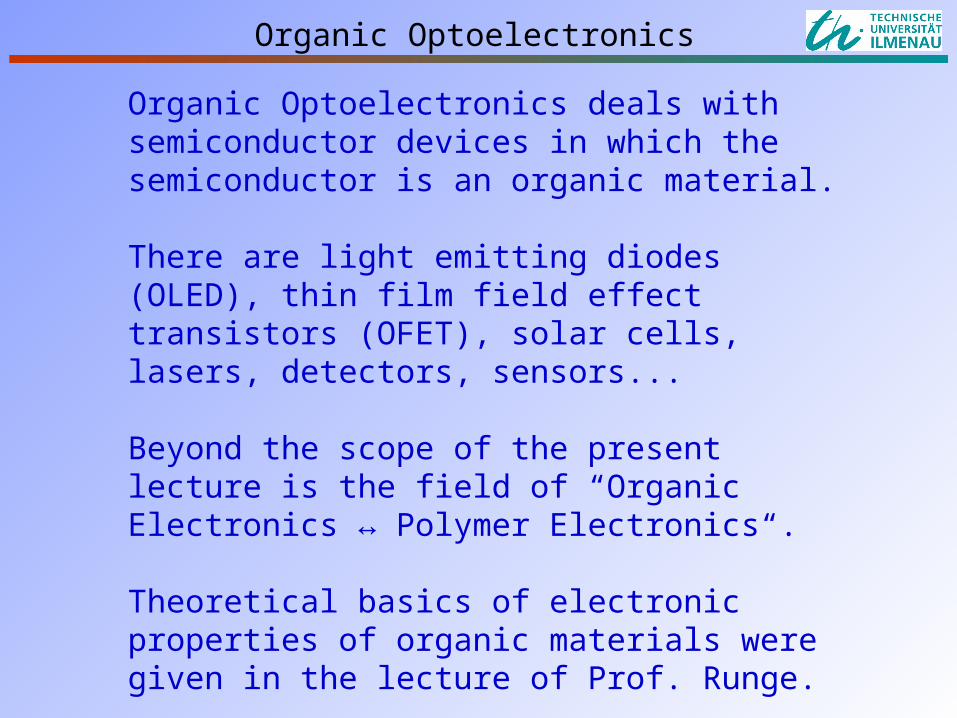
Organic Optoelectronics deals with semiconductor devices in which the semiconductor is an organic material.
There are light emitting diodes (OLED), thin film field effect transistors (OFET), solar cells, lasers, detectors, sensors...
Beyond the scope of the present lecture is the field of “Organic Electronics ↔ Polymer Electronics“.
Theoretical basics of electronic properties of organic materials were given in the lecture of Prof. Runge.
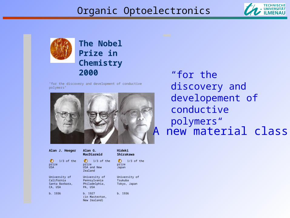
The Nobel Prize in Chemistry 2000
"for the discovery and development of conductive polymers"
Alan J. Heeger Alan G.
MacDiarmid Hideki Shirakawa
1/3 of the prize 1/3 of the prize 1/3 of the prize
USA USA and New Zealand
Japan
University of California Santa Barbara, CA, USA
University of Pennsylvania Philadelphia, PA, USA
University of Tsukuba Tokyo, Japan
b. 1936 b. 1927(in Masterton, New Zealand)
b. 1936
“for the discovery and developement of conductive polymers“
Organic Optoelectronics
A new material class!
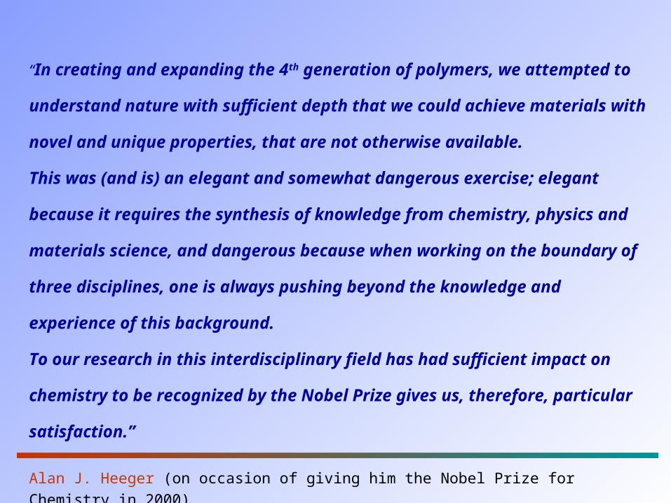
“In creating and expanding the 4th generation of polymers, we
attempted to understand nature with sufficient depth that we
could achieve materials with novel and unique properties, that
are not otherwise available.
This was (and is) an elegant and somewhat dangerous exercise;
elegant because it requires the synthesis of knowledge from
chemistry, physics and materials science, and dangerous
because when working on the boundary of three disciplines, one
is always pushing beyond the knowledge and experience of this
background.
To our research in this interdisciplinary field has had sufficient
impact on chemistry to be recognized by the Nobel Prize gives
us, therefore, particular satisfaction.”
Alan J. Heeger (on occasion of giving him the Nobel Prize for Chemistry in 2000)
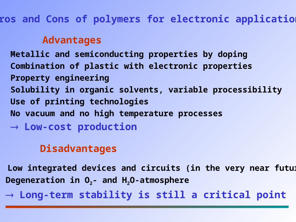
Advantages
Pros and Cons of polymers for electronic applications
• Metallic and semiconducting properties by doping• Combination of plastic with electronic properties• Property engineering• Solubility in organic solvents, variable processibility• Use of printing technologies• No vacuum and no high temperature processes
Low-cost production
Disadvantages
• Low integrated devices and circuits (in the very near future)
• Degeneration in O2- and H2O-atmosphere
Long-term stability is still a critical point
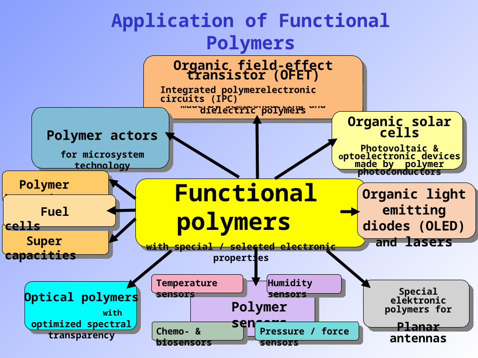
Application of Functional Polymers
Functional polymers with special / selected electronic properties
Organic field-effect transistor (OFET)
Polymerelektronikmade by semiconducting and dielectric polymers
Organic solar cellsPhotovoltaic & optoelectronic
devices made by polymer photoconductors
Polymer actorsfor microsystem technology
Optical polymers with optimized spectral
transparency
Special elektronic polymers for
Planar antennas
Organic light emitting diodes
(OLED) and lasers Super capacities
Polymer batteries
Polymer sensors
Fuel cells
Integrated polymerelectronic circuits (IPC)
Temperature sensors Humidity sensors
Chemo- & biosensors Pressure / force sensors
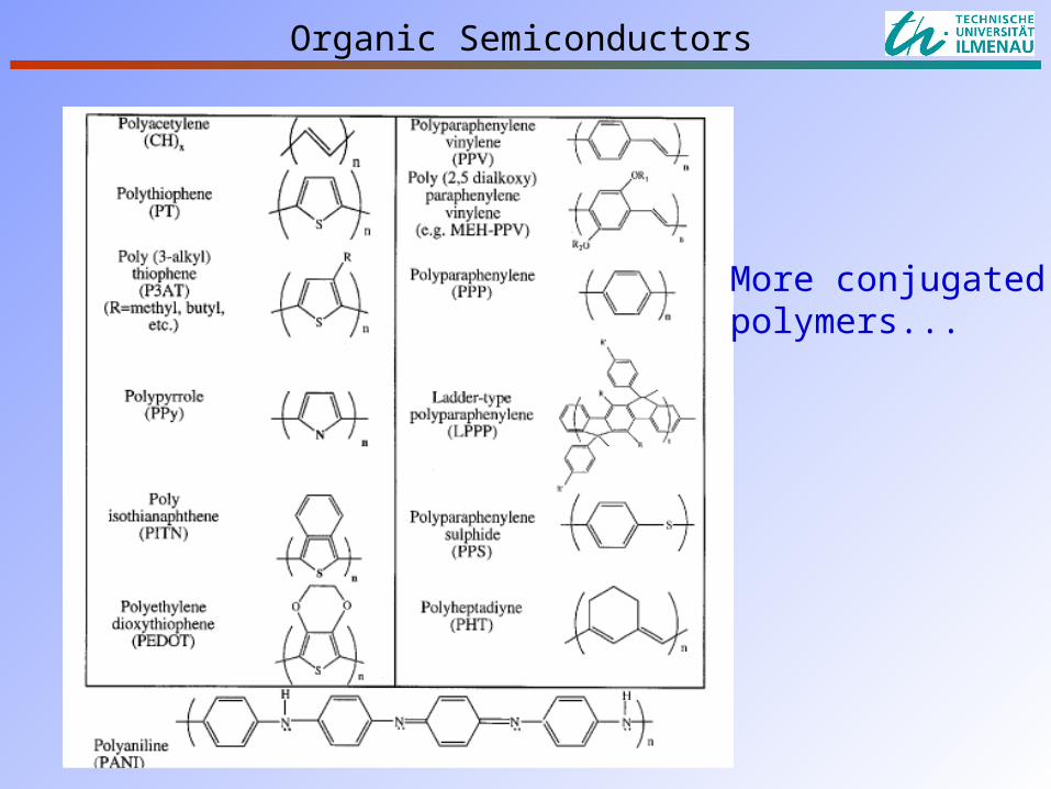
More conjugatedpolymers...
Organic Semiconductors
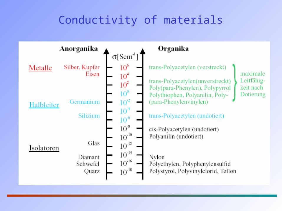
Conductivity of materials
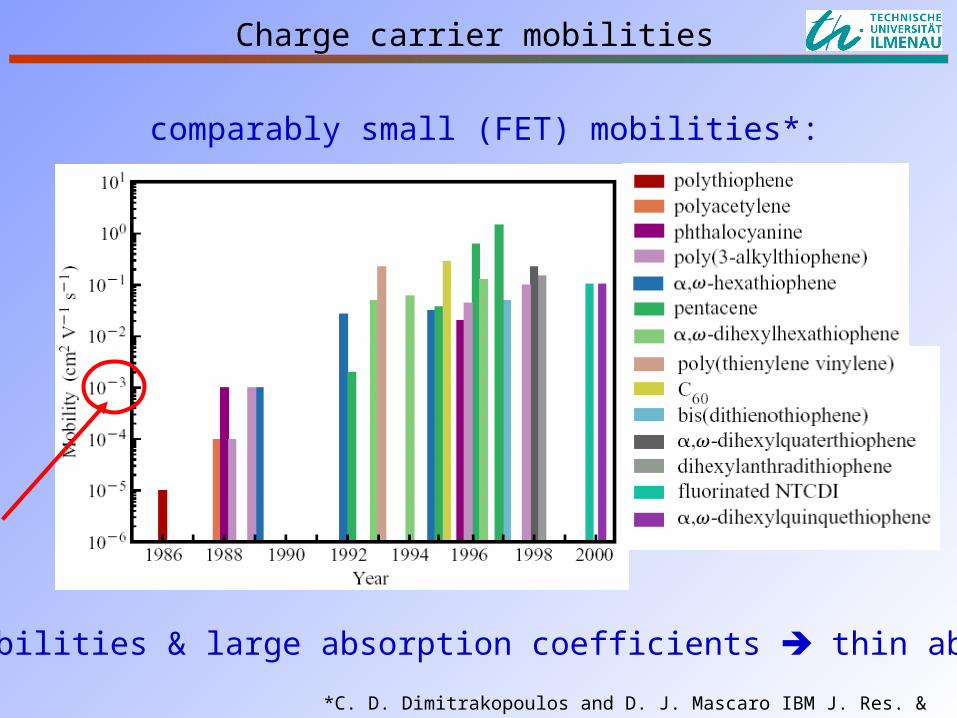
Charge carrier mobilities
comparably small (FET) mobilities*:
*C. D. Dimitrakopoulos and D. J. Mascaro IBM J. Res. & Dev. 45 (1), 2001
low mobilities & large absorption coefficients thin absorber
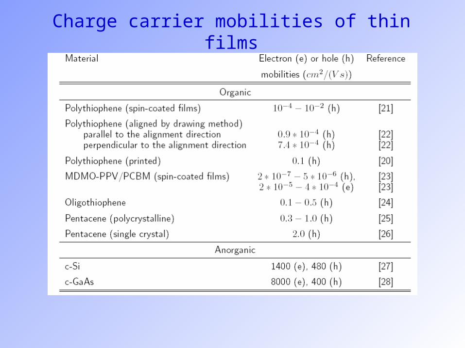
Charge carrier mobilities of thin films
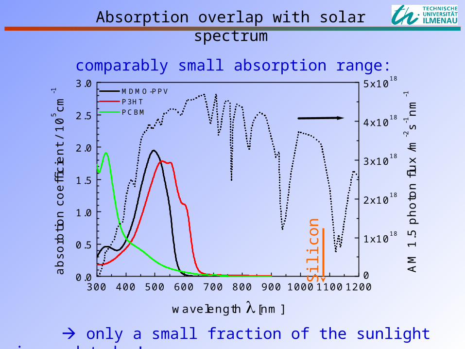
Absorption overlap with solar spectrum
comparably small absorption range:
only a small fraction of the sunlight is used today!
300 400 500 600 700 800 900 1000 1100 12000.0
0.5
1.0
1.5
2.0
2.5
3.0
0
1x10¹⁸
2x10¹⁸
3x10¹⁸
4x10¹⁸
5x10¹⁸
MDMO-PPV P3HT PCBM
abso
rbtio
n co
effic
ient
/ 10
5 cm-1
wavelength [nm]
AM
1.5
pho
ton
flux
/m-2s-1
nm-1
Sili
con
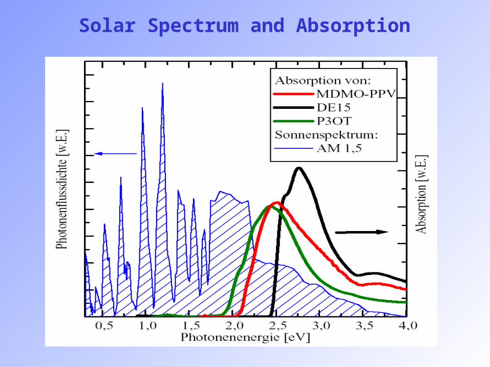
Solar Spectrum and Absorption
• Introduction• Molecular Energy Levels and
Charges• Materials and Processing• Devices• Summary
Organic Optoelectronics
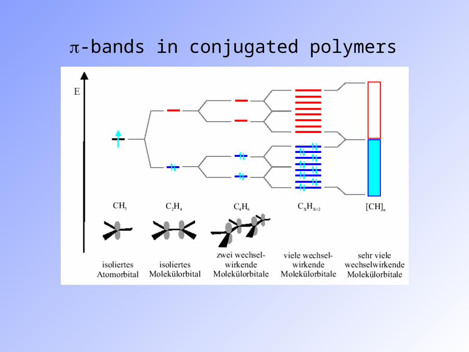
-bands in conjugated polymers
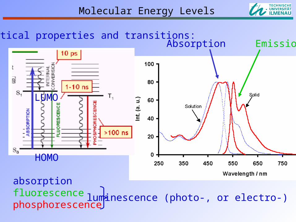
Molecular Energy Levels
HOMO
LUMO
Optical properties and transitions:Absorption Emission
absorptionfluorescencephosphorescence
luminescence (photo-, or electro-)
Molecular Energy Levels
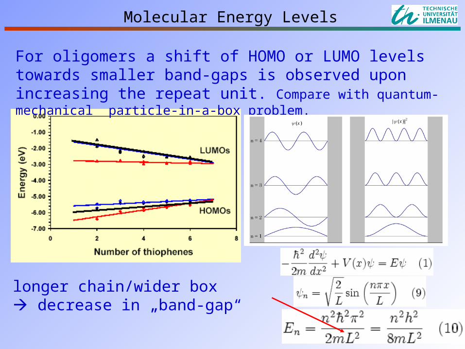
For oligomers a shift of HOMO or LUMO levels towards smaller band-gaps is observed upon increasing the repeat unit. Compare with quantum-mechanical particle-in-a-box problem.
longer chain/wider box decrease in „band-gap“
CC
CC
CC
CC
H H H H
H H H
CC
CC
CC
CC
H H H H
H H H
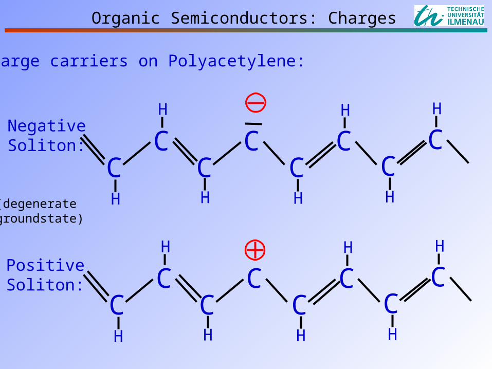
Organic Semiconductors: Charges
PositiveSoliton:
NegativeSoliton:
Charge carriers on Polyacetylene:
(degenerategroundstate)
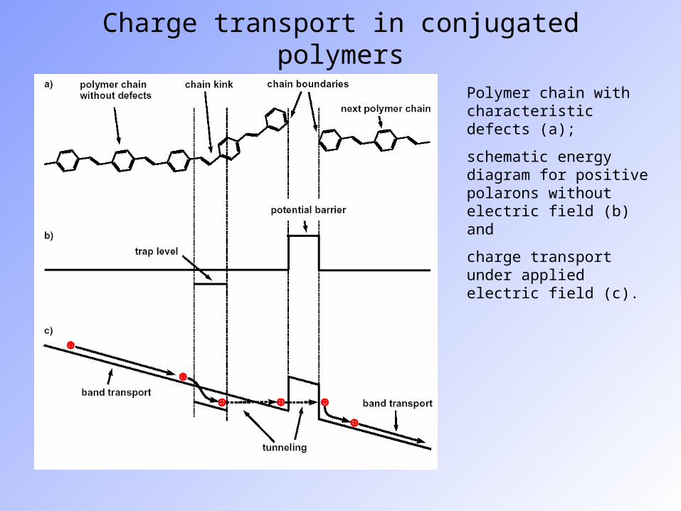
Charge transport in conjugated polymers
Polymer chain with characteristic defects (a);
schematic energy diagram for positive polarons without electric field (b) and
charge transport under applied electric field (c).
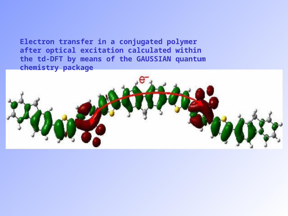
Electron transfer in a conjugated polymer after optical excitation calculated within the td-DFT by means of the GAUSSIAN quantum chemistry package

Charge carrier mobilities
comparably small (FET) mobilities*:
*C. D. Dimitrakopoulos and D. J. Mascaro IBM J. Res. & Dev. 45 (1), 2001
low mobilities & large absorption coefficients thin absorber
• Introduction• Molecular Energy Levels and
Charges• Materials and Processing• Devices• Summary
Organic Optoelectronics
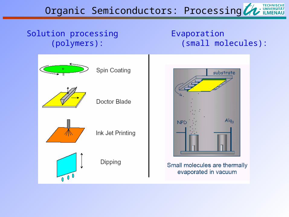
Organic Semiconductors: Processing
Solution processing Evaporation (polymers): (small molecules):
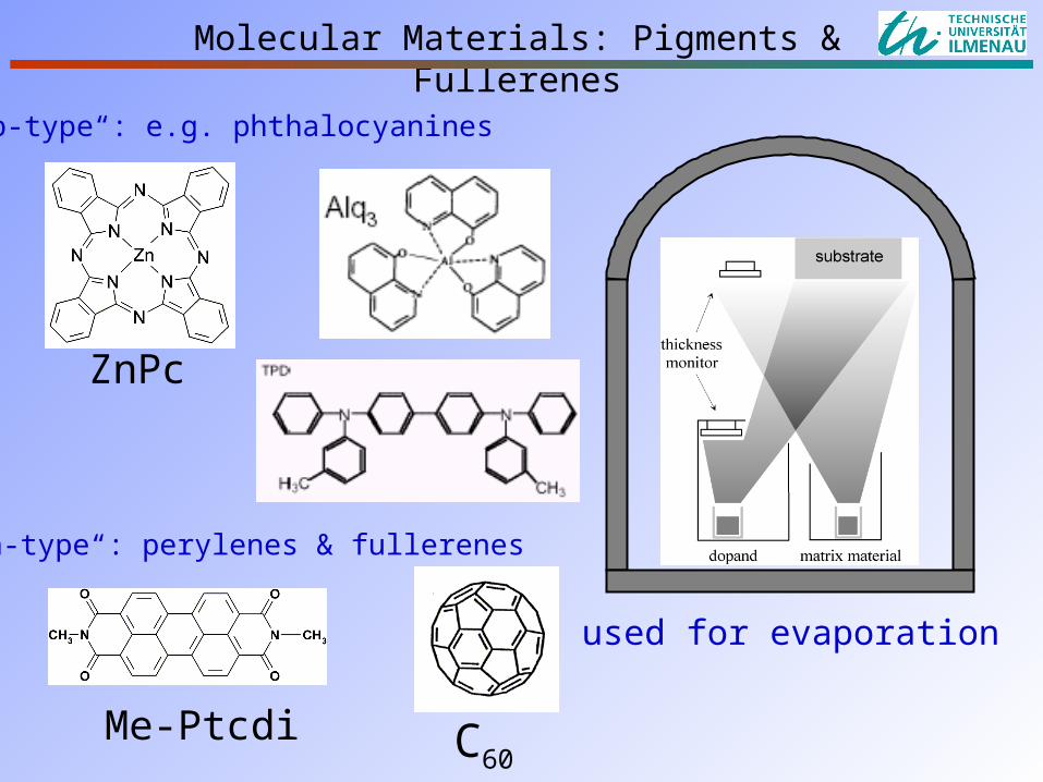
Molecular Materials: Pigments & Fullerenes
ZnPc
C6
0
Me-Ptcdi
„p-type“: e.g. phthalocyanines
„n-type“: perylenes & fullerenes
used for evaporation
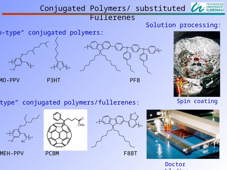
Conjugated Polymers/ substituted Fullerenes
Doctor blading
*
*
O
O
n
*
*
O
O
NCn
S ** n
CN-MEH-PPV PCBM F8BT
MDMO-PPV P3HT PFB
„p-type“ conjugated polymers:
„n-type“ conjugated polymers/fullerenes:
Solution processing:
Spin coating
NN
**
n
*
NN
S
*n
• Introduction• Molecular Energy Levels and
Charges• Materials and Processing• Devices• Summary
Organic Optoelectronics
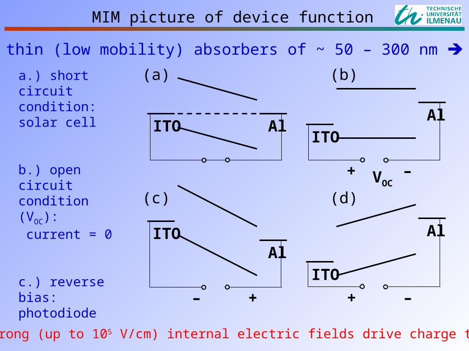
MIM picture of device function
ITO
ITO
ITO
ITO
Al
Al
Al
Al
+ – – +
+ – VOC
(a) (b)
(c) (d)
a.) short circuit condition: solar cell
b.) open circuit condition (VOC): current = 0
c.) reverse bias: photodiode
d.) forward bias: light emitting diodeStrong (up to 105 V/cm) internal electric fields drive charge transport
Very thin (low mobility) absorbers of ~ 50 – 300 nm MIM
Organic Semiconductor Devices
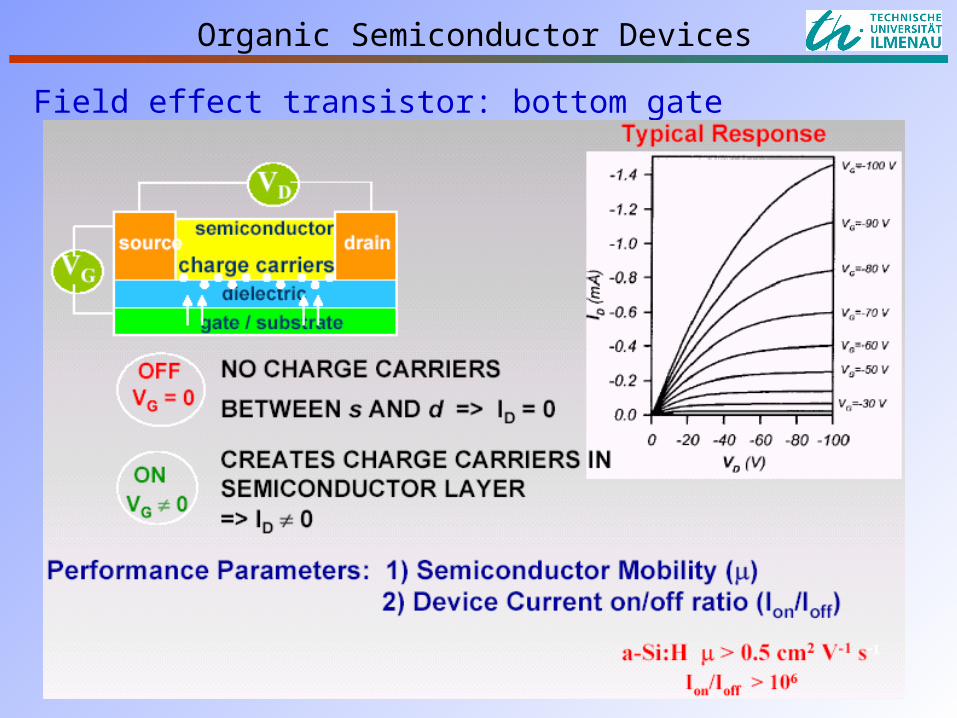
Field effect transistor: bottom gate (usually Si/SiO2)
W. Fix, A. Ullmann, J. Ficker, and W. Clemens, Applied Physics Letters 81, 9, p. 1735 (2002)
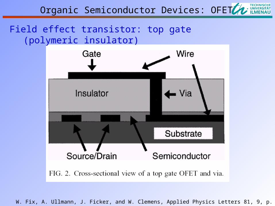
Field effect transistor: top gate (polymeric insulator)
Organic Semiconductor Devices: OFET
*C. D. Dimitrakopoulos and D. J. Mascaro IBM J. Res. & Dev. 45 (1), 2001
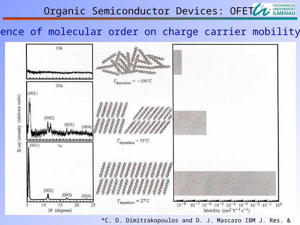
Organic Semiconductor Devices: OFET
Influence of molecular order on charge carrier mobility:
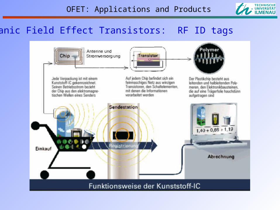
Organic Field Effect Transistors: RF ID tags
OFET: Applications and Products
Organic light emitting diode (OLED):
Organic Semiconductor Devices: OLED
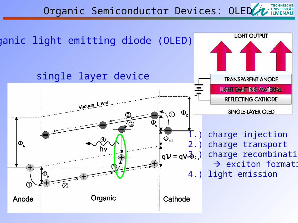
1.) charge injection2.) charge transport3.) charge recombination exciton formation4.) light emission
single layer device
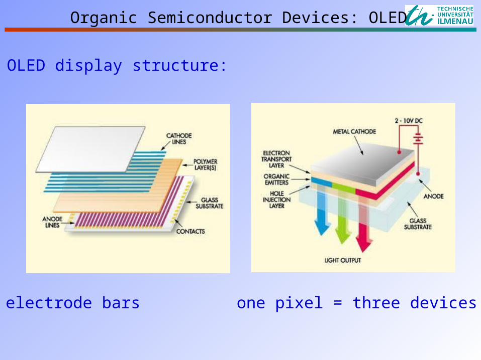
OLED display structure:
electrode bars one pixel = three devices
Organic Semiconductor Devices: OLED
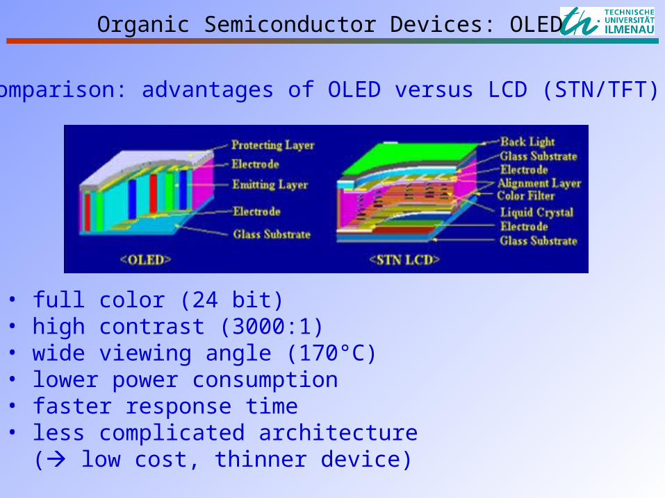
Comparison: advantages of OLED versus LCD (STN/TFT)
• full color (24 bit)• high contrast (3000:1)• wide viewing angle (170°C)• lower power consumption• faster response time• less complicated architecture ( low cost, thinner device)
Organic Semiconductor Devices: OLED
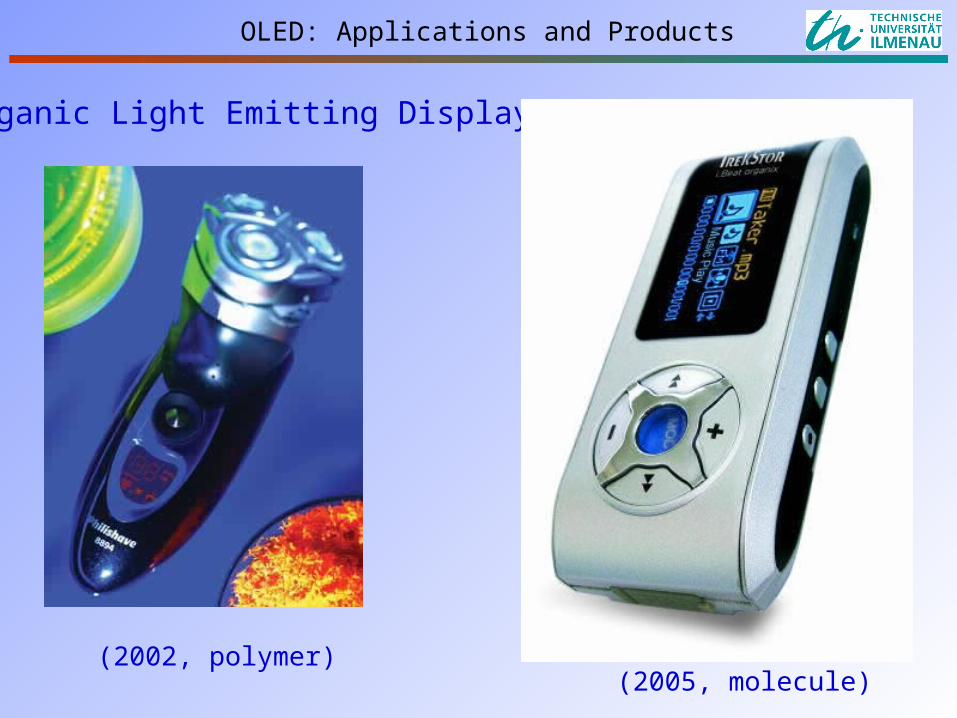
OLED: Applications and Products
Organic Light Emitting Displays:
(2005, molecule)(2002, polymer)
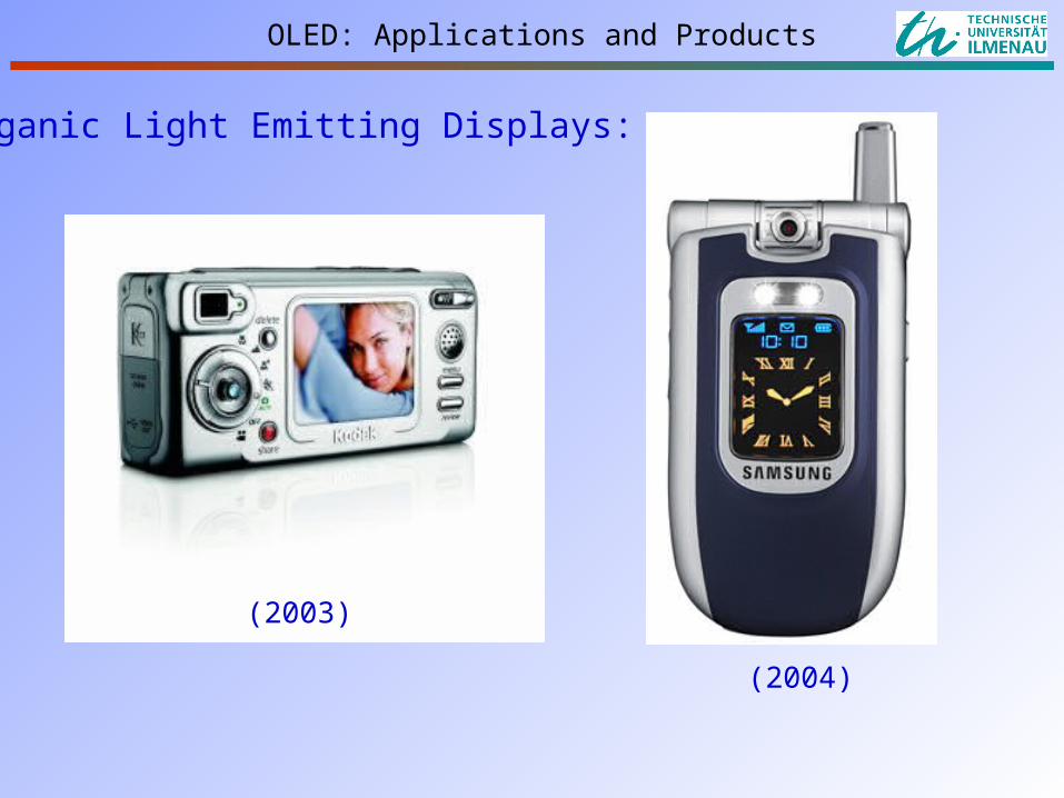
(2003)
(2004)
Organic Light Emitting Displays:
OLED: Applications and Products
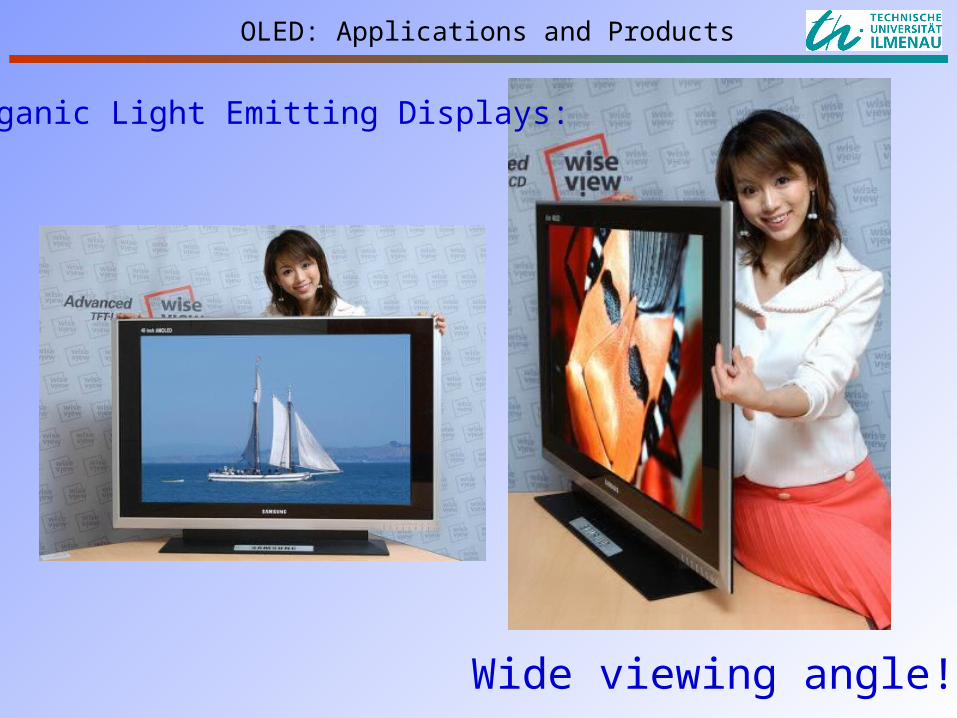
Wide viewing angle!
Organic Light Emitting Displays:
OLED: Applications and Products
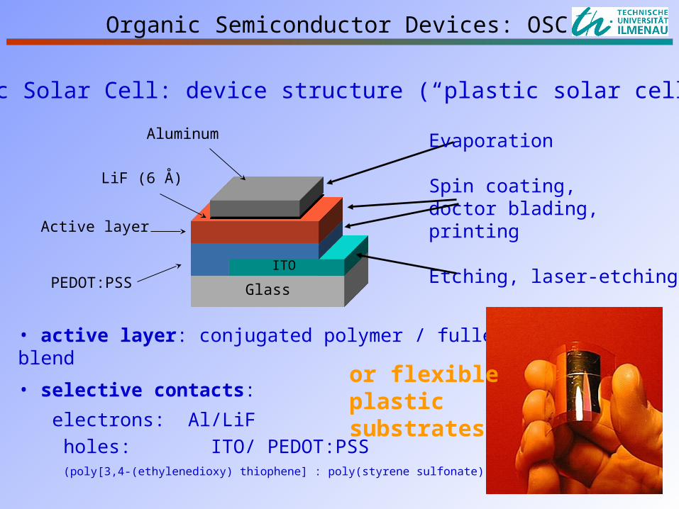
• active layer: conjugated polymer / fullerene blend
• selective contacts:
electrons: Al/LiF
holes: ITO/ PEDOT:PSS
(poly[3,4-(ethylenedioxy) thiophene] : poly(styrene sulfonate))
PEDOT:PSS
Active layer
LiF (6 Å)
Aluminum
ITO
Glass
Evaporation
Spin coating,doctor blading,printing
Etching, laser-etching
Organic Solar Cell: device structure (“plastic solar cell“):
Organic Semiconductor Devices: OSC
or flexibleplasticsubstrates
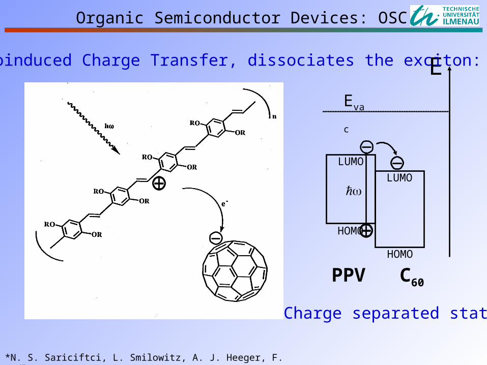
*N. S. Sariciftci, L. Smilowitz, A. J. Heeger, F. Wudl, Science 258, 1474 (1992)
PPV C60
EEva
c
HOMO
HOMO
LUMO
LUMO
Charge separated state!
Organic Semiconductor Devices: OSC
Photoinduced Charge Transfer, dissociates the exciton:
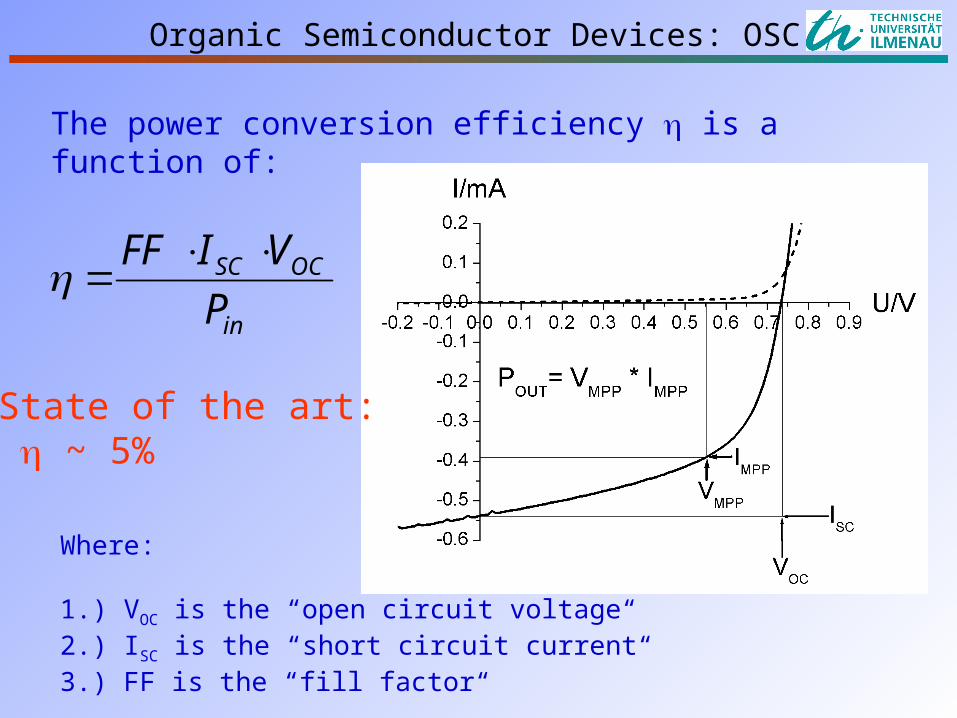
The power conversion efficiency is a function of:
in
OCSC
P
VIFF
Where:
1.) VOC is the “open circuit voltage“2.) ISC is the “short circuit current“3.) FF is the “fill factor“
Organic Semiconductor Devices: OSC
State of the art: ~ 5%
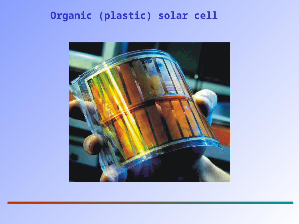
Organic (plastic) solar cell
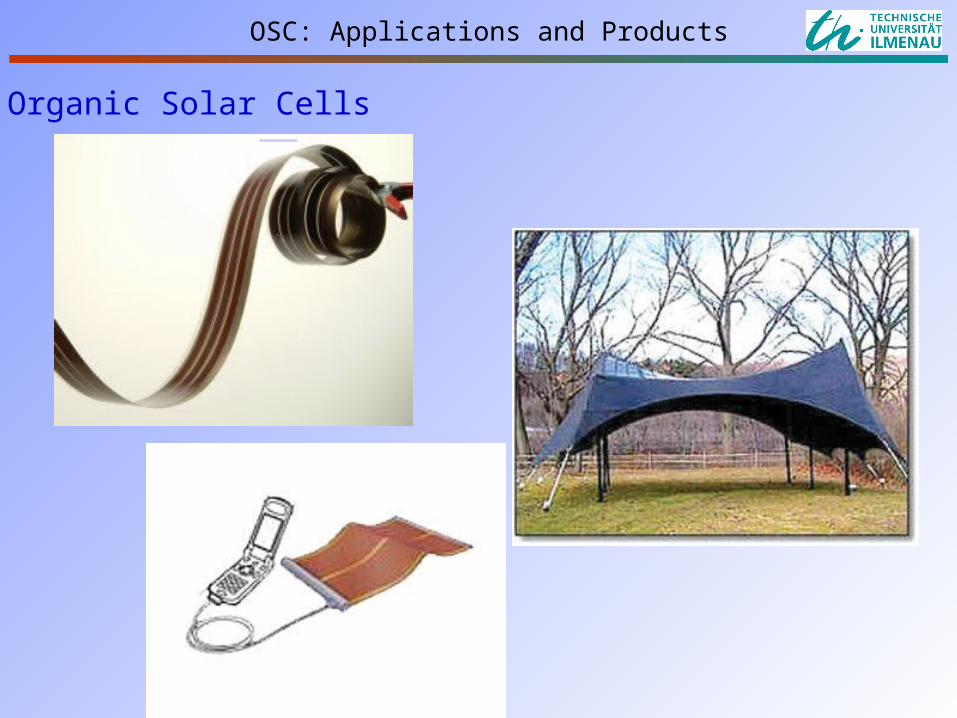
Organic Solar Cells
OSC: Applications and Products
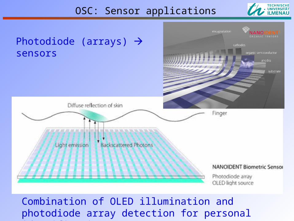
OSC: Sensor applications
Photodiode (arrays) sensors
Combination of OLED illumination and photodiode array detection for personal identification.
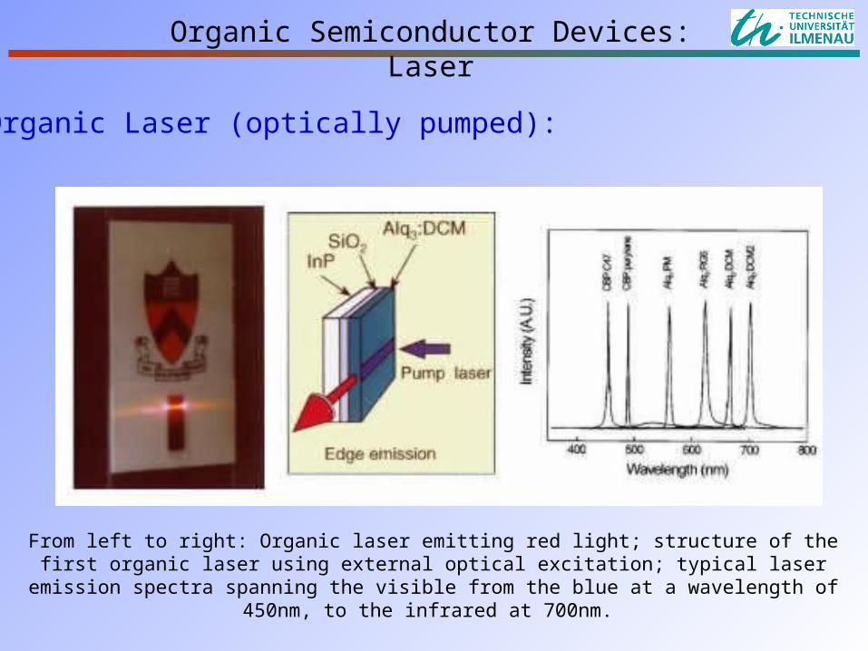
Organic Laser (optically pumped):
From left to right: Organic laser emitting red light; structure of the first organic laser using external optical excitation; typical laser emission spectra spanning the visible
from the blue at a wavelength of 450nm, to the infrared at 700nm.
Organic Semiconductor Devices: Laser
• Introduction• Molecular Energy Levels and
Charges• Materials and Processing• Devices• Summary
Organic Optoelectronics
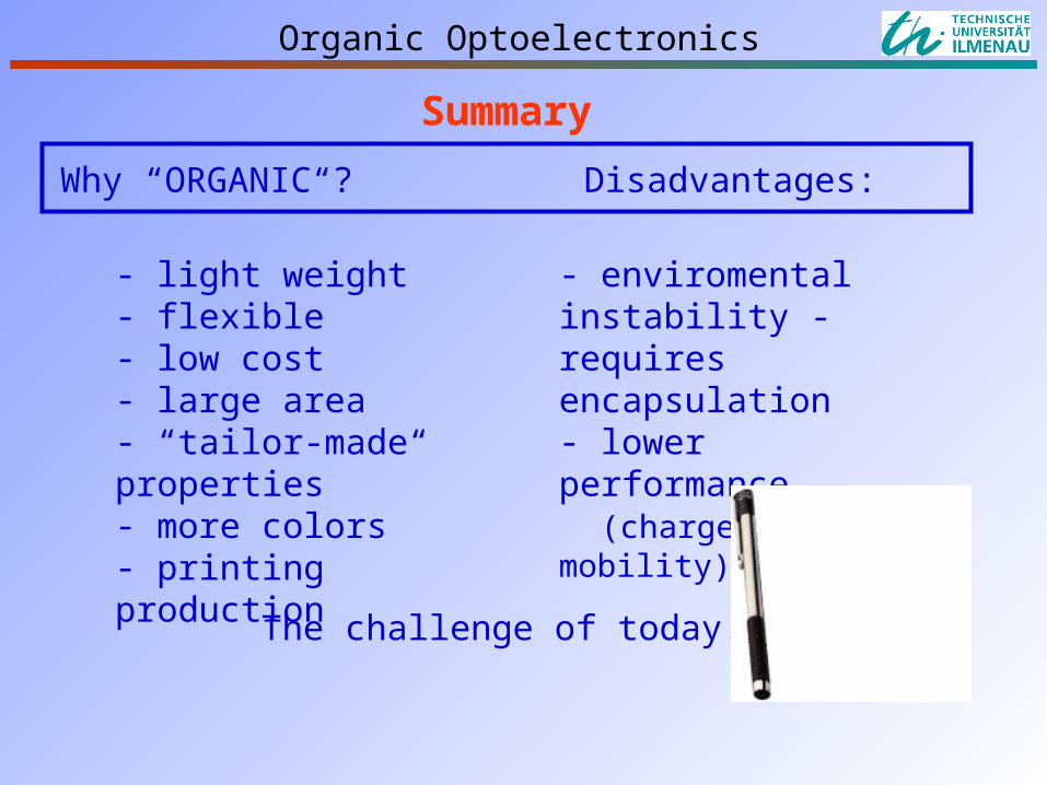
Why “ORGANIC“? Disadvantages:
Organic Optoelectronics
- light weight- flexible- low cost- large area- “tailor-made“ properties- more colors- printing production
- enviromental instability - requires encapsulation- lower performance (charge carrier mobility)
The challenge of today!
Summary