Optical Basics MEMS - RIT - People · Optical Basics - MEMS Page 1 ... 436 nm 0.5 0.0 Wavelength...
49
© December 20, 2016 Dr. Lynn Fuller, Professor Optical Basics - MEMS Page 1 Rochester Institute of Technology Microelectronic Engineering ROCHESTER INSTITUTE OF TECHNOLOGY MICROELECTRONIC ENGINEERING Optical Basics _MEMS Dr. Lynn Fuller Webpage: http://people.rit.edu/lffeee Microelectronic Engineering Rochester Institute of Technology 82 Lomb Memorial Drive Rochester, NY 14623-5604 Email: [email protected] Program Webpage: http:// www.rit.edu/microelectronic/ 12-20-2016 Optical_Basics_MEMS.ppt
Transcript of Optical Basics MEMS - RIT - People · Optical Basics - MEMS Page 1 ... 436 nm 0.5 0.0 Wavelength...

© December 20, 2016 Dr. Lynn Fuller, Professor
Optical Basics - MEMS
Page 1
Rochester Institute of Technology
Microelectronic Engineering
ROCHESTER INSTITUTE OF TECHNOLOGYMICROELECTRONIC ENGINEERING
Optical Basics _MEMS
Dr. Lynn FullerWebpage: http://people.rit.edu/lffeee
Microelectronic EngineeringRochester Institute of Technology
82 Lomb Memorial DriveRochester, NY 14623-5604
Email: [email protected] Webpage: http://www.rit.edu/microelectronic/
12-20-2016 Optical_Basics_MEMS.ppt

© December 20, 2016 Dr. Lynn Fuller, Professor
Optical Basics - MEMS
Page 2
Rochester Institute of Technology
Microelectronic Engineering
OUTLINE
Light Sources
Light Detectors
Optic Components
Mirrors
Light Emissive Devices
Light Modulators
References
Homework

© December 20, 2016 Dr. Lynn Fuller, Professor
Optical Basics - MEMS
Page 3
Rochester Institute of Technology
Microelectronic Engineering
SPECTRICAL DISTRIBUTION OF SOLAR RADIANT POWER
From: Micromachined Transducers, Gregory T.A. Kovacs

© December 20, 2016 Dr. Lynn Fuller, Professor
Optical Basics - MEMS
Page 4
Rochester Institute of Technology
Microelectronic Engineering
BLACK BODY, AM0 AND AM1.5
From: Solar Cells, Martin A. Green, Prentice Hall

© December 20, 2016 Dr. Lynn Fuller, Professor
Optical Basics - MEMS
Page 5
Rochester Institute of Technology
Microelectronic Engineering
BLACK BODY RADIATION
From: Solar Cells, Martin A. Green, Prentice HallFrom: Micromachined Transducers, Gregory T.A. Kovacs
Wien’s Displacement Law
lpeak = 2898/T (µm)
lpeak = 2898 µm / T
h = 6.6262E-34 J s = 4.1361E-15 eV s
l= c/n k=1.38e-23 J/K
Wl = radiant flux
e(l) = emissivity (dimensionless, e=1 for black body)

© December 20, 2016 Dr. Lynn Fuller, Professor
Optical Basics - MEMS
Page 6
Rochester Institute of Technology
Microelectronic Engineering
PLANCK’S LAW
I is spectral radiance (w/m2/…….)
Wl is radiant flux (w/m2)
h = 6.6262E-34 J s = 4.1361E-15 eV s
l= wavelength = c/n
n = frequency
c = 2.998E8 m/s
k =1.38e-23 J/K
e(l) = emissivity (dimensionless, e=1 for black body)
Planck’s Law: (Spectral Radiance) Power per unit time radiated per unit area of emitting surface in the normal direction per unit solid angle per unit frequency.
This equation is used to approximate emissions from black body sources.

© December 20, 2016 Dr. Lynn Fuller, Professor
Optical Basics - MEMS
Page 7
Rochester Institute of Technology
Microelectronic Engineering
HOT FILIMENT “BLACK BODY” LIGHT SOURCES
600 µm
100 µm
Dave BorkholderSenior project 1993
MOVIE

© December 20, 2016 Dr. Lynn Fuller, Professor
Optical Basics - MEMS
Page 8
Rochester Institute of Technology
Microelectronic Engineering
EMISSION SPECTRA OF THE Hg VAPOR BULB
300 400 500 600 700
1.0i-line, 365 nm
g-line, 436 nm
0.5
0.0
Wavelength (nm)
h f
e

© December 20, 2016 Dr. Lynn Fuller, Professor
Optical Basics - MEMS
Page 9
Rochester Institute of Technology
Microelectronic Engineering
LED IV CHARACTERISTICS
VD
ID
2.0
LED
-10.0
Light
Flat
n
p
Light Emitting Diode -LED
- Va +

© December 20, 2016 Dr. Lynn Fuller, Professor
Optical Basics - MEMS
Page 10
Rochester Institute of Technology
Microelectronic Engineering
LIGHT EMITTING DIODES (LEDs)
P-side N-side
Space
charge
Layer
LightLight
Hole concentration vs distnace
xx
Electron concentration vs distance
In the forward biased diode current flows and as holes recombine on the n-side or electrons recombine on the p-side, energy is given off as light, with wavelength appropriate for the energy gap for that material. l = h c / E
h = Plank’s constantc = speed of light

© December 20, 2016 Dr. Lynn Fuller, Professor
Optical Basics - MEMS
Page 11
Rochester Institute of Technology
Microelectronic Engineering
LEDs
SFH4110
SEP8736
SEP8736

© December 20, 2016 Dr. Lynn Fuller, Professor
Optical Basics - MEMS
Page 12
Rochester Institute of Technology
Microelectronic Engineering
RIT’S FIRST LED
GaP wafers with n-type epilayer, add
gold metal, dice and wire bond to RIT
thick film ceramic package.

© December 20, 2016 Dr. Lynn Fuller, Professor
Optical Basics - MEMS
Page 13
Rochester Institute of Technology
Microelectronic Engineering
RELATIVE LUMINOSITY VS WAVELENGTH
Human eye perceives 550nm (green-yellow) as the brightest, the relative luminosity of other colors is give above

© December 20, 2016 Dr. Lynn Fuller, Professor
Optical Basics - MEMS
Page 14
Rochester Institute of Technology
Microelectronic Engineering
PHOTODIODE
B -
P+ Ionized Immobile Phosphrous donor atom
Ionized Immobile Boron acceptor atom
Phosphrous donor atom and electronP+
-
B-
+Boron acceptor atom and hole
n-type
p-type
B - P+
B -B -
B -B -
P+ P+P+P+
P+
P+
P+
-
B-
+
eB -B -
P+
-P+
-P+
-
B-
+
-+
-+
I
electron
and hole
pair
-+
-+
space charge layer

© December 20, 2016 Dr. Lynn Fuller, Professor
Optical Basics - MEMS
Page 15
Rochester Institute of Technology
Microelectronic Engineering
CHARGE GENERATION IN SEMICONDUCTORS
E = hn = hc / l
What wavelengths will not
generate e-h pairs in silicon.
Thus silicon is transparent or
light of this wavelength or
longer is not adsorbed?
From: Micromachined Transducers,
Gregory T.A. Kovacs
Material Bandgap
eV @ 300°K
lmax
(um)
GaN 3.360 0.369
ZnO 3.350 0.370
SiC 2.996 0.414
CdS 2.420 0.512
GaP 2.260 0.549
CdSe 1.700 0.729
GaAs 1.420 0.873
InP 1.350 0.919
Si 1.120 1.107
Ge 0.660 1.879
PbS 0.410 3.024
PbTe 0.310 4.000
InSb 0.170 7.294

© December 20, 2016 Dr. Lynn Fuller, Professor
Optical Basics - MEMS
Page 16
Rochester Institute of Technology
Microelectronic Engineering
WIDTH OF SPACE CHARGE LAYER
Width of space charge
layer depends on the
doping on both sides
and the applied reverse
bias voltage and
temperature.

© December 20, 2016 Dr. Lynn Fuller, Professor
Optical Basics - MEMS
Page 17
Rochester Institute of Technology
Microelectronic Engineering
CHARGE GENERATION vs WAVELENGTH
II
n-type
p-type
e
l1 l3 l4l2
E = hn = hc / l
h = 6.625 e-34 j/s
= (6.625 e-34/1.6e-19) eV/s
E = 1.55 eV (red)
E = 2.50 eV (green)
E = 4.14 eV (blue) B - P+
B -B -
B -B -
P+ P+P+P+
P+
P+
P+
-
B-
+
B -B -
P+
-P+
-P+
-
B-
+
-+-
+-
+
To generate e-h pair in silicon we need E > Egap
E > 1.12 eV

© December 20, 2016 Dr. Lynn Fuller, Professor
Optical Basics - MEMS
Page 18
Rochester Institute of Technology
Microelectronic Engineering
ADSORPTION VERSUS DISTANCE
I
V
n
p
IV
I
+
V
-
More Light
No Light
Most Light
f(x) = f(0) exp-a x
Find % adsorbed for Green light
at x=5 µm and Red light at 5 µm
1.00E-06
1.00E-05
1.00E-04
1.00E-03
1.00E-02
1.00E-01
1.00E+00
1.00E+01
1.00E+02
1.00E+03
1.00E+04
1.00E+05
1.00E+06
250 450 650 850 1050 1250 1450
Adsorption Coefficient vs Wavelength
Wavelength (nm)
Adso
rpti
on C
oef
fici
ent,
a (
1/c
m) For Silicon

© December 20, 2016 Dr. Lynn Fuller, Professor
Optical Basics - MEMS
Page 19
Rochester Institute of Technology
Microelectronic Engineering
PN JUNCTION DESIGN FOR PHOTO DIODE
0µm 1µm 2µm 3µm 4µm
67%
100%
@850nm
@550nm
1017
1015
Space Charge Layer
60%

© December 20, 2016 Dr. Lynn Fuller, Professor
Optical Basics - MEMS
Page 20
Rochester Institute of Technology
Microelectronic Engineering
PIN, AVALANCE PHOTODIODES (APD)
n-sidep-side
IntrinsicP I N
W2W1 0 0
PIN and Avalance photo diodes (APD) are made with an intrinsic (almost zero doping) layer between the N and P layers. The depletion layer is increased by the width of the Intrinsic layer. Avalance diodes are the same structure but used with large reverse bias (>100 volts) that creates large electric field in the space charge layer that can accelerate the electrons to velocities high enough to cause ionizing collisions giving a multiplication of carriers. Each photon can generate hundreds of electron hole pairs.

© December 20, 2016 Dr. Lynn Fuller, Professor
Optical Basics - MEMS
Page 21
Rochester Institute of Technology
Microelectronic Engineering
PIN, AVALANCE PHOTODIODES (APD)
www.silicon-sensor.com

© December 20, 2016 Dr. Lynn Fuller, Professor
Optical Basics - MEMS
Page 22
Rochester Institute of Technology
Microelectronic Engineering
Photo Multiplier Tube (low work Function)
-2000 V
-3000 V
-4000 V
hv-1000 V
R
Vout
PHOTOMULTIPLIER

© December 20, 2016 Dr. Lynn Fuller, Professor
Optical Basics - MEMS
Page 23
Rochester Institute of Technology
Microelectronic Engineering
CHARGE COLLECTION IN MOS STRUCTURES
e
-+
-+
electron
and hole
pair
-+
-+
depletion region
-+
-- -
p-type
+ V
B -
B -
B -
B -
l1 l3 l4l2
thin poly gate
E = hn = hc / l
h = 6.625 e-34 j/s
= (6.625 e-34/1.6e-19) eV/s
E = 1.55 eV (red)
E = 2.50 eV (green)
E = 4.14 eV (blue)
© December 20, 2016 Dr. Lynn Fuller, Professor
Optical Basics - MEMS
Page 24
Rochester Institute of Technology
Microelectronic Engineering
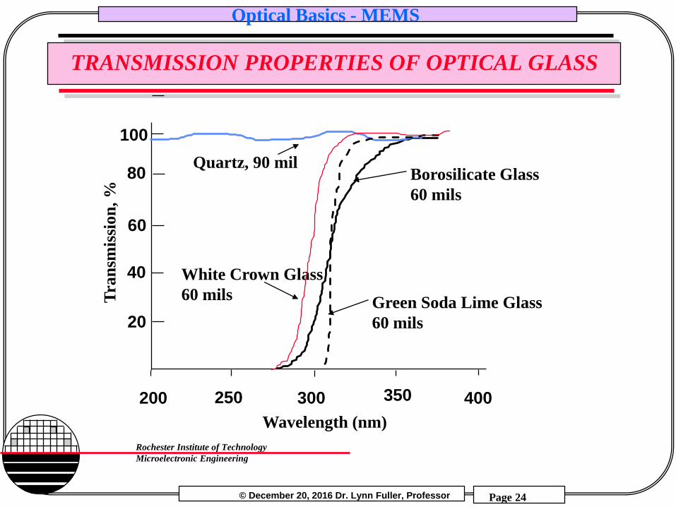
TRANSMISSION PROPERTIES OF OPTICAL GLASS
200 400300250 350
Wavelength (nm)
Green Soda Lime Glass
60 mils
White Crown Glass
60 mils
Borosilicate Glass
60 mils
Tra
nsm
issi
on
, %
20
40
60
100
80Quartz, 90 mil

© December 20, 2016 Dr. Lynn Fuller, Professor
Optical Basics - MEMS
Page 25
Rochester Institute of Technology
Microelectronic Engineering
THERMOPILE SENSOR
www.heimannsensor.com

© December 20, 2016 Dr. Lynn Fuller, Professor
Optical Basics - MEMS
Page 26
Rochester Institute of Technology
Microelectronic Engineering
RIT THERMOPILE SENSOR
Output voltage vs Input power for wafer 4
-50
0
50
100
150
200
250
300
350
0 0.1 0.2 0.3 0.4 0.5
Input power(mW)
Ou
tpu
t V
olt
ag
e(u
V)
Die 3 ,
R= 12.2
Kohms
Die 5,
R=
14.32
kohmsDie 6 ,
R=
14.32
kohmsDie 7,
R= 15
Kohms
Usha Kuppuswamy, 2005

© December 20, 2016 Dr. Lynn Fuller, Professor
Optical Basics - MEMS
Page 27
Rochester Institute of Technology
Microelectronic Engineering
FIBER OPTIC COMPONENTS

© December 20, 2016 Dr. Lynn Fuller, Professor
Optical Basics - MEMS
Page 28
Rochester Institute of Technology
Microelectronic Engineering
LASER AND FRESNEL LENS

© December 20, 2016 Dr. Lynn Fuller, Professor
Optical Basics - MEMS
Page 29
Rochester Institute of Technology
Microelectronic Engineering
OPTICAL SYSTEM
Fresnel Lens

© December 20, 2016 Dr. Lynn Fuller, Professor
Optical Basics - MEMS
Page 30
Rochester Institute of Technology
Microelectronic Engineering
HINDGE

© December 20, 2016 Dr. Lynn Fuller, Professor
Optical Basics - MEMS
Page 31
Rochester Institute of Technology
Microelectronic Engineering
SELF ASSEMBLY
© December 20, 2016 Dr. Lynn Fuller, Professor
Optical Basics - MEMS
Page 32
Rochester Institute of Technology
Microelectronic Engineering
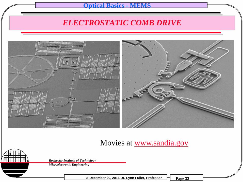
ELECTROSTATIC COMB DRIVE
Movies at www.sandia.gov

© December 20, 2016 Dr. Lynn Fuller, Professor
Optical Basics - MEMS
Page 33
Rochester Institute of Technology
Microelectronic Engineering
ELECTROSTATIC COMB DRIVE MIRROR
Movie

© December 20, 2016 Dr. Lynn Fuller, Professor
Optical Basics - MEMS
Page 34
Rochester Institute of Technology
Microelectronic Engineering
ELECTROSTATIC MIRROR
www.memsoptical.com

© December 20, 2016 Dr. Lynn Fuller, Professor
Optical Basics - MEMS
Page 35
Rochester Institute of Technology
Microelectronic Engineering
MIRRORS
MOEMs - Micro Optical Electro Mechanical Systems
Lucent Technologies –
Lambda router, 256 mirror fiber optic multiplexer

© December 20, 2016 Dr. Lynn Fuller, Professor
Optical Basics - MEMS
Page 36
Rochester Institute of Technology
Microelectronic Engineering
TORSION - MIRROR
Substrate
poly 1poly 0
Movable mirror
Inflectionpoint
Micro-mirror Perspective View
Torsion Hinge
© December 20, 2016 Dr. Lynn Fuller, Professor
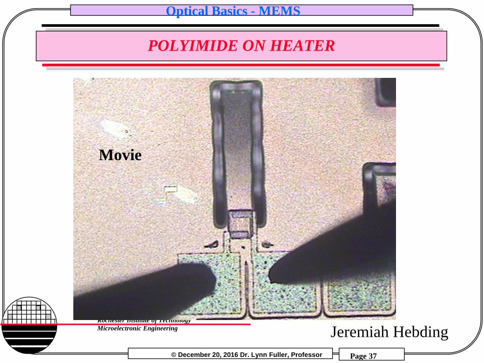
Optical Basics - MEMS
Page 37
Rochester Institute of Technology
Microelectronic Engineering
POLYIMIDE ON HEATER
Jeremiah Hebding
Movie

© December 20, 2016 Dr. Lynn Fuller, Professor
Optical Basics - MEMS
Page 38
Rochester Institute of Technology
Microelectronic Engineering
THERMALLY ACTUATED MEMS MICRO MIRROR

© December 20, 2016 Dr. Lynn Fuller, Professor
Optical Basics - MEMS
Page 39
Rochester Institute of Technology
Microelectronic Engineering
DIGITAL MIRROR LIGHT PROJECTION SYSTEM

© December 20, 2016 Dr. Lynn Fuller, Professor
Optical Basics - MEMS
Page 40
Rochester Institute of Technology
Microelectronic Engineering
TORSIONAL MIRRORS

© December 20, 2016 Dr. Lynn Fuller, Professor
Optical Basics - MEMS
Page 41
Rochester Institute of Technology
Microelectronic Engineering
TI MICROMIRROR PROJECTOR

© December 20, 2016 Dr. Lynn Fuller, Professor
Optical Basics - MEMS
Page 42
Rochester Institute of Technology
Microelectronic Engineering
TEXAS INSTRUMENTS DIGITAL PROJECTION PRODUCTS
www.TI.com
Movie

© December 20, 2016 Dr. Lynn Fuller, Professor
Optical Basics - MEMS
Page 43
Rochester Institute of Technology
Microelectronic Engineering
DXtreme PRO1
© December 20, 2016 Dr. Lynn Fuller, Professor
Optical Basics - MEMS
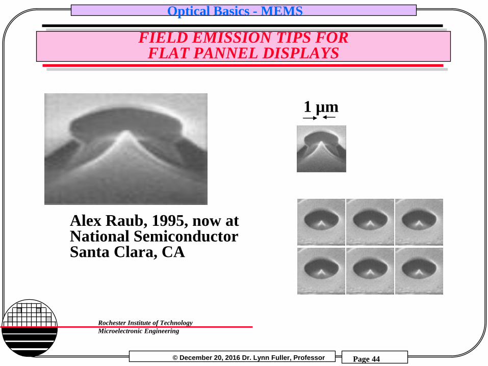
Page 44
Rochester Institute of Technology
Microelectronic Engineering
FIELD EMISSION TIPS FORFLAT PANNEL DISPLAYS
1 µm
Alex Raub, 1995, now atNational SemiconductorSanta Clara, CA

© December 20, 2016 Dr. Lynn Fuller, Professor
Optical Basics - MEMS
Page 45
Rochester Institute of Technology
Microelectronic Engineering
FIELD EMISSION FLAT PANNEL DISPLAYS
Substrate
Insulator
Vacuum Chamber
TransparentSi
O2 Window
EmitterControl Gate
Low Voltage Phosphor
Seal/Plug
Integrated Phosphor
Field Emission
Device
.900
.800
.700
.600
.500
.400
.300
.200
.100
000 .100 .200 .300 .400 .500 .600 .700 .800
GREEN
BLUISHGREEN
BLUE
BLUE
GREEN
PINK
PURPLISHRED
RED
REDDISHPURPLE
YELLOWISH
BLUEGREENISH
GREEN
Color Chart of AVT PhoshorsMicro-encapsulated Chamber
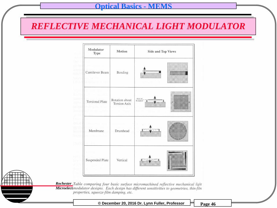
© December 20, 2016 Dr. Lynn Fuller, Professor
Optical Basics - MEMS
Page 46
Rochester Institute of Technology
Microelectronic Engineering
REFLECTIVE MECHANICAL LIGHT MODULATOR
© December 20, 2016 Dr. Lynn Fuller, Professor
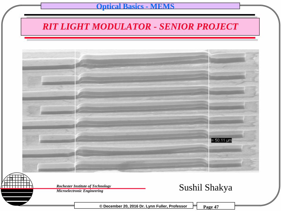
Optical Basics - MEMS
Page 47
Rochester Institute of Technology
Microelectronic Engineering
RIT LIGHT MODULATOR - SENIOR PROJECT
Sushil Shakya

© December 20, 2016 Dr. Lynn Fuller, Professor
Optical Basics - MEMS
Page 48
Rochester Institute of Technology
Microelectronic Engineering
REFERENCES
1. Micro Spectro Photometer by Marion Jess, Carl Duisberg
Gesellschaft e.V., Fachhochschule Koln, Germany , August 1996.
2. Fundamentals of Microfabrication, Marc Madou, CRC Press, LLC,
1997.
3. Scientific Measurement Systems, Inc., 2527 Foresight Circle, Grand
Junction, CO 81505-1007.
4. Micromachined Transducers, Gregory T. A. Kovacs, McGraw-Hill,
1998
5. Solar Cells, Martin A. Green, Prentice-Hall

© December 20, 2016 Dr. Lynn Fuller, Professor
Optical Basics - MEMS
Page 49
Rochester Institute of Technology
Microelectronic Engineering
HOMEWORK – OPTICAL BASICS FOR MEMS
1. If the human body is thought of as a black body light source.
What types of optical detector will be able to sense a human
by sensing its IR emission? Explain.
2. Look up the Texas Instruments Digital Light Projector
products. What is the cost of a developer kit for some of
their projection products.
3. Visit the following web sites and discuss one product of
interest for each. www.silicon-sensor.com
www.heimannsensor.com
www.oceanoptics.com
www.memsoptical.com


![Optical MEMS for Lightwave Communicationnanophotonics.eecs.berkeley.edu/Publications... · have focused on the development of optical MEMS devices and fabrication technologies [7]–[10].](https://static.fdocuments.in/doc/165x107/5f92c214e2beb91e807adccc/optical-mems-for-lightwave-commun-have-focused-on-the-development-of-optical-mems.jpg)