OPERATOR’S, ORGANIZATIONAL, DIRECT SUPPORT GENERAL …
260
TM 11-6625-1722-15 TECHNICAL MANUAL OPERATOR’S, ORGANIZATIONAL, DIRECT SUPPORT GENERAL SUPPORT, AND DEPOT MAINTENANCE MANUAL OSCILLOSCOPE AN/USM-273 (NSN 6625-00-930-6637) This copy is a reprint which includes current pages from Changes 1. HEADQUARTERS, DEPARTMENT OF THE ARMY JANUARY 1972
Transcript of OPERATOR’S, ORGANIZATIONAL, DIRECT SUPPORT GENERAL …

TM 11-6625-1722-15
TECHNICAL MANUAL
OPERATOR’S, ORGANIZATIONAL, DIRECT SUPPORT
GENERAL SUPPORT, AND DEPOT MAINTENANCE
MANUAL
OSCILLOSCOPE AN/USM-273(NSN 6625-00-930-6637)
This copy is a reprint which includes current
pages from Changes 1.
H E A D Q U A R T E R S , D E P A R T M E N T O F T H E A R M Y
JANUARY 1972

THIS MANUAL IS AN AUTHENTICATION OF THE MANU-FACTURER’S COMMERCIAL LITERATURE WHICH,THROUGH USAGE, HAS BEEN FOUND TO COVER THEDATA REQUIRED TO OPERATE AND MAINTAIN THISEQUIPMENT. SINCE THE MANIJAL WAS NOT PREPAREDIN ACCORDANCE WITH MILITARY SPECIFICATION, THEFORMAT HAS NOT BEEN STRUCTURED TO CONSIDERLEVEL OF MAINTENANCE NOR TO INCLUDE A FOR-MAL SECTION ON DEPOT MAINTENANCE STANDARDS.
W A R N I N G
DANGEROUS VOLTAGESEXIST IN THIS EQUIPMENT
DON’T TAKE CHANCES!
C A U T I O N
Special 3% silver solder is required on the ceramic terminalstrips in this equipment. A 40- to 75-watt soldering ironshould be used and it should be tinned with the same specialsolder. Additional quantities of the solder may be procuredunder FSN 3439-912-8698. Ordinary solder may be usedonly in dire emergency.

This Manual Contains Copyrighted Material ReproducedTektronix, Inc. All Rights Reserved
T ECHNICAL M A N U A L
By Permission Of
TM 11-6625-1722-15
HEADQUARTERSDEPARTMENT OF THE ARMY
NO. 11–6625–1722–15 WASHINGTON, D.C., 10 January 1972
Operator’s Organizational, Direct Support, General Support, and Depot
Maintenance Manual Including Repair Parts and Special Tools Lists
OSCILLOSCOPE AN/USM–273
S ECTION A.
1.
2.
3.
4.
5.
6.
7.
8.
9.
10,
APPENDIX A.
B.
C.
D.
INRODUCTION
CHARACTERISTICS
OPERATING INSTRUCTIONS . .. . . . . . . . . . . . . . . . . . . . .
CIRCUIT DESCRIPTION . . . . . . . . . . . . . . . . . .
MAINTENANCE
PERFOR0MANCE CHECK . . . . . . . . . . . . . . . . . . . . .
CALIBRATION
PREVENTIVE MAINTENANCE INSTRUCTIONS . . . . . . . . . . . . . . . . .
MECHNICAL PARTS IDENTIFICATION . . . . . . . . . . . . . . . . . . . . . . .
DIAGRAMS
RACKMOUNTING
REFERENCES
ITEMS COMPRISING AN OPERABLE EQUIPMENT . . . . . . . . . . . . . . . .
MAINTENANCE ALLOCATION . . . . . . . . . . . . . . .
REPAIR PARTS AND SPECIAL TOOLS LIST . . . . . . . . . . . . . .
Page
A-1
1-1
2–1
3–1
4–1
5-1
6–1
7–1
8-1
9-1
10-1
A–1
B–1
C-1
D-1


TM 11-6625-1722-15
Fig. 1-1. Top; the Type 453 Oscilloscope. Bottom; the Type R453 Oscilloscope.
A-O


TM 11-6625-1722-15
SECTION 0
INSTRUCTIONS
0-1. Scope
This manual describes Oscilloscope AN/USM-273 (fig. 1-1) and provides
maintenance instructions. Throughout this manual, the AN/USM-273 is re-
ferred to as the Tektronix Type 453 Oscilloscope. The maintenance allo-
cation chart appears in appendix C. Repair parts and special tools lists
are contained in TM-6625-1722-24P.
0-2. Indexes of Publications
a. DA Pam 310-4. Refer to the latest issue of DA Pam 310-4 to deter-
mine whether there are new editions, changes, or additional publications
pertaining to the equipment.
b . DA Pam 310-7. Refer to DA Pam 310-7 to determine whether there
are modification work orders (MWO’S) pertaining to the equipment.
0-3. Maintenance Forms, Records, and Reports
a. Reports of Maintenance and Unsatisfactory Equipment. Department
of the Army forms and procedures used for equipment maintenance will be
those prescribed by TM 38-750, The Army Maintenance Management System.
b. Report of Packaging and Handling Deficiencies. Fill out and for-
ward DD Form 6 (Packaging Improvement Report) as prescribed in AR 700-58/
NAVSUPINST 4030.29/AFR 71-13/MCO P4030.29A, and DLAR 4145.8.
c. Discrepancy in Shipment Report (DISREP) (SF 361). Fill out and
forward Discrepancy in Shipment Report (DISREP) (SF 361) as prescribed in
AR 55-38/NAVSUPINST 4610.33B/AFR 75-18/MCO P4610.19C and DLAR 4500.15.
0-1

TM 11-6625-1722-15
0-4. Reporting Equipment Improvement Recommendations (EIR)
If your Oscilloscope AN/USM-273 needs improvement, let us know. Send
us an EIR. You, the user, are the only one who can tell us what you
don’t like about your equipment. Let us know why you don’t like the
design. Tell us why a procedure is hard to perform. Put it on an SF 368
(Quality Deficiency Report). Mail it to Commander, US Army Communications
and Electronics Materiel Readiness Command, ATTN: DRSEL-ME-MQ, Fort
Monmouth, NJ 07703. We’ll send you a reply.
0-5. Administrative Storage
Administrative storage of equipment issued to and used by Army activi-
ties shall be in accordance with TM 740-90–1.
0-6 Destruction of Army Electronics Materiel
Destruction of Army electronics materiel to prevent enemy use shall be
in accordance with TM 750-244-2.
0-7. Reporting Errors and Recommending Improvements
You can help improve this manual. If you find any mistakes or if you
know of a way to improve the procedures, please let us know. Mail your
letter or DA Form 2028 (Recommended Changes to Publications and Blank
Forms) to Commander, US Army Communications and Electronics Materiel
Readiness Command, ATTN: DRSEL-ME-MQ, Fort Monmouth, NJ 07703. In
either case, a reply will be furnished direct to you.
0-2 Change 1

TM 11-6625-1722-15
SECTION 1
CHARACTERISTICS
In t roduct ion
The Tektronix Type 453 Oscilloscope is a transistorizedportable oscilloscope designed to operate in a wide rangeof environmental conditions. The light weight of the Type453 allows it to be easily transported, while providing theperformance necessary for accurate high-frequency meas-urements. The dual-channel DC-to-50 MHz vertical systemprovides calibrated deflection factors from 5 millivolts to10 volts/division. Channels 1 and 2 can be cascaded usingan external cable to provide a one millivolt minimum defect-ion factor (both VOLTS/DIV switches set to 5 mV).
The trigger circuits provide stable triggering over the fullrange of vertical frequency response. Separate trigger con-trols are provided to select the desired triggering for the Aand B sweeps. One of three sweep modes can be selectedfor the A sweep; automatic, normal or single sweep. Thehorizontal sweep provides a maximum sweep rate of 0.1microsecond/division (10 nanosecond/division using 10Xmagnifier) along with a delayed sweep feature for accuraterelative-time measurements. Accurate X-Y measurementscan be made with Channel 2 providing the vertical deflection,and Channel 1 providing the horizontal [deflection. (TRIGGERswitch set to CH 1 ONLY, HORIZ DISPLAY switch set to EXTHORIZ). The regulated DC power supplies maintain con-
stant output over a wide variation of line voltages and fre-quencies. Total power consumption of the instrument isapproximately 90 watts.
Information given in this instruction monual applies to theType R453 also unless otherwise noted. The Type R453 iselectrically identical to the Type 453 but is mechanicallyadapted for mounting in a standard 19-inch rack. Rack-mounting instructions, a mechanical parts list and a dimen-sional drawing for the Type R453 are provided in Section10 of this manual.
The electrical characteristics which follow are dividedinto two categories. Characteristics listed in the PerformanceRequirement column are checked in the Performance Checkand Calibration sections of this manual. Items listed in theOperational Information column are provided for referenceuse and do not directly reflect the measurement capabili-ties of this instrument. The Performance Check proceduregiven in Section 5 of this manual provides a convenientmethod of checking the items listed in the PerformanceRequirement column. The following electrical characteristics. .apply over a calibration interval of 1000 hours at an am-bient temperature range of -15°C to +55°C, except asotherwise indicated. Warm-up time for given accuracy is20 minutes.
ELECTRICAL CHARACTERISTICS
Characteristic
Deflection Factor
Deflection Accuracy
Variable Deflection Factor
Bandwidth at Upper -3 dBpoint (with or without P6010Probe)
20 mV to 10 VOLTS/DIV
10 mV/DIV
5 mV/DIV
Channels land 2 cascaded
Risetime (calculated). With orwithout P6010 Probe.20 mV to 10 VOLTS/DIV
10 mV/DIV
5 mV/DIV
Channels 1 and 2 cascaded
VERTICAL DEFLECTlON SYSTEM
Performance Requirement
5 millivolts/division to 10 volts/division in 11calibrated steps for each channel. One millivolt/division when Channel 1 and 2 are cascaded.
Within ±3Y% of indicated deflection with VARl-ABLE control set to CAL. Cascaded deflectionfactor uncalibrated.
Uncalibrated deflection factor at least 2.5 timesthe VOLTS/DIV switch indication. This providesa maximum uncalibrated deflection factor of 25volts/division in the 10 volts posit ion.
DC to 50 MHz or greater
DC to 45 MHz or greater
DC to 40 MHz or greater
DC to 25 MHz or greater
Less than 7 nanoseconds
Less than 7.8 nanoseconds
Less than 8.75 nanoseconds
Less than 14 nanoseconds
Operational Information
Steps in 1-2-5 sequence
With gain correct at 20 mV
Driven from 25-ohm source
Measured at one millivolt/division
Risetime calculated from bandwidthmeasurement using the formula:
Where:tr = Risetime in nanoseconds.
BW = Bandwidth in megahertz.
1-1

TM 11-6625-1722-15
VERTICAL (cont)
Characteristic
Input RC Characteristics
Performance Requirement
Maximum lnput Voltage
lnput Coupling Modes
AC Low-Frequency Response(lower -3 dB point)Without probe
With P6010 Probe
Trace Shift Due to Input GateCurrent (at 25°C)
Vertical Display Modes
Chopped Repetition Rate
Attenuator Isolation
Common Mode Rejection Ratio
Linear Dynamic Range Usefulfor Common-Mode Relectionin ADD Mode
Polarity Inversion
Signal Delay Line
Low-FrequencyVertical Linearity
Trace Drift (after 20 minutewarm up)20 mV to 10 VOLTS/DIV
10 mV/DIV
5 mV/DIV
gree C
Source
Coupling
Polarity
AC or DC, selected by front-panel switch
Negligible
Channel 1 onlyChannel 2 onlyDual-troce, alternate between channelsDual-trace, chopped between channelsAdded algebraically
Approximately one-microsecond segments fromeach channel dispiayed at repetition rate of 500kHz, ±20%.
Greater than 10,000:1, DC to 20 MHz
Greater than 20:1 at 20 MHz for common-modesignals less than eight times VOLTS/DIV switchsetting.
Signal on Channel 2 can be inverted
Less than 0.15 division compression or expansionof two division signal when positioned to verticalextremes of display area
TRIGGERING (A AND B SWEEP)
Internal from displayed channel or from Channel1 only
Internal from AC power sourceExternalExternal divide by 10
ACAC low-frequency rejectAC high-frequency rejectDC
Sweep can be triggered from positive-going ornegative-going portion of trigger signal
Operational Information
Typically 1 megohm (±2%), paralleledby 20 pF (±3%)
600 volts DC + peak AC (one kilohertzor less). Peak-to-peak AC not to exceed600 volts.
Typicaily 1.6 Hz, Input Coupling switchset to AC
Typically 0.16 Hz
With optimum GAINfrequency
adjustment at low
Less than 10% incremental signal dis-tortion for instantaneous input voltageof -10 or +10 t imes VOLTS/DIVswitch setting
Approximately 140 nanoseconds
Includes CRT linearity. Measured withone-kilohertz square wave.
Time Temperature
Typically less than Typically less than0.03 division/hour
Typically less than0.05 division/hour
Typically less than0.08 division/hour
0.0075 division/de-gree C
Typically less than0.0125 division/de-gree C
Typically less than0.02 division/de-
1 - 2

TM 11-6625-1722-15
TRIGGERING (cont)
Characteristic
Internal Trigger SensitivityAC
LF REJ
HF REJ
DC
External Trigger SensitivityAC
LF REJ
HF REJ
DC
Auto Triggering (A sweep only)
Single Sweep (A sweep only)
Display Jitter
Maximum Input Voltage
External Trigger Input RCCharacteristics (approximate)
LEVEL Control Range
Sweep RatesA Sweep
B sweep
Sweep Accuracy-A and BSweep5 s to 0.1 s /DIV
50 ms to 0.1 µs/DIV
Variable Sweep Rate
Performance Requirement
0.2 division of deflection, minimum, 30 Hz to 10MHz; increasing to 1 division at 50 MHz
0.2 division of deflection, minimum, 30 Hz to 100.2 division of deflection, minimum, 30 kHz to 10
0.2 division of deflection, minimum, 30 Hz to 50kHz
0.2 division of deflection, minimum, DC to 10MHz; increasing to 1 division at 50 MHz
50 millivolts, minimum, 30 Hz to 10 MHz; increas-ing to 200 millivolts at 50 MHz
50 millivolts, minimum, 30 kHz to 10 MHz; increas-ing to 200 millivolts at 50 MHz
50 millivolts, minimum, 30 Hz to 50 kHz
50 millivolts, minimum, DC to 10 MHz; increas-ing to 200 millivolts at 50 MHz
Stable display presented with signal amplitudesgiven under Internal and External Trigger Sensi-tivity above 20 Hz. Presents a free-running sweepfor lower frequencies or in absence of triggersignal.
A Sweep Generator produces only one sweepwhen triggered. Further sweeps are locked outuntil RESET button is pressed. Trigger sensitivitysame as given above.
Less than 1 nanosecond at 10 nanoseconds/divi-sion sweep rate (MAG switch set to X10)
At least ±2 volts, SOURCE switch in EXT posi-tion. At least ±20 volts, SOURCE switch in EXT÷10 position
HORIZONTAL DEFLECTION SYSTEM
A and B Sweep Generator
Operational Information
Typical -3 dB point, 16 Hz
Typical -3 dB point, 16 kHz
Typical -3 dB points, 16 Hz and 100kHz
Typical -3 dB point, 16 Hz
Typical -3 dB point, 16 kHz
Typical -3 dB points, 16 Hz and 100kHz
600 volts DC + peak AC (one kilohertzor less). Peak-to-peak AC not to exceed600 volts.
1 Megohm paralleled by 20 pF, exceptin LF REJ
0.1 microsecond/division to 5 seconds/division in24 calibrated stem
0.1 microsecond/division to 0.5 second/divisionin 21 calibrated steps
A sweep is main and delaying sweep
B sweep is delayed sweep
0°C to +40°C - 1 5 ° C t o + 5 5 ° C
With in ±3% of ind i - Wi th in ±5% of ind i -cated sweep rate cated sweep rate
A VARIABLE and B TIME/DiV VARl-
Wi th in ±3% of ind i - Wi th in ±4% of ind i -ABLE controls set to CAL
cated sweep rate cated sweep rate
Uncalibrated sweep rate to at least 2.5 times the TIME/DIV indication, or a maximum of at least12.5 seconds/division in the 5 s position (B sweep,maximum of 1.25 seconds/division in the .5 sposition.
1-3

TM 11-6625-1722-15
Characteristic
Sweep LengthA sweep
B sweep
S w e e p H o l d - o f f - A s w e e p5s to 10
A and B Sweep Generotor
Performance Requirement
Variable from less than 4 divisions to 11.0, ±0.5division
11.0 divisions, ±0.5 division
Less than one times the A TIME/DIV switch set-ting
Less than 2.5 microseconds
O p e r a t i o n a l I n f o r m a t i o n
A TIME/DIV switch set to 1 ms
B TIME/DIV switch set to 1 ms
Sweep Magnifier
Sweep Magnification Each sweep rate can be increased 10 times the Extends fastest sweep rate to 10 nano-indicated sweep rate by horizontally expanding seconds/divisionthe center division of display
Magnified Sweep Accuracy 1% tolerance added to speclfled sweep accuracy
Magnified Sweep Linearity ±1.5% for any eight division portion of thetotal magnified sweep length (excluding firstand last 60 nanoseconds of magnified sweep)
Normal/Magnified Registration ±0.2 division, or less, trace shift at graticuiecenter when switching MAG switch from X10to OFF
Sweep Delay
Calibrated Delay Time Range Continuous from 50 seconds to 1 microsecond A VARIABLE control set to CAL for indi-cated delay
DELAY-TIME MULTIPLIERDial Range 0.20 to 10.20
Delay Time Accuracy 0°C to +40°C -15° C to +55° C
5s to 0.1 s/DIV Within ±2.5% of indi- Within ±3.5% of indi-cated delay cated delay Includes incremental multiplier linearity
50 ms to 1 Within ±1.5% of indi- ‘Wi th in ±2% of indi -cated delay cated delay
Incremental Multiplier Linearity ±0.2% ±0.3%.Delay Time Jitter Less than 1 part in 20,000 of 10 times A TIME/ Equal to 0.5 division, or less, with the A
DIV switch setting TIME/DIV switch set to 1 ms and the BTIME/DIV switch set to 1
External Horizontal Amplifier
Input to Channel 1 (TRIGGERswitch in CH 1 ONLY)Deflection factor
Accuracy
X Bandwidth at Upper -3 dBPoint
Input RC characteristics
Phase difference between Xand Y amplifiers at 50 kHz
Input to EXT HORIZ ConnectorDeflection factor
5 millivolts/division to 10 volts/division in 11 cali-brated steps
0°C to +40°C
With in ±5% of ind i - Wi th in ±8% of ind i -cated deflection cated deflection
5 MHz or greater
Less than 3°
B SOURCE switch in EXT; 270 millivolts/division,±15%.B SOURCE switch in EXT± 2 0 %
Steps in 1-2-5 sequence.Channel 1 VARIABLE control does notaffect horizontal deflection
With external horizontal gain correctat 20 mV
Typically 1 megohm (±2%), paralleledby 20 pF (±3%)
1 - 4

TM 11-6625-1722-15
External Horizontal Amplifier (cont)
X Bandwidth at Upper -3 5 MHz or greater
Input RC characteristics(approximate]
Phase difference between Xand Y amplifiers at 50kHz
Waveshape
Polarity
Output Voltage
Output Current
Repetition Rate
Voltage Accuracy
Current Accuracy
Repetition Rate Accuracy
Risetime
Duty CycIe
Output Resistance
CALIBRATOR
Operational Information—
1 megohm, paralleled by 20 pF
Less than 3°
Square wave
Positive going with baseline at zero volts
0.1 volt or 1 volt, peak to peak Selected by CALIBRATOR switch on sidepanel
5-milliamperes through PROBE LOOP on side
.-± 1 . 5 %
±0.5%
Less than 1 microsecond
49% to 51%Approximately 200 ohms in 1 V position.Approximately 20 ohms in .1 V position.
Z AXIS INPUT
Sensitivity 5 volt peak-to-peak signal produces noticeablemodulation
Usable Frequency Range DC to greater than 50 MHz
Input Resistance at DC Approximately 47 kilohms
Input Coupling DC coupled
Polarity of Operation Positive-going input signal decreasestrace intensityNegative-going signal increases trace
Maximum Input Voltage 200 volts combined DC and peak AC
OUTPUT SIGNALS
A and B Gate—
Waveshape Rectangular pulse
Amplitude
Polarity Posltlve-going with baseline at about -0.7 volts.
Duration I Same duration as the respective sweep A GATE duration variable betweenabout 4 and 11 times the A TIME/DIV
I
Output resistanceVertical Signal Out (CH 1 only)
Output voltage 25 millivolts, or greater/division of CRT displayinto 1 megohm load.
Bandwidth DC to 25 MHz or greater when cascaded with Channel 2 or into 50-ohm load.
Output coupling D C c o u p l e d
Output resistance
switch setting with the A SWEEPLENGTH control.
Approximately 1.5 kilohms
Approximately 50 ohms
1 - 5

TM 11-6625-1722-15
Characteristic
Line Voltage
Voltage Ranges (AC, RMS)115-volts nominal
230-volts nominal
Line Frequency
Maximum Power Consumptionat 115 Volts, 60 Hz
POWER SUPPLY
Performance Requirement
115 volts nominal or 230 volts nominal
90 to 110 volts104 to 126 volts112 to 136 volts
180 to 220 volts208 to 252 volts224 to 272 volts— — —48 to 440 Hz
Operational Information.—
Line voltage and range selected by LineVoltage Selector assembly on rearpanel. Voltage ranges apply for wave-form distortion which does not reducethe peak line voltage more than 5%below the true sine-wave peak value.
92 watts (105 volt-amperes)
CATHODE-RAY TUBE (CRT)
Tube Type Tektronix T4530-31-1 rectangularIPhosphor P31 standard. Others available on
Accelerating Potential
special order.
Approximately 10 kV total (cathodepotential -1.95 kV).
GraticuleT y p e Internal
Area Six divisions vertical by 10 divisions horizontal.Each division equals 0.8 centimeter.
Illumination Variable edge lighting
Unblinking Bias-type, DC coupled to CRT grid.
Raster Distortion 0.1 division or less total Adjustable with Geometry and Y AxisAl ign adjustments.
T r a c e F i n d e r Limits display within graticule area when pressed.
E N V I R O N M E N T A L C H A R A C T E R I S T I C S
The following environmental test limits apply when tested in accordance with the recom-mended test procedure. This instrument will meet the electrical characteristics given in thissection following environmental test. Complete details on environmental test procedures,including failure criteria, etc., may be obtained from Tektronix, Inc. Contact your localTektronix Field Office or representative.
Characteristic
TemperatureOperating
Non-operating
AltitudeOperating
Non-operating
HumidityNon-operating
VibrationOperating andnon-operating
ShockOperating andnon-operating
Performance Requirement
- 1 5 ° C t o + 5 5 ° c
- 5 5 ° t o + 7 5 ° C
15,000 feet maximum
50,000 feet maximum
Five cycles (120 hours) of Mil-Std-202C, Method106B
15 minutes along each of the three major axesat a total displacement of 0.025-inch peak to peak(4 g at 55 c/s) with frequency varied from 10-55-10 c/s in one-minute cycles. Hold at 55 c/s forthree minutes on each axis.
Two shocks of 30 g, one-half sine, 11 millisecondduration each direction along each major axis.
Supplemental Information
Fan at rear circulates air throughout ins-trument. Automatic resetting thermalcutout protects instrument from over-heating.
Derate maximum operating tempera-ture by 1°C/1000 feet change in altitudeabove 5000 feet.
Exclude freezing and vibration
Instrument secured to vibration platformduring test. Total vibration time, about55 minutes.
Guillotine-type shocks.Total of 12 shocks
1 - 6

Characteristic
Transportation
Package vibration
Package dropType 453
Type R453
TM 11-6625-1722-15
ENVIRONMENTAL CHARACTERISTICS (cont)
Performance Requirement
Meets National Safe Transit type of test whenpackaged as shipped from Tektronix, Inc.One hour vibration slightly in excess of 1 g.
30-inch drop on any corner, edge or flat surface.
18-inch drop on any corner, edge or flat surface.
M E C H A N I C A L C H A R A C T E R I S T I C S
Characteristic Information
ConstructionChassis Aluminum alloy
Panel Aluminum alloy with ano-dized finish
Cabinet Blue vinyl-coated aluminum
Circuit boards Glass-epoxy laminateOverall Dimensions, Type
453 (measured ot maxi-mum points)Height
Width
Length
handle positioned for carry-ing.
Overall Dimensions, TypeR453 (measured at maxi-mum points)
W i d t h
Operational Information
Package should just leave vibration sur-face
Length
ConnectorsZ AXIS INPUT
All other connectors
Net WeightType 453 (includes front
cover without accessor-ies)
Type R453 (without ac-cessories)
19 inches
panel;
Binding post
BNC
Approximately 29 pounds.
Approximately 32 pounds.
S T A N D A R D A C C E S S O R I E S
Standard accessories supplied with the Type 453 and R453are listed on the last pullout page of the Mechanical PartsList illustrations.
He ight 7 inches
1 - 7


TM 11-6625-1722-15
SECTION 2
OPERATING INSTRUCTIONS
G e n e r a l
TO effectively use the Type 453, the operation and capa-bilities of the instrument must be known. This section de-scribes the operation of the front-, side- and rear-panelcontrols and connectors, gives first time and general operat-ing information and lists some basic applications for thisinstrument.
F r o n t C o v e r a n d H a n d l e
The front cover furnished with the Type 453 provides adust-tight seal around the front panel. Use the cover toprotect the front panel when storing or transporting theinstrument. The cover also provides storage space for probesa n d o t h e r a c c e s s o r i e s ( s e e F i g . 2 - 1 ) .
Fig. 2-1. Accessory storage provided in front cover.
The handle af the Type 453 can be positioned for carryingor as a tilt-stand for the instrument. To position the handle,press in at both pivot points (see Fig. 2-2) and turn thehandle to the desired position. Several positions are pro-vided for convenient carrying or viewing. The instrumentmay also be set an the rear-panel feet for operation orstorage.
O p e r a t i n g V o l t a g e
The Type 453 can be operated from either a 115-volt ora 230-volt nominal line-voltage source. The Line Voltage
Fig. 2-2. Handle positioned to provide a stand for the instrument
Selector assembly on the rear panel converts the instrumentfrom one operating range to the other. In addition, thisassembly changes the primary connections of the powertransformer to allow selection of one of three regulatingranges. The assembly also includes the two line fuses. Whenthe instrument is converted from 115-volt to 230-volt nominaloperation, or vice versa, the assembly connects or discon-nects one of the fuses to provide the correct protection forthe instrument. Use the following procedure to convert thisinstrument between nominal line voltages or regulatingranges.
1. Disconnect the instrument from the power source.
2. Loosen the two captive screws which hold the coveronto the voltage selector assembly; then pull to remove thecover.
3. To convert from 115-volts nominal to 230-volts nomi-nal line voltage, pull out the Voltage Selector switch bar(see Fig. 2-3]; turn it around 180° and plug it back into theremaining holes. Change the line-cord power plug to matchthe power-source receptacle or use a 115- to 230-voltadapter.
4. To change regulating ranges, pull out the RangeSelector switch bar (see Fig. 2-3); slide it to the desiredposition and plug it back in. Select a range which is cen-tered about the average line voltage to which the instru-ment is to be connected (see Table 2-1).
5. Re-install the cover and tighten the two captive screws.
6. Before applying power to the instrument, check thatthe indicating tabs on the switch bars are protruding throughthe correct holes for the desired nominal line voltage andregulating range.
2 - 1

TM 11-6625-1722-15
more frequently. The air filter should be cleaned occasion-
Fig. 2-3. Line Voltage Selector assembly on the rear panel (shownwith cover removed).
CAUTION
The Type 453 should not be operated with theVoltage Selector or Range Selector switches in thewrong pos i t ions for the l ine vo l tage appl ied.Operation of the instrument with the switches inthe wrong posit ions may either provide incorrectaperotion or damage the instrument.
TABLE 2-1
O p e r a t i n g T e m p e r a t u r e
The Type 453 is cooled by air drawn in at the rear andblown out through holes in the top and bottom covers. Ade-quate clearance on the top, bottom and rear must be pro-vided to allow heat to be dissipated away from the instru-ment. The clearance provided by the feet at the bottom andrear should be maintained. If possible, allow about oneinch of clearance on the top. Do not block or restrict the airflow from the air-escape holes in the cabinet.
A thermal cutout in this instrument provides thermal pro-tection and disconnects the power to the instrument if theinternal temperature exceeds a safe operating level. Opera-tion of the instrument for extended periods without the coversmay cause it to overheat and the thermal cutout to open
ally to aIIOW the maximum amount of cooling air to enterthe instrument. Cleaning instructions are given in Section 4.
The Type 453 can be operated where the ambient airtemperature is between -15°C and +55°C. Derate themaximum operating temperature 1°C for each additional1000 feet of altitude above 5000 feet. This instrument canbe stored in ambient temperatures between –55°C and+75°C. After storage at temperatures beyond the operatinglimits, allow the chassis temperature to come within theoperating limits before power is applied.
R a c k m o u n t i n g
Complete information for mounting the Type R453 in acabinet rack is given in Section 10 of this manual.
C O N T R O L S A N D C O N N E C T O R S
A brief description of the function or operationfront-, side- and rear-panel controls and connectors(see Fig. 2-4). More detailed information is givensection under General Operating Information.
Cathode-Ray Tube
INTENSITY
FOCUS
SCALE ILLUM
TRACE FINDER
Vertical (both
VOLTS/DIV
VARIABLE
UNCAL
POSITION
GAIN
Input Coupling(AC GND DC)
o f t h efollowsin this
Controls brightness of display.
Provides adjustment for a well-defined dis-play.
Controls graticule illumination.
Compresses display within graticule areaindependent of display position or appli-ed signals.
channels except as noted)
Selects vertical deflection factor (VARl-ABLE control must be in CAL position forindicated deflection factor).
Provides continuously variable deflectionfactor between the calibrated settings ofthe VOLTS/DIV switch.
Light indicates that the VARIABLE controlis not in the CAL position.
Controls vertical position of trace.
Screwdriver adjustment to set gain of theVertical Preamp. Line between adjust-ment and 20 mV VOLTS/DIV position in-dicates that gain should be set withVOLTS/DIV switch in this position.
Selects method of coupling input signalto Vertical Deflection System.
AC: DC component of input signal isblocked. Low frequency l imit -3 dBpoint) is about 1.6 hertz.
GND: Input circuit is grounded (does notground applied signal).
2 - 2

TM 11-6625-1722-15
Fig. 2-4. Front-, side- and rear-panel controls and connectors.
2 - 3

TM 11-6625-1722-15
DC: All components of the input signal arepassed to the Vertical Deflection System.
STEP ATTEN Screwdriver adjustment to balance Verti-B A L cal Deflection System in the 5, 10 and 20
mV positions of the VOLTS/DIV switch.
INPUT Vertical input connector for signal.
MODE Selects vertical mode of operation.
CH 1: The Channel 1 signal is displayed.
CH 2: The Channel 2 signal is displayed.
ALT: Dual trace display of signal on bothchannels. Display switched at end ofeach sweep.
CHOP: Dual trace display of signal onboth channels. Approximately one-mi-crosecond segmerlts from each channeldisplayed at a repetition rate of about500 kilohertz.
ADD: Channel 1 and 2 signals are alge-braically added and the algebraic sumis displayed on the CRT.
TRIGGER Selects saurce of internal trigger signalf r o m v e r t i c a l s y s t e m .
NORM: Sweep circuits triggered from dis-played channel(s). Channel 1 signalavailable at CH 1 OUT connector.
CH 1 ONLY: Sweep circuits triggered onlyfrom signal applied to the Channel 1INPUT connector. No signal availableat CH 1 OUT connector. CH 1 lights,located beside A and B SOURCE switch-es indicate when the TRIGGER switch isin the CH 1 ONLY position.
INVERT (CH 2 Inverts the Channel 2 signal when pulledonly) out.
A and B Triggering (both where applicable)
EXT TRIG Input connector for external trigger signal.INPUT Connector in B Triggering section of front
panel also serves as external horizontalinput when HORIZ DISPLAY switch is inEXT HORIZ position and B SOURCE switchis in EXT position.
SOURCE Selects source of trigger signal.
INT: Internal trigger signal obtained fromVertical Deflection System. When CH1 light is on, trigger signal is obtainedonly from the Channel 1 input signal;when the light is off, the trigger signalis abtained from the displayed chan-nel(s). Source of internal trigger signalis selected by the TRIGGER switch.
LINE: Trigger signal obtained from a sam-ple of the line voltage applied to thisinstrument.
EXT: Trigger signal obtained from an ex-ternal signal applied to the EXT TRIGINPUT connector.
Attenuates external trigger sig-nal approximately 10 times.
CH 1 Light indicates that the internal trigger sig-nal is abtained only from the signal con-nected to the Channel 1 INPUT connector(see TRIGGER switch).
COUPLING Determines method of coupling triggersignal to trigger circuit.
AC: Rejects DC and attenuates signals be-low about 30 hertz. Accepts signalsbetween abaut 30 hertz and 50 mega-hertz.
LF REJ: Rejects DC and attenuates signalsbelow about 30 kilohertz. Accepts sig-nals between about 30 kilohertz and 50megahertz.
HF REJ: Accepts signals between about 30hertz and 50 kilohertz; rejects DC andattenuates signals outside the aboverange.
DC: Accepts all trigger signals from DC to50 megahertz or greater.
SLOPE Selects portion of trigger signal whichstarts the sweep.
+: Sweep can be triggered from positive-going portion of trigger signal.
-: Sweep can be triggered from negative-going portion of trigger signal.
LEVEL Selects amplitude point on trigger signalat which sweep is triggered.
HF STAB Decreases display jitter for high-frequency(A Trigger- signals. Has negligible effect at lowering only) sweep rates.
A and B Sweep
DELAY-TIMEMULTIPLIER
A SWEEPTRIG’D
UNCAL AOR B
A AND BTIME/DIVAND DELAYTIME
Provides variable sweep delay between0.20 and 10.20 times the delay time indi-cated by the A TIME/DIV switch.
Light indicates that A sweep is triggeredand will produce a stable display withcorrect INTENSITY and POSITION controlsettings.
Light indicates that either the A or BVARIABLE control is not in the CAL posi-tion.
A TIME/DIV switch (clear plastic flange)selects the sweep rate of the A sweepcircuit for A sweep only operatian andselects the basic delay time (to be multi-plied by DELAY-TIME MULTIPLIER dialsetting) for delayed sweep operation.B TIME/DIV (DELAYED SWEEP) switchselects sweep rate of the B sweep circuit
2 - 4
2-5
TM 11-6625-1722-15
A VARIABLE
B SWEEPMODE
HORIZDISPLAY
M A G
A SWEEPMODE
for delayed sweep operation only. VARl-ABLE controls must be in CAL positions forcalibrated sweep rates.
Provides continuously variable A sweeprate to at least 2.5 times setting of theA TIME/DIV switch. A sweep rate is cali-brated when control is set fully clockwiseto CAL.
Selects B sweep operation mode.
TRIGGERABLE AFTER DELAY TIME: Bsweep circuit will not produce a sweepuntil a trigger pulse is received follow-ing the delay time selected by theDELAY TIME (A TIME/DIV) switch andthe DELAY-TIME MULTIPLIER dial.
B STARTS AFTER DELAY TIME: B sweepcircuit runs immediately following delaytime selected by the DELAY TIME switchand DELAY-TIME MULTIPLIER dial.
Selects horizontal mode of operation.
A: Horizontal deflection provided by Asweep. B sweep inoperative.
A INTEN DURING B: Sweep rate deter-mined by A TIME/DIV switch. An inten-sified portion appears on the sweepduring the B sweep time. This positionprovides a check of the duration andposition of the delayed sweep (B) withrespect to the delaying sweep (A).
DELAYED SWEEP (B): Sweep rate deter-mined by B TIME/DIV switch with thedelay time determined by the setting ofthe DELAY TIME (A TIME/DIV) switchand the DELAY-TIME MULTIPLIER dial.Sweep mode determined by B SWEEPMODE switch.
EXT HORIZ: Horizontal deflection pro-vided by an external signal.
Increases sweep rate to ten times settingof A or B TIME/DIV switch by horizontallyexpanding the center division of the dis-play. Light indicates when magnifier ison.
Determines the operating mode for Asweep.
AUTO TRIG: Sweep initiated by the ap-plied trigger signal using the A Trig-gering controls when the trigger signalrepetition rate is above about 20 hertz.For lower repetition rates or when thereis no trigger signal, the sweep free runsat the sweep rate selected by the ATIME/DIV switch to produce a brightreference trace.
NORM TRIG: Sweep initiated by the ap-plied trigger signal using the A Trig-gering controls. No trace is displayedwhen there is no trigger signal.
RESET
A SWEEPLENGTH
POSITION
FINE
1 kHz CAL
POWER ON
Side Panel
ASTIG
B TiME/DIV-VARIABLE
PROBE LOOP
A GATE
B GATE
CH 1 OUT
SINGLE SWEEP: After a sweep is display-ed, further sweeps cannot be presenteduntil the RESET button is pressed. Dis-play is triggered as for NORM opera-tion using the A Triggering controls.
When the RESET button is pressed (SIN-GLE SWEEP mode), a single display willbe presented (with correct triggering) whenthe next trigger pulse is received. RESETlight (inside RESET button) remains onuntil a trigger is received and the sweep iscompleted. RESET button must be pressedbefore another sweep can be presented.
Adiusts length of A sweep. In the FULLposition (clockwise detent), the sweep isabout 11 divisions long. As the control isrotated counterclockwise, the length of Asweep is reduced until it is less than fourdivisions long iust before the detent inthe fully-counterclockwise position is reach-ed. In the B ENDS A position (counter-clockwise detent), the A sweep is resetat the end of the B sweep to provide thefastest possible sweep repetition rate fordelayed sweep displays.
Controls horizontal position of trace.
Provides more precise horizontal positionadjustment.
Calibrator output connector.
Light: Indicates that POWER switch ison and the instrument is connected toa line voltage source.
Switch: Controls power to the instrument.
Screwdriver adjustment used in conjunc-tion with the FOCUS control to obtain awell-defined display. Does not requirereadjustment in normal use.
Provides continuously variable sweep rateto at least 2.5 times setting of B TIME/DIVswitch. B sweep rate is calibrated whencontrol is set fully clockwise to CAL.
Current loop providing five-milliamperesquare-wave current from calibrator cir-cuit.
Output connector providing a rectangularpulse coincident with A sweep.
Output connector providing a rectangularpulse coincident with B sweep.
Output connector providing a sample ofthe signal applied to the Channel 1 lN-PUT connector when the TRIGGER switchis in the NORM position.

TM 11-6625-1722-15
CALIBRATOR
TRACEROTATION
Rear Panel
Z AXIS INPUT
Line VoltageSelector
Switch selects output voltoge of Calibrator.1-volt or 0.1-volt square wave available.
Screwdriver adjustment to align trace withhorizontal graticule lines.
Input connector for intensity modulationof the CRT display.
Switching assembly to select the nominaloperating voltage and the line voltagerange. The assembly also includes theline fuses.
Voltage Selector: Selects nominal operat-ing voltage range (115V or 230V).
Range Selector: Selects line voltage range(low, medium, high).
FIRST-TIME OPERATION
The following steps will demonstrate the use of the con-trols and connectors of the Type 453. It is recommendedthat this procedure be followed completely for familiariza-tion with this instrument.
Setup Information
1. Set the front-panel controls as follows:
CRT Controls
INTENSITY Counterclockwise
FOCUS Midrange
SCALE ILLUM Counterclockwise
Vertical Controls (both channels if applicable)
VOLTS/DIV 20 mV
VARIABLE CAL
POSITION Midrange
INPUT COUPLING D C
MODE CH 1
TRIGGER NORM
INVERT Pushed in
Triggering Controls (both A and B if applicable)
LEVEL Clockwise (+)
SLOPE +
COUPLING AC
SOURCE INT
Sweep Controls
DELAY-TIME 0.20MULTIPLIER
A and B TIME/DIV .5 ms
A VARIABLE CAL
B SWEEP MODE B STARTS AFTERDELAY TIME
2 - 6
HORIZ DISPLAY
MAG
POSITION
A SWEEP LENGTH
A SWEEP MODE
POWER
Side-Panel Controls
B TIME/DIV VARIABLE
CALIBRATOR
A
OFF
Midrange
FULL
AUTO TRIG
OFF
CAL
.1 V
2. Connect the Type 453 to a power source that meetsthe voltage and frequency requirements of the instrument.If the available line voltage is outside the limits of the LineVoltage Selector assembly position (on rear panel), seeOperating Voltage in this section.
3. Set the POWER switch to ON. Allow about five minuteswarmup so the instrument reaches a normal operating tem-perature before proceeding.
CRT Controls
4. Advance the INTENSITY control until the trace is atthe desired viewing level (near midrange).
5. Connect the 1 kHz CAL connector to the Channel 1INPUT connector with a BNC cable.
6. Turn the A LEVEL control toward 0 until the displaybecomes stable. Note that the A SWEEP TRIG’D light is onwhen the display is stable.
7. Adiust the FOCUS control for a sharp, well-defineddisplay over the entire trace length. (If focused display can-not be obtained, see Astigmatism Adjustment in this section.)
8. Disconnect the input signal and move the trace withthe Channel 1 POSITION control so it coincides with one ofthe horizontal graticule lines. If the trace is not parallel withthe graticule line, see Trace Alignment Adjustment in thissection.
9. Rotate the SCALE ILLUM control throughout its rangeand notice that the graticule lines are illuminated as thecontrol is turned clockwise (most obvious with mesh or smoke-gray filter installed). Set control so graticule lines areilluminated as desired.
Vertical Controls
10. Change the CH 1 VOLTS/DIV switch from 20 mV to 5mV. If the vertical position of the trace shifts, see StepAttenuator Balance in this section.
11. Set the CH 1 VOLTS/DIV switch to 20 mV and set theChannel 1 Input Coupling switch to AC. Connect the 1 kHzCAL connector to both the Channel 1 and 2 INPUT con-nectors with two BNC cables and a BNC T connector.
NOTE
If the BNC cables and BNC T connector are notavailable, make the following changes in the pro-cedure. Place the BNC jack post (supplied ac-cessory) on the 1 kHz CAL connector and connect

TM 1 1 - 6 6 2 5 - 1 7 2 2 - 1 5
the Channel 1 and 2 INPUT connectors. Connectthe probe tips to the BNC jack post. Set the CALI-BRATOR switch (on side-panel) to 1 V.
12. Turn the Channel 1 POSITION control to center thedisplay. The display is a square wave, five divisions inamplitude with about five cycles displayed on the screen. Ifthe display is not five divisions in amplitude, see VerticalGain Adjustment in this section.
13. Set the Channel 1 Input Coupling switch to GND ondposition the trace to the center horizontal line.
14. Set the Channel 1 Input Coupling switch to DC. Notethat the baseline of the waveform remains at the centerhorizontal line (ground reference).
15. Set the Channel 1 Input Coupling switch to AC. Notethat the waveform is centered about the center horizontall i n e .
16. Turn the Channel 1 VARIABLE control throughout itsrange. Note that the UNCAL light comes on when the VARl-ABLE control is moved from the CAL position (fully clock-wise). The deflection should be reduced to about two divi-sions. Return the VARIABLE control to CAL.
17. Set the MODE switch to CH 2.
18. Turn the Channel 2 POSITION control to center thedisplay. The display will be similar to the previous displayfor Channel 1. Check Channel 2 step attenuator balance andgain as described in steps 10 through 12. The Channel 2input Coupling switch and VARIABLE control operate asdescribed in steps 13 through 16.
19. Set both VOLTS/DIV switches to 50 mV.
20. Set the MODE switch to ALT and position the Channel1 waveform to the top of the graticule area and the Chan-nel 2 waveform to the bottom of the graticule area. Turnthe A TIME/DIV switch throughout its range. Note that thedisplay alternates between channels at all sweep rates.
21. Set the MODE switch to CHOP and the A TIME/DIVNote the switching between channels as
shown by the segmented trace. Set the TRIGGER switch toCH 1 ONLY; the trace should appear more solid, since it isno longer triggered on the between-channel switching trans-ients. Turn the A TIME/DIV switch throughout its range. Adual-trace display is presented at all sweep rates, but unlikeALT, both channels are displayed on each trace on a time-sharing basis. Return the A TIME/DIV switch to .5 ms.
22. Set the MODE switch to ADD. The display should befour divisions in amplitude. Note that either POSITION con-trol moves the display.
23. Pull the INVERT switch. The display is a straight lineindicating that the algebraic sum of the two signals is zero(if the Channel 1 and 2 gain is correct).
24. Set either VOLTS/DIV switch to 20 mV. The square-wave display indicates that the algebraic sum of the twosignals is no longer zero. Return the MODE switch to CH 1and both VOLTS/DIV switches to .2 (if using 10X probes,set both VOLTS/DIV switches to 20 mV). Push in the INVERTswitch.
Triggering
25. Set the CALIBRATOR switch to 1 V. Rotate the A LEVELcontrol throughout its range. The display free runs at theextremes of rotation. Note that the A SWEEP TRIG'D lightis on only when the display is triggered.
26. Set the A SWEEP MODE switch to NORM TRIG. Againrotate the A LEVEL control throughout its range. A displayis presented only when correctly triggered. The A SWEEPTRIG'D light operates as in AUTO TRIG. Return the A SWEEPMODE switch to AUTO TRIG.
27. Set the A SLOPE switch to -. The trace starts on thenegative part of the square wave. Return the switch to +;the trace starts with the positive part of the square wave.
28. Set the A COUPLING switch to DC. Turn the Chan-nel 1 POSITION control until the display becomes unstable(only part of square wave visible). Return the A COUPLINGswitch to AC; the display is again stable. Since changingtrace position changes DC level, this shows how DC levelchanges affect DC trigger coupling. Return the display tothe center of the screen.
29. Set the MODE switch to CH 2; the display should bestable. Remove the signal connected to Channel 1; the dis-play free runs. Set the TRIGGER switch to NORM; the dis-play is again stable. Note that the CH 1 lights in A and BTriggering go out when the TRIGGER switch is changed toNORM.
30. Connect the Calibrator signal to both the Channel 2INPUT and A EXT TRIG INPUT connectors. Set the ASOURCE switch to EXT. Operation of the LEVEL, SLOPEand COUPLING controls for external triggering are the sameas described in steps 25 through 28.
31. Set the A SOURCE switch to EXTis the same as for EXT. Note that the A LEVEL control hasless range in this position, indicating trigger signal attenua-tion. Return the A SOURCE switch to INT.
32. Operation of the B Triggering controls is similar toA Triggering.
Normal and Magnified Sweep
33. Set the A TIME/DIV switch to 5 ms and the MAGswitch to X10. The display should be similar to that obtain-ed with the A TIME/DIV switch set to .5 ms and the MAGswitch to OFF.
34. Turn the horizontal POSITION control throughout itsrange; it should be possible to position the display acrossthe complete graticule area. Now turn the FINE control. Thedisplay moves a smaller amount and allows more precisepositioning. Return the A TIME/DIV switch to .5 ms, theMAG switch to OFF and return the start of the trace to theleft graticule line.
Delayed Sweep
36. Pull the DELAYED SWEEP knob out and turn it to 50(DELAY TIME remains at .5 ms). Set the HORIZ DISPLAY
switch to A INTEN DURING B. An intensified portion, aboutone division in length, should be shown at the start of thetrace. Rotate the DELAY-TIME MULTIPLIER dial throughoutits range; the intensified portion should move along the dis-play.
2 - 7

2-8
TM 11-6625-1722-15
37. Set the B SWEEP MODE switch to TRIGGERABLEAFTER DELAY TIME. Again rolate the DELAY-TIME MULTI-PLIER dial throughout its range and note that the intensifiedportion appears to jump between posltive slopes of the dis-play. Set the B SLOPE switch to -; the intensified portionbegins on the negative slope. Rotate the B LEVEL control;the intensified portion of the display disappears when the BLEVEL control is out of the trlggerable range. Return theB LEVEL control to 0.
38. Set the HORIZ DISPLAY switch to DELAYED SWEEP(B). Rotate the DELAY-TIME MULTIPLIER dial througout itsrange; about one-half cycle of the waveform should bedisplayed on the screen (Ieading edge visible only at highINTENSITY control setting). The display remains stable onthe screen, indicating that the B sweep is triggered.
39. Set the B SWEEP MODE switch to B STARTS AFTERDELAY TIME. Rotate the DELAY-TIME MULTIPLIER dialthroughout its range; the display moves continously acrossthe screen as the control is rotated.
40. Rotate the DELAYTIME MIULTIPLIER dial fully counter-clockwise and set the HORIZ DISPLAY switch to A INTENDURING B. Rotate the A SWEEP LENGTH control counter-clockwise; the Iength of the display decreases. Set the con-trol to the B ENDS A position; now the display ends afterthe intensified portion. Rotate the DELAY-TIME MULTIPLIERdial ond note that the sweep length increases as the displaymoves across the screen. Return the A SWEEP LENGTH con-trol to FULL and the HORIZ DISPLAY switch to A.
48. Reduce the INTENSITY control setting to normal, BSOURCE switch to INT and set the HORIZ DISPLAY switcht o A .
Z-Axis Input
Single Sweep
41. Set the A SWEEP MODE switch to SINGLE SWEEP.Remove the Calibrator signal from the Channel 2 INPUTconnector. Press the RESET button; the RESET light shouldcome on and remain on. Again apply the signal to the Chan-nel 2 INPUT connector; a single trace should be presentedand the RESET light should go out. Return the A SWEEPMODE switch to AUTO TRIG.
External Horizontal
42. Connect the Calibrator signal to both the Channel 2INPUT and EXT HORIZ (B EXT TRIG lNPUT] connectors. Setthe B SOURCE switch to EXT, B COUPLING switch to DCand the HORIZ DISPLAY switch to EXT HORIZ. lncrease theINTENSITY control setting until the display is visible (two dotsdisplayed diagonally). The display should be five divisionsvertically and about 3.7 divisions horizontally. Set the B
10. The display should be reducedten times horizontally. The display can be positioned hori-zontally with the horizontal POSITION or FINE control andvertically with the Channel 2 POSITION control.
43. Connect the Calibrator signal to both the Channel 1and 2 INPUT connectors. Set the TRIGGER switch to CH 1ONLY and the B SOURCE switch to INT.
44. The display should be five divisions vertically andhorizontally. The display can be postioned horizontallywith the Channel 1 POSITION control and vertically with theChannel 2 POSITION control.
Trace Finder
46. Set the CH 1 and CH 2 VOLTS/DlV switches to 10mv. The display iS not visible since it exceeds the scan areaof the CRT.
47. Press the TRACE FINDER button. Note that the dis-play is returned to the display area. While holding theTRACE FINDER button depressed, increase the vertical andhorizontal deflection factors until the display is reduced toabout two divisions vertically ond horizontally. Adjust theChannel 1 and 2 POSITION controls to center the displayabout the center lines of the graticule. Release the TRACEFINDER and note that the display remains within the viewingarea. Disconnect the applied signal.
49. If an, External signal is available (five volts peak topeak minimum] the function of tlhe Z AXIS INPUT circuit canbe demonstrated. Connect the external signal to both theChannel 2 INPUT connector and the Z AXIS INPUT bindingposts. Set the A TIME/DIV switch to display about fivecycles of the waveform. The positive peaks of the waveformshould be blanked and the negative peaks intensified, indi-cating intensify modulation.
50. This completes the basic operating procedure for theType 453. lnstrument operation not explained here, or opera-tions which need further explanation are discussed underGeneral Operating Information.
CONTROL SETUP CHART
Fig. 2-5 shows the front, side and rear panels of the Type453. This chart can, be reproduced and used as a test-setuprecord for special measurements, applications or procedures,or it may be used as a training aid for familiarization withthis instrument.
G E N E R A L O P E R A T I N G I N F O R M A T I O N
Intensi fy Control
The setting of the INTENSITY control may affect the cor-rect focus of the display. Slight readjustment of the FOCUScontrol may be necessary when the intensity level is changed.To protect the CRT phosphor, do not turn the INTENSITYcontrol higher than necessary to provide a satisfactory dis-play. The light filters reduce the observed light output fromthe CRT. When using these filters, avoid odvancing theINTENSITY control to a setting that may bum the phosphor.When Ihe highest intensity display is desired, remove thefilters and use the clear faceplate protector. Also, be care-ful that the INTENSITY control is not set too high whenchanging the TIME/DlV switch front a fast to a slow sweeprate, or when changing the HORIZ DISPLAY switch from EXTHORIZ operation to the norrmal sweep mode.
45. Change the CH1 VOLTS/DIV switch to 5. The displayplay is reduced to two divisions horizontally. Now set theCH 2 VOLTS/DIV switch to 5. The display is reduced to twodivisions vertically.
Astigmatism Adjustment
If a well-defined trace cannot be obtained with the FOCUScontrol, adjust the ASTIG adjustment (side panel) as fol-lows.

TM 11-6625-1722-15
Fig. 2-5. Control setup chart for the Type 453.
2 - 9

TM 11-6625-1722-15
NOTE
To check for proper setting of the ASTIG adjust-ment, slowly turn the FOCUS control through theoptimum setting. If the ASTIG adjustment is cor-rectly set, the vertical and horizontal portionsof the trace will come into sharpest focus at thesame position of the FOCUS control. This settingof the ASTIG adjustment should be correct for anydisplay. However, it may be necessary to resetthe FOCUS control slightly when the INTENSITYcontrol is changed.
1. Connect a 1 V Calibrator signal to either channel andset the VOLTS/DIV switch of that channel to present a two-division display. Set the MODE switch to display the chan-nel selected.
2. Set the TIME/DIV switch to .2 ms
3. With the FOCUS control and ASTIG adjustment set tomidrange, adjust the INTENSITY control so the rising portionof the display can be seen.
4. Set the ASTIG adjustment so the horizontal and verti-cal portions of the display are equally focused, but notnecessarily well focused.
5. Set the FOCUS control so the vertical portion of thetrace is as thin as possible.
6. Repeat steps 4 and 5 for best overall focus. Make finalcheck at normal intensity.
Grat icu le
The graticule of the Type 453 is internally marked on thefaceplate of the CRT to provide accurate, no-parallax meas-urements. The graticule is marked with six vertical and 10horizontal divisions. Each division is 0.8 centimeter square.In addition, each major division is divided inta five minordivisions at the center vertical and horizontal lines. Thevertical gain and horizontal timing are calibrated to thegraticule so accurate measurements can be made from theCRT. The illumination of the graticule lines can be variedwith the SCALE ILLUM control.
Fig. 2-6 shows the graticule of the Type 453 and definesthe various measurement lines. The terminology defined herewill be used in all discussions involving graticule measure-ments.
T r a c e A l i g n m e n t A d j u s t m e n t
If a free-running trace is not parallel to the horizontalgraticule lines, set the TRACE ROTATION adjustment as fol-lows. Position the troce to the center horizontal line. Adjustthe TRACE ROTATION adjustment (side panel) so the traceis parallel with the horizontal graticule lines.
L ight F i l ter
The mesh filter provided with the Type 453 provides shield-ing against radiated EMI (electro-magnetic interference) fromthe face of the CRT. It also serves as a light filter to makethe trace more visible under ambient light conditions. To
Fig. 2-6. Definition of measurement lines on Type 453 graticule.
remove the filter, press down at the bottom of the frameand pull the top of the filter away from the CRT faceplate(see Fig. 2-7).
The tinted light filter minimizes light reflections from theface of the CRT to improve contrast when viewing the dis-play under high ambient light conditions. A clear plasticfaceplate protector is also provided with this instrument foruse when neither the mesh nor the tinted filter is used. Theclear faceplate protector provides the best display for wave-form photographs. It is also preferable for viewing highwriting rate displays.
A filter or the faceplate protector should be used at alltimes ta protect the CRT faceplate from scratches. The face-plate protector and the tinted filter mount in the same holder.
Fig. 2-7. Removing the filter or faceplate protector.
2 - 1 0

TM 11-6625-1722-15
To remove the light filter or faceplate protector from theholder, press it out to the rear. They can be replaced bysnapping them back into the holder.
T race F inder
The TRACE FINDER provides a means af locating a displaywhich overscans the viewing area either vertically or hori-zontally. When the TRACE FINDER button is pressed, thedisplay is compressed within the graticule area. TO locateand reposition an overscanned display, use the followingprocedure.
1. Press the TRACE FINDER button.
2. While the TRACE FINDER button is held depressed,increase the vertical and horizontal deflection factors untilthe vertical deflection is reduced to about two divisions andthe horizontal deflection is reduced to about four divisions(the horizontal deflection needs to be reduced only when inthe external horizontal mode of operation).
3. Adjust the vertical and horizontal POSITION controlsto center the display about the vertical and horizontal cen-ter lines.
4. Release the TRACE FINDER button; the display shouldremain within the viewing area.
Vert ical Channel Se lect ion
Either of the input channels can be used for single-tracedisplays. Apply the signal to the desired INPUT connectorand set the MODE switch to display the channel used. How-ever, since CH 1 ONLY triggering is provided only in Chan-nel 1 and the invert feature only in Channel 2, the correctchannel must be selected to take advantage of these fea-tures. For dual-trace displays, connect the signals to bothINPUT connectors and set the MODE switch to one of thedual-trace positions.
V e r t i c a l G a i n A d j u s t m e n t
To check the gain of either channel, set the VOLTS/DIVswitch to 20 mV. Set the CALIBRATOR switch to .1 V andconnect the 1 kHz CAL connector to the INPUT of the chan-nel used. The vertical deflection should be exactly fivedivisions. If not, adjust the front-panel GAIN adjustmentfor exactly five divisions of deflection.
NOTE
If the gain of the two channels must be closelymatched (such as for ADD mode operation), theADJUSTMENT procedure given in the Calibrationsection should be used.
The best measurement accuracy when using probes is pro-vided if the GAIN adjustment is made with the probes in-stalled (set the CALIBRATOR switch to 1 V). Also, to providethe most accurate measurements, calibrate the vertical gainof the Type 453 at the temperature at which the measurementis to be made.
S t e p A t t e n u a t o r B a l a n c e
To check the step attenuator balance of either channel,set the Input Coupling switch to GND and set the A SWEEP
MODE swich to AUTO TRIG to provide a free-running trace.Change the VOLTS/DIV switch from 20 mV to 5 mV. If thetrace moves vertically, adjust the front-panel STEP ATTENBAL adjustment as follows (allow at least 10 minutes warmup before performing this adjustment].
1. With the Input Coupling switch set to GND and theVOLTS/DIV switch set to 20 mV, move the trace to the centerhorizontal line of the graticule with the vertical POSITIONcontrol.
2. Set the VOLTS/DIV switch to 5 mV and adjust theSTEP ATTEN BAL adjustment to return the trace to the centerhorizonal line.
3. Recheck step attenuator balance and repeat adjustmentuntil no trace shift occurs as the VOLTS/DIV switch is chang-ed from 20 mV to 5 mV.
S ignal Connect ions
In general, probes offer the most convenient means of con-necting a signal to the input of the Type 453. The Tektronixprobes are shielded to prevent pickup of electrostatic inter-ference. A 10X attenuator probe offers a high input imped-ance and allows the circuit under test to perform very closeto normal operating conditions. However, a 10X probealso attenuates the input signal 10 times. The TektronixP6045 Field Effect Transistor probe and accessory powersupply offer the same high-input impedance as the 10Xprobes. However, it is particularly useful since it provideswide-band operatian while presenting no attenuation (1Xgain) and a low input capacitance. To obtain maximumbandwidth when using the probes, observe the groundingconsiderations given in the probe manual. The probe-to-connector adapters and the bayonet-ground tip provide thebest frequency response. Remember that a ground straponly a few inches in length can produce several percent ofringing when operating at the higher frequency limit of thissystem. See your Tektronix, Inc. catalog for characteristicsand compatibility of probes for use with this system.
In high-frequency applications requiring maximum overallbandwidth, use coaxial cables terminated at both ends intheir characteristic impedance. See the discussion on coax-ial cables in this section for more information.
High-level, low-frequency signals can be connected directlyto the Type 453 INPUT connectors with short unshieldedleads. This coupling method works best for signals belowabout one kilohertz and deflection foctors above one volt/division. When this method is used, establish a commonground between the Type 453 and the equipment under test.Attempt to position the leads away from any source of inter-ference to avoid errors in the display. If interference isexcessive with unshielded leads, use a coaxial cable or aprobe.
L o a d i n g E f f e c t o f t h e T y p e 4 5 3
As nearly as possible, simulate actual operating condi-tions in the equipment under test. Otherwise, the equipmentunder test may not produce a normal signal. The 10Xattenuator probe and field effect transistor probe mentionedpreviously offer the least circuit loading. See the probeinstruction manual for loading characteristics of the indivi-dual probes.
2 - 1 1

TM 11-6625-1722-15
When the signal is coupled directly to the input of theType 453, the input impedance is about one megohmparalleled by about 20 pF. When the signal is coupled tothe input through a coaxial cable, the effeclive input ca-pacitance depends upon the type and Iength of cable used.See the following discussion for inforrnation on obtainingmaximum frequency responspe with coaxial cables.
The signal cables used to connect the signal 10 the type453 INPUT connectors have a Iarge effect on the accuracyof the displayed high-frequency waveform. To maitain thehigh-frequency characteristics of the applied signal, high-quality low-loss coaxial cable should be used. The cableshould be terminated at the Type 453 INPUT connector in itscharacteristic impedonce. If it is necessary to use cableswith differing characteristic impedances, use suitable imped-ance-matching devices to provide the correct transition, withminimum loss, from one impedance to the other.
The characteristic impedance, velocity of propagation andnature of signal lOSSeS in a coaxial cable are determinedby the physical and electrical characteristics of the cable.Losses caused by energy dissipation in the dielectric areproportional to the signal frequency. Therefore, much ofthe high-frequency information in a fast-rise pulse can belost in only a few feet of interconnecting cable if it is notthe correct type. To be sure of the high-frequency responseof the system when using cables longer than about five feet,observe the transient response of the Type 453 and theinterconnecting cable with a fast-rise pulse generator (gen-erator risetime Iess than 0.5 nanoseconds).
Input Coupl ing
The Channel 1 and 2 lnput Coupling switches allow achoice of input caupling. The type of display desired willdetermine the coupling used.
The DC position can be used for most applications. How-ever, if the DC component of the signal is much larger thanthe AC component, the AC position vvill probably provide abetter display. DC coupling should be used to display ACsignals below about 16 heltz as they will be attenuated inthe AC position.
In the AC position, the DC component of the signal isblocked by a capacitor in the input circuit. The low-fre-quency response in the AC position is about 1.6 hertz (–3 dBpoint). Therefore, some low-frequency distortion can beexpected near this frequency limit. Distortion will alsoappear in square waves which have low-frequency com-ponents.
The GND position provides a ground reference at theinput of the Type 453. The signal applied to the input con-nector is internally disconnected but not grounded. Theinput circuit is held at ground potential, eliminating the needto externally ground the input to establish a DC groundreference.
The GND position can also be used to pre-charge thecoupling capacitor to the average voltage level of the signalapplied to the INPUT connector. This allows measurementof only the AC component of signals having both AC and
DC components. The pre-charging network incorporatedin this unit aIIOWS the input-coupling capacitor to charge tothe DC source voltage level when the Input Coupling switchis set to GND. The procedure for using this feature is asfollows:
1. Before connecting the signal containing a DC compo-nent to the Type 453 INPUT connector, set the Input Couplingswitch to GND. Then connect the signal to the INPUTconnector.
2. Wait about one second for the coupling capacitor tocharge.
3. Set the Input Coupling switch to AC. The trace (dis-play) will remain on the screen and the AC component ofthe signal can be measured in the normal manner.
Def lect ion Factor
The amount of vertical deflection produced by a signalis determined by the signal amplitude, the attenuation factorof the probe (if used), the setting of the VOLTS/DIV switchand the setting of the VARIABLE VOLTS/DIV control. Thecalibrated deflection factors indicated by the VOLTS/DIVswitches apply only when the VARIABLE control is set tothe CAL position.
The VARIABLE VOLTS/DIV control provides variable(uncalibrated) vertical deflection between the calibratedsettings of the VOLTS/DIV switch. The VARIABLE controlextends the maximum vertical deflection factor of the Type453 to at least 25 volts/division (10 volts position).
Dual-T race Operat ion
Alternate Mode. The ALT position of the MODE switchproduces a disploy which alternates between Channel 1 and2 with each sweep of the CRT. Although the ALT modecan be used at all sweep rates, the CHOP mode providesa more satisfactory display at sweep rates below about 50microseconds/division. At these slower sweep rates, alternatemode switching becomes visually perceptible.
Proper internal triggering in the ALT mode can be ob-tained in either the NORM or CH 1 ONLY positions of theTRIGGER switch. When in the NORM position, the sweep istriggered from the signal on each channel. This provides astable display of two unrelated signals, but does not indicatethe time relationship between the signals. In the CH 1 ONLYposition, the two signals are displayed showing true timerelationship. If the signals are not time related, the Channel2 waveform will be unstable in the CH 1 ONLY position.
Chopped Mode. The CHOP position of the MODE switchproduces a display which is electronically switched betweenchannels. In general, the CHOP mode provides the bestdisplay at sweep rates slower than about 50 microseconds/division, or whenever dual-trace, single-shot phenomena areto be displayed. At faster sweep rates the chopped switch-ing becomes apparent and may interfere with the display.
Proper internal triggering for the CHOP mode is providedwith the TRIGGER switch set to CH 1 ONLY. If the NORMposition is used, the sweep circuits are triggered from thebetween-channel switching signal and both waveforms will
2 - 1 2

TM 11-6625-1722-15
be unstable. External triggering provides the same result asCH 1 ONLY triggering.
Two signals which are time-related can be displayed inthe chopped mode showing true time relationship. If thesignals are not time-related, the Channel 2 display willappear unstable. Two single-shot, transient, or randomsignals which occur within the time interval determined bythe TIME/DIV switch (10 times sweep rate) can be comparedusing the CHOP mode. To correctly trigger the sweep formaximum resolution, the Channel 1 signal must precede theChannel 2 signal. Since the signals show true time relation-ship, time-difference measurements can be made.
C h a n n e l 1 O u t p u t a n d C a s c a d e d O p e r a t i o n
If a lower deflection factor than provided by the VOLTS/DIV switches is desired, Channel 1 can be used as a wide-band preamplifier for Channel 2. Apply the input signal tothe Channel 1 INPUT connector. Connect a 50-ohm BNCcable (18-inch or shorter cable for maximum cascaded fre-quency response) between the CH 1 OUT (side panel) andthe Channel 2 INPUT connectors. Set the MODE switch toCH 2 and the TRIGGER switch to NORM. With both VOLTS/DIV switches set to 5 mV, the deflection factor will be lessthan one millivolt/division.
To provide calibrated one millivolt/division deflectionfactor, connect the .1 volt Calibrator signal to the Channel 1INPUT connector. Set the CH 1 VOLTS/DIV switch to .1and the CH 2 VOLTS/DIV switch to 5 mV. Adjust the Chan-nel 2 VARIABLE VOLTS/DIV control to produce a displayexactly five divisions in amplitude. The cascaded deflectionfactor is determined by dividing the CH 1 VOLTS/DIV switchsetting by 5 (CH 2 VOLTS/DIV switch and VARIABLE controlremain as set above). For example, with the CH 1 VOLTS/DIV switch set to 5 mV the calibrated deflection factor willbe 1 millivolt/division; CH 1 VOLTS/DIV switch set to 10 mV,2 millivolts/division, etc.
The following operating considerations and basic appli-cations may suggest other uses for this feature.
1. If AC coupling is desired, set the Channel 1 InputCoupling switch to AC and leave the Channel 2 InputCoupling switch set to DC. When both Input Couplingswitches are set to DC, DC signal coupling is provided.
2. Keep both vertical POSITION controls set near mid-range. If the input signal has a DC level which necessitatesone of the POSITION controls being turned away frommidrange, correct operation can be obtained by keepingthe Channel 2 POSITION control near midrange and usingthe Channel 1 POSITION control to position the trace nearthe desired locatian. Then, use the Channel 2 POSITIONcontrol far exact positioning. This method will keep bothInput Preamps operating in their linear range.
3. The output voltage at the CH 1 OUT connectar is atleast 25 millivolts/division of CRT display in all CH 1 VOLTS/DIV switch positions.
4. The MODE switch and Channel 1 VARIABLE VOLTS/DIV control have no effect on the signal available at theCH 1 OUT connector.
5. The Channel 1 Input Preamp can be used as an imped-ance matching stage with or without voltage gain. The
input resistance is one megohm and the output resistance isabout 50 ohms.
6. The dynamic range of the Channel 1 Input Preamp isequal to about 20 times the CH 1 VOLTS/DIV setting. TheCH 1 OUT signal is nominally at 0 volt DC for a 0 volt DCinput level [Channel 1 POSITION control centered). TheChanel 1 POSITION control can be used to center the out-put signal within the dynamic range of the amplifier.
7. If dual-trace operation is used, the signal applied tothe Channel 1 INPUT connector is displayed when Channel1 is turned on. When Channel 2 is turned on, the amplifiedsignal is displayed. Thus, Channel 1 trace can be used tomonitor the input signal while the amplified signal is dis-played by Channel 2.
8. In special applications where the flat frequency re-sponse of the Type 453 is not desired, a filter insertedbetween the CH 1 OUT and Channel 2 INPUT connectorallows the oscilloscope to essentially take on the frequencyresponse of the filter. Combined with method 7, the input canbe monitored by Channel 1 and the filtered signal displayedby Channel 2.
9. By using Channel 1 as a 5X low-level voltage pre-amplifier (5 mV position), the Channel 1 signal availableat the CH 1 OUT connector can be used for any applicationwhere a low-impedance preamplifier signal is needed.Remember that if a 50-ohm load impedance is used, thesignal amplitude will be about one-half.
Algebraic Addi t ion
General. The ADD position of the MODE switch can beused to display the sum or difference of two signals, forcommon-mode rejection to remove an undesired signal or forDC offset (applying a DC voltage to one channel to offsetthe DC component of a signal on the other channel).
The common-mode rejection ratio of the Type 453 isgreater than 20:1 at 20 megahertz for signal amplitudes upto eight times the VOLTS/DIV switch setting. Rejection ratiosof 100:1 can typically be achieved between DC and 5 mega-hertz by careful adjustment of the gain of either channelwhile observing the displayed common-mode signal.
Deflection Factor. The overall deflection in the ADDposition of the MODE switch when both VOLTS/DIV switchesare set to the same position is the same as the deflectionfactor indicated by either VOLTS/DIV switch. The ampli-tude of an added mode display can be determined directlyfrom the resultant CRT deflection multiplied by the deflec-tion factor indicated by either VOLTS/DIV switch. How-ever, if the CH 1 and CH 2 VOLTS/DIV switches are set todifferent deflection factors, resultant voltage is difficult todetermine from the CRT display. In this case, the voltageamplitude of the resultant display can be determined accu-rately only if the amplitude of the signal applied to eitherchannel is known.
Precautions. The following generalbe observed when using the ADD mode.
1. Do not exceed the input voltage453.
precautions should
rating of the Type
2 - 1 3

TM 11-6625-1722-15
2. Do not apply signals that exceed on equivalent ofabout 20 times the VOLTS/DIV switch setting. For example,with a VOLTS/DIV switch setting of .5, the voltage appliedto that channel should not exceed about 10 volts. Largervoltages may distort the display.
3. Use vertical POSITION control settings which mostnearly position the signal of each channel to mid-screenwhen viewed in either the CH 1 or CH 2 positions of theMODE switch. This insures the greatest dynamic range forADD mode operation.
4. For similiar response from each channel, set both InputCoupling switches to the same position.
T r igger Source
INT. For most applications, the sweep can be triggeredinternally. In the INT position of the Triggering SOURCEswitch, the trigger signal is obtained from the VerticalDeflection System. The TRIGGER switch provides furtherselection of the internal trigger signal; obtained from theChannel 1 signal in the CH 1 ONLY position, or from thedisplayed signal when in the NORM position. For single-trace displays of either channel, the NORM position pro-vides the most convenient operation. However, for dual-trace displays special considerations must be made to providethe correct display. Set Dual-Trace Operation in this sectionfor dual-trace triggering information.
LINE. The LINE position of the SOURCE switch connectsa sample of the power-line frequency to the Trigger Gen-erator circuit. Line triggering is useful when the input signalis time-related to the line frequency. It is also useful forproviding a stable display of a line-frequency componentin a complex waveform.
EXT. An external signal conected to the EXT TRIG INPUTconnector can be used to trigger the sweep in the EXTposition of the Triggering SOURCE switch. The external sig-nal must be time-related to the displayed signal for a stabledisplay. An external trigger signal can be used to providea triggered display when the internal signal is too low inamplitude for correct triggering, or contains signal com-ponents on which it is not desired to trigger. It is also usefulwhen signal tracing in amplifiers, phase-shift networks, wave-shaping circuits, etc. The signal from a single point in thecircuit under test can be connected to the EXT TRIG INPUTconnector through a signal probe or cable. The sweep isthen triggered by the same signal at all times and allowsamplitude, time relationship or waveshape changes ofsignals at various points in the circuit to be examined with-out resetting the trigger controls.
same as described for EXT except that the external triggeringsignal is attenuated 10 times. Attenuation of high-amplitudeexternal triggering signals is desirable to broaden the rangeof the Triggering LEVEL control. When the COUPLINGswitch is set to LF REJ, attenuation is about 20:1.
T r igger Coupl ing
Four methods of coupling thecircuits can be selected withswitches. Each position permits
trigger signal to the triggerthe Triggering COUPLINGselection or rejection of the
frequency components of the trigger signal which can triggerthe sweep.
AC. The AC position blocks the DC component of thetrigger signal. Signals with low-frequency components belowabout 30 hertz are attenuated. In general, AC coupling canbe used for most applications. However, if the trigger signalcontains unwanted components or if the sweep is to betriggered at a low repetition rate or a DC level, one of theremaining COUPLING switch positions will provide a betterdisplay.
The triggering point in the AC position depends on theaverage voltage level of the trigger signal. If the triggersignals occur in a random fashion, the average voltage levelwill vary, causing the triggering point to vary also. This shiftof the triggering point may be enough so it is impossible tomaintain a stable display. In such cases, use DC coupling.
LF REJ. In the LF REJ position, DC is rejected and signalsbelow about 30 kilohertz are attenuated. Therefore, thesweep will be triggered only by the higher-frequency com-ponents of the signal. This position is particularly usefulfor providing stable triggering if the trigger signal containsline-frequency components. Also, in the ALT position of theMODE switch, the LF REJ position provides the best displayat high sweep rates when comparing two unrelated signals(TRIGGER switch set to NORM).
HF REJ. The HF REJ position passes all low-frequencysignals between about 30 hertz and 50 kilohertz. DC isrejected and signals outside the given range are attenuated.When triggering from complex waveforms, this position isuseful for providing stable display of low-frequency compo-nents.
DC. DC coupling can be used to provide stable triggeringwith low-frequency signals which would be attenuated inthe AC position, or with low-repetition rate signals. TheLEVEL control can be adjusted to provide triggering at thedesired DC level on the waveform. When using internaltriggering, the setting of the Channel 1 and 2 POSITIONcontrols affects the DC trigger level.
DC trigger coupling should not be used in the ALT dual-trace mode if the TRIGGER switch is set to NORM. If used,the sweep will trigger on the DC level of one trace and theneither lock out completely or free run on the other trace.Correct DC triggering for this mode can be obtained withthe TRIGGER switch set to CH 1 ONLY.
T r i g g e r S l o p e
The triggering SLOPE switch determines whether the triggercircuit responds on the positive-going or negative-goingportion of the trigger signal. When the SLOPE switch is inthe + (positive-going) position, the display starts with thepositive-going portion of the waveform; in the - (negative-going) position, the display starts with the negative-goingportion of the waveform (see Fig. 2-8]. When several cyclesof a signal appear in the display, the setting of the SLOPEswitch is often unimportant. However, if only a certainportion of a cycle is to be displayed, correct setting of theSLOPE switch is important to provide a display which startson the desired slope of the input signal.
2 - 1 4

2-15
TM 11-6625-1722-15
Fig. 2-8. Effects of Triggering LEVEL control and SLOPE switch.

TM 11-6625-1722-15
T r i g g e r L e v e l
The Triggering LEVEL control determines the voltage levelon the trigger signal at which the sweep is triggered. Whenthe LEVEL control is set in the + region, the trigger circuitresponds at a more positive point on the trigger signal.When the LEVEL control is set in the - region, the triggercircuit responds at a more negative point on the triggersignal. Fig. 2-8 illustrates this effect with different settingsof the SLOPE switch.
To set the LEVEL control, first select the TriggeringSOURCE, COUPLING and SLOPE. Then set the LEVELcontrol fully counterclockwise ond rotate it clockwise untilthe display starts at the desired point.
High-F requency S tabi l i ty
The HF STAB control (A only) is used to provide a stabledisplay of high-frequency signals. If a stable display cannotbe obtained using the A LEVEL control (trigger signal musthave adequate amplitude), adjust the HF STAB control forminimum horizontal jitter in the display. This control haslittle effect with low-frequency signals.
A S w e e p T r i g g e r e d L i g h t
The A SWEEP TRIG’D Iight provides a convenient indica-tion of the condition of the A Triggering circuit. If the ATriggering controls are correctly adjusted with an adequatetrigger signal applied, the light is on. However, if the ALEVEL control is misadjusted, the A COUPLING or ASOURCE switches incorrectly set or the trigger signal toolow in omplitude, the A SWEEP TRIG’D light will be off.This feature can be used as a general indication of correcttriggering. It is particularly useful when setting up thetrigger circuits when a trigger signal is available without atrace displayed on the CRT and it alSo indicates that the Asweep is correctly triggered when operating in the DELAYEDSWEEP (B) mode.
A S w e e p M o d e
AUTO TRIG. The AUTO TRIG position of the A SWEEPMODE switch provides a stable display when the A LEVELcontrol is correctly set (see Trigger Level in this section] anda trigger signal is available. The A SWEEP TRIG’D lightindicates when the A Sweep Generator is triggered.
When the trigger repetition rate is less then about 20hertz, or in the absence of an adequate trigger signal, theA Sweep Generator free runs to produce a reference trace.When an adequate trigger signal is again applied, thefree-running condition ends and the A Sweep Generator istriggered to produce a stable display (with correct A LEVELcontrol setting.)
NORM TRIG. Operation in the NORM TRIG positionwhen a trigger signal is applied is the same as in the AUTOTRIG position. However, when a trigger signal is not present,the A Sweep Generator remains off and there is no display.The A SWEFP TRIG’D light indicates when the A sweep istriggered. The NORM TRIG mode can be used to display
signals with repetition rates below about 20 hertz. This modeprovides an indication of an adequate trigger signal as wellas the correctness of trigger control settings, since there isno display without proper triggering. Also, the A SWEEPTRIG’D light is off when the A sweep is not correctlytriggered.
SINGLE SWEEP. When the signal to be displayed is notrepetitive or varies in amplitude, shape or time, a conven-tional repetitive display may produce an unstable presenta-tion. To avoid this, use the single-sweep feature of the Type453. The SINGLE SWEEP mode can also be used to photo-graph a non-repetitive signal.
To use the SINGLE SWEEP mode, first make sure thetrigger circuit will respond to the event to be displayed.Set the A SWEEP MODE switch to AUTO TRIG or NORMTRIG and obtain the best possible display in the normalmanner (for random signals set the trigger circuit to triggeron a signal which is approximately the same omplitude andfrequency as the random signal). Then, set the A SWEEPMODE switch to SINGLE SWEEP and press the RESET button.When the RESET button is pushed, the next trigger pulseinitiates the sweep and a single trace will be presented onthe screen. After this sweep is complete, the A Sweep Gen-erator is "locked out" until reset. The RESET light locatedinside the RESET button lights when the A Sweep Generatorcircuit has been reset and is ready to produce a sweep;it goes out after the sweep is complete. To prepare thecircuit for another single-sweep display, press the RESETbutton again.
Select ing Sweep Rate
The A AND B TIME/DIV switches select calibrated sweeprates for the Sweep Generators. The A and B VARIABLEcontrols provide continuously variable sweep rates betweenthe settings of the TIME/DIV switches. Whenever the UNCALA OR B light is on, the sweep rate of either A or B SweepGenerator, or both, is uncalibrated. The light is off whenthe A VARIABLE (front panel) and B TIME/DIV VARIABLE(side panel) controls are both set to the CAL position.
The sweep rate of the A Sweep Generator is bracketedby the two black lines on the clear plastic flange of theTIME/DIV switch (see Fig. 2-9). The B Sweep Generatorsweep rate is indicated by the dot on the DELAYED SWEEPknob. When the dot on the outer knob is set to the sameposition as the lines on the inner knob, the two knobs locktogether and the sweep rate of both Sweep Generators ischanged at the same time. However, when the DELAYEDSWEEP knob is pulled outward, the clear plastic flange isdisengaged and only the B Sweep Generator sweep rate ischanged. This allows changing the delayed sweep ratewihout changing the delay time determined by the A SweepGenerator.
When making time measurements from the graticule, thearea between the first-division and ninth-division vertical linesprovides the most linear time measurement (see Fig. 2-10).Therefore, the first and last division of the display should notbe used for making accurate time measurements. Positionthe start of the timing area to the first-division vertical lineand set the TIME/DIV switch so the end of the timing areafalls between the first- and ninth-division vertical lines.
2 - 1 6

Fig. 2-9.
TM 1 1 - 6 6 2 5 - 1 7 2 2 - 3 5
Sweep Magnification
The sweep magnifier expands the sweep ten times. Thecenter division of the unmagnified display is the portionvisible on the screen in mognified form (see Fig. 2-11]. Equiv-alent length of the magnified sweep is about 100 divisions;any 10 division portion may be viewed by adjusting thehorizontal POSITION control to bring the desired portiononto the viewing area. The FINE position control is particu-larly useful when the magnifier is on, as it provides position-ing in small increments for more precise control.
To use the magnified sweep, first move the portion of thedisplay which is to be expanded to the center of the grati-cule. Then set the MAG switch to X10. The FINE positioncontrol can be adjusted to position the magnified display
Fig. 2-10. Area of graticule used for accurate time measurements.
Fig. 2-11. Operation of sweep magnifier.
as desired. The light located below the MAG switch is onwhenever the magnifier is on.
When the MAG switch is set to X10, the sweep rate isdetermined by dividing the TIME/DIV switch setting by 10.For example, if the TIME/DIV switch is set tomagnified sweep rate is 0.05 microsecond/division. Themagnified sweep rate must be used for all time measure-ments when the MAG switch is set to X10. The magnifiedsweep rate is calibrated when the UNCAL A OR B lightis off.
Delayed Sweep (B)
The delayed sweep (B sweep) is operable in the A INTENDURING B and DELAYED SWEEP (B) positions of the HORIZDISPLAY switch. The A sweep rate along with the DELAY-TIME MULTIPLIER dial setting determines the time that theB sweep is delayed. Sweep rate of the delayed portion isdetermined by the B TIME/DIV (DELAYED SWEEP) switchsetting.
In the A INTEN DURING B position, the display willappear similar to Fig. 2-12A. The amount of delay timebetween the start of A sweep and the intensified portion isdetermined by the setting of the A TIME/DIV switch and theDELAY-TIME MULTIPLIER dial.
For example, the delay indicated by the DELAY-TIMEMULTIPLIER dial setting shown in Fig. 2-13 is 3.55; this cor-responds to 3.55 CRT divisions of A sweep. This readingmultiplied by the setting of the A TIME/DIV switch givesthe calibrated delay time before the start of the B sweep(see B Sweep Mode which follows). The intensified portionof the display is produced by the B sweep. The length of
2 - 1 7

TM 1 1 - 6 6 2 5 - 1 7 2 2 - 1 5
F i g . 2 - 1 2 . ( A ) A I N T E N D U R I N G B d i s p l a y ( D E L A Y - T I M E M U L T I -PLIER, 2.95; A TIME/DIV, .5 ms; B TIME/DIV, 50 ps), ( B ) D E L A Y E DSWEEP (B) d i sp lay.
this portion is about 10 times the setting of the B TIME/DIVswitch.
When the HORIZ DISPLAY switch is set to DELAYEDSWEEP (B), only the intensified portion as viewed in the AINTEN DURING B position is displayed on the screen atthe sweep rate indicated by the B TIME/DIV switch (seeFig. 2-12B).
F i g . 2 - 1 3 . D E L A Y - T I M E M U L T I P L I E R d i a l . R e a d i n g s h o w n : 3 . 5 5 .
2 - 1 8
B SWEEP MODE. The B SWEEP MODE switch providestwo modes of delayed sweep operation. Fig. 2-14 illustratesthe difference between these tWo modes. In the B STARTSAFTER DELAY TIME position, the B sweep is presented im-mediately after the delay time (see Fig. 2-14A]. The B sweepis triggered at a selected point on A sweep to provide thedelay time (B sweep essentially free running]. Since the delaytime is the same for each sweep, the display appears stableIn the TRIGGERABLE AFTER DELAY TIME position, the Bsweep operates only when it is triggered (by Trigger Circuits)after the selected delay time (see Fig. 2-14B). The B Trig-gring controls operate as described in this section.
Delayed Sweep Operation. To obtain a delayed sweepdisplay use the following procedure.
1. Obtain a stable display with the HORIZ DISPLAYswitch set to A.
2. Set the HORIZ DISPLAY switch to A INTEN DURINGB.
3. Set the B SWEEP MODE switch to the desired setting.If TRIGGERABLE AFTER DELAY TIME is selected, correct BTriggering is also necessary,
4. Set the delay time with the A TIME/DIV switch andthe DELAY-TIME MULTIPLIER dial.
5. Pull the DELAYED SWEEP (B TIME/DIV) knob out andset to the desired sweep rate.
6. If the TRIGGERABLE AFTER DELAY TIME position isused, check the display for an intensified portion. Absenceof the intensified zone indicates that B sweep is not correctlytriggered.
7. Set the HORIZ DISPLAY switch to DELAYED SWEEP (B).The intensified zone shown in the A INTEN DURING B posi-tion is now displayed at the sweep rate selected by the BTIME/DIV switch.
Several examples using the delayed sweep feature aregiven under Basic Applications in this section.
A Sweep Length. The A SWEEP LENGTH control ismost useful when used with delayed sweep. As the controlis rotated counterclockwise from the FULL position, the lengthof the A sweep decreases (sweep rate remains constant)until it is about four divisions iong in the counterclockwiseposition (not in B ENDS A detent). The B ENDS A positionproduces a display which ends immediately following Bsweep if the B sweep ends before the normal end of A sweep.The A SWEEP LENGTH control is used to increase the repe-tition rate of delayed sweep displays.
To use the A SWEEP LENGTH control, set the HORIZDISPLAY switch to A INTEN DURING B and set the delaytime and delayed sweep rate in the normal manner. Turnthe A SWEEP LENGTH control counterclockwise until thesweep ends immediately following the intensified portion onthe display. Now set the HORIZ DISPLAY switch to DELAYEDSWEEP (B). This method provides the maximum repetitionrate for a given delayed sweep disp!ay. In the B ENDS Aposition, the maximum delayed sweep repetition rate ismaintained automatically.

TM 11-6625-1722-15
Fig. 2-14. Comparison of the delayed-sweep modes. (A) B STARTS AFTER DELAY T IME, [B ) TR IGGERABLE AFTER DELAY T IME. In each
display the B sweep is delayed a selected amount of time by A sweep.
NOTE
Jitter can be introduced into the display and in-correct displays produced through the wrongusage of the A SWEEP LENGTH control. Whenusing this control first obtain the best possibledisplay in the FULL position. Then, set the controlfor the desired A sweep length. If jitter is evidentin the display, readjust the Triggering controls orchange the A SWEEP LENGTH control to a positionthat does not cause jitter.
E x t e r n a l H o r i z o n t a l D e f l e c t i o n
In some applications, it is desirable to display one signalversus another (X-Y] rather than against time (internal sweep).
The EXT HORIZ position of the HORIZ DISPLAY switchprovides a means for applying an external signal to thehorizontal amplifier for this type of display.
Two modes of external horizontal operation are provided.When the TRIGGER switch is set to CH 1 ONLY, the BSOURCE switch to INT and the B COUPLING switch to DC,the horizontal deflection is provided by a signal applied tothe Channel 1 INPUT connector. The CH 1 VOLTS/DIVswitch setting indicates the calibrated horizontal deflectionfactor (Channel 1 VARIABLE control in-operative). Centerthe horizontal POSITION control and use the Channel 1POSITION control for horizontal positioning.
switch, external horizontal deflection is provided by a signal
2 - 1 9

TM 11-6625-1722-15
applied to the EXT HORIZ input connector (B EXT TRIGINPUT). The signal coupling provided by the B COUPLINGswitch] can be used to select or reject components of theexternal horizontal signal (all components of external hori-zontal signal accepted (in DC position). Using this mode ofoperation, the horizontal deflection factor is uncalibrated.External horizontal deflection factor is about 270 millivolts/division in the EXT position of the B SOURCE switch andabout 2.7 volts/division in the EXT
A a n d B G a t e
The A and B Gate output connectors (on side panel) pro-vide a rectangular output pulse which is coincident with thesweep time of the respective sweep generator. This rectangu-lar pulse is about +12 volts in amplitude (into high-imped-ance loads) with pulse duration the same as the respectivesweep.
In tens i ty Modulat ion
Intensity (Z-axis) modulation can be used to relate a thirditem of electrical phenomena to the vertical (Y-axis) and thehorizontal (X-axis) coordinates without changing the waveshape. The Z-axis modulating signal applied to the CRTcircuit changes the intensity of the displayed waveform toprovide this display. "Gray scale" intensity modulation canbe obtained by applying signals which do not completelyblank the display. Large amplitude signals of the correctpolarity will completely blank the display; the sharpest dis-play is provided by signals with a fast rise and fall. Thevoltage amplitude required for visible trace modulationdepends upon tlhe setting of the INTENSITY control. Atnormal intensity level, a five-volt peak-to-peak signal pro-duces a visible change in brightness. When the Z AXISINPUT is not in use, keep the ground strap in place to pre-vent changes in trace intensity due to extraneous noise.
Time markers applied to the Z AXIS INPUT connectorprovide a direct time reference on the display. With uncali-brated horizontal sweep or external horizontal mode opera-tion, the time markers provide a means of reading timedirectly from the display. However, if thetime-related to the displayed waveform,display should be used (for internal sweepa stable display.
Cal ibrator
The one-kilohertz square-wave Calibrator
markers are nota single-sweep
only) to provide
of the Type 453provides a convenient signal source for checking basic verti-cal gain and sweep timing. However, to provide maximummeasurement acuracy, the adjustment procedure given in theCalibration section of this manual should be used. TheCalibrator output signal is also very useful for adjustingprobe compensation as described in the probe instructionmanual. In addition, the calibrator can be used as a con-venient signal source for application to external equipment.
Voltage. The Calibrator provides accurate peak-to-peaksquare wave voltages of 0.1 and 1 volt into a high imped-ance load. Voltage range is selected by the CALIBRATORswitch on the side panel. Output resistance is about 200ohms in the 1 V position and about 20 ohms in the 0.1 V
position. The actual voltage across an external load resistorcan be calculated in the same manner as with any seriesresistor combination (necessary only if the load resistanceis less than about 50 kilohms).
Current. The current loop, located on the side panel,provides a five milliampere peak-to-peak square-wave cur-rent which can be used to check and calibrate current-measuring probe systems. This current signal is obtained byclipping the probe around the current loop. Current isconstant through the loop in either position of the Cali-brator switch. The arrow above the PROBE LOOP indi-cates conventional current flow; i.e., from + to -.
Frequency. The Calibrator circuit uses frequency-stablecomponents to maintain accurate frequency and constantduty cycle. Thus the Calibrator can be used for checkingthe basic sweep timing of the horizontal system.
Wave shape. The square-wave output signal of the Cali-brator can be used as a reference wave shape when check-ing or adjusting the compensation of passive, high-resistanceprobes. Since the square-wave output from the Calibratorhas a flat top, any distortion in the displayed waveform isdue to the probe compensation.
B A S I C A P P L I C A T I O N S
Genera l
The following information describes the procedure andtechnique for making basic measurements with a Type 453Oscilloscope. These applications are not described in detailsince each application must be adapted to the requirementsof the individual measurements. Familiarity with the Type453 will permit these basicwide variety of uses.
Peak-to-Peak Voltage
To make a peak-to-peakfollowing procedure:
1. Connect the signal to
techniques to be applied to a
M e a s u r e m e n t s - A C
voltage measurement, use the
either INPUT connector.
2. Set the MODE switch to display the channel used.
3. Set the VOLTS/DIV switch to display about five divi-sions of the waveform.
4. Set the Input Coupling switch to AC.
NOTE
For low-frequency signals below about 16 hertz,use the DC position.
5. Set the A Triggering controls to obtain a stable dis-play. Set the TIME/DIV switch to a position that displaysseveral cycles of the waveform.
6. Turn the vertical POSITION control so the lower por-tion of the waveform coincides with one of the graticulelines below the center horizontal line, and the top of thewaveform is an the viewing area. Move the display withthe horizontal POSITION control so one of the upper peakslies near the center vertical line (see Fig. 2-15).
2 - 2 0

7. Measure the divisions of vertical deflection from peakto peak. Make sure the VARIABLE VOLTS/DlV control is inthe CAL position.
NOTE
This technique may also be used to make measure-ments between two points on the waveform ratherthan peak to peak.
8. Multiply the distance measured in step 7 by the VOLTS/DIV switch setting. Also include the attenuation factor ofthe probe, if any.
Example. Assume a peak-to-peak vertical deflection of4.6 divisions (see Fig. 2-15) using a 10X attenuator probeand a VOLTS/DIV switch setting of .5.
Using the formula:
Voltsvertical
VOLTS/DIVPeak to Peak
= deflection Xsetting
(divisions)
Substituting the given values:
Volts Peak to Peak = 4.6 X 0.5V X 10
The peak-to-peak voltage is 23 volts.
Fig. 2-15. Measuring peak-to-peak voltage of a waveform.
I n s t a n t a n e o u s V o l t a g e M e a s u r e m e n t s - D C
To measure the DC level at a given point on a waveform,use the following procedure:
1. Connect the signal to either INPUT connector.
2. Set the MODE switch to display the channel used.
3. Set the VOLTS/DIV switch to display about five divi-sions of the waveform.
4. Set the Input Coupling switch to GND.
5. Set the A SWEEP MODE switch to AUTO TRIG.
6. Position the trace to the bottom line of the graticuleor other reference line. If the voltage is negative with respectto ground, position the trace to the top line of the graticule.
TM 11-6625-1722-15
Do not move the vertical POSITION control afterence line has been established.
NOTE
this refer-
To measure a voltage level with respect to avoltage rather than ground, make the followingchanges in step 6. Set the Input Coupling switchto DC and apply the reference voltage to the lN-PUT connector. Then position the trace to the ref-erence line.
7. Set the Input Coupling switch to DC. The ground refer-ence line can be checked at any time by switching to theGND position (except when using a DC reference voltage).
8. Set the A Triggering controls to obtain a stable display.Set the TIME/DIV switch to a setting that displays severalcycles of the signal.
9. Measure the distance in divisions between the referenceline and the point on the waveform at which the DC levelis to be measured. For example, in Fig. 2-16 the measure-ment is made between the reference line and point A.
10. Establish the polarity of the signal. If the waveformis above the reference line, the voltage is positive; belowthe line, negative (when the INVERT switch is pushed in ifusing Channel 2).
11. Multiply the distance measured in step 9 by the VOLTS/DIV switch setting. Include the attenuation factor of theprobe, if any.
Example. Assume that the vertical distance measured is4.6 divisions (see Fig. 2-16), the waveform is above the ref-erence line, using a 10X attenuator probe and a VOLTS/DIV setting of 2.
Using the formula:
vertical VOLTS/DIVdistance X polarity X setting
(divisions]
Substituting the given values:
InstantaneousVoltage
=4.6 X +1 X 2V X 10
The instantaneous voltage is +92 volts.
Vol tage Compar ison Measurements
In some applications it may be necessary to establish aset of deflection factors other than those indicated by theVOLTS/DIV switch. This is useful for comparing signals toa reference voltage amplitude. To establish a new set ofdeflection factors based upon a specific reference amplitude,proceed as follows:
1. Apply the reference signal of known amplitude to eitherINPUT conector. Set the MODE switch to display the channelused. Using the VOLTS/DIV switch and the VARIABLE con-trol, adjust the display for an exact number of divisions.Do not move the VARIABLE VOLTS/DIV control after obtain-ing the desired deflection.
2 - 2 1

TM 1 1 - 6 6 2 5 - 1 7 2 2 - 1 5
Fig. 2-16. Measuring instantaneous DC voltage with respect to areference.
2. Divide the amplitude of the reference signal (volts) bythe product of the deflection in divisions (established instep 1] and the VOLTS/DIV switch setting. This is the Deflec-tion Conversion Factor.
DeflectionConversion =
Factor
3. To establish an Adjusted Deflection Factor at any set-ting of the VOLTS/DIV switch, multiply the VOLTS/DIVswitch setting by the Deflection Conversion Factor establishedin step 2.
AdlustedDeflection =
Factor
This Adjusted Deflection Factor applies only to the channelused and is correct only if the VARIABLE VOLTS/DIV con-trol is not moved from the position set in step 1.
4. To determine the peak to peak amplitude of a signalcompared to a reference, disconnect the reference and applythe signal to the INPUT connector.
5. Set the VOLTS/ DIV switch to a setting that will providesufficient deflection to make the measurement. Do not re-adiust the VARIABLE VOLTS/DIV control.
6. Measure the vertical deflection in divisions and deter-mine the amplitude by the following formula:
Example. Assume a reference signal amplitude of 30volts, a VOLTS/DIV setting of 5 and a deflection of 4 divi-sions. Substituting these values in the Deflection ConversionFactor formula (step 2):
DeflectionConversion =
Factor
Then, with a VOLTS/ DIV switch setting of 10, the AdjustedDeflection Factor (step 3) is:
2 - 2 2
AdjustedDeflection = 10V X 1.5 = 15 volts/division
Factor
To determine the peak-to-peak amplitudesignal which produces a vertical deflectionuse the Signal Amplitude formula (step 6):
SignalAmplitude
=15V x 5 = 75 vol ts
T ime-Durat ion Measurements
To measure time between two points on athe following procedure.
of an appliedof 5 divisions,
waveform, use
1. Connect the signal to either INPUT connector.
2. Set the MODE switch to display the channel used.
3. Set the VOLTS/DIV switch to display about five divi-sions of the waveform.
4. Set the A Triggering controls to obtain a stable display.
5. Set the TIME/DIV switch to the fastest sweep rate thatdisplays less than eight divisions between the time measure-ment points (see Fig. 2-17). (See the topic entitled SelectingSweep Rate in this section concerning non-linearity of firstand last divisions of display.)
6. Adjust the vertical POSITION control to move the pointsbetween which the time measurement is made to the centerhorizontal line.
7. Adiust the horizontal POSITION control to center thedisplay within the center eight divisions of the graticule.
8. Measure the horizontal distance between the timemeasurement points. Be sure the A VARIABLE control is setto CAL.
9. Multiply the distance measured in step 8 by the settingof the TIME/DIV switch. If sweep magnification is used,divide this answer by 10.
Example. Assume that the distance between the timemeasurement points is 5 divisions (see Fig. 2-17) and theTIME/DIV switch is set to .1 ms with the magnifier off.
Using the formula:
Time Duration =
Substituting the given values:
Time Duration =
The time duration is 0.5 milliseconds.
Frequency Measurements
The time measurement technique can also be used tomeasure the frequency of a signal. The frequency of a peri-odically-recurrent signal is the reciprocal of the time dura-tion of one cycle.

TM 1 1 - 6 6 2 5 - 1 7 2 2 - 1 5
Fig. 2-17. Measuring the time duration between points on a wave-form.
1. Measure the time duration of one cycle of the wave-form as described in the previous application.
2. Take the reciprocal of the time duration to determinethe frequency.
Example. The frequency of the signal shown in Fig. 2-17which has a time duration of 0.5 milliseconds is:
Frequency =
Riset ime Measurements
Risetime measurements employ basically the same tech-niques as time-duration measurements. The main differenceis the points between which the measurement is mode. Thefollowing procedure gives the basic method of measuringrisetime between the 10% and 90% points of the waveform.Falltime can be measured in the same manner on the trailingedge of the waveform.
1. Connect the signal to either INPUT connector.
2. Set the MODE switch to display the channel used.
3. Set the VOLTS/DIV switch and the VARIABLE controlto produce a display an exact number of divisions in ampli-tude.
4. Center the display about the center horizontal line.
5. Set the A Triggering controls to obtain a stable dis-play.
6. Set the TIME/DIV switch to the fastest sweep rate thatdisplays Iess than eight divisions between thel 10% and 90%points on the waveform.
7. Determine the 10% and 90% points on the risingportion of the waveform. The figures given in Table 2-2 arefor the points 10% up from the start of the rising portionand 10% down from the top of the rising portion (90%point).
8. Adiust the horizontal POSITION control to move the10% point of the waveform to the first graticule line. For
example, with a five-division display as shown in Fig. 2-18,the 10% point is 0.5 division up from the start of the risingportion.
9. Meosure the horizontal distance between the 10% and90% points. Be sure the A VARIABLE control is set to CAL.
10. Multiply the distance measured in step 8 by the settingof the TIME/DIV switch. If sweep magnification is used,divide this answer by 10.
Example. Assume that the horizontal distance betweenthe 10% and 90% points is four divisions (see Fig. 2-18)and the TIME/DIV switch is set to 1 us with the MAGswitch set to X10.
Applying the time duration formula to risetime:
Substituting the given values:
Risetime =
The risetime is 0.4 microsecond.
Fig. 2-18. Measuring risetime.
T ime-Di f ference Measurements
The calibrated sweep rate and dual-trace features of theType 453 allow measurement of time difference betweentwo separate events. To meosure time difference, use thefollowing procedure.
2 - 2 3

TM 11-6625-1722-15
1. Set the Input Coupling switches to the desired couplingpositions.
2. Set the MODE switches to either CHOP or ALT. In gen-
eral, CHOP is more suitable for low-frequency signals andthe ALT position is more suitable for high-frequency signals.More information on determining the mode is given underDual-Trace Operation in this section.
3. Set the TRIGGER switch to CH 1 ONLY
4. Connect the reference signal to Channel 1 INPUT andthe comparison signal to Channel 2 INPUT. The referencesignal should precede the comparison signal in time. Usecoaxial cables or probes which have equal time delay toconnect the signals to the INPUT connectors.
5. If the signals are of opposite polarity, pull out theINVERT switch to invert the Channel 2 display (signal maybe of opposite polarity due to 180° time difference; if so,take into account in final calculation).
6. Set the VOLTS/DIV switches to produce four-or five-division displays.
7. Set the A LEVEL control for a stable display
8. If possible, set the TIME/DIV switch for a sweep ratewhich shows three or more divisions between the two wave-forms.
9. Adlust the vertical POSITION controls to center eachwaveform (or the points on the display between which themeasurement is made) in relation to the center horizontalline.
10. Adjust the horizontal POSITION control so the Chan-nel 1 (reference) waveform crosses the center horizontal lineat a vertical graticule line.
11. Measure the horizontal difference between the Channel1 wavefarm and the Channel 2 waveform (see Fig. 2-19).
12. Multiply the measured difference by the setting of theTIME/DIV switch. If sweep magnification is used, dividethis answer by 10.
Example. Assume that the TIME/DIV switch is set to 50the MAG switch to X10 and the horizontal difference
between waveforms is 4.5 divisions (see Fig. 2-19).
Using the formula:
Substituting the given values:
Time Delay =
The time delay is 22.5 microseconds.
D e l a y e d S w e e p T i m e M e a s u r e m e n t s
The delayed sweep mode can be used to make accuratetime measurements. The following measurement determinesthe time difference between two pulses displayed on thesame trace. This application may also be used to measure
2 - 2 4
Fig. 2-19. Measuring time difference between two pulses.
time difference from two different sources (dual-trace) or tomeasure time duration of a single pulse. See Section 1 formeasurement accuracy.
1. Connect the signal to either INPUT connector. Set theMODE switch to display the channel used.
2. Set the VOLTS/DIV switch to produce a display aboutfour divisions in amplitude.
3. Adjust the A Triggering controls for a stable display.
4. If possible, set the A TIME/DIV switch to a sweep ratewhich displays about eight divisions between the pulses.
5. Set the HORIZ DISPLAY switch to A INTEN DURING Band the B SWEEP MODE switch to B STARTS AFTER DELAYTIME.
6. Set the B TIME/DIV switch to aA TIME/DIV sweep rate. This producesabout 0.1 division in length.
NOTE
setting 1/100 of thean intensified portion
Do not change the A LEVEL control setting orthe horizontal POSITION control setting in thefollowing steps as the measurement accuracy willbe affected.
7. Turn the DELAY-TIME MULTIPLIER dial to move theintensified portion to the first pulse.
8. Set the HORIZ DISPLAY switch to DELAYED SWEEP(B).
9. Adiust the DELAY-TIME MULTIPLIER dial to move thepulse (or the rising portion) to the center vertical line. Notethe setting of the DELAY-TIME MULTIPLIER dial.
10. Turn the DELAY-TIME MULTIPLIER dial clockwise untilthe second pulse is positioned to this same point (if severalpulses are displayed, return to the A INTEN DURING Bposition to locate the correct pulse). Again note the dialsetting.
11. Subtract the first dial setting from the second andmultiply by the delay time shown by the A TIME/DIV switch.This is the time interval between the pulses.

Example. Assume the first dial setting is 1.31 and the
TM 1 1 - 6 6 2 5 - 1 7 2 2 - 1 5
ed display, use the Triggered Delayed Sweep Magnificationsecond dial setting is 8.81 with the TIME/DIV switch set to procedure.0.2 microsecond (see Fig. 2-20].
Using the formula:
Substituting the given values:
Time Difference = [8.81 – 1.31] X 0.2
The time difference is 1.5 microseconds.
Fig. 2-20. Measuring time difference using delayed sweep.
D e l a y e d S w e e p M a g n i f i c a t i o n
The delayed sweep feature of the Type 453 can be usedto provide higher apparent magnification than is providedby the MAG switch. The sweep rate of the DELAYED SWEEP(B sweep) is not actually increased; the apparent magnifica-tion is the result of delaying the B sweep an amount of timeselected by the A TIME/DIV switch and the DELAY-TIMEMULTIPLIER dial before the display is presented at the sweeprate selected by the B TIME/DIV switch. The followingmethods uses the B STARTS AFTER DELAY TIME position toallow the delayed portion to be positioned with the DELAY-TIME MULTIPLIER dial. If there is too much jitter in the delay-
1. Connect the signal to either INPUT connector. Set theMODE switch to display the channel used.
2. Set the VOLTS/DIV switch to produce a display about4 divisions in amplitude.
3. Adjust the A Triggering controls for a stable display.
4. Set the A TIME/DIV switch to a sweep rate which dis-plays the complete waveform.
5. Set the HORIZ DISPLAY switch ta A INTEN DURING Band the B SWEEP MODE switch to B STARTS AFTER DELAYTIME.
6. Position the start of the intensified portion with theDELAY-TIME MULTIPLIER dial to the part of the display tabe magnified.
7. Set the B TIME/DIV switch to a setting which intensifiesthe full portion to be magnified. The start of the intensifiedtrace will remain as positioned above.
8. Set the HORIZ DISPLAY switch to DELAYED SWEEP(B].
9. Time measurements can be made from the display inthe conventional manner. Sweep rate is determined by thesetting of the B TIME/DIV switch.
10. The apparent sweep magnification can be calculatedby dividing the A TIME/DIV switch setting by the B TIME/DIVswitch setting.
Example: The apparent magnification of the displayshown in Fig. 2-21 with an A TIME/DIV switch setting of .1ms and a B TIME/DIV switch setting of 1
Substituting the given values:
The apparent magnification is 100 times.
Triggered Delayed Sweep Magnification. The delayedsweep magnification method just described may produce toomuch jitter at high apparent magnification ranges. TheTRIGGERABLE AFTER DELAY TIME position of the B SWEEPMODE switch provides a more stable display since the delay-ed display is triggered at the same point each time.
1. Set up the display as given in steps 1 through 7described above.
2. Set the B SWEEP MODE switch to TRIGGERABLEAFTER DELAY TIME.
3. Adiust the B LEVEL control so the intensified portionon the trace is stable. (If an intensified portion cannot beobtained, see step 4.)
4. Inability to intensify the desired portion indicates thatthe B Triggering controls are incorrectly set or the signaldoes not meet the triggering requirements. If the conditioncannot be remedied with the B Triggering controls or by
2 - 2 5

TM 11-6625-1722-15
Fig. 2-21. Using delayed sweep for sweep magnification.
increasing the display amplitude (lower VOLTS/DIV setting),externally trigger B sweep.
5. When the correct portion is intensified, set the HORIZDISPLAY switch to DELAYED SWEEP (B). Slight readjustmentof the B LEVEL control may be necessary for a stable dis-play.
6. Measurement and magnification are as described above.
D i s p l a y i n g C o m p l e x S i g n a l s U s i n g D e l a y e dS w e e p
Complex signals often consist of a number of individualevents of differing amplitudes. Since the trigger circuitsare sensitive to changes in signal amplitude, a stable displaycan normally be obtained only when the sweep is triggeredby the event(s) having the greatest amplitude. However, thismay not produce the desired display of a lower amplitudeevent which follows the triggering event. The delayed sweepfeature provides a means of delaying the start of the Bsweep by a selected amount following the event which trig-gers the A Sweep Generator. Then, the part of the wave-form which contains the information of interest can be dis-played.
Use the following procedure:
1. Connect the signal to either INPUT connector. Set theMODE switch to display the channel used.
2.four
3.
4.
Set the VOLTS/DIV switch to produce a display aboutdivisions in omplitude
Adjust the A Triggering controls for a stable display.
Set the A TIME/DIV switch to a sweep rate which dis-plays the complete waveform.
5. Set the HORIZ DISPLAY switch to A INTEN DURING Band the B SWEEP MODE switch to B STARTS AFTER DELAYTIME.
6. Position the start of the intensified portion with theDELAY-TIME MULTIPLIER dial to the part of the display to bemagnified.
7. Set the B TIME/DIV switch to a setting which intensifiesthe full portion to be magnified. The start of the intensifiedtrace will remain as positioned above.
8. Set the HORIZ DISPLAY switch to DELAYED SWEEP(B).
9. Time measurements can be made from the display in theconventional manner. Sweep rate is determined by the set-ting of the B TIME/DIV switch.
Example. Fig. 2-22 shows a complex waveform as dis-played on the CRT. The circled portion of the waveform can-not be viewed in any greater detail because the sweep istriggered by the larger amplitude pulses at the start of thedisplay and a faster sweep rate moves this area of the wave-form off the viewing area. The second waveform shows thearea of interest magnified 10 times using Delayed Sweep.The DELAY-TIME MULTIPLIER dial has been adjusted so thedelayed sweep starts just before the area of interest.
Pulse J i t te r Measurements
In some applications it is necessary to measure the amountof jitter on the leading edge of a pulse, or jitter betweenpulses.
Use the following procedure:
1. Connect the signal to either INPUT connector. Set theMODE switch to display the channel used.
2. Set the VOLTS/DIV switch to display about four divi-sions of the waveform.
3. Set the A TIME/DIV switch to a sweep rate which dis-plays the complete waveform.
4. Set the A Triggering controls to obtain as stable a dis-play as possible,
5. Set the HORIZ DISPLAY switch to A INTEN DURINGB and the B SWEEP MODE switch to B STARTS AFTER DELAYTIME.
6. Position the start of the intensified portion with theDELAY-TIME MULTIPLIER dial so the pulse to be measuredis intensified.
7. Set the B TIME/DIV switch to a setting which intensifiesthe full portion of the pulse that shows jitter.
8. Set the B SWEEP MODE switch to TRIGGERABLE AFTERDELAY TIME.
2 - 2 6

TM 11-6625-1722-15
Fig. 2-22. Displaying a complex signal using delayed sweep.
9. Adiust the B LEVEL control so the intensified portion isas stable as possible.
10. Set the HORIZ DISPLAY switch to DELAYED SWEEP(B). Slight readjustment of the B LEVEL control may be necess-ary to produce as stable a display as possible.
11. Pulse jitter is shown by horizontal movement of thepulse (take into account inherent jitter of Delayed Sweep).Measure the amount of horizontal movement. Be sure bothVARIABLE controls are set to CAL.
12. Multiply the distance measured in step 11 by theB TIME/DIV switch setting to obtain pulse iitter in time.
Example. Assume that the horizontal movement is 0.5divisions (see Fig. 2-23), and the B TIME/DIV switch setting
Using the formula:
Substituting the given value:
The pulse iitter is 0.25 microseconds.
Fig. 2-23. Measuring pulse j itter.
D e l a y e d T r i g g e r G e n e r a t o r
The B GATE output signal can be used to trigger an exter-nal device at a selected delay time after the start of ASweep. The delay time of the B GATE output signal can beselected by the setting of the DELAY-TIME MULTIPLIER dialand A TIME/DIV switch.
A Sweep Triggered Internally. When A sweep is trig-gered internally to produce a normal display, the delayedtrigger may be obtained as follows.
1. Obtain a triggered display in the normal manner.
2. Set the HORIZ DISPLAY switch to A INTEN DURINGB.
3. Select the amount of delay from the start of A Sweepwith the DELAY-TIME MULTIPLIER dial. Delay time can becalculated in the normol manner.
4. Set the B SWEEP MODE switch to B STARTS AFTERDELAY TIME.
5. Connect the B GATE signal to the external equipment.
6. The duration of the B GATE signal is determined by thesetting of the B TIME/DIV switch.
7. The external equipment will be triggered at the startof the intensified portion if it responds to positive-goingtriggers, or at the end of the intensified portion if it res-ponds to negative-going triggers.
A Sweep Triggered Externally. This mode of operationcan be used to produce a delayed trigger with or without acorresponding display. Connect the external, trigger signalto the A EXT TRIG INPUT connector and set the A SOURCEswitch to EXT. Follow the operation given above to obtainthe delayed trigger.
N o r m a l T r i g g e r G e n e r a t o r
Ordinarily, the signal to be displayed also provides thetrigger signal for the oscilloscope. In some instances, itmay be desirable to reverse this situation and have theoscilloscope trigger the signal source. This can be doneby connecting the A GATE signal to the input of the signalsource. Set the A LEVEL control fully clockwise, A SWEEP
2 - 2 7

TM 11-6625-1722-15
MODE switch to AUTO TRIG and adjust the A TIME/DIVswitch for the desired display. Since the signal source is trig-gered by a signal that has a fixed time relationship to thesweep, the output of the signal source can be displayed onthe CRT as though the Type 453 were triggered in the nor-mal manner (this method does not allow selection of triggerlevel or coupling).
Mul t i - T race Phase Di f fe rence Measurements
Phase comparison between two signals of the same fre-quency can be made using the dual-trace feature of theType 453. This method of phase difference measurement canbe used up to the frequency limit of the vertical system. Tomake the comparison, use the following procedure.
1. Set the Input Coupling switches to the same position,depending on the type of coupling desired.
2. Set the MODE switch to either CHOP or ALT. In gen-eral, CHOP is more suitable for low-frequency signals andthe ALT position is more suitable for high-frequency signals.More information on determining the mode is given underDual-Trace Operation in this section.
3. Set the TRIGGER switch to CH 1 ONLY.
4. Connect the reference signal to the Channel 1 INPUTconnector and the comparison signal to the Channel 2 INPUTconnector. The reference signal should precede the com-parison signal in time. Use coaxial cables or probes whichhave equal time delay to connect the signals to the INPUTconnectors.
5. If the signals are of opposite polarity, pull the INVERTswitch out to invert the Channel 2 display. (Signals may beof opposite polarity due to 180° phase difference; if so, takethis into account in the final calculation.)
6. Set the CH 1 and CH 2 VOLTS/DIV switches and theVARIABLE VOLTS/DIV controls so the displays are equaland about five divisions in amplitude.
7. Set the triggering controls to obtain a stable display.
8. Set the TIME/DIV switch to a sweep rate which dis-plays about one cycle of the waveform.
9. Move the waveforms to the center of the graticule withthe vertical POSITION controls.
10. Turn the A VARIABLE control until one cycle of thereference signal (Channel 1) occupies exactly eight divisionshorizontally (see Fig. 2-24). Each division of the graticulerepresents 45° of the cycle [360° ÷ 8 divisions = 45°/division). The sweep rate con be stated in terms of degreesas 45° /division.
11. Measure the horizontal difference between correspond-ing points on the waveforms.
12. Multip!y the measured distance (in divisions) by 45°/division (sweep rate) to obtain the exact amount of phasedifference,
Example. Assume a horizontal difference of 0.6 divisionswith a sweep rate of 45°/division as shown in Fig. 2-24.
Using the formula:
2 - 2 8
Substituting the given values:
Phase Difference = 0.6 X 45°
The phase difference is 27°.
H i g h R e s o l u t i o n P h a s e M e a s u r e m e n t s
More accurate dual-trace phase measurements can bemade by increasing the sweep rate (without changing the AVARIABLE control setting). One of the easiest ways to increasethe sweep rate is with the MAG switch. Delayed sweep mag-nification may also be used. The magnified sweep rate isdetermined by dividing the sweep rate obtained previouslyby the amount of sweep magnification.
Fig. 2-24. Measuring phase difference.
Example. If the sweep rate were increased 10 times withthe magnifier, the magnified sweep rate would be 45° /divi-sion ÷ 10 = 4.5° /division. Fig. 2-25 shows the same signalsas used in Fig. 2-24 but with the MAG switch set to X10.With a horizontal difference of six divisions, the phase dif-ference is:
horizontal magnifiedPhase Difference = difference X sweep rate
(divisions) (degrees/div)
Substituting the given values:
Phase Difference = 6 X 4.5°.
The phase difference is 27°.
X - Y P h a s e M e a s u r e m e n t s
The X-Y phase measurement method can be used to meas-ure the phase difference between the two signals of the samefrequency. This method provides an alternate method ofmeasurement for signal frequencies up to about 100 kilo-hertz. However, above this frequency the inherent phase

2-29
TM 11-6625-1722-15
Fig. 2-26. Phase-difference measurement from an X-Y display.
Fig. 2-25. High resolution phase-difference measurement with in- 3. Position the display to the center of the screen andcreased sweep rate.
difference between the vertical and horizontal systems makesaccurate phase measurement difficult. In this mode, one ofthe sine-wave signals provides horizontal deflection (X)while the other signal provides the vertical deflection (Y).The phase angle between the two signals can be determinedfrom the Iissajous pattern as follows.
1. Connect one of the sine-wave signals to both the Chan-nel 1 INPUT and the Channel 2 INPUT connectors. (Note:steps 1 through 5 measure inherent phase difference betweenthe X and Y amplifiers to provide a more accurate X-Yphase measurement; not necessary below about 1 kHz).
2. Set the HORIZ DISPLAY switch to EXT HORIZ. Set theTRIGGER switch to CH 1 ONLY and the B SOURCE switchto INT.
adjust the VOLTS/DIV switches to produce a display lessthan 6 divisions vertically (Y) and less than 10 divisians hori-zontally (X). The CH 1 VOLTS/DIV switch controls the hori-zontal deflection (X) and the CH 2 VOLTS/DIV switch con-trols the vertical deflection (Y).
4. Center the display in relation to the vertical graticuleline. Measure the distances A and B as shown in Fig. 2-26.Distance A is the horizontal measurement between the twopoints where the trace crosses the center horizontal line.Distance B is the maximum horizontal width of the display.
5. Divide A by B to obtain the sine of the phase angle between the two signals. The angle can then be obtained
from a trigonometric table. This is the inherent phase shiftof the instrument.
6. Connect the Y signal to Channel 2 INPUT connector.Repeat steps 2 through 5 to measure phase angle. If the dis-
F ig . 2 -27 . Phase of l i s sa jous d i sp lay . ( A ) 0 ° o r 3 6 0 ° , ( B ) 3 0 ° o r 3 3 0 ° , ( C ) 9 0 ° o r 2 7 0 ° , ( D ) 1 5 0 ° o r 2 1 0 ° a n d ( E ) 1 8 0 ° .

TM 1 1 - 6 6 2 5 - 1 7 2 2 - 1 5
play appears as a diaganal straight line, the two signals areeither in phase (tilted upper right to lower left) or 180° outof phase (tilted upper left to lower right). If the display isa circle, the signals are 90° out of phase. Fig. 2-27 showsthe Iissajous displays produced between 0° and 360°. Noticethat above 180° phase shift, the resultant display is the sameas at some lower angle.
7. Substract the inherent phase shift from the phase angleto obtain the actual phase difference.
Example. Assume an inherent phase difference of 2° witha display as shown in Fig. 2-26 where A is 5 divisions andB is 10 divisions.
Using the formula:
Substituting the given values:
From the trigonometric tables:
To adjust for the phase difference between X and Y ampli-fiers, subract the inherent phase shift.
Substituting the given value:
Common-Mode Reject ion
The ADD feature of the Type 453 can be used to displaysignals which contain undesirable components. These un-desirable components can be eliminated through common-mode rejection. The precautions given under AlgebraicAddition should be observed.
1. Connect the signal containing both the desired andundesired information to the Channel 1 INPUT connector.
2. Connect a signal similar to the unwanted portion ofthe Channel 1 signal to the Channel 2 INPUT connector. Forexample, in Fig. 2-28 a line-frequency signal is connectedto Channel 2 to cancel out the line-frequency component ofthe Channel 1 signal.
3. Set both Input Coupling switches to DC (AC if DCcomponent of input signal is too large).
4. Set the MODE switch to ALT. Set the VOLTS/DIVswitches so the signals are about equal in amplitude.
5. Set the TRIGGER switch to NORM
6. Set the MODE switch to ADD. Pull the INVERT switchso the common-mode signals are of opposite polarity.
7. Adjust the CH 2 VOLTS/DIV switch and VARIA8LE con-trol for maximum cancellation of the common-mode signal.
8. The signal which remains should be only the desiredportion of the Channel 1 signal. The undesired signal iscancelled out.
Example. An example of this mode of operation is shownin Fig. 2-28. The signal applied to Channel 1 contains un-wanted line-frequency components (Fig. 2-28A). A corres-ponding line-frequency signal is connected to Channel 2(Fig. 2-28B). Fig. 2-28C shows the desired portion of thesignal as displayed when common-mode rejection is used.
Fig. 2-28. Using the ADD feature for common-mode rejection. (A) Channel 1 s ignal contains desired information along with l ine-frequencycomponent, (B) Channel 2 s ignal contains l ine-frequency only, [C) CRT display using common-mode rejection.
2 - 3 0

TM 1 1 - 6 6 2 5 - 1 7 2 2 - 1 5
S E C T I O N 3
CIRCUIT DESCRIPTION
In t roduct ion
This section of the manual contains a description of thecircuitry used in the Type 453 Oscilloscope. The descriptionbegins with a discussion of the instrument using the basicblock diagram shown in Fig. 3-1. Then each circuit isdescribed in detail using a detailed block diagram to showthe interconnections between the stages in each major circuitand the relationship of the front-panel controls to the indi-vidual stages.
A complete block diagram is located in the Diagramssection at the rear of this manual. This block diagram showsthe overall relationship between all of the circuits. Com-plete schematics of each circuit are also given in the Dia-grams section. Refer to these diagrams throughout thefollowing circuit description for electrical values and relation-ship.
B L O C K D I A G R A M
G e n e r a l
The following discussion is provided to aid in understandingthe overall concept of the Type 453 before the individualcircuits are discussed in detail. A basic block diagram ofthe Type 453 is shown in Fig. 3-1. Only the basic inter-connections between the individual blocks are shown onthis diagram. Each block represents a major circuit withinthis instrument. The number on each block refers to thecomplete circuit diagram which is located at the rear ofhis manual.
Signals to be displayed on the CRT are applied to eitherthe Channel 1 INPUT and/or the Channel 2 INPUT con-nectors. The input signals are then amplified by the Channel1 Vertical Preamp and/or the Channel 2 Vertical Preampcircuits. The VOLTS/DIV switch in each Vertical Preampcircuit provides attenuation, or switches gain, to providethe indicated deflection factor. Each Vertical Preamp circuitalso includes separate position, input coupling, gain, variableattenuation and balance controls. A trigger-pickoff stage inthe Channel 1 Vertical preamp circuit supplies a sample ofthe Channel 1 signal to the Trigger Preamp circuit or theCH 1 OUT connector. The output of both Vertical Preampcircuits is connected to the Vertical Switching circuit. Thiscircuit selects the channel(s) to be displayed. An outputsignal from this circuit is connected to the Z Axis Amplifiercircuit to blank out the between-channel switching transientswhen in the chopped mode af operation. A trigger-pickoffstage at the output of the Vertical Switching circuit providesa sample of the displayed signal(s) to the Trigger Preampcircuit.
The output ofto the Vertical
the Vertical Switching circuit is connectedOutput Amplifier through the Delay-Line
Driver stage and the Delay Line. The Vertical Output Ampli-fier circuit provides the final amplification for the signalbefore it is connected to the vertical deflection plates ofthe CRT. This circuit includes the TRACE FINDER switch whichcompresses the vertical and horizontal deflection withinthe viewing area to aid in locating an off-secreen display.
The Trigger Preamp circuit provides amplification for theinternal trigger signal selected by the TRIGGER switch.This internal trigger signal is selected from either the Channel1 Vertical Preamp circuit or the Vertical Switching circuit.Output from this circuit is connected to the A Trigger Gen-erator circuit and the B Trigger Generator circuit.
The A and B Trigger Generator circuits produce an outputpulse which initiates the sweep signal produced by the Aor B Sweep Generator circuits. The input signal to the Aand B Trigger Generator circuits can be individually selectedfrom the internal trigger signal from the Trigger Preampcircuit, an external signal applied to the EXT TRIG INPUTconnector, or a sample of the line voltage applied to theinstrument. Each trigger circuit contains level, slope, couplingand source controls.
The A Sweep Generator circuit produces a linear saw-tooth output signal when initiated by the A Trigger Gen-erator circuit. The slope of the sawtooth produced by theA Sweep Generator circuit is controlled by the A TIME/DIVswitch. The operating mode of the A Sweep Generator cir-cuit is controlled by the A SWEEP MODE switch. In theAUTO TRIG position, the absence of an adequate triggersignal causes the sweep to free run. In the NORM TRIGposition, a horizontal sweep is presented only when correctlytriggered by an adequate trigger signal. The SINGLESWEEP position allows one (and only one) sweep to beinitiated after the circuit is reset with the RESET button.
The B Sweep Generator circuit is basically the same asthe A Sweep Generator circuit. However, this circuit onlyproduces a sawtooth output signal after a delay time deter-mined by the A TIME/DIV switch and the DELAY-TIMEMULTIPLIER dial. If the B SWEEP MODE switch is set tothe B STARTS AFTER DELAY TIME position, the B SweepGenerator begins to produce the sweep immediately fol-lowing the selected delay time. If this switch is in the TRIG-GERABLE AFTER DELAY TIME position, the B Sweep Gen-erator circuit does not produce a sweep until it receives atrigger pulse from the B Trigger Generator circuit after theselected delay time.
The output of either the A or B Sweep Generator circuitis amplified by the Horizontal Amplifier circuit to producehorizontal deflection for the CRT in all positions of theHORIZ DISPLAY switch except EXT HORIZ. This circuit con-tains a 10 times magnifier to increase the sweep rate tentimes in any A or B TIME/DIV switch position. Other hori-zontal deflection signals can be connected to the Horizontal
3 - 1

Fig. 3-1
TM
11-6625-1722-15
3-
2

TM 1 1 - 6 6 2 5 - 1 7 2 2 - 1 5
Amplifier by using the EXT-HORIZ mode of operation. Whenthe B SOURCE switch is set to INT, the X signal is connectedto the Horizontal Amplifier circuit through the CH 1 VerticalPreamp circuit, the Trigger Preamp circuit and the B TriggerGenerator circuit (HORIZ DISPLAY switch set to EXT HORIZ,B SOURCE switch set to INT and the TRIGGER switch set toCH 1 ONLY). In the EXT or EXT ÷ 10 position of the BSOURCE switch, the X signal is obtained from a signal con-nected to the B EXT TRIG INPUT or EXT HORIZ connector.
The Z Axis Amplifier circuit determines the CRT intensityand blanking. The Z Axis Amplifier circuit sums the currentinputs from the INTENSITY control, Vertical Switching circuit(chopped blanking), A and B Sweep Generator circuits(unblinking) and the external Z AXIS INPUT binding post.The output level of the Z Axis Amplifier circuit controls thetrace intensity through the CRT Circuit. The CRT Circuitprovides the voltages and contains the controls necessary forhe operation of the cathode-ray tube.
The Power Supply circuit provides the low-voltage powernecessary for operation of this instrument. This voltage isdistributed to all of the circuits in the instrument as shownby the Power Distribution diagram. The Calibrator circuitproduces a square-wave output with accurate amplitudeand frequency which can be used to check the calibrationof the instrument and the compensation of probes. ThePROBE LOOP provides an accurate current source for cali-bration of current-measuring probe systems.
C I R C U I T O P E R A T I O N
G e n e r a l
The following circuit analysis is written around the detailedblock diagrams which are given for each major circuit. Thesedetailed block diagrams give the names of the individualstages within the major circuits and show how they areconnected together. The block diagrams also show theinputs and outputs for each major circuit and the relation-ship of the front-panel controls to the individual stages. Thecircuit diagrams from which the detailed block diagramsare derived are shown in the Diagrams section of this man-ual. The names assigned to the individual stages on thedetailed block diagrams are used throughout the followingdiscussion.
This section describes the electrical operation and relation-ship of the circuits in the Type 453. The theory of operationfor circuits which are used only in this instrument aredescribed in detail in this discussion. Circuits which arecommonly used in the electronics industry are not describedin detail. Instead, references are given to textbooks or othersource material whichthese circuits.
C H A N N E L
G e n e r a l
describe the complete operation of
1 VERTICAL PREAMP
Input signals for vertical deflection on the CRT can beconnected to the channel 1 INPUT connector. In the EXTHORIZ mode of operation, this input signal provides thehorizontal (X-axis] deflection [HORIZ DISPLAY switch set to
EXT HORlZ, B SOURCE switch set to INT and TRIGGERswitch set to CH 1 ONLY). The Channel 1 Vertical Preampcircuit provides control of input coupling, vertical deflectionfactor, balance, vertical position and vertical gain. It alsocontains a stage to provide a sample of the Channel 1 inputsignal to the Trigger Preamp circuit to provide internal trig-gering from the Channel 1 signal only. Fig. 3-2 shows adetailed block diagram of the Channel 1 Vertical Preampcircuit. A schematic of this circuit is shown on diagram 1 atthe rear of this manual.
I n p u t
Inputcan be
Coupl ing
signals applied to the Channel 1 INPUT connectorAC-coupled, DC-coupled or internally disconnected.
When the Input Coupling switch, SW1, is in the DC position,the input signal is coupled directly to the Input Attenuatorstage. In the AC pasition, the input signal passes throughcapacitor C1. This capacitor prevents the DC component ofthe signal from passing to the amplifier. The GND positionopens the signal path and the input to the amplifier is con-nected to ground. This provides a ground reference withoutthe need to disconnect the applied signal from the INPUTconnector. Resistor R2, connected across the Input Couplingswitch, allows C1 to be precharged in the GND position sothe trace remains on screen when switched to the AC posi-tion with a high DC level applied.
I n p u t A t t e n u a t o r
The effective overall Channel 1 deflection factor of theType 453 is determined by the CH 1 VOLTS/DIV switch.In all positions of the CH 1 VOLTS/DIV switch above 20 mV,the basic deflection factor of the Vertical Deflection Systemis 20 millivolts per division of CRT deflection. To increasethis basic deflection factor to the values indicated on thefront panel, precision attenuators are switched into the circuit.In the 5 and 10 mV positions, input attenuation is not used.Instead, the gain of the Feedback Amplifier is changed todecrease the deflection factor (see Feedback Amplifierdiscussion).
For the CH 1 VOLTS/DIV switch positions above 20 mV,the attenuators are switched into the circuit singly or in pairsto produce the vertical deflection factor indicated on thefront panel. These attenuators are frequency-compensatedvoltage dividers. For DC and low-frequency signals, theyare primarily resistance dividers and the voltage attenuationis determined by the resistance ratio in the circuit. Thereactance of the capacitors in the circuit is so high at lowfrequencies that their effect is negligible. However, at,higher frequencies, the reactance of the capacitors decreasesand the attenuator becomes primarily a capacitance voltagedivider.
In addition to providing constant attenuation at all fre-quencies within the bandwidth of the instrument, the InputAttenuators are designed to maintain the same input RCcharacteristics (one megohm X 20 pF) for each setting ofthe CH 1 VOLTS/DIV switch. Each attenuator contains anadjustable series capacitor to provide correct attenuationat high-frequencies and an adjustable shunt capacitor toprovide correct input capacitance.
3 - 3

TM 1 1 - 6 6 2 5 - 1 7 2 2 - 1 5
Input S tage
The Channel 1 signal from the Input Attenuator is con-nected to the Input Stage through the network C17-C18-C20-R16-R17-R18-R19-R20-R21. R16, R17 and R20 providethe input resistance for this stage. These resistors are partof the attenuation network at all CH 1 VOLTS/DIV switchpositions. Variable capacitor C17 adjusts the basic inputtime constant for a nominal value of one megohm X 20pF.The divider action of R16-R17-R20 allows about 98% of DCand low-frequency signals to pass to the gate of FET (field-effect transistor) Q23A. C18 with the stray capacitance inthe circuit forms an AC divider which maintains this samevoltage division for high-frequency signals. R18 limits thecurrent drive to the gate of Q23A. Diode D18 protects thecircuit by clamping the gate of Q23A at about -12.5 voltsif a high-amplitude negative signal is applied to the Channel1 INPUT connector. Over-voltage protection for high-ampli-tude positive signals is provided by forward conduction ofQ23A. The current path is through R23, L23, D36 ond D37.
FET Q23B is a constant current source for Q23A and alsoprovides temperature compensation for Q23A. The STEPATTEN BAL adjustment, R30, varies the gate level of Q23Bto provide a zero-volt level at the emitter of Q34 with nosignal applied. With a zero-volt level at the emitter of Q34,the trace position will not change when switching betweenthe 5, 10 and 20 mV positions of the CH 1 VOLTS/DIV switch.
DC and Iow-frequency signals are connected from thesource of Q23A to the Feedback Amplifier through R23,L23, Q33 ond R39.
L23 isolates the base of Q33 from the source of FET Q23A,Diodes D34-D35 and D36-D37 limit the dynamic range ofthe signal at the base of Q33 and prevent the followingstages from being damaged by a large voltage swing atthe source of Q23A. The signal path for high-frequencysignals is through C23, Q43 and C39. High-frequency signalsat the emitter of Q43 are connected to the base of Q33through C38. This allows Q33 to be driven at high fre-quencies while preventing the base circuitry of Q33 fromcapacitively loading the input FET, Q23A. C38 is selectedto provide the same amplitude AC and DC signal at thehose of Q33. C24 couples high-frequency information tothe junction of R25-R26, thereby reducing the loading at thebase of Q43.
Feedback Ampl i f ier
The Feedback Amplifier, Q34 and Q54, changes the over-all gain of the Channel 1 Vertical Preamp to provide the cor-rect deflection factor in the 5 and 10 mV positions of the CH1 VOLTS/DIV switch. Gain of this stage is determined by theratio of R46-R50 to R43, R44 or R45. In the 5 mV position ofthe CH 1 VOLTS/DIV switch, the network C43A-C43B-C43C-C43D-C43E-L43A-R43A-R43C-R43E is connected into the emit-ter circuit of Q34. The ratio between R46-R50 and R43 pro-vides a gain of obout 10. C43A, C43C, L43A and R43C areadjustable to provide high-frequency peaking for the net-work. In the 10 mV position, conditions are the same ex-cept that the network C44A-C44B-C44C-L44A-R44A-R44B-R44C is connected into the circuit in place of the previous net-work. The ratio between R46-R50 and R44 provides a gain ofabout 5 times in this CH 1 VOLTS/DIV switch position. C44A,C44C and R44C provide high frequency peaking for thisnetwork. In the 20 mV and higher CH 1 VOLTS/DIV switch
positions, the gain of the Feedback Amplifier is about 2.5as established by the ratio between R46-R50 and R45. Ad-justable capacitor C45A provides high-frequency peakingfor the Feedback Amplifier stage. C49 and R49 providehigh-frequency damping for the circuit. As mentioned pre-viously, the STEP ATTEN BAL adjustment is set to providezero volts at the emitter of Q34 when the input is at zerovolts. Since there is no voltage difference across the emit-ter resistors, R43, R44 or R45, changing the value of theresistance does not change the current in the circuit. There-fore, the trace position does not change when switching be-tween the 5 mV, 10 mV and 20 mV positions of the CH 1VOLTS/DIV switch if the STEP ATTEN BAL control is cor-rectly adjusted.
Vertical position of the trcce is determined by the settingof the POSITION control, R40. This control changes the cur-rent into the emitter of Q34, a Iow-lmpedance point, whichresults in negligible voltage change at this point. How-ever, the change in current from the POSITION control pro-duces a resultant DC voltage at the output of the FeedbackAmplifier stoge to change the vertical position of the trace.The CH 1 Position Center adjustment, R55, is adjusted toprovide a centered display when the Channel 1 POSITlONcontrol is centered (with a zero-volt DC input level).
Zener diode D53 provides a low-impedance source forQ54. Variable capacitor C54 provides feedback from thecollector to the base of Q54 for amplifier stabtllzation. Theoutput signal from the Feedback Amplifler stage is con-nected to the Paraphrase Amplifier stage and the Channel 1Trigger Pickoff stage.
C h a n n e l 1 T r i g g e r P i c k o f f
The signal at the collector of Q54 in the Feedback Ampli-fier stage is connected to the Channel 1 Trigger Pickoffstage through D58 and R59. This sample of the Channel 1input signal provides internal triggering from the Channel 1signal or X-axis deflection for EXT HORIZ operation. Q63is conneced as an emitter follower to provide isolation be-tween the Trigger Preamp circuit and the Feedback Ampli-fier stage. It also provides a minimum load for the Feed-back Amplifier stoge and a low output impedance to theTrigger Preamp circuit. D58 provides thermal compensationfor Q63. The CH 1 Trigger DC Level adjustment, R60, ad-justs the DC level at the base of Q63 for a zero-volt DCoutput level from the Trigger Preamp circuit when the Chan-nel 1 trace is centered vertically. Output from the Channel 1Trigger Pickoff stage is connected to the Trigger Preamp cir-cuit through the TRIGGER switch, SW230B.
P a r a p h a s e A m p l i f i e r
The output signal from the Feedback Amplifier stage isconnected to the Paraphase Amplifier stage through the VAR-IABLE control, R75. When the VARIABLE control is set to theCAL position (fully clockwise), R75 is effectively by-passedand maximum signal current reaches the base of Q84.Switch SW75, ganged with the VARIA8LE control, is openand the UNCAL neon bulb is disconnected. As the VARIABLEcontrol is rotated counterclockwise from the CAL detent,SW75 is closed and the UNCAL light, B75, ignites to in-dicate that the vertical deflection is uncalibrated. The sig-nal applied to the base of Q84 is continuously reduced as theVARIABLE control is rotated counterclockwise.
3 - 4

Fig. 3-2.
Fig. 3-3.
3-5
TM
11-6625-1722-15

Fig. 3-4.
TM 11-6625-1722-15
Q84 and Q94 are connected as a common-emitter phaseinverter (paraphase amplifier)l to convert the single-endedinput signal to a push-pull output signal. Gain of this stageis determined by the emitter degeneration. As the resistancebetween the emitters of Q84 and Q94 increases, emitter de-generation increases also to result in less gain through thestage. The GAIN, adjustment, R90, varies the resistance be-tween the emitters to control the overall gain of the Channel1 Vertical Preamp.
C H A N N E L 2 V E R T I C A L P R E A M P
Genera l
The Channel 2 Vertical Preamp circuit is basically the sameas the Channel 1 Vertical Preamp circuit. Only the dif-ferences between the two circuits are described here. Por-tions of this circuit not described in the following descriptionoperate in the same manner as for the Channel 1 VerticalPreamp circuit [corresponding circuit numbers assigned in the100-199 range]. Fig. 3-3 shows a detailed block diagramof the Channel 2 Vertical Preamp circuit. A schematic ofthis circuit is shown in diagram 3 at the rear of this manual.
Feedback Ampl i f ier
Basically, the Channel 2 Feedback Amplifier operates asdescribed for Channel 1. However, the Channel 2 Vertical
3 L loyd P . Hunter (ed. ) , “Handbook of Semiconductor Electronics”,second edition, McGraw-Hil l , New York, pp. 11-94.
Preamp circuit does not have a trigger pickoff stage. To pro-vide a load at the collector of Q154 similar to the Iocthe Channel 1 Trigger Pickoff stage provides at the collectof Q54, C159 and R159 are connected into the circuit.
P a r a p h a s e A m p l i f i e r
The basic Channel 2 Paraphase Amplifier configuraticand operation is the same as for Channel 1. However, theINVERT switch, SW195, has been added in the Channel 2circuit. This switch allows the displayed signal from Chan-nel 2 to be inverted.
V E R T I C A L S W I T C H I N G
Genera l
The Vertical Switching circuit determines if the CH 1 and/or the CH 2 Vertical Preamp output signal is connected tothe Vertical Output Amplifier circuit (through the Delay LineDriver and Delay Line stages). In the ALT and CHOP posi-tions of the MODE switch, both channels are alternately dis-played on a shared-time basis. Fig. 3-4 shows a detailedblock diagram of the Vertical Switching circuit. A schematicof this circuit is shown on diagram 5 at the rear of this man-ual.
D i o d e G a t e s
The Diode Gates, consisting of four diodes each, can bethought of as switches which allow either of the Vertical
3 - 6

TM 11-6625-1722-15
Preamp output signals to be coupled to the Vertical OutputAmplifier. D201 through D204 control the Channel 1 outputand D206 through D209 control the Channel 2 output. Thesediodes are in turn controlled by the Switching Multivibratorfor dual-trace displays, or by the MODE switch for single-trace displays.
CH 1. In the CH 1 position of the MODE switch, -12volts is applied to the junction of D207-D208 in the Chan-nel 2 Diode Gate through R227 (see simplified diagram inFig. 3-5]. This forward biases D207-D208 and reverse biasesD206-D209 since the input to the Delay-Line Driver stage isat about -5.8 volts. D206-D209 block the Channel 2 signalso it cannot pass to the Delay-Line Driver stage. At thesame time, in the Channel 1 Diode Gate, D202-D203 are can-nected to ground through R212. D202-D203 are held reversebiased while D201-D204 are forward biased. Therefore, theChannel 1 signal posses to the Delay-Line Driver stage.
CH 2. In the CH 2 position of the MODE switch, the aboveconditions are reversed. D202-D203 are connected to -12volts through R217 and D207-D208 are connected to groundthrough R222. The Channel 1 Diode Gate blocks the signaland the Channel 2 Diode Gate allows it to pass.
S w i t c h i n g M u l t i v i b r a t o r
ALT. In this mode of operation, the Switching Multivibra-tor operates as a bistable multivibrator.2 In the ALT posi-tion of the MODE switch, -12 volts is applied to the emitterof the Alternate Trace Switching Amplifier stage, Q234 bythe MODE switch. Q234 is forward biased to supply currentto the "on" Switching-Multivibratar transistor through R235,D235 and R218 or R228. For example if Q225 is conducting,current is supplied to Q225 through R228. The current flowthrough collector resistors R212 and R222 drops the D207-D208 cathode level negative so the Channel 2 Diode Gate isblocked as for Channel 1 only operation. The signal passesthrough the Channel 1 Diode Gate to the Delay-Line Driverstage.
The alternate trace sync pulse is applied to Q234 throughD231 at the end of each sweep. This negative-going syncpulse momentarily interrupts the current through Q234 andboth Q215 and Q225 are turned off. When Q234 turns onagain after the alternate-trace sync pulse, the charge onC218 determines whether Q215 or Q225 conducts. For ex-ample, when Q225 was conducting, C218 was charged nega-tively on the D228 side to the emitter level of Q225 andpositively on the D218 side. This charge is stored while Q234is off and when current flow through Q234 resumes, thisstored charge holds the anode of D228 more negative thanthe anode of D218. D218 is forward biased and the emitterof Q215 is pulled more negative than the emitter of Q225ta switch the multivibrator. The conditions described pre-viously are reversed; now the Channel 1 Diode Gate isreverse biased and the Channel 2 signal passes through theChannel 2 Diode Gate.
The Reference Feedback stage, Q253, provides common-mode voltage feedback from the Delay-Line Driver stage toallow the diode gates to be switched with a minimum ampli-tude switching signal. The emitter level of Q253 is con-netted to the junction of the Switching Multivibrator collector
2Jacob Mi l lman and Herber t Taub, “Pulse, Digital and SwitchingWaveforms” McGraw-H i l l , New York , 1965, pp. 362-389.
resistors, R211-R212 and R221-R222 through D213 or D223.The collector level of the "on" Switching Multivibrator trans-istor is negative and either D213 or D223 is forward biased.This clamps the cathode level of the forward-biased shuntdiodes in the applicable Diode Gate about 0.5 volts morenegative than the emitter level of Q253. The shunt diodesare clamped near their switching level and therefore theycan be switched very fast with a minimum amplitude switch-ing signal. The level at the emitter of Q253 follows theaverage voltage level at the emitters of the Delay-LineDriver stage. This maintains about the same voltage dif-ference across the Diode Gate shunt diodes so they can beswitched with a minimum amplitude switching signal regard-less of the deflection signal at the anodes of the shunt diodes.
CHOP. In the CHOP positian of the MODE switch, theSwitching Multivibratar free runs as an astable multivibrator3
at about a 500-kHz rate. The emitters of Q215 and Q225are connected to -12 volts through R218 and R228. At thetime of turn-on, one of the transistors begins to conduct; forexample, Q225. Q225 conducts the Channel 2 current andprevents the Channel 2 signal from reaching the Delay-LineDriver stage. Meanwhile, the Channel 1 Diode Gate passesthe Channel 1 signal to the Delay-Line Driver.
The frequency-determining components in the CHOP modeare C218-R218-R228. Switching action occurs as follows:When Q225 is on, C218 attempts to charge to -12 voltsthrough R218. The emitter of Q215 slowly goes toward -12volts as C218 charges. The base af Q215 is held at a nega-tive point determined by voltage divider R215-R224 between-12 volts and the collector of Q225. When the emitter volt-age of Q215 reaches a level slightly more negative than itsbase, Q215 conducts. The collector level of Q215 goesnegative and pulls the base of Q225 negative also, throughdivider R214-R225, to cut Q225 off. When Q215 turns on,its emitter is pulled positive along with C218. This actionswitches the Diode Gate stage to connect the opposite halfto the Delay-Line Driver stage. Again C218 begins to chargetowards -12 volts but this time through R228. The emitterof Q225 slowly goes negative as C218 charges, until Q225turns on. Q215 shuts off and the cycle begins again.
Diodes D218 and D228 have no effect in the CHOP mode.Q253 operates the same in CHOP as in ALT, to allow theDiode Gates to be switched with a minimum signal level.
The Chopped Blanking Amplifier stage, Q244, providesan output pulse to the Z Axis Amplifier which blanks outthe transition between the Channel 1 trace and the Channel2 trace. When the Switching Multivibrator changes states,the current through T241 momentarily changes. A negativepulse is applied to the base of Q244, to turn it off. The widthof the pulse at the base of Q244 is determined by R241 andC241. Q244 clips the signal applied to its base, and thepositive-going output pulse, which is coincident with traceswitching, is applied to the Z Axis Amplifier circuit throughR245.
ADD. In the ADD position of the MODE switch, the DiodeGate stage allows both signals to pass to the Delay-LineDriver stage. The Diode Gates are both held on by –12volts applied to their cathodes through R260 and R270. Sinceboth signals are applied to the Delay-Line Driver stage, theoutput signal is the algebraic sum of the signals on bothChannel 1 and 2.3 Ib id. , pp. 438-451.
3 - 7

TM 11-6625-1722-15
F ig . 3 -5 . E f fect o f D iode Gates on s igna l path ( s imp l i f ied Ver t ica l Sw i tch ing d iagram) . Cond i t ions shown fo r CH 1 pos i t ion o f MODEswitch.
D e l a y - L i n e D r i v e r
Output of the Diode Gate stage is applied to the Delay-Line Driver stage, Q284 and Q294. Q284 and Q294 areconnected as operational amplifiers with feedback providedby R268-R269 and R278-R279 and the delay-line compensationnetwork. The delay-line compensation network, C261-C262-C263-C264-C265-C266-R261-R262-R264-R265, provides high-frequency compensation for the Delay Line. R289-C289 inthe collector circuit of Q284-Q294 improve the high-fre-quency reverse termination of the Delaythe Delay-Line Driver stage is connected toput Amplifier through the Delay Line.
N o r m a l T r i g g e r P i c k o f f N e t w o r k
Line. Output ofthe Vertical Out-
The trigger signal for NORM trigger operation is obtainedfrom the collector of Q284. The Normal Trigger DC Leveladjustment, R285, sets the DC level of the normal triggeroutput signal so the sweep is triggered at the zero-level ofthe displayed signal when the Triggering LEVEL control is setto 0. The normal trigger signal is connected to the TriggerPreamp through SW230B. R294 and R295 provide the sameDC load for Q294 as provided to Q284 by the Normal Trig-ger Pickoff Network.
V E R T I C A L O U T P U T A M P L I F I E R
Genera l
The Vertical Output Amplifier circuit provides the finalamplification for the vertical deflection signal. This circuitincludes the Delay Line and the TRACE FINDER switch. TheTRACE FINDER switch compresses an overscanned displaywithin the viewing area when pressed in. Fig. 3-6 shows adetailed block diagram of the Vertical Output Amplifier cir-cuit. A schematic of this circuit is shown on diagram 6 atthe rear of this manual.
D e l a y L i n e
The Delay Line provides approximately 140 nanosecondsdelay for the vertical signal to allow the Sweep Generatorcircuits time to initiate a sweep before the vertical signalreaches the vertical deflection plates. This allows the instru-ment to display the leading edge of the signal originatingthe trigger pulse when using internal triggering.
P h a s e E q u a l i z e r N e t w o r k
The Phase Equalizer Network is comprised of L301-L302-L311-C301-C302-C311-C312. This network compensates for
3 - 8

TM 11-6625-1722-15
Fig. 3-6. Vertical Output Amplif ier detailed block diagram.
the phase distortion of the Delay Line. C303-R303 and C313-R313 in series with the base-emitter resistance of Q304 andQ314 provide the forward termination for the Delay Line.
O u t p u t A m p l i f i e r
Q304 and Q314 are connected as common-base ampli-fiers to provide a low input impedance to properly terminatethe Delay Line (along with the Phase Equalizer Network). Italso provides isolation between the Delay Line and the fol-lowing stages.
The output of Q304 and Q314 is connected to the basesof Q324 and Q334. The network C326-C327-C328-C336-R328 provides high-frequency peaking to compensate for thecapacitive loading of the deflection plates on the outputstage. C328, C336 and R328 are adjustable to provide opti-mum response. The TRACE FINDER switch, SW330, reducesthe quiescent current of Q324 and Q334, when pressed, tocompress an off-screen display within the graticule area.Normally, the collector current for Q324 and Q334 is sup-plied through R321, R322 and the parallel combination ofR323 and R333. When SW330 is pressed, -12-volts is con-nected to the collector circuit of Q324 and Q334 throughR332. This limits the dynamic range of Q324 and Q334 tocompress the display vertically within the graticule area.Although the display is nonlinear, it provides a method oflocating a signal that is off screen vertically due to incor-rect positioning or deflection factor.
Q344 and Q354 amplify the output of Q324 and Q334.The signal at the collectors of Q344 and Q354 is appliedto the output transistors, Q364 and Q374, through R344,R354 and T357. D344 and D354 prevent saturation of Q344and Q354 (to improve the recovery of the Vertical OutputAmplifier circuit) when large signals deflect the display offscreen. T357 provides high-frequency balance for the Out-put Amplifier stage. Q364 and Q374 provide the output sig-nal voltage to drive the CRT vertical deflection plates. LR367and LR377 provide damping for the leads connecting theoutput signal to the deflection plates.
T R I G G E R P R E A M P
General
The Trigger Preamp circuit amplifies the internal triggersignal to the level necessary to drive the A and B Trigger
Generator circuits. Input signal for the Trigger Preamp cir-cuit is either a sample of the signal applied to Channel 1 ora sample of the composite vertical signal from the VerticalSwitching circuit. Fig. 3-7 shows a detailed block diagram ofthe Trigger Preamp circuit. A schematic of this circuit isshown in diagram 7 at the rear of this manual.
Input C i rcu i t ry
The internal trigger signal from the Vertical DeflectionSystem is connected to the Trigger Preamp through theTRIGGER switch, SW230B. When the TRIGGER switch isin the NORM position, the trigger signal is a sampleof the composite vertical signal in the Vertical Switchingcircuit. This signal is obtained from the collector of Q284 andis a sample of the displayed channel (or channels for dual-trace operation). Since the signal source follows the dual-trace switching stage, the NORM trigger signal also includesthe chopped switching transients when operating in theCHOP mode. When the TRIGGER switch is in the NORMposition, the CH 1 lights, B400 and B401, are disconnected.Also, the sample of the Channel 1 signal is connected to theCH 1 OUT connector. This output signal can be used tomonitor Channel 1 or it can be used to cascade with Chan-nel 2 to provide a one millivolt/division minimum deflectionfactor (with reduced bandwidth).
In the CH 1 ONLY position of the TRIGGER switch, theinternal trigger signal is obtained from the emitter of Q63in the CH 1 Vertical Preamp circuit. Now, the internal trig-ger signal is a sample of only the signal applied to the Chan-nel 1 INPUT connector. The CH 1 lights are turned on toindicate that the TRIGGER switch is in the CH 1 ONLYposition and the CH 1 OUT connector is disconnected fromthe circuit.
R402, R403 and R404 terminate the coaxial cables fromthe trigger pickoff stages to provide a constant load forthese stages. In the NORM position of the TRIGGER switch,the NORM trigger signal (from the Vertical Switching circuit)is terminated at the input to the amplifier by R404. The CH 1ONLY trigger signal (from the CH 1 Vertical Preamp circuit) isterminated at the CH 1 OUT connector by R402. In the CH1 ONLY position, the CH 1 ONLY trigger signal is termi-nated at the input to the amplifier by R404 and the NORMtrigger signal is terminated by R403.
3 - 9

TM 1 1 - 6 6 2 5 - 1 7 2 2 - 1 5
F i g . 3 - 7 . T r i g g e r P r e a m p d e t a i l e d d i a g r a m
Ampl i f ie r C i rcu i t ry
The internal trigger signal selected by the TRIGGER switchis connected to the base of Q404. Transistor Q404 convertsthe trigger voltage signal at its base to a current drive forthe remainder of the Trigger Preamp. D408 in the emittercircuit of Q404 provides thermal compensation for theamplifier.
The signal current at the collector of Q404 is connected tothe base of Q414, Q413, Q414 and Q423 are connected asa current driven, voltage output operational amplifier. Theamplified signal at the collector of Q414 is connected directlyto the base of Q413, and to the base of Q423 through zenerdiode D421 This zener diode provides a DC voltage dropwhile the signal is connected to the base of Q423 with mini-mum attenuation. Q413 and Q423 are connected as emitterfollowers in the complementary symmetry amplifier4 con-figuration. This configuration overcomes the basic Iimitationof emitter followers; inability to provide equal response to
4 L loyd P . Hunter , pp. 11-57—-11-62.
both positive- and negative-going portions of a signal. Thisis remedied in this configuration by using an NPN transistorfor one emitter follower, Q413, and a PNP transistor for theother emitter follower, Q423. Since Q413 is an NPN transis-tor, it responds best to positive-going signals and Q423,being a PNP transistor responds best to negative-going sig-nals. The result is a circuit which has equally fast responseto both positive- and negative-going trigger signals whilemaintaining a low output impedance. Feedback from theoutput of the Trigger Preamp circuit is connected to the baseof Q414 through R419. This feedback provides more linearoperation. Total overall gain of the Trigger Preamp isabout 10. The amplified internal trigger signal is connectedto the A and B SOURCE switches through R427 and R429.
A T R I G G E R G E N E R A T O R
Genera l
The A Trigger Generator circuit produces trigger pulsesto start the A Sweep Generator circuit. These trigger pulses
3 - 1 0

TM 11-6625-1722-15
Fig. 3-8. A Trigger Generator detailed block diagram.
are derived either from the internal trigger signal from the A COUPLING switch should not be in the LF REJ positionVertical Deflection System, an external signal connected tothe EXT TRIG INPUT connector, or a sample of the line volt-age applied to the instrument. Controls are provided inthis circuit to select trigger level, slope, coupling and source.Fig. 3-8. shows a detailed block diagram of the A TriggerGenerator circuit. A schematic of this circuit is shown ondiagram 8 at the rear of this manual.
T r i g g e r S o u r c e
The A SOURCE switch, SW430, selects the source of theA trigger signal. Three trigger sources are ovailable; internal,line and external. A fourth position of the A SOURCE switchprovides 10 times attenuation for the external trigger signal.
The internal trigger signal is abtained from the VerticalDeflection System through the Trigger Preamp circuit. Thissignal is a sample of the signal(s) applied to the Channel 1and/or Channel 2 INPUT connectors. Further selection of theinternal trigger source is provided by the TRIGGER switch toprovide the internal trigger signal from both channels orfrom Channel 1 only (see Trigger Preamp discussion fordetails).
The line trigger is obtained from voltage divider R1104-R1105 in the Power Supply circuit. This sample of the linefrequency, about 1.5 volts RMS, is coupled to the A TriggerGenerator in, the LINE position of the A SOURCE switch. The
when using this trigger source.
External trigger signals applied to the A EXT TRIG INPUTconnector can be used to produce a trigger in the EXT andEXT ÷ 10 positions of the A SOURCE switch. Input resistance(DC) is about one megohm in both external positions. How-ever, in the LF REJ position of the A COUPLING switch, themedium and high-frequency resistance drops to about 90kilohms due to the addition of C436-R436 in the circuit. Inthe EXT ÷ 10 position, a 10 times frequency compensatedattenuator is connected into the input circuit. This attenuatorreduces the input signal amplitude 10 times to provide moreA LEVEL control range while maintaining the one-megohmX 20 pF input RC characteristics.
T r i g g e r C o u p l i n g
The A COUPLING switch offers a means of accepting orreiecting certain frequency components of the trigger signal.In the AC and LF REJ positions, the DC component of thetrigger signal is blocked by coupling capacitors C435 orC436. In the AC position, frequency components belowabout 30 hertz are attenuated. In the LF REJ position, fre-quency components below about 30 kilohertz are attenuated.
The HF REJ position attenuates high-frequency componentsof the triggering signal. The trigger signal is AC coupled tothe input, attenuating signals below about 30 hertz andabove about 50 kilohertz. The DC position provides equalcoupling for all signals from DC to 50 megahertz.
3 - 1 1

TM 11-6625-1722-15
I n p u t S t a g e
The trigger signal from the A COUPLING switch is con-nected to the Input Stage through the network C440-R438-R439-R440-R441. R438-R439 provide the input resistance forthis stage. The voltage-divider action of R438-R439 allowsabout 98% of DC or low frequency signals applied to R438to be available at the junction of R438 and R439. C440along with the stray capacitance in the circuit forms an ACdivider which maintains about this same voltage divisionfor high-frequency signals. R440 limits the current drive tothe gate of FET Q443. Diode D441 protects the circuit byclamping the gate of Q443 at about -12.5 volts if a high-amplitude negative signal is applied to the EXT TRIG INPUTconnector. Over-voltage protection for high-amplitude posi-tive signals is provided by the forward conduction of FETQ443.
Q443 is connected as a source follower to provide a highinput impedance and a low output impedance. As a result,this stage provides isolation between the A Trigger Gen-erator circuit and the trigger signal source. The output signalfrom Q443 is connected to the Slope Comparator stagethrough emitter follower Q453. Diodes D449 and D459 pro-vide protection for the Slope Comparator stage transistors,Q454 and Q464.
S l o p e C o m p a r a t o r
Q454 and Q464 are connected as a difference amplifier(comparator) 5 to provide selection of the slope and Ievel atwhich the sweep is triggered. The reference voltage for thecomparator is provided by the A LEVEL control, R460, andthe A Trigger Level Center adjustment, R462. The A TriggerLevel Center adjustment sets the level at the base of Q464so the display is triggered at the zero-volt DC level of theincoming trigger signal when the A LEVEL control is centered.The A LEVEL control varies the base level of Q464 to selectthe point on the trigger signal where triggering occurs.
R458 establishes the emitter current of Q454 and Q464.The transistor with the most positive base controls conduc-tion of the comparator. For example, assume that the triggersignal from the Input Stage is positive going and Q454 isforward biased. The increased current flow through R458produces a larger voltage drop and the emitters of bothQ454 and Q464 go more positive. A more positive voltage atthe emitter of Q464 reverse biases this transistor, since itsbase is held at the voltage set by the A LEVEL control, andits collector current decreases. At the same time, Q454 is for-ward biased and its collector current increases. Notice thatthe signal currents at the collectors of Q454 and Q464 areoppos~te in phase, The sweep can be triggered from eitherthe negative-going or positive-going slope of the input trig-ger signal by producing the trigger pulse from either thesignal at the collector of Q464 for - slope operation orthe signal at the collector of Q454 for + slope operation.This selection is made by the SLOPE switch, SW455.
When the A LEVEL control is set to 0 (midrange], the baseof Q464 is at about one volt positive which corresponds toa zero-volt level at the input to this circuit (with correct cali-bration]. The base-emitter drop af Q464 sets the commonemitter level of Q454-Q464 to about +0.3 volts. Since the
5Phillip Cutler, “Semiconductor Circuit Analysls”, McGraw-Hill, NewYork, pp. 365-372.
base of Q454 must be about 0.65 volts more positive thanthe emitter before it can conduct, the comparator switchesaround the zero-volt level of the trigger signal (zero-voltlevel an the trigger signal corresponds to about one voltpositive at this point). As the A LEVEL control is turnedclockwise toward +, the voltage at the base of Q464becomes more positive. This increases the current flowthrough R458 to produce a more positive voltage on theemitters of both Q454 and Q464. Now the trigger signalmust rise more positive before Q454 is biased on. The result-ant CRT display starts at a more positive point on the dis-played signal. When the A LEVEL control is in the - region,the effect is the opposite to produce a resultant CRT displaywhich starts at a more negative point on the trigger signal.
The slope of the input signal which triggers the A sweepis determined by the A SLOPE switch, SW455. When the ASLOPE switch is set to the – position, the collector of Q454is connected to the +12-volt supply through D456 andR467. The anode of D466 is grounded and it is reversebiased. Now the collector current af Q464 must flow throughD465, R459, the parallel combination D475 and R468-R469-L469 and R467 to the + 12-volt supply (see Fig. 3-9). Sincethe output pulse from the A Trigger Generator circuit isderived from the negative-going portion af the signal appliedto the Trigger TD stage, the sweep is triggered on the nega-tive-going portion of the input trigger signal (signal appliedto Trigger TD stage is in phase with the input signal for -slope triggering). When the A SLOPE switch is set to +, con-ditions are reversed (see Fig. 3-10). Q464 is connected to the+12-volt supply through D466 and R467. The anode ofD456 is grounded to divert the collector current of Q454through the Trigger TD stage. The signal applied to theTrigger TD stage is now 180° out of phase with the inputtrigger signal so the sweep is triggered on the positive-goingportion of the input signal.
T r i g g e r T D
The Trigger TD stage shapes the output of the Slope Com-parator to provide a trigger pulse with a fast leading edge.Tunnel diode D4756 is quiescently biased so it operates inits low-voltage state. The current from one of the transistorsin the Slope Comparator stage is diverted through the Trig-ger TD stage by the A SLOPE switch. As this current increasesdue to a change in the trigger signal, tunnel diode D475switches to its high-voltage state. L469 opposes the suddenchange in current which allows more current to pass throughD475 and switch it more quickly. As the current flow stabi-lizes, L469 again conducts the major part of the current.However, the current through D475 remains high enough tohold it in its high-voltage state. The circuit remains in thiscondition until the current from the Slope Comparator stagedecreases due to a change in the trigger signal applied tothe input. Then, the current through D475 decreases and itreverts to its low-voltage state.
P u l s e A m p l i f i e r
The trigger signal from the Trigger TD stage is connectedto the base of the Pulse Amplifier, Q473, through R472. Thetrigger pulse at this point is basically a negative-going pulsewith a fast rise. The width of the pulse depends upon the
‘Millman and Taub, pp. 452-455.
3 - 1 2

TM 11-6625-1722-15
F i g . 3 - 9 . Trigger path for negative-slope triggering (simplified A Trigger Generator diagram).
waveshape of the input signal and the setting of the ALEVEL control. Q473 is connected as an amplifier with theprimary of pulse transformer T474 providing the major col-lector load. The negative-going pulse at the base of Q473drives it into heavy conduction and the resulting currentincrease of Q473 flows through T474, R474, Q473, C473 andC467. Due to the short time constant of the RC network in-volving C473, the current of Q473 quickly returns to the leveldetermined by R473. The resultant signal at the collector ofQ473 is a positive-going fast-rise pulse with the width deter-mined by the time constants of the RC network in the cir-cuit. T474 inverts the output pulse to produce a negative-going trigger pulse which is coincident with the rise of theoutput signal from the Trigger TD stage. This negative-goingtrigger pulse is connected to the A Sweep Generator cir-cuit through C476-R476. D474 limits the collector of Q473from going more positive than about +0.5 volts. A simul-aneous negative-going pulse with the same width as thetrigger pulse is available at the emitter of Q473. This pulseis connected to the Auto Pulse Amplifier stage.
A u t o P u l s e A m p l i f i e r
The negative-going trigger pulse from the emitter of Q473is connected to the base of Q484 through R481. This stageis similar to the Pulse Amplifier stage. Inductor L484 pro-vides the collector load for this stage. The positive-goingportion of the trigger pulse is coupled to the Auto Multi-vibrator stage through D484. D483 clamps the collector ofQ484 at about -0.5 volts to eliminate negative transients.
A u t o M u l t i v i b r a t o r
The basic configuration of the Auto Multivibrator stage isa monostoble multivibrator7 made up of Q485 and Q495.This stage produces the control gate for the auto triggercircuits located in the A Sweep Generator circuit. Underquiescent conditions (no trigger signal), the base of Q495 is
‘Ibid., pp. 405-438.
3 - 1 3

TM 1 1 - 6 6 2 5 - 1 7 2 2 - 1 5
F i g . 3 - 1 0 . Trigger path for positive-slope triggering (simplified A Trigger Generator diagram)
near zero volts. The base of Q485 is held at about -0.65volts by the forward voltage drop of D484. Since the base ofQ495 is the most positive, it conducts and raises the emitterlevel of Q485 positive enough to hold it off. C485 chargesto about +13 volts where it is clamped by D486 and D493.The base of Q494 is clamped at about +12.6 volts byD493 which reverse biases it. Since there is no current flowthrough Q494, its collector level goes negative.
When a trigger signal is present, the positive-going pulsesfrom the Auto Pulse Amplifier stage turn Q485 on throughD484. The collector of Q485 goes negative and C485 dis-charges rapidly through Q485, R490 and R485. As C485 dis-charges, the current flow through R490 biases Q495 off.When C485 is fully discharged, the current flow throughR490 ceases and Q495 comes back on to reset the multi-vibrator. Now C485 begins to charge towards +75 voltsthrough R486. Current also flows through R494 and the baseof Q494 goes negative to bias it on. The collector level ofQ494 rises positive to produce the auto gate output for theA Sweep Generator circuit.
For low-frequency signals (below about 30 hertz), C485recharges to about +13 volts in about 85 milliseconds. ThenQ494 is biased off to end the auto gate (display free runsor is unstable). However, if a repetitive trigger signal turnsQ485 on again before C485 has charged to +13 volts, C485is discharged completely again and once more starts tocharge towards +75 volts. Since the base of Q494 remainsnegative enough with a repetitive trigger signal to hold itin conduction, the auto output level is continuous for a stabledisplay (with correct A LEVEL control setting).
A S W E E P G E N E R A T O R
Genera l
The A Sweep Generator circuit produces a sawtooth volt-age which is amplified by the Horizontal Amplifier circuitto provide horizontal sweep deflection on the CRT. Thisoutput signal is generated on command (trigger pulse) fromthe A Sweep Generator circuit. The A Sweep Generator cir-
3 - 1 4

TM 11-6625-1722-15
Fig. 3-11. A Sweep Generator detailed block diagram.
cuit also produces on unblanking gate to unblank the CRTduring A sweep time. In addition-this circuit produces severalcontrol signals for other circuits within this instrument andseveral output signals to the side-panel connectors. Fig. 3-11shows a detailed block diagram of the A Sweep Generotorcircuit. A schematic of this circuit is shown on diagram 9 atthe rear of this manual.
The A SWEEP MODE switch allows three modes of opera-tion. In the NORM TRIG position, a sweep is produced onlywhen a trigger pulse is received from the A Trigger Genera-tor circuit. Operation in the AUTO TRIG position is muchthe same as NORM TRIG except that a free-running traceis disployed when a trigger pulse is not present. In the SIN-GLE SWEEP position, operation is also similar to NORMTRIG except that the sweep is not recurrent. The followingcircuit description is given with the A SWEEP MODE switchset to NORM TRIG. Differences in operation for the othertwo modes are then discussed later.
N o r m a l T r i g g e r M o d e O p e r a t i o n
Sweep Gate. The negative-going trigger pulse generatedby the A Trigger Generator circuit is applied to the Sweep
Gate stage through D501. Tunnel diode D505 is quiescentlybiased on in its low-voltage state. When the negative-goingtrigger pulse is applied to its cathode, the current throughD505 increases and it rapidly switches to its high-voltagestate where it remains until reset by the Sweep Reset Multi-vibrator stage at the end of the sweep. The negative-goinglevel at the cathode of D505 is connected to the base ofQ504 through C503 and R503. Q504 is turned on and itscollector goes positive. This positive-going step is con-nected to the Disconnect Diode through C509-R509 and tothe Output Signal Amplifier through C506-R506.
Output Signal Amplifier. The positive-going gate pulsefrom the Sweep Gate stage applied to the base of Q514 pro-duces a negative-going pulse at its collector. This pulse isconnected to the Z Axis Amplifier circuit through R519 tounblank the CRT during sweep time. It is also connected tothe Holdoff Capacitor through R517 and D517 to discharge itcompletely at the beginning of each sweep.
The positive-going gate pulse at the base of Q514 is alSO
coupled from the emitter of Q514 to the emitter of Q524.The resulting positive-going signal at the collector of Q524is coupled to the Vertical Switching circuit through C526 to
3 - 1 5

TM 11-6625-1722-15
provide an alternate-trace sync pulse for dual-trace opera-tion. It is also coupled to the A GATE output connector onthe side panel through R529. D528 and D-529 clamp the gatesignal so it does not go more than about 0.5 volts negativeand 12.5 volts positive.
Disconnect Diode. The Disconnect Diode, D533, is quie-scently conducting current through R506, R508, R509, R530and R531. The positive-going gate signal from Q504 reversebiases D533 and interrupts the quiescent current flow. Nowthe timing current through the Timing Resistor begins tocharge the Timing Capacitor, C530, so the Sawtaoth SweepGenerator stage can produce a sawtooth output signal. Thepasitive-going gate signal also reverse biases D547 to dis-connect the Sweep Start Amplifier. The Disconnect Diode isa fast turn-off diode with low reverse leakage to reduceswitching time and improve timing linearity at the sfart of thesweep,
Sawtooth Sweep Generator. The basic generator cir-cuit is a Miller Integrator circuit.8 When the current flowthrough D533 is interrupted by the Sweep Gate signal, theTiming Capacitor, C530, begins to charge through the Tim-ing Resistor, R530, ond the A Sweep Cal Adjustment, R531.The Timing Capacitor and Resistor are selected by the ATIME/DIV switch to change sweep rate. The A Sweep Caladjustment allows calibration for accurate sweep timing. TheA VARIABLE control, R530Y (see Timing Switch diagram), pra-vides variable sweep rates by changing the charge time ofC530.
The pasitive-going voltage at the R530 side of C530 asit charges toward +75 volts is connected to the gate of FETQ533. This produces a positive-going output voltage whichis connected to the base of Q531 through R536. Q531 ampli-fies and inverts the voltage change at its base to produce anegative-going sawtooth output. To provide a linear charg-ing rate for the Timing Capacitor, the sweep output signal isconnected to the negative side of C530. This feedback pro-vides a constant charging current for C530 which maintainso constant charge rate to produce a lineor sawtooth outputsignal. The output voltage continues to go negative untilthe circuit is reset through the Sweep Reset Multivibratorstage. The output signal from the collector of Q531 is con-nected to the Horizontal Amplifier circuit through R538 andthe Delay Pickoff Comparator stage in the B Sweep Genera-tor circuit through R532.
Sweep Reset Emitter Follower. The negative-going saw-tooth voltage at the collector of Q531 is connected to thebase of the Sweep Reset Emitter Fallower stage, Q543. Thenegative-going signal at the emitter of Q543 is coupled tothe Sweep Reset Multivibrator stage to determine sweepIength and to the Sweep Start Amplifier stage to set the start-ing point for the sweep. D542 connected to the base ofQ543 protects this stage during instrument warmup,
Sweep Start Amplifier. The signal at the emitter of Q543goes negative along with the applied sawtooth signal. Thisincreases the forward bias on D543 which in turn decreasesthe forward bias on D545 as the sawtooth goes negative,When the anode of D543 reaches a level about one voltmore positive than the level on the base of Q544, it isreverse biased to interrupt the current flow through Q544.
‘I bid., pp, 540-548.
The circuit remains in this condition untilretrace is complete. As the voltage at thereturns to its original DC level at the end ofis again forward biased and Q544 conducts
after the sweepemitter of Q543the sweep, D545through D547 to
set the quiescent current through the Disconnect Diode, D533.This establishes the correct starting point for the sweep.D546 clamps the collector of Q544 at about +0.5 volt. Thisreduces the voltage swing at the collector of Q544 and im-proves the response time. The Sweep Start adjustment, R758(in the B Sweep Generator circuit), sets the base voltage levelof Q544. The collector of Q531 is held at this same voltagelevel through the feedback loop comprised of Q533 ondQ531, thereby setting the starting point of the sawtooth out-put signal. The level established by the Sweep Start adjust-ment is also connected to the B Sweep Start Amplifier so theB sweep starts at the same voltage level as the A sweep.
Sweep Reset Multivibrator. The negative-going saw-tooth signal at the emitter of Q543 is coupled to the cathodesof D555 and D556. These diodes are quiescently reversebiased at the start of the sweep. As the sawtooth voltageat the cathode of D555 goes negative, D555 is forward bias-ed at a level about 0.5 volts more negative than the baselevel of Q575 (A SWEEP LENGTH cantrol in FULL position).Then the negative-going sawtooth signal from the Sweep Re-set Emitter Follower stage is connected to the base of Q575.Q575 and Q585 are connected as a Schmitt bistable multi-vibratar g. Quiescently, at the start of the sweep, Q585 isconducting and Q575 is biased off to produce a negativelevel at its collector. This negative level allows the SweepGate tunnel diode, D505, to be switched to produce a sweepas discussd previously. When the negative-going sweep sig-nal is connected to the base of Q575 through D555, Q575is eventually biased on and Q585 is biased off by the emittercoupling between Q575 and Q585. The collector of Q575rises positive and D505 is switched back to its low-voltagestate through R502. D505 is held in its low-voltage state soit cannot accept incoming trigger pulses until after the SweepReset Multivibratar stage is reset. This ends the Sweep Gatestage output and the Disconnect Amplifier stage is turnedon to rapidly discharge the Timing Capacitor and pull thegate of Q533 rapidly negative to its original level to pro-duce the retrace portion af the sawtooth signal. The Saw-tooth Sweep Generator stage is now ready to produceanother sweep as soon as the Sweep Reset Multivibratorstage is reset and another trigger pulse is received.
When Q575 is turned on to end the sweep, it remains inconduction for a period of time to establish a holdoff periodand allow all circuits to return to their original conditionsbefore the next sweep is produced. The holdoff time is deter-mined by the charge rate of the Holdoff Capacitor, C550. Atthe start of the sweep, C550 is completely discharged by theunblinking gate at the collector af Q514. It is held at thislevel throughout the sweep time. When the Sweep Gateoutput ends, Q514 is cut off and C550 begins to charge to-ward +75 volts through R552 and R551. The positive-goingvoltage across he Holdoff Capacitor as it charges is con-nected to the base of Q575 through D552 and D559. Whenthe base of Q575 rises positive enaugh so it is reverse biased,its collector level drops negative and Q585 comes back intoconduction. The bias on the Sweep Gate tunnel diode, D505,returns to a level that allows it to accept the next triggerpulse (D505 is enabled). The Holdoff Capacitor, C550, is
‘Ibid., pp. 389-394,
3 - 1 6

TM 11-6625-1722-15
changed by the A TIME/DIV switch for the various sweeprates to provide the correct holdoff time. Diagram 12 showsa complete diagram of the A TIME/DIV switch.
As the A SWEEP LENGTH control is rotated counterclock-wise from the FULL position, R555 place as more positiveLevel on the anode af D556 than is on the anode of D555so D555 remains reverse biased. The Sweep Reset Multi-vibrator is reset as described for FULL sweep length opera-tion at the point where D556 (instead of D555) is forwardbiased. Since this occurs at a more positive level on thenegative-going sawtooth, the displayed sweep is shorter.Thus, R555 provides a variable sweep length for the A Sweep(from about 11 divisions in the FULL position to about fourdivisions in the fully clockwise position-not in B ENDS Adetent). In the B ENDS A position (fully counterclockwise),o negative-going pulse from the B Sweep Generator circuitis connected to the base of Q575 through D575 at the endof the B sweep time. If the A sweep is still running, this nega-tive-going pulse turns Q575 on to end the A sweep also.Since the A sweep ends immediately following the end ofthe B sweep, this position provides the maximum repetitionrate (brightest trace) for Delayed Sweep mode operation.
The HF STAB control, R551, varies the charging rate afthe Holdoff Capacitor to provide a stable display at fastsweep rates. This change in holdoff allows sweep synchroni-zation for less display jitter at the faster sweep rates. The HFSTAB control has little effect at slow sweep rates.
Lamp Driver. The auto gate level from the Auto Multi-vibrator stage in the A Trigger Generatar circuit is con-nected to the Lamp Driver stage, Q594, through D591 andD594. This gate level is coincident with the trigger pulsegenerated by the A Trigger Generator circuit and is presentonly when the instrument is correctly triggered. The positive-going auto-gate level saturates Q594 and its collector goesnegative to about zero volts. This applies about 12 voltsacross B596, A SWEEP TRIG'D light, and it comes on. Thislight remains on as long as the auto-gate level is present.When the auto-gate level goes negative because the instru-ment is no longer triggered, D595 clamps the base level ofQ594 at about –0.5 volt and Q594 is reverse biased. Thecollector of Q594 rises positive and B596 goes off.
A u t o T r i g g e r M o d e O p e r a t i o n
Operation of the A Sweep Generator circuit in the AUTOTRIG position of the A SWEEP MODE switch, is the sameas for the NORM TRIG position iust described when a triggerpulse is applied. However, when a trigger pulse is notpresent, a free-running reference trace is produced in theAUTO TRIG mode. This occurs as follows:
The auto-gate level from the Auto Multivibrator stage inthe A Trigger Generator circuit is also connected to D592.When the auto-gate level is positive (triggered), the currentflowing through D592 and R593 reverse biases D593 and theSweep Gate tunnel diode, D505, operates as previouslydescribed for NORM TRIG operation. However, when theinstrument is not triggered, the auto-gate level drops nega-tive and the reduction in current through D592 and R593allow D593 to become forward biased. Now, when theSweep Reset Multivibratar stage resets at the end of theholdoff period, the additional current from R593-D593flows through D505 and is sufficient to automatically switch
the Sweep Gate tunnel diode back into its high-voltoge state.The result is that the A Sweep Generator circuit is auto-matically retriggered at the end of each holdoff periodand a free-running sweep is produced. Since the sweep freeruns at the sweep rate of the A Sweep Generator circuit (asselected by the A TIME/DIV switch), a bright reference traceis produced even at fast sweep rates.
S i n g l e S w e e p O p e r a t i o n
General. Operation of the Sweep Generator in theSINGLE SWEEP position of the A SWEEP MODE switch issimilar to operation in the other modes. However, after onesweep has been produced, the Sweep Reset Multivibratorstage does not reset. All succeeding trigger pulses are lockedout until the RESET button is pressed.
In the SINGLE SWEEP position, the A SWEEP MODEswitch disconnects the charging current for the HoldoffCapacitor. Now, Q575 remains on when it is forward biasedthrough D555 or D556 at the end of the sweep. With Q575on, D505 is held in its low-voltage state to lock out anyincoming trigger pulses. The circuit remains in this conditionuntil reset by the Single-Sweep Reset Amplifier stage.
Single-Sweep Reset Amplifier. The Single-Sweep ResetAmplifier, Q564, produces a pulse to reset the Sweep ResetMultivibrator stage so another sweep can be produced inthe SINGLE SWEEP mode of operation. Quiescently, Q564is biased off and the RESET switch is open. When the RESETbutton is pressed, B568 ignites and the voltage at the baseof Q564 goes negative. Q564 saturates and produces apositive-going output pulse. This pulse has sufficient ampli-tude to shut off Q575 and allow Q585 to conduct and enablethe Sweep Gate tunnel diode, D505. Now the A SweepGenerator circuit can be triggered when the next triggerpulse is received.
Lamp Driver. In the SINGLE SWEEP mode, the cathode ofD591 is connected to ground to block the incoming auto-gatelevel. The A SWEEP TRIG'D light, B596 is disconnected fromthe collector of Q594 and the RESET light, B597, is connectedinto the circuit. The anode of D595 is also disconnected fromground. Now the condition of Q594 is determined by theSweep Reset Multivibratar stage. When Q585 is off beforethe RESET button is pressed, the collector level of Q585 isnegative. The current through R594-D595-R587-R588 sets thebase level of Q594 negative enough to bias it off. How-ever, when the RESET button is pressed and Q585 turns on,its collector goes positive. This positive level allows thebase of Q594 to go positive also and it is biased on. Thecollector of Q594 goes negative and the RESET light comeson. Q594 and the RESET light remain on until Q585 turnsoff again at the end of the next sweep.
B
Genera l
T R I G G E R G E N E R A T O R
The B Trigger Generatar circuit is basically the same asthe A Trigger Generator circuit. Only the differences be-tween the two circuits are discussed here. Portions of thecircuit not described in the following discussion operate inthe same manner as for the A Trigger Generator circuit
3 - 1 7

TM 11-6625-1722-15
Fig. 3-12. B Trigger Generator detailed block diagram
(corresponding circuit numbers are assigned in the 600-699range). Fig. 3-12 shows a detailed block diagram of the BTrigger Generator circuit. A schematic of this circuit isshown on diagram 10 at the rear of this manual.
I n p u t S t a g e
The B Input Stoge operotes in basically the same manneras described for the A Trigger Generatar circuit. However,in the B Trigger Generator circuit, the HORIZ DISPLAYswitch, SW801A and D638, block the B Trigger Generatorinput signal in the modes where B triggering is not desired.In the A position of the HORIZ DISPLAY switch, -12 voltsis connected to the cathode af D635 and it is forward biased.Since the cathode of D638 is connected to +12 volts throughR638, D638 is reverse biased and it blocks the trigger signal.In the A INTEN DURING B and DELAYED SWEEP (B) posi-ions, a second switch, B SWEEP MODE SW635 determineswhether the B trigger signal is blocked or passed to theSlope Comparator stage. If the B SWEEP MODE switch isin the B STARTS AFTER DELAY TIME position, the triggersignal is blocked as in the A position. However, the B SweepGenerator essentially free runs in this position as controlledby another portion of the B SWEEP MODE switch locatedin the B Sweep Generator circuit (see B Sweep Generatordiscussion). In the TRIGGERABLE AFTER DELAY TIME posi-tion, -12 volts is connected to the cathode of D638 throughR639 rather than to D635. This forward biases D638 andallows the B trigger signal to pass to the B Slope Comparatorstage.
In all positions of the HORIZ DISPLAY switch except EXTHORIZ, D641 is back biased since it is connected to +12volts through R641. In the EXT HORIZ position, D638 isreverse biased because its cathode rises positive toward+12 volts applied through R638. Therefore, the triggersignal can not pass through D638. D641 is forward biasedby –12 volts connected to its cathode through R642 bySW801A. The signal from the Input Stage is connected tothe Horizontal Amplifier through D641 and the ExternalHorizontal Gain Network, R644-R645-R646. Gain of theExternal Horizontal circuit is set by R645, Ext Horiz Gain,so a signal applied to the Channel 1 INPUT connector pro-duces the indicated horizontal deflection.
The external horizontal signal can be obtained eitherexternally from the B EXT TRIG INPUT or EXT HORIZ con-nector when the B SOURCE switch is set to EXT or EXT ÷10, or internally from Channel 1 when the TRIGGER switchis in the CH 1 ONLY position and the B SOURCE switch isset to INT.
P u l s e A m p l i f i e r
The Pulse Amplifier in the B Trigger Generator operatesmuch the same as in the A Trigger Generator. However,since there is no Auto circuit in the B Trigger Generator, apulse is available only at the collector of Q684. The outputpulse is applied to the B Sweep Generator through T686and R688-C688.
3 - 1 8

TM 11-6625-1722-15
B S W E E P G E N E R A T O R
G e n e r a l
The B Sweep Generator circuit is basically the same asthe A Sweep Generator circuit. Only the differences be-tween the two circuits are discusssd here. The following
circuits operate as described for the A Sweep Generatorcorresponding circuit numbers assigned in the 700-799range): Sweep Gate [D705, Q704), Disconnect Diode (D742),Sawtooth Sweep Generator (Q743 and Q741), Sweep ResetEmitter Follower (Q753) and the Sweep Start Amplifier(Q754). Fig. 3-13 shows a detailed block diagram of the BSweep Generator circuit. A schematic of this circuit is shownon diagram 11 at the rear of this manual.
O u t p u t S i g n a l A m p l i f i e r
Basically, the B Output Signal Amplifier is the same asthe corresponding circuit in the A Sweep Generator circuit.Two unblanking gates are available from the collector ofQ714. An unblanking gate is connected to the Z Axis Amp-
lifier circuit through R717 and the HORIZ DISPLAY switchto unblank the CRT to display the B sweep. For A INTENDURING B operation, additional unblinking current is addedto the A unblinking gate during the B sweep time. Thisproduces a display which is partially unblanked during Asweep time and further unblanked during B sweep time toproduce a display which has an intensified portion coinci-dent with the B sweep time.
Delay-P ickof f Comparator
The Delay-Pickoff Comparator stage allows selection ofthe amount of delay from the start of the A sweep beforethe B Sweep Generator is turned on. This stage allows thestart of B sweep to be delayed between 0.20 and 10.20 timesthe setting of the A TIME/DIV switch. Then, the B SweepGeneratar is turned on and operates at a sweep rate inde-pendent of the A Sweep Generator (determined by setting ofB TIME/DIV switch).
Q764A and B are connected as a voltage comparator.In this configuration, the transistor with the most positive
F i g . 3 - 1 3 . B Sweep Genercctor detailed block diagram.
3 - 1 9

TM 11-6625-1722-15
base controls conduction. A dual transistor, Q764, and adual diode, D764, provide temperature stability for thecomparator circuit. Q769 maintains a constant currentthrough the conducting transistor. Reference voltage forthe comparator circuit is provided by the DELAY-TIMEMULTIPLIER control, R760. The voltage to this control isfiltered by R759-C759 to hold it constant and allow precisedelay pickoff. The instrument is calibrated so that the majordial markings of R760 correspond to the major divisionsof horizontal deflection on the graticule. For example,if the DELAY-TIME MULTIPLIER dial is set to 5.00, the BSweep Generator is delayed five divisions of the A sweeptime before it can produce a sweep (B sweep delay timeequals five times setting of A TIME/DIV switch).
The output sawtooth from the A Sawtooth Sweep Gen-erator stage is connected to the base of Q764A. The qui-escent level of the A sawtooth biases Q764A on and itscollector is negative enaugh to hold Q772 in the DelayMultivibrator stage in conduction. As the A sweep outputsawtooth begins to run down, the base of Q764A also goesnegative. When it goes more negative than Ihe level atthe base of Q764B (established by the DELAY-TIME Multi-plier control), Q764B takes over conduction of the com-parator and Q764A shuts off. This also switches the DelayMultivibratar stage to produce a negative-going reset pulseto the B Sweep Reset Multivibrator.
When the A sweep resets, Q764A is again returned toconduction and Q764B is turned off. This also resets theDelay Multivibrator to produce a positive-going outputpulse. If the B sweep is still running, this positive-goingpulse forces the B Sweep Reset Multivibrator to reset and endthe B sweep also.
D e l a y M u l t i v i b r a t o r
The Delay Multivibrator, Q768 and Q772, provides alockout for the B Sweep Generator circuit during the ASweep Generator reset and holdoff time to allow accuratedelayed-sweep measurements when the DELAY-TIME Multi-plier dial is set near 0. This stage prevents the B SweepGenerator from being triggered before the A Sweep Gen-erator is triggered (B Sweep Generator must always betriggered after the A Sweep Generator is triggered). Thiscircuit also produces a pulse which resets the B Sweep ResetMultivibrator stage after the delay period so the B SweepGate tunnel diode can be enabled to produce a sweep.
Transistors Q768 and Q772 are connected as a Schmittbistable multivibrator. Quiescently, Q772 is held on by thenegative level at the collector of Q764A and Q768 remainsoff. The circuit remains in this condition until the incomingA Sweep switches the Delay-Pickoff Comparator (see Delay-Pickoff Comparator discussion). Then, the base of Q772goes positive and it turns off. At the same time, the base ofQ768 is pulled negative by the collector level of Q764Band it turns on. The collector of Q772 goes negative and anegative-going output pulse is coupled to the B SweepReset Multivibrator stage through C774. This pulse resets theB Sweep Reset Multivibrator which in turn enables the BSweep Gate stage.
S w e e p R e s e t M u l t i v i b r a t o r
The basic B Sweep Reset Multivibra!or configuration andoperation is the same as for the A Sweep Generator. How-
ever, several differences do exist. The B Sweep Reset Multi-vibrator dos not have a sweep length network for variablesweep length or a Holdoff Capacitor and associated circuitto reset the B Sweep Reset Multivibrator after the retrace.Instead, the negative-going sweep from the B Sweep ResetEmitter Follower, Q753, is connected to the base of Q785through D748. Diode D748 is forward biased when thesweep voltage at the emitter of Q753 drops about 0.5 volts,more negative than the level at the base of Q785 establishedby voltage divider R784-R785 between +12 volts and thecollector of Q775. This negative-going sawtooth turns onQ785 and its collector goes positive to switch the B SweepGate tunnel diode, D705 to its low-voltage state, which resetsthe B Sweep. Q785 remains on and holds the B SweepGate tunnel diode locked out until the B Sweep Reset Multi-vibrator is reset by the Delay Multivibrator.
When the B Sweep Reset Multivibrator is reset by the DelayMultivibrator, Q775 comes on and Q785 turns off. Thecollector of Q785 goes negative and the B Sweep Gatetunnel diode, D705, is enabled. The state in which D705remains depends upon the B SWEEP MODE switch and theHORIZ DISPLAY switch. When the B SWEEP MODE switch,SW635, is set to the TRIGGERABLE AFTER DELAY TIMEposition, D705 is biased so it can be switched to its high-voltage state by the next trigger pulse from the B TriggerGeneratar. However, if the B SWEEP MODE switch is setto the B STARTS AFTER DELAY TIME position, the settingof the HORIZ DISPLAY switch, SW801A, determines opera-tion of the B Sweep Gate tunnel diode. In the A position, theB trigger pulses are blocked in the B Trigger Generatorcircuit so the B Sweep Generator cannot be triggered anddoes not produce a sweep. In the A INTEN DURING Band DELAYED SWEEP (B) position, -12 volts is connectedto the cathode of D705 through R786 and R789. This voltagepulls the cathode of D705 negative enough so that it auto-matically switches to its high-voltage state after it is enabledby the B Sweep Reset Multivibrator stage. This producesa free-running B sweep Reset similar to the no trigger AUTOTRIG mode in the A Sweep Generator. However, sincethe B Sweep is reset (and automatically retriggered) at afixed point on the A sweep sawtooth, the display is rela-tively stable. The best delayed sweep stability is providedin the TRIGGERABLE AFTER DELAY TIME position, since theB sweep is triggered by the trigger signal in this mode.
B E n d s A P u l s e A m p l i f i e r
The positive-going voltage as the B unblanking gate endsis coupled to the B Ends A Pulse Amplifier, Q734, throughC731 and D731. When the A SWEEP LENGTH control isin the B ENDS A position, this pulse saturates Q734 toproduce a negative-going ouput pulse at its collector. Thisnegative-going pulse is connected to the A Sweep ResetMultivibrator stage to reset the A sweep at the end of theB sweep for maximum delayed sweep repetition rate.
H O R I Z O N T A L A M P L I F I E R
Genera l
The Horizontal Amplifier circuit provides the output signalto the CRT horizontal deflection plates. In all positions ofthe HORIZ DISPLAY switch except EXT HORIZ, the hori-zontal deflection signal is a sawtooth from either the ASweep Generator circuit or the B Sweep Generator circuit.
3 - 2 0

TM 11-6625-1722-15
F i g . 3 - 1 4 . Horizontal Amplifier dotalled block diagram.
In the EXT HORIZ position, the horizontal deflection signal circuit is connected to the base of the + Input Amplifier,is obtained from the input Stage of the B Trigger Generator.In addition, this circuit contains the horizontal magnifiercircuit and the horizontal positioning network. Fig. 3-14shows a detailed block diagram of the Horizontal Amplifiercircuit. A schematic of this circuit is shown on diagram 13at the rear of this manual.
I n p u t A m p l i f i e r s
The input signal for the Horizontal Amplifier is selectedby the HORIZ DISPLAY switch, SW801A. In the A and AINTEN DURING B positions of the HORIZ DISPLAY switch,the sawtooth from the A Sweep Generator is connected tothe base of the - Input Amplifier, Q814, through R803. Inthe DELAYED SWEEP (B) position, the B sawtooth is connectedto the base of Q814. Whichever sawtooth signal is con-nected to the base of Q814 produces a current change whichis amplified to produce a positive-going sawtooth voltage atthe collector. This positive-going sawtooth signal is con-nected ta the base af Q834 in the Paraphase Amplifierstage.
In the EXT HORIZ position of the HORIZ DISPLAY switch,the external horizontal signal from the B Trigger Generator
Q824, through R821 The A and B sawtooth signals aregrounded by the HORIZ DISPLAY switch. The B SOURCEswitch selects either the internal signal from Channel 1(TRIGGER switch set to CH 1 ONLY) or an external signalconnected to the EXT HORIZ connector. When the internalsignal is selected, the Channel 1 deflection factor as indi-cated by the CH 1 VOLTS/DIV switch applies as HorizontalVolts/Division. More information on the external horizontalcircuitry is contained in the B Trigger Generator circuitdiscussion.
Horizontal positioning is provided by the POSITION con-trol, R805A, and the FINE control, R805B, connected to thebase of Q814. These controls vary the quiescent DC levelat the base of Q814 which in turn sets the DC level at thehorizontal deflection plates to determine the horizontalposition of the trace. C804-RB04 eliminate common-modenoise from the position controls.
P a r a p h a s e A m p l i f i e r
The output of the + and – Input Amplifier stages isconnected to the Paraphase Amplifier stage, Q834 and Q844.This stage converts the single-ended input signal from either
3 - 2 1

TM 1 1 - 6 6 2 5 - 1 7 2 2 - 1 5
Input Amplifier stage to a push-pull output signal which isnecessary to drive the horizontal deflection plates of theCRT. In all positions of the HORIZ DISPLAY switch exceptEXT HORIZ, a positive-going sawtooth signal is connectedto the base of Q834 through Q814. This produces a nega-tive-going sawtooth valtage at the collector of Q834. Atthe same time, the emitter of Q834 goes positive and thischange is connected to the emitter of Q844 through thegain-setting network, R835-R836-R845-R846. In all positionsof the HORIZ DISPLAY switch except EXT HORIZ, no signal isconnected to the base of Q844 thraugh Q824 so that Q844operates as the emitter-driven section of a paraphase amp-lifier. Then, the positive-going change at its emitter is amp-lified to produce a positive-gaing sawtooth signal at thecollector. Thus the single-ended input sawtooth signal hasbeen amplified and is available as a push-pull signal at thecollectors of Q834 and Q844.
In the EXT HORIZ position of the HORIZ DISPLAY switch,the external horizontal deflection signal is connected to thebase of Q844 through Q824 and the sawtooth signal atthe base of Q814 is disconnected. Now, the circuit operatesmuch the same as just described with the sawtooth input.A positive-going external horizontal deflection signal pro-duces a negative-going change at the base of Q844 whichdecreases the current flow through this transistor. The col-lector of Q844 goes positive while the emitter-coupled signalto Q834 produces a negative-going change at the collectorof Q834.
This stage also provides adjustment to set the normal andmagnified gain of the Horizontal Amplifier circuit, and theMAG switch to provide a horizontal sweep which is mag-nified 10 times. For normal sweep operation [MAG switchset to OFF), R835 and R836 cantrol the emitter degenerationbetween Q834 and Q844 to set the gain of the stage. R835,Normal Gain, is adjusted to provide calibrated sweep rates.When the MAG switch, SW801B, is set to the X10 position,R845 and R846 are connected in parallel with R835 andR836. This additional resistance decreases the emitter degen-eration of this stage and increases the gain of the circuit10 times. R845, Mag Gain, is adjusted to provide calibratedmagnified sweep rates. When the MAG switch is set toX10, the MAG ON light, B849, is connected to the +150-volt supply through R849. B849 ignites to indicate that thesweep is magnified. In the EXT HORIZ position of the HORIZDISPLAY switch, the magnifier is connected into the circuitso the horizontal gain is correct far external horizontaloperation regardless of the setting of the MAG switch.However, both sides of B1049 are connected to ground soit does not ignite.
O u t p u t A m p l i f i e r
The push-pull output of the Paraphase Amplifier is con-nected to the Output Amplifier. Each half of the OutputAmplifier can be considered as a single-ended, feedbackamplifier which amplifies the signal current at the input toproduce a voltage output to drive the horizontal deflectionplates of the CRT. The amplifiers have a low input imped-ance and require very little voltage change at the input toproduce the desired output change. Diodes D851-D852 andD861-D871 protect the amplifier from being overdriven byexcessive current swing at the collectors of Q834 and Q844.Negative feedback is provided from the collectors of thefinal transistors, Q884 and Q894, to the bases of the input
transistors through C882-R882 and C892-R892. C882 andC892 adjust the transient response of the amplifier so it hasgood linearity at fast sweep rates.
The Mag Register adjustment, R855, balances the quiescentDC current to the base of Q863 and Q873 so a center-screendisplay does not change position when the MAG switch ischanged from X10 to OFF.
The TRACE FINDER switch, SW330, reduces horizontalscan by limiting the current available to Q884 and Q894.Normally the collectors of these transistors are returned to+150 volts. However, when the TRACE FINDER switch ispressed in, the power from the unregulated +150-volt supplyis interrupted and the collector voltage for Q884 and Q894is supplied from +75 volts through D884. Since the collectorsare returned to a lower potential, the output voltage swingis reduced to limit the horizontal deflection within the grati-cule area.
Z A X I S A M P L I F I E R
Genera l
The Z Axis Amplifier circuit controls the CRT intensitylevel from several inputs. The effect of these input signalsis to either increase or decrease the trace intensity, or tocompletely blank portions of the display. Fig. 3-15 shows adetailed block diagram of the Z Axis Amplifier circuit. Aschematic of this circuit is shown on diagram 16 at therear of this manual.
I n p u t A m p l i f i e r
The input transistor, Q1014, in the Input Amplifier stageis a current-driven, low-input impedance amplifier. Itprovides termination for the input signals as well as isola-tion between the input signals and the following stages.The current signals from the various central sources areconnected to the emitter of Q1014 and the sum or differ-ence of the signals determines the collector conductionlevel. D1015 and D1016 in the collector provide limitingprotection at minimum intensity. When the INTENSITY con-trol is set fully counterclockwise (minimum), the collectorcurrent of Q1014 is reduced and its collector rises positive.D1015 is reverse biased to block the control current at thebase of Q1023, and Q1016 is forward biased to protectthe circuit by clamping the collector af Q1014 about 0.5volts more positive than the emitter level of Q1023. Thislimiting action also takes place when a blanking signal isapplied. The clamping of D1016 allows Q1014 to recoverfaster to produce a sharper display with sudden changes inblanking level. At normal intensity levels, D1016 is reversebiased and the signal from Q1014 is coupled to emitterfollower Q1023 through D1015.
The input signals vary the current drive to the emitter ofQ1014, which produces a collector level that determines thebrilliance of the display. The INTENSITY control sets thequiescent level at the emitter of Q1014. When R1005 isturned in the clockwise direction, more current from theINTENSITY control is added to the emitter circuit of Q1014which results in an increase in collector current to provide abrighter trace. However, the vertical chopped blanking, ZAxis Input and A and B unblanking signals determine whetherthe trace is visible. The vertical chopped blanking signalblanks the trace during dual-trace switching. This signal
3 - 2 2

TM 11-6625-1722-15
F i g . 3 - 1 5 . Z Axis Amplifier detailed block diagram.
decreases the current through Q101 4 during the trace switch-ing time to blank the CRT display. The external blankinginput allows an external signal connected to the Z AXISINPUT connector to change the trace intensity. A positive-going signal connected to the Z AXIS INPUT connectordecreases trace intensity and a negative-going signal in-creases trace intensity. The A and B unblanking gate signalsfrom the A and B Sweep Generator circuits blank the CRTduring sweep retrace and recovery time so there is no dis-play on the screen. When the Sweep Generator circuits arereset and recovered, (see A and B Sweep Generator dis-cussion for more information) the next trigger initiates thesweep and an unblanking gate signal is generated in theA ar B Sweep Generator circuit that goes negative to allowthe emitter current to reach the level established by theINTENSITY control and the other blanking inputs.
O u t p u t A m p l i f i e r
The resultant signal produced from the various inputs bythe Input Amplifier stage is connected to the base of Q1024through C1029 and to the base of Q1034 through R1024.These transistors are connected as a collector-coupled com-plementary amplifier. This configuration provides a linear,fast output signal with minimum quiescent power.
The Z Axis Amplifier circuit is a shunt-feedback operationalamplifier with feedback from the Output Amplifier stage tothe Input Amplifier stage through C1036-C1037-R1036. Theoutput voltage is determined by the input current times thefeedback resistor and is shown by the formula;
is R1036. The unblanking input current changeis approximately two milliamperes. Therefore, the output
adjusts the feedback circuit for optimum high-frequency re-sponse.
Zener diode D1043 connected between +75 volts and+150 volts through D1044, R1044 and R1043 produces a+90-volt level at the cathode of D1043. This voltage estab-lishes the correct operating level for the Geometry adjust-ment in the CRT Circuit ond establishes the correct collectorlevel for Q1043. D1045 connected from base to emitter ofQ1043 improves the response of Q1043 to negative-goingsignals. When the base of Q1043 is driven negative to cutoff,D1045 is forward biased and conducts the negative-goingportion of the unblanking signal. This provides a fast fall-ing edge on the unblanking gate to quickly turn the displayoff. The output unblanking gate at the emitter of Q1043is connected to the CRT circuit through R1046.
C R T C I R C U I T
Genera l
The CRT Circuit provides the high voltoge and controlcircuits necessory for operation of the cathode-ray tube(CRT). Fig. 3-16 shows a detailed block diagram of the CRTCircuit. A schematic, of this circuit is shown on diagram 16at the rear of this manual.
H i g h - V o l t a g e O s c i l l a t o r
Q930 and associated circuitry comprise a class C oscilla-tor10 to produce the drive for the high-voltage transformer,T930. When the instrument is turned on, the current throughR925 charges C913 positive and Q930 is forward biased.
‘“Lloyd P. Hunter, pp. 14-1 9—1 4-21.
3 - 2 3
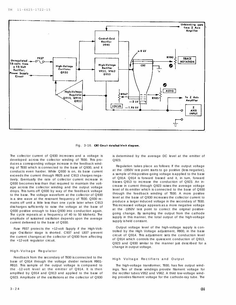
TM 11-6625-1722-15
Fig. 3-16. CRT Circuit detailed block diagram.
The collector current of Q930 increoses and a voltage is is determined by the average DC level at the emitter ofdeveloped across the collector winding of T930. This pro- Q923.duces a corresponding voltage increase in the feedback wind-ing of T930 which is connected to the base of Q930, and itconducts even harder. While Q930 is on, its base currentexceeds the current through R925 and C913 charges nega-tively. Eventually the rate of collector current increase inQ930 becomes less than that required to maintain the volt-age across the collector winding and the output voltagedrops. This turns off Q930 by way of the feedback voltageto the base. The voltage waveform at the collector of Q930is a sine wave at the resonant frequency of T930. Q930 re-mains off until a little less than one cycle later when C913discharges sufficiently to raise the voltage at the base ofQ930 positive enough to bias Q930 into conduction again.The cycle repeats at a frequency of 40 to 50 kilohertz. Theamplitude of sustained oscillation depends upon the averagecurrent delivered to the base of Q930.
Fuse F937 protects the +12-volt Supply if the High-Volt-age Oscillator stage is shorted. C937 and L937 preventthe current changes at the collector of Q930 from affectingthe +12-volt regulator circuit.
H i g h - V o l t a g e R e g u l a t o r
Feedback from the secondary of T930 is connected to thebase of Q914 through the voltage divider network R901-R910. This sample of the output voltage is compared tothe -12-volt level at the emitter of Q914. It is thenamplified by Q914 and Q913 and applied to the base ofQ923. Amplitude of the oscillations at the collector of Q930
Regulation takes place as follows: If the output voltageat the -1950V test point starts to go positive (less negative),a sample of this positive-going voltage is applied to the baseof Q914. Q914 is forward biased and it, in turn, forwardbiases Q913 to increase the conduction of Q923. An in-crease in current through Q923 raises the average voltagelevel of its emitter which is connected to the base of Q930through the feedback winding of T930. A more positivelevel at the base of Q930 increases the collector current toproduce a larger induced voltage in the secondary of T930.This increased voltage appears as a more negative voltageat the -1950V test point to correct the original positive-going change. By sampling the output from the cathodesupply in this manner, the total output of the high-voltagesupply is held constant.
Output voltage level of the high-voltage supply is con-trolled by the High Voltage adjustment, R900, in the basecircuit of Q914. This adjustment sets the conduction levelof Q914 which controls the quiescent conduction of Q913,Q923 and Q930 similar to the manner just described for achange in output voltage.
H i g h V o l t a g e R e c t i f i e r s a n d O u t p u t
The high-voltage transformer, T930, has five output wind-ings. Two of these windings provide filament voltage forthe rectifier tubes V952 and V962. A third low-voltage wind-ing provides filament voltage for the cathode-ray tube. The
3 - 2 4

TM 11-6625-1722-15
filament voltage can be supplied from the high-voltagesupply since the cathode-ray tube has a very low filamentcurrent drain. Two high-voltage windings provide the nega-tive and positive accelerating voltage and the CRT grid biasvoltage. All of these outputs are regulated by the High-Voltage Regulator stage in the primary of T930 to hold theoutput voltage constant.
Positive accelerating potential is supplied by voltage doub-ler V952 and V962. Regulated voltage output is about +8kilovolts. Ground return for this supply is through the resis-tive helix inside the cathode-ray tube to pin 7 and then toground through R972.
The negative accelerating potential for the CRT cathodeis supplied by the half-wave rectifier D952. Voltage outputis about -1.95 kilovolts. A sample of this output voltage isconnected to the High-Voltage Regulator stage to provide aregulated high-voltage output.
The half-wave rectifier D940 provides a negative voltagefor the control grid of the CRT. Output level is adjustableby R940, CRT Grid Bias adjustment. The neon bulbs B973,B974 and B975 provide protection if the voltage differencebetween the control grid and cathode exceeds about 165volts. The unblanking gate from the Z Axis Amplifier isapplied to the positive side of this circuit to produce achange in output voltage to control CRT intensity, unblank-ing, dual-trace blanking and intensity modulation.
C R T C o n t r o l C i r c u i t s
Focus of the CRT display is controlled by the FOCUS con-trol, R967. Divider R963-R968 is connected between the CRTcathode supply and ground. The voltage applied to thefocus grid is more positive (closer to ground level) than thevoltage on either the control grid or the CRT cathode. TheASTIG adjustment, R985, which is used in conjunction withthe FOCUS control to provide a well-defined display, variesthe positive level on the astigmatism grid. The +90-voltsource for this control is provided by zener diode D1043 inthe Z Axis Amplifier circuit.
Geometry adjustment, R982, varies the positive level onthe horizontal deflection plate shields to control the overallgeometry of the display. Two adjustments control the tracealignment by varying the magnetic fields around the CRT.The Y Axis Align adjustment, R989, controls the currentthrough L989 which affects the CRT beam after vertical de-flection but before horizontal deflection. The TRACE ROTA-TION adjustment, R980, controls the current through L980and affects both vertical and horizontal rotation of the beam.
E x t e r n a l Z A x i s I n p u t
A signal applied to the Z AXIS INPUT connector (see ZAxis Amplifier schematic) is applied to the CRT cathodethrough C979-C976-R976. DC and low frequency Z-axis sig-nals are blocked from the CRT circuit by C979. They areconnected to the Z Axis Amplifier circuit to produce an in-crease or decrease in intensity, depending upon polarity.C976 and C979 couple high-frequency signals directly to theCRT cathode to produce the same resultant display as theZ Axis Amplifier circuit produces for low-frequency signals.
This configuration operates as a crossover network to providenearly constant intensity modulation from DC to 50 mega-hertz.
L O W - V O L T A G E P O W E R S U P P L Y
G e n e r a l
The low-voltage Power Supply circuit provides the operat-ing power for this instrument from three regulated suppliesand one unregulated supply. Electronic regulation11 is usedto provide stable, low-ripple output voltages. Each regulatedsupply contains a short-protection circuit to prevent instru-ment damage if a supply is inadvertently shorted to ground.The Power Input stage includes the Line Voltage Selectorassembly. This assembly allows selection of the nominaloperating voltage and regulating rcrnge for the instrument.Fig. 3-17 shows a detailed block diagram of the PowerSupply circuit. A schematic of this circuit is shown on dia-gram 17 at the rear of this manual.
P o w e r I n p u t
Power is applied to the primary of transformer T1101through the 115-volt line fuse F1101, POWER switch SW1101,thermal cutout TK1101, Voltage Selector switch SW1102 andRange Selector switch SW1103. The Voltage Selector switchSW1102 connects the split primaries of T1101 in parallel for115-volt nominal operation, or in series for 230-volt nominaloperation. A second line fuse, F1102, is connected into thecircuit when the Voltage Selector switch is set to the 230 Vposition to provide the correct protection for 230-volt opera-tion (F1102 current rating is one-half of F1101). The fan isconnected across one half of the split primary winding so italways has about 115 volts applied to it.
The Range Selector switch, SW1103, allows the instrumentto regulate correctly on higher or lower than normal linevoltages. Each half of the primary has taps above andbelow the 115-volt (230) nominal point. As the Range Selec-tor switch, SW1103, is switched from LO to M to Hl, moreturns are effectively added to the primary winding and theturns ratio is decreased. This provides a fairly constant volt-age in the secondary of T1101 even through the primaryvoltage has increased.
Thermal cutout TK1101 provides thermal protection for thisinstrument. If the internal temperature of the instrument ex-ceeds a safe operating level, TK1101 opens to interrupt theapplied power. When the temperature returns to a safelevel, TK1101 automatically closes to reapply the power.
-12-volt Supply
The -12-Volt Supply provides the reference voltage forthe remaining supplies. The output from the secondary ofT1101 is rectified by bridge rectifier D112A-D. This voltage isfiltered by C1112 and then applied to the -12-Volt SeriesRegulator stage to provide a stable output voltage. TheSeries Regulator can be compared to a variable resistancewhich is changed to control the output current. The currentthrough the Series Regulator stage is controlled by the ErrorAmplifier to provide the correct regulated output voltage.
“~utler, pp. 559-625.
3 - 2 5

3-26
TM 11-6625-1722-15
F i g . 3 - 1 7 . Power Supply detailed block diagram.

TM 11-6625-1722-15
The Error Amplifier is connected as a comparator. Refer-ence voltage for the comparator is provided by zener diodeD1114 which sets the base of Q1114 at about –9 volts. Thebase level of Q1124 is determined by voltage divider R1121-R1122-R1123 between the output of this supply and ground.R1122 is adjustable to set the output voltage of this supplyto -12 volts. R1119 is the emitter resistor for both com-parator transistors and the current through it divides be-tween Q1114 and Q1124. The output current of the ErrorAmplifier stage controls the conduction of the Series Regula-tor stage (through Q1133). This output current changes toprovide a canstant, low-ripple –12-volt output level. Thisoccurs as follows: The -12-volt regulatar maintains equalvoltage at the bases of the Error Amplifier transistors Q1114and Q1124. If the -12 Volts adjustment R1122, is turnedclockwise, the current through Q1124 increases (Q1124 basetends to go more positive than the base of Q1114) and thecurrent through Q1114 decreases. Decreased current throughQ1114 produces less voltage drop across R1117 and the baseof Q1133 goes positive. The emitter of Q1133 pulls the baseof Q1137 positive to increase the current through the load,thereby increasing the output voltage of the supply. Thisplaces more voltage across divider R1121-R1122-R1123 andthe divider action returns the base of Q1124 to about -9volts. A similar, but opposite, action takes place when R1122is turned counterclockwise so the base of Q1124 is morenegative than the base of Q1114. The -12 Volts adjustmentR1122, is set to provide a -12-volt level at the output ofthis supply.
The output voltage is regulated to provide a constant volt-age to the load by feeding a sample of the output back tothe Series Regulator, Q1137. For example, assume that theoutput voltage increases (more negative) because of a changein load or an increase in line voltage. This negative-goinglevel at the output is applied across the voltage dividerR1121-R1122-R1123 and the base of Q1124 goes negativealso. This reduces the current flow through Q1124 whichallows Q1114 to conduct more and its collector goes nega-tive. When the collector of Q1114 goes negative, the biason Q1133 is reduced, resulting in reduced current throughthe Series Regulator, Q1137. Reduced current through Q1137also means that there is less current through the load andthe output voltage decreases (less negative). In a similarmanner the Series Regulator and Error Amplifier stages com-pensate for output changes due to ripple.
The Short-Protection Amplifier stage, Q1129, protects the-12-Volt Supply if the output is shorted. For normal opera-tion, the emitter-base voltage of Q1129 is not enough tobias it on. However, when the output is shorted, high currentis demanded from the -12-Volt Supply, and this currentflows through R1129. The voltage drop across R1129 becomessufficient to forward bias Q1129 and its collector currentproduces an increased voltage drop across R1117. Theincreased voltage drop across R1117 reduces the current flowof both Q1133 and Q1137 to limit the output current.
+12-Volt Supply
Rectified voltage for operation of the +12-Volt Supply isprovided by D1142 A-D. This voltage is filtered by C1142and connected to the +12-Volt Supply Series Regulator andto the High-Voltage Oscillator stage in the CRT Circuit. Ref-erence voltage for this supply is provided by voltage divider
R1151-R1152-R1153 between the regulated -12 volts andthe output of this supply. The -12 volts is held stable by the–12-Volt Supply as discussed previously. If the +12-voltoutput changes, a sample of this change appears at thebase of Q1154 as an error signal. Regulation of the outputvoltage is controlled by the +12-Volt Series Regulator stage,Q1167, in a similar manner to that described for the –12-Volt Supply. The +12 Volts adjustment, R1152, sets theoutput level to +12 volts. D1152 provides thermal com-pensation for the Error Amplifier. C1164 improves responseof the regulator circuit to AC changes at the output.
Shorting protection is provided by Q1159 and R1159. Ifthe output of this supply is shorted, Q1159 is biased on tolimit the conduction of the Series Regulator in the same man-ner as described for the -12-Volt Short-Protection Amplifier.D1164 protects Q1154 when the output of this supply isshorted.
+75-Volt Supply
D1172 A-D provides the rectified voltage for the +75-Volt Supply. C1172 filters the rectified voltage which is con-nected to the +75-Volt Series Regulator. Reference voltagefor this supply is provided by voltage-divider R1181-R1182-R1183 between the regulated -12 volts and the output ofthis supply. Since the -12 volts is held stable by the -12-Volt Regulator circuit, any change at the base of Error Ampli-fier Q1184 is due to change at the output of the +75-Volt Supply. Regulation of the output voltage is controlledby Error Amplifier Q1184-Q1193 and Series Regulator,Q1197, in a manner similar to that described for the +12-Volt Supply. The +75 Volts adjustment R1182, sets thequiescent conduction level of the Error Amplifier stage to pro-vide an output level of +75 volts. The output of the +150-Volt Supply (unregulated) is connected to the Error Ampli-fier to provide the required collector supply for stable opera-tion. Zener diode D1209 establishes a volage at its cathodeof about +108 volts. Then, R1186, zener diode D1185 andR1185 drop this voltage to the correct level for the operationof Q1184. D1182 provides thermal compensation for theError Amplifier.
Q1189 provides current limiting for this supply throughD1188. Quiescently, Q1189 is off and under normal operat-ing conditions, D1189 is conducting and D1188 is reversebiased. However, when the output is shorted, the increasedcurrent flow thraugh R1187 biases Q1189 on and its collectorgoes negative. This forward biases D1188 and reversebiases D1189. Now Q1189 limits the collector current ofQ1197 through Q1193. F1172 also provides overload pro-tection. D1198 protects the +75-volt supply from damageif it is shorted to the -12-volt output.
+150-Volt Unregulated Supply
Rectifiers D1202 and D1212 provide the unregulated out-put for the +150-Volt Supply. The output of the +75-VoltSupply is connected to the negative side of the +150-VoltSupply to elevate the output level to +150 volts. DiodesD1202 and D1212 are connected as a full-wave center-tappedrectifier and the output is filtered by C1202-C1204-R1204 tohold the output level at about +150 volts. Fuse F1204 pro-tects this supply if the output is shorted.
3 - 2 7

TM 1 1 - 6 6 2 5 - 1 7 2 2 - 1 5
6 . 3 - V o l t R M S A C S o u r c e
The 6.3-volt RMS secondary winding of T1101 providespower for the POWER ON light, B1107, and the scale illu-mination lights, B1108 and B1109. The current through thescale illumination lights is controlled by the SCALE ILLUMcontrol, R1108, to change the illumination of the graticuleline voltage to the A and B Trigger Generatar circuits forline voltage to the A and B Trigger Generaar circuits forinternal triggering at the line frequency. C1105 reducesnoise on the line frequency signal.
V O L T A G E D I S T R I B U T I O N
Diagram 17 also shows the distribution of the output volt-ages from the Power Supply circuit to the circuit boards inthis instrument. The decoupling networks which provide de-coupled operating voltages are shown on this Diagram andare not repeated on the individual circuit diagrams.
C A L I B R A T O R
Genera l
The Calibrator circuit produces a square-wave output withaccurate amplitude and frequency. This output is availableas a square-wave voltage at the 1 kHz CAL connector oras a square-wave current through the side-panel PROBELOOP. Fig. 3-18 shows a detailed block diagram of the Cali-bratar circuit. A schematic of this circuit is shown on dia-gram 18 at the rear of this manual.
Osci l lator
Q1255 and its associated circuitry comprise a tuned-col-lector oscillator.12 Frequency of oscillation is determined bythe LC circuit comprised of the primary of variable trans-former T1255 in parallel with C1255. The accuracy and sta-
bility required to provide an accurate time and frequencyreference is obtained by using a capacitor and transformerwhich have equal but opposite temperature coefficients.
The oscillations of the LC circuit, T1255-C1255, are sus-tained by the feedback winding of T1255 connected to thebase of Q1255. C1266 connects a sample of the output ofthe LC circuit to the base of Q1265. The regenerative feed-back from the emitter of Q1265 to the emitter of Q1255 pro-duces fast changeover between Q1255 and Q1265 to pro-vide a fast risetime on the output square wave. Frequencyof the output square wave can be adjusted by varying thecoupling to the feedback winding of T1255. The square-wave signal at the collector of Q1265 is connected to theOutput Amplifier.
O u t p u t A m p l i f i e r
The output signal from the oscillator stage saturates Q1274to produce the accurate square wave at the output. Whenthe base of Q1274 goes positive, Q1274 is cut off and theoutput signal drops negative to ground. When its basegoes negative, Q1274 is driven into saturation and the out-put signal rises positive to about +12 volts. The output ofthe +12-Volt Supply is adjusted for an accurate one-voltoutput signal at the 1 kHz CAL connector when the Cali-brator switch is set to 1 V.
O u t p u t D i v i d e r
The Output Divider, R1275-R1276-R1277, provides twooutput voltages from the Calibrator circuit. In the 1 V CALl-BRATOR switch position, voltage is obtained from the cal-Iector of Q1274 through R1274. In the .1 V CALIBRATORswitch position, the output is obtained at the junction ofvoltage divider R1275 and R1276-R1277 to provide one-tenthof the previous output voltage.
Collector current of Q1274 flows through the PROBELOOP on the side panel. Output current is a five-millampere
“Lloyd P. Hunterr pp. 14-3—1 4.7. square wave.
3 - 2 8
F i g . 3 - 1 8 . Calibrator detailed block diagram.

TM 11-6625-1722-15
S E C T I O N 4
M A I N T E N A N C E
In t roduct ion
This section of the manual contains maintenance informa-tion for use in preventive maintenance, corrective mainten-ance or troubleshooting of the Type 453.
C o v e r R e m o v a l
The top and bottom covers of the instrument are held inplace by thumb screws located on each side of the instru-ment. To remove the covers, loosen the thumb screws andslide the covers off the instrument. The covers protect theinstrument from dust in the interior. The covers also directthe flow of cooling air and reduce the EMI radiation fromthe instrument.
P R E V E N T I V E M A I N T E N A N C E
G e n e r a l
Preventive maintenance consists of cleaning, visual inspec-on, lubrication, etc. Preventive maintenance performed on
a regulor basis may prevent instrument breakdown and willimprove the reliability of this instrument. The severity of theenvironment to which the Typethe frequency of maintenance.
453 is subjected determines
Cleaning
General. The Type 453 should be cleaned as aften osoperating conditions require. Accumulation of dirt in theinstrument can cause overheating and component breakdown.Dirt on components acts as an insulating blanket and preventsefficient heat dissipation. It also provides an electricalconduction path.
CAUTION
Avoid the use of chemical cleaning agents whichmight damage the plastics used in this instrument.Avoid chemicals which contain benzene, toluene,xylene, acetone or similar solvents.
The top and bottom covers provide protection against dustn the interior of the instrument. Operation without the
covers in place necessitates more frequent cleaning. Thefront cover provides dust protection for the front panel andthe CRT face. The front cover should be installed for stor-age or transportation. The plastic cover supplied with theType 453 provides protection for the outside of the instru-ment during transportation or storage. The pocket on theside also provides a convenient place to carry this instruc-tion manual.
Air Filter. The air filter should be visually checked everyfew weeks and cleaned or replaced if dirty. More frequentinspections are required under severe operating conditions.The following procedure is suggested for cleaning the filter.
1. Remove the filter by pulling it out of the retainingframe on the rear panel. Be careful not to drop any of theaccumulated dirt into the instrument.
2. Flush the loose dirt from the filter with a stream of hotwater.
3. Place the filter in a solution of mild detergent and hotwater and let it soak for several minutes.
4.
5.
6.
7.
8.
Squeeze the filter to wash out any dirt which remains.
Rinse the filter in clear water and allow it to dry.
Coat the dry filter with an air-filter adhesive,:
Let the adhesive dry thoroughly.
Re-install the filter in the retaining frame.
Exterior. Loose dust accumulated on the outside of theType 453 can be removed with a soft cloth or small paintbrush. The paint brush is particularly useful for dislodgingdirt on and around the front-panel controls. Dirt which re-mains can be removed with a soft cloth dampened in a milddetergent and water solution. Abrasive cleaners should notbe used.
CRT. Clean the plastic light filter, faceplate protector andthe CRT face with a soft, lint-free cloth dampened with de-natured alcohol. The CRT mesh fiiter can be cieaned in thefollowing manner.
1. Hold the filter in a vertical position and brush lightlywith a soft #7 water-color brush to remove light coatings ofdust or lint.
2. Greasy residues or dried-on dirt can be removed witha solution of warm water and a neutral-pH liquid deter-gent. Use the brush to lightly scrub the filter.
3. Rinse the filter thoroughly in clean water and allow toair dry.
4. If any lint or dirt remains, use clean low-pressure airto remove. Do not use tweezers or other hard cleaning toolson the filter, as the special finish may be damaged.
5. When not in use, store the mesh fiiter in a lint-free,dust-proof container such as a plastic bag.
4 - 1

TM 11-6625-1722-15
Interior. Dust in the interior of the instrument should beremoved occasionally due to its electrical conductivity underhigh-humidity conditions. The best way to clean the interiorit to blow off the accumulated dust with dry, low-velocityair. Remove any dirt which remains with a soft paint brushor a cloth dompened with a mild detergent and water solu-tion. A cotton-tipped applicator is useful for cleaning innarrow spaces or for cleaning ceramic terminal strips andcircuit boards.
The high-voltage circuits, particularly parts located inthe high-voltage compartment and the area surrounding thepost-deflection anode connector, should receive specialattention. Excessive dirt in these areas may cause high-voltage arcing and result in improper instrument operation.
Lubrication
General. The reliability of potentiometers, rotary switchesand other moving parts can be maintained if they are keptproperly lubricated. Use a cleaning-type lubricant (e.g.,Tektronix Part No. 006-0218-00) on switch contacts. Lubri-cate switch detents with a heavier grease (e.g., TektronixPart No. 006-0219-00). Potentiometers which are not per-manently sealed should be lubricated with a lubricant whichdoes not affect electrical characteristics (e.g., Tektronix PartNo. 006-0220-00). The pot lubricant can also be used onshaft bushings. Do not over-lubricate. A lubrication kit con-taining the necessary lubricants and instructions is availablefrom Tektronix, Inc. Order Tektronix Part No. 003-0342-00.
Fan. The fan-motor bearings are sealed and do not re-quire lubrication.
Visual Inspection
The Type 453 should be inspected ossasionally for suchdefects as broken connections, broken or damaged ceramicstrips, improperly seated transistors, damaged circuit boardsand heat-damaged parts.
The corrective precedure for most visible defects is obvi-ous; however, particular care must be taken if heat-damagedcomponents are found. Overheating usually indicates othertrouble in the instrument; therefore, it is important that thecause of over-heating be corrected to prevent recurrence ofthe damage.
Transistor Checks
Periodic checks of the transistors in the Type 453 are notrecommended. The best check of transistor performance isits actual operation in the instrument. More details on check-ing transistor operation is given under Troubleshooting.
Recalibration
To assure accurate measurements, check the calibration ofthis instrument after each 1000 hours of operation or everysix months if used infrequently. In addition, replacement ofcomponents may necessitate recalibration of the affectedcircuits. Complete calibration instructions are given in theCalibration section.
The calibration procedure can also be helpful in localiz-ing cerain troubles in the instrument. In some cases, minor
troubles may be revealed and/or corrected by recalibra-tion.
TROUBLESHOOTING
Introduction
The following information is provided to facilitate trouble-shooting of the Type 453. Information contained in othersections of this manual should be used along with the fol-lowing information to aid in locating the defective compon-ent. An understanding of the circuit operation is very help-ful in locating troubles. See the Circuit Description sectionfor complete information.
Troubleshooting Aids
Diagrams. Circuit diagrams are given on foldout pagesin Section 9. The component number and electrical value ofeach component in this instrument are shown on the dia-grams. Each main circuit is assigned a series of componentnumbers. Table 4-1 lists the main circuits in the Type 453 andthe series of component numbers assigned to each. Import-ant voltages and waveforms are also shown on the diagrams.The portions of the circuit mounted on circuit boards areenclosed with a blue line.
TABLE 4-1
Switch Wafer Identification. Switch wafers shown onthe diagrams are coded to indicate the position of the waferin the complete switch assembly. The numbered portion ofthe code refers to the wafer number counting from the front,or mounting end of the switch, toward the rear. The lettersF and R indicate whether the front or rear of the wafer per-forms the particular switching function. For example, a waferdesignated 2R indicates that the rear of the second waferfrom the front is used for this particular switching function.
Circuit Boards. Fig. 4-6 through 4-14 show the circuitboards used in the Type 453. Fig. 4-5 shows the locationof each board within the instrument. Each electrical com-ponent on the boards is identified by its circuit number.
4 -2

TM 11-6625-1722-15
The circuit boards are also outlined on the diagrams with ablue line. These pictures, used along with the diagrams, aidin locating the components mounted on the circuit boards.
Wiring Color-Code. All insulated wire and cable usedin the Type 453 is color-coded to facilitate circuit tracing.Signal carrying leads are identified with one or two coloredstripes. Voltage supply leads are identified with three stripesto indicate the approximate voltage using the EIA resistorcolor code. A white background color indicates a positivevoltage and a tan background indicates a negative voltage.The widest color stripe identifies the first color of the code.Table 4-2 gives the wiring color-code for the power-supplyvoltages used in the Type 453.
TABLE 4-2
Power Supply Wiring Color Code
Resistor Color-Code. In addition to the brown com-position resistors, some metal-film resistors and some wire-wound resistors are used in the Type 453. The resistancevalues of wire-wound resistors are printed on the body ofthe component. The resistance values of composition resis-tors and metal-film resistors are color-coded on the compon-ents with EIA color-code (some metal-film resistors may havethe value printed on the body). The color-code is read start-ing with the stripe nearest the end of the resistor. Com-position resistors have four stripes which consist of two signi-ficant figures, a multiplier and a tolerance value (see Fig.4-1). Metal-film resistors have five stripes consisting of threesignificant figures, a multiplier and a tolerance value.
Capacitor Marking. The capacitance values of commondisc capacitors and small elecrolytics are marked in micro-farads on the side of the component body. The white ceramiccapacitors used in the Type 453 are color coded in picofaradsusing modified EIA code (see Fig. 4-1).
Diode Color Code. The cathode end of each glass-en-cased diode is indicated by a stripe, a series of stripes or adot. For most silicon or germanium diodes with a series ofstripes, the color-code also indicates the type of diode andidentifies the Tektronix Part Number using the resistor color-code system (e.g., a diode color-coded blue-brown-gray-green indicates diode type 6185 with Tektronix Part Number
F i g . 4 - 1 . Celor cad. for resistars and ceramic capacitors.
4 - 3

TM 11-6625-1722-15
F i g . 4 - 2 . Electrode configuration for semiconductors in this instrument.
152-0185-00). The cathode and anode end of metal-encased NOTEdiodes can be identified by the diode symbol marked on thebody. A 20,000 ohms/volt VOM can be used to check
Transistor Lead Configuration. Fig. 4-2 shows the leadthe voltages in this instrument if allowances are
configurations of the transistors used in this instrument. Thismade for the circuit loading of the VOM at high-impedance points.
view is as seen from the bottom of the transistors.
T r o u b l e s h o o t i n g E q u i p m e n t
The following equipment is useful for troubleshooting the
Type 453.
1. Transistor Tester
Description: Tektronix Type 575 Transistor-Curve Traceror equivalent.
Purpose: To test the semiconductors used in this instrument.
2. Multimeter
Description: VTVM, 10 megohm input impedance and 0 to500 volts range; ohmmeter, 0 to 50 megohms. Accuracy, with-in 3%. Test prods must be insulated to prevent accidentalshorting.
Purpose: To check voltages and for general troubleshoot-ing in this instrument.
3. Test Oscilloscope
Description: DC to 20 MHz frequency response. 5 milli-volts to 10 volts/division deflection factor. Use a 10Xprobe.
Purpose: To check waveforms in this instrument.
T roubleshoot ing Techniques
This troubleshooting procedure is arranged in an orderwhich checks the simple possibilities before proceeding withextensive troubleshooting. The first few checks assure properconnection, operation and calibration. If the trouble is notlocated by these checks, the remaining steps aid in locatingthe defective component. When the defective component islocated, it should be replaced following the replacement pro-cedures given under Corrective Maintenance.
4 - 4

TM 1 1 - 6 6 2 5 - 1 7 2 2 - 1 5
1. Check Control Settings. Incorrect control settings can the page until a step is found which is not correct. Furtherindicate a trouble that does not exist. If there is any question checks and/or the circuit in which the trouble is prabablyabout the correct functian or operation of any control, see located are listed to the right of this step.the Operating Instructions section of this manual.
After the defective circuit-has been located, proceed with
2. Check Associated Equipment. Before proceeding with steps 6 through 8 to locate the defective component(s).
troubleshooting of the Type 453, check that the equipmentused with this instrument is operating correctly. Check that 6. Check Circuit Board Interconnections. After the
the signal is properly connected and that the interconnecting trouble has been isolated to a particular circuit, check the
cables are not defective. Also, check the power source. pin connectors on the circuit board for correct connection.Figs. 4-8 through 4-16 show the correct connections for each
3. Visual Check. Visually check the portion of the instru-ment in which the trouble is located. Many troubles can belocated by visual indications such as unsoldered connections,broken wires, damaged circuit boards, damaged components,etc.
4. Check Instrument Calibration. Check the calibrationof this instrument, or the affected circuit if the trouble existsin one circuit. The apparent trouble may only be a result ofmisadjustment or may be corrected by calibration. Completecalibration instructions are given in the Calibration sectionof this manual.
5. Isolate Trouble to a Circuit. To isolate trouble to acircuit, note the trouble symptom. The sympton often identi-fies the circuit in which the trouble is located. For example,poor focus indicates that the CRT (includes high voltage)circuit is probably at fault. When trouble symptoms appearin more than one circuit, check affected circuits by takingvoltage and waveform readings. Also check for the correctoutput signals at the side-panel output connectors with atest oscilloscope. If the signal is correct, the circuit is work-ing correctly up to that point. For example, correct ampli-tude and time of the A Gate out waveform indicates thatthe A Trigger Generatar and A Sweep Gate circuits areoperating correctly.
Incorrect operation of all circuits often indicates trouble inthe power supply. Check first for correct voltage of the indi-vidual supplies. However, a defective component elsewherein the instrument can appear as a power-supply troubleand may also affect the operation of other circuits. Table4-3 lists the tolerances of the power supplies in this instru-ment. [f a power-supply voltage is within the listed tolerance,the supply can be assumed to be working correctly. If out-side the tolerance, the supply may be misadjusted or operat-ing incorrectly. Use the procedure given in the Calibrationsection to adjust the power supplies.
TABLE 4-3
Power Supply Tolerance
lAd@ed for eorreet output from the Calibrator circuit; see Calibra-tion procedure.
Fig. 4-3 provides a guide to aid in locating a defectivecircuit. This chart may not include checks for all possibledefects; use steps 6-8 in such cases. Start from the topof the chart and perform the given checks on the left side of
board.
The pin connectors used in this instrument also provide aconvenient means of circuit isolation. Far example, a shortin a power supply can be isolated to the power supply itselfby disconnecting the pin connectors for that voltage at theremaining boards.
7. Check Voltage and Waveforms. Often the defectivecomponent can be located by checking for the correct volt-age or waveform in the circuit. Typical voltages and wave-forms are given on the diagrams.
NOTE
Voltages and wavefarms given on the diagramsare not absolute and may vary slightly betweeninstruments. To obtain operating conditions similarto those used to take these readings, see the firstdiagram page.
8. Check Individual Components. The following proce-dures describe methods of checking individual componentsin the Type 453. Components which are soldered in placeare best checked by disconnecting one end. This isolates themeasurement from the effects of surrounding circuitry.
A. TRANSISTORS. The best check of transistor operationis actual performance under aperating conditions. If atransistor is suspected of being defective, it can best bechecked by substituting a new component or one whichhas been checked previously. However, be sure that circuitconditions are not such that a replacement transistor mightalso be damaged. If substitute transistors are not available,use a dynamic tester (such as Tektronix Type 575). Static-type testers are not recommended, since they do not checkoperation under simulated operating conditions.
B. DIODES. A diode can be checked for an open orshorted condition by measuring the resistance betweenterminals. With an ohmmeter scale having an internalsource of between 800 millivolts and 3 volts, the resistanceshould be very high in one direction and very low when theleads are reversed.
CAUTION
Do not use an ohmmeter scale that has a highinternal current. High currents may damage thediode. Do not measure tunnel diodes with an ohm-meter; use a dynamic tester (such as a TektronixType 575 Transistor-Curve Tracer).
C. RESISTORS. Check the resistors with an ohmmeter.Check the Electrical Parts List for the tolerance of the resis-tors used in this instrument. Resistors normally do not needto be replaced unless the measured value varies widely fromthe specified value.
4 - 5

TM
11-6625-1722-15
4-
6

Fig. 4-3.
TM
11-6625-1722-154
-7

TM 1 1 - 6 6 2 5 - 1 7 2 2 - 1 5
D. INDUCTORS. Check forcontinuity with an ohmmeter.
open inductors by checkingShorted or partially shorted
inductors can usually be found by checking the waveformresponse when high-frequency signals are passed throughthe circuit. Partial shorting often reduces high-frequencyresponse (roll-off).
E. CAPACITORS. A leaky or shorted capacitor can best bedetected by checking resistance with an ohmmeter on thehighest scale. Do not exceed the voltage rating of thecapacitor. The resistance reading should be high afterinitial charge of the capacitor. An open capacitor can bestbe detected with a capacitance meter or by checking whetherthe capacitor passes AC signals.
9. Repair and Readjust the Circuit. If any defectiveparts are Iocated, follow the replacement procedures givenin this section. Be sure to check the performance of any cir-cuit that has been repaired or that has had any electricalcomponents replaced.
C O R R E C T I V E M A I N T E N A N C E
G e n e r a l
Corrective maintenance consists of component replacementand instrument repair. Special techniques required to replacecomponents in this instrument are given here.
Solder ing Techniques
WARNING
Disconnect the instrument from the power sourcebefore soldering.
Circuit Boards. Use ordinary 60/40 solder and a 35- to40-watt pencil type soldering iron on the circuit boards.The tip of the iron should be clean and properly tinned forbest heat transfer to the solder joint. A higher wattagesoldering iron may separate the wiring from the basematerial.
The following technique should be used to replace acomponent on a circuit board. Most components can bereplaced without removing the boards from the instrument.
1. Grip the component lead with long-nose pliers. Touchthe soldering iron to the lead at the solder connection. Donot lay the iron directly on the board.
2. When the solder begins to melt, pull the lead outgently. This should leave a clean hole in the board. If not,the hole can be cleaned by reheating the solder and placinga sharp object such as a toothpick into the hole to clean itout. A vacuum-type resoldering tool can also be used forthis purpose.
3. Bend the leads of the new component to fit the holesin the board. If the component is replaced while the boardis mounted in the instrument, cut the leads so they will justprotrude through the board. Insert the leads into the holesin the board so the component is firmly seated against theboard (or as positioned originally). If it does not seat prop-erly, heat the solder and gently press the component intoplace.
4. Touch the iron to the connection and apply a smallamount of solder to make a firm solder joint; do not applytoo much solder. To protect heat-sensitive components, holdthe lead between the component body and the solder jointwith a pair of long nose pliers or other heat sink.
5. Clip the excess lead that protrudes through the board.
6. Clean the area around the solder connection with aflux-remover solvent. Be careful not to remove informationprinted on the board.
Ceramic Terminal Strips. Solder used on the ceramicterminal strips should contain about 3% silver. Use a 40-to 75-watt soldering iron with atip. Ordinary solder should not be usedo n the ceramic terminal strips. If ordinarysolder is used repeatedly or if excessive heat is applied,the solder-to-ceramic bond may be broken.
A sample roll of solder containing about 3% silver ismounted on the rear subpanel of this instrument. Additionalsolder of the same type should be available locally, or it
c a n b e p r o c u r e d u n d e r F S N 3 4 3 9 - 9 1 2 - 8 6 9 8 .
4 - 8
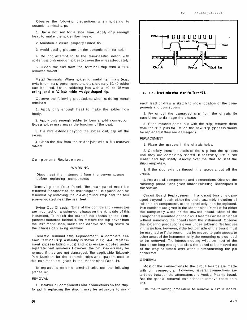
TM 11-6625-1722-15
Observe the following precautions when soldering toceramic terminal strips.
1. Use a hot iron for a shorT time. Apply only enoughheat to make the solder flow freely.
2. Maintain a clean, properly tinned tip.
3. Avoid putting pressure on the ceramic terminal strip.
4. Do not attempt to fill the terminal-strip notch withsolder; use only enough solder to cover the wires adequately.
5. Clean the flux from the terminal strip with a flux-remover solvent.
Metal Terminals. When soldering metal terminals (e.g.,switch terminals, potentiometers, etc), ordinary 60/40 soldercan be used. Use a soldering iron with a 40- to 75-watt
Observe the following precautions when soldering metalterminals:
1. Apply only enough heat to make the solder flowfreely.
2. Apply only enough solder to form a solid connection.Excess solder may impair the function of the part.
3. If a wire extends beyond the solder joint, clip off theexcess.
4. Clean thesolvent.
C o m p o n e n t
flux from the solder joint with a flux-remover
Replacement
WARNING
Disconnect the instrument from the power sourcebefore replacing components.
Removing the Rear Panel. The rear panel must beremoved for access to the rear subpanel. This panel can beremoved by removing the Z Axis ground strap and the fourscrews located near the rear feet.
Swing-Out Chassis. Some of the controls and connectorsare mounted on a swing-out chassis on the right side of thisinstrument. To reach the rear of this chassis or the com-ponents mounted behind it, first remove the top cover fromthe instrument. Then, loosen the captive securing screw sothe chassis can swing outward.
Ceramic Terminal Strip Replacement. A complete cer-amic terminal strip assembly is shown in Fig. 4-4. Replace-ment strips (including studs) and spacers are supplied underseparate part numbers. However, the old spacers may bere-used if they are not damaged. The applicable Tektronix
Part Numbers for the ceramic strips and spacers used in this instrument are given in the Mechanical Parts List.
To replace a ceramic terminal strip, use the followingpracedure:
REMOVAL:
1. Unsolder all components and connections on the strip.To aid ih replacing the strip, it may be advisable to mark
F i g . 4 - 4 . Troubleshooting chart for Type 453.
each lead or draw a sketch to show location of the com-ponents and connections.
2. Pry or pull the damaged strip from the chassis. Becareful not to damage the chassis.
3. If the spacers come out with the strip, remove themfrom the stud pins for use on the new strip (spacers shouldbe replaced if they are damaged).
REPLACEMENT:
1. Place the spacers in the chassis holes.
2. Carefully press the studs of the strip into the spacersuntil they are completely seated. If necessary, use a softmallet and tap lightly, directly over the stud, to seat thestrip completely.
3. If the stud extends through the spacers, cut off theexcess.
4. Replace all components and connections. Observe thesoldering precautions given under Soldering Techniques inthis section.
Circuit Board Replacement. If a circuit board is dam-aged beyond repair, either the entire assembly including allsoldered-on components, or the board only, can be replaced.Part numbers are given in the Mechanical Parts List for eitherthe completely wired or the unwired board. Most of thecomponents mounted or, the circuit boards can be replacedwithout removing the boards from the instrument. Observethe soldering precautions given under Soldering Techniquesin this section. However, if the bottom side of the board mustbe reached or if the board must be moved to gain access toother areas of the instrument, only the mounting screws needto be removed. The interconnecting wires on most of theboards are long enough to allow the board to be moved outof the way or turned over without disconnecting the pinconnectors.
GENERAL:
Most of the connections to the circuit boards are madewith pin connectors. However, several connections aresoldered between the attenuators and Vertical Preamp board.See the special removal instructions to remove these as aunit.
Use the following procedure to remove a circuit board.
4 - 9

TM 11-6625-1722-15
1. Disconnect all pin connectors which come through holesin the board.
2. Remove aII screws holding the board to the chassis.
3. The board may now be lifted for maintenance or accessto areas beneath the board.
4. To completely remove the board, disconnect the remain-ing pin connectors.
5. Lift the circuit board out of the instrument. Do notforce or bend the board.
6. To replace the board, reverse the order of removal.Correct location of the pin connectors is shown in Fig. 4-8through 4-16. Replace the pin connectors (carefully so theymate correctly with the pins. If forced into place incorrectlypositioned, the pin connectors may be damaged.
VERTICAL PREAMP UNIT REMOVAL:
Use the following procedure to remove the Vertical Pre-amp board and the attenuators as a unit.
1. Remove the screw (mounted with a washer) which holdsthe MODE-TRIGGER switch (rear of board) to the chassis.The other screw may be left in place.
2. Remove the screw (with fiber washer) from the centerof the board.
3. Unsolder the connections on he MODE TRIGGER switchwhich do not go to the Vertical Prearnp board.
4. Disconnect all pin connectors which lead off of theVertical Preamp board.
5. Remove the attenuator shield and remove the nuts (four)located under this shield at each side of the INPUT con-nectors.
6. Remove the VARIABLE, CH 1 and CH 2 VOLTS/DIV,POSITION, Input Coupling, TRIGGER and MODE knobs.
7. Remove the securing nuts on the VOLTS/DIV switchesand the STEP ATTEN BAL controls.
8. Remove the three screws at the rear of the board.
9. Lift up on the rear of the assembly and slide it outof the instrument.
10. The board may now be removed from the VerticalPreamp unit as follows:
a. Disconnect all pin connectors remaining on theboard.
b. Unsolder all connections on the rear side of theboard which connect between the attenuators and theboard. Observe the soldering precautions given in thissection.
c. Remove the remaining screw whichi holds the MODE-TRIGGER switch to the board.
d. Remove the four screws holding the board to theattenuators.
11. To replace the unit, reverse the order of removal.Be sure the GAIN and INVERT extensions are positionedcorrectly in the corresponding front-panel holes.
Cathode-Ray Tube Replacement. Use care when han-dling a CRT. Protective clothing and safety glasses should
be worn. Avoid striking it on any object which might causeit to crock or implode. When storing a CRT, place it facedown On a smooth surface with a protective cover or softmat under the faceplate to protect it from scratches.
The CRT shield should also be handled carefully. Thisshield protects the CRT display from distortion due to mag-netic interference. If the shield is dropped or struck sharply,it may lose its shielding ability.
The following procedure outlines the removal and replace-rnent of the cathode-ray tube:
A. REMOVAL:
1. Remove the top and bottom covers and rear panel asdescribed previously.
2.
3.and
4.
5.
Remove the light filter or faceplate protector.
Disconnect the CRT anode connector. Ground this leadthe anode conection to discharge any stored charge.
Unsolder the trace-rotation leads at the CRT shield.
Unsolder the y-axis rotation leads at the Y Axis Aligncontrol.
6. Disconnect the deflection-plate connectors. Be carefulnot to bend the deflection-plate pins.
7. Remove the CRT socket.
8. Remove the two nuts (by the graticule iights) whichhold the front of the CRT shield to the subpanel.
9. Remove the graticule lights from the studs and positionthem away from the shield.
10. Loosen the two hex-head screws inside the rear of theCRT shield. Remove the shield angle clamps and mountingscrews.
11. Slide the CRT assembly to the rear of the instrumentuntil the faceplate clears the mounting studs. Then, lift thefront of the CRT assembly up and slide it out of the instru-ment.
12. Loosen the three screws on the CRT clamp inside theCRT shield. Do not remove the screws.
13. Hold the left hand on the CRT faceplate and pushforward on the CRT base with the right hand. As the CRTstarts out of the shield, grasp it firmly with the left hand.When the CRT is free of the clamp, slide the shield com-pletely off the CRT. Be careful not to bend the neck pins.
B. REPLACEMENT:
1. Insert the CRT into the shield. Be careful not to bendthe neck pins. Seat the CRT firmly against the shield.
2. Tighten the bottom clamp screw-inside the CRT shield.Recommended tightening torque: 4 to 7 inch-lbs. Do nottighten the screws on the sides.
3. Place the light mask over the CRT faceplate.
4. Using a method similar to that for removal (step 11)re-insert the CRT assembly into the instrument. Be sure theCRT
5.CRT
faceplate seats properly in the subpanel.
Tighten the two remaining screws on the inside of theshield.
4 - 1 0

TM 11-6625-1722-15
6. Replace the shield angle clamps and mounting screwson the rear subpanel. Tighten the two hex-head screwsinside the rear of the CRT shield.
7. Replace the graticule lights and securing nuts.
8. Replace the CRT socket.
9. Reconnect the anode connector. Align the jack on theCRT and then plug in the connector and press firmly on theinsulated cover to snap the plug into place.
10. Reconnect the trace-rotation and y-axis leads.
11. Reconnect the deflection-plate connectors. Correctlocation is indicated on the CRT shield.
12. Adiust the High Voltage, TRACE ROTATION, ASTIG,Y-Axis Align and Geometry adjustment. Adjustment proce-dure is given in the Calibration sectian. Also check the basicvertical and horizontal gain.
Transistor Replacement. Transistors should not be re-placed unless actually defective. If removed from theirsockets during routine maintenance, return them to theiroriginal sockets. Unnecessary replacement of transistorsmay affect the calibration of this instrument. When trans-istors are replaced, check the operation of that part of theinstrument which may be affected.
CAUTION
POWER switch must be turned off before removingor replacing transistors.
Replacement transistors should be of the original typeor a direct replacement. Fig. 4-2 shows the lead configura-tion of the transistors used in this instrument. Some plasticcase transistors have lead configurations which do not agreewith those shown here. If a transistor is replaced by atransistor which is made by a different manufacturer thanthe original, check the manufacturer’s basing diagram forcorrect basing. All transistor sockets in this instrument arewired for the basing used for metal-case transistors. Trans-istors which have heat radiators or are mounted on thechassis use silicone grease to increase heat transfer. Replacethe silicone grease when replacing these transistors.
WARNING
Handle silicone grease with care. Avoid gettingsilicone grease in the mouth or eyes. Wash handsthoroughly after use.
Two transistors in both the Channel 1 and Channel 2 Pre-amp circuit (Vertical Preamp circuit board) are permanentlymounted in special temperature compensation blocks. Thesetransistors (along with the temperature compensation block)must be replaced as a unit. When replacing the unit, placeit so the reference information faces the left side of theinstrument and the PNP transistor (labeled on side of unit) istoward the front of the instrument.
Fuse Replacement. Table 4-4 gives the rating, location,and function of the fuses used in this instrument.
Rotary Switches. Individual wafers or mechanical partsof rotary switches are normally not replaceable. If a switchis defective, replace the entire assembly. Replacement switch-
es can be ordered either wired or unwired; refer to theParts List for the applicable part numbers.
When replacing a switch, tag the leads and switch termi-nals with corresponding identification tags as the leads aredisconnected. Then, use the old switch as a guide for in-stalling the new one. An alternative method is to draw asketch of the switch layout and record the wire color at eachterminal. When soldering to the new switch be careful that
TABLE 4-4
the solder does not flow beyond the rivets on the switchterminals. Spring tension of the switch contact can be des-troyed by excessive solder.
The swing-out chassis on the right side of the instrumentprovides access to the side of the TIME/DIV and HORIZDISPLAY switches. The top and bottom of these switchescan be reached for easier repair or removal by removing theB Sweep board (top) or the A Sweep board (bottom).
Power Transformer Replacement. The power transformerin this instrument is warranted for the life of the instrument.If the power transformer becomes defective, contact yourlocal Tektronix Field Office or representative for a warrantyreplacement (see the Warranty note in the front of this man-ual). Be sure to replace only with a direct replacement Tek-tronix transformer.
When removing the transformer, tag the leads with thecorresponding terminal numbers to aid in connecting the newtransformer. After the transformer is replaced, check theperformance of the complete instrument using the Perform-ance Check procedure.
Power Chassis. The power transistors and other heatdissipating power-supply components are mounted below theLow-Voltage Regulator board. Remove the Low-VoltageRegulator board to reach these components. To reach theunderside of the chassis, remove the fan through the rearsubpanel.
High-Voltage Compartment. The components located inthe high-voltage compartment can be reached for mainten-ance or replacement by using the following procedure.
1. Remove the bottom cover of the instrument as describedin this section.
2. Remove the high-voltage
3. Remove the three screwshigh-voltage compartment.
shield.
which hold the cover on the
4 - 1 1

4-12
T M 1 1 - 6 6 2 5 - 1 7 2 2 - 1 5
4. To remove the complete wiring assembly from the high-voltage compartment, unsolder the post-deflection anodeIead (heavily insulated lead at side of compartment). Theother leads are long enough to allow the ossembly to belifted out of the compartment to reach the parts on theunder side.
5. To replace the high-voltage compartment, reverse theorder of removal.
NOTE
All solder joints in the high-voltage compartmentshould have smooth surfaces. Any protrusionsmay cause high-voltoge arcing at high altitudes.
R e c a l i b r a t i o n A f t e r R e p a i r
After any electrical component has been replaced, the
well as the calibration of other closely related circuits. Sincethe Iow-voltage supply affects all circuits, calibration ofthe entire instrument should be checked if work has beendone in the low-voltage supply or if the power transformerhas been replaced. The Performance Check procedure inSection 5 provides a quick and convenient means of check-ing instrument operation.
I n s t r u m e n t R e p a c k a g i n g
If the Type 453 is to be shipped for long distances bycommercial means of transportation, it is recommended thatthe instrument be repackaged in the original manner formaximum protection. The original shipping carton can besaved and used for this purpose. Fig. 4-5 illustrates how torepackage the Type 453 and gives the part number for thepackaging components if new items are needed. Fig. 4-6illustrates how to repackage the Type R453 and the appli-
calibratian of that particular circuit should be checked, as cable part numbers.
F i g . 4 - 5 . Repackaging the Type 453 for shipment.

TM 11-6625-1722-15
F i g . 4 - 6 . Repackaging the Type R453 for shipment.
4 - 1 3

TM 11-6625-1722-15
F i g . 4 - 7 . Location of circuit boards in Type 453.
4 - 1 4

Fig. 4-8.
4-15
TM 11-6625-1722-15

TM 11-6625-1722-15
Fig. 4-9 . Partial Vertical Preamp circuit board. Vertical Switching and partial Vertical Preamp circuit shown.
4 - 1 6

TM 11-6625-1722-15
Fig. 4-10.
4-17

TM 11-6625-1722-15
4 - 1 8
F i g . 4 - 1 1 . Partial A Sweep circuit board. A Sweep Generatar and Calibrator circuits shown.

TM 11-6625-1722-15
Fig. 4-12.
4-19

TM 11-6625-1722-15
4 - 2 0
Fig. 4-13. Partial B Sweep circuit board. Horizontal Amplifier and partial B Sweep Generator circuits shown.

Fig. 4-14.
4-21
TM 11-6625-1722-15

TM 11-6625-1722-15
4 - 2 2
F i g . 4 - 1 5 . Z Axis Amplifier and High-Voltage Regulator circuit board.

Fig. 4-16.
TM 11-6625-1722-15
4-23


TM 11-6625-1722-15
S E C T I O N 5
PERFORMANCE CHECK
Introduction
This section of the manual provides a procedure forrapidly checking the performance of the Type 453. Thisprocedure checks the operation of the instrument withoutremoving the covers or making internal adjustments. How-ever, screwdriver adjustments which are located on thefront panel are adjusted in this procedure.
If the instrument does not meet the performance require-ments given in this procedure, internal checks and/or ad-justments are required. See the Calibration section of thismanual. All performance requirements given in this sec-tion correspond to those given in Section 1 of this manual.
NOTE
All waveforms shown in this section are actualwaveform photographs taken with a TektronixOscilloscope Camera System unless noted other-wise. Graticule lines have been photographicallyretouched.
Recommended Equipment
The following equipment is recommended for a completeperformance check. Specifications given are the minimumnecessary to perform this procedure. All equipment isassumed to be calibrated and operating within the givenspecifications of the recommended equipment.
For the most accurate and convenient performance check,special Tektronix calibration fixtures are used in this pro-cedure. These special calibration fixtures are availablefrom Tektronix, Inc. Order by part number through yourlocal Tektronix Field Office or representative.
1. Time-mark generator. Marker outputs, five seconds to10 nanoseconds; marker accuracy, within 0.1%. TektronixType 184 Time-Mark Generator recommended.
2. Standard amplitude calibrator. Amplitude accuracy,within 0.25%; signal amplitude, five millivolts to 50 volts;output signal, one-kilohertz square wave and positive DCvoltage; must have mixed display feature. Tektronix cali-bration fixture 067-0502-00.
3. Square-wave generator. Frequency, one and 100 kilo-hertz; risetime, 12 nanoseconds or less from high-amplitude
output and one nanosecond or less from fast-rise output; output amplitude, about 120 volts unterminated or 12 volts
into 50 ohms from high-amplitude output-50 to 500 milli-volts from fast-rise output. Tektronix Type 106 Square-Wave
Generator recommended.
4. Constant-amplitude sine-wave generator. Frequency,350 kilohertz to above 50 megahertz; reference frequency,50 kilohertz; output amplitude, variable from five millivolts
to five volts into 50 ohms or 10 volts maximum unterminated; amplitude accuracy, within 3% at 50 kilohertz and from 350kilohertz to above 50 megahertz. Tektronix Type 191 Con-stant Amplitude Signal Generator recommended.
5. Low-frequency sine-wave generator. Frequency 60 hertzto one megahertz; output amplitude, variable from 0.5 voltsto 40 volts peak to peak; amplitude accuracy, within 3%from 60 hertz to one megahertz. For example, GeneralRadio 1310-A Oscillator (use a General Radio Type 274QBJAdaptor to provide BNC output).
6. 10X probe with BNC connector. Tektronix P6010Probe recommended.
7. Test oscilloscope. Bandwidth, DC to 50 megahertz;minimum deflection factor, five millivolts/division; accuracy,within 3%. Tektronix Type 453 Oscilloscope recommended.
8. Current-measuring probe with passive termination. Sen-sitivity, two milliamperes/millivolt; accuracy, within 3%. Tek-tronix P6019 Current Probe with 011-0078-00 passive termina-tion recommended.
9. Cable (two). Impedance, 50 ohms; type, RG-58/U;length, 42 inches; connectors, BNC. Tektronix Part No.012-0057-01.
10. BNC T connector. Tektronix Part No. 103-0030-00.
11. Cable. Impedance, 50 ohms; type, RG-58/U; length,18 inches; connectors, BNC. Tektronix Part No. 012-0076-00.
12. Cable. Impedance, 50 ohms; type, RG-213/U; elec-trical length, five nanoseconds; connectors, GR874. Tek-tronix Part No. 017-0502-00.
13. In-1ine termination. Impedance, 50 ohms; wattagerating, two watts; accuracy, ±3%; connectors, GR874 in-put with BNC male output. Tektronix Part No. 017-0083-00.
14. Input RC normalizer. Time constant, 1 megohm X 20pF; attenuation, 2X; connectors, BNC. Tektronix calibrationfixture 067-0538-00.
15. 5X attenuator. Impedance, 50 ohms; accuracy, ±3%;connectors, GR874. Tektronix Part No. 017-0079-00.
16. Dual-input coupler. Matched signal transfer to eachinput. Tektronix calibration fixture 067-0525-00.
17. Adapter. Adapts GR874 connector to BNC femaleconnector. Tektronix Part No. 017-0064-00.
18. Termination. Impedance, 50 ohms; accuracy, ±3%;connectors, BNC. Tektronix Part No. 011-0049-00.
19. Adapter. Connectors, BNC female and two alligatorclips. Tektronix Part No. 013-0076-00.
20. Screwdriver. Three-inch shaft,screws. Tektronix Part No. 003-0192-00.
5 - 1

TM 11-6625-1722-15
P E R F O R M A N C E C H E C K P R O C E D U R E
G e n e r a l
In the following procedure, control settings or test equip-ment connections should not be changed except as noted.If only a partial check is desired, refer to the precedingstep(s). for setup information. Type 453 front-panel controltitles referred to in this procedure are capitalized (e.g.,VOLTS/DIV).
The following procedure uses the equipment listed underRecommended Equipment. If equipment is substituted, con-trol settings or setup may need to be altered to meet therequirements of the equipment used.
Prel iminary Procedure
1. Connect the Type 453 to a power source which meetsthe voltage and frequency requirements of this instrument.
2. Set the Type 453 controls as follows:
CRT controls
INTENSITY Counterclockwise
FOCUS Midrange
SCALE ILLUM As desired
Vertical controls (both channels if applicable)
VOLTS/DIV 20 mV
VARIABLE CAL
POSITION Midrange
Input Coupling DC
MODE CH 1
TRIGGER NORM
INVERT Pushed in
Triggering controls (both A and B if applicable)
LEVEL
S L O P E
COUPLING
SOURCE
Sweep controls
DELAY-TIME MULTIPLIER
A and B TIME/DIV
A VARIABLE
A SWEEP MODE
B SWEEP MODE
HORIZ DISPLAY
MAG
A SWEEP LENGTH
POSITION
POWER
5 - 2
0
+
AC
INT
Fully counterclockwise
1 ms
CAL
AUTO TRIG
TRIGGERABLE AFTERDELAY TIME
A
OFF
FULL
Midrange
o f f
Side-panel controls
B TIME/DIV VARIABLE C A L
CALIBRATOR 1 V
3. Set the POWER switch to ON. Allow at least 20 min-utes warm up before proceeding,
1 . C h e c k T r a c e A l i g n m e n t
REQUIREMENT-Trace parallel to horizontal graticulelines.
a. Advance the INTENSITY control until the trace is visi-ble.
b. Turn the Channel 1 POSITION control to move thetrace to the center horizontal line.
c. Adiust the FOCUS control for as sharp a display aspossible.
d. CHECK-The trace should be parallel with the centerhorizontal line.
e. If necessary, adiust the TRACE ROTATION adjustment(on side panel) so the trace is parallel to the horizontalgraticule lines.
2 . C h e c k A s t i g m a t i s m
REQUIREMENT-Sharp, well-defined display.
a. Connect the time-mark generator (Type 184) to theChannel 1 INPUT connector with the 42-inch BNC cable.
b. Set the time-mark generator for output markers of 1and 0.1 millisecond.
c. Set the CH 1 VOLTS/DIV switch so the large markersextend beyond the bottom and top of the graticule area.
d. Set the A LEVEL control for a stable display.
e. CHECK-Markers should be well defined with optimumsetting of FOCUS control.
f. If necessary, adjust the FOCUS control and ASTIGadjustment (on side panel) for best definition of markers.
3 . C h e c k Y A x i s A l i g n m e n t a n d G e o m e t r y
REQUIREMENT-Y axis alignment, markers parallel tocenter vertical line within 0.1 division; geometry, bowingor tilt of markers at left and right extremes of display 0.1division or less.
a. Set the horizontal POSITION control to move a largemarker to the center vertical line.
b. CHECK-Markers parallel to the center vertical linewithin 0.1 division (see Fig. 5-1).
c. Set the horizontal POSITION and A VARIABLE con-trols so a large marker coincides with each vertical grati-cule line.
d.play
e.
CHECK-Bowing and tilt of markers over entire dis-area 0.1 division or less (see Fig. 5-1).
Disconnect all test equipment.

TM 11-6625-1722-15
F i g . 5 - 1 . Typical CRT display showing good geometry and Y-axisalignment.
4. Check Channel 1 and 2 Step AttenuatorBalance
REQUIREMENT-NO trace shift as the VOLTS/DIV switchis changed between 20mV and 5mV.
Input Coupling (CH 1 GNDand 2)
c. CHECK-Change the CH 1 VOLTS/DIV switch from20 mV to 5 mV. Trace should not move vertically.
NOTE
Use the TRACE FINDER switch to locate the traceif it is deflected off screen when switching to10 or 5mV.
d. If there is trace shift, adjust the Channel 1 STEP ATTENBAL adjustment (on front panel) for no trace shift as theCH 1 VOLTS/DIV switch is changed from 20 mV to 5 mV.
e. Set the MODE switch to CH 2.
f. Position the trace to the center horizontal line withthe Channel 2 POSITION control.
g. CHECK-Change the CH 2 VOLTS/DIV switch from20 mV to 5 mV. Trace should not move vertically.
h. If there is trace shift, adjust the Channel 2 STEP ATTENBAL adjustment (on front panel] for no trace shift as theCH 2 VOLTS/DIV switch is changed from 20 mV to 5 mV.
5. Check Channel 1 and 2 Position Center
REQUIREMENT-Trace positioned beyond graticule limitsat both extremes of POSITION control rotation.
a. Set the Channel 1 and 2 VARIABLE controls for mini-mum gain (fully counterclockwise).
b. Set the CH 1 and CH 2 VOLTS/DIV switches to .1.
c. CHECK-Turn the Channel 2 POSITION control to eachextreme of rotation; trace should be positioned beyond thegraticule limits at each extreme of rotation.
d. Set the MODE switch to CH 1.
e. CHECK-Turn the Channel 1 POSITION control toeach extreme of rotation; trace should be positioned beyondthe graticule limits at each extreme of rotation.
6. Check Channel 1 and 2 Gain
REQUIREMENT-Correct vertical deflection in the 20 mVposition of the CH 1 and CH 2 VOLTS/DIV switches.
a. Change the following
VOLTS/DIV (CH 1 and
VARIABLE (CH 1 and
POSITION (CH 1 & CH
Input Coupling (CH 1and 2)
A and B TIME/DIV
control settings:
2) 20 mV
2) CAL
2) Midrange
DC
.5 ms
b. Connect the standard amplitude calibrator (067-0502-00)cutput connector to the Channel 1 and 2 INPUT connectorsthrough a BNC T connector and two BNC cables.
c. Set the standard amplitude calibrator for a 0.1-voltsquare-wave output.
d. CHECK-CRT display for five divisions of deflection(see Fig. 5-2).
F i g . 5 - 2 . Typical CRT display showing correct vertical gain.
e. If necessary, adjust the Channel 1 GAIN adjustment(on front panel) for exactly five divisions of deflection.
f. Set the MODE switch to ADD.
g. Pull the INVERT switch.
h. Center the display with the Channel 2 POSITIONcontrol.
i. CHECK-CRT display for straight line.
5 - 3

TM 11-6625-1722-15
i. If necessary, adjust the Channel 2 GAIN adjustment(on front panel) for straight line.
7 . C h e c k A d d e d M o d e O p e r a t i o n
REQUIREMENT-Correct signal addition.
a. Push the INVERT switch in.
b. Set the standard amplitude calibrator far a 50-milli-volt square-wave autput.
c. CHECK-CRT display five divisions in amplitude,
8 . C h e c k C h a n n e l 1 a n d 2 D e f l e c t i o nA c c u r a c y
REQUIREMENT-Vertical deflection factor within 3% ofCH 1 and CH 2 VOLTS/DIV switch indication.
a. Set the MODE switch to CH 1.
b. Set the Channel 1 Input Coupling switch to GND.
c. CHECK-Using the CH 1 VOLTS/DIV switch and stand-ard amplitude calibrator settings given in Table 5-1, checkvertical deflection factor within 3% in each position of theCH 1 VOLTS/DIV switch.
d. Set the MODE switch to CH 2.
e. Set the Channel 1 Input Coupling switch to GND andthe Channel 2 Input Coupling switch to DC.
f. CHECK-Using the CH 2 VOLTS/DIV switch and stand-ard amplitude calibrator settings given in Table 5-1, checkthe vertical deflection factar within 3% in each position ofthe CH 2 VOLTS/DIV switch.
TABLE 5-1
9 . C h e c k C h a n n e l 1 a n d 2 V a r i a b l e V o l t s /
Div is ion Range
REQUIREMENT-Continuously variable deflection factorbetween the calibrated steps.
a. Set the standard amplitude calibrator for a 0.1-voltsquare-wave output.
b. Change the following central settings:
VOLTS/DIV (CH 1 and 2) 20 mV
Input Coupling (CH 1and 2) AC
MODE CH 1
c. CHECK-Turn the Channel 1 VARIABLE control fullycounterclockwise (minimum gain). Display should be re-duced to two divisions or less (indicates adequate range forcontinuously variable deflection factors between the cal-ibrated steps; see Fig. 5-3); Channel 1 UNCAL light must beon when the Channel 1 VARIABLE control is not in CALposition.
F i g . 5 - 3 . Typical CRT display showing correct Channel 1 and 2VARIABLE control range (double exposure)
d. Set the MODE switch to CH 2.
e. CHECK-Turn the Channel 2 VARIABLE control fullycounterclockwise (minimum gain). Display should be reducedto two divisions or less (indicates adequate range for con-tinuously variable deflection factors between the calibratedsteps; see Fig. 5-3). Channel 2 UNCAL light must be on whenChannel 2 VARIABLE control is not in CAL position.
f. Disconnect the cable from the Channel 2 lNPUT con-nector.
1 0 . C h e c k C h a n n e l 1 a n d 2 C a s c a d e d
Deflect ion Factor
REQUIREMENT-One millivolt/division or less.
a. Cannect the CH 1 OUT connector to the Channel 2INPUT connector with the 18-inch 50-ohm BNC cable.
b. Change the following control settings:
VOLTS/DIV (CH 1 and 2) 5 mVVARIABLE (CH 1 and 2) CALInput Coupling (CH 1 DC
and 2)
c. Set the standard amplitude calibrator for a five-milli-volt square-wave output.
5 - 4

TM 11-6625-1722-15
d.tudetor).
11.
CHECK-CRT display five divisions or greater in ampli-(one millivolt/division, or less, minimum deflection fac-
Check Channel 1 and 2 Input CouplingSwitch Operation
REQUIREMENT-Correct signal coupling in each positionof the Channel 1 and 2 Input Coupling switches.
a. Set the CH 1 and CH 2 VOLTS/DIV switches to 20mV.
b. Disconnect the 18-inch BNC cable and reconnect thestandard amplitude calibrator to the Channel 2 INPUT con-nector.
c. Set the standard amplitude calibrator for a 50-millivoltsquare-wave output.
d. Position the display with the Channel 2 POSITION con-trol so the bottom of the square-wave is at the center hori-zontal line.
e. Set the Channel 2 Input Coupling switch to GND.
f. CHECK-CRT display for straight line near the centerhorizontal line.
g. Set the Channel 2 Input Coupling switch to AC.
h. CHECK-CRT display centered about center horizontalline.
i. Set the MODE switch to CH 1.
j. Position the display with the Channel 1 POSITION con-trol so the bottom of the square wave is at the center hori-zontal line.
k. Set the Channel 1 Input Coupling switch to GND.
l. CHECK-CRT display for straight line near the centerhorizontal line.
m. Set the Channel 1 Input Coupling switch to AC.
n. CHECK-CRT display centered about center horizontalline.
12. Check Low-Frequency Vertical Linearity
REQUIREMENT-0.15 division, or less, compression orexpansion of a two-division signal (at center screen) whenpositioned to the vertical extremes of the graticule area.
a. Set the Channel 1 and 2 Input Coupling switches to DC.
b. Position the display to the center of the graticule withthe Channel 1 POSITION control.
c. Adiust the Channel 1 VARIABLE control far exactly twodivisions of deflection.
d. Position the top of the display to the top horizontalline.
e. CHECK-Compression or expansion 0.15 division orless (see Fig. 5-14).
f. Position the bottom of the display to the bottom hori-zontal line.
F i g . 5 - 4 . Typical CRT display showing acceptable compression andexpansion. {A) Expansian, (B) correct deflection at center ofgrccticule, (C) compression.
g. CHECK-Compression or expansion 0.15 divisions orless (see Fig. 5-4).
h. Set the MODE switch to CH 2.
i. Position the display to the center of the graticule withthe Channel 2 POSITION control.
j. Adiust the Channel 2 VARIABLE control for exactly twodivisions of deflection.
k. Position the top of the display to the top horizontalline.
l. CHECK-Compression or expansion 0.15 division orless (see Fig. 5-4).
m. Position the bottom of the display to the bottom hori-zontal line.
5 - 5

TM 1 1 - 6 6 2 5 - 1 7 2 2 - 1 5
n. CHECK-Compression or expansion 0.15 division orless (see Fig. 5-4).
o. Disconnect all test equipment.
1 3 . C h e c k T r a c e S h i f t D u e t o I n p u t G a t e
Current
REQUIREMENT-Negligible trace shift at 5 mV/DIV.
a. Change the following control settings:
VOLTS/DIV (CH 1 and 2) 5 mV
VARIABLE (CH 1 and 2) CAL
Input Coupling (CH 1 GNDand 2)
b. Position the trace to the center horizontal line with theChannel 2 POSITION control.
c. CHECK-Set the Channel 2 Input Coupling switch toDC. Trace shift should be negligible.
d. Set the MODE switch to CH 1.
e. Position the trace to the center horizontal line with theChannel 1 POSITION control.
f. CHECK-Set the Channel 1 Input Coupling switch toDC. Trace shift should be negligible.
1 4 . C h e c k A l t e r n a t e O p e r a t i o n
REQUIREMENT-Trace alternation at all sweep rates.
a. Set the MODE switch to ALT.
b. Position the traces about two divisions apart.
c. Turn the A TIME/DIV switch throughout its range.
d. CHECK-Trace alternation between Channel 1 and2 at all sweep rates. At faster sweep rates, alternation willnot be apparent; instead display appears as two tracesthe screen.
1 5 . C h e c k C h a n n e l 1 V o l t s / D i v i s i o n S w i t c h
C o m p e n s a t i o n
REQUIREMENT-370 or less overshoot, rounding orin all positions of the CH 1 VOLTS/DIV switch.
a. Change the following control settings:
VOLTS/DIV (CH 1 and 2) 20 mV
MODE CH 1
A and B TIME/DIV .2 ms
on
tilt
b. Connect the square-wave generator (Type 106) high-amplitude output connector to the Channel 1 INPUT con-nector through the five-nanosecond GR cable, 50-ohm in-Iine termination and 20 pF input RC normalizer, in givenorder.
c. Set the square-wave generator for four divisions ofone-kilohertz signal.
d. CHECK-CRT display at each CH 1 VOLTS/DIV switchposition for 3% or less overshoot, rolloff or tilt (see Fig. 5-5).Adjust the square-wave generator output amplitude as
5 - 6
F i g . 5 - 5 . (A) Typical CRT display showing correct compensation,(B) and (C) incorrect compensation.
needed to maintain a four-division display (except in 2,5 and 10 positions where display will be less than fourdivisions).
1 6 . C h e c k C h a n n e l 2 V o l t s / D i v i s i o n S w i t c h
C o m p e n s a t i o n
REQUIREMENT-3% or less overshoot, rounding or tiltin all positions of the CH 2 VOLTS/DIV switch,
a. Set the MODE switch to CH 2.
b. Connect the square-wave generator high-amplitudeoutput connector to the Channel 2 INPUT connector throughthe five-nanosecond GR cable, 50-ohm in-line terminationand 20 pF input RC normalizer, in given
c. Set the square-wave generator forone-kilohertz signal.
order.
four divisions of

TM 11-6625-1722-15
d. CHECK-CRTposition for 3% or
display at each CH 2 VOLTS/DIV switchless overshoot, rolloff or tilt (see Fig. 5-5).
Adjust the square-wave generatar output amplitude asneeded to maintain a four-division display (except in 2, 5and 10 positions where display will be less than four divi-sions).
e. Disconnect all test equipment.
17. Check High-Frequency Compensation
REQUIREMENT-Optimum square-wave response at highfrequencies.
a. Change the following control settings:
CH 1 VOLTS/DIV 20 mV
MODE CH 1
A and B TIME/DIV
MAG X10
b. Connect the square-wave generator fast-rise + outputto the Channel 1 INPUT connector through the five-nanosec-ond GR cable, 5X GR attenuator and the 50-ohm in-linetermination, in given order.
c. Set the square-wave generator for fast-rise operationand a four-division display at 100 kilohertz.
d. CHECK-CRT display for optimum square-wave re-sponse (see Fig. 5-6).
e. Set the CH 1 VOLTS/DIV switch to 10 mV.
f. Set the square-wave generator output amplitude forfour-division display.
g. CHECK-CRT display for optimum square-wave re-sponse (see Fig. 5-6).
h. Set the CH 2 VOLTS/DIV switch to 5 mV.
i. Set the square-wave generator output amplitude forfour-division display.
j. CHECK-CRT display for optimum square-wave re-sponse (see Fig. 5-6).
F i g . 5 - 6 . Typkal CRT display showing correct high-frequency com-msatian.
k. Set the MODE switch to CH 2.
l. Disconnect the 50-ohm in-line termination from theChannel 1 INPUT connector and connect it to the Chan-nel 2 INPUT connector.
m. Set the CH 2 VOLTS/DIV switch to 5 mV.
n. CHECK-CRT display for optimum square-wave re-sponse (see Fig. 5-6).
o. Set the CH 2 VOLTS/DIV switch to 10 mV.
p. Set the square-wave generator output amplitude fora four-division display.
q. CHECK-CRT display for optimum square-wave re-sponse (see Fig. 5-6).
r. Set the CH 2 VOLTS/DIV switch to 20 mV.
s. Set the square-wave generator output amplitude fora four-division display.
t. CHECK-CRT display for optimum square-wave re-sponse (see Fig. 5-6).
u. Disconnect all test equipment.
18. Check Upper Vertical Bandwidth Limit ofChannels 1 and 2
REQUIREMENT-20 mV, not more than –3 dB at 50 meg-ahertz; 10 mV, not more than -3 dB at 45 megahertz; 5 mV,not more than -3 dB at 40 megahertz.
a. Change the following control settings:
CH 1 VOLTS/DIV 20 mV
MODE CH 1
A and B TIME/DIV
MAG OFF
b. Connect the constant-amplitude sine-wave generator(Type 191) to the Channel 1 INPUT connector through thefive-nanosecond GR cable, 5X GR attenuator and the 50-ohm in-line termination.
c. Set the constant-amplitude generator for a four-divisiondisplay at its reference frequency (50 kHz).
d. Without changing the output amplitude, increase theoutput frequency of the generator until the display is re-duced to 2.8 divisions (–3 dB point; see Fig. 5-7).
e. CHECK-Output frequency of generator must be 50megahertz or higher. Actual frequency,
f. Set the CH 1 VOLTS/DIV switch to 10 mV.
g. Set the constant-amplitude generator for a four-divi-sion display at its reference frequency (50 kHz).
h. Without changing the output amplitude, increase theoutput frequency of the generator until the display is re-duced to 2.8 divisions (–3 dB point).
i. CHECK-Output frequency of generator must be 45megahertz or higher. Actual frequency,
j. Set the CH 1 VOLTS/DIV switch to 5 mV.
k. Set the constant-amplitude generator for a four-divi-sion display at its reference frequency (50 kHz).
5 - 7

TM 11-6625-1722-15
F i g . 5 - 7 . Typical CRT display when checking vertical frequencyresponse (simulated waveform)
l. Without changing the output amplitude, increase theoutput frequency of the generator until the display is re-duced to 2.8 divisions (–3 dB point).
m. CHECK-Output frequency of generator must be 40megahertz or higher, Actual frequency, megahertz.
n. Set the MODE switch to CH 2.
o. Disconnect the output of the in-line termination fromthe Channel 1 INPUT connector and connect it to the Chan-nel 2 INPUT connector.
p. Set the constant amplitude generator for a four-divi-sion display at its reference frequency (50 kHz).
q. Without changing the output amplitude, increase theoutput frequency of the generator until the deflection isreduced to 2.8 divisions (-3 dB point).
r. CHECK-Output frequency of generator must be 50megahertz or higher. Actual frequency, megahertz.
s. Set the CH 2 VOLTS/DIV switch to 10 mV.
t. Set the constant-amplitude generator far a four-divi-sion display at its reference frequency (50 kHz).
u. Without changing the output amplitude, increase theoutput frequency of the generator until the display is re-duced ta 2.8 divisions (–3 dB point).
v. CHECK-Output frequency of generator must be 45megahertz or higher. Actual frequency, megahertz.
w. Set the CH 2 VOLTS/DIV switch to 5 mV.
x. Set the constant-amplitude generator for a four-divi-sion display at its reference frequency (50 kHz).
y. Without changing the output amplitude, increase theoutput frequency of the generator until the deflection isreduced to 2.8 divisions (-3 dB point).
z. CHECK-Output frequency of generator must be 40megahertz or higher. Actual frequency,
5 - 8
1 9 . C h e c k A d d e d M o d e U p p e r B a n d w i d t h
Limit
REQUIREMENT-Not more than -3 dB at 50 megahertz.
a. Change the following control settings:
VOLTS/DIV (CH 1 and 2) 20 mV
CH 1 POSITION Midrange
CH 1 Input Coupling GND
MODE ADD
b. Set the constant-amplitude generatar for a four-divi-sion display at its reference frequency (50 kHz).
c. Without changing the output amplitude, increase theoutput frequency of the generator until the deflection is re-duced to 2.8 divisions (–3 dB point; see Fig. 5-7).
d. CHECK-Output frequency of generator must be 50megahertz or higher. Actual frequency,
e. Change the following
CH 2 POSITION
CH 1 Input Coupling
CH 2 Input Coupling
f. Disconnect the output
control settings:
Midrange
DC
GND
of the in-line termination fromthe Channel 2 INPUT connector and connect it to the Chan-nel 1 INPUT connector.
g. Set the constant-amplitude generator for a four-divi-sion display at its reference frequency (50 kHz).
h. Without changing the output amplitude, increasethe output frequency af the generator until the deflection isreduced to 2.8 divisions (-3 dB point),
i. CHECK-Output frequency of generator must be 50megahertz or higher. Actual frequency,
2 0 . C h e c k C h a n n e l 1 a n d 2 C a s c a d e d U p p e rB a n d w i d t h L i m i t
REQUIREMENT-Not more than -3 dB at 25 megahertz.
a. Connect the CH 1 OUT connector to the Channel 2INPUT connector with the 18-inch 50-ohm BNC cable.
b. Set the MODE switch to CH 2.
c. Set the constant-amplitude generator for a four-divi-sion display at its reference frequency (50 kHz).
d. Withaut changing the output amplitude, increase theoutput frequency of the generator until the deflection isreduced to 2.8 divisions (-3 dB point; see Fig. 5-7).
e. CHECK-Output frequency of generator must be 25megahertz or higher. Actual frequency,
f. Disconnect the cable from between the CH 1 OUTand Channel 2 INPUT connectors.
2 1 . C h e c k C o m m o n - M o d e R e j e c t i o n R a t i o
REQUIREMENT-20:1 or greater at 20 megahertz.
a. Change the following control settings:

TM 11-6625-1722-15
VOLTS/DIV (CH 1 and 2) 50 mV
Input Coupling (CH 1 DCand 2)
A and B TIME/DIV .1 ms
b. Connect the constant-amplitude generator to the Chan-nel 1 and 2 INPUT connectors through the five-nanosecondGR cable, 50-ohm in-line termination and the duel-inputcoupler.
c. Set the constant-amplitude generator for a 3.2-divisiondisplay at 20 megahertz.
d. Change the following control settings:
VOLTS/DIV (CH 1 and 2) 20 mV
MODE ADD
INVERT Pulled out
e. CHECK-CRT display for 0.4-division deflection, or less(common-mode reiection ratio 20:1 or better; see Fig. 5-8).
NOTE
This check applies only when the Channel 1 and2 gain is correct as given in step 6. If the com-mon-mode reiection rat io i s lower than 20 :1 ,check and readjust the gain. Then recheck thisstep.
f. Disconnect the dual-input coupler.
22. Check Attenuator Isolation Ratio
REQUIREMENT-10,000:1 or greater at 20 megahertz.
a. Change the following
CH 1 VOLTS/DIV
CH 2 VOLTS/DIV
CH 2 Input Coupling
MODE
INVERT
control settings:
1
5 mV
GND
CH 1
Pushed in
b. Connect the constant-amplitude generator to the Chan-nel 1 INPUT connector through the five-nanosecond GRcable and the 50-ohm in-line termination.
F i g . 5 - 8 . Typical CRT display showing correct common-mode reioc-tion ratio.
c. Set the constant-amplitude generator for a five-divisiondisplay at 20 megahertz (use the variable control of thegenerator, if necessary, to obtain a five-division display.
d. Set the MODE switch to CH 2.
e. CHECK-CRT display for 0.1-division deflection, or less(attenuator isolation ratio 10,000:1 or better; see Fig. 5-9).
f. Change the following control settings:
CH 1 VOLTS/DIV 5 mV
CH 2 VOLTS/DIV 1
CH 1 Input Coupling GND
CH 2 Input Coupling DC
F i g . 5 - 9 . Typical CRT display when checking attenuator Isolationratio and amplifier crosstalk ratio.
g. Disconnect the 50-ohm in-line termination from theChannel 1 INPUT connector and reconnect it to the Chan-nel 2 INPUT connector.
h. Set the constant-amplitude generator for a five-divi-sion display at 50 megahertz [use the variable control ofthe generator, if necessary, to obtain a five-division dis-play).
i. Set the MODE switch to CH 1.
j. CHECK-CRT display for a 0.1-division deflection orless (attenuator isolation ratio 10,000:1 or better; see Fig.5-9).
k. Disconnect all test equipment.
23. Check A and B Trigger Level Centering
REQUIREMENT-Stable display in accordance with thefollowing procedure.
a. Change the following control settings:
VOLTS/DIV (CH 1 and 2) 50 mV
CH 1 POSITION Midrange
INPUT COUPLING (CH 1 DCand 2)
LEVEL (A and B) 0
A and B TIME/DIV
5 - 9

TM 11-6625-1722-15
b. Connect the constant-amplitude generator to the AEXT TRIG INPUT connector through the five-nanosecond GRcable, GR to BNC adapter and BNC T connector. Connectthe output of the BNC T connector to the Channel l INPUTconnector through the 18-inch 50-ohm BNC cable and a50-ohm BNC termination.
c. Set the canstant-amplitude generator for a 0.2-divisiondisplay at 50 kilohertz.
d. Slowly rotate the A LEVEL control until a stable dis-play is presented (A SWEEP TRIG’D light on).
e. CHECK-A LEVEL control must be near 0. This checkindicates that the A Trigger Level Center adjustment is setcorrectly.
f. Change the following control settings:
TRIGGER CH 1 ONLY
A LEVEL 0
COUPLING (A and B] DC
g. Slowly rotate the Channel 1 POSITION control untila stable display is presented (A SWEEP TRIG’D light on).
h. CHECK-CRT display must be within one division ofthe center horizontal line (see Fig. 5-10). CH 1 light in bothA and B Triggering must be on. This check indicates thatthe Channel 1 Trigger DC Level adjustment is set correctly.
i. Set the TRIGGER switch to NORM.
j. Slowly rotate the Channel 1 POSITION control until astable display is presented (A SWEEP TRIG’D light on).
k. CHECK-CRT display must be within two divisions ofthe center horizontal line (see Fig. 5-10). This check indicatesthat the Normal Trigger DC Level adjustment is set cor-rectly.
l. Set the HORIZ DISPLAY switch to DELAYED SWEEP (B).
m. Set the CH 1 POSITION control to midrange.
n. Slowly rotate the B LEVEL control until a stable dis-play is presented.
o. CHECK-B LEVEL control must be near 0. This checkindicates that the B Trigger Level Center adjustment is setcorrectly.
F i g . 5 - 1 0 . Typical CRT display when checking trigger level centering.
2 4 . C h e c k A a n d B I n t e r n a l T r i g g e r i n g
O p e r a t i o n
REQUIREMENT-Stable display in AC, LF REJ and DCpositions of the A and B COUPLING switches with a 0.2-division display at 10 megahertz and a one-division displayat 50 megahertz.
a. Set the constant-amplitude generator for a 0.2-divisiondisplay at 10 megahertz.
b. Change the fallowing control settings:
TIME/DIV
A SWEEP MODE NORM TRIG
HORIZ DISPLAY A
c. CHECK-Stable CRT display (see Fig. 5-11A) can beobtained with the A COUPLING switch set to AC, LF REJand DC (A LEVEL control may be adjusted as necessary toobtain stable display). The A SWEEP TRIG’D light must beon when the display is stable.
d. Set the canstant-amplitude generator for a one-divisiondisplay at 50 megahertz.
e. Set the MAG switch to X10.
f. CHECK-Stable CRT display (see Fig. 5-11B) can beobtained with the A COUPLING switch set to AC, LF REJand DC (A LEVEL and HF STAB controls may be adiusted asnecessary to obtain a stable display). Display jitter shouldnot exceed 0.1 division (one nanosecond).
g. Change the following control settings:
A LEVEL Set for a stable A display
HORIZ DISPLAY DELAYED SWEEP (B)
h. Set the constant-amplitude generator for a one-divisiondisplay at 50 megahertz (as set in part d above).
i. CHECK-Stable CRT display (see Fig. 5-11B) can beobtained wwith the B COUPLING switch set to AC, LF REJand DC (B LEVEL control may be adjusted as necessary toobtain stable display).
j. Set the constant-amplitude generator for a 0.2-divisiondisplay at 10 megahertz.
k. Set the MAG switch to OFF.
l. CHECK-stable CRT display (see Fig. 5-11A) can beobtained with the B COUPLING switch set to AC, LF REJand DC (B LEVEL control may be adjusted as necessary toobtain a stable display).
2 5 . C h e c k A a n d B E x t e r n a l T r i g g e r i n g
O p e r a t i o n
REQUIREMENT-Stable display in AC, LF REJ and DCpositions of A and B COUPLING switches with a 50-milli-volt signal at 10 megahertz and a 200-millivolt signal at50 megahertz.
a. Change the following control settings:
SOURCE (A and B) EXT
HORIZ DISPLAY A
MAG OFF
5 - 1 0

TM 11-6625-1722-15
F i g . 5 - 1 1 . (A) Typical CRT display when checking internal 10-mega-trtx triggering, (B) typical CRT display when checking internal)-megahertz triggering.
b. Set the constant-amplitude generator for a one-divisiondisplay (50 millivolts) at 10 megahertz.
c. CHECK-Stable CRT display (see Fig. 5-12A) can beobtained with the A COUPLING switch set to AC, LF REJand DC (A LEVEL control may be adjusted as necessary toobtain stable display).
d. Set the MAG switch to X10.
e. Set the constant-amplitude generator for a 2.8-divisiondisplay at 50 megahertz (2.8-division display takes intoaccount typical rolloff in vertical response at 50 MHz).
f. CHECK-Stable CRT display (see Fig. 5-12B) can beobtained with the A COUPLING switch set to AC, LF REJ andDC (A LEVEL and HF STAB controls may be adjusted asnecessary to obtain stable display).
g. Disconnect the constant-amplitude generator signalfrom the A EXT TRIG INPUT connector and reconnect itto the B EXT TRIG INPUT connector.
h. Change the following control settings:
A SOURCE INT
A LEVEL Set for a stable A display
HORIZ DISPLAY DELAYED SWEEP (B)
i. CHECK-Stable CRT display (see Fig. 5-12B) can beobtained with the B COUPLING switch set to AC, LF REJ andDC (B LEVEL control may be adjusted as necessary to obtainstable display).
j. Set the MAG switch to OFF.
k. Set the constant-amplitude generator for a one-divisiondisplay at 10 megahertz.
l. CHECK-Stable CRT display (see Fig. 5-12A) can beobtained with the B COUPLING switch set to AC, LF REJ andDC (B LEVEL control may be adjusted as necessary to obtainstable display; A LEVEL control must also be correctly ad-j u s t e d ) .
m. Disconnect all test equipment.
F i g . 5 - 1 2 . IA) Typical CRT display when checking external 10.megahertz triggering, (B] typical CRT display when checking ex-ternal 50-megahertz triggering.
26. Check A and B Low-Frequency TriggeringOperation
REQUIREMENT-lnternal, stable display in AC, HF REJ andDC positions of the A and B COUPLING switches with a0.2-division display; external, stable display in AC, HF REJand DC positions of A and B COUPLING switches with a50-millivolt signal.
a. Connect the low-frequency constant-amplitude gener-ator to the A EXT TRIG INPUT connector through a 42-inch 50-ohm BNC cable and the BNC T connector. Con-nect the output of the BNC T connector to the Channel 1INPUT connector through an 18-inch 50-ohm BNC cableand a 50-ohm BNC termination.
b. Change the following control settings:
A and B TIME/DIV 5 ms
HORIZ DISPLAY A
c. Set the low-frequency generator for a 0.2-divisiondisplay at 60 hertz.
5 - 1 1

TM 11-6625-1722-15
d. CHECK-Stable CRT display (see Fig. 5-13A) can beobtained with the A COUPLING switch set to AC, HF REJand DC (A LEVEL control may be adjusted as necessary toobtain a stable display).
e. Set the A and B SOURCE switches to EXT.
f. Set the low-frequency generator for a one-divisiondisplay at 60 hertz (50 millivolts).
g. CHECK-Stable CRT display (see Fig. 5-13B) can beobtained with the A COUPLING switch set to AC, HF REJ andDC (A LEVEL control may be adjusted as necessary to ob-tain stable display).
h. Change the following control settings:
A SOURCE INT
A LEVEL Set for a stable A display
HORIZ DISPLAY DELAYED SWEEP (B)
i. Disconnect the low-frequency generator from the AEXT TRIG INPUT connector and reconnect it to the B EXTTRIG INPUT connector.
j. CHECK-Stable CRT display (see Fig. 5-13B) can beobtained with the B COUPLING switch set to AC, HF REJand DC (B LEVEL control may be adjusted as necessary toobtain stable display).
k. Set the B SOURCE switch to INT.
l. Set the low-frequency generator for a 0.2-divisiondisplay at 60 hertz.
F i g . 5 - 1 3 . (A) Typical CRT displaay when checking internal low-frequency triggering at 60 hertz. (B) Typical CRT display whenchecking external low-frequency triggering at 60 hertz.
m. CHECK--Stable CRT display (see Fig, 5-13A) can beobtained with the B COUPLING switch set to AC, HF REJand DC (B LEVEL control may be adjusted as necessary toobtain stable display; A LEVEL control must also be cor-rectly adiusted).
2 7 . C h e c k A a n d B H i g h - F r e q u e n c y R e j e c t
O p e r a t i o n
REQUIREMENT-Stable triggering with 0.2-division dis-play at 50 kilohertz; does not trigger at one megahertz.
a. Change the following control settings:
COUPLING (A and B) HF REJ
SOURCE (A and B) INT
A and B TIME/DIV
A SWEEP MODE AUTO TRIG
b. Set the low-frequency constant-amplitude generatorfor a 0.2-division display at 50 kilohertz.
c. CHECK-Stable CRT display (see Fig. 5-14) can be ob-tained with the B LEVEL control,
d. Without changing the output amplitude, set the low-frequency generatar to one megahertz,
e. Set the MAG switch to X10,
f. CHECK-Stable CRT display cannot be obtained atany setting of the B LEVEL control.
g. Change the following control settings:
A SWEEP MODE NORM TRIG
HORIZ DISPLAY A
MAG OFF
h. Set the low-frequency generator for a 0.2-divisian dis-play at 50 kilohertz.
i. CHECK-StabIe CRT display (see Fig. 5-14) can beobtained with the A LEVEL control.
j. Without changing the output amplitude, set the con-stant-amplitude generator to one megahertz.
k. Set the MAG switch to X10.
l. CHECK-Stable display cannot be obtained at anysetting of the A LEVEL control.
2 8 . C h e c k A a n d B L o w - F r e q u e n c y R e j e c t
O p e r a t i o n
REQUIREMENT-Stable display with 0.2-division disployat 30 kilohertz; does not trigger at 60 hertz.
a. Set the low-frequency generator for a 0,2-divisiondisplay at 30 kilohertz.
b. Change the following control settings:
COUPLING (A and B) LF REJ
A and B TIME/DIV .1 ms
MAG OFF
c. CHECK-Stable CRT display (see Fig. 5-15) can beobtained with the A LEVEL control.
5-12

TM 11-6625-1722-15
F i g . 5 - 1 4 . Typical CRT display when checking high-frequency roloctoporatlan at SO kilahwfx.
d. Without changing the output amplitude, set the low-frequency generator to 60 hertz.
e. Set the A and B TIME/DIV switch to 2 ms.
f. CHECK-Stable CRT display cannot be obtained atany setting of the A LEVEL control.
g. Change the following
A and B TIME/DIV
HORIZ DISPLAY
h. Set the low-frequencyplay at 30 kilohertz.
control settings:
.1 ms
DELAYED SWEEP (B)
generator for a 0.2-divisian dis-
i. CHECK-Stable CRT display (see Fig. 5-15) can beobtained with the B LEVEL control.
j. Without changing the output amplitude, set the low-frequency generator to 60 hertz.
k. Set the A and B TIME/DIV switch to 2 ms.
l. CHECK-Stable CRT display cannot be obtained atany setting of the B LEVEL control.
F i g . 5 - 1 5 . Typical CRT display whm chacking Iow-frcquoncy roioctaporaflan at 30 kilahwtx.
29. Check Single Sweep Operation
REQUIREMENT-Sweep triggers at same A LEVEL con-trol setting as in AUTO TRIG; after each sweep, furtherdisplays are locked out until the RESET button is pressed.
a. Change the following control settings:
COUPLING (A and B) AC
A and B TIME/DIV 5 ms
HORIZ DISPLAY A
b. Set the low-frequency generator for a five-divisiondisplay at one kilohertz.
c. Set the A LEVEL control fully clockwise.
d. Set the A SWEEP MODE switch to SINGLE SWEEP.
e. Push the RESET button.
f. CHECK-RESET light must come on when button ispressed and remain on until sweep is triggered.
g. Slowly rotate the A LEVEL control counterclockwise.
h. CHECK-A single-sweep display (one sweep only) ispresented when the A LEVEL control is in the triggerableregion. RESET light must go off at the end of the sweepand remain off until the RESET button is pressed again.
30. Check A and B Slope Switch Operation
REQUIREMENT-Stable triggering on correct slope oftrigger signal.
o. Change the following control settings:
A LEVEL 0
A SWEEP MODE AUTO TRIG
b. Set the low-frequency generator for a four-divisiondisplay at one kilohertz.
c. CHECK-CRT display starts on positive slope of thewaveform (see Fig. 5-16A).
d. Set the A SLOPE switch to –.
e. CHECK-CRT display starts on negative slope of thewaveform (see Fig. 5-16B).
f. Change the following control settings:
HORIZ DISPLAY DELAYED SWEEP (B)
A SWEEP MODE AUTO TRIG
g. CHECK-CRT display starts on positive slope of thewaveform (see Fig. 5-16A).
h. Set the B SLOPE switch to –.
i. CHECK-CRT display starts on negative slope of thewaveform (see Fig. 5-16B).
j. Disconnect all test equipment.
31. Check A and B Triggering Level ControlRange
REQUIREMENT-EXT, at least + and – 2 volts; EXT ÷10, at least + and – 20 volts.
5 - 1 3

TM 11-6625-1722-15
F i g . 5 - 1 6 . Typical CRT display when checking slope switch opera-tion. (A) SLOPE switch set to +, (B) SLOPE switch set to —.
a. Connect the low-frequency generator to the B EXTTRIG INPUT connector through a 42-inch BNC cable and theBNC T connector. Connect the output of the BNC T con-nector to the Channel 1 INPUT connector through an 18-inch BNC cable.
b. Change the following control settings:
CH 1 VOLTS/DIV 1
LEVEL (A and B) Midrange
COUPLING (A and B) DC
SOURCE (A and B) EXT
c. Set the low-frequency generator for a four-divisiondisplay (four volts peak to peak) at one kilohertz.
d. CHECK-Rotate the B LEVEL control throughout itsrange and check that display can be triggered at any pointalong the negative slope of the waveform (indicates BLEVEL control range of at least + and - two volts). Dis-play is not triggered at either extreme of rotation.
e. Set the B SLOPE switch to +.
f. CHECK-Rotate the B LEVEL control throughout itsrange and check that display can be triggered at any pointalong the positive slope of the waveform. Display is nottriggered at either extreme of rotation.
g. Set the CH 1 VOLTS/DIV switch to 10.
h. Set the B SOURCE switch to EXT + 10.
i. Set the low-frequency generator for a four-divisiondisplay (40 volts peak to peak) at one kilohertz.
5 - 1 4
j. CHECK-Rotaterange and check that
the B LEVEL control throughout itsdisplay can be triggered at any point
along the positive slope of the waveform (indicates B LEVELcontrol range of at least + and - 20 volts). Display isnot triggered at either extreme of rotation.- -
k. Set the B SLOPE switch to -.
l. CHECK-Rotate the B LEVEL control throughout itsrange and check that display can be triggered at any pointalong the negative slope of the waveform. Display is nottriggered at either extreme of rotation.
m. Change the following control settings:
A SOURCE EXT ÷ 10
A SWEEP MODE NORM TRIG
HORIZ DISPLAY A
n. Disconnect the low-frequency generator from the BEXT TRIG INPUT connector and reconnect it to the A EXTTRIG INPUT connector.
o. CHECK-Rotate the A LEVEL control throughout itsrange and check that display can be triggered at any pointalong the negative slope af the waveform (indicates ALEVEL control range of at least + and - 20 volts). Dis-play is not triggered at either extreme of rotation.
p. Set the A SLOPE switch to +.
q. CHECK-Rotate the A LEVEL control throughout itsrange and check that display can be triggered at any pointalong the positive slope of the waveform. Display is nottriggered at either extreme of ratation.
r. Change the following control settings:
CH 1 VOLTS/DIV 1
A SOURCE EXT
s. Set the low-frequency generator for a four-divisiondisplay (four volts peak to peak) at one kilohertz.
t. CHECK-Rotate the A LEVEL control throughout itsrange and check that display can be triggered at any pointalong the positive slope of the waveform (indicates A LEVELcontrol range of at least + and - two volts). Display isnot triggered at either extreme of rotation.
u. Set the A SLOPE switch to -.
v. CHECK-Rotate the A LEVEL control throughout itsrange and check that display can be triggered at any pointalong the negative slope of the waveform. Display is nottriggered at either extreme of rotation.
w. Disconnect all test equipment.
3 2 . C h e c k A a n d B l i n e T r i g g e r i n g O p e r a t i o n
REQUIREMENT-Stable display of line-frequency signal,triggered on the correct polarity.
a. Connect the 10X probe to the Channel 1 INPUTconnector.
b. Change the following control settings:
CH 1 VOLT5/DIV 10
SOURCE (A and B) LINE
A and B TIME/DIV 2 ms

5-15
TM 11-6625-1722-15
c. Connect the probe tip to the same line-voltage sourcewhich is connected to this instrument.
d. CHECK-Stable CRT display triggered on the correctslope.
e. Set the HORIZ DISPLAY switch to DELAYED SWEEP(B).
f. CHECK-Stable CRT display triggered on the correctslope.
g. Disconnect all test equipment.
33. Check Auto Recovery Time andOperation
REQUIREMENT-Stable display with 50-millisecond mark-ers (20 hertz); free-running display with 0.1-second markers(10 hertz).
a. Change the following control settings:
VOLTS/DIV (CH 1 and 2) .2
SLOPE (A and B) +
COUPLING (A and B) AC
SOURCE (A and B) INT
DELAY-TIME MULTIPLIER 1.00A and B TIME/DIV
B SWEEP MODE B STARTS AFTER DELAYTIME
HORIZ DISPLAY A
b. Connect the time-mark generator to the Channel 1INPUT connector through a 42-inch 50-ohm BNC cable anda 50-ohm BNC termination.
c. Set the time-mark generator for 50-millisecond mark-ers.
CAUTION
To avoid possible burning of the CRT phosporat slow sweep rates, position the baseline of themarker display below the viewing area.
d. CHECK-Stable CRT display can be obtained withthe A LEVEL control. Marker must be at the start of thesweep.
e. Set the time-mark generator for 0.1-second markers.
f. CHECK-Sweep free runs and stable display cannotbe obtained. If stable display is obtained, marker must notbe at the start of the sweep.
34. Check A Sweep Timing Accuracy
REQUIREMENT-Within 3% over middle eight divisions ofthe display.
a. CHECK-Using the A TIME/DIV switch and time-markgenerator settings given in Table 5-2, check A sweep timingwithin 0.24 division, over the middle eight divisions of thedisplay (within 3%). Fig. 5-17 shows a typical CRT displaywhen checking sweep timing.
F ig . 5 - 1 7 .
Unless
zontal
Typical CRT dkplay showing
NOTE
otherwise noted, use the
divisions when checking
TABLE 5-2
corroct A swoop timing.
middle eight hori-
timing.

TM 11-6625-1722-15
3 5 . C h e c k A M a g n i f i e d S w e e p A c c u r a c y
REQUIREMENT-Within 4% over middle eight divisionsof the CRT display with the MAG switch set to X10. Mag-nifier light must be on.
a. Set the MAG switch to X10.
b. CHECK-Using the A TIME/DIV switch and time-markgenerator settings given in Table 5-3, check A magnifiedsweep timing within 0.32 division over the middle eightdivisions of the magnified display (within 4%]. Note theportions of the total magnified sweep length to be ex-cluded from the measurement. Magnifier light must be on.
TABLE 5-3
f. CHECK-One marker each division between the first-and ninth-division vertical graticule lines; marker at ninth-division vertical line must be within 0.32 division [within 4%)of the line when the marker at the first-division vertical lineis positioned exactly.
g. Repeat this check for each eight-division portion ofthe total magnified sweep length.
3 6 . C h e c k B S w e e p T i m i n g A c c u r a c y
REQUIREMENT-Within 3% over middle eight divisionsof the display.
a. Set the MAG switch to OFF.
b. Set the HORIZ DISPLAY switch to DELAYED SWEEP(B).
c. CHECK-Using the A and B TIME/DIV switch andtime-mark generator settings given in Table 5-2, check Bsweep timing within 0.24 division over the middle eightdivisions of the display [within 3%).
3 7 . C h e c k B M a g n i f i e d S w e e p A c c u r a c y
REQUIREMENT-Within 4% over middle eight divisionsof the CRT display with the MAG switch set to X10.
a. Set the MAG switch to X10.
b. CHECK-Using the A and B TIME/DIV switch and time-mark generator settings given in Table 5-3, check B mag-nified sweep timing within 0.32 division over the middleeight divisions of the magnified display (within 4%). Notethe portions of the total magnified sweep length to beexcluded from the measurement.
3 8 . C h e c k D e l a y T i m e A c c u r a c y
REQUIREMENT-DELAY TIME switch (A TIME/DIV) posi-to 20 ms, within 1.5%; .1s to 5s, within 2.5%.
a. Set the MAG switch to OFF.
c. Set the time-mark generatar for 0.1-millisecond mark-ers.
d. Set the A TIME/DIV switch to 1 ms.
e. Position the first eight-division portion of the totalmagnified sweep onto the viewing area.
5 - 1 6
b. CHECK-Using the A TIME/DIV switch, B TIME/DIVswitch and time-mark generator settings given in Table 5-4,check delayed sweep accuracy within the given tolerance.First set the DELAY-TIME MULTIPLIER dial to 1.00 and rotatethe dial until the sweep starts at the top of the second marker(see Fig. 5-18). Note the dial reading and then set the dialto 9.00 and rotate slightly until the sweep starts at the topof the tenth marker. DELAY-TIME MULTIPLIER dial settingmust be 8.00 divisions higher, + or - the allowable errorgiven in Table 5-4.
NOTE
Sweep will start at top of third marker at 1.00and nineteenth marker at 9.00 for sweep rateswhich are multiples of 2 (e.g.,etc.). If in doubt as to the correct setting of theDELAY-TIME MULTIPLIER dial, set the HORIZ DIS-PLAY switch to A INTEN DURING B and checkwhich marker is intensified.

F l g . 5 - 1 8 . Typical CRT display when checking delayed-sweep ac-#rasy.
TABLE 5-4
39. Check Delay-Time Multiplier IncrementalLinearity
REQUIREMENT-Within 0.2%.
a. Change the
DELAY TIME
A TIME/DIV
B TIME/DIV
following control settings:
MULTIPLIER 9.00
1 ms
b. Set the time-mark generatorers.
NOTE
TM 11-6625-1722-15
for one-millisecond mark-
If the display is not exactly 8.00 dial divisions be-tween 1.00 and 9.00 with the A TIME/DIV switchset to 1 ms as measured in step 37, use parts cthrough k to compensate for this error. Then theincremental linearity of the DELAY-TIME MULTIPLIERdial can be read directly from the dial. If the dif-ference is exactly eight divis ions, proceed topart m.
c. Set the A TIME/DIV switch to .5 ms; then return the BTIME/DIV switch to
F i g . 5 - 1 9 . Typical CRT display when chocking DELAY-TIME Multi-plier dial incremental linearity.
d. Set the HORIZ DISPLAY switch to A.
e. Set the A VARIABLE control for one marker each divi-sion between the first- and ninth-division vertical lines.
f. Set the HORIZ DISPLAY switch to DELAYED SWEEP (B).
g. Set the DELAY-TIME MULTIPLIER dial to 1.00 and ro-tate slightly until a marker is displayed at the start af thesweep. Note the dial reading.
h. Set the DELAY-TIME MULTIPLIER dial exactly 8.00 dialdivisions higher than the reading in part g.
i. Turn the A VARIABLE control slightly so a marker isdisplayed at the start of the sweep.
j. Set the HORIZ DISPLAY switch to A INTEN DURINGB and check for nine markers between the DELAY-TIMEMULTIPLIER dial positions of 1.00 and 9.00.
k. Return the HORIZ DISPLAY switch to DELAYED SWEEP(B) and repeat parts g through j until the difference betweenthe markers at about 1.00 and 9.00 is exactly 8.00 dialdivisions.
l. Set the DELAY-TIME MULTIPLIER dial to 9.00.
m. Rotate the DELAY-TIME MULTIPLIER dial slightly so amarker is displayed at the start of the sweep (see Fig. 5-19).
n. Note the exact DELAY-TIME MULTIPLIER dial reading.
5 - 1 7

TM 11-6625-1722-15
o. Set the DELAY-TIME MULTIPLIER dial to 8.00.
p. CHECK-Dial reading should be 8.00 ±2 minor dialdivisions (within 0.2%). Take into account the basic dialerror at 9.00.
q. Repeat check at each major dial division between 8.00and 1.00.
4 0 . C h e c k D e l a y - T i m e J i t t e r
REQUIREMENT-One part or less in 20,000.
a. Change the following control settings:
DELAY TIME MULTIPLIER 1.00
A TIME/DIV 1 ms
B TIME/DIV
A VARIABLE CAL
b. Position the pulse near the center of the display areawith the DELAY-TIME MULTIPLIER dial.
c. CHECK-Jitter on the leading edge of the pulse shouldnot exceed 0.5 division [1 part in 20,000; see Fig. 5-20). Dis-regard slow drift.
d. Turn the DELAY-TIME MULTIPLIER dial to 9.00 andadjust so the pulse is displayed near the center af the dis-play area.
e. CHECK-Jitter on leading edge of the pulse shouldnot exceed 0.5 division; see Fig. 5-20. Disregard slow drift.
4 1 . C h e c k M a g n i f i e r R e g i s t e r
REQUIREMENT-Less than 0.2-division shift when switch-ing MAG switch from X10 to OFF.
a. Set the time-mark generator for five-millisecond markers.
b. Change the following control settings:
HORIZ DISPLAY A
MAG X 1 0
c. Position the middle marker (three markers on totalsweep) to the center vertical line with the horizontal POSl-TION and FINE controls (see Fig. 5-21A).
d. Set the MAG switch to OFF.
e. CHECK-Trace shift less than 0.2 division (see Fig.5-21B).
4 2 . C h e c k A S w e e p L e n g t h
REQUIREMENT-Variable from four divisions or less to11.0 divisions, ±0.5 division.
a. Set the time-mark generator for 1- and 0.1-millisecondmarkers.
b. Set the A LEVEL control for a stable display.
c. Move the eleventh marker to the center vertical linewith the horizontal POSITION control (see Fig. 5-22). Largemarkers indicate divisions and small markers indicate 0.1division.
5 - 1 8
Fig. 5-20. Typical CRT display when checking delay-time litter,
d. CHECK-A sweep length must be between 10.5 and11.5 divisions as shown by 0.5 to 1.5 divisions of display tothe right of the center vertical line (see Fig. 5-22).
e. Reposition the first marker to the left graticule line.
f. Turn the A SWEEP LENGTH control to 4 DIV (not inB ENDS A detent).
g. CHECK-A sweep length must be four divisions or less.
4 3 . C h e c k B S w e e p L e n g t h
REQUIREMENT-11.0 divisions, ±0.5 division.
a. Change the following control settings:
DELAY-TIME MULTIPLIER Fully counterclockwise
A TIME/DIV 2 ms
B TIME/DIV 1 msB SWEEP MODE TRIGGERABLE AFTER
DELAY TIME
HORIZ DISPLAY DELAYED SWEEP (B)A SWEEP LENGTH FULL
b. Adjust the B LEVEL control for a stable display.
q. Move the eleventh large marker to the center verticalline with the horizontal POSITION control (see Fig. 5-22).
d. CHECK-B sweep length must be between 10.5 and11.5 divisions as shown by 0.5 to 1.5 divisions of display tothe right of the center vertical line (see Fig. 5-22).
4 4 . C h e c k B E n d s A O p e r a t i o n
REQUIREMENT-A sweep ends immediately after the endof the B sweep when the A SWEEP LENGTH control is setto B ENDS A.
a. Change the following control settings:
A TIME/DIV 1 msB TIME/DIV .1 msB SWEEP MODE B STARTS AFTER
DELAY TIMEHORIZ DISPLAY A INTEN DURING BA SWEEP LENGTH B ENDS A

TM 11-6625-1722-15
F i g . 5 - 2 1 . Typical CRT display showing correct magnifier rog-Mration. (A) MAG switch set to Xl O, (B] MAG switch sat to OFF.
b. Rotate the DELAY-TIME MULTIPLIER dial throughoutits range.
c. CHECK-CRT display ends after the intensified portionat all DELAY-TIME MULTIPLIER dial settings.
45. Check A Variable Control Range
REQUIREMENT-Continuously variable sweep rate be-tween calibrated A TIME/DIV switch settings.
F i g . 5 - 2 2 . Typical CRT display when checking A and B sweeplength.
a. Change the following control settings:
DELAY-TIME MULTIPLIER Fully counterclockwise
B TIME/DIV 1 ms
HORIZ DISPLAY A
A SWEEP LENGTH FULL
b. Set the time-mark generator for 10-millisecond markers.
c. Set the A LEVEL control for a stable display.
d. Position the markers to the far left and right graticulelines with the horizontal POSITION control.
e. Turn the A VARIABLE control fully counterclockwise.
f. CHECK-CRT display for four-divisions maximum spacingbetween markers (indicates adequate range for continuouslyvariable sweep rate between the calibrated steps; see Fig.5-23). UNCAL A OR B Iight must be on when A VARIABLEcontrol is not in CAL position.
F i g . 5 - 2 3 . Typical CRT display when chocking A and B VARiABLEcontrol ranga.
46. Check B Variable Control Range
REQUIREMENT-Continuously variable sweep rate betweencalibrated B TIME/DIV switch settings.
a. Change the following control settings:
A TIME/DIV 5 ms
B TIME/DIV 1 ms
A VARIABLE CAL
B SWEEP MODE TRIGGERABLE AFTERDELAY TIME
HORIZ DISPLAY DELAYED SWEEP (B)
b.lines
C .fully
d.
Position the markers to the far left and right graticulewith the horizontal POSITION control.
Turn the B TIME/DIV VARIABLE control (on side panel)counterclockwise.
CHECK-CRT display for four-division maximum spacingbetween markers (indicates adequate range for continuouslyvariable sweep rate between the calibrated steps; see Fig.
5 - 1 9

TM 11-6625-1722-15
5-23). UNCAL A OR B light must be on when B VARIABLEcontrol is not in CAL position.
4 7 . C h e c k X G a i n
REQUIREMENT-Correct horizontal deflection for EXTHORIZ mode operation in the 20 mV CH 1 VOLTS/DIVswitch position.
a. Chonge the following control settings:
VOLTS/DIV 20 mV
MODE CH 2
TRIGGER CH 1 ONLY
B COUPLING DC
HORIZ DISPLAY EXT HORIZ
b. Connect the standard amplitude calibrator to theChannel 1 INPUT connector with the 42-inch BNC cable.
c. Set the standard amplitude calibrator for a 0.1-voltsquare-wave output.
d. Increase the INTENSITY control setting until the dis-play (two dots about five divisions apart] is visible.
e. Move the display to the center of the graticule withthe Channel 1 POSITION control.
f. CHECK-CRT display for five divisions horizontal de-flection (see Fig. 5-24).
Fig. 5-24. Typical CRT display showing correct X Gain.
4 8 . C h e c k E x t e r n a l H o r i z o n t a l O p e r a t i o n
a. Set the B SOURCE switch to EXT.
b. Connect the standard amplitude calibrator to the EXTHORIZ input connector (B EXT TRIG INPUT).
c. Set the standard amplitude calibrator for a two-voltsquare-wave output.
d. CHECK-CRT display for horizontal deflection be-tween 6.5 and 8.7 divisions (270 millivolts/division, ±15%).
e. Set the standard amplitude calibrator for a 20-voltsquare-wave output.
5 - 2 0
f. Set the B SOURCE switch to EXT ÷ 10.
g. CHECK-CRT display for horizontal deflection be-tween 6.2 and 9.2 divisions (2.7 volts/division, ±20%).
h. Disconnect all test equipment.
4 9 . C h e c k X - Y P h a s i n g
REQUIREMENT-3° or less phase shift up to two mega-hertz.
a. Connect the constant-amplitude sine-wave generator tothe Channel 1 and 2 INPUT connectors through the five-nanosecond GR cable, 50-ohm in-line termination and thedual-input coupler.
b. Change the following control settings:
CH 1 VOLTS/DIV 10mV
CH 2 VOLTS/DIV 50 mV
B SOURCE INT
c. Set the constant-amplitude generator for a 10-divisionhorizontal display at 50 kilohertz.
d. Center the display vertically and horizontally with theChannel 1 and 2 POSITION controls.
e. CHECK-CRT display for an opening at the centerhorizontal line of 0.52 division ar less (3° or less phase shift;see Fig. 5-25).
Fig. 5-25. Typical CRT display when checking X-Y phasing,
5 0 . C h e c k X B a n d w i d t h i n X - Y M o d e
REQUIREMENT-Not more than -3 dB at five megahertz.
a. Disconnect the dual-input coupler from the Channel2 INPUT connector.
b. Set the constant-amplitude generator for a six-divisionhorizontal display at its reference frequency (50 kHz).
c. Without changing the output amplitude, increase theoutput frequency of the generator until the horizontal deflec-tion is reduced to 4.2 divisions (–3 dB point; see Fig. 5-26).

TM 11-6625-1722-15
F i g . 5 - 2 6 . Typical CRT display when chocking l xt.mal horizontalbandwidth (deublo l xposuro).
d. CHECK-Output frequency of generator must be fivemegahertz or higher.
51. Check Trace Finder Operation
REQUIREMENT-Display remains within graticule areawhen TRACE FINDER button is depressed regardless of thedeflection factor or POSITION control settings.
a. Reconnect the dual-input coupler to the Channel 2INPUT connector.
b. While holding the TRACE FINDER button depressed,rotate the Channel 1 and 2 POSITION controls and CH 1 andCH 2 VOLTS/DIV switches throughout their range.
c. CHECK-CRT display remains within the graticulearea.
d. While holding the TRACE FINDER button depressed,adjust the positioning controls until the display is centeredabout the graticule center lines. Then, increase the X andY deflection factors until the display is reduced to about twodivisions vertically and about four divisions horizontally.
e. Release the TRACE FINDER button.
f. CHECK-CRT display must remain within the graticulearea.
g. Reduce the INTENSITY control to a normal setting.
h. Disconnect all test equipment.
52. Check Chopped Operation
REQUIREMENT-Chopped repetition rate, 500 kilohertz,±20%; switching transients blanked out.
a. Change the following control settings:
MODE CHOP
TRIGGER NORM
A and B TIME/DIV
HORIZ DISPLAY A
B TIME/DIV VARIABLE CAL
b. Position the traces about four divisions apart.
c. Set the A LEVEL control for a stable display.
d. CHECK-Each cycle for duration of 3.4 to 5 divisions(500 kilohertz, ±20%; see Fig. 5-27).
e. CHECK-CRT display for complete blanking of switchingtransients between chopped segments (see Fig. 5-27).
F i g . 5 - 2 7 . Typical CRT display when chocking choppod repetitionrat- and blanking.
53. Check Calibrator Repetition Rate
REQUIREMENT-One kilohertz, ±0.5%.
a. Change the following control settings:
CH 1 VOLTS/DIV .5
CH 2 VOLTS/DIV .2
MODE ALT
B COUPLING AC
A and B TIME/DIV .1 ms
b. Connect the 1 kHz CAL connector to the Channel 1INPUT connector with an 18-inch 50-ohm BNC cable.
c. Connect the time-mark generator to the Channel 2INPUT connector through a 42-inch 50-ohm BNC cable anda 50-ohm BNC termination.
d. Set the time-mark generator for one-millisecondmarkers.
e. Position the display vertically so the tips of the mark-ers fall just below the rising portions of the square wave.
f. Set the A LEVEL control so both waveforms start atthe same point.
g. Position the rising portion of the second calibrator cycleto the center vertical line.
h. Set the MAG switch to X10.
i. CHECK-Separation between Calibrator waveformleading edge and the marker leading edge not to exceed0.5 division (0.5% accuracy; see Fig. 5-28).
j. Disconnect the time-mark generator.
5 - 2 1

TM 11-6625-1722-15
Fig. 5-28. Typical CRT display showing correct calibrator repetition Fig. 5-29. Typical CRT display when checking calibrator duty cycle.rata.
5 4 . C h e c k C a l i b r a t o r D u t y C y c l e
REQUIREMENT-49% to 51%.
a. Change the following control settings:
d. CHECK-CRT display for five divisions or less betweenthe 10% and 90% points on the leading edge of the cali-brator waveform (one microsecond or less risetime; seeFig. 5-30),
CH 1 VOLTS/DIV .2
MODE CH 1
MAG OFF
b. Center the display vertically with the Channel 1 POSl-TION control.
c. Set the A LEVEL control so the display starts at the50% point on the rising portion of the waveform (the lNTEN-SITY control may need to be advanced slightly to see therising portion of the waveform).
d. Set the MAG switch to X10.
e. Position the 50% point on the falling edge of the Cali-brator waveform to the center vertical line.
f. Set the A SLOPE switch to –.
g. CHECK-50% point on rising edge now displayed notdisplaced more than two divisions from the center verticalline (duty cycle 49% to 51%; see Fig. 5-29).
5 5 . C h e c k C a l i b r a t o r R i s e t i m e
REQUIREMENT-One microsecond or less.
a. Change the following control settings:
A SLOPE +
A and B TIME/DIV
M A G OFF
b. Set the A LEVEL control so all of the rising portion ofthe Calibrator waveform is visible.
C. Position the 10% point of the leading edge to a verti-cal graticule line.
F i g . 5 - 3 0 . Typical CRT display when checking calibrator risetime.
5 6 . C h e c k C a l i b r a t o r V o l t a g e O u t p u t
REQUIREMENT-One volt, ±1%.
a. Change the following control settings:
CH 1 VOLTS/DIV .1
A SOURCE LINE
A and B TIME/DIV 5 ms
CALIBRATOR 1 V
b. Connect the 1 kHz CAL connector to the unknown in-put connector of the standard amplitude calibrator with a42-inch BNC cable.
c. Set the standard amplitude calibrator for a positiveone-volt DC output in the mixed mode.
5 - 2 2

TM 11-6625-1722-15
d. Connect the standord amplitude calibrator output tothe Channel 1 INPUT connector.
e. Set the A LEVEL control for a stable display.
f. Position the top of the waveform onto the displayarea with the Channel 1 POSITION control.
g. CHECK-Difference between the standard amplitudecalibrator output level and the TYpe 453 Calibrator outputis 0.1 division or less (one volt output, ±1%; see Fig. 5-31).
h. Set the CALIBRATOR switch (side panel) to .1 V.
i. Set the standard amplitude calibrator for a positive,0.1-volt DC output in the mixed mode.
j. Position the top of the waveform onto the displayarea with the Channel 1 POSITION control.
k. CHECK-Difference between the standard amplitudecalibrator output level and the Type 453 Calibrator outputis 0.1 division or less (0.1 volt output, ±1%; see Fig. 5-31).
F i g . 5 - 3 1 . Typical CRT display when chocking voltago output ofcalibrator.
57. Check Current Through Probe Loop
REQUIREMENT-Five milliamperes.
a. Connect the current-measuring probe and passive ter-mination to the Channel 1 INPUT connector.
b. Set the passive termination for a sensitivity of 2mA/mV.
c. Clip the current-measuring probe around the PROBELOOP on the side panel.
d. Change the following control settings:
CH 1 VOLTS/DIV 5 mV
A SOURCE INT
e. CHECK-CRT display 0.5 division in amplitude (fivemilliamperes; see Fig. 5-32).
NOTE
This step checks far the presence of current in thePROBE LOOP. This current will remain within the
F i g . 5 - 3 2 . Typical CRT display when checking calibrator current.
stated 1% accuracy due to the tolerance of thedivider resistors and tolerance of the Calibratoroutput voltage. If it is necessary to verify the accu-racy of the Calibrator current, use a current-meas-uring meter with an accuracy of at least 0.25%.
f. Disconnect all test equipment.
58. Check External Z Axis Operation
REQUIREMENT-Noticeable trace modulation with five-volt signal from DC to 50 megahertz or greater.
a. Change the following control settings:
A SOURCE EXT
A and B TIME/DIV
b. Set the INTENSITY control to a normal setting.
c. Connect the constant-amplitude generatar to the AEXT TRIG INPUT connector through the five-nanosecondGR cable, 50-ohm in-line termination ond BNC T connector.Connect the output of the BNC T connector to the Z AXISINPUT binding posts through a 42-inch BNC cable andthe BNC to alligator clip adapter (connect black lead ofalligator clip adapter to ground post).
d. Remove the ground strap from between the bindingposts.
e. Set the constant-amplitude generator for five voltsoutput at 50 kilohertz (use calibrated position of generatoramplitude control).
f. CHECK-CRT display for noticeable intensity modula-tion (see Fig. 5-33A). The INTENSITY control setting mayneed to be reduced to view trace modulation.
g. Set the constant-amplitude generator for five voltsoutput at 50 megahertz (use calibrated position of generatoramplitude control).
h. Set the A and B TIME/DIV switch to .1.
i. CHECK-CRT display for noticeable intensity modula-tion (see Fig. 5-33B). The INTENSITY control setting mayneed to be reduced to view trace modulation.
5 - 2 3

TM 11-6625-1722-15
F i g . 5 - 3 3 . (A) Typical CRT display when chocking Z-axis operation@t 50 kilohertz, (B 1 typical CRT display when checking Z-axis oP-
● ra4i0a ● t 50 megalwrtz.
i . Disconnect all test equipment and replace ground
strap.
59. Check A Gate Output Signal
REQUIREMENT-Polar i ty , pos i t ive going; ampl i tude, 12
volts ±10%; duration, about 11 times the A TIME/DIV switchsetting.
a. Set the A and B TIME/DIV switch to 1 ms. Be surethe A SWEEP LENGTH control is set to FULL.
b. Connect the A GATE connector (on side panel) to thetest oscilloscope input connector with the 42-inch BNC cable.
c. Set the test oscilloscope for a vertical deflection fac-tor of five volts/division at a sweep rate of two milliseconds/division.
d. CHECK-Test osci l loscope display for 2.4 div is ions±0.24 division, vertical deflection with the bottom of thewaveform near the zero-volt level (12 volts ±10%; see Fig.
5-34). Gate duration should be about 5.5 divisions (about11 times the A TIME/DIV switch setting).
F i g . 5 - 3 4 . Typical test oscilloscope display when checking A andB GATE output amplitude and duration (vertical deflection factor,five volts/division; sweep rate, two millseconds/division) .
60. Check B Gate Output Signal
REQUIREMENT-Polar i ty , pos i t ive going; ampl i tude, 12v o l t s ± 1 0 % ; d u r a t i o n , a b o u t 1 1 t i m e s t h e B T I M E / D I Vswitch setting.
a. Connect the B GATE connector (on side panel) to thetest oscilloscope input connector with the 42-inch BNC
cable.
b. Change the following control settings:
A T I M E / D I V 2 ms
B T IME/DIV 1 ms
H O R I Z D I S P L A Y DELAYED SWEEP (B)
c. CHECK-Test osci l loscope display for 2.4 div is ions±0.24 division vertical deflection with the bottom of the
waveform near the zero-volt level (12 volts ±10%; seeFig. 5-34). Gate durat ion should be about 5.5 div is ions(about 11 times the B TIME/DIV switch setting).
This completes the performance check procedure for theType 453. If the instrument has met all performance re-
quirements given in this procedure, it is correctly calibratedand within the specified tolerances.
5 - 2 4

TM 1 1 - 6 6 2 5 - 1 7 2 2 - 1 5
S E C T I O N 6
C A L I B R A T I O N
Introduction
Complete calibration information for the Type 453 is givenin this section. This procedure calibrates the instrument tothe performance requirements listed in the Characteristics sec-tion. The Type 453 can be returned to original performancestandards by completion of each step in this procedure. If itis desired to merely touch up the calibration, perform onlythose steps entitled “Adiust . . .“. A short-form calibrationprocedure is also provided in this section for the convenienceof the experienced calibrator.
The Type 453 should be checked, and recalibrated if neces-sary, after each 1000 hours of operation, or every six monthsif used infrequently, to assure correct operation and accuracy.The Performance Check section of this manual provides acomplete check of instrument performance without makinginternal adjustments. Use the performance check procedureto verify the calibration of the Type 453 and determine ifrecalibration is required.
TEST EQUIPMENT
General
The following test equipment, or
REQUIRED
its equivalent, is requiredfor complete calibration of the Type 453 (see Figs. 6-1 and6-2). Specifications given are the minimum necessary for ac-curate calibration of this instrument. All test equipment isassumed to be correctly calibrated and operating within thegiven specifications. If equipment is substituted, it must meetor exceed the specifications of the recommended equipment.
For the quickest and most accurate calibration, specialTektronix calibration fixtures are used where necessary. Thesespecial calibration fixtures are available from Tektronix, Inc.Order by part number through your local Tektronix FieldOffice or representative.
1. Variable autotransformer. Must be capable of supply-ing 200 volt-amperes over a range of 90 to 137 volts (180 to274 volts for 230-volt nominal line). (If autotransformer doesnot have an AC voltmeter to indicate output voltage, monitorthe output with an AC voltmeter with range of at least 137 or274 volts, RMS.) For example, General Radio W10MT3WMetered Variac Autotransformer (note that the full currentcapabilities of this unit are not required).
2. Precision DC voltmeter. Accuracy, within ±0.057%;meter resolution, 50 microvolt; range, zero to two kilovolts.For example, Fluke Model 825A Differential DC Voltmeter[use Fluke Model 80E-2 Voltage Divider to measure voltagesabove 500 volts).
3. Test Oscilloscope. Bandwidth, DC to 50 megahertz;minimum deflection factor, five millivolts/division; accuracy,within 3%. Tektronix Type 453 Oscilloscope recommended.
4. 1 X Probe with BNC connector. Tektronix P6011 Proberecommended.
5. 10X Probe with BNC connector. Tektronix P6010 Proberecommended.
6. Time-mark generator. Marker outputs, five seconds to10 nanoseconds; marker accuracy, within 0.1%. TektronixType 184 Time-Mark Generator recommended.
7. Standard amplitude calibrator. Amplitude accuracy,within 0.25%; signal amplitude, five millivolts to 50 volts;output signal, one-kilohertz square wave and positive DCvoltage. Tektronix calibration fixture 067-0502-00 recom-mended.
8. Square-wave generator. Frequency, one and 100 kilo-hertz; risetime, 12 nanoseconds or less from high-amplitudeoutput and one nanosecond or less from fast-rise output (into50 ohms); output amplitude, about 120 volts unterminated or12 volts into 50 ohms from high-amplitude output-50 to 500millivolts into 50 ohms from fast-rise output. Tektronix Type106 Square-Wave Generator recommended.
9. Constant-amplitude sine-wave generator. Frequency,350 kilohertz to above 50 megahertz; reference frequency,50 kilohertz; output amplitude, variable from five millivoltsto five volts into 50 ohms or 10 volts unterminated; amplitudeaccuracy, within 3% at 50 kilohertz and from 350 kilohertzto above 50 megahertz. Tektronix Type 191 Constant Ampli-tude Signal Generator recommended.
10. Low-frequency sine-wave generator. Frequency, 60hertz to one megahertz; output amplitude, variable from 0.5volts to 40 volts peak to peak; amplitude accuracy, within3% from 60 hertz to one megahertz. For example, GeneralRadio 1310-A Oscillator (use a General Radio Type 274 QBJAdaptor to provide BNC output).
11. Current-measuring probe with passive termination. Sen-sitivity, two milliamperes/millivolt accuracy, within 3%. Tek-tronix P6019 Current Probe with 011-0078-00 passive termina-tion recommended.
12. Cable (two). Impedance, 50 ohms; type, RG-58/U;length, 42 inches; connectors, BNC. Tektronix Part No. 012-0057-01.
13. BNC T connector. Tektronix Part No. 103-0030-00.
14. Cable. Impedance, 50 ohms; type, RG-58/U; length,18 inches; connectors, BNC. Tektronix Part No. 012-00764-00.
15. Cable. Impedance, 50 ohms; type, RG-213/U; electricallength, five nanoseconds; connectors, GR874. Tektronix PartNo. 017-0502-00.
16. In-1ine termination. Impedance, 50 ohms; wattage rat-ing, two watts; accuracy, ±3%; connectors, GR874 inputwith BNC male output. Tektronix Part No. 017-0083-00.
6 - 1

TM 11-6625-1722-15
Fig. 6-1. Recommended test equipment. l!ems 1 through 12.
6 - 2

TM 11-6625-1722-15
F i g . 6 - 2 . Recommended test equipment. Items 13 through 26.
6 - 3

TM 11-6625-1722-15
17. Input RC normalizer. Time constant, 1 megohm X 20
pF; attenuation, 2X; connectors, BNC. Tektronix calibration
fixture 067-0538-00.
18. 5X attenuator. Impedance, 50 ohms; accuracy, ±3%;connectors, GR874. Tektronix Part No. 017-0079-00.
19. Dual-input coupler. Matched signal transfer to each
input. Tektronix calibration fixture 067-0525-00.
20. Adapter. Adapts GR874 connector to BNC femaleconnector. Tektronix Part No. 017-0064-00.
21. Termination. Impedance, 50 ohms; accuracy, ±3%;
connectors, BNC. Tektronix Part No. 011-0049-00.
22. Adapter. Connectors, BNC female and two alligatorclips. Tektronix Part No. 013-0076-00.
23. Screwdriver. Three-inch shaft,
screws. Tektronix Part No. 003-0192-00.
24. Low-capacitance screwdriver.Part No. 003-0000-00.
25. Tuning rod. Five-inch, for 0.100-inch (ID) hex slugs.Tektronix Part No. 003-0301-00.
26. Tuning tool. Handle and insert forcores. Tektronix Part Nos. 003-0307-00 and 033-0310-00.
SHORT-FORM CALIBRATION PROCEDURE
This short-form calibration procedure is provided to aidin checking the operation of the Type 453. It may be usedas a calibration guide by the experienced calibrator, or itmay be used as a record of calibration. Since the stepnumbers and titles used here correspond to those usedin the complete procedure, this procedure also serves as
an index to locate a step in the complete Calibration Proce-dure. Performance requirements correspond to those givenin Section 1 of this manual.
6 - 4
Adiust –12-Volt Power Supply (R1122).
-12 volts , ±0.02 volt .
Adiust +12-Volt Power Supply (R1152).
Ad iu s t fo r +1 vo l t , ±0 .002 vo l t , a tconnector with Q1255 removed. Checkvolts, ±0.12 volt, output from supply.
Adjust +75-Volt Power Supply (R1182).
+75 volts , ±0.2 volt .
Adiust High-Voltage Supply and CheckRegulation (R900).
-1950 volts , ±20 volts . Must maintain
level over input line voltage range andcontrol changes.
Page 6-8
Page 6-8
1 kHz CAL
f o r + 1 2 . 1
Page 6-9
Page 6-10
this outputI N T E N S I T Y
5 .
❑ 6.
❑ 7.
8.
❑ 9.
❑ 10.
❑ 11.
❑ 12.
❑ 13.
❑ 14.
15.
❑ 16.
17.
❑ 18.
Adjust CRT Grid Bias (R940). Page 6-10
See procedure.
Check-Low-Voltage Power-Supply Ripple Page 6-11
Two mill ivolt peak-to-peak maximum ripple on the
12-, +12- and +75-volt supplies.
Adjust Trace Alignment [R980). Page 6-12
Trace parallel to horizontal graticule lines.
Adjust Astigmatism (R985). Page 6-13
Sharp, well-defined display.
Adjust Y Axis Alignment (R989). Page 6-14
Markers parallel to the center vertical line.
Adjust CRT Geometry (R982). Page 6-14
Minimum bowing or tilt of markers at left and rightextremes of display.
Adiust Channel 1 and 2 Step Atten- Page 6-14
uator Balance (R30, R130).
No trace shift as CH 1 or CH 2 VOLTS/DIV switchis changed from 20 mV to 5 mV.
Adjust Channel 1 and 2 Position Center Page 6-15(R55, R155).
Trace at center horizontal line with Channel 1 and2 POSITION controls centered.
Adjust Channel 1 and 2 Gain (R90, R190). Page 6-17
Correct vertical deflection in the 20 mV positionsof the CH 1 and CH 2 VOLTS/DIV switches.
Check Added Mode Operation. Page 6-18
Correct signal addition.
Check Channel 1 and 2 Deflection Page 6-18Accuracy.
Vertical deflection within 3% of CH 1 and CH 2VOLTS/DiV switch indication.
Check Channel 1 and 2 Variable Page 6-18
Volts/Division Range.
Continuously variable deflection factor between thecalibrated steps.
Check Channel 1 and 2 Cascaded Page 6-19Deflection Factor.
One millivolt/division or less.
Check Channel 1 and 2 Input Coupling Page 6-19Switch Operation.
Correct signal coupling in each position of the Chan-nel 1 and 2 Input Coupling switches.

TM 11-6625-1722-15
❑ 19.
❑ 20.
❑ 21.
❑ 22.
❑ 23.
❑ 24.
❑ 25.
❑ 26.
❑ 27.
❑ 28.
❑ 29.
❑ 30.
❑ 31.
Check Low-Frequency Vertical Linearity. Page 6-19
0.15 division, or less compression or expansion of atwo-division signal (at center screen) when positionedto the vertical extremes of the graticule area.
Check Trace Shift Due to Input Gate Page 6-20Current.
Trace shift negligible.
Check Alternate Operation. Page 6-20
Trace alternation at all sweep rates.
Adjust Channel 1 Volts/Division Switch Page 6-21Compensation (C6B, C6C, C7B, C7C, C8B, C8C,C9B, C9C, C11, C17).
Optimum Channel 1 square-wave response.
Adjust Channel 2 Volts/Division Switch Page 6-22Compensation (C106B, C106C, C107B, C107C, C108B,C108C, C109B, C109C, C111, C117).
Optimum Channel 2 square-wave response.
Adjust High-Frequency Compensation Page 6-23C43A, C43C, C44A, C44C, C45A, C49, C54, C143A,C143C, C144A, C144C, C145A, C149, C154, C263,C265, C328, C336, L43A, L143A, R43C, R49, R44C,R143C, R144C, R149, R328).
Optimum square-wave response.
Check Upper Vertical Bandwidth Limit Page 6-26of Channel 1 and 2.
20 mV, not more than -3 dB at 50 megahertz;10 mV, not more than –3 dB at 45 megahertz; 5 mV,not more than –3 dB at 40 megahertz.
Check Upper Added Mode Bandwidth Page 6-27Limit.
Not more than –3 dB at 50 megahertz.
Check Upper Channel 1 and 2 Cascaded Page 6-27Bandwidth Limit.
Not more than -3 dB at 25 megahertz.
Check Common-Mode Rejection Ratio. Page 6-28
20:1 or greater at 20 megahertz.
Check Attenuator Isolation Ratio. Page 6-29
10,000:1 or greater at 20 megahertz.
Adjust A and B Trigger Level Centering Page 6-30[R462, R662).
Correct operation of trigger circuits; see procedure.
Adjust Channel 1 Trigger DC Level Page 6-31and Normal Trigger
Correct operatian of
DC Level (R60, R285).
trigger circuits; see procedure.
❑ 32.
❑ 33.
❑ 34.
35.
❑ 36.
❑ 37.
❑ 38.
❑ 39.
❑ 40.
❑ 41.
❑ 42.
❑ 43.
Check A and B Internal Triggering Page 6-31Operation.
Stable display in AC, LF REJ and DC positions ofA and B COUPLING switches with 0.2-division dis-play at 10 megahertz and one-division display at50 megahertz.
Check A and B External Triggering Page 6-32Operation.
Stable display in AC, LF REJ and DC positions ofA and B COUPLING switches with a 50-millivoltsignal at 10 megahertz and a 200-millivolt signalat 50 megahertz.
Check A and B Low Frequency Triggering Page 6-33Operation.
Internal, stable display in AC, HF REJ and DC posi-tions of A and B COUPLING switches with 0.2-division display at 60 hertz; external, stable displayin AC, HF REJ and DC positions of A and BCOUPLING switches with a 50-millivolt signal at 60hertz.
Check A and B High-Frequency Reject Page 6-33Operation.
Stable display with 0.2-division display at 50 kilo-hertz; does not trigger at one megahertz.
Check A and B Low-Frequency Reject Page 6-34Operation.
Stable display with 0.2-division display at 30 kilo-hertz; does not trigger at 60 hertz.
Check Single Sweep Operation. Page 6-34
Sweep triggers at same A LEVEL control setting asin AUTO TRIG; after each sweep, further displaysare locked out until the RESET button is pressed.
Check A and B Slope Switch Operation. Page 6-34
Stable triggering on correct slope of trigger signal.
Check A and B Level Control Range. Page 6-35
EXT, at least + and – 2 volts; EXT ± 10, at least+ and – 20 volts.
Check Line Triggering Operatian. Page 6-35
Stable display of line-frequency signal, triggered onthe correct polarity.
Check Auto Recovery Time and Operation. Page 6-37
Stable display with 50-millisecond markers (20 hertz);free-running display with 0.1 -second markers.
Adiust Sweep Start and A Sweep Cali- Page 6-37bration (R531, R758).
Correct operation of sweep circuits; see procedure.
Adjust Normal Gain (R835). Page 6-38
Correct A sweep timing at 1 ms/DIV.
6 - 5

TM 11-6625-1722-15
❑ 44.
❑ 45.
❑ 46.
47.
❑ 48.
❑ 49.
❑ 50.
❑ 51.
❑ 52.
❑ 53.
❑ 54.
❑ 55.
❑ 56.
57.
❑ 58.
6 - 6
Adjust Magnified Gain (R845). Page 6-38
Correct A sweep timing at 1 ms/DIV with the MAGswitch set to X 10.
Adjust Magnifier Register (R855). Page 6-39
Less than 0.2-division shift when switching MAGswitch from X10 to OFF.
Adjust B Sweep Calibration (R741]. Page 6-39
Correct B sweep timing at 1 ms/DIV.
Check B Sweep Length. Page 6-39
11.0 divisions, ±0.5 division.
Check A Sweep Length. Page 6-39
Variable from four divisions, or less, to 11.0 divisions,±0.5 division.
Check B Ends A Operation. Page 6-40
A sweep ends immediately after the end of B sweepwhen the A SWEEP LENGTH control is set to B ENDSA.
Check A Variable Control Range. Page 6-40
Continuously variable sweep rates between the cali-brated A TIME/DIV switch settings.
Check B Variable Control Range. Page 6-41
Continuously variable sweep rates between the cali-brated B TIME/DIV switch settings.
Adjust A and B One Microsecond Timing Page 6-41(C530A, C740A).
Correct A and B sweep timing at
Adjust High-Speed Linearity (C882, C892). Page 6-42
Optimum linearity over the center eight divisions.
Check A Sweep Timing Accuracy. Page 6-42
Wthin 3% over middle eight divisions of the display.
Check A Magnified Sweep Accuracy. Page 6-42
Within 4% over middle eight divisions of the CRTdisplay with the MAG switch set to X10. Magnifierlight must be on.
Check B Sweep Timing Accuracy. Page 6-43
Within 3% over middle eight divisions of the display.
Check B Magnified Sweep Accuracy. Page 6-43
Within 4% over middle eight divisions of the CRTdisplay with the MAG switch set to X10.
Check Delay-Time Accuracy. Page 6-43
DELAY TIME switch (A TIME/DIV) settings of50 ms, within 1.5%; .1 s to 5 s, within 2.5%.
❑ 59.
❑ 60.
❑ 61.
❑ 62.
❑ 63.
❑ 64.
❑ 65.
❑ 66.
❑ 67.
❑ 68.
❑ 69.
❑ 70.
❑ 71.
❑ 72.
❑ 73.
Check Delay-Time Multiplier Incremental Page 6-44Linearity.
Within 0.2%.
Check Delay-Time Jitter. Page 6-44
One part, or less, in 20,000.
Adjust External Horizontal Gain (R645). Page 6-46
Correct horizontal deflection for external horizontalmode operation in the 20 mV CH 1 VOLTS/DIVswitch position.
Check External Horizontal Operation. Page 6-47
B SOURCE switch set to EXT, 270 millivolts/division,±15%; B SOURCE switch set to EXT ÷ 10, 2.7 volts/division, ±20%.
Check X-Y Phasing. Page 6-47
3° or less phase shift up to 50 kilohertz.
Check X Bandwidth in External Hori- Page 6-47zontal Mode.
Not more than -3 dB at five megahertz.
Check Beam Finder Operation. Page 6-47
Display remains within graticule area when TRACEFINDER button is depressed regardless of the deflec-tion factor or POSITION control settings.
Check Chopped Operation. Page 6-48
Chopped repetition rate, 500 kilohertz ±20%; timesegment displayed from each channel, about onemicrosecond; switching transients blanked out.
Adjust Calibrator Repetition Rate (T1255). Page 6-49
One kilohertz, ±0.57%.
Check Calibrator Duty Cycle.
49% to 51%.
Check Calibrator Risetime.
One microsecond or less.
Check Current Through Probe Loop.
Five milliamperes.
Adjust Z Axis Compensation (C1036).
Page 6-50
Page 6-50
Page 6-51
Page 6-52
Optimum square corner on blanking pulse.
Check External Z Axis Operation. Page 6-53
Noticeable trace modulation with five-volt signal fromDC to 50 megahertz.
Check A Gate Output Signal. Page 6-53
Polarity, positive going; amplitude, 12 volts ±10%;duration, about 11 times the A TIME/DIV switchsetting.

TM 11-6625-1722-15
74. Check B + Gate Output Signal. Page 6-54
Polarity, positive going; amplitude, 12 volts, ±10%;duratiom about 11 times the B TIME/DIV switchsetting.
GeneralThe following procedure is arranged in a sequence which
allows the Type 453 to be calibrated with the least inter-action of adjustments and reconnection of equipment. How-ever, some adjustments affect the calibration of other circuitswithin the instrument. In this case, it will be necessary tocheck the operation of other parts of the instrument. Whena step interacts with others, the steps which need to bechecked are noted under “INTERACTION-. . .“.
Any needed maintenance should be performed beforeproceeding with calibration. Troubles which become apparentduring calibration should be corrected using the techniquesgiven in the Maintenance section.
provide a check of instrument performance, whenever pos-
to identify the steps in which an adjustment is made. To pre-vent recalibration of other circuits when performing a partialcalibration, readiust only if the listed tolerance is not met.However, when performing a complete calibration, best over-all performance will be provided if each adjustment is madeto the exact setting, even if the “CHECK- . . .“ is within theallowable tolerance.
in the following procedure, a test equipment setup pictureis shown for each major group of adjustments and checks.Beneath each setup picture is a complete list of front-panel
control settings for the Type 453. To aid in locating individualcontrols which have been changed during complete calibra-tion, these control names are printed in bold type. If onlya partial calibration is performed, start with the nearest set-up preceding the desired portion. Type 453 front-panel con-trol titles referred to in this procedure are capitalized (e.g.,HORIZ DISPLAY). Internal adjustment titles are initial capital-ized only (e.g., Normal Gain).
The following procedure uses the equipment listed underEquipment Required. If equipment is substituted, control set-tings or test equipment setup may need to be altered to meetthe requirements of the equipment used.
N O T E
All wavefarms shown in this procedure are actualwaveforms photographs taken with a TektronixOscilloscope Camera System unless otherwisenoted. Graticule lines have been photographicallyretouched.
Preliminary Procedure
1. Remove the top and bottom covers from the Type 453.
2. Connect the autotransformer to a suitable power source.
3. Connect the Type 453 to the autotransformer output.
4. Set the autotransformer output voltage to the centervoltage of the range selected by the line Voltage Selelctorassembly on the rear panel.
5. Set the Type 453 POWER switch to ON (set INTENSITYcontrol fully counterclockwise). Allow at least 20 minuteswarmup at 25° C, ±5° C, for checking the instrument to thegiven accuracy.
NOTES
6 - 7

Fig. 6-3.
TM 11-6625-1722-15
CRT controls
I N T E N S I T Y Counterclockwise
F O C U S Midronge
SCALE ILLUM As desired
Vertical controls [both chonnels if applicable)
VOLTS/D IV 20 mV
VARIABLE CAL
P O S I T I O N Midrange
Input Coupling DC
MODE CH 1
TR IGGER N O R M
I N V E R T Pushed in
Triggering controls [both A and B if applicable)
LEVEL Fully clockwise
SLOPECOUPL ING AC
SOURCE I N T
Sweep controls
DELAY-T IME MULTIPLIER Fully counterclockwise
A and B T IME/DIV 1 ms
A VARIABLE CAL
A SWEEP MODE N O R M T R I G
B SWEEP MODE TRIGGERABLE AFTER
DELAY TIME
H O R I Z D I S P L A Y A
6 - 8
M A G O F F
A SWEEP LENGTH FULL
P O S I T I O N Midrange
POWER O N
Side-panel controls
B T IME/DIV VARIABLE CAL
CALIBRATOR 1 V
1. Adjust - 12-Volt Power Supply
a. Test equipment setup is shown in Fig. 6-3.
b, Connect the precision DC voltmeter from the -12-volttest point (pin connector ‘H’, Low-Voltage Regulator board;
see Fig. 6-4) to chassis ground.
c. CHECK-Meter reading; -12 volts , ±0.02 volt .
d. ADJUST- –12 Volts adjustment, R1122 (see Fig. 6-4),
for –12 volts.
lNTERACTION-May affect operat ion of al l c i rcuitse.within the Type 453.
2. Adjust +12-Volt Power Supply
a. Connect the precision DC voltmeter from the center con-tact of the 1 kHz CAL connector to chassis ground.

TM 11-6625-1722-15
F i g . 6 - 4 . Low-voltage power supply test points and adjustments (Low-Voltage Regulator circuit board).
b. Remove Q1255 [see Fig. 6-5) from the Calibrator sec-tion of the A Sweep circuit board.
c. CHECK-Meter reading; +1 volt, ±0.002 volt.
d. ADJUST- +12 Volts adjustment, R1152 (see Fig. 6-4),for a +1 volt meter reading.
e. Set the CALIBRATOR switch (on side panel) to .1 V.
f. CHECK-Meter reading; +0.1 volt, ±0.001 volt.
g. Replace Q1255.
h. Connect the precision DC voltmeter from the +12-volttest point (pin connector 'D', Low-Voltage Regulator board;see Fig. 6-4) to chassis ground.
i. CHECK-Meter reading; +12.1 volts, ±0.12 volt.
j. lNTERACTION-May affect operation of all circuitswithin the Type 453.
3. Adjust +75-Volt Power Supply
a. Connect the precision DC voltmeter from the +75-volttest point (pin connector 'B', Low-Voltage Regulator circuitboard; see Fig. 6-4) to chassis ground.
b. CHECK-Meter reading; +75 volts, ±0.2 volt.
c. ADJUST- +75 Volts adjustment, R1182 (see Fig. 6-4],for +75 volts.
d. Recheck all supplies and readjust if necessary.
e. lNTERACTION-May affect operation of all circuitswithin the Type 453.
f. Disconnect all test equipment.
F i g . 6 - 5 . Location of QI 255 (Calibrator section of A Sweep circuitbeard).
6 - 9

TM 11-6625-1722-15
4. AdjustCheck
F i g . 6 - 6 . Location of high-voltage adiustmenb and test points (bottom).
High-Voltage supply andRegulation
a. Connect the DC voltmeter (use the precision 2 kV divi-der) from the -1950 V test point (see Fig. 6-6) to chassisground.
b. CHECK-Meter reading; -1950 volts, ±20 volts.
c. ADJUST-High-Voltage adjustment, R900 (see Fig. 6-6),for -1950 volts.
d. lNTERACTION-May affect operation of all circuitswithin the Type 453.
e. CHECK-Change the autotransformer output voltagethroughout the regulating range selected by the Line VoltageSelector assembly on the rear panel and check for less than±20 volts change in the high-voltage output level. AlSO varythe INTENSITY control throughout its range at the maximumand minimum line voltage; check that regulation remains with-in given limits.
NOTE
If the high-voltage supply is out of regulation,check the regulation of the low-voltage supplies
(step 6) before troubleshooting in the high-volt-age supply.
f. Return the autotransformer output voltage to the centerof the regulating range selected by the Line Voltage Selectorassembly.
5. Adjust CRT Grid Biasa. Connect the precision DC voltmeter from TP1047 (Z
Axis Amplifier board; see Fig. 6-6) to chassis ground.
b. Set the A SWEEP MODE switch to SINGLE SWEEP.
c. Set the INTENSITY control for a meter reading of +12volts.
d. ADJUST-CRT Grid Bias adjustment, R940 (see Fig. 6-6),so the spot just disappears (it may be necessary to turn thehorizontal POSITION control clockwise to bring the spotonto the viewing area).
CAUTION
Do not allow a bright spot to remain stationaryfor an extended period, as it may burn the CRTphosphor.
e. INTERACTION-Check steps 65, 71 and 72.
f. Disconnect the precision DC voltmeter.
6 - 1 0

TM 11-6625-1722-15
F i g . 6 - 7 . Test equipment setup for steps 6 and 7.
CRT controls HORIZ DISPLAY
INTENSITYMAG
CounterclockwiseFOCUS Midrange
A SWEEP LENGTH
SCALE ILLUMPOSITION
As desired POWER
Vertical controls (both channels if applicable) Side-panel controls
VOLTS/DIV 20 mVVARIABLE
B TIME/DIV VARIABLECAL
POSITIONCALIBRATOR
MidrangeInput Coupling DCMODE CH 1 6. Check Low-VoltageTRIGGER NORM
AOFFFULLMidrangeO N
CAL.1 V
Power Supply Ripple
INVERT Pushed in NOTE
Triggering controls (both A and B if applicable)This step also checks regulation of the low-volt-age supplies.
LEVEL Fully clockwiseSLOPE +
a. Test equipment setup is shown in Fig. 6-7.
COUPLINGSOURCE
Sweep controls
DELAY-TIME MULTIPLIERA and B TIME/DIVA VARIABLEA SWEEP MODEB SWEEP MODE
ACINT
Fully counterclockwise1 msCALNORM TRIGTRIGGERABLE AFTER
DELAY TIME
b. Connect the 1X probe to the test oscilloscope input.
c. Set the test oscilloscope for a vertical deflection of0.005 volts/division, AC coupled, at a sweep rate of fivemilliseconds/division. Use line-frequency triggering to pro-duce a stable display.
d. CHECK-Two millivolts (0.4 division) peak-to-peak maxi-mum line frequency ripple on the -12-volt, +12-volt and+75-volt supplies while changing the autotransformer outputvoltage throughout the regulating range selected by the Line
6 - 1 1

TM 11-6625-1722-15
F i g . 6 - 8 . Typkal test oscilloscope display of power-supply ripple(60-cycle line). Vertical 0.005 volt/divisian; sweep rate, fivemilliseconds/division.
Voltage Selector assembly on the rear panel. Power-supplytest points are shown in Fig. 6-4. Fig. 6-8 shows a typical testoscilloscope display of ripple.
e. Return autotransformer output voltage to the center ofthe regulating range selected by the Line Voltage Selectorassembly. (If the line voltage is near the center of the reg-
ulating range, the Type 453 may be connected directly to theline; otherwise, leave the instrument connected to the auto-transformer for the remainder of this procedure.)
f. Disconnect all test equipment.
7. Adjust Trace Alignment
a. Set the A SWEEP MODE switch to AUTO TRIG.
F i g . 6 - 9 . Location of TRACE ROTATION adjustment ( side panel) .
b. Advance the INTENSITY control until the troce is visible.
c. Turn the Channel 1 POSITION control to move the traceto the center horizontal line.
d. Set the FOCUS control for as sharp a display as pos-
sible.
e. CHECK-The trace should be parallel with the centerhorizontal line.
f. ADJUST-TRACE ROTATION adjustment, R980 (see Fig.
6-9), so the trace is parallel to the horizontal graticule lines.
6 - 1 2

TM 11-6625-1722-15
F i g . 6 - 1 0 . Initial test equipment setup for steps 8 through 12.
CRT controls
INTENSITY MidrangeFOCUS Adjust for focused dis-
playSCALE ILLUM As desired
Vertical controls [both channels if applicable)
VOLTS/DIV 20 mVVARIABLE CALPOSITION MidrangeInput Coupling DCMODE CH 1TRIGGER NORMINVERT Pushed in
Triggering controls (bath A and B if applicable)
LEVEL 0SLOPE +COUPLINGSOURCE
Sweep controls
ACINT
DELAY-TIME MULTIPLIER Fully counterclockwiseA and B TIME/DIV 1 msA VARIABLE CALA SWEEP MODE AUTO TRIGB SWEEP MODE TRIGGERABLE AFTER
DELAY TIME
HORIZ DISPLAY AMAG OFFA SWEEP LENGTH FULLPOSITION MidrangePOWER O N
Side-panel controls
B TIME/DIV VARIABLE CALCALIBRATOR .1 v
8. Adjust Astigmatism
a. Test equipment setup is shown in Fig. 6-10.
b. Connect the time-mark generator (Type 184) to theChannel 1 INPUT connector with a 42-inch BNC cable.
c. Set the time-mark generator for 1- and 0.1-millisecondmarkers.
d. Set the CH 1 VOLTS/DIV switch so the large markersextend beyond the bottom and the top of the graticule area.
e. Set the A LEVEL control for a stable display.
f. CHECK-Markers should be well defined with optimumsetting of FOCUS control.
g. ADJUST-FOCUS control and ASTIG adjustment, R985(see Fig. 6-11), for best definition of the markers.
6 - 1 3

T M 11-6625-1722-15
F i g . 6 - 1 1 . Location of ASTIG adjustment (side panel)
9. Adjust Y Axis Alignment
a. CHECK-The markers should be parallel to the centervertical line (see Fig. 6-12A).
b. ADJUST-Y Axis Align adjustment, R989[see Fig. 6-12B),to align the markers with the center vertical line.
10. Adiust CRT Geometry
a. Set the horizontal POSITION and the A VARIABLE con-trols so a large marker coincides with each vertical graticuleline.
b. CHECK-Bowing and tilt of markers at left and rightedges of the graticule. Fig. 6-13 shows a typical display ofgood geometry as well as examples of poor geometry.
c. ADJUST-Geometry adjustment, R982 (see Fig. 6-13D),for minimum bowing of the trace at the left and right edgesof the graticule.
d. INTERACTION-Recheck step 9.
e. Disconnect the time-mark generator.
f. Position the trace to the top of the graticule area.
g. CHECK-Deviation from straight line should not exceed0.1 division.
h. Position the trace to the bottom of the graticule area.
i. CHECK-Deviation from straight line should not exceed0.1 division.
11. Adjust Channel 1 and 2 StepAttenuator Balance
a. Position the trace to the center horizontal line with theChannel 1 POSITION control.
F i g . 6 - 1 2 . (A) Typical CRT display showing correct Y-axis align-ment, [B) location of Y Axis Align adjustment (left side) .
b. Change the following control settings:
VOLTS/D IV(CH 1 and 2) 20 mV
Input Coupling(CH 1 and 2) G N D
c. CHECK-Change the CH 1 VOLTS/DIV switch from 20mV to 5 mV. Trace should not move vertically.
N O T E
Use the TRACE F INDER switch to locate the t raceif i t i s def lected off screen when switching to 10or 5 mV.
d. ADJUST-Channel 1 STEP ATTEN BAL adjustment, R30(see Fig. 6-14), for no trace shift as the CH 1 VOLTS/DIV
switch is changed from 20 mV to 5 mV.
e. Set the MODE switch to CH 2.
f. Position the trace to the center horizontal lineChannel 2 POSITION control.
g. CHECK-Change the CH 2 VOLTS/DIV switchmV to 5 mV. Trace should not move vertically.
with the
from 20
6 - 1 4

TM 11-6625-1722-15
6 - 1 3 . (A) Typical CRT display showing good geometry; (B) and ( Cl poor geometry; (D] Location of Geometry adjustment (Z AxisAmplifier circuit board).
h. ADJUST-Channe1 2 STEP ATTEN BAL adjustment, R130(see Fig. 6-14), for no trace shift as the CH 2 VOLTS/DIVswitch is changed from 20 mV to 5 mV.
12. Adjust Channel 1 and 2Position Center
a. Connect the precision DC voltmeter between the Chan-nel 2 position center test point (pin connector 'Z') on the Verti-cal Preamp board (see Fig. 6-15) and chassis ground.
b. Set the Channel 2 POSITION control for a meter read-ing of zero volts. (The dot on the POSITION control shouldbe centered mechanically. If not, loosen the set screw andreposition the knob.)
c. CHECK-Trace should be at the center horizontal line.
d. ADJUST-CH 2 Position Center adjustment, R155 (seeFig. 6-1 5), to position the trace to the center line.
e. Set the MODE switch to CH 1.
f. Connect the precision DC voltmeter between the Chan-nel 1 position center test point (pin connector 'W') on theVertical Preamp board (see Fig. 6-15) and chassis ground.
g. Set the Channel 1 POSITION control for a meter read-ing of zero volts. (The dot on the POSITION control shouldbe centered mechanically. If not, loosen the set screw andreposition the knob.)
h. CHECK-Trace should be at the center horizontal line.
i. ADJUST-CH 1 Position Center adjustment, R55 (seeFig. 6-15), to position the trace to the center line.
j. INTERACTION-Recheck step 11.
k. Disconnect all test equipment.
F i g . 6 - 1 4 . Location of Channel 1 and 2 STEP ATTEN BAL adjust-ments (front panel].
6 - 1 5

TM 11-6625-1722-15
F i g . 6 - 1 5 . Location of Channel 1 and 2 position center test points and adjustments [Vertical Preamp circuit board).
NOTES
6 - 1 6

TM 11-6625-1722-15
F i g . 6 - 1 6 . Initial test equipment setup for steps 13 through 21.
CRT controls
INTENSITY MidrangeFOCUS Adjust for focused displaySCALE ILLUM As desired
Vertical controls (both channels if applicable]
VOLTS/DIV 20 mVVARIABLE CALPOSITION MidrangeInput Coupling DCMODE CH 1TRIGGER NORMINVERT Pushed in
Triggering controls (both A and B if applicable)
LEVEL 0SLOPECOUPLING ACSOURCE
Sweep controls
INT
DELAY-TIME MULTIPLIER Fully counterclockwiseA and B TIME/DIV .5 msA VARIABLE CALA SWEEP MODE AUTO TRIGB SWEEP MODE TRIGGERABLE AFTER
DELAY TIME
HORIZ DISPLAYMAGA SWEEP LENGTHPOSITIONPOWER
Side-panel controls
B TIME/DN VARIABLECALIBRATOR
13. Adjust Channel 1
AOFFFULLMidrangeO N
CAL.1 V
and 2 Gain
a. Test equipment setup is shown in Fig. 6-16.
b. Connect the standard amplitude calibrator (067-0502-00)output connector to the Channel 1 and 2 INPUT connectorsthrough a BNC T connector and two 42-inch BNC cables.
c. Set the standard amplitude calibrator for a 0.1-voltsquare-wave output.
d. Position the display to the center of the graticule withthe Channel 1 POSITION control.
e. CHECK-CRT display exactly five divisions in amplitude(see Fig. 6-17A).
f. ADJUST-Channel 1 GAIN adjustment, R90 (see Fig.6-17B], for exactly five divisions of deflection.
g. Set the MODE switch to ADD.
6 - 1 7

TM 11-6625-1722-15
F i g . 6 - 1 7 . (Al Typical CRT display showing correct gain adjust-ments; (B) location of Channel-l and 2 G~l N adjustments (frontpanel ) .
h. Pull the lNVERT switch.
i . CHECK-CRT display for s t ra ight l ine.
j. ADJUST-Channel 2 GAIN adjustment, R190 (see Fig.6-17B), for straight line display.
14. Check Added Mode Operation
a. Push the INVERT switch in.
b. Set the standard amplitude calibrator for a 50-mill i-volt square-wave output.
c. CHECK-CRT display five divisions in amplitude.
15. Check Chanel 1 and 2 DeflectionAccuracy
a. Set the MODE switch to CH 1.
b. Set the Channel 2 Input Coupling switch to GND.
c. CHECK-Using the CH 1 VOLTS/DIV switch and stand-ard amplitude calibrator settings given in Table 6-1, checkvertical deflection within 3% in each position of the CH 1VOLTS/DIV switch.
d. Set the MODE switch to CH 2.
6 - 1 8
e. Set the Channel 1 Input Coupling switch to GND andChannel 2 Input Coupling switch to DC.
f. CHECK-Using the CH 2 VOLTS/DIV switch and stand-ard amplitude calibrator settings given in Table 6-1, checkvertical deflection within 3% in each position of the CH 2
VOLTS/DIV switch.
TABLE 6-1
16. Check Channel 1 and 2 Variable Volts/Division Range
a. Set the standard amplitude calibrator for a 0.1-voltsquare-wave output.
b. Change the following control settings:
VOLTS/D IV(CH 1 and 2) 20 mV
Input Coupling
(CH 1 and 2) ACMODE CH 1
c . C H E C K - T u r n t h e C h a n n e l 1 V A R I A B L E V O L T S / D I Vcontrol fully counterclockwise. Display should be reduced totwo divisions or less (see Fig. 6-18). Channel 1 UNCAL lightmust be on when Channel 1 VARIABLE control is not in CALposition.
d. Set the MODE switch to CH 2
e . C H E C K - T u r n t h e C h a n n e l 2 V A R I A B L E V O L T S / D I Vcontrol fully counterclockwise. Display should be reduced totwo divisions or less (see Fig. 6-18). Channel 2 UNCAL lightmust be on when Channel 2 VARIABLE control is not in CALposition.
f. Disconnect the cable from the Channel 2 lNPUT con-nector.
17. Check Channel 1 and 2 Cascaded Deflec-tion Factor
a. Connect the CH 1 OUT connector to the Channel 1INPUT connector with the 18-inch 50-ohm BNC cable.

TM 11-6625-1722-15
Fig. 6-18. Typical CRT display showing adequate Channel 1 and 2VARIABLE control range (doublo ● xposuro).
b. Change the following control settings:
VOLTS/DIV(CH 1 and 2) 5 mV
VARIABLE (CH 1 and 2) CALInput Coupling
(CH 1 and 2) DC
18. Check Channel 1 and 2 Input CouplingS w i t c h O p e r a t i o n
a. Set the CH 1 and CH 2 VOLTS/DIV switches to 20 mV.
b. Disconnect the 18-inch BNC cable from the Channel 2INPUT connector and reconnect the standard amplitude cali-brator to the Chonnel 2 INPUT connector.
c. Set the standard amplitude calibrator for a 50-millivoltsquare-wave output.
d. Position the display with the Channel 2 POSITION con- trol so the bottom of the square wave is at the center hori-
zontal line.
e. Set the Channel 2 Input Coupling switch to GND.
f. CHECK-CRT display for straight line near the centerhorizontal line.
g. Set the Channel 2 Input Coupling switch to AC.
h. CHECK-CRT display centered about center horizontalline.
i. Set the MODE switch to CH 1.
j. Position the display with the Channel 1 POSITION con-trol so the bottom of the square wave is at the center hori-zontal line.
k. Set the Channel 1 Input Coupling switch to GND.
l. CHECK-CRT display for straight line near the centerhorizontal line.
19.
a.
b. Position the display to the center of the graticule withthe Channel 1 POSITION control.
Set the Channel 1 Input Coupling switch to AC.
CHECK-CRT display centered about center horizontal
Check Low-Frequency Vertical Linearity
Set the Channel 1 and 2 Input Coupling switches to DC.
F i g . 6 - 1 9 . Typical CRT display showing acceptable compression andexpansion. (A) Expansion, (B) correct deflection at center ofgraticulc, (C) compression.
6 - 1 9

TM 11-6625-1722-15
c. Adjust the Channel 1 VARIABLE control for exactly twodivisions of deflection.
d. Position the top of the display to the top horizonal Iine.
e. CHECK-Compression or expansionless (see Fig. 6-19).
f. Position the bottom of the display tozonal line.
g. CHECK-Compression or expansionless (see Fig. 6-19).
h. Set the MODE switch to CH 2.
0.15 division or
the bottom hori-
0.15 division or
i. Position the display to the center of the graticulewith the Channel 2 POSITION control.
j. Set the Channel 2 VARIABLE control for exactly twodivisions of deflection.
k.line.
l.
Position the top of the display to the top horizontal
CHECK-Compression or expansion 0.15 division orless (see Fig.
m. Positionzontal line.
6-19).
the bottom of the display to the bottom hori-
n. CHECK-Compression or expansion 0.15 division orless (see Fig. 6-19].
o. Disconnect all test equipment.
20. Check Trace Shift Due to Input GateCurrent
a. Change the following control settings:
VOLTS/DIV(CH 1 and 2)
VARIABLE (CH 1Input Coupling
(CH 1 and 2)
5 mVand 2) CAL
GND
b. Position the trace to the center horizontal line with theChannel 2 POSITION, control.
c. CHECK-Set the Channel 2 Input Coupling switch toDC. Trace shift should be negligible.
d. Set the MODE switch to CH 1.
e. Position the trace to the center horizontal line with theChannel 1 POSITION control.
f. CHECK-Set the Channel 1 Input Coupling switch to DC.Trace shift should be negligible.
21.
a.
b.
c.
d.
Check Alternate, Operation
Set the MODE switch to ALT.
Position the traces about two divisions
Turn the A TIME/DIV switch throughout
apart.
its range.
CHECK-Trace alternation between Channel 1 and 2 atall sweep rates. At faster sweep rates, alternation is notapparent; instead display appears as two traces on the screen.
NOTES
6 - 2 0

TM 11-6625-1722-15
F i g . 6 - 2 0 . Initial test equipment setup for steps 22 through 24.
CRT controls
INTENSITY MidrangeFOCUS Adjust for focused displaySCALE ILLUM As desired
Vertical controls (both channels if applicable)
VOLTS/DIV 20 mVVARIABLE CALPOSITION MidrangeInput CouplingMODE CH 1TRIGGER NORMINVERT Pushed in
Triggering controls (both A and B if applicable)
LEVEL ClockwiseSLOPECOUPLING ACSOURCE INT
Sweep controls
DELAY-TIME MULTIPLIER Fully counterclockwiseA and B TIME/DIV .2 msA VARIABLE CALA SWEEP MODE AUTO TRIGB SWEEP MODE TRIGGERABLE AFTER
DELAY TIME
HORIZ DISPLAY AM A G OFFA SWEEP LENGTH FULLPOSITION MidrangePOWER O N
Side-panel controls
B TIME/DIV VARIABLE CALCALIBRATOR .1 V
22. Adjust Channel 1 and 2 Volts/Division Switch Series Compensation
a. Test equipment setup is shown in Fig. 6-20.
b. Connect the square-wave generator (Type 106) high-amplitude output connector to the Channel 1 INPUT con-nector through the five-nanosecond GR cable, 5X GR attenu-ator and 50-ohm in-line termination in given order.
c. Set the square-wave generator for four divisions of one-kilohertz signal.
d. Set the A LEVEL control for a stable display.
e. CHECK-CRT display at each CH 1 VOLTS/DIV switchsetting listed in Table 6-2 for optimum square corner (see Fig.6-21A, B and C).
6 - 2 1

TM 11-6625-1722-15
F i g . 6 - 2 1 . (A) Typical CRT display showing correct compensation; ( B) and (C) incorrect compensation; ID) Iocafion of variable capacitors
[bottom view).
f. ADJUST-CH 1 VOLTS/DIV switch series compensationas given in Table 6-2 for optimum square corner on the dis-play. Readjust the generator output with each setting of the
CH 1 VOLTS/DIV switch (remove 5X attenuator as required)to provide four divisions of deflection. Fig. 6-21D shows thelocation of the variable capacitors.
g. Disconnect the signal from the Channel 1 INPUT con-nector and reconnect it to the Channel 2 INPUT connectorthrough the five-nanosecond GR cable, 5X GR attenuatorand 50-ohm in-line termination.
h. Set the MODE switch to CH 2.
i. CHECK-CRT display at each CH 2 VOLTS/DIV switchsetting listed in Table 6-2 for optimum square corner (see Fig.6-21A, B and C).
T A B L E 6 - 2
6 - 2 2
j. ADJUST-CH 2 VOLTS/DIV switch series compensationas given in Table 6-2 for optimum square corner on the
display. Readjust the generator output with each setting ofthe CH 2 VOLTS/DIV switch (remove 5X attenuator asrequired) to provide four divisions of deflection. Fig. 6-21D
shows the location of the variable capacitors.
k. Disconnect the test equipment from the Channel 2 INPUTconnectar.
23. Adjust Channel 1 and 2 Volts/Division Shunt Compensation
a. Connect the square-wave generator high-amplitude out-put connector to the Channel 2 INPUT connector throughthe five-nanosecond GR cable, 5X GR attenuator, 50-ohm
in-line termination and 20 pF input RC normalizer, in givenorder.
b. Set the CH 2 VOLTS/DIV switch to 20 mV.
c. Set the square-wave generator for four divisions ofone-kilohertz signal.
d. CHECK-CRT display at each CH 2 VOLTS/DIV switchsetting listed in Table 6-3 for optimum flat top (see Fig. 6-21A,B and C).
e. ADJUST-CH 2 VOLTS/DIV switch shunt compensation
as given in Table 6-3 for optimum flat top on the display.

TM 11-6625-1722-15
Readjust the generator output with each setting of the CH 2VOLTS/DIV switch [remove the 5X attenuator as required)to provide four divisions of deflection (only about threedivisions obtainable in 2 position]. Fig. 6-21D shows thelocation of the variable capacitors.
f. Disconnect the signal from the Channel 2 INPUT con-nector and reconnect it to the Channel 1 INPUT connectorthrough the five-nanosecond GR cable, 5X GR attenuator,50-ohm in-line termination and 20 pF input RC normalizer,in given order.
g. Set the MODE switch to CH 1.
h. CHECK-CRT display at each CH 1 VOLTS/DIV switchsetting listed in Toble 6-3 for optimum square corner (seeFig. 6-21A, B and C).
i. ADJUST-CH 1 VOLTS/DIV switch shunt compensationas given in Table 6-3 for optimum flat top on the display.Readjust the generator output with each setting of the CH1 VOLTS/DIV switch (remove 5X attenuator as required) toprovide four divisions of deflection (only about three divi-sions obtainable in 2 position). Fig. 6-21D shows the locationof the variable capacitors.
j. Disconnect all test equipment.
TABLE 6-3
Channel 2 VOLTS/DIV Shunt Compensation
CH 2 1 Channel 1 Channel 2VOLTS/DIV shunt shunt
Switch Setting compensation compensation
20 mV C17 C117
50 mV C6B C106B
.1 C7B C107B
.2 C8B C108B
. 5 Adiust C11 for Adjust C111 for1 best compromise best compromise
2 C9B C109B
24. Adjust High-Frequency Compensation
SELECTED COMPONENTS
The Vertical Preamp circuit board has four selectedcomponents which provide high-frequency com-pensation for various devices within the VerticalDeflection System. It should not be necessary tore-select these components unless the devices forwhich they compensate have been changed. UseTable 6-4 to select these components. If morethan one component needs to be selected, selectthe components in the order given in this table.All of the selected components except R195 aremounted in sockets in the circuit board to facilitateselection. The Iocatian of each selected componentis shown on Fig. 6-22. Table 6-4 lists the range ofcamponent values which provide correct compen-sation.
C38 and C138 are selected from among the fol-lowing capacitors.
.001 µF 283-0067-00 200 V ±10%
.0015 283-0114-00 200 V ±20%
.0022 283-0119-00 200 V ±5%
.0027 283-0142-00 200 V ±5%
.0033 283-0041-00 500 V ±5%
.0047 283-0083-00 500 V ±5 %
.01 283-0079-00 250 V ±20%
C264 is selected from among the following capaci-tors.
14 pF 281-0577-00 500 V ± 5 %18 pF 281-0578-00 500 V + 5 %22 pF 281-0511-00 500 V ±2.2 pF27 pF 281-0512-00 500 V ±2.7 pF
33 pF 281-0629-00 600 V + 5 %39 pF 281-0603-00 500 V ±5%
47 pF 281-0519-00 500 V ±4.7 pF
TABLE 6-4
Selected Range of Values (to Device(s) for which Conditions for select-Component
Selection procedureprovide a 2 to 3% this provides a com- ing (20 mV/DIV, four-total compensating ef- pensating effect division 100 kHz, sig-fect ) nal applied)
1. C38 .001 to .01 pF Q23, Q33 MODE CH 1 Select for best flat top10 µs/DIV over first 2 to 5 micro-MAG OFF seconds
2. C264 14 to 47 pF Delay line MODE CH 1 Select far best flat top2 µs/DIV over first 0.2 to 0.6 micro-MAG OFF second
3. C138 .001 to .01 µF Q123, Q133 MODE CH 2 Select for best flat top10 µs/DIV over first 2 to 5 micro-MAG OFF seconds
4. R195 24 k to 300 Q84, Q94, Q184, Q194 MODE CH 2 Select for best match of2 µs/DIV Channel 2 to Channel 1MAG OFF over first 0.5 microsec-
ond
6 - 2 3

TM 11-6625-1722-15
F i g . 6 - 2 2 . (A) Typical CRT display showing correct high-frequency compensation (0.5showing correct high-frequency compensation ( 10 nanoseconds fdivisionl ; (C) locationselected components (Vertical Preamp circuit board) ; (D) location of R328, C328 and
6 - 2 4
microseconds/division) ; [B) typical CRT displayof high-frequency compensation odiustments andC336 (Vertical Output Amplifier circuit board) .

6-25
TM 11-6625-1722-15
NOTEa. Change the following control settings:
VOLTS/DIV(CH 1 and 2) 2 0 m V
MODE CH 1
A and B TIME/DIV .5 µs
b. Connect the square-wave generator fast-rise + outputto the Channel 1 INPUT connector through the five-nano-second GR cable, 5X GR attenuator and 50-ohm in-linetermination, in given order.
c. Set the square-wave generator for fast-rise operationand four-division display at 100 kilohertz.
d. CHECK-CRT display for optimum flat top (see Fig.6-22A.
e. ADJUST-C263 and C265 (see Fig. 6-22C) for optimumflat top.
f. Change the following control settings:
A and B TIME/DIV .2 µs
M A G X 1 0
g. CHECK-CRT display for optimum square corner andflat top (see Fig. 6-22B).
N O T E
In the fol lowing steps, change the MAG switchfrom X10 to OFF and compare the response atboth sweep rates. Then adjust for the best overallresponse.
h. ADJUST-R49, C49, R328, C336, C328, C54 and C45A,in given order, (see Fig. 6-22C and D) for optimum squarecorner and flat top. Repeat this adjustment until optimumhigh-frequency response is obtained (similar to Fig. 6-22B).
i. Set the MODE switch to CH 2.
j. Disconnect the 50-ohm in-line termination from theChannel 1 INPUT connector and connect it to the Channel 2INPUT connector.
k. CHECK-CRT display for optimum square-wave re-sponse similar to Channel 1 response (see Fig. 6-22B).
l. ADJUST-R149, C149, C154 and C145A (see Fig. 6-22C)for optimum square-wave response similar to Channel 1response. Repeat this adjustment until optimum response isobtained.
If response of Channel 1 and 2 cannot be correctlymatched using this adjustment procedure, see theprocedure for reselecting R195 given in Table 6-4.
m. Set the CH 2 VOLTS/DIV switch to 10 mV.
n. Set the square-wave generator for a four-divisiondisplay.
o. CHECK-CRT display for optimum square-wave re-sponse (see Fig. 6-22B).
p. ADJUST-R144C, C144C and C144A, in given order,(see Fig. 6-22C for optimum square-wave response. Repeatthis adjustment until optimum response is obtained.
q. Set the CH 2 VOLTS/DIV switch to 5 mV.
r. Set the square-wave generator for a four-divisiondisplay.
s. CHECK-CRT display for optimum square-wave re-sponse (see Fig. 6-22B).
t. ADJUST-R143C, C143C, C143A and L143A (see Fig.6-22C) for optimum square-wave response. Repeat thisadjustment until optimum response is obtained.
u. Change the following control settings:
MODE CH 1
CH 1 VOLTS/DIV 5 mV
v. Disconnect the 50-ohm in-line termination from theChannel 2 INPUT connector and connect it to the Channel1 INPUT connector.
w. CHECK-CRT display for optimum square-wave re-sponse (see Fig. 6-22B).
x. ADJUST-R43C, C43C, C43A and L43A (see Fig. 6-22C)for optimum square-wave response. Repeat this adjustmentuntil optimum response is obtained.
y. Set the CH 1 VOLTS/DIV switch to 10 mV.
z. Set the square-wave generator for a four-division dis-play.
aa. CHECK-CRT display for optimum square-wave re-sponse (see Fig. 6-22 B).
ab. ADJUST-R44C, C44C, and C44A (see Fig. 6-22C) foroptimum square-wave response. Repeat this adjustment untiloptimum response is obtained.
ac. Disconnect all test equipment.
NOTES

TM 11-6625-1722-15
F i g . 6 - 2 3 . Initial test equipment setup for stops 25 through 27.
CRT controls
I N T E N S I T Y MidrangeFOCUS Adjust for focused displaySCALE ILLUM As desired
Vertical controls (both channels if applicable)
VOLTS/DIV 20 mVVARIABLE CALPOSITION MidrangeInput Coupling DCMODE CH 1TRIGGER NORMINVERT Pushed in
Triggering controls (both A and B if applicable)
LEVEL Fully clockwiseSLOPECOUPLING ACSOURCE INT
Sweep Controls
DELAY-TIME MULTIPLIER Fully counterclockwiseA and B TIME/DIV 20 µsA VARIABLE CALA SWEEP MODE AUTO TRIGB SWEEP MODE TRIGGERABLE AFTER
DELAY TIMEHORIZ DISPLAY AMAG OFF
A SWEEP LENGTH FULLPOSITION MidrangePOWER O N
Side-panel controls
B TIME/DIV VARIABLE CALCALIBRATOR .1 V
25. Check Upper Vertical Bandwidth Limit ofChannel 1 and 2
a. Test equipment setup is shown in Fig. 6-23.
b. Connect the constant-amplitude sine-wave generator(Type 191) to the Channel 1 INPUT connector through thefive-nanosecond GR cable, 5X GR attenuator and the 50-ohm in-line termination.
c. Set the constant-amplitude generator for a four-divisiondisplay at its reference frequency (50 kHz).
d. Without changing the output amplitude, increase theoutput frequency of the generator until the deflection isreduced to 2.8 divisions (-3 dB point; see Fig. 6-24).
e. CHECK-Output frequency of generator must be 50megahertz or higher.
f. Set the CH 1 VOLTS/DIV switch to 10 mV.
g. Set the constant-amplitude generator for a four divisiondisplay at its reference frequency (50 kHz).
6 - 2 6

TM 1 1 - 6 6 2 5 - 1 7 2 2 - 1 5
F i g . 6 - 2 4 . Typical CRT display when chocking vertical bandwidth(simuletod waveform).
h. Without changing the output amplitude, increase theoutput frequency of the generator until the deflection isreduced to 2.8 divisions (-3 dB point; see Fig. 6-24).
i. CHECK-Output frequency of generator must be 45megahertz or higher.
j. Set the CH 1 VOLTS/DIV switch to 5 mV.
k. Set the constant-amplitude generator for a four divisiondisplay at its reference frequency (50 kHz).
l. Without changing the output amplitude, increase theoutput frequency of the generator until the deflection isreduced to 2.8 divisions (-3 dB point; see Fig. 6-24).
m. CHECK-Output frequency of generator must be 40megahertz or higher.
n. Set the MODE switch to CH 2.
o. Disconnect the output of the in-line termination fromthe Channel 1 INPUT connector and connect it to the Chan-nel 2 INPUT connector.
p. Set the constant-amplitude generator for a four-divisiondisplay at its reference frequency (50 kHz).
q. Without changing the output amplitude, increase theoutput frequency of the generator until the deflection isreduced to 2.8 divisions (-3 dB point; see Fig. 6-24).
r. CHECK-Output frequency of generator must be 50megahertz or higher.
s. Set the CH 2 VOLTS/DIV switch to 10 mV.
t. Set the constant-amplitude generator for a four-divisiondisplay at its reference frequency (50 kHz).
u. Without changing the output amplitude, increase theoutput frequency of the generator until the deflection isreduced to 2.8 divisions (-3 dB point; see Fig. 6-24).
v. CHECK-Output frequency of generator must be 45megahertz or higher.
w. Set the CH 2 VOLTS/DIV switch to 5 mV.
x. Set the constant-amplitude generator for a four-divisiondisplay at its reference frequency (50 kHz).
y. Without changing the output amplitude, increase theoutput frequency of the generator until the deflection isreduced to 2.8 divisions (-3 dB point; see Fig. 6-24).
z. CHECK-Output frequency of generator must be 40megahertz or higher.
26. Check Added Mode Upper Bandwith Limit
a. Change the following control settings:
VOLTS/DIV (CH 1 and 2) 20 mV
CH 1 POSITION Midrange
CH 1 Input Coupling GND
MODE ADD
b. Set the constant-amplitude generator for a four-divisiondisplay at its reference frequency (50 kHz).
c. Without changing the output amplitude, increase theoutput frequency of the generator until the deflection isreduced to 2.8 divisions (-3 dB point; see Fig. 6-24).
d. CHECK-Output frequency of generator must be 50megahertz or higher.
e. Change the following control settings:
CH 2 POSITION Midrange
Ch 1 Input Coupling DC
CH 2 Input Coupling GND
f. Disconnect the output of the in-line termination fromthe Channel 2 INPUT connector and connect it to the Chan-nel 1 INPUT connector.
g. Set the constant-amplitude generator for a four divi-sion display at its reference frequency (50 kHz).
h. Without changing the output amplitude, increase theoutput frequency of the generator until the deflection isreduced to 2.8 divisions (-3 dB point; see Fig. 6-24).
i. CHECK-Output frequency of generatar must be 50megahertz or higher.
27. Check Channel 1 and 2 Cascaded UpperBandwidth limit
o. Connect the CH 1 OUT connector to the Channel 2INPUT connector with an 18-inch, 50-ohm BNC cable.
b. Change the following control settings:
VOLTS/DIV 5 mV
MODE CH 2
c. Set the constant-amplitude generator for a four-divisiondisplay at its reference frequency (50 kHz).
d. Without changing the output amplitude, increase theoutput frequency of the generator until the deflection isreduced to 2.8 divisions (-3 dB point; see Fig. 6-24).
e. CHECK-Output frequency of generator must be 25megahertz or higher.
f. Disconnect the cable from between the CH 1 OUT andChannel 2 INPUT connectors.
6 - 2 7

TM 11-6625-1722-15
F i g . 6 - 2 5 . Test equipment setup for steps 28 and 29.
CRT controls
INTENSITY MidrangeFOCUS Adjust for focused displaySCALE ILLUM As desired
Vertical controls (both channels if applicable)
VOLTS/DIV 50 mVVARIABLE CALPOSITION MidrangeInput Coupling DCMODE CH 1TRIGGER NORMINVERT Pushed in
Triggering controls (both A and B if applicable)
LEVELSLOPECOUPLINGSOURCE
Sweep controls
DELAY-TIME MULTIPLIERA and B TIME/DIVA VARIABLEA SWEEP MODEB SWEEP MODE
HORIZ DISPLAY
Any position
A CIN T
Fully counterclockwise.1 msCALAUTO TRIGTRIGGERABLE AFTER
DELAY TIMEA
MAG OFFA SWEEP LENGTH FULLPOSITION MidrangePOWER ON
Side-panel controls
B TIME/DIV VARIABLE CALCALIBRATOR .1 V
2 8 . C h e c k C o m m o n - M o d e R e j e c t i o n R a t i o
a. Test equipment setup is shown in Fig. 6-25.
b. Connect the constant-amplitude generator to the Chan-nel 1 and 2 INPUT connectors through the five-nanosecondGR cable, 50-ohm in-line termination and the dual-inputcoupler.
c. Set the constant-amplitude generator for a 3.2-divisiondisplay at 20 megahertz.
d. Change the following control settings:
VOLTS/DIV (CH 1 and 2) 20 mV
ADD
Pulled out
e. CHECK-CRT display for 0.4 division deflection, orless (common-mode rejection ratio 20:1 or better; see Fig.6 - 2 6 ) .
6 - 2 8

TM 11-6625-1722-15
F i g . 6 - 2 6 . Typical CRT display when checking common-mod. rsioc- F i g . 6 - 2 7 . Typical CRT display when chocking attenuator Isolationtbr mtlo.
N O T E
This check applies anly when the Channel 1 and2 gain is correctly adjusted as given in step 13.If the common-mode rejection ratio is lower than20:1, check and readjust the gain. Then recheckthis step. (Transistors Q43, Q54, Q143, Q154have the largest effect on common-mode rejectionratio.)
f. Disconnect the dual-input coupler.
29. Check Attenuator Isolation Ratio
a. Change the following control settings:
CH 1 VOLTS/DIV 1CH 2 VOLTS/DIV 5 mVCH 2 Input Coupling GNDMODE CH 1INVERT Pushed in
b. Connect the constant-amplitude generator to the Chan-nel 1 INPUT connector through the five-nanosecond GRcable and the 50-ohm in-line termination.
c. Set the constant-amplitude generator for a five-division
ratio.
display at 20 megahertz (use the variable control of thegenerator, if necessary, to obtain a five-division display).
d. Set the MODE switch to CH 2.
e. CHECK-CRT display for 0.1-division deflection, or less(attenuator isolation ratio 10,000:1 or better, see Fig. 6-27).
f. Change the following control settings:
CH 1 VOLTS/DIV 5 mVCH 2 VOLTS/DIV 1CH 1 Input Coupling GNDCH 2 Input Caupling DC
g. Connect the constant-amplitude generator to the Chan-nel 2 INPUT connector through the five-nanosecond GRcable and the 50-ohm in-line termination.
h. Set the constant-amplitude generator for a five-divisiondisplay at 20 megahertz (use the variable control of thegenerator, if necessary, to obtain a five-division display).
i. Set the MODE switch to CH 1.
j. CHECK-CRT display far 0.1-division deflection or less(attenuator isolation 10,000:1 or better; see Fig. 6-27).
k. Disconnect all test equipment.
6 - 2 9

TM 11-6625-1722-15
F i g . 6 - 2 8 . Initial test equipment setup for steps 30 through 40.
CRT controls
INTENSITY MidrangeFOCUS Adjust for focused displaySCALE ILLUM As desired
Vertical controls (both channels if applicable)
VOLTS/DIV 50 mVVARIABLE CALPOSITION MidrangeInput Coupling DCMODE - CH 1TRIGGER NORMINVERT Pushed in
Triggering controls (both A and B if applicable]
LEVEL 0SLOPECOUPLING ‘ ACSOURCE INT
Sweep controls
DELAY-TIME MULTIPLIER Fully counterclockwiseA and B TIME/DIV 20 µsA VARIABLE CALA SWEEP MODE NORM TRIGB SWEEP MODE TRIGGERABLE AFTER
DELAY TIMEHORIZ DISPLAY A
MAG OFFA SWEEP LENGTH FULLPOSITION MidrangePOWER O N
Side-panel controls
B TIME/DIV VARIABLE CALCALIBRATOR .1 V
3 0 . A d j u s t A a n d B T r i g g e r L e v e lCenter ing
a. Test equipment setup is shown in Fig. 6-28.
b. Connect the constant-amplitude generator to the AEXT TRIG INPUT connector through the five-nanosecond GRcable, GR to BNC adapter and BNC T connector. Connectthe output of the BNC T connector to the Channel 1 INPUTconnector through an 18-inch 50-ohm BNC cable and a 50-ohm BNC termination.
c. Set the constant-amplitude generator for a 0.2-divisiondisplay at 50 kilohertz (if necessary, use AUTO TRIG positionto obtain 0.2-division display).
d.
e.
f.Fig.
Be sure the A LEVEL control is set to 0.
CHECK-Stable CRT display (see Fig. 6-29A).
ADJUST-A Trigger Level Center adjustment, R462 (see6 - 2 9 B ) , f o r a s t a b l e d i s p l a y .
6 - 3 0

TM 11-6625-1722-15
F i g . 6 - 2 9 . (A) Tydcal CRT disday when chockhrss trissrmr levelce&hsg, [B) Ioeation of the A Trigger Level Ce;ter ;~iustment(A Sweep circuit board), (C) location of B Trigger Level Center
ad@straents of (B Sweep circuit board).
g. Set the HORIZ DISPLAY switch to DELAYED SWEEP (B).
h.
i.
j.Fig.
31.
a.
Be sure the B LEVEL control is set to 0.
CHECK-Stable CRT display (see Fig. 6-29A).
ADJUST-B Trigger Level Center adjustment, R662 (see6-29C), for a stable display.
Adjust Channel 1 Trigger DCLevel and Normal Trigger DC LevelChange the following control settings:
F i g . 6 - 3 0 . Location of Channel 1 Trigger and Normai Trigger DClevel (Vertical Precrmp circuit board).
TRIGGER CH 1 ONLYA COUPLING DCA SWEEP MODE AUTO TRIGHORIZ DISPLAY A
b. Move the trace to the center horizontal line with theCH 1 POSITION control.
c. CHECK-Stable CRT display. CH 1 light in both Aand B Triggering must be on.
d. ADJUST-Channel 1 Trigger DC Level adjustment, R60(see Fig. 6-30), for a stable display.
e. CHECK-Stable CRT display.
f. ADJUST-Normal Trigger DC Level adjustment, R285(see Fig. 6-30), for a stable display.
32. Check A and B Internal TriggeringOperation
a. Set the constant-amplitude generator for a 0.2-divisiondisplay at 10 megahertz (use AUTO TRIG position, if neces-sary, to obtain display).
b. Set the A and B TIME/DIV switch to .1 µs.
c. CHECK-Stable CRT display (see Fig. 6-31A) can beobtained with the A COUPLING switch set to AC, LF REJand DC (A LEVEL control may be adjusted as necessary toobtain stable display). The A SWEEP TRIG'D light must beon when the display is stable.
d. Set the constant-amplitude generator for a one-divisiondisplay at 50 megahertz.
e. Set the MAG switch to X10.
f. CHECK-Stable CRT display (see Fig. 6-31B) can beobtained with the A COUPLING switch set to AC, LF REJand DC (A LEVEL and HF STAB controls may be adjusted asnecessary to obtain stable display). Display jitter should notexceed 0.1 division (one nanosecond).
g. Change the following control settings:
A LEVEL Set for stable AHORIZ DISPLAY DELAYED SWEEP
display(B)
6 - 3 1

TM 11-6625-1722-15
Fig. 6-31. ! A) Typical CRT display when checking internal 10megahertz triggering, (B) typical CRT display when checking internal50 megahertz triggering.
h. Set the constant-amplitude generator for one-divisiondisplay at 50 megahertz (as set in part d above).
i . CHECK-Stable CRT display (see F ig. 6-31B) can beobtained with the B COUPLING switch set to AC, LF REJand DC (B LEVEL control may be adjusted as necessary toobtain stable display).
j. Set the constant-amplitude generator for a 0.2-divisiondisplay at 10 megahertz.
k. Set the MAG switch to OFF.
l . CHECK-Stable CRT display (see F ig. 6-31A) can beobtained with the B COUPLING switch set to AC, LF REJ andDC (B LEVEL control may be adjusted as necessary to obtaina stable display).
33. Check A and B External TriggeringOperation
a. Change the following control settings:
SOURCE (A and B) E X TH O R I Z D I S P L A Y AM A G O F F
b. Set the constant-amplitude generator for a one-divisiondisplay (50 millivolts) at 10 megahertz.
c. CHECK-Stable CRT display (see Fig. 6-32A) can beobtained with the A COUPLING switch set to AC, LF REJand DC (A LEVEL control may be adjusted as necessary toobtain stable display).
6 - 3 2
F i g . 6 - 3 2 . (Al Typical CRT display when checking external 10megahertz triggering, (B) typical “CRT display when checking external60 megahertz triggering.
d. Set the MAG switch to X10.
e. Set the constant-amplitude generator for a 2.8-divisiondisplay at 50 megahertz (2.8-division display takes intooccount typical rolloff in vertical response at 50 mHz).
f . CHECK-Stable CRT display (see F ig. 6-32B) can beobtained with the A COUPLING switch set to AC, LF REJand DC (A LEVEL and HF STAB controls may be adjusted asnecessary to obtain stable display).
g. Disconnect the constant-amplitude generator signal fromthe A EXT TRIG INPUT connector and reconnect it to the BEXT TRIG INPUT connector.
h. Change the following control settings:
A SOURCE I N TA LEVEL Set for stable A displayH O R I Z D I S P L A Y DELAYED SWEEP (B)
i . CHECK-Stable CRT display (see F ig. 6-32B) can beobtained with the B COUPLING switch set to AC, LF REJand DC (B LEVEL control may be adjusted as necessary toobtain stable display).
j. Set the MAG switch to OFF.
k. Set the constant-amplitude generator for a one-divisiondisplay at 10 megahertz.
l . CHECK-Stable CRT display (see F ig. 6-32A) can beobtained with the B COUPLING switch set to AC, LF REJand DC (B LEVEL control may be adjusted as necessary toobtain stable display).
m. Disconnect all test equipment.

34.
TM 11-6625-1722-15
Check A and B Low-FrequencyTriggering Operation
a. Connect the Iow-frequency constant-amplitude generatorto the A EXT TRIG lNPUT connector through a 50-ohm BNCcable and the BNC T connector. Connect the output of theBNC T connector to the Channel 1 lNPUT connector throughan 18-inch 50-ohm BNC cable and a 50-ohm BNC termination.
b. Change the following control settings:
A and B TIME/DIV 5 msHORIZ DISPLAY A
c. Set the low-frequency generator for a 0.2-divisiondisplay at 60 hertz.
d. CHECK-Stable CRT display (see Fig. 6-33A) can beobtained with the A COUPLING switch set to AC, HF REJand DC (A LEVEL control may be adjusted as necessary toobtain stable display).
e. Set the A and B SOURCE switches to EXT.
f. Set the low-frequency generatar far a one-divisiondisplay at 60 hertz (50 millivolts).
g. CHECK-Stable CRT display (see Fig. 6-33B) can beobtained with the A COUPLING switch set to AC, HF REJand DC (A LEVEL control may be adjusted as necessaryto obtain stable display).
h. Change the following control settings:
A SOURCE
A LEVEL Set for stable A displayHORIZ DISPLAY DELAYED SWEEP (B)
i. Disconnect the low-frequency generator from the AEXT TRIG INPUT connector and reconnect it to the B EXTTRIG INPUT connector.
j. CHECK-Stable CRT display (see Fig. 6-33B) can beobtained with the B COUPLING switch set to AC, HF REJand DC (B LEVEL control may be adjusted as necessary toobtain stable display).
k. Set the B SOURCE switch to INT.
l. Set the low-frequency generator for a 0.2-division dis-play at 60 hertz.
m. CHECK-Stable CRT display (see Fig. 6-33A) can beobtained with the B COUPLING switch set to AC, HF REJand DC (B LEVEL control may be adjusted as necessary toobtain stable display).
35. Check A and B High-FrequencyReject Operation
a. Change the following control settings:
COUPLING (A and B) HF REJ
A and B TIME/DIV 20 µs
A SWEEP MODE AUTO TRIGINT
b. Set the low-frequency constant-amplitude generator fora 0.2-division display at 50 kilohertz.
c. CHECK-Stable CRT display (see Fig. 6-34) can beobtained with the B LEVEL control.
d. Without changing the output amplitude, set the low-frequency generatar to one megahertz.
e. Set the MAG switch to X10.
f. CHECK-Stable display cannot be obtained at anysetting of the B LEVEL control.
F i g . 6 - 3 3 . (A) Typical CRT display when checking internal law-requency triggwing at 60 hertz, (S) typical CRT display wh~nIseckiccg axternal low-frequency triggering ‘at 60 hertz.
F i g . 6 - 3 4 . Typical CRT display when checking high-frequency reiectoperation at 50 kilohertx.
6 - 3 3
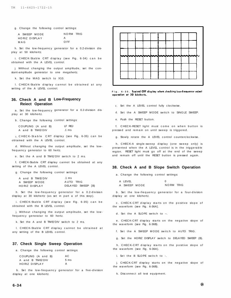
TM 11-6625-1722-15
g. Change the following control settings:
A SWEEP MODE N O R M T R I G
H O R I Z D I S P L A Y A
M A G O F F
h. Set the low-frequency generator for a 0.2-division dis-play at 50 kilohertz.
i . CHECK-Stable CRT display (see F ig. 6-34) can beobtained with the A LEVEL control.
j. Without changing the output amplitude, set the con-
stant-amplitude generator to one megahertz.
k. Set the MAG switch to X10.
l . CHECK-Stable display cannot be obtained at anysetting of the A LEVEL control.
36. Check A and BReiect Operation
a. Set the low-frequencyplay at 30 kilohertz.
b. Change the following
COUPLING (A and B)A and B TIME/DIV
C H E C K - S t a b l e C R T
Low-Frequency
generator for a 0.2-division dis-
control settings:
LF REJ.1 ms
display (see Fig. 6-35) can bec.obtained with the A LEVEL control.
d. Without changing the output amplitude, set the low-
frequency generator to 60 hertz.
e. Set the A and B TIME/DIV switch to 2 ms.
f. CHECK-Stable CRT display cannot be obtained at any
setting of the A LEVEL control.
g. Change the following control settings:
A and B TIME/DIV .1 ms
A SWEEP MODE A U T O T R I G
H O R I Z D I S P L A Y DELAYED SWEEP [B)
h. Set the low-frequency generator for a 0.2-divisiandisplay at 30 kilohertz (as set in part a of this step).
i . CHECK-Stable CRT display (see F ig. 6-35) can be
obtained with the B LEVEL control.
j. Without changing the output amplitude, set the low-frequency generatar to 60 hertz.
k. Set the A and B TIME/DIV switch to 2 ms.
l . CHECK-Stable CRT display cannot be obtained atany setting of the B LEVEL control.
37. Check Single Sweep Operation
a. Change the following control settings:
COUPLING (A and B) AC
A and B TIME/DIV 5 ms
H O R I Z D I S P L A Y A
b. Set the low-frequency generator for a five-divisiondisplay at one kilohertz.
6-34
F i g . 6 - 3 5 . Typical CRT display when checking Iow-freauencv reiectoperation at 30 kilohertz.
c.
d.
e.
f.
Set the A LEVEL control fully clockwise.
Set the A SWEEP MODE switch to SINGLE SWEEP.
Push the RESET button.
CHECK-RESET l ight must come on when button i spressed and remain on until sweep is triggered.
g. Slowly rotate the A LEVEL control counterclockwise.
h. CHECK-A single-sweep display (one sweep only) ispresented when the A LEVEL control is in the triggerableregion. RESET light must go off at the end of the sweepand remain off until the RESET button is pressed again.
38. Check A and B Slope Switch Operation
a. Change the following control settings:
A LEVEL 0
A SWEEP MODE N O R M T R I G
b. Set the low-frequency generator for a four-divisiondisplay at one kilohertz.
c. CHECK-CRT display starts on the pos i t ive s lope ofthe waveform (see Fig. 6-36A].
d. Set the A SLOPE switch to –.
e. CHECK-CRT display starts on the negative slope ofthe waveform (see Fig. 6-36B).
f . Set the A SWEEP MODE switch to AUTO TRIG.
g. Set the HORIZ DISPLAY switch to DELAYED SWEEP (B).
h. CHECK-CRT display starts on the pos i t ive s lope ofthe waveform (see Fig. 6-36A).
i . Set the B SLOPE switch to - .
j. CHECK-CRT display starts on the negative slope ofthe waveform (see Fig. 6-36B).
k. Disconnect all test equipment.

TM 1l-6625-1722-15
F i g . 6 - 3 6 . Typical CRT display when checking dopo switch opom-fbn. (A) SLOPE switch sot to +, (B) SLOPE swikh sot to -.
39. Check A and B Level Control Range
a. Connect the Iaw-frdquency generator to the B EXTTRIG INPUT connector through a 42-inch BNC cable andthe BNC T connector. Connect the output of the BNC Tconnector to the Channel 1 INPUT connector through an 18-inch BNC cable.
b. Change the following control settings:
Cl-f 1 VOLTS/DIV 1COUPLING (A and B) DCLEVEL (A and B) M i d r a n g eB SOURCE EXT
c. Set the low-frequency generator for a four-divisiondisplay [four volts peak to peak) at one kilohertz.
d. CHECK—Rotate the B LEVEL control throughout itsrange and check that display can be triggered (stable dis-play) at any point along the negative slope of the waveform(indicates B LEVEL cantrol range of at least + and – twavabs). Display is not triggered at either extreme of ratation.
e. Set the B SLOPE switch to +.
f. Cl-lECK-Rotate the B LEVEL control throughout itsrange and check that display can be triggered at any pointalong the positive slope of the waveform. Display is nottriggered at either extreme of rotation.
g. Set the CH 1 VOLTS/DIV switch to 10.
h. Set the B SOURCE switch to EXT + 10.
i. Set the low-frequency generator for a four-divisiondisplay (40 volts peak to peak) at one kilohertz.
j. CHECK-Rotate the B LEVEL control throughout itsrange and check that display can be triggered at any pointalong the positive slope of the waveform (indicates B LEVELcontrol range of at least + and -20 volts). Display is nottriggered at either extreme of rotation.
k. Set the B SLOPE switch to -.
l. CHECK-Rotate the B LEVEL control throughout itsrange and check that display can be triggered at any pointalong the negative slope of the waveform. Display is nottriggered at either extreme of rotation.
m. Change the following central settings:
A SOURCE EXT ÷ 10
A SWEEP MODE NORM TRIGHORIZ DISPLAY A
n. Disconnect the low-frequency generator from the BEXT TRIG INPUT connector and reconnect it to the A EXTTRIG INPUT connector.
a. CHECK-Rotate the A LEVEL control throughout itsrange and check that display can be triggered at any pointalong the negative slope af the waveform (indicates A LEVELcontrol range af at least + and - 20 volts). Display is nottriggered at either extreme of rotation.
p. Set the A SLOPE switch to +.
q. CHECK-Rotate the A LEVEL control throughout itsrange and check that display can be triggered at any pointalong the positive slope of the waveform. Display is nottriggered at either extreme of rotation.
r. Change the following control settings:
CH 1 VOLTS/DIV 1A SOURCE EXT
s. Set the low-frequency generator for a four-divisiondisplay (four volts peak to peak) at one kilohertz.
t. CHECK-Rotate the A LEVEL control throughout itsrange and check that display can be triggered at any pointalong the positive slope of the waveform (indicates A LEVELcontrol range of at least + and - two volts). Display isnot triggered at either extreme of rotation.
u. Set the A SLOPE switch to -.
v. CHECK-Rotate the A LEVEL control throughout itsrange and check that display can be triggered at any pointalong the negative slope of the waveform. Display is nottriggered at either extreme of rotation.
w. Disconnect all test equipment.
40. Check A and B line Triggering Operation
a. Connect the 10X probe to the Channel 1 INPUT con-nector.
6 - 3 5

TM 11-6625-1722-15
b. Change the following
CH 1 VOLTS/DIVSOURCE (A and B)A and B TIME/DIV
control settings: d. CHECK-Stableslope.
10LINE
e. Set the HORIZ
2 ms(B).
f. CHECK-Stable
CRT display triggered on the correct
DISPLAY switch to DELAYED SWEEP
CRT display triggered on the correct
c. Connect the probe tip to the same line-voltage sourceslope.
which is connected to this instrument. g. Disconnect all test equipment.
CRT controls
INTENSITYFOCUSSCALE ILLUM
Vertical controls (both
VOLTS/DIVVARIABLEPOSITIONInput CouplingMODETRIGGERINVERT
F i g . 6 - 3 7 . Initial test equipment setup for steps 41 through 60
MidrangeAdjust far focusedAs desired
channels if applicable)
.2CALMidrangeDCCH 1NORMPushed in
COUPLINGSOURCE
display Sweep controls
DELAY-TIME MULTIPLIERA and B TIME/DIVA VARIABLEA SWEEP MODEB SWEEP MODE
HORIZ DISPLAYMAGA SWEEP LENGTHPOSITIONPOWER
Triggering controls (both A and B if applicable) Side-panel controls
LEVEL Stable display B TIME/DIV VARIABLESLOPE + CALIBRATOR
ACI N T
Fully counterclockwise50 µsCALAUTO TRIGB STARTS AFTER
DELAY-TIMEAOFFFULLMidrangeON
CAL.1 V
6 - 3 6

6-37
TM 1l-6625-1722-15
41. Check Auto Recovery T ime and Operat ion
a. Test equipment setup is shown in Fig. 6-37.
b. Connect the time-mark generator to the Channel 1INPUT connector through the 42-inch 50-ohm BNC cableand 50-ohm BNC termination.
c. Set the time-mark generator for 50-millisecond markers.
CAUTION
To prevent permanent damage to the CRT phos-phor at slow sweep rates, position the baselineof the marker display below the viewing area.
d. CHECK-Stable display can be obtained with the ALEVEL control. Marker must be at the start af the sweep.
e. Set the time-mark generator for 0.1-second markers.
f. CHECK-Sweep free runs and stable display cannotbe obtained. If stable display is obtained, marker must notbe at the start of the sweep.
4 2 . A d j u s t S w e e p S t a r t a n d A S w e e pCal ibrat ion
A TIME/DIV 1 msB TIME/DIV 5 µsHORIZ DISPLAY A INTEN DURING B
b. Turn the DELAY-TIME MULTIPLIER dial fully counter-clockwise.
c. CHECK-DELAY-TIME MULTIPLIER dial setting 0.20.
d. ADJUST-If the DELAY-TIME MULTIPLIER dial is notcorrectly positioned when fully counterclockwise, Ioosen theset screw and reposition the dial to 0.20.
e. Repeat parts b through d until the DELAY-TIME Multi-plier dial is correctly positioned at 0.20.
f. Set the time-mark generator for one-millisecond markers.
g. Set the DELAY-TIME MULTIPLIER dial to 1.00.
h. CHECK-lntensified portion of display starts at secandmarker (see Fig. 6-38A).
i. ADJUST-Sweep Start adjustment, R758 (see Fig. 6-38C),so intensified portion starts at second marker (preliminaryadjustment).
j. Set DELAY-TIME MULTIPLIER dial to 9.00.
k. CHECK-lntensified portion of display starts at tentha. Change the following control settings: marker (see Fig. 6-38B).
F i g . 6 - 3 8 . (Al Typical CRT display showing intensified portion correctly located at the second marker, (S1 typical CRT display showinglntscnslfred portian correctly located at the tenth marker, (C) location of Sweep Start and A Sweep Cal adjustments (B Sweep board), ID)fypicai CRT display showing correct final adjustment of Sweep Start and A Sweep Cal da~ustments.

TM 11-6625-1722-15
1. ADJUST-A Sweep Cal adjustment, R531 (see Fig. 6-38C), so intensified portion starts at tenth marker (preliminaryadjustment].
m. Set the HORIZ DISPLAY switch to DELAYED SWEEP (B).
n. Set the DELAY-TIME MULTIPLIER dial to 1.00.
o. CHECK-Displayed pulse starts at the beginning of thesweep (see Fig. 6-38 D).
p. ADJUST-Sweep Start adjustment, R758 (see Fig. 6-38C),so displayed pulse starts at the beginning of the sweep.
q. Set DELAY-TIME MULTIPLIER dial to 9.00.
r. CHECK-Displayed pulse starts at the beginning of thesweep (see Fig. 6-38D).
s. ADJUST-A Sweep Cal adjustment, R531 (see Fig.6-38C), so displayed pulse starts at the beginning of thesweep.
t.
4 3 .
Recheck parts n through s and readjust if necessary.
A d j u s t N o r m a l G a i n
F i g . 6 - 3 9 . (Al Typical CRT display showing correct normal gain;[6) location of Normal Gain adjustment (B Sweep circuit board) .
6 - 3 8
b. CHECK-CRT display for one marker each divisionbetween the first-and ninth-division vertical lines (see Fig.6-39A).
NOTE
Unless otherwise noted, use the middle eight hori-zontal divisions when checking or adjusting timing.
c. ADJUST-Normal Gain adjustment, R835 (see Fig. 6-39B), for one marker each division. The second and tenthmarkers must coincide exactly with their respective graticulelines (repositian the display slightly with the horizontal POSl-TION control if necessary).
d. iNTERACTION-Check
4 4 . A d j u s t M a g n i f i e d
steps 44-59.
G a i n
a. Set the time-mark generator for 0.1 millisecond markers.
b. Set the MAG switch to X10.
c. CHECK-CRT display for one marker each divisionbetween the first and ninth graticule lines (see Fig. 6-40A).
F ig . 6 -40. (A) Typical CRT display showing correct magnified gain;(B) location of Mccg Gain adjustment ( B Sweep circuit board).

TM 11-6625-1722-15
d. ADJUST-Mag Gain adjustment, R845 (see Fig. 6-40B),for one marker each division. The second and tenth markersmust coincide exactly with their respective graticule lines(reposition the display slightly with the horizontal FINEcontrol if necessary).
e. Position the first eight-division portion of the totalmagnified sweep onto the viewing area.
f. CHECK-One marker each division between the first-and ninth-division vertical lines; marker at ninth-divisionvertical line must be within 0.12 division (within 1.5%) of theline when the marker at the first-division vertical line ispositioned exactly.
g. Repeat this check for each eight division portion ofthe total magnified sweep length.
h. INTERACTION-Check steps 45, 53, 55 and 57.
4 5 . A d j u s t M a g n i f i e r R e g i s t e r
a. Set the time-mark generator for five-millisecond markers.
b. Position the middle marker (three markers on total mag-nified sweep) to the center vertical line (see Fig. 6-41A).
c. Set the MAG switch to OFF.
d. CHECK-Middle marker should remain at the centervertical line (see Fig. 6-41B).
e. ADJUST-Mag Register adjustment, R855 (see Fig. 6-41C], to position the middle marker to the center vertical line.
f. Set the MAG switch to X10.
g. Repeat parts b through e until no shift occurs whenMAG switch is set to OFF.
4 6 . A d j u s t B S w e e p C a l i b r a t i o n
a. Change the following control settings:
DELAY-TIME MULTIPLIER Fully counterclockwiseA TIME/DIV 2 msB TIME/DIV 1 msB SWEEP MODE TRIGGERABLE AFTER
DELAY TIMEHORIZ DISPLAY DELAYED SWEEP (B)MAG OFF
b. Set the time-mark generator for one-millisecond markers.
c. Set the B LEVEL control for a stable display.
d. CHECK-CRT display for one marker each division.between the first- and ninth-division vertical lines (see Fig.6-42A].
e. ADJUST-B Sweep Cal adjustment, R741 (see Fig. 6-42B),for one marker each division.
f. INTERACTION-Check steps 51 and 56.
4 7 . C h e c k B S w e e p L e n g t h
a. Set the time-mark generator for 1- and 0.1-millisecondmarkers.
b. Move the eleventh large marker to the center verticalline with the horizontal POSITION control (see Fig. 6-43).
F ig . 6 -41. Typical CRT display showing correct magnif Ior mglster.(A) MAG switch ta x 10, (B) MAG switch set to OFF, [C) loca-tian of Mag Register adjustment (B Sweep circuit board).
c. CHECK-B Sweep length must be between 10.5 and11.5 divisions, as shown by 0.5 to 1.5 divisions of display tothe right of the center vertical line (see Fig. 6-43). Largemarkers indicate divisions and small markers indicate 0.1division.
4 8 . C h e c k A S w e e p L e n g t h
a. Set the HORIZ DISPLAY switch to A.
b. Set the A TIME/DIV switch to 1 ms.
6 - 3 9

Fig. 6-44
TM 11-6625-1722-15
F i g . 6 - 4 2 . (A) Typical CRT display showing correct B Sweep cali-bration, (B) location of the B Sweep Cccl adjustment of (B Sweepcircuit board] .
c. Move the eleventh marker to the center vertical linewith the horizontal POSITION control (see Fig. 6-43].
d. CHECK-A Sweep length must be between 10.5 and11.5 divisions as shown by 0.5 to 1.5 divisions of display tothe right of the center vertical line.
e. Reposition the first marker to the left graticule line.
f. Turn the A SWEEP LENGTH control to 4 DIV (not in BENDS A detent).
g. CHECK-A Sweep length must be four divisions or less.
49. Check B Ends A Operation
a. Change the following control settings:
B TIME/DIV .1 msB SWEEP MODE B STARTS AFTER
DELAY TIMEHORIZ DISPLAY A INTEN DURING BA SWEEP LENGTH B ENDS A
b. Rotate the DELAY-TIME MULTIPLIER dial throughout itsrange.
c. CHECK-CRT display ends after the intensified portionat 011 DELAY-TIME MULTIPLIER dial settings.
F i g . 6 - 4 3 . Typical CRT display when checking A and B sweepIenglh.
50. Check A Variable Control Range
a. Change the following control settings:
DELAY-TIME MULTIPLIER Fully counterclockwiseB TIME/DIV 1 msHORIZ DISPLAY AA SWEEP LENGTH FULL
b. Set the time-mark generator for 10-millisecond markers.
c. Position the markers to the far left and right graticulelines with the horizontal POSITION control.
d. Turn the A VARIABLE control fully counterclockwise.
e. CHECK-CRT display for four-division maximum spacingbetween markers (indicates adequate range for continuouslyvariable sweep rates between the calibrated steps; see Fig.6-44). UNCAL A OR B light must be on when A VARIABLEcontrol is not in CAL position.
6-40

TM 11-6625-1722-15
5 1 . C h e c k B V a r i a b l e C o n t r o l R a n g e
a. Change the following control settings:
A TIME/DIV 5 ms
B TIME/DIV 1 ms
A VARIABLE CAL
B SWEEP MODE TRIGGERABLE AFTERDELAY TIME
HORIZ DISPLAY DELAYED SWEEP (B)
b. Position markers to the far left and right vertical linesof the graticule with the horizontal POSITION control.
c. Turn the B TIME/DIV VARIABLE control fully counter-clockwise.
d. CHECK-CRT display for four-division maximum spacingbetween markers (indicates adequate range for continuouslyvariable sweep rate between the calibrated steps; see Fig.6-44). UNCAL A OR B light must be on when B TIME/DIVVARIABLE control is not in CAL position.
5 2 . A d j u s t O n e - M i c r o s e c o n d T i m i n g
a. Change the following control settings:
A and B TIME/DIV 1 µs
HORIZ DISPLAY A
B TIME/DIV VARIABLE CAL
b. Set the time-mark generator for one-microsecond mark-ers.
c. CHECK-CRT display for one marker each divisionbetween the first- and ninth-division vertical lines (see Fig.6-45A).
d. ADJUST-C530A (see Fig. 6-45B) for one marker eachdivision.
e. Set the HORIZ DISPLAY switch to DELAYED SWEEP (B].
F i g . 6 - 4 5 . Twsical CRT disrslcw showing correct one-microsecondti;ing, (B) - “location of CS30A and ~740A (behind swing-outside panel).
f. CHECK-CRT display for one marker each divisionbetween the first- and ninth-division vertical lines (see Fig.6-45A).
g. ADJUST-C740A (see Fig. 6-45B) for one marker eachdivision.
N O T E S
6 - 4 1

TM 11-6625-1722-15
F i g . 6 - 4 6 . (A) Typical CRT dissdav showirw correct hiah moodIirmarity, (B] loca~on of C882 and- C892 (B-Sweep circu~ bo&dl.
53. Adjust High-Speed Linearity o
a. Change the following control settings:
CH 1 VOLTS/DIV 20 mVA ond B TIME/DIV .1 pHORIZ DISPLAY A
b. Set the time-mark generator for 10-nanosecond markers.
c. Position the display horizontally so the sweep startsat the left edge of the graticule.
d. Set the MAG switch to X 10.
e. CHECK-CRT display for optimum linearity over thecenter eight divisions of the graticule (see Fig. 6-46A).
f. ADJUST-C882 and C892 (see Fig. 6-46B) for optimumlinearity over the center eight divisions of the graticule (at-tempt to keep C882 and C892 nearly equal in capacitanceby adjusting each capacitor about the same amount).
54. Check A Sweep
a. Change the following
6-42
liming Accuracy
control settings:
CH 1 VOLTS/DIV .2
MAG OFF
b. CHECK-Using the A TIME/DIV switch and time-markgenerator settings given in Table 6-5, check A sweep timingwithin 0.24 division, over the middle eight divisions of thedisplay (within 3%).
CAUTION
To prevent possible burning of the CRT phosphorat slow sweep rates, position the baseline of themarker display below the viewing area.
TABLE 6-5
A and B Timing Accuracy
55. Check A Magnified Sweep Accuracy
a. Set the MAG switch to X 10.
b. CHECK-Using the A TIME/DIV switch and time-markgenerator settings given in Table 6-6, check A magnifiedsweep timing within 0.32 divisions over the middle eightdivisions of the magnified display (within 4%). Note the por-tion of the total magnified sweep length to be excluded fromthe measurement. Magnifier light must be on.

TM 1 1 - 6 6 2 5 - 1 7 2 2 - 1 5
TABLE 6-6
A and B Magnified Accuracy
A and B Time-Mark CRT Display Portions of total magnifiedT IME/DIV Generator Output (markers/ sweep length to exclude
Switch Setting division) from measurement
.1 µs 10 nanosecond 1 First and last three divisions.
.2 µs 10 nanosecond 2 First and last 3.5 divisions.
.5 µs 50 nanosecond 1 First two divisions.
1 µs 0.1 microsecond 1 First division.
2 µs 0.1 microsecond 2
5 µ s 0.5 microsecond 1
1 0 µ s 1 microsecond 1
20 µs 1 microsecond 2
50 µs 5 microsecond 1
.1 ms 10 microsecond 1
.2 ms 10 microsecond 2
.5 ms 50 microsecond 1
1 ms 0.1 millisecond 1
2 ms 0.1 millisecond 2
5 ms 0.5 millisecond 1
10ms 1 millisecond 1
20 ms 1 millisecond 2
50 ms 5 millisecond 1
.1 s 10 millisecond 1
.2 s 10 millisecond 2
.5 s 50 millisecond 1
A Sweep Only
1 s 0.1 second 1
2 s 0.1 second 2
5 s 0.5 second 1
5 6 . C h e c k B S w e e p T i m i n g A c c u r a c y
a. Set the MAG switch to OFF.
b. Set the HORIZ DISPLAY switch to DELAYED SWEEP (B).
c. CHECK-Using the A and B TIME/DIV switch and time-mark generator settings given in Table 6-5, check B sweeptiming within 0.24 division over the middle eight divisions
of the display (within 3%).
5 7 . C h e c k B M a g n i f i e d S w e e p A c c u r a c y
a. Set the MAG switch to X10.
b. CHECK-Using the A and B TIME/DIV switch and time-mark generator settings given in Table 6-6, check B magni-fied sweep timing within 0.32 division over the middle eightdivisions of the magnified display (within 4%). Note theportions of the total magnified sweep length to be excludedfrom the measurement.
5 8 . C h e c k D e l a y - T i m e A c c u r a c y
a. Set the MAG switch to OFF.
b. Set the B SWEEP MODE switch to B STARTS AFTERDELAY TIME.
c. CHECK-Using the A TIME/DIV switch, B TIME/DIVswitch and time-mark generator settings given in Table 6-7,check delayed sweep accuracy within the given tolerance.First set the DELAY-TIME MULTIPLIER dial to 1.00 and rotatethe dial until the sweep starts at the top of the secondmarker (see Fig. 6-47). Note the dial reading and then setthe dial to 9.00 and rotate until the sweep starts at the topof the tenth marker. DELAY-TIME MULTIPLIER dial settingmust be 8.00 divisions higher; + or - the allowable errorgiven in Table 6-7.
NOTE
Sweep will start at top of third marker at 1.00, andnineteenth marker at 9.00 for sweep rates whichare multiples of 2 (e.g., 2 µs, 20 µs, .2 ms, etc.).If in doubt as to the correct setting af the DELAY-TIME MULTIPLIER dial, set the HORIZ DISPLAYswitch to A INTEN DURING B and check whichmarker is intensified.
6 - 4 3

59.
TM 11-6625-1722-15
TABLE 6-7
Delayed Sweep Accuracy
A T IME/DIV B TIME/DIV Time-Mark Allowable error forSwitch Setting Switch Setting Generator Output given accuracy
1 µs .1 µs 1 microsecond–
2 µs .1 µs 1 microsecond
5 µs .5 µs 5 microsecond10 µs 1 µs 10 microsecond
20 µs 1 µs 10 microsecond
50 µs 5 µs 50 microsecond.1 ms 10 µs 0.1 millisecond ±12 minor dial divisions.2 ms 10 µs 0.1 millisecond (±1.5% over center eight.5 ms 50 µs 0.5 millisecond divisions)
1 ms .1 ms 1 millisecond2 ms .1 ms 1 millisecond
5 ms .5 ms 5 millisecond10 ms 1 ms 10 millisecond
20 ms 1 ms 10 millisecond
50 ms 5 ms 50 millisecondI.1 s 10 ms 0.1 second
.2 s 10 ms 0.1 second
.5 s 50 ms 0.5 second±20 minor dial divisions
1 s .1 s 1 second(±2.5% over center eightdivisions]
2 s I .1 s I 1 second1 I5 s .5 s 5 second
Delay-T ime Mul t ip l ie r IncrementalL inear i ty
a. Change the following control settings:
DELAY-TIME MULTIPLIER 9.00
A TIME/DIV 1 ms
B TIME/DIV 5 µs
b. Set the time-mark generator for one-millisecond markers.
c. Rotate the dial as necessary to position the start of thepulse to the beginning of the sweep (see Fig. 6-48).
d. CHECK-Deviation of dial reading from 9.00 shouldbe within two minor dial divisions (±0.2%).
NOTE
A sweep must be correctly calibrated to check thisstep to the given accuracy.
e. Repeat check at each major dial division between 9.00and 1.00.
F ig . 6 -47. Typical CRT display when checking delayed-sweep accu-racy.
6 - 4 4
F i g . 6 - 4 8 . Typical CRT display when checking DELAY-TIME Multi-plier incremental linearity.

TM 11-6625-1722-15
60. Check Delay-Time Jitter
a. Change the following control settings:
b. Position the pulse near the center of the display areawith
c.
the DELAY-TIME MULTIPLIER dial.
1.001 µs
CHECK-Jitter on the leading edge of the pulse shouldnot exceed 0.5 division (one part in 20,000; see Fig. 6-49).Disregard slow drift.
d. Turn the DELAY-TIME MULTIPLIER dial to 9.00 and ad-just so the pulse is displayed near the center of the displayarea.
e. CHECK-Jitter on leading edge of the pulse shouldnot exceed 0.5 division (see Fig. 6-49]. Disregard slow drift.
f. Disconnect all test equipment. F i g . 6 - 4 9 . Typical CRT display when checking delay-timo Iittor,
N O T E S
6 - 4 5

TM 11-6625-1722-15
F i g . 6 - 5 0 . Initial to$t l quipmwtt setup for steps 61 through 66.
CRT controls HORIZ DISPLAY EXT HORIZ
INTENSITYFOCUSSCALE ILLUM
MidrangeMAG OFF
Adjust for focused displayA SWEEP LENGTH FULL
As desiredPOSITION MidrangePOWER O N
Vertical controls (both channels if applicable)
VOLTS/DIV 20 mVVARIABLE CALPOSITION MidrangeINPUT COUPLING DCMODE CH 2TRIGGER CH 1 ONLYINVERT Pushed in
Triggering controls (both A ond B if applicable)
LEVEL Any positionSLOPECOUPLING DCSOURCE INT
Sweep controls
DELAY-TIME MULTIPLIER 9.00A TIME/DIV 1 msB TIME/DIV 1 msA VARIABLE CALA SWEEP MODE AUTO TRIGB SWEEP MODE B STARTS AFTER
DELAY TIME
Side-panel controls
B TIME/DIV VARIABLE CALCALIBRATOR .1 v
61. Adjust External Horizontal Gain o
a. Test setup is shown in Fig. 6-50.
b. Connect the standard amplitude calibrator to the Chan-nel 1 INPUT connector through the 42-inch BNC cable.
c. Set the standard amplitude calibrator for a 0.1 -voltsquore-wave output.
d. Increase the INTENSITY control setting until the displayis visible (two dots about five divisions apart).
e. Move the display to the center of the graticule with theChannel 1 POSITION control.
f. CHECK-CRT display for five divisions horizontal deflec-tion. (See Fig. 6-51A).
g. ADJUST-Ext Horiz Gain adjustment, R645 (see Fig.6-51B), for five divisions horizontal deflection.
6-46 @

TM 11-6625-1722-15
F i g . 6 - 5 1 . (Al Typical CRT display showing correct external hori-xorstal ~ain, (B) location of Ext Horlz Gain adjustment (B Sweepsfscult bed).
6 2 . C h e c k E x t e r n a l H o r i z o n t a l O p e r a t i o n
a. Set the B SOURCE switch to EXT.
b. Connect the standard amplitude calibrator to the EXTHORIZ input connector (B EXT TRIG INPUT).
c. Set the standard amplitude calibrator for a two-voltsquare-wave output.
d. CHECK-CRT display for horizontal deflection between6.5 and 8.7 divisions (270 millivolts/division, ±15%).
e. Set the standard amplitude calibrator for a 20-voltsquare-wave output.
f. Set the 8 SOURCE switch to EXT ÷ 10.
g. CHECK-CRT display for horizontal deflection between6.2 and 9.2 divisions (2.7 voIts/division,
h. Disconnect all test equipment.
6 3 . C h e c k X - Y P h a s i n g
÷ 2 0 % ) .
a. Connect the constant-amplitude sine wave generator tothe Channel 1 and 2 INPUT connectors through the five-nanosceond GR cable, 50-ohm in-line termination and thedual-input coupler.
F i g . 6 - 5 2 . Typical CRT display when checking X-Y phasing,
b. Change the following control settings:
CH 1 VOLTS/DIV 10 mVCH 2 VOLTS/DIV 50 mVB SOURCE INT
c. Set the medium-frequency generator for a 10-divisionhorizontal display at 50 kilohertz.
d. Center the display vertically and horizontally with theChannel 1 and 2 POSITION controls.
e. CHECK-CRT display for an opening at the center hori-zontal line of 0.52 division or less (3° or less phase shift; seeFig. 6-52).
6 4 . C h e c k X B a n d w i d t h i n E x t e r n a l H o r i z o n t a lM o d e
a. Disconnect the dual-input coupler from the Channel 2INPUT connector.
b. Set the medium-frequency generator for a six-divisionhorizontal display at its reference frequency (50 kHz).
c. Without changing the output amplitude, increase theoutput frequency of the generator until the horizontal deflec-tion is reduced to 4.2 divisions (-3 dB point; see Fig. 6-53).
d. CHECK-Output frequency of generator must be fivemegahertz or higher.
6 5 . C h e c k T r a c e F i n d e r O p e r a t i o n
a. Reconnect the dual-input coupler to the Channel 2INPUT connector.
b. While holding the TRACE FINDER button depressed,rotate the Channel 1, Channel 2 and horizontal POSITIONcontrols and the CH 1 and CH 2 VOLTS/DIV switchesthroughout their ranges.
c. CHECK-CRT display remains within the graticule area.
d. While holding the TRACE FINDER button depressed,adjust the positioning controls until the display is centeredabout the graticule center lines. Then, increase the X and Y
6 - 4 7

TM 11-6625-1722-15
F i g . 6 - 5 3 . Typical CRT display when checking external horizontalbandwidth ( double exposure) .
deflection factors until the display is reduced to about twodivisions vertically and abaut four divisions horizontally.
e. Release the TRACE FINDER button.
f. CHECK-CRT display must remain within the graticulearea.
g. Reduce the INTENSITY control to a normal setting (aboutmidrange).
h. Disconnect all test equipment.
6 6 . C h e c k C h o p p e d O p e r a t i o n
a. Change the following control settings:
Fig.rate
b.
6 - 5 4 . Typical CRT display when checking chopped repetitionand blanking.
MODE CHOPTRIGGER NORMA and B TIME/DIV .5 µsHORIZ DISPLAY A
Position the traces about four divisions apart.
c. Set the A LEVEL control for a stable display.
d. CHECK-Each cycle for duration of 3.4 to 5 divisio(500 kilohertz, ±20%; see Fig. 6-54).
e. CHECK-CRT display for complete blanking of switchingtransients between chopped segments (see Fig. 6-54).
6 - 4 8

TM ll-6625-1722-15
F i g . 6 - 5 5 . Initial test oquipm.nt setup for stops 67 through 70.
CRT controls
INTENSITY MidrangeF o c u s Adjust for focused displaySCALE ILLUM As desired
Vertical controls (both channels if applicable)
CH 1 VOLTS/DIV 50 mVCH 2 VOLTS/DIV .2VARIABLE CALPOSITION MidrangeInput Coupling DCMODE A L TTRIGGER NORMINVERT Pushed in
Triggering controls (both A and B if applicable)
LEVEL Stable displaySLOPECOUPLING ACSOURCE INT
Sweep controls
DELAY-T IME MULT IPL IER 9 .00A and B TIME/DIV 1 msA VARIABLE CALA SWEEP MODE AUTO TRIGB SWEEP MODE B STARTS AFTER
DELAY TIME
HORIZ DISPLAYMAGA SWEEP LENGTHPOSITIONPOWER
Side-panel controls
B TIME/DIV VARIABLECALIBRATOR
67. Adjus t Cal ib rator Repet i t ion Rate
AOFFFULLMidrangeO N
CAL.1 V
a. Test equipment setup is shown in Fig. 6-55.
b. Connect the 1 kHz CAL connector to theINPUT connector with an 18-inch BNC cable.
c. Connect the time-mark generator to theINPUT connector with a 42-inch BNC cable.
Channel 1
Channel 2
d. Set the time-mark generator for one-millisecond markers.
e. Position the display so the tips of the markers fall iustbelow the rising portions of the square wave (see Fig. 6-56A).
f. CHECK-For one cycle of calibrator waveform for eachmarker (see Fig. 6-56A).
g. ADJUST-Calibrator Frequency adjustment, T1255 (seeFig. 6-56B), for one cycle of calibrator waveform for eachmarker (preliminary adjustment).
6 - 4 9

Fig. 6-58
Fig. 6-57
TM 11-6625-1722-15
Fig. 6-56. (Al Typical CRT display showing correct calibrator repe-tition rate, (B] locat ion of Ca l ibra tor Frequency ccdiustment.
h. Set the TRIGGER switch to CH 1 ONLY.
i. CHECK-CRT display for slow drift or no drift of thetime markers.
j. ADJUST-T1255 for minimum drift of time markers.(final adjustment).
k. Disconnect the time-mark generator.
68. Check Calibrator Duty Cycle
a. Change the following control settings:
CH 1 VOLTS/DIV 20 mVMODE CH 1A and B TIME/DIV .1 ms
b. Center the display vertically with the Channel 1 POSl-TION control.
c. Set the A LEVEL control so the display starts at the50% point on the rising portion of the waveform (the INTEN-SITY control may need to be advanced slightly to see therising portion of the waveform).
d. Set the MAG switch to X 10.
6-50
e. Position the 50% point on the falling edge of the Cali-brator waveform to the center vertical line.
f. Set the A SLOPE switch to -.
g. CHECK-50% point on rising edge now displayed notdisplaced more than two divisions from the center verticalline (duty cycle 49% to 51%; see Fig. 6-57).
69. Check Calibrator Risetime
a. Change the following control settings:
A SLOPE +A and B TIME/DIV .2 psMAG OFF
b. Set the A LEVEL control so all of the rising portion ofthe Calibrator waveform is visible.
c. Position the 10% point on the leading edge to a verti-cal graticule line.
d. CHECK-CRT display for five divisions or less betweenthe 10% and 90% points an the leading edge of the cali-

TM 11-6625-1722-15
F i g . 6 - 5 9 . Typical CRT display when chocking calibrator current.
brator waveform (one microsecond or less, risetime; see Fig.6-58).
e. Disconnect the 18-inch BNC cable.
7 0 . C h e c k C u r r e n t t h r o u g h P r o b e L o o p
a. Connect the current-measuring probe and passive termi-nation to the Channel 1 INPUT connector.
b. Set the passive termination for a sensitivity of 2mA/mV.
c. Clip the current probe around the PROBE LOOP on theside panel.
d. Set the CH 1 VOLTS/DIV switch to 5 mV.
e. Set the A and B TIME/DIV switch to .5 ms.
f. CHECK-CRT display 0.5 division in amplitude (fivemilliseconds; see Fig. 6-59).
NOTE
This step checks for the presence of current in thePROBE LOOP. This current will remain within thestated 1% accuracy due to the tolerance of thedivider resistors and tolerance of the calibratoroutput voltage (adjusted in step 2). If it is nec-essary to verify the accuracy of the calibrator cur-rent, use a current measuring meter with an ac-curacy of at least 0.25%.
g. Disconnect all test equipment.
N O T E S
6 - 5 1

TM 11-6625-1722-15
F i g . 6 - 6 0 . Initial test equipmsnt setup for steps 71 through 74.
CRT controls
INTENSITY MidrangeFOCUS Adjust for focused displaySCALE ILLUM As desired
Vertical controls (both channels if applicable]
VOLTS/DIV 5 mVVARIABLE CALPOSITION MidrangeINPUT COUPLING DCMODE CH 1TRIGGER NORMINVERT Pushed in
Triggering controls (both A and B if applicable)
LEVEL 0SLOPECOUPLING ACSOURCE INT
Sweep controls
DELAY-TIME MULTIPLIER Fully counterclockwiseA and B TIME/DIV .1 µsA VARIABLE CALA SWEEP MODE AUTO TRIGB SWEEP MODE B STARTS AFTER
DELAY TIME
6 - 5 2
HORIZ DISPLAY AMAG OFFA SWEEP LENGTH FULLPOSITION MidrangePOWER ON
Side-panel controls
B TIME/DIV VARIABLE CALCALIBRATOR .1 V
71. Adjus t Z Axis Compensat ion
a. Test equipment setup is shown in Fig. 6-60.
b. Connect the 10X probe to the input connector of thetest oscilloscope.
c. Connect the 10X probe to TP1047 (see Fig. 6-61A).
d. Set the test oscilloscope for a vertical deflection factorof 0.5 volts/division (5 volts/division total with probe) at asweep rate of 0.1 microsecond/division.
e. Set the INTENSITY control so the test oscilloscope dis-play is three divisions in amplitude.
f. CHECK-Test oscilloscope display for optimum squarecorner (slightly rounded) on blanking gate (see Fig. 6-61B).
g. ADJUST-C1036 (see Fig. 6-61A) for optimum squarecorner on the unblanking gate.

TM 11-6625-1722-15
F i g . 6 - 6 1 . (A) Location of TP1 047 and Cl 036, (S) tvPical te!
oscilloscope display showing correct adjustment of Cl 036” [verticaldaflectiori, 5 volts/division, sweep rate, 0.1 microsecond/division )
h. Disconnect all test equipment.
72. Check External Z Axis Operation
a. Set the INTENSITY control to a normal setting.
b. Set the A and B TIME/DIV switch to 20 Ks.
c. Connect the constant-amplitude generator to the A EXTTRIG INPUT connector through the five-nanosecond GRcable, 50-ohm in-line termination and BNC T connector. Con-nect the output of the BNC T connector to the Z AXIS INPUTbinding posts through a 42-inch BNC cable and the BNCto alligator clips adapter. (Connect black lead af alligatorclips adapter to ground post.)
d. Set the A SOURCE switch to EXT.
e. Remove the ground strap from between the bindingposts.
f. Set the constant-amplitude generator for five voltsoutput at 50 kilohertz (use calibrated position of generatoramplitude control).
g. CHECK-CRT display for noticeable intensity modula-tion [see Fig. 6-62A). The INTENSITY control setting may needto be reduced to view trace modulation.
@
F i g . 6 . 6 2 . [A) Typical CRT display when checkh Z-axis aP@ratiOn
at 50 kilohertz, (B) typical CRT display when checking Z-axis op*r-ation at 50 megahertz.
h. Set the constant-amplitude generator for five voltsoutput at 50 megahertz [use calibrated position of generatoramplitude control).
i. Set the A and B TIME/DIV switch to .1 PS.
j. CHECK-CRT display for noticeable intensity modula-tion (see Fig, 6-62B). The INTENSITY control setting mayneed to be reduced to view trace modulation.
k.
73.
a.
b.
Disconnect all test equipment and replace ground strap.
Check A Gate Output Signal
Set the A and B TIME/DIV switch to 1 ms.
Connect the A GATE cannector (on side panel) to thetest-oscilloscope input connector with the 42-inch BNC cable.
c. Set the test oscilloscope for a vertical deflection factorof five volts/division at a sweep rate of twa milliseconds/division.
d. CHECK-Test oscilloscope display for 2.4 divisions;±0.24 division, vertical deflection with the bottom of thewaveform near the zero-volt level (12 volts, ±10%; seeFig. 6-63). Gate duration should be about 5.5 divisions(about 11 times the A TIME/DIV switch setting).
6-53

TM 11-6625-1722-15
F i g . 6 - 6 3 . Typical CRT disploy when checking gate amplitude andduration [vertical deflection, fivomilliseconds/division) .
volts /divis~on; sweep rate, two
74. Check B Gate Output Signala. Cannect the B GATE connector (on side panel) to the
test-oscilloscope input connector with the 42-inch BNC cable.
b. Change the following control settings:
A TIME/DIV 2 msB TIME/DIV 1 msHORIZ DISPLAY DELAYED SWEEP (B)
c. CHECK-Test oscilloscope display for 2.4 divisions,±0.24 division, vertical deflection with the bottom of the
waveform near the zero-volt level (12 volts ±10%; see Fig.6-63). Gate duration should be about 5.5 divisions (about11 times the B TIME/DIV switch setting).
This completes the calibration procedure for the Type 453.Disconnect all test equipment and replace the top and bottomcovers. If the instrument has been completely checked andcalibrated to the tolerances given in this procedure, it willmeet the electrical characteristics listed in the PerformanceRequirement column of the Characteristicsmanual.
section of this
NOTES
6-54

TM 11-6625-1722-15
S E C T I O N 7
P R E V E N T I V E M A I N T E N A N C E I N S T R U C T I O N S
7 - 1 . S c o p e o f M a i n t e n a n c e
The maintenance duties assigned to operator andorganizational categor ies are l i s t e d b e l o w ,
t o g e t h e r w i t h a r e f e r e n c e t o t h e p a r a g r a p h s
covering the specific maintenance functions.
a. Dai ly prevent ive maintenance checks and
services (para 7–4).
b. Weekly preventive maintenance checks and
services (para 7–5).
c. Monthly preventive maintenance checks and
services (para 7–6).
d. Quarter ly prevent ive maintenance checks
and services (para 7–7).
e. Cleaning (para 7–8).
f. Touchup pa int ing (para 7–9) .
7 - 2 . P r e v e n t i v e M a i n t e n a n c e
Prevent ive maintenance i s the sys temat ic care,
servicing, and inspection of equipment to prevent
the occurrence of trouble, to reduce downtime,
and to assure that the equipment is serviceable.
a. Sys temat ic Care. The procedures g iven inparagraphs 7–3 through 7–9 cover routine syste-
matic care and cleaning essential to proper up-
keep and operation of the equipment.
b. Prevent ive Maintenance Checks and Ser -vices. The prevent ive maintenance checks and
serv ices char t s (paras 7–4 th rough 7–7) out l inefunct ions to be per formed at speci f ic in terva l s .
These checks and services are to maintain Armyelectronic equipment in a combat-serviceable con-
d i t ion ; that i s , in good genera l (phys ica l ) con-
dit ion and in good operating condit ion. To ais ist
operators in maintaining combat serviceability, the
charts indicate what to check, how to check, andwhat the normal condit ions are; the R e f e r e n c e s
c o l u m n l i s t s t h e i l l u s t r a t i o n s , p a r a g r a p h s , o r
manuals that contain detai led repair or replace-
m e n t p r o c e d u r e s . I f t h e d e f e c t c a n n o t b e
remedied by the corrective actions l isted, higher
c a t e g o r y o f m a i n t e n a n c e r e p a i r i s r e q u i r e d .
Records and reports of these checks and services
must be made in accordance wi th the requi re-ments set for th in TM 38–750.
7 – 3 . P r e v e n t i v e M a i n t e n a n c e C h e c k sand Serv ices Per iods
Preventive maintenance checks and services of the
equipment are requ i red da i ly , week ly , month ly ,
and quarterly.
a. P a r a g r a p h 7 – 4 s p e c i f i e s t h e c h e c k s a n d
services that must be accomplished daily (or atleast once each week if the equipment is main-
tained in standby condition).
b. P a r a g r a p h s 7 – 5 , 7 – 6 , s n d 7 – 7 s p e c i f y
addit ional checks and services that must be per-
formed weekly, monthly, and quarterly.
7 - 4 . D a i l y P r e v e n t i v e M a i n t e n a n c e C h e c k s a n d S e r v i c e s C h a r t
Sequenceno.
1
2
3
4
Item to be inspected
Completeness . . . . . . . . . . . . .
Exterior surfaces. . . . . . . . . . .
Connectors . . . . . . . . . . . . . .
Controls . . . . . . . . . . . . . . . . .
Operation . . . . . . . . . . . . . . . .
Procedure
See that the equipment is complete (app. B).
Clean the exterior surfaces (para 7–8)
Check the tightness of all connectors.
While makhg the operating check (sequenceNo. 5), check to see that the mechanicalaction of each knob, dial, and switch issmooth and free of external or internalbinding, and that there is no excessivelooseness.
Operate the equipment according to section 2.
References
None.
7 - 1

TM 11-6625-1722-15
7 – 5 . W e e k l y P r e v e n t i v e M a i n t e n a n c e C h e c k s a n d S e r v i c e s C h a r t
Sequenceno. .
2
3
Item to be inspected
Cables and probes . . . . . . . . .
Handles and latches . . . . . . . .
Metal surfaces . . . . . . . . . . . .
Procedure References
Inspect cords, cables, probes, and wires forchafed, cracked, or frayed insulation.Replace connectors that are broken, arced,stripped, or worn excessively.
Inspect handles for looseness. Replace ortighten as necessary.
Inspect exposed metal surfaces for rust andcorrosion. Clean and touch up paint asrequired.
Paras 7–8 and 7-9.
7 – 6 . M o n t h l y P r e v e n t i v e M a i n t e n a n c e C h e c k s a n d S e r v i c e s C h a r t
Sequenceno.
1
2
3
4
5
6
7
Item to be inspected
Pluckout items . . . . . . . . . . .
Jacks . . . . . . . . . . . . . . . . . . .
Transformer terminals. . . . . .
Terminal blocks . . . . . . . . . .
Resistors and capacitors . . .
Variable capacitors . . . . . . . .
Interior . . . . . . . . . . . . . . . .
Procedure
Inspect seating of pluckout items.
Inspect jacks for snug fit and good contact.
Inspect terminals on the transformers. Thereshould be no evidence of dirt or corrosion.
Inspect terminal blocks for loose connectionsand cracked or broken insulation.
Inspect resistors and capacitors for cracks, blistering, or other defects.
Inspect variable capacitors for dirt, corrosion,and deformed plates.
Clean interior of chassis and cabinet.
7 – 7 . Q u a r t e r l y P r e v e n t i v e M a i n t e n a n c e C h e c k s a n d S e r v i c e s C h a r t
Sequenceno.
1
2
3
7 - 2
Item to be inspected
Publications . . . . . .
Modifications . . . . . . . . . .
Spare parts . . . . . .
—
Procedure
See that al l publications are complete,serviceable, and current.
Check DA Pam 310–7 to determine whethernew applicable MWO's have been published.Al l URGENT MWO'S must be appliedimmediately. All NORMAL MWO'S must bescheduled.
Check all spare parts (operator and org-anizational) for general condition andmethod of storage. No overstock should beevident, and all shortages must be on validrequisitions.
References
None.
References
DA Pam 310–4.
TM 38–750 andDA Pam 310–7.

TM 11-6625-1722-15
7 - 8 . C l e a n i n g
I n s p e c t t h e e x t e r i o r o f t h e e q u i p m e n t . T h e
exter io r su r faces shou ld be f ree of d i r t , g rease,
and fungus .
a . R e m o v e d u s t a n d o t h e r l o o s e d i r t w i t h a
clean soft cloth.W A R N I N G
A d e q u a t e v e n t i l a t i o n s h o u l d b e p r o -
v i d e d w h i l e u s i n g T R I C H L O R O T R I -
F L U O R O E T H A N E . P r o l o n g e d b r e a t h i n g o f
vapor should be avoided. The solvent should
not be used near heat or open f lame; the
p r o d u c t s o f d e c o m p o s i t i o n a r e t o x i c a n d
i r r i t a t i n g . S i n c e T R I C H L O R O T R I -
F L U O R O E T H A N E d i s s o l v e s n a t u r a l o i l s ,
p r o l o n g e d c o n t a c t w i t h s k i n s h o u l d b e
avoided. When necessary, use gloves which
the solvent cannot penetrate. If the solvent is
t a k e n i n t e r n a l l y , c o n s u l t a p h y s i c i a n i m -
mediate ly .
b . Remove grease, fungus , and ground- in d i r t
from the cases; use a cloth dampened (not wet)
wi th c lean ing compound.
c. Remove dust o r d i r t f rom p lugs and jacks
wi th a brush .
d. Clean the front panel and control knobs; use
a soft, clean cloth. If dirt is diff icult to remove,
dampen the cloth with water; mild soap may be
used for more effective cleaning.
7 - 9 . T o u c h u p P a i n t i n g I n s t r u c t i o n s
Remove rus t and cor ros ion f rom metal su r faces
b y l i g h t l y s a n d i n g t h e m w i t h f i n e s a n d p a p e r .
Brush two thin coats of paint on the bare metal top r o t e c t i t f r o m f u r t h e r c o r r o s i o n . R e f e r t o t h e
a p p l i c a b l e c l e a n i n g a n d r e f i n i s h i n g p r a c t i c e s
speci f ied in TB 43-0118.
7-3


TM 11-6625-1722-15
SECTION 8MECHANICAL PARTS LIST
FIGURE FO-1 FRONT
QIndex Tektronix Serial/Modlel No. tNo.
DescriptionPart No. Eff Disc Y 12345
-1
2
345
6
7
8
12
13-
14
15
161718
19
366-0153-00
213-&4M----- -
210-0583:00210-0940-00210-0046-00
366-0153-00
i13-&tioi366-0153-00
-.i13-&-oo366-0189-00. ..-. .213-0020-00364-0322-00
-.. .213-0004-00366-0153-00
;13-G4M366-0189-00
. . . .213-0020-00366-0322-00. . ..- .213-0004-00366-0153-00
i13-tii4:m”366-0189-00
ili-(itio:(xi366-0322-00
213-(M’4G366-0215-01366-0215-01366-0038-00
213-(i0&&-366-0194-00
213-tii4&-
1
i3
211
1
11
11
11
11
i1
11
iI
11
11
11
;
;1
1
KNOB, charcoal—lNTENSITYknob includes:SCREW, set, 6-32 x 3/16 inch, HSS
RESISTOR, variablemounting hardware for each: (not included w/resistor)NUT, hex., 1/4-32 x ‘/ld inchWASHER, flat, l/i ID x 3/8 inch ODLOCKWASHER, internal, l/. ID x 0.400 inch OD
KNOB, charcoal—FOCUSknob includes:SCREW, set, 6-32 x 3/14 inch, HSS
KNOB, charcoal—SCALE ILLUMknob includes:SCREW, set, 6-32 x 3/14 inch, HSS
KNOB, red—VARIABLE (CH 1)knob includes:SCREW, set, 6-32 x % inch, HSS
KNOB, charcoal—VOLTS/DIV (CH 1)knob includes:SCREW, set, 6-32 x 3/lA inch, HSS
KNOB, charcoal—POSITION (CH 1)knob includes:SCREW, set, 6-32 x 3/16 inch, HSS
KNOB, red—VARIABLE (CH 2)knob includes:SCREW, set, 6-32 x % inch, HSS
KNOB, charcoaI—VOLTS/DIV (CH 2)knob includes:SCREW, set, 6-32 x 3/M inch, HSS
KNOB, charcoal—POSITION (CH 2)knob includes:SCREW, set, 6-32 x 3/,4 inch, HSS
KNOB, red—TRIGGERknob includes:SCRiEW, set, 6-32x% inch, HSS
KNOB, charcoal—MODEknob includes:SCREW, set, 6-32 x 3/1$ inch, HSS
KNOB, charcool-AC GND DC (CH 1)KNOB, c:harcoal–AC GND DC (CH 2)KNOB, r,ad—A VARIABLE
knob includes:SCREW, set, 6-32 x 3/,4 inch, HSS
KNOB, cho rcoal—B TIME/DIVknob incllldes:SCREW, st?t, 6-32x ~/14 inch, HSS
8 - 1

TM 11-6625-1722-15
FIGURE FO-1 FRONT (cont)
QIndex Tektronix Serial/Model No.No. Part No. Eff Disc
t DescriptionY 12345
DIAL, window krrob-A TIME/DIVdial includes:SCREW, set, 4-40 x ‘/ld inch, HSS
SWITCH, wired–A AND B TIME/DIVswitch includes:SWITCH, unwiredCONNECTOR, single contact, femaleCONNECTOR, ‘~erminal standoffmounting hardware for each: (not included w/connector)BUSHING, plastic
20 331-0092-00
213-ri22--oi21 262-0724-01
----- .260-0694-00
22 131-0371-0023 131-0181-00
-.. . . .24 358-0136-00
1
i1
1
25 179-1122-0026 384-0262-0027 ------
28 210-04 ;3iKi29 210-0012-00
111
CABLE HARNE!XROD, extensioriRESISTOR, variablemounting hardtvare (not included w/resistor)NUT, hex,, s/8-32 x 1/2 inchLOCKWASHF3{, internal, 3/8 ID x 1/2 inch OD
30 407-0148-00
iliMiI06ii31 210-0202-0032 210-0449-00
1 BRACKETmounting halrdware: (not included w/bracket)LC)CKWASH ER, internal, #6 (not shown)LUG, solder, SE #6NUT, hex., 5-40 x 1/4 inch
33 ------
34 21 O-OO;8:G35 210-0524-00
2 CAPACITORmounting hardware for each: (not included w/capacitor)LOCKWASHIER, internal, 5~d inchNUT, hex., sfiA-24 x 1/2 inch
11
36 376-0014-0037 ------
11
COUPLINGCAPACITORmounting hardware: (not included w/capacitor)NUT, keps, 632x s/id inch38 210-0457~~ 2GROMMET, plastic, 1/4 inch
mounting hardware: (not included w/switch)SCREW, 6-32 x 5/id inch, PHS (not shown)LOCKWASHER, internal, s/8 inchNUT, hex., %-24 x 3/4 inch
39 348-0055-00---- --
211-0507-0040 210-0049-0041 210-0579-00
1
211
42 331-0139-00---- .-
213-0048-0043 . . . . -.
1 DIAL—DELAY TIME MULTIPLIERdial includes:SCREW, set, 4-40 x % inch, HSS
RESISTOIR, variablemounting hardware: (not included w/resistor)LOCKWASHER, internal, 3/8 ID x 1/2 inch OD
----- -44 210-0012-00 i
45 366-0220-00-..
;1 3-0020-00
1
i
KNOPJ, charcoal—LEVEL (B TRIGGERING)knc,b includes:SCREW, set, 6-32 x l/* inch, HSS
8 - 2

FIGURE FO-1 FRONT (cont)TM 11-6625-1722-15
Qt DescriptionY12345
Index Tektronix SerioVModel No.No. Port No. Eff Disc
RESISTOR, variablemounting hardware for each: (not included w/resistor)LOCKWASHER, internal, ‘/8 IDx% inch ODWASHER, flat, ~/8 lDxl/2 inch ODNUT, hex., $/s-32 xv14 inch
46
474849
. . . . . . 2
1-11
kiioi2ii210-0978-002100590-00
50
51
366-0148-00 1 KNOB, charcaal-A SWEEP LENGTHknob includes:SCREW, set, 6-32x%* inch, HSS
SWITCH, wired—A SWEEP LENGTHswitch includes:SWITCH, unwiredRESISTOR, variablemounting hardware: (not included w/resistor)LOCKWASHER, internal, % ID x 1/2 inch ODNUT, hex., %-32 x ~ld inch
COUPLINGmounting hardware: (not included w/switch)WASHER, flat, ‘/8 ID x l/a inch ODNUT, hex., $/8-32 x ~li inch
ilififiti262-0726-02
i1
&i-&7ill- 1-1. . . . . .
il-&i2G210-0590-00
376-001440 1
i1
il-i-iihii210-0590-00
54 366-0189-00 1 KNOB, red—MAGknob includesSCREW, set, 6-32 x 1/8 inch, HSS
KNOB, charcool-HORIZ DISPLAYknob includesSCREW, set, &32 x ~/ld inch, HSS
SWITCH, wired-HORIZ DISPLAYswitch includexSWITCH, unwired
mounting hardware: (not included w/switch)WASHER, flat, $/8 ID x 1/2 inch ODNUT, hex., $/8-32 x 71’ inch
ii(iioii366-032240
ilti”262-0725-02
1-1
i1
55
56
M-i&ii i
il-tiii210-Om-00
5758
59 366-0319-00
ilia366-0138-00
il”ti
1 KNOB, red-FINEknob includesSCREW, set, &32 x 1/. inch, HSS
KNOB, charcooI-POSITIONknob includes:SCREW, set, &32 x 3/1, inch, HSS
60
i
8 - 3

8-4
TM 11-6625-1722-15
FIGURE FO-1 FRONT (cont)
QIndex Tektronix Serial/Model No. tNo. Part No. Eff Disc
DescriptionY 12345
61 ------
62 210-00 i2:Oi63 210-0494-00 20000
129-0167-00 26130210-0013-00 20000
64 210-0012-00 2204065 210-0840-0066 358-0029-05
67 366-0319-00----- .
213-0020-0068 366-0138-00
213-ooo4:&69 366-0215-0170 260-0472-00
71 220-04i3~d
72 366-0215-0173 366-0215-01
262-0723-00
74 260-07&;O075 260-0698-0176 131-0371-00
77 ;20-04;3~O0
78 366-0215-0179 260-0699-00
80 ;20-04;3~i
81 366-0215-0182 260-0587-00
83 220-04i 3;~
84 366-0215-0185 260-0472-00
86 ;20-04; 3;00
1.1
26129 11
22039 ● 1261 29X 1
11
1
111
i
:
4
11
2
11
2
11
2
RESISTOR, variablemounting hardware: (not included w/resistor)LOCKWASHER, internal, %-32x l/z inch ODNUT, hex., s/8-32 x 1/2 x 1 l/l& inch ODPOST, metollicLOCKWASHER, internal, % ID x 1 I/lt inch ODLOCKWASHER, internal, s/8 ID x l/z inch ODWASHER, flat, 0.390 ID x 9/}6 inch ODBUSHING, hex., 1/2 inch long
KNOB, red—HF STABknob includes:SCREW, set, 6-32 x 1/8 inch, HSS
KNOB, charcoal—LEVEL (A TRIGGERING]knob includes:SCREW, set, 6-32 x 3/lA inch, HSS
KN08, charcoal—SLOPE (A TRIGGERING]SWITCH, lever—SLOPEmounting hardware: (not included w/switch)NUT, switch, 4-40 x s/it x 0.562 inch
KN08, charcoal—COUPLING (A TRIGGERING)KNOB, charcoal—SOURCE (A TRIGGERING]SWITCH, wired—COUPLING & SOURCE
switch includes:SWITCH, lever—COUPLINGSWITCH, lever—SOURCECONNECTOR, single contoct, female
mounting hardware: (not included w/switch)NUT, switch, 4-40 x s/lA x 0.562 inch
KNOB, chorcoal—A SWEEP MODESWITCH, lever—A SWEEP MODEmounting hardwore: (not included w/switch)NUT, switch, 4-40 x s/id x 0.562 inch
KNOB, charcoal—B SWEEP MODESWITCH, lever—B SWEEP MODEmounting hardware: (not included w/switch)NUT, switch, 4-40 x 3/1*x 0.562 inch
KNOB, charcoal—SLOPE (8 TRIGGERING)SWITCH, lever—SLOPEmounting hardware: [not included w/switch)NUT, switch, 4-40 x s/lA x 0.562 inch

TM 1 1 - 6 6 2 5 - 1 7 2 2 - 1 5
FIGURE FO-1 FRONT (cont)
QIndex Tektronix Serial/Model No. tNo. Part No. Eff Disc
DescriptionY 12345
87 36&0215-0188 366-0215-01
262-0723-00. . . . . .
89 260-0700-0090 260-0698-0191 131-0371-00
93 260-0834-00
94 ;lo-ti:w-95 210-0940-0096 210-0562-00
97 131-0352-0198 378-0541-0099 378-0541-01100 352-0084-00101 352-0084-01102 200-0609-00103 129-0103-00
ioiil 03ii129-0077-00
iliMii6ii210-0455-00
104 358-0216-00105 260-0717-00
. .
106 ilo-bi2-oo107 210-0978-00108 210-0590-00
I 09 260-o&8-oo. ..-
Ilo 210-0011-00If I 210-0940-00f/2 210-0583-00
113 200-0608-00114-------
111
i12
4
1
i11
341
:51
11
11
21
i11
1
;12
11
KNOB, charcoal—COUPLiNG (B TRIGGERING]KNOB, charcoal—SOURCE (B TRIGGERING)SWITCH, wired—COUPLING & SOURCE
switch includes:SWITCH, lever—COUPLINGSWITCH, lever—SOURCECONNECTOR, single contact, female
mounting hardware: (not included w/switch)NUT, switch, 4-40 x s/lA x 0.562 inch
SWITCH, toggle—POWER ONmounting hardware: (not included w/switch)LOCKWASHER, internal, 1/4 ID x 0.400 inch ODWASHER, flat, 1/. ID x s/. inch ODNUT, hex., 1/4-40 x s/id inch
CONNECTOR, coaxial,FILTER, lens, clearFILTER, lens, greenHOLDER, neon, blackHOLDER, neon, whiteCOVER, neon holder
1 contact BNC, (w/hordware)
ASSEMBLY, binding postassembly includes:CAPPOST
mounting hardware: (not included w/assembly)LOCKWASHER, internal, 1/4 ID x 0.400 inch ODNUT, hex., 1/4-28 x s/e inch
BUSHING, graySWITCH, push—RESHmounting hardware: (not included w/switch)LOCKWASHER, internol, 3/8 ID x l/z inch ODWASHER, flat, 3/8 ID x l/z inch ODNUT, hex., s/o-32 x ~ld inch
SWITCH, push—TRACE FINDERmounting hardware: (not included w/switch)LOCKWASHER, internal, l/d ID x ‘s/31 inch ODWASHER, flat, 1/4 ID x s/a inch ODNUT, hex., 1/4-32 x ‘/,4 inch
COVER, variable resistorFILTER, mesh (See Standard Accessories Page)
8 - 5

TM 11-6625-1722-15
F IGURE FO-1 FRONT ( c o n t )
QIndex ‘ickironix Serial/Model No. t
No. Fart No. Eff DiscDescription
Y 12345—
115 2140654-00214-0996-00
116 333-0891-00117 3860208-00118 1360223-00
119 210-0223-00120 210-0562-00
121 214-0335-00
122 210-055300123 361-0059-00124 210-0849-00125 210-0994-00126 210-0201-00127 210-0442-00
128 ------..-.
129 210-0223-00130 358-0075-00
131 260-0447-00---- --
210-0406-00
132 ---------- -.
133 358-0075-00
134 131-0274-00135 343-0005-00
---- . .
136 210-0863-00137 210-0457-00
138 366-0236-00
213-00;0:00139 333-0977-00140 426-0267-00
20000 25629 1
25630 1
1
;
11
1
212222
1
11
1
2
1
1
31
11
1
111
SPRIFJG, filterSPRING, filterPANEL, frontPLATE, sub-panei frontSOCKET, lightmounting hardware: (not included w/socket)LUG, solder, ‘/4 ID x 7/1* inch OD, SENUT, hex., 1/4-40 x s/14 inch
BOLT, current loopmounting hardware: (not included w/bolt)NUT, hex., 3-48 x ‘/4 inchSPACERWASHER, fiber, shouldered, #4WASHER, flat, 0.125 ID x 0.250 inch ODLUG, solder, SE #4NLJT, hex., 3-48 x 3/lA inch
RESISTOR, variablemounting hardware: (not included w/resistor)LUG, solder, l/d inchBUSHING
SWITCH, slide—CAL18RATORmounting hardware: (not included w/switch)NUT, hex., 4-40 x 3/1* inch
RESISTOR, variablemounting hardware: (not included w/resistor)BUSHING
CONNECTOR, coaxial, BNC (w/hardware)CLAMP, cable, plastic, ~1~ inchmounting hardware: (not included w/clamp)WASHER, “D” shape, 0.191 ID x 33/64 x 33/64 inch [ongNUT, keps, 6-32x S/ld inch
KNOB, charcoal—B TIME/DIVknob includes:SCREW, set, 6-32 x l/~ inch, HSS
PANEL, front (calibrator frame)FRAME, calibrator
8 - 6

TM 11-6625-1722-15
FIGURE FO-1 FRONT (cont)
QIn&x Tektronix Seriol/Model No. t
No. Part No. Eff Disc YDescription
12345
141 211-0598-00142 210-0869-00143 354-0163-00144 214-0573-00145 210-0805-00146 354-0165-00147 179-0996-01
. ..-. -148 131-0371-00
1111111
12
SCREW, captive, 6-32 x 3/e inch, FHSWASHER, plastic, ‘/az ID x 3/8 inch ODRING, retainingPIN, hingeWASHER, flat, 0.204 ID x 0.438 inch CM)RING, retainingCABLE HARNESS, main
cable harness includes:CONNECTOR, single contact, female
8 - 7

TM 11-6625-1722-15
FIGURE FO-2. ATTENUATOR PREAMPLIFIER ASSEMBLY
QIndex Tektronix Serial/Model No. tNo. Part No. Eff Disc
DescriptionY 12345
644-0413-01. . . . . .
1 131-0352-00. . .
. . . . . .
2 166-0402-00
644-0412-01. . . . . .
3 262-0728-01. . . . -.
260-0720-014 214-0599-005 . . . . . .
. ..- -.
6 210-0223-007 . 210-0046-008 210-0583-00
9 386-1284-00. . . .
;1 0-0053-00210-0405-00
10 131-0157-00610-0473-01. . . . -.
11 131-0180-00
;58-01 35:00
12 260-0621-00
21 i -0105:00210-0004-00210-0406-00
13 214-0456-0014 441-0639-0015 378-0541-0016 352-0067-00
17 il_l -0109:00210-0406-00
18 ------..-. .-
19 210-0583-00
1
1
2
1
i22
111
1
2211
1
1
1
222
5122
12
2
1
ASSEM8LY, attenuator preamplifierassembly includes:CONNECTOR, coaxial, 1 contact, 8NC, femalew/mounting hardwaremounting hardware for each: (not included w/connector)SPACER, BNC connector
ASSEMBLY, attenuator switch and chassis (CH 1 & CH 2)each assembly includes:SWITCH, wired-VOLTS/DIV
switch includes:SWITCH, unwiredSPRING, switch shaft groundRESISTOR, variablemounting hardware for each: (not included w/resistor)LUG, solder, 1/4 ID x ?/if inch OD, SELOCKWASHER, internal, 1/4 ID x 0.400 inch ODNUT, hex., 1/4-32 x 5/],4 inch
PLATE, mounting, plasticmounting hardware: (not included w/plate)LOCKWASHER, split, #2 (not shown)NUT, hex., 2-56 x 3/,4 inch (not shown)
CONNECTOR, terminal, stand offASSEMBLY, attenuator chassis
assembly includes:CONNECTOR, terminalmounting hardware: (not included w/connector)BUSHING, plastic (not shown)
SWITCH, Iever—AC GND DCmounting hardware: (not included w/switch)SCREW, 4-40 x 3/1,6 inch, 100° csk, FHS (not shown)LOCKWASHER, internal, #4 (not shown)NUT, hex., 4-40 x 3/lA inch (not shown)
FASTENER, press, plasticCHASSIS, attenuator
FILTER, lens, clearHOLDER, neon, singlemounting harware for each: (not included w/holder)SCREW, 4-40 x ~. inch, 100° csk, FHSNUT, hex., 4-40 x 3/M inch (not shown)
RESISTOR, variablemounting hardware: (not included w/resistor)NUT, hex., 1/4-32 x 5/id inch
8 - 8

TM 11-6625-1722-15
FIGURE FO-2. ATTENUATOR PREAMPLIFIER ASSEMBLY (cont)
QIndex Tektronix Serial/Model No. tNo. Part No. Eff Disc
DescriptionY 12345”
20
21
222324252627
28-29
3031
32
333435
36
37
38
39404142
386-0225-00
262-0727-01
;6;-~6;5-_Ol-131-0371-00407-0157-00210-0012-00210-0413-00384-0679-00376-0050-00
;G-ozil --w-376-0046-00213-0022-00384-0360-00376-0029-00 20000376-0053-00 21220
;1 ;-&~8~W-348-0056-00337-0774-00
;1 ;-;586~W-
337-0768-01
;1 i-~1 :m-210-0586-00
337-0769-00384-0357-00670-0419-04
;8~-&&-_Ol-260-0447-00. . . . . -406-0949-00210-0054-00210-0406-00
214-0563-00214-0506-00214-0579-00131-0182-00
;4-61 i5-&
1
1
:12122
i142
21219 21
211
i
1
14
211
11
122
131
84
1
PLATE, attenuator
SWITCH, wired—MODEswitch includes:SWITCH, unwiredCONNECTOR, single contact, female8RACKET, switch .LOCKWASHER, internal, 3/. ID x l/z inch ODNUT, hex., 3/8-32 x l/z inch
SHAFT, extensionASSEMBLY, coupling
each assembly includes:RING, couplingCOUPLING, plasticSCREW, set, 4-40 x s/lA inch, HSS
ROD, extension, w/gray knobCOUPLING, shaftCOUPLING, shaft
each coupling includes:SCREW, set, 4-40 x 1/0 inch, ‘HSS
GROMMET, plastic, 3/8 inch diameterSHIELD, attenuator, sidemounting hardware: (not included w/shield)NUT, keps, 4-40x l/d inch (not shown)
SHIELD, attenuator, centermounting hardware: (not included w/shield]LUG, solder, SE #4 (not shown)NUT, keps, 4-40x l/d inch (not shown)
SHIELD, attenuatorROD, extension, w/knobASSEMBLY, circuit board—VERTICAL PREAMP
assembly includes:80ARD, circuitSWITCH, slide—lNVERTmounting hardware: (not included w/switch)BRACKETLOCKWASHER, split, #4NUT, hex., 4-40 x j/lA inch
ACTUATOR, slide switchPIN, connectorPIN, test pointCONNECTOR, terminal, feed-thrumounting hardware for each: (not included w/connector)8USHING, plastic (not shown)
8 - 9

TM 11-6625-1722-15
FIGURE FO-2. ATTENUATOR PREAMPLIFIER
QIndex Tektronix Serial/Model No. tNo. Part No. Eff Disc Y 12345
43 131-0235-00
;58-01;5:00
44 136-0235-0145 136-0235-0046 136-0183-0047 136-0220-0048 136-0261-0049 200-0642-00
50 ;I ; -;1 ;6~O~
51 343-0088-0052 179-0992-01
53 i 3; -i3;l :m-54 210-0012-0055 210-0590-00
56 ------
57 ;1 O-;2;3~O;210-0016-00
58 220-0440-00
;1 ;-01 ;6-_O;210-1001-00210-0457-00
59 337-0767-00 20000337-0767-04 23850
;1 ; -ioi7:o;
23849
2
1
222
1461
5
11
1122
2
111
334
11
5
ASSEMBLY (cont)
Description
CONNECTOR, terminalmounting hardware for each: (not included w/connector)8USHING, plastic (not shown)
SOCKET, diode, 6 contact, plasticSOCKET, diode, 6 contactSOCKET, transistor, 3 pinSOCKET, transistor, 3 pinSOCKET, connector pinCAP
mounting hardware: (not included w/assembly)SCREW, sems, 4-40x S/l,d inch, PH8
CLAMP, cableCA8LE HARNESS, vertical preamp
cable harness includes:CONNECTOR, single contact, female
LOCKWASHER, internal, 3/8 ID x 1/2 inch ODNUT, hex., ‘s/8-32 x ~ld inch
RESISTOR, variablemounting hardware for each: (not included w/resistor)LUG, solder, 1/4 ID x ~1~ inch OD, SELOCKWASHER, split, 1/, inch IDNUT, hex., 1/4-32 x 13/32 inch
mounting hardware: (not included w/atten preamp assembly)SCREW, sems, 4-40x s/lA inch, PH8 (not shown)WASHER, flat, 0.119 ID x 3/~ inch OD (not shown)NUT, keps, 6-32x S/lA inch (not shown)
SHIELD, attenuatorSHIELD, attenuatormounting hardware: (not included w/shield)SCREW, 4-40 x s/id inch, PHS (not shown)
8 - 1 0

TM 11-6625-17’22-15
FIGURE FO-3 CRT SHIELD
QIndex Tektronix Serial/Model No. tNo. Part No. Eff Disc
DescriptionY 12345
., ;345
10
111213
1415
1617
“20212223
242526
27
28
, 31
337-0754-00337-0954-01348-0070-01331-0141-00----- .
;l i -~5;o~w-211-0589-00210-0863-00343-0042-00
343-0131-00
;l i -05;o&210-0006-00210-0407-00
358-0281-00343-0124-00
;1 i -i5Xm-220-0444-00
352-0091-01
;I i -05b&
343-0123-012200444-00211-0600-00343-0122-01213-0049-00210-0949-00211-0510-00136-0205-00
;1 i-i5k:m”
175-0582-00175-0583-00175-0584-00175-0596-00. . . . . .131-0049-00179-1001-00179-0997-02
. .;3; -f% -00
11411
2
I1
1
222
11
i2
2
i
211“2
;22
1
1111
111
;
S~lELD, CRTSHIELD, CRT (outer)CUSHION, CRTMASK, csraticuleCOIL -mounting hardware: (not included w/coil)SCREW, 6-32 x I/d inch, PHSSCREW, 6-32 x 0.312 inch, PHSWASHER, D shape, 0.191 ID x s3/A4 x ss/d4 inch longCLAMP, cable, plastic, s/l, inch (halfl
CLAMP, coil formmounting hardware: (not included w/clamp) .SCREW, 6-32 x ‘j4 inch, PHSLOCKWASHER, internal, #6NUT, hex., 6-32 x l/i inch
BUSHINGCLAMP, retainermounting hardware: (not included w/clamp)SCREW, 6-32 x 3/4 inch, FIL HSNUT, square, 6-32 x 1/, inch
HOLDER, CRT retainermounting hardware for each: (not included w/holder)SCREW, 6-32 x 1/4 inch, PHS
CLAMP, CRT retainerNUT, squore, 6-32x 1A inchSCREW, 6-32 x 2 inches, FIL HSCLAMP’SCREW, 6-32 x s/id inch HHS (not shown)WASHER, flat, ‘/44 ID x % inch ODSCREW, 6-32 x 3/0 inch, PHSSOCKET, graticule lampmounting hardware for each: (not included w/socket)NUT, keps, 4-40x 1A inch
WIRE, CRT leadWIRE, CRT leadWIRE, CRT IeodWIRE, CRT lead
each wire includes:CONNECTOR, single contact, female
CABLE HARNESS, graticule lightsCABLE HARNESS, anode
cable harness includes:CONNECTOR, single contact, femole
8 - 1 1

TM 11-6625-1722-15
FIGURE FO-3 CRT SHIELD (cont)
QIndex Tektronix Serial/Model No. t
No. Part No. Eff DiscDescription
Y 12345
33 131-0406-00
131-0206-00175-0012-00200-0544-00
34 136-0227-01. . . . . .136-0202-01.-. . .
136-0202-00214-0464-00
35 200-0616-00
1
F+11
1
114
1
CONNECTOR, anode{ connector includes:
CONNECTOR, anode clipCABLE, high voltageCOVER, a;ode connector
ASSEMBLY, CRT socketassembly includes:SOCKET, CRT
socket includes:SOCKET, CRTCONTACT, CRT
COVER, CRT socket
8 - 1 2

TM 11-6625-1722-15
FIGURE FO-4. A & B SWEEPS
QIndex Tektronix Serial/Model No. tNo. Part No. Eff Disc
DescriptionY 12345
345
678910
11
1213
;:16171819
20
212223
24
25
26
303132
386-1268-00214-0317-00210-0627-00343-0097-00352-0062-00. ..-. .211-0033-00211-0012-00210-0004-00214-0368-00210-0599-00
670-0418-02
3&ti5:02136-0220-00136-0235-00214-0506-00214-0579-00214-0565-00344-0119-00210-1014-00337-0763-00
21; -i i&i
343-0089-00343-0088-00407-0144-00
21; i5&:4
344-0116-00
21; %74210-0586-00
200-0255-00200-0257-00. . . . . .----- .211:0534-00386-0252-00210-0006-00210-0407-00
12
2
22412
721
4
224
i122
SUPPORT, chassisHEAT SINKRIVET, heat sinkCLAMP, heat srnkHOLDER, heat sinkmounting hardware for each: (not included w/hoIder)SCREW, sems, 4-40x ‘/14 inch, PHSSCREW, 4-40 x 3/8 inch, PHSLOCKKWASHER, internal, #4SPRING, heat sinkNUT, sleeve
ASSEMBLY, circuit board—B Sweepassembly includes:BOARD, circuitSOCKET, transistor, 3 pinSOCKET, transistor, 6 pin ,PIN, connectorPIN, test pointFASTENER, pin dressCLIP, electricalWASHER, plastic, 0.094 ID x 5/J* inch, PHBSHIELD
mounting hardware: (not included w/assembly)SCREW, sems, 4-40x 5/14 inch, PHB
CLAMP, cable, plastic, largeCLAMP, cable, plastic, smallBRACKET capacitor mountingmounting hardware: (not included w/bracket)SCREW, 6-32 x 1/4 inch, PHS
CLIP, capacitor mountingmounting hardware: (not included w/clip)SCREW, 4-40 x a/l* inch, PHSNUT, keps, 4-40x 1/, inch [not shown)
COVER, capacitor, 1 inch diameter x 31/31 inches longCOVER, capacitor, 1 inch diameter x 21 %Z inches longCAPACITORmounting hardware for each: (not included w/capocitor)SCREW, sems, 6-32x ‘/Id inch, PHSPLATE, fiber, smellLOCKKWASHER, internal, #6NUT, hex., 6-32 x $’4 inch ‘
8 - 1 3

TM 11-6625-1722-15
FIGURE FO-4. A & B SWEEPS ( c o n t )
index Tektronix Serial/Model No.
No. Pcstt N(1, Eff Disc——.——.————.
33 179-09?() (!1
34 131 -03;1 :0035 17’9-0994-00
41 6ZMM i 7-01“.-..
3884X44-O?42 136-02?0-0!}43 136-01 83-W44 214-NX16-W45 214-0579-0046 214-W65-0047 337’-0762-0048 34.3 -0043-IX1
. . .
49 211 -0’! 1 &-(l{)
Qt
—y—12345
1
31
272
361
F-i2
Description
CABLE HARNESS, capacitor chassiscable harness includes:
CONNECTOR, single contact, femaleCABLE HARNESS, B Sweep
coble harness includes:CONNECTOR, single contact, female
CABLE HARNESS, A Sweepcable harness includes:CONNECTOR, single contact, female
BRACKET, outer suppart
bracket includes:NEOPRENE, extruded, 0.208 foot
mounting hardware: (not included w/bracket)SCREW, 6-32 x 1/, inch, PHS (not shown)
1 ASSEMBLY, circuit board—A Sweepassembly includes:
1 BOARD, circuit
26 SOCKET, transistor, 3 pin1 SOCKET, transistor, 3 pin
47 PIN, connector
8 PIN, test point
2 FASTENER, pin press
1 SHIELD
1 CLAMP, neon bulbmounting hardware: (not
6 SCREW, sems, 6-32x ‘/,d
included w/assembly)inch, PHB
8 - 1 4

TM 11-6625-1722-15
FIGURE FO-5. HIGH VOLTAGE ASSEMBLY
Qlndox Tektronix Serial/Model No. tNo. Part No. Eff Disc
DescriptionY 12345
7
8
~
101112
1314
15
1617
22
23
621-0424-01
-kin-i179-09BB-013B1 -0243-00392-0169-00
. .-1 ;&l %00124-0175-00
;1; G
392-0170-00. .
-v-til k-oo124-0164-00131-0227-00131-0359-0035B-0176-LM
210-0966-00. . . . . .
;1-=21 0-0%3-00
3460032-00-- . . . .
;1; ~5~2-&210-0869-0035B-0231 -00
337-0752-00
ili-b3G
31
i1
41
224
ASSEMBLY, high voltageassembly includes:HOUSING, plosticCABLE HARNESSBAR, heat sinkBOARD, high voltage, plastic
board includes:STRIP, ceramic, ~lA inch h, w/4 notchesSTRIP, ceramic, 7,6 inch h, w/2 notches
mounting hardware: (not included w/board)SCREW, 4-40 x 1/2 inch, BH plastic
BOARD, high voltage, plasticboard includes:STRIP, ceramic, 2 notchesSTRIP, ceramic, 4 notchesCONNKTOR, terminal stand offCONNECTOR, terminal feed thruBUSHING, plastic (not shown)
WASHER, rubberRESISTOR, variablemounting hardware: (not included w/resistor)LOCKWASHER, internal, 1/, ID x 0.400 inch ODNUT, hex., 1/.-32 x ‘/14 inch
STRAP, rubberTRANSFORMERmounting hardware: (not included w/transformer)SCREW, 6-32 x 2 inches, PHSWASHER, plastic, ‘/32 ID x ~/8 inch ODBUSHING, rubber
COVER, plastic, high voltage supplymounting hardware: (not included (w/cover)SCREW, 6-32 x 2 inches, PHS
SHIELD, high voltage supplymounting hardware: (not included w/shield)SCREW, 6-32 x %4 inch, PHS (not shawn)
8 - 1 5

TM 11-6625-1722-15
FIGURE FO-6. REAR CHASSIS
QIndex Tektronix Serial/Model No. tNo. Part No. Eff Disc
DescriptionY 12345
1 441-0719-00
2 211-0504-00a5-0433-oo
3 369-00;5~O0---- -
213-0126-004 407-0308-015 147-0027-00
---- .6 211 -OOOd-007 210-0054-00
.-. . --8 211-0012-009 210-0851-0010 348-0093-0011 220-0471-00
12 380-0114-0013 ------
. . . . .-14 213-0044-00
15 ------. . . . . .
16 211-0510-0017 387-0345-0019 210-0802-0018 210-0811-0020 210-0202-0021 210-0006-0022 210-0407-00
23 ------
21 O-0223-_OO24 210-0940-0025 210-0583-00
26 352-0031-00. . . . . .
27 211-0507-00
28 358-0215-00
1
21
1
111
33
11
2
3
21221
;
1
i11
1
1
2
CHASSIS, rear
SCREW, 6-32 x 1/4 inch, PHSASSEM8LY, fan
assembly includes:IMPELLER, fan, axial
impeller includes:
SCREW, set, 6-32 x 0.250 inch, HSSBRACKET, fan motorMOTOR, fanmounting hardware: (not included w/motor)
SCREW, 4-40 x l/, inch, PHSLOCKWASHER, #4 split
mounting hardware: (not included w/assembly)SCREW, 4-40 x 3/8 inch, PHSWASHER, flat, 0.119 ID x 3/8 inch ODGROMMET, rubber, shock mount, 0.140 ID x 0.375 inch ODNUT, stepped, round, 4-40 x 0.217 inch long
HOUSING, air flowSWITCH, thermostaticmounting hardware: not included w/switch]SCREW, thread cutting, 5-32 x 3/lA inch, PHS
TRANSISTORmounting hardware for each: (not included w/transistor)SCREW, 6-32 x 3/8 inch, PHSPLATE, insulatorWASHER, fiber, shouldered, #6WASHER, flat, 0.150 ID x 5/1, inch ODLUG, solder, SE #6LOCKWASHER, internal, #6NUT, hex., 6-32 x 1/4 inch
RESISTOR, variablemounting hardware: (not included w/resistor)LUG, solder, 1/4 ID x ~lt inch OD, SEWASHER, flat, l/d ID x 3/8 inch ODNUT, hex., 1/4-32 x 5/14 inch
HOLDER, fuse singlemounting hardware: (not included w/holder)SCREW, 6-32 x 5/,4 inch, PHS
BUSHING, plastic
8 - 1 6

TM 11-6625-1722-15
FIGURE FO-6. REAR CHASSIS (cont)
QIndex Tektronix Serial/Model No. tNo. Part No. Eff Disc
DescriptionY 12345
214-0210-00
ili-02&:oo
36; -047;&
ASSEMBLY, solder spoolassembly includes:SPOOL, solder
mounting hardware: (not included w/assembly)SPACER, plastic, 0.156 inch long
29
30
1
i
i
1 STRIP, ceramic, ~ld inch h, w/13 notchesstrip includes:STUD, plastic
mounting hardware: (not included w/strip)SPACER, plastic, 0.156 inch long
31 124-0145-00
35i-&4Loo
36; -k7~&
2
2
2
STRIP, ceramic, ~1~ inch h, w/20 notcheseach strip includes:STUD, plastic
mounting hardware far each: (not included w/strip)SPACER, plastic, 0.156 inch long
LUG, solder, SE #6mounting hardware: (not included w/lug)SCREW, thread forming, 5-32 x s/lA inch, PHS
32
33
210-0202-00
;13-00L:4
348-0063-00348-0064-00407-0143-00
21; -044:00
521
4
GROMMET, plastic, 1/2 inchGROMMET, plastic, % inchBRACKET, regulatormounting hardware: (not included w/bracket)SCREW, 6-32 x 1/4 inch, PHS -
GROMMET, plastic, 0.354 ID x 0.406 inch ODRESISTORmounting hardware for each: (not included w/resistor)SCREW, 6-32 x 5/,, inch, PHS
3738
348-0056-00. . . . . -
21; -0507:&210-0478-00210-0601-00211-0553-00
12
i11
3940 NUT, hex., ‘/l.d x ‘i/~2 inch long
EYELETSCREW, 6-32 x 11/2 inch, RHS
41 214-0289-00
220-04;O;k
2 HEAT SINK, transistormounting hardware for each: (not included w/heat sink)NUT, keps, 10-32x ‘3/e inch1
CABLE HARNESS, regulator bracketSTRIP, ceramic, ~ld inch h, w/13 notches
strip includes:STUD, plastic
mounting hardware: (not included w/strip]SPACER, plastic, 0.406 inch long
4243
179-0991-01124-0147-00
iis-kk:i
36; -ti~&
11
22
8 - 1 7

TM 11-6625-1722-15
FIGURE FO-6. REAR CHASSIS (cont)
QIndex Tektronix Serial/Model No. TNo. Part No. Eff Disc
DescriptionY 12345
44 124-0119-00
355-0046~00. . . . . .316-0007-00
45 -------.. . . .
46 211-0510-0047 386-0143-0048 210-0983-00
210-0802-0049 210-0202-00
210-0006-0050 2J 0-0407-00
51 670-0415-00---- .-
388-0642-00
;88-06;2~Ol”52 214-0506-0053 136-0183-0054 136-0220-00
55 21_l -Ooio:oo56 214-0781-00
57 343-0088-0058 179-0987-0259 407-0146-0060 407-0147-0061 670-0416-00
388-O&~Ol_62 214-0506-0063 136-0220-0064 344-0119-00
65 21_l -01; 6~00
66 ------. . . . . .
67 212-0576-00 20000212-0553-00 25610
68 220-0410-00
69 407-0323-00. . . . . .
70 212-0004-00
25609
1
i
i
1
2122112
1
1
i21
44
33
61111
i664
4
1
444
1
4
STRIP, ceramic, ~14 inch h, w/2 notchesstrip includes:STUD, plostic
mounting hardware: (not included w/strip)SPACER, plastic, 0.188 inch long
TRANSISTORmounting hardware: (not included w/transistor)SCREW, 6-32 x 3/8 inch, PHSPLATE, mica insulatorWASHER, shoulderedWASHER, flat, 0.150 ID x s/id inch ODLUG, solder, SE #6LOCKWASHER, internal, #6NUT, hex., 6-32 x 1/4 inch
ASSEMBLY, circuit board—LOW VOLTAGE REGULATORassembly includes:BOARD, circuit
board includes:BOARD, circuit, w/o pinsPIN, connector
SOCK13, transistor, 3 pinSOCKET, transistor, 3 pin
mounting hardware: (not included w/board)SCREW, 4-40 x 1/4 inch, BH plasticINSULATOR, plastic
CLAMP, cable, smallCABLE HARNESS, low voltage regulatorBRACKET, upper, vertical preamp boardBRACKET, upper, vertical preamp boardASSEMBLY, circuit board—VERT OUTPUT AMP
assembly includes:BOARD, circuitPIN, connectorSOCKET, transistor, 3 pinCLIP, electrical
mounting hardware: (not included w/assembly)SCREW, 4-40 x 5/16 inch, PHS w/lockwasher
TRANSFORMERmounting hardware: (not included w/transformer)SCREW, 10-32 x 13/0 inches, HHSSCREW, 10-32 x 11/2 inches, RHSNUT, keps, 10-32x s/a inch
BRACKET, transformermounting hardware: (not included w/bracket)SCREW, 8-32 x 5/lJ inch, PHS
8 - 1 8

TM 11-6625-1722-15
FIGURE FO-6. REAR CHASSIS (cont)
Qindex Tektronix Serial/Model No. tNo. Part No. Eff Disc
DescriptionY 12345 -
71
7273
352-0031-00
21-1 -048;4210-0006-00210-0407-00
2 HOLDER, fuse, singlemounting hardware for each: (not included w/holder)SCREW, 6-32 x s/id inch, 100” csk, FHSLOCKWASHER, internal, #6NUT, hex., 6-32 x 1/, inch
22
74 2
75 670-0414-04
ii-~1 :&214-050$00214-0579-00136-0183-00136-0220-00. . . . . .
211-0116-00
1
1-20344
3
ASSEM8LY, circuit boord-Z AXISassembly includes:BOARD, circuitPIN, connectorPIN, test pointSOCKET, transistor, 3 pinSOCKET, transistor, 3 pin
mounting hardware: (nat included w/socket)SCREW, sems, 4-40x ‘/lt inch, PH8
76777879
80
81 179-0995-02. . . . . .131-0371-00
CA8LE HARNESS, A sweepcable harness includes:CONNECTOR, single contact, female
PLATE, center bulk head8283
386-0202-01348-0064-00348-0056-00348-0055-00131-0181-00
34-01 &:&
12 GROMMET, plostic, ‘/s inch
GROMMET, plastic, 0.354 ID x 0.406 inch ODGROMMET, plastic, 1A inchCONNECTOR, terminal, standoffmounting hardware: (not includedBUSHING, plastic
iii8586
211
w/connector)
w/clamp)
i
87 343-m-oo 1 CLAMP, cable, %4 inchmounting hardware: (not includedSCREW, &32 x 5/16 inch, PHSWASHER, “D” type, 0.191 ID x ss/d4 x 3s/A4 inch longNUT, keps, 6-32x s/16 inch
21; -047:&210-0863-00210-0457-00
POST, terminal, tie offmounting hardware for each: (not included w/post)SPACER, plastic, 0.188 inch long
91 129-0069-00
36; ~7;&
3
1-
92 210-0201-00
i13ti:i
1 LUG, solder, SE #4mounting hardware: (nat included w/lug)SCREW, thread forming, 5-32 x 3/1’ inch, PHSi
9394
214-0317-00352-0062-00
;1; &h-211-0012-00210-0004-00210-0406-00
22
2244
HEAT SINKHOLDER, heat sinkmounting hardware for each: (not included w/holder)SCREW, sems, 4-40x ‘/16 inch, PHSSCREW, 4-40 x ~/@ inch, PHSLOCKWASHER, internal, #4NUT, hex., 4-40 x 3/16 inch
8 - 1 9

TM 11-6625-1722-15
F I G U R E F O - 6 . REAR CHASSIS (cont)
QIndex Tektronix Serial/Model No. tNo. Part No. Eff Disc
DescriptionY 12345
95 343-0097-0096 214-0368-00
210-0627-0097 210-0599-00
98 202-0142-01
99 210-0504:00
100 343-0013-00. . . . .-
101 211-0507-00102 210-0863-00103 210-0473-00
104 ---------- .-211-0504-00210-0006-00210-0407-00
105 407-0145-00. . . . . .
106 358-0282-00. . . . . .211-0097-00210-0851-00210-0935-00211-0507-00213-0049-00
107 348-0055-00
2424
1
6
3
111
1
222
1
1
i1111
2
CLAMP, heat sinkSPRING, heat sinkRIVET, heat sink (not shown)NUT, sleeve
BOX, high voltagemounting hardware: (not included w/box)SCREW, 6-32 x 1/, inch, PHS
CLAMP, cable, 3/8 inchmounting hardware for each: (not included w/clamp)SCREW, 6-32 x ‘/lA inch, PHSWASHEfS, “D” type, 0.191 x ss/64 x ss/A4 inch long
NUT, keps, 12 sided, ‘5/sz-32 x 0.634 inch
CAPACITORmounting hardware: (not included w/capacitor)SCREW, 6-32 x 1/, inch, PHSLOCKWASHER, internal, #6NUT, hex., 6-32 x 1/4 inch
BRACKET, delay linebracket includes:BUSHING, insulating
mounting hardware: (not included w/bracket)SCREW, 4-40 x ‘/,6 inchWASHER, flat, 0.119 ID x s/B inch ODWASHER, fiber, 0.140 ID x 0.375 inch ODSCREW, 6-32 x 5/if inch, PHSSCREW, 6-32 x 5/,4 inch, HHS
GROMMET, plastic, 1/, inch
8 - 2 0

TM 11-6625-1722-15
Index TektronixPart No.~~
119-0029-00
10B -ti&9%109 200-04B2-00
-,- - - - -110 211-0513-00
21 W407-00
111 131-0272-00
;l i-&7&i210—m4—00
112 21 O—O4WOO
113 131-0271-00
;1; G%21tmM4-0021 O-O4WOO
114 131-0157-00131-015B-00
115 211-0517-00210-0407-00
ili&b%
FIGURE FO-6. REAR CHASSIS (cont)
QSeriaVMadel No. t
Eff Disc YDescription
12345
1
1-1
i4
1
i11
1
i11
2211
1-
ASSEMBLY, delay lineassembly includes:HOUSING, delay lineCOVER, delay linemounting hardware: (not, included w/cover)SCREW, 6-32 x 5/8 inch, PHSNUT, hex., 6-32 x 1/4 inch
CONNECTOR, left hand mountingmounting hardware (not included w/connector)SCREW, 4-40 x ‘/16 inch, PHSLOCKWASHER, internal, #4NUT, hex., 4-40 x 3/16 inch
CONNECTOR, right hand mountingmounting hardware: (not included w/connectorJSCREW, 4-40 x 5/lA inch, PHSLOCKWASHER, internal, #4NUT, hex., 4-40 x 3/14 inch
CONNECTOR, terminal standoffCONNECTOR, terminal, feed-thruSCREW, 6-32 x 1 inch, PHSNUT, hex., 6-32 x 1A inch
mounting hardware: (not included w/assembly)NUT, keps, 6-32x $/ld inch
8 - 2 1

TM 11-6625-1722-15
FIGURE FO-7. CABINET & FRAME
QIndex Tektronix Serial/Model No. tNo. Part No. Eff Disc
DescriptionY 12345
1 200-0633-02. ..-. -
2 214-0531-013 348-00134304 214-0755-005 252-0571-006 348-0091-007 200-0710-00
8 ;5;-&3:&9 204-0282-0010 214-0787-0011 348-0118-0012 386-1177-0013 348-0080-01
----- .210-0005-00
14 211-0504-00
15 386-1178-0016 367-0058-00
. . . . . -17 211-0512-00
18 200-0602-0019 214-0516-0020 214-0578-0021 214-0513-00
;1 i-ii i9:oi’
22 214-0910-01354-0175-00
23 426-0260-00. .
24 ;l;-~5:0-00212-0506-00
25 426-0317-0126 348-0078-00
348-0078-0127 348-0079-00
348-0079-0128 212-0082-00
212-0001-00129-0146-00
29 129-0020-00
i&-io;2-’bo-355-0503-00
30 ;2;-04;O&
2000023180
200002299020000229902000022990)(22990
1
:2
FT11
111114
11
;
4
222
23179 44
122989 4
422989 4
422989 4
44
1
i1
i
ASSEMBLY, front cover (type 453 only)assembly includes:LATCH ASSEMBLYFOOT, rubberPIN, hinge, plasticEXTENSION, neopre~e, 3 feetCUSHION, cover, bottomDOOR, accessory storage
door includes:HOLDER, fuse storageBODY, latchSTEM, latchCUSHION, cover
PLATE, cabinet, bottomFOOT, rubbermounting hordware for each: (not included w/foot)LOCKWASHER, external, #6SCREW, 6-32 x ‘/4 inch, PHS.
PLATE, cabinet, topHANDLE, carryingmounting hardware: (not included w/handle)SCREW, 6-32 x l/z inch, 100” csk, FHS
COVER, handleSPRING, handle indexHUB, index handleINDEX, handle ringmounting hardware for each: (not included w/hub)SCREW, hex., socket head, l/4-20 x 3/4 inch
SCREW, cabinet latchRING, retainingFRAME, railmounting hardware for each: (not included w/frame)SCREW, 10-32 x 5/id inch, 100” csk, FHSSCREW, 10-32 x 3/8 inch, 100” csk, FHS
FRAME, cabinet, rearFOOT, body & cord holderFOOT, body & cord holderFOOT, capFOOT, capSCREW, 8-32 x 11/4 inches, PHSSCREW, 8-32 x 1/, inch, PHSPOST, metal, 3/d inch long (not shown)
POST, bindingpost includes:CAP, binding postSTEM, adapter
mounting hardware: (not included w/post)NUT, keps, 10-32x t/a inch
8 - 2 2

TM 11-6625-1722-15
FIGURE FO-7. CABINET & FRAME
QIndex Tektronix Serial/Madel No. tNo. Part No. Eff Disc Y
Description12345
al
32
33
3435
36
37
38
394041
42
43
47
50
129-0064-00
iil-iilill ii210-0203-00210-0457-00
346-0043-00386-1187-00
;1; i&5:i
358-0323-00161-0033-00204-0279-00
;1 i)-(kim210-0407-00
200-0704-00
isiiil ik:oli
ili-iltiti378-003$01380-0082-00
i13-iili7&i
179-1140-00343#04-oo
ii ;5ioM210-0863-00210-0457-00
1
;11
111
22
11
i11
POST, bindingmounting hardware: (not included w/post)BUSHING, plasticLUG, solder, SE #6 longNUT, keps, 6-32x s/16 inch
STRAP, groundPLATE, rear panelmounting hardware: (not included w/plate)SCREW, 6-32 x l/i inch, THS
PLATEmounting hardware: (not included w/plate)SCREW, 6-32 x 1/, inch, PHS
FASTENER, pawer cordCORD, power, 3 conductorBODY, line voltage selectarmounting hardware: (nat included w/body)LOCKWASHER, internal, #6 (not shown)NUT, hex., 6-32 x 1A inch (nat shown)
COVER, line voltage selectorcover includes:HOLDER, fuse, plasticmounting hardware far edch: (not included w/holder)SCREW, thread cutting, 4-40 x 1/4 inch (not shown)
FILTER, airHOUSING, fan filtermounting hardware: (not included w/housing)SCREW, thread forming, 4-40 x ‘/z inch, FHS
CABLE HARNESS, w/connector, line voltage selectorCLAMP, cable, plastic, ‘/ld inch diametermounting hardware: (not included w/clamp)SCREW, 6-32 x 3/8 inch, PHSWASHER, “D” shape, 0.191 ID x 3s/t4 x 33/c4 inch longNUT, keps, 6-32x s/14 inch
8 - 2 3

T M 1 1 - 6 6 2 5 - 1 7 2 2 - 1 5
FIGURE
Index Tektronix Serial/Model No.No. Part No. Eff Disc Y 17345 /
FO-8. TYPE R453
Qt Description
1 ..-. --426-0297-00
; 386-1059-00----- -
4 211-0503-00
5 386-1063-00---- --
6 212-0002-00
7 386-1062-00
8 ;1;-0002:00
9 200-0668-00. . . . .-
10 212-0001-00211-0502-00
11 200-0667-00----- .
12 212-0001-0013 211-0502-00
14 386-1064-00. ..- . .
15 212-0043-0016 212-0040-0017 212-0023-0018 210-0458-00
19 351-0104-0020 426-0291-02
22 426-0291-01
23 ;1 ;-OO~O;~
111
3
1
1
1
1
1
21
1
1
4116
11
4
1
4
TYPE 453 OSCILLOSCOPEFRAME, frontPLATE, shieldmounting hardware: (not included w/plate)SCREW, 6-32 x 3/,6 inch, PHS
PLATE, front frame backing, topmounting hardware: (not included w/plate)SCREW, 8-32 x 1/4 inch, 100” csk, FHS
PLATE, front frame backing, bottommounting hardware: (not included w/plate) “SCREW, 8-32 x 1/4 inch, 100° csk, FHS
COVER, bottommounting hardware: (not included w/cover)SCREW, 8-32 x 1/, inch, PHSSCREW, 6-32 x 3/,6 inch, 100” csk, FHS (not shown)”
COVER, topmounting hardware: (not included w/cover)SCREW, 8-32 x 1/4 inch, PHSSCREW, 6-32 x 3/lA inch, 100° csk, FHS
PLATE, sidemounting hordware: (not included w/plate)SCREW, 8-32 x 1/2 inch, 100” csk, FHSSCREW, 8-32 x 3/L7 inch, 100” csk, FHSSCREW, 8-32 x 3/s inch, PHSNUT, keps, 8-32x 11/3z inch
GUIDE, w/mounting hardware (poir)FRAME, support, rightmounting hardware: (not included w/frame)SCREW, 8-32 x ‘/8 inch, 100” csk, FHS
FRAME, support, leftmounting hardware: (not included w/frame)SCREW, 8-32 x 3/0 inch, 100” csk, FHS
8 - 2 4

TM 11-6625-1722-15
FIGURE FO-8. TYPE R453 (cont)
Qindex Tektronix Serial/Model No. tNo. Part No. Eff Disc
DescriptionY 12345
24 213-0129-0025 361-0120-0026 386-1061-00
27 ili -&&s
28 358-0215-0029 211-0507-0030 134-0067-0031 386-1261-0032 212-0010-0033 210-0808-00
34 ;l i ~47&-35 210-0457-00
36 386-1066-OO
37 iliti:i
421
i
114141
;1
SCREW, ‘A-20 x ~/4 inch, HSSSPACER, steppedPLATE, hingemounting hardware (not included w/plate)SCREW, 6-32 x 3/16 inch, PHS
BUSHING, black plasticSCREW, 6-32 x ‘/16 inch, PHSPLUG, gray plasticPLATE, rearSCREW, 8-32 x ‘/8 inch, PHSWASHER, centeringmounting hardware: (not included w/washer)SCREW, 6-32 x ‘/Id inch, PHSNUT, keps, 632x ‘/,6 inch
PLATE, pin retainingmounting hardware for each: (not included w/plate)SCREW, 8-32 x % inch, PHS
HANDLEmounting hardware for each: (not included w/handle)SCREW, 10-32 x % inch, HHS
8 - 2 5


TM 11-6625-1722-15
S E C T I O N 9
DIAGRAMS
T h i s s e c t i o n c o n s i s t s o f t h e f o l l o w i n g f o l d - o u t d i a g r a m s ( a p p l i c a b l e t o
e q u i p m e n t s s e r i a l - n u m b e r e d 2 0 , 0 0 0 a n d u p ) l o c a t e d a t t h e b a c k o f t h e t e x t .
F O - 1 0 B l o c k D i a g r a m F O - 2 1 B S w e e p C e n e r a t o r
F O - 1 1 C h a n n e l 1 V e r t i c a l P r e a m p FO-22 A and B T imingS w i t c h
F O - 1 2 C h a n n e l 1 A t t e n u a t o r s F O - 2 3 H o r i z o n t a l A m p l i f i e r
F O - 1 3 C h a n n e l 2 V e r t i c a l P r e a m p F O - 2 4 H o r i z o n t a l D i s p l a y
S w i t c h
F O - 1 4 C h a n n e l 2 A t t e n u a t o r s F O - 2 5 Z A x i s A m p l i f i e r
F O - 1 5 V e r t i c a l S w i t c h i n g FO-26 CRT Circuit
FO-16 Ve r t i ca l Output Amp l i f i e r F O - 2 7 P o w e r S u p p l y a n d
D i s t r i b u t i o n
F O - 1 7 T r i g g e r P r e a m p F O - 2 8 C a l i b r a t o r
F O - 1 8 T r i g g e r G e n e r a t o r ( A )
F O - 1 9 A S w e e p G e n e r a t o r
F O - 2 0 T r i g g e r G e n e r a t o r ( B )
9 - 1


TM 11-6625-1722-15
S E C T I O N 1 0
R A C K M O U N T I N G
In t roduct ion
The Tektronix Type R453 Oscilloscope is designed to mountin a standard 19-inch rack. When mounted in accordancewith the following mounting procedure this instrument willmeet all electrical and environmental characteristics givenin Section 1 of this manual.
Rack Dimensions
Height. At least seven inches of vertical space is requiredto mount this instrument in a rack.
Width. Minimum width of the opening between the leftand right front rails of the rack must beallows room on each side of the instrument for the slide-outtracks to operate freely, permitting the instrument to movesmoothly in and out of the rack.
Depth. Total depth necessary to mount the Type R453in a cabinet rack is 18 inches. This allows room for air cir-culation, power cord connections and the necessary mount-ing hardware.
S l ide-out T racks
Fig. 10-1 shows the Type R453 installed in a cabinet-typerack. The slide-out tracks provided with the Type R453 per-mit it to be extended out of the rack for maintenance orcalibration without removing the instrument from the rack.In the fully extended position, the Type R453 can be tiltedup so the bottom of the instrument can be reached formaintenance or calibration. To operate the Type R453 in theextended position, be sure the power cord and any inter-connecting cables are long enough for this purpase. Whennot extended, the instrument is held in the rack with foursecuring screws (see Fig. 10-1A).
The slide-out tracks consist of two assemblies-one for theleft side of the instrument and one for the right side. Fig.10-2 shows the complete slide-out track assemblies. Thestationary section of each assembly attaches to the front andrear rails of the rack, and the chassis section is attached tothe instrument. The intermediate sectian slides between thestationary and chassis sections and allows the Type R453 tobe extended out of the rack. When the instrument is ship-ped, the stationary and intermediate sections of the tracksare packaged as matched sets and should not be separated.Ta identify the left or right assembly, note the position of theautomatic latch (see Fig. 10-2). When mounted in the rack,the automatic latch should be at the top of both assemblies.The chassis sections are installed on the instrument at thefactory.
The hardware needed to mount the slide-out tracks isshown in Fig. 10-3. Since the hardware supplied is intended tomake the tracks compatible with a variety of cabinet racksand installation methods, not all of it will be needed for this
installation. Use only the hardware that is required for themounting method used.
M o u n t i n g P r o c e d u r e
The following mounting procedure uses the rear supportkit (see Fig. 10-4 and 10-7] to meet the environmental char-acteristics of the instrument (shock and vibration). Two alter-native mounting methods are described at the end of thisprocedure. However, when mounted according to thesealternative methods, the instrument may not meet the givenenvironmental characteristics for shock and vibration.
The mounting flanges of the stationary sections may bemounted in front of or behind the front rails of the rack,depending on the type of rack. If the front rails of the rackare tapped for 10-32 screws, the mounting flanges are placedin front of the rails. If the front rails of the rack are not tap-ped for 10-32 screws, the mounting flanges are placed behindthe front rail and a bar nut is used. Fig. 10-5 shows thesemethods of mounting the stationary sections.
The rear of the stationary sections must be firmly sup-ported to provide a shock-mounted installation. This rearsupport must be located 17.471 inches, ±0.031 inches, fromthe outside surface of the front rail when the mounting flangeis mounted outside of the rail, or 17.531 inches, ±0.031inches, from the rear surface of the front rail when the mount-ing flange is mounted behind the front rail. If the cabinetrack does not have a strong supporting member located thecorrect distance from the front rail, an additional supportmust be added. The instrument will not meet the environ-mental specifications unless firmly supported at this point.Fig. 10-4 illustrates a typical rear installation using the rearsupport kit and gives the necessary dimensions.
Use the following procedure to install the Type R453 ina rack:
1. Select the proper front-rail mounting holes for the sta-tionary sections using the measurements shown in Fig. 10-6.
2a. If the mounting flanges of the stationary sections areto be mounted in front of the front rails (rails tapped for10-32 screws), mount each stationary section as shown inFig. 10-5A.
2b. If the mounting flanges of the stationary sections areto be mounted behind the front rails (rails not tapped for10-32 screws), mount each stationary section as shown inFig. 10-5B.
3. Attach an angle bracket to both rear rails of the rackthrough the spacer block, stationary section and into the rearrail of the rack. Note that the holes in the spacer blockare not centered. Be sure to mount the block with the nar-row edge toward the front of the rack; otherwise, the instru-ment may not slide all the way into the rack. Do not tightenthe mounting screws. Fig. 10-7 shows the parts in the rearsupport kit and the order in which they are assembled.
1 0 - 1

TM 11-6625-1722-15
4. Assemble the support pin to the angle bracket in theorder shown in Fig. 10-7. Leave the spacer (washer) off,but install the neoprene washer.
5. Install a support block on each side of the instrumentalshown in Fig. 10-8.
6. Refer to Fig. 10-9 to insert the instrument into the rack.Do not connect the power cord or install the securing screwsuntil all adjustments have been made.
7. With the instrument pushed all the way into the rack,adjust the angle brackets so the neoprene washers on thesupport pins are seated firmly against the rear of the instru-ment and the support pins are correctly positioned in thesupport block on the rear of the instrument. Tighten allscrews.
8. Pull the instrument partially out of the rack.
9. Remove the neoprene washers from the support pins andplace the spacers on the pins. Replace the neoprene washers.
10. Position the instrument so the pivot screws (widestpart of instrument) are approximately even with the frontrails.
11. Adjust the alignment of the stationary sections ac-cording to the procedure outlined in Fig. 10-10. (If the rearalignment is changed, recheck the rear support pins forcorrect alignment.)
12. After the tracks operate smoothly, connect the powercord to the power source.
13. Push the instrument all the way into the rack andsecure it to the rack with the securing screws and washers asshown in Fig. 10-9C.
NOTE
The securing screws are an important part of theshock-mounted installation. If the front rails arenot tapped for the 10-32 securing screws, othermeans must be provided for securing the instrumentto the rack.
A l t e r n a t i v e R e a r M o u n t i n g M e t h o d s
CAUTION
Although the following methods provide satis-factory mounting under normal conditions, theydo not provide solid support at the rear of theinstrument. If the instrument is subjected to severeshock or vibration when mounted using the fol-lowing methods, it may be damaged.
An alternative method of supporting the rear of the instru-ment is shown in Fig. 10-11. The rear support bracketssupplied with the instrument allow it to be mounted in a rackwhich has a spacing between the front and rear rails of 11to 24 inches. Fig. 10-11A illustrates the mounting methodif the rear rails are tapped for 10-32 screws, and Fig. 10-11 B illustrates the mounting method if the rear rails arenot tapped for 10-32 screws. The rear support kit is notused for this installation.
If the rack does not have a rear rail, of if the distancebetween the front and rear rails is too large, the instrumentmay be mounted without the use of the slide-out tracks.Fasten the instrument to the front rails of the rack with thesecuring screws and washers. This mountina method shouldbe used only if the instrument will not be subjected to shockor vibration and if it is installed in a stationary location.
Removing or Ins ta l l ing the Ins t rument
After initial installation and adjustment of the slide-outtracks, the Type R453 can be removed or installed by fol-lowing the instructions given in Fig. 10-9. No further ad-justments are required under normal conditions.
S l ide-out T rack Lubr icat ion
The slide-out tracks normally require no lubrication. Thespecial finish on the sliding surfaces provides permanentlubrication. However, if the tracks do not slide smoothlyeven after proper adjustment, a thin coating of paraffin rub-bed onto the sliding surfaces may improve operation.
1 0 - 2

Fig. 10-1.
Fig. 10-2.
10-3
TM 11-6625-1722-15

TM 11-6625-1722-15
Fig. 10-3. Hardware needed to mount the instrument in the cabinet rack.
Fig. 10-4. Supporting the rear of the stationary sections: (A) Dimensions necessary; (B) completed installation.
10-4
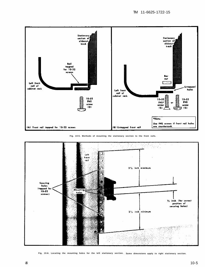
TM 11-6625-1722-15
Fig. 10-5. Methods of mounting the stationary section to the front rails.
Fig. 10-6. Locating the mounting holes for the left stationary section. Same dimensions apply to right stationary section.
10-5

TM 11-6625-1722-15
Fig. 10-7. Rear support kit.
Fig. 10-8. Installing the support black on the Instrument.
10-6

TM 11-6625-1722-15
Fig. 10-9. Procedure for inserting or removing the instrument after the slideout tracks have been installed.
10-7

TM 11-6625-l/22-15
Fig. 10-10. Alignment adjustments for correct operation.
Fig. 10-11. Alternative method of installing the instrument using rear support brackets.
10-8

Figure 10-12.
TM 11-6625-1722-15
Figure 10-13. Pivoting Dimensions.
10-9

FIG
UR
E 10-14.
10-10

TM 11-6625-1722-15
A P P E N D I X A
R E F E R E N C E S
DA Pam 310-4
DA Pam 310-7
SB 38-100
TB SIG 355-1TB SIG 355-2TB SIG 355-3
TB 43-0118
TB 43-180TM 11-6625-938-15
TM 11-6625-1549-15
TM 11-6625-1615-15
TM 11-6625-2376-15
TM 11-6625-2381-15
TM 11-6625-2383-15
TM 11-6625-2384-15
TM 11-6625-2385-15
TM 11-6625-2386-15
TM 11-6625-2399-15
TM 11-6625-2400-15
TM 38-750TM 740-90-1TM 750-244-2
Index of Technical Manuals, Technical Bulletins, Supply Manuals (Types7, 8, and 9), Supply Bulletins, and Lubrication Orders.
Military Publications: US Army Equipment Index of Modification WorkOrders.
Preservation, Packaging, Packing and Marking Materials, Supplies andEquipment Used by the Army.
Depot Inspection Standard for Repaired Signal Equipment.Depot Inspection Standard for Refinishing Repaired Signal Equipment.Depot Inspection Standard for Moisture and Fungus Resistant Treat-
ment.Field Instructions for Painting and Preserving Electronics Command
Equipment Including Camouflage Pattern Painting of ElectricalEquipment Shelters.
Calibration Requirements for the Maintenance of Army MaterielOperator, Organizational, Direct Support, General Support, and Depot
Maintenance Manual: Transportable Maintenance Calibration Facil-ity, AN/TSM-55A.
Operator’s, Organizational, Direct Support, General Support, and DepotMaintenance Manual: Test Set, Radio Frequency Power AN/USM-260.
Organizational, DS, GS, and Depot Maintenance Manual: Hewlett-Packard Oscilloscope Model 130C.
Operator’s, Organizational, DS, GS, and Depot Maintenance Manual,Including Repair Parts and Special Tools Lists: Signal GeneratorAN/USM-256.
Operator’s, Organizational, DS, GS, and Depot Maintenance Manual,Including Repair Parts and Special Tools Lists: Signal GeneratorAN/USM-269.
Operator’s, Organizational, DS, GS, and Depot Maintenance Manual:Electronic Marker Generator AN/USM-271.
Operator’s, Organizational, DS, GS, and Depot Maintenance Manual,Including Repair Parts and Special Tools Lists: Signal GeneratorAN/USM-272.
Operator’s, Organizational, Direct Support, General Support, and DepotMaintenance Manual: Multimeter, ME-333/U (NSN 6625-00-935-1425)and J-Omega Volt-Ohmmeter, Types 213A, 215A, and 219A.
Operator’s, Organizational, Direct Support, General Support, and DepotMaintenance Manual: Multimeter ME-338/U (NSN 6625-00-054-3486).
Operator’s, Organizational, Direct Support, General Support, and DepotMaintenance Manual (Including Repair Parts and Special Tool Lists):Electrical Meter Test Set, TS-2734/U.
Operator’s, Organizational, Direct Support, General Support, and DepotMaintenance Manual (Including Repair Parts and Special Tools Lists):Voltmeter TS-2843/U.
The Army Maintenance Management System (TAMMS).Administrative Storage of Equipment.Procedures for Destruction of Electronics Materiel to Prevent Enemy
Use (Electronics Command).
A-1


APPENDIX B
ITEMS COMPRISING AN OPERABLE EQUIPMENT
Oscilloscope AN/USM-273 Tektronix Model 4531 ea2 ea1 e a1 ea1 ea2 e a1 ea1 ea
Oscilloscope OS-188/U Major equipment less accessoriesAdapter, Connector UG-1825/U TEK 103-0033-00Adapter, Connector UG-1826/U TEK 012-0092-00Adapter, Connector UG-1867/U TEK 103-0013-00Cable Assembly, (SP) Electrical CX-10551/U TEK 161-0024-00Lead, Test CX-10552/U TEK 010-0188-00Cable Assembly, RF CG-3363/U TEK 012-0076-00Cover, Oscilloscope CU-931/U TEK 016-0074-01
The followlng additional items were furnished with the equipments supplied inTransportable Maintenance Calibration Facility AN/TSM-55 (V).
1 ea CRT Ring TEK 354-0269-001 ea Mesh Filter TEK 378-0573-001 ea Light Filter TEK 376-0576-001 ea CRT Protector Plate TEK 386-0218-002 ea Fuse, fast-blo, 2 amp, 3 A(3 TEK 159-0021-001 ea Fuse, fast-blo, 1 amp, 3 AG TEK 159-0022-001 ea Fuse, fast-blo, TEK 159-0025-001 ea Fuse, fast-blo, TEK 159-0026-00
B-1


TM 11-6625-1722-15
A P P E N D I X C
M A I N T E N A N C E A L L O C A T I O N
Section I . INTRODUCTION
C-1. General
This appendix provides a summary of the mainte-nance operations for Oscilloscope AN/USM-273(Tektronix 453). It authorizes categories of main-tenance for specific maintenance functions onrepairable items and components and the tools andequipment required to perform each function.Thisappendix may be used as an aid in planningmaintenance operations.
C-2. Maintenance Function
Maintenance functions will be limited to anddefined as follows:
a. Inspect. To determine the serviceability of anitem by comparing its physical, mechanical, and/orelectrical characteristics with established stand-ards through examination.
b. Test. To verify serviceability and to detectincipient failure by measuring the mechanical orelectrical characteristics of an item and comparingthose characteristics with prescribed standards.
c. Service. Operations required periodically tokeep an item in proper operating condition; i.e., toclean (decontaminate), to preserve, to drain, topaint, or to replenish fuel, lubricants, hydraulicfluids, or compressed air supplies.
d. Adjust. To maintain, within prescribed limits,by bringing into proper or exact position, or bysetting the operating characteristics to thespecified parameters.
e. Align. To adjust specified variable elements ofan item to bring about optimum or desiredperformance.
f. Calibrate. To determine and cause correctionsto be made or to be adjusted on instruments or testmeasuring and diagnostic equipments used inprecision measurement. Consists of comparisons oftwo instruments, one of which is a certifiedstandard of known accuracy, to detect and adjustany discrepancy in the accuracy of the instrumentbeing compared.
g. Install. The act of emplacing, seating, or fixinginto position an item, part, module (component orassembly) in a manner to allow the properfunctioning of the equipment or system.
h. Replace. The act of substituting a serviceablelike type part, subassembly, or module (componentor assembly) for an unserviceable counterpart.
i. Repair. The application of maintenance serv-
ices (inspect, test, service, adjust, align, calibrate,replace) or other maintenance actions (welding,grinding, riveting, straightening, facing, re-machining, or resurfacing) to restore serv-iceability to an item by correcting specific damage,fault, malfunction, or failure in a part, subassem-bly, module (component or assembly), end item, orsystem.
j. Overhaul. That maintenance effort (service/action) necessary to restore an item to a completelyserviceable/operational condition as prescribed bymaintenance standards (i.e., DMWR) in appropri-ate technical publications. Overhaul is normallythe highest degree of maintenance performed bythe Army. Overhaul does not normally return anitem to like new condition.
k. Rebuild. Consists of those services/actionsnecessary for the restoration of unserviceableequipment to a like new condition in accordancewith original manufacturing standards. Rebuild isthe highest degree of materiel maintenanceapplied to Army equipment. The rebuild operationincludes the act of returning to zero those agemeasurements (hours, miles, etc.) considered inclassifying Army equipments/components.
C-3. Column Entries
a. Column 1, Group Number. Column 1 listsgroup numbers, the purpose of which is to identifycomponents, assemblies, subassemblies, and mod-ules with the next higher assembly.
b. Column 2, Component/Assembly. Column 2contains the noun names of components, as-semblies, subassemblies, and modules for whichmaintenance is authorized.
c. Column 3, Maintenance Functions. Column 3lists the functions to be performed on the itemlisted in column 2. When items are listed withoutmaintenance functions, it is solely for purpose ofhaving the group numbers in the MAC and RPSTLcoincide.
d. Column 4, Maintenance Category. Column 4specifies, by the listing of a “work time” figure inthe appropriate subcolumn(s), the lowest level ofmaintenance authorized to perform the functionlisted in column 3. This figure represents the activetime required to perform that maintenance func-tion at the indicated category of maintenance. Ifthe number or complexity of the tasks within the
C-1

TM 11-6626-1722-15
listed maintenance function vary at differentmaintenance categories, appropriate “work time”figures will be shown for each category. Thenumber of task-hours specified by the “work time”figure represents the average time required torestore an item (assembly, subassembly, compo-nent, module, end item or system) to a serviceablecondition under typical field operating conditions.This time includes preparation time, trouble-shooting time, and quality assurance/quality con-trol time in addition to the time required toperform the specific tasks identified for themaintenance functions authorized in the mainte-nance allocation chart. Subcolumns of column 4are as follows:
C - Operator/CrewO - OrganizationalF - Direct SupportH - General SupportD - Depot
e. Column 5, Tools and Equipment. Column 5specifies by code, those common tool sets (notindividual tools) and special tools, test, and supportequipment required to perform the designatedfunction.
f. Column 6, Remarks. Column 6 contains analphabetic code which leads to the remark insection IV, Remarks, which is pertinent to the itemopposite the particular code.
C-4 Tool and Test Equipment Requirements(Sec III)
a. Tool or Test Equipment Reference Code. Thenumbers in this column coincide with the numbersused in the tools and equipment column of theMAC. The numbers indicate the applicable tool ortest equipment for the maintenance functions.
b. Maintenance Category. The codes in thiscolumn indicate the maintenance category allo-cated the tool or test equipment.
c. Nomenclature. This column lists the nounname and nomenclature of the tools and testequipment required to perform the maintenancefunctions.
d. National/NATO Stock Number. This columnlists the National/NATO stock number of thespecific tool or test equipment.
e. Tool Number. This column lists the manufac-turer’s part number of the tool followed by theFederal Supply Code for manufacturers (5-digit) inparentheses.
C-5. Remarks (Sec IV)
a. Reference Code. This code refers to theappropriate item in section II, column 6.
b. Remarks. This column provides the requiredexplanatory information necessary to clarify itemsappearing in section II.
(Next printed page is C-3)
C-2

03
02
01
0)GROUP
NUWER
00
TM 11-6625-1722-15
SECTION II MAINTENANCE ALLOCATION CHART
OSCILSLW
(2)COhlPONEIW/ASSEMBLY
OSCIL1OSCOPE AN/USN-Z73
CIRCUIT CARD AWEki8LV 670-0419-00 (80009)
PRINTEO 80ARD
PRINTEO BOARO
FOR
E AWUSM-273 (TEKTRONIX 453)SN 6625-00-930-6637)
(3)MAINTENANCE
FUNCTION
InspectTestTestAdjustInstallReplaceRepairOverhaul
TestReplace
TestReplace
TestRepl ace
(4)MA! NTENANCE C4TEGORY
c o
0.20.3
0.10.1
F H
1.01.0
2.0
0.40.3
0.40.3
0.40.3
D
4.0
(5)TOOL!3
ANDEQPT.
thru 1thru 1
6,176,17thru 1thru 1
thru 16,17
thru 16,17
thru 16,17
(6)REMARKS
AB
Change 1 C-3

TM 11-6625-1722-15
SECTION III TOOL AND TEST EQUIPMENT REQUIREMENTSFOR
OSCILLOSCOPE AN/USM-273 (TEKTRONIX 453)(NSN 6625-00-930-6637)
OOL OR TEST MAINTENANCEEQUIPMENT NOMENCLATURE
NATI ONA L/NATOCATEGORY
REF CODESTOCK NUMBER TOOL NUMBER
1 H,O TRANSFORMER, VARIABLE POWER TF-510/U (GR W1OMT3A) OR EQUAL 6120-00-054-7794
2 H,O GENERATOR, ELECTRONIC MARKER AN/usM-271 (TEKTRONIX 184) OR EQUAL 6625-00-982-1543
3 H.O TRANSFORMER, RAT[O oEcAoE TF-515u (S INGER-GERTSCH RT60) OR EquAL 5950-00-087-5433
4 H,O GENERATOR, SIGNAL AN/USM-272 (TEKTRONIX 191) OR EQUAL 6625-00-957-0421
5 H,o GENERATOR, SIGNAL AN/usM-269 (GR-1310A) 6625-00-054-3476
6 H,O COUNTER, ELECTRONIC REAOOUT AN/ USM-257A (SYSTEM 00NNER 1037) 6625-00-935-1457
7 H,O OSCILLOSCOPE AN/USM-254 (HP 130C) OR EQUAL 6625-00-069-5477
8 H,O MULTI METER ME-333/U OR EQUAL 6625-00-935-1425
9 H,O GENERATOR, SIGNAL AN/USM-264 (HP 652A) OR EQUAL 6625-00-935-4214
10 H,O TEST SET ELEcTRICAL METER TS-2734 (FLUKE 760A) OR EQUAL 6625-00-054-4976
11 H,D VOLTMETER TS-2843 (FLUKE 883AB OR 887AB) OR EQUAL 6625 -00-965 -B304
12 H,O GENERATOR, SIGNAL AN/usM-358 (TEKTRONt X 106) OR EQuAL 6625-00-455-7302
13 H,O CALIBRATOR, AMPLITUOE-COMPARATOR AN/USM-360 6625 -00-192 -0B66(TEKTRONIX 067-0502-01) OR EQUAL
14 H,o TEST SET, ELECTRON TU8E TV-70/U OR EQUAL 6625-00-820-0064
15 H,O TEST SET, TRANSISTOR TS-18360/U OR EQUAL 6625 -00-13 B-7320
16 O,H, O TOOL KIT, TK-100/G 5180-00-605-0079
17 O,H, O TOOLS AND TEST EQUIPMENT AVAILABLE TO THE REPAIRMAN IN HISASSIGNED MISSION.
C-4 Change 1

TM 11-6625-1722-15
REfERENCECOOE
A
B
SECTION IV. REMARKS
REMARKS
VISUAL INSPECTION
OPERATIONAL TEST
Change 1 C-5


TM 11-6625-1722-15
By Order of the Secretary of the Army:
Official:VERNE L. BOWERS,Major General, United States Army,The Adjutant General.
DISTRIBUTION:
Active Army
USASA (2)CNGB (1)ACSC-E (2)Dir of Trans (1)COE (1)TSG (1)CofSpts (1)USAARENBD (2)USAMB (10)USACDCCEA (1)USACDCCEA
Ft Huachuca (1)USACDC (1)USACDCOA (1)USAMC (1)CONARC (5)ARADCOM (2)ARADCOM Rgn (1)OS Maj Comd (4)LOGCOMD (2) except
1st Log Comd (5)9th Log Comd (5)
USAMICOM (5)USATECOM (2)USASTRATCOM (5)USASTRATCOM-SIG-GP-T (2 )USASTRATCOM-EUR (5)USASTRATCOM-PAC (5)USASTRATCOM-SO (5)USASTRATCOM-A (2)USARV (5)USAESC (40)MDW (1)Armies (2)Corps (2)1st Cav Div (2)Svc Colleges (2)
State AG (3)
USAR: None.
For explanation of abbreviations used see AR 310–50.
W. C. WESTMORELANDGeneral, United States Army,Chief of Staff.
USASCS (l0)USASESS (10)USAADS (2)USAINTS (3)USAFAS (2)USAARMS (2)USAIS (2)USAES (2)USAOC&S (2)USAMCC (3)Fort Huachuca (5)WSMR (3)Fort Carson (7)Army Dep (2) except
LBAD (14)SAAD (30)TOAD (14)LEAD (7)ATAD (10)
USACDCEC (10)Gen Dep (2)Sig Sec Gen Dep (5)Sig Dep (5)USACRREL (2)WRAMC (1)Sig FLDMS (1)ATS (1)USAERDAA (2)USAERDAW (5)Units org under fol TOE:
(2 cys each unit)9 - 5 5 01 1 - 1 5 82 9 - 1 3 42 9 - 2 2 72 9 - 6 7 0
, U.S. GOVERNMENT ~! NTINQ OFFICE: 1981 -347-092


FIG. FO-1 FRONT TM 11-6625-1722-15

FIG. FO-2 ATTENUATOR PREAMPLIFIER ASSEMBLYTM 11-6625-1722-15
TYPE 453/R453 OSCILLOSCOPE

FIG. FO-3 CRT SHIELDTM 11-6625-1722-15
TYPE 453/R453 OSCILLOSCOPE

TM 11-6625-1722-15
FIG. FO-5 HIGH VOLTAGE ASSEMBLY
TYPE 453/R453 OSCILLOSCOPE

TM 11-6625-1722-15
FIG. FO-6 REAR CHASSIS
TYPE 453/R453 OSCILLOSCOPE

TM 11-6625-1722-15
FIG. FO-7 FRAME & CABINET
TYPE 453/R453 OSCILLOSCOPE

FIG. FO-8 R453 MECHANICAL PARTS TM 11-6625-1722-15
TYPE 453/R453 OSCILLOSCOPE


TM 11-6625-1722-15
VOLTAGE AND WAVEFORMTEST CONDTIONS
Typical voltage measurements and waveform photographswore obtained under the following conditions unless notedotherwise on the individual diagram:
Test Oscilloscope (With 10 Probe)
Vertical Controls (both channels if applicable)
VOLTS/DIV 20 mV
VARIABLE CAL
POSITION Midrange
Input Coupling DC
MODE CH 1
TRIGGER NORM
INVERT Pushed in
Triggering Controls (both A and B If applicable)
Frequency response
Deflection factor(with probe)
Input impedance
Dc to 20 MHz
50 millivolts to 10 volts/division
10 Megohms, 735 pico-farads
Type 453 chassis ground
External from A GATEconnector to indicatetrue time relationshipbetween signals
Tektronix Type 545B withType 1A1 plug-in unit
Probe ground
Trigger Source
LEVEL
SLOPE
COUPLING
SOURCE
Sweep Controls
DELAY-TIME MULTIPLIER
A TIME/DIV
B TIME/DIV
A VARIABLE
A SWEEP MODE
B SWEEP MODE
HORIZ DISPLAY
MAG
A SWEEP LENGTH
POSITION
FINE
POWER
Side-PaneI Controls
B TIME/DIV VARIABLE
CALIBRATOR
0
+
AC
INT
Recommended type(as used for waveformson diagrams)
Veltmeter
Type 0.20
1 ms
1 ms
CAL
AUTO TRIG
TRIGGERABLE AFTERDELAY TIME
A
OFF
FULL
Midrange
Non-loading AC (RMS)-DC VTVM
20,000 ohms/volt
0 to 300 volts
Type 452 chassis ground
General Radio Type 1806-A Electronic Voltmeter
Sensitivity
Range
Reference voltage
Recommended type(as used for voltageson diagrams)
Type 453 Conditions
Line voltage
Signal applied115 volts
Calibrator output signalconnected to Channel1 and 2 INPUT con-nectors for waveforms O NOnly
No connections(except as above)
Centered
AS fallows except asnoted otherwise ondividual diagrams:
Midrange
Trace position
Control settings
CAL
1 Vin-
All voltages given on the diagrams are in volts. Waveformsshown are actual waveform photographs taken with a Tek-tronix Oscilloscope Camera System and Projected Graticule.Voltages and waveforms on the diagrams (shown in blue)are not absolute and may vary between instruments becauseof differing component tolerances, internal calibration orfront-panel control settings.
CRT Controls
INTENSITY
FOCUS
SCALE ILLUMAdjust for focused display
AS desired T Y P E 4 5 3 O S C I L L O S C O P E FIG. FO-11. CHANNEL 1 VERTICAL PREAMP

TM 11-6625-1722-15
TYPE 453 OSCILLOSCOPEFIG. FO-12 CHANNEL 1 ATTENUATORS

TM 11-6625-1722-15
FIG. FO-13 CHANNEL 2 VERTICAL PREAMPTYPE 453 OSCILLOSCOPE

FIG. FO-14
TM 11-6625-1722-15

FIG. FO-15
TM 11-6625-1722-15

TM 11-6625-1722-15
FIG. FO-16 VERTICAL OUTPUT AMPLIFIER

FIG. FO-17
TM 11-6625-1722-15

TM 11-6625-1722-15
FIG. FO-18 A TRIGGER GENERATORTYPE 453 OSCILLOSCOPE

FIG. FO-19
TM 11-6625-1722-15

TM 11-6625-1722-15
FIG. FO-20
B TRIGGER GENERATOR

FIG. FO-21
TM 11-6625-1722-15

FIG. FO-22
TM 11-6625-1722-15

FIG. FO-23
TM 11-6625-1722-15

FIG. FO-24
TM 11-6625-1722-15

FIG. FO-25
TM 11-6625-1722-15

FIG. FO-26
TM 11-6625-1722-15

TM 11-6625-1722-15
TYPE 453 OSCILLOSCOPE FIG. FO-27.

FIG. FO-28.
TM 11-6625-1722-15
TYPE 453 OSCILLOSCOPE


This fine document...
Was brought to you by me:
Liberated Manuals -- free army and government manuals
Why do I do it? I am tired of sleazy CD-ROM sellers, who take publicly available information, slap “watermarks” and other junk on it, and sell it. Those masters of search engine manipulation make sure that their sites that sell free information, come up first in search engines. They did not create it... They did not even scan it... Why should they get your money? Why are not letting you give those free manuals to your friends?
I am setting this document FREE. This document was made by the US Government and is NOT protected by Copyright. Feel free to share, republish, sell and so on.
I am not asking you for donations, fees or handouts. If you can, please provide a link to liberatedmanuals.com, so that free manuals come up first in search engines:
<A HREF=http://www.liberatedmanuals.com/>Free Military and Government Manuals</A>
– SincerelyIgor Chudovhttp://igor.chudov.com/
– Chicago Machinery Movers