Operation of SOI P-Channel Field Effect Transistors, CHT ...
6
June 2009 NASA Electronic Parts and Packaging Program Operation of SOI P-Channel Field Effect Transistors, CHT-PMOS30, under Extreme Temperatures Richard Patterson, NASA Glenn Research Center Ahmad Hammoud, ASRC Aerospace / NASA GRC Scope Electronic systems are required to operate under extreme temperatures in NASA planetary exploration and deep space missions. Electronics on-board spacecraft must also tolerate thermal cycling between extreme temperatures. Thermal management means are usually included in today’s spacecraft systems to provide adequate temperature for proper operation of the electronics. These measures, which may include heating elements, heat pipes, radiators, etc., however add to the complexity in the design of the system, increases its cost and weight, and affects its performance and reliability. Electronic parts and circuits capable of withstanding and operating under extreme temperatures would reflect in improvement in system’s efficiency, reducing cost, and improving overall reliability. Semiconductor chips based on silicon-on-insulator (SOI) technology are designed mainly for high temperature applications and find extensive use in terrestrial well-logging fields. Their inherent design offers advantages over silicon devices in terms of reduced leakage currents, less power consumption, faster switching speeds, and good radiation tolerance. Little is known, however, about their performance at cryogenic temperatures and under wide thermal swings. Experimental investigation on the operation of SOI, N-channel field effect transistors under wide temperature range was reported earlier [1]. This work examines the performance of P-channel devices of these SOI transistors. The electronic part investigated in this work comprised of a Cissoid’s CHT-PMOS30, high temperature P-channel MOSFET (metal-oxide semiconductor field-effect transistor) device [2]. This high voltage, medium-power transistor is designed for geothermal well logging applications, aerospace and avionics, and automotive industry, and is specified for operation in the temperature range of -55 °C to +225 °C. Table I shows some specifications of this transistor [2]. The CHT-PMOS30 device was characterized at various temperatures over the range of -190 °C to +225 °C in terms of its voltage/current characteristic curves. The test temperatures included +22, -50, -100, -150, -175, -190, +50, +100, +150, +175, +200, and +225 °C. Limited thermal cycling testing was also performed on the device. These tests consisted of subjecting the transistor to a total of twelve thermal cycles between -190 °C and +225 °C. A temperature rate of change of 10 °C/min and a soak time at the test temperature of 10 minutes were used throughout this work. Post-cycling measurements were also performed at selected temperatures. In addition, re-start capability at extreme temperatures, i.e. power switched on while the device was soaking for a period of 20 minutes at the test temperatures of -190 °C and +225 °C, was investigated.
Transcript of Operation of SOI P-Channel Field Effect Transistors, CHT ...

June 2009 NASA Electronic Parts and Packaging Program
Operation of SOI P-Channel Field Effect Transistors, CHT-PMOS30, under
Extreme Temperatures
Richard Patterson, NASA Glenn Research Center Ahmad Hammoud, ASRC Aerospace / NASA GRC
Scope Electronic systems are required to operate under extreme temperatures in NASA planetary exploration and deep space missions. Electronics on-board spacecraft must also tolerate thermal cycling between extreme temperatures. Thermal management means are usually included in today’s spacecraft systems to provide adequate temperature for proper operation of the electronics. These measures, which may include heating elements, heat pipes, radiators, etc., however add to the complexity in the design of the system, increases its cost and weight, and affects its performance and reliability. Electronic parts and circuits capable of withstanding and operating under extreme temperatures would reflect in improvement in system’s efficiency, reducing cost, and improving overall reliability. Semiconductor chips based on silicon-on-insulator (SOI) technology are designed mainly for high temperature applications and find extensive use in terrestrial well-logging fields. Their inherent design offers advantages over silicon devices in terms of reduced leakage currents, less power consumption, faster switching speeds, and good radiation tolerance. Little is known, however, about their performance at cryogenic temperatures and under wide thermal swings. Experimental investigation on the operation of SOI, N-channel field effect transistors under wide temperature range was reported earlier [1]. This work examines the performance of P-channel devices of these SOI transistors. The electronic part investigated in this work comprised of a Cissoid’s CHT-PMOS30, high temperature P-channel MOSFET (metal-oxide semiconductor field-effect transistor) device [2]. This high voltage, medium-power transistor is designed for geothermal well logging applications, aerospace and avionics, and automotive industry, and is specified for operation in the temperature range of -55 °C to +225 °C. Table I shows some specifications of this transistor [2]. The CHT-PMOS30 device was characterized at various temperatures over the range of -190 °C to +225 °C in terms of its voltage/current characteristic curves. The test temperatures included +22, -50, -100, -150, -175, -190, +50, +100, +150, +175, +200, and +225 °C. Limited thermal cycling testing was also performed on the device. These tests consisted of subjecting the transistor to a total of twelve thermal cycles between -190 °C and +225 °C. A temperature rate of change of 10 °C/min and a soak time at the test temperature of 10 minutes were used throughout this work. Post-cycling measurements were also performed at selected temperatures. In addition, re-start capability at extreme temperatures, i.e. power switched on while the device was soaking for a period of 20 minutes at the test temperatures of -190 °C and +225 °C, was investigated.

Table I. Manufacturer’s specifications of CHT-PMOS30 transistor [2].
Parameter Rating Units Operating temperature, T –55 to +225 °C Drain current, ID 1.9 to 2.8 A Drain-source breakdown voltage, VDS(BR) > -30 V Drain-source on-state resistance, RDS(on) at VGS= -5V & VDS= -50mV 1.7 to 3.9 Ω Gate threshold voltage, VGS(th) @ VDS = -50mV -0.8 to3-1.4 V Gate-source voltage, VGS -6 to 1 V Package TO3 Lot Number 2080162.1
Results and Discussion Although two devices of this CHT-PMOS30 transistor were evaluated in this work, data pertaining to only one is presented due to the similarity in the results of both devices. Temperature Effects The pre-cycling drain current (ID) versus drain-to-source voltage (VDS) curves at various gate voltages (VGS) of the SOI CHT-PMOS30 transistor at selected test temperatures between -190 °C and +225 °C are shown in Figure 1. In the temperature regime between +22 °C and -190 °C, the transistor’s linear region initially decreased, as reflected by the increase in the slope of its ID/VDS curves, with decreasing temperature down to -100 °C; but it reversed trend as the test temperature was reduced further. This initial increase in the slope of the curves with decreasing temperature to -100 °C is an indication of a decrease in the transistor drain-to-source on-state resistance RDS(on). At -150 °C and cooler temperatures, however, the on-state resistance exhibited an increase with further decrease in temperature, as shown in Figure 1. In the other temperature region, i.e. high temperatures, the SOI transistor exhibited a gradual, slight increase in its drain-to-source on-state resistance RDS(on) as the temperature was increased from +22 °C to +225 °C. Figure 1 also shows that the gate threshold voltage (VGS(th)) of the SOI transistor exhibited gradual decrease as the test temperature was swept from -190 °C to +225 °C. These temperature-induced changes in the characteristics of the device could be attributed to redistribution in the dopants in the P-channel of the transistor and possible diffusion into the oxide gate, and to surface potentials that are created by interface and mobile ionic charges created by the thermal stress, especially at high temperatures. Re-Start at Extreme Temperatures Re-start capability of the P-channel SOI PMOS30 transistor was investigated by allowing it to soak at each of the extreme test temperatures for at least 20 minutes without the application of electrical bias. Power was then applied to the device and measurements were taken on the output characteristics. The SOI transistor was able to successfully re-start at either extreme, i.e. -190 °C and +225 °C, and the results obtained were the same as those obtained earlier at each corresponding temperature.

VDS , Drain-Source Voltage (V)
-0 -1 -2 -3 -4 -5
ID, D
rain
Cu
rren
t (A
)
-0.0
-0.1
-0.2
-0.3
-0.4
-0.5
VGS = -3 V
-2.2 V
-2 V
-1.8 V
-1.6 V
-1.4 V
-2.4 V
(+22 °C)
VDS , Drain-Source Voltage (V)
-0 -1 -2 -3 -4 -5
ID, D
rain
Cur
rent
(A
)
-0.0
-0.1
-0.2
-0.3
-0.4
-0.5
VGS = -3 V
-1.8 V
-1.6 V
-1.4 V
-1.2 V
(-175 °C)
VDS , Drain-Source Voltage (V)
-0 -1 -2 -3 -4 -5
I D, D
rain
Cur
rent
(A
)
-0.0
-0.1
-0.2
-0.3
-0.4
-0.5
VGS = -3 V
-2 V
-1.8 V
-1.6 V-1.4 V
-1.2 V
-2.2 V
(+175 °C)
VDS , Drain-Source Voltage (V)
-0 -1 -2 -3 -4 -5
I D, D
rain
Cu
rren
t (A
)
-0.0
-0.1
-0.2
-0.3
-0.4
-0.5VGS = -3 V
-2 V
-1.8 V
-1.6 V
-1.4 V
(-100 °C)
VDS , Drain-Source Voltage (V)
-0 -1 -2 -3 -4 -5
ID, D
rain
Cur
rent
(A
)
-0.0
-0.1
-0.2
-0.3
-0.4
-0.5
VGS = -3 V-1.8 V
-1.6 V
-1.4 V
-1.2 V
(-190 °C)
VDS , Drain-Source Voltage (V)
-0 -1 -2 -3 -4 -5
ID, D
rain
Cur
rent
(A
)
-0.0
-0.1
-0.2
-0.3
-0.4
-0.5
VGS = -3 V
-2 V
-1.8 V
-1.6 V
-1.4 V-1.2 V
-2.2 V
(+200 °C)
VDS , Drain-Source Voltage (V)
-0 -1 -2 -3 -4 -5
ID, D
rain
Cur
rent
(A
)
-0.0
-0.1
-0.2
-0.3
-0.4
-0.5
VGS = -3 V
-1.8 V
-1.6 V
-1.4 V
-1.2 V
(-150 °C)
VDS , Drain-Source Voltage (V)
-0 -1 -2 -3 -4 -5
ID, D
rain
Cur
rent
(A
)
-0.0
-0.1
-0.2
-0.3
-0.4
-0.5
VGS = -3 V
-2 V
-1.8 V
-1.6 V
-1.4 V
-1.2 V
-2.2 V
(+150 °C)
VDS , Drain-Source Voltage (V)
-0 -1 -2 -3 -4 -5
ID, D
rain
Cur
rent
(A
)
-0.0
-0.1
-0.2
-0.3
-0.4
-0.5
VGS = -3 V
-2 V
-1.8 V
-1.6 V-1.4 V
-1.2 V
-2.2 V
(+225 °C)
Figure 1. Pre-cycling characteristics of the CHT-PMOS30 transistor at various test temperatures.

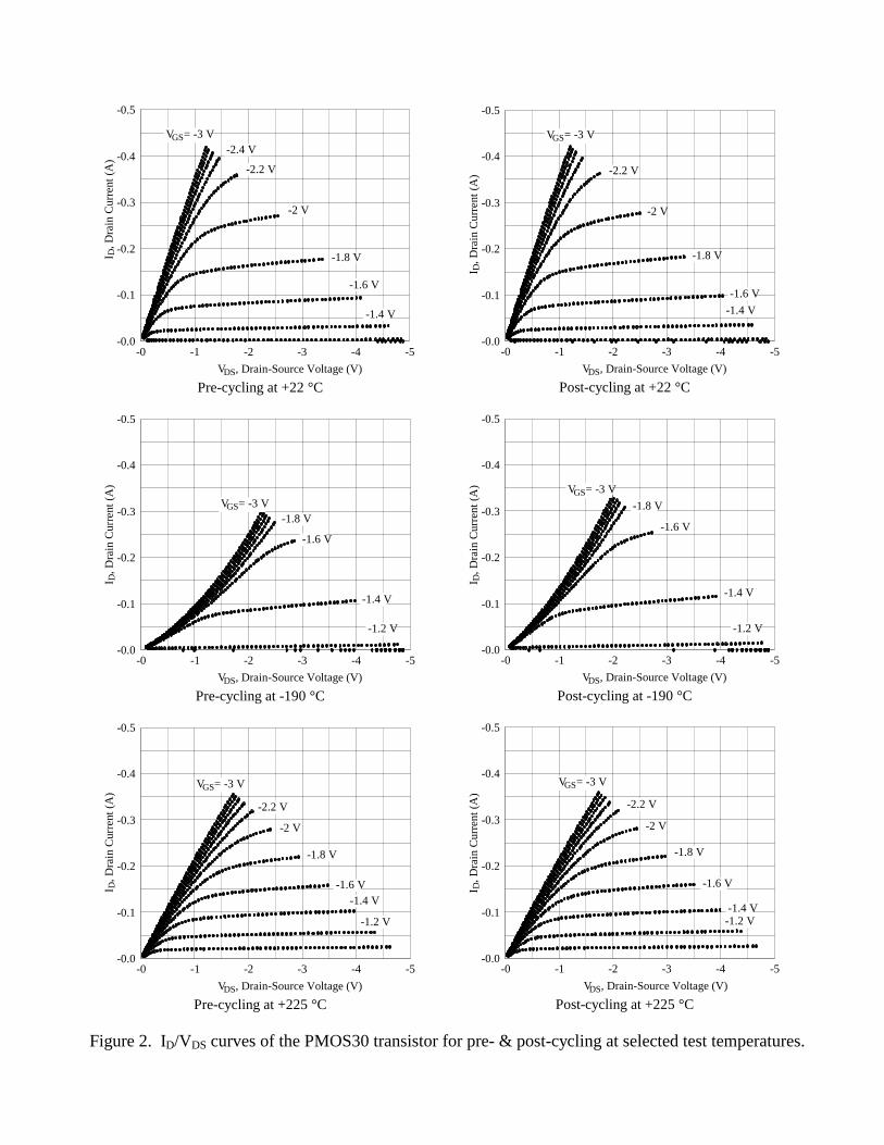
Effects of Thermal Cycling The effects of thermal cycling under a wide temperature range on the operation of the PMOS30 transistor were investigated by subjecting the device to a limited thermal cycling consisting of 12 cycles between -190 °C and +225 °C at a temperature rate of 10 °C/min and a soak time at the extreme temperatures of at least 10 minutes. ID versus VDS curves at various gate voltages (VGS) were then taken at +22 °C, -190 °C, and +225 °C. Comparison of the output characteristics of the SOI transistor at these selected test temperatures before and after the thermal cycling are depicted in Figure 2. It can be seen that the PMOS30 transistor did not display any significant change in its characteristics. In addition, the device did not experience any package deterioration or structural damage due to the extreme temperature exposure and thermal cycling.
Conclusion New P-channel SOI transistors were evaluated in the wide temperature range of -190 °C to +225 °C for potential use at extreme temperatures. The mid power prototype CHT-PMOS30 devices, were recently introduced by Cissoid Corporation for use in power switching and motor control applications under high temperature conditions such as in well logging fields. Drain current (ID) versus drain-to-source voltage (VDS) characteristics of the MOSFET device were obtained at various temperatures. Re-start at extreme temperatures and the effect of thermal cycling on the operation of the transistor were also investigated. The SOI MOSFET device was able to maintain good operation throughout the test temperature range of +225 °C to -150 °C. At lower temperatures, i.e. -175 °C to -190 °C, the transistor continued to operate but its ID/VDS curves exhibited some deviation in their characteristics. These changes comprised of an increase in the on-state resistance RDS(on), an increase in the gate threshold voltage (VGS(th)), and a reduction in drain current level that can be achieved at other test temperature for a given bias conditions. The changes, however, were temporary as the device recovers to its original characteristics upon removal of the thermal stress. The SOI transistor was able to re-start at the extreme temperatures of -190 °C and +225 °C, and the applied limited thermal cycling has yielded no effect on its performance or on its packaging. These preliminary results suggest that the CHT-PMOS30 transistor could potentially be used under wide temperature conditions but further comprehensive testing is required to establish its reliability for long term application in extreme temperature space exploration missions. References [1]. “SOI N-Channel Field Effect Transistors, CHT-NMOS89, for Extreme Temperatures”,
NASA Report, February 2009, www.nepp.nasa.gov. [2]. Cissoid Company, “CHT-PMOS30 High Temperature, P-Channel Mid-Power Transistor”
Data Sheet, Version: 04.00, May 9, 2008.
VDS , Drain-Source Voltage (V)
-0 -1 -2 -3 -4 -5
ID
, D
rain
Cur
rent
(A
)
-0.0
-0.1
-0.2
-0.3
-0.4
-0.5
VGS = -3 V
-2.2 V
-2 V
-1.8 V
-1.6 V
-1.4 V
-2.4 V
Pre-cycling at +22 °C
VDS , Drain-Source Voltage (V)
-0 -1 -2 -3 -4 -5
ID
, D
rain
Cur
rent
(A
)
-0.0
-0.1
-0.2
-0.3
-0.4
-0.5
VGS = -3 V-1.8 V
-1.6 V
-1.4 V
-1.2 V
Pre-cycling at -190 °C
VDS , Drain-Source Voltage (V)
-0 -1 -2 -3 -4 -5
ID
, D
rain
Cur
rent
(A
)
-0.0
-0.1
-0.2
-0.3
-0.4
-0.5
VGS = -3 V
-2 V
-1.8 V
-1.6 V-1.4 V
-1.2 V
-2.2 V
Pre-cycling at +225 °C
VDS , Drain-Source Voltage (V)
-0 -1 -2 -3 -4 -5
I D,
Dra
in C
urre
nt (
A)
-0.0
-0.1
-0.2
-0.3
-0.4
-0.5
VGS = -3 V
-2.2 V
-2 V
-1.8 V
-1.6 V
-1.4 V
Post-cycling at +22 °C
VDS , Drain-Source Voltage (V)
-0 -1 -2 -3 -4 -5
I D,
Dra
in C
urre
nt (
A)
-0.0
-0.1
-0.2
-0.3
-0.4
-0.5
VGS = -3 V
-1.8 V
-1.6 V
-1.4 V
-1.2 V
Post-cycling at -190 °C
VDS , Drain-Source Voltage (V)
-0 -1 -2 -3 -4 -5
ID
, D
rain
Cur
rent
(A
)
-0.0
-0.1
-0.2
-0.3
-0.4
-0.5
VGS = -3 V
-2 V
-1.8 V
-1.6 V
-1.4 V-1.2 V
-2.2 V
Post-cycling at +225 °C
Figure 2. ID/VDS curves of the PMOS30 transistor for pre- & post-cycling at selected test temperatures.

Acknowledgments This work was performed under the NASA Glenn Research Center GESS-2 Contract # NNC06BA07B. Funding was provided by the NASA Electronic Parts and Packaging (NEPP) Program.