Open-Access Silicon Photonics: Current Status and Emerging ...
18
Open-Access Silicon Photonics: Current Status and Emerging Initiatives Silicon photonic devices are usually fabricated in large foundries that serve multiple customers. Silicon photonics takes advantage of these open-access silicon electronics foundries. This paper discusses this ecosystem and its evolution. ABDUL RAHIM ,THIJS SPUESENS, Member IEEE,ROEL BAETS , Fellow IEEE, AND WIM BOGAERTS, Senior Member IEEE ABSTRACT | Silicon photonics is widely acknowledged as a game-changing technology driven by the needs of datacom and telecom. Silicon photonics builds on highly capital-intensive manufacturing infrastructure, and mature open-access silicon photonics platforms are translating the technology from research fabs to industrial manufacturing lev- els. To meet the current market demands for silicon photonics manufacturing, a variety of open-access platforms is offered by CMOS pilot lines, R&D institutes, and commercial foundries. This paper presents an overview of existing and upcoming commercial and noncommercial open-access silicon photonics technology platforms. We also discuss the diversity in these open-access platforms and their key differentiators. KEYWORDS | CMOS; foundry; multiproject wafer (MPW); open- access; photonic integrated circuits (PICs); photonic manufac- turing; silicon photonics. I. INTRODUCTION Silicon photonics is a technology which implements high-density photonic integrated circuits (PICs) with complex functionality using process technology of a complementary metal–oxide–semiconductor (CMOS) elec- tronics fab. Leveraging the existing CMOS infrastruc- ture makes silicon photonics very well positioned to Manuscript received May 23, 2018; revised October 6, 2018 and October 26, 2018; accepted October 27, 2018. Date of current version November 20, 2018. (Corresponding author: Abdul Rahim.) The authors are with the Photonics Research Group, Department of Information Technology, Ghent University/imec, B-9052 Ghent, Belgium, and also with the Center for Nano- and Biophotonics, Ghent University, B-9052 Ghent, Belgium (e-mail: [email protected]; [email protected]; [email protected]; [email protected]). Digital Object Identifier 10.1109/JPROC.2018.2878686 fabricate low cost, high yield, small form-factor, and low-power PICs and, at the same time, scale to large commercial volumes [1]–[3]. The above-mentioned defi- nition of silicon photonics holds for a variety of mate- rial systems. To name a few, this includes different types of silicon-on-insulator (SOI), silicon nitride-on- insulator (SiN), germanium-on-insulator, germanium-on- silicon (GOS), germanium-on-SOI, GOS nitride, and silicon-on-silicon nitride-on-silicon. Since all these mate- rial systems can use well-established CMOS processing methodologies and infrastructure for densely integrated PICs, they can be considered as different flavors of silicon photonics, but to date the SOI platform has been the most prominent of these material systems both in terms of technological maturity and commercial use. The last decade has seen the transformation of silicon photonics from a promising research field to a commercial success, mainly driven by the needs for large volumes of high-speed links for datacenters, metro communica- tion, and telecommunication. However, the first conceived applications of silicon photonics were for sensing applica- tions, such as fiber gyroscopes [4]. Nevertheless, variable optical attenuators (VOAs) for passive optical networks (PONs), developed and commercialized by Bookham Technologies in 1997 (with the technology later taken up by Kotura and afterward by Mellanox), were one of the first silicon photonics products to be actually commercialized [4]. Building up to the dot-com boom (and subsequent bust) in the early 2000s, silicon photonics was being considered as a technology that could address the demands of emerging tele/data communication appli- cations. The bursting of the dot-com bubble did little to reduce that expectation but had an obvious negative effect on the investment climate for silicon photonics. It is only 0018-9219 © 2018 IEEE. Personal use is permitted, but republication/redistribution requires IEEE permission. See http://www.ieee.org/publications_standards/publications/rights/index.html for more information. Vol. 106, No. 12, December 2018 |PROCEEDINGS OF THE IEEE 2313
Transcript of Open-Access Silicon Photonics: Current Status and Emerging ...

Open-Access SiliconPhotonics: Current Statusand Emerging InitiativesSilicon photonic devices are usually fabricated in large foundries that serve multiplecustomers. Silicon photonics takes advantage of these open-access silicon electronicsfoundries. This paper discusses this ecosystem and its evolution.
ABDUL RAHIM , THIJS SPUESENS, Member IEEE, ROEL BAETS , Fellow IEEE,AND WIM BOGAERTS, Senior Member IEEE
ABSTRACT | Silicon photonics is widely acknowledged
as a game-changing technology driven by the needs of
datacom and telecom. Silicon photonics builds on highly
capital-intensive manufacturing infrastructure, and mature
open-access silicon photonics platforms are translating the
technology from research fabs to industrial manufacturing lev-
els. To meet the current market demands for silicon photonics
manufacturing, a variety of open-access platforms is offered
by CMOS pilot lines, R&D institutes, and commercial foundries.
This paper presents an overview of existing and upcoming
commercial and noncommercial open-access silicon photonics
technology platforms. We also discuss the diversity in these
open-access platforms and their key differentiators.
KEYWORDS | CMOS; foundry; multiproject wafer (MPW); open-
access; photonic integrated circuits (PICs); photonic manufac-
turing; silicon photonics.
I. I N T R O D U C T I O N
Silicon photonics is a technology which implementshigh-density photonic integrated circuits (PICs) withcomplex functionality using process technology of acomplementary metal–oxide–semiconductor (CMOS) elec-tronics fab. Leveraging the existing CMOS infrastruc-ture makes silicon photonics very well positioned to
Manuscript received May 23, 2018; revised October 6, 2018 and October 26,2018; accepted October 27, 2018. Date of current version November 20, 2018.(Corresponding author: Abdul Rahim.)
The authors are with the Photonics Research Group, Department of InformationTechnology, Ghent University/imec, B-9052 Ghent, Belgium, and also with theCenter for Nano- and Biophotonics, Ghent University, B-9052 Ghent, Belgium(e-mail: [email protected]; [email protected]; [email protected];[email protected]).
Digital Object Identifier 10.1109/JPROC.2018.2878686
fabricate low cost, high yield, small form-factor, andlow-power PICs and, at the same time, scale to largecommercial volumes [1]–[3]. The above-mentioned defi-nition of silicon photonics holds for a variety of mate-rial systems. To name a few, this includes differenttypes of silicon-on-insulator (SOI), silicon nitride-on-insulator (SiN), germanium-on-insulator, germanium-on-silicon (GOS), germanium-on-SOI, GOS nitride, andsilicon-on-silicon nitride-on-silicon. Since all these mate-rial systems can use well-established CMOS processingmethodologies and infrastructure for densely integratedPICs, they can be considered as different flavors of siliconphotonics, but to date the SOI platform has been themost prominent of these material systems both in termsof technological maturity and commercial use.
The last decade has seen the transformation of siliconphotonics from a promising research field to a commercialsuccess, mainly driven by the needs for large volumesof high-speed links for datacenters, metro communica-tion, and telecommunication. However, the first conceivedapplications of silicon photonics were for sensing applica-tions, such as fiber gyroscopes [4]. Nevertheless, variableoptical attenuators (VOAs) for passive optical networks(PONs), developed and commercialized by BookhamTechnologies in 1997 (with the technology later takenup by Kotura and afterward by Mellanox), were oneof the first silicon photonics products to be actuallycommercialized [4]. Building up to the dot-com boom(and subsequent bust) in the early 2000s, silicon photonicswas being considered as a technology that could addressthe demands of emerging tele/data communication appli-cations. The bursting of the dot-com bubble did little toreduce that expectation but had an obvious negative effecton the investment climate for silicon photonics. It is only
0018-9219 © 2018 IEEE. Personal use is permitted, but republication/redistribution requires IEEE permission.See http://www.ieee.org/publications_standards/publications/rights/index.html for more information.
Vol. 106, No. 12, December 2018 | PROCEEDINGS OF THE IEEE 2313
Rahim et al.: Open-Access Silicon Photonics: Current Status and Emerging Initiatives
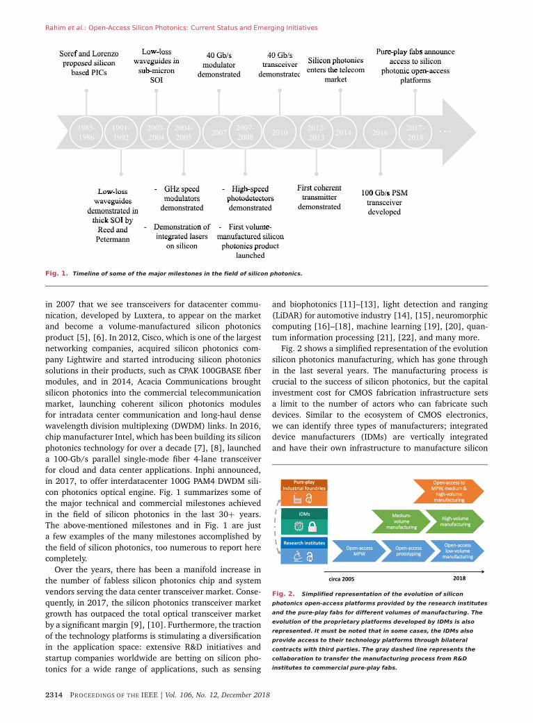
Fig. 1. Timeline of some of the major milestones in the field of silicon photonics.
in 2007 that we see transceivers for datacenter commu-nication, developed by Luxtera, to appear on the marketand become a volume-manufactured silicon photonicsproduct [5], [6]. In 2012, Cisco, which is one of the largestnetworking companies, acquired silicon photonics com-pany Lightwire and started introducing silicon photonicssolutions in their products, such as CPAK 100GBASE fibermodules, and in 2014, Acacia Communications broughtsilicon photonics into the commercial telecommunicationmarket, launching coherent silicon photonics modulesfor intradata center communication and long-haul densewavelength division multiplexing (DWDM) links. In 2016,chip manufacturer Intel, which has been building its siliconphotonics technology for over a decade [7], [8], launcheda 100-Gb/s parallel single-mode fiber 4-lane transceiverfor cloud and data center applications. Inphi announced,in 2017, to offer interdatacenter 100G PAM4 DWDM sili-con photonics optical engine. Fig. 1 summarizes some ofthe major technical and commercial milestones achievedin the field of silicon photonics in the last 30+ years.The above-mentioned milestones and in Fig. 1 are justa few examples of the many milestones accomplished bythe field of silicon photonics, too numerous to report herecompletely.
Over the years, there has been a manifold increase inthe number of fabless silicon photonics chip and systemvendors serving the data center transceiver market. Conse-quently, in 2017, the silicon photonics transceiver marketgrowth has outpaced the total optical transceiver marketby a significant margin [9], [10]. Furthermore, the tractionof the technology platforms is stimulating a diversificationin the application space: extensive R&D initiatives andstartup companies worldwide are betting on silicon pho-tonics for a wide range of applications, such as sensing
and biophotonics [11]–[13], light detection and ranging(LiDAR) for automotive industry [14], [15], neuromorphiccomputing [16]–[18], machine learning [19], [20], quan-tum information processing [21], [22], and many more.
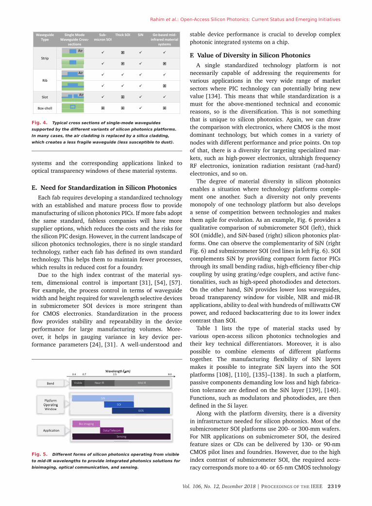
Fig. 2 shows a simplified representation of the evolutionsilicon photonics manufacturing, which has gone throughin the last several years. The manufacturing process iscrucial to the success of silicon photonics, but the capitalinvestment cost for CMOS fabrication infrastructure setsa limit to the number of actors who can fabricate suchdevices. Similar to the ecosystem of CMOS electronics,we can identify three types of manufacturers; integrateddevice manufacturers (IDMs) are vertically integratedand have their own infrastructure to manufacture silicon
Fig. 2. Simplified representation of the evolution of silicon
photonics open-access platforms provided by the research institutes
and the pure-play fabs for different volumes of manufacturing. The
evolution of the proprietary platforms developed by IDMs is also
represented. It must be noted that in some cases, the IDMs also
provide access to their technology platforms through bilateral
contracts with third parties. The gray dashed line represents the
collaboration to transfer the manufacturing process from R&D
institutes to commercial pure-play fabs.
2314 PROCEEDINGS OF THE IEEE | Vol. 106, No. 12, December 2018

Rahim et al.: Open-Access Silicon Photonics: Current Status and Emerging Initiatives
photonics chips for their own products. In stark con-trast, pure-play foundries have an open-access manufac-turing process, where the fabs offer PIC manufacturingservices that can be used hands-off by third party externalusers/clients, such as fabless companies. The notion “open-access” does not mean that the manufacturing servicesare free of cost to the end users, but rather that thefab imposes little or no restrictions to fabricate PICs forthird parties. This is contrary to other areas of com-merce, where open access implies that there is no costto the end users (for example, open-access publications).Anticipating a growing demand for silicon photonics PICmanufacturing, such pure-play foundries [Advanced MicroFoundry (AMF), GlobalFoundries, TowerJazz, and others]have emerged in recent years to offer open-access siliconphotonics technologies [23] to cater various manufactur-ing volumes. The third type of manufacturer is the CMOSpilot line at an advanced (public or private) researchinstitute [24]–[32]. They offer open access to their plat-forms, which includes multiproject wafer (MPW) fabrica-tion, and this has allowed these institutes to continuouslyimprove their technology offering, to a point where thehigh technology readiness level (TRL) of their platformshas enabled them to offer low-volume manufacturing ofsilicon photonic chips through bilateral contracts. In somecases, the R&D institute/pilot line uses the same processflow as a commercial fab to ease the transfer of manu-facturing process from R&D institutes to commercial fabs.Consequently, an entire ecosystem of companies providingPIC design support, equipment, and services for packaging,testing, and assembly of PICs is very rapidly materializing,supporting fabless companies engaged in silicon photonicsproduct development [33]–[35].
This paper gives an overview of the current statusof the open-access silicon photonics technologies andtheir access model. We draw parallels with the CMOSelectronics ecosystem that has similar models but formuch larger manufacturing volumes. The diversity ofopen-access silicon photonics technologies and its impacton economy-of-scale is discussed. Recent improvements inthe design methodologies for PIC design and initiativestoward high-volume manufacturing are also discussed.It is to be understood that silicon photonics is a rapidlyevolving technology in a continuously changing economiclandscape, implying that the specific details about thecurrent manufacturing platforms will likely be outdatedsoon. However, the trends, which we discuss in this paper,are likely to hold for the foreseeable future. It is importantto mention that the discussion presented in this paperis based solely on publicly accessible information notonly peer-reviewed articles but also information about theopen-access platforms publicized by their providers.
II. E C O N O M Y O F ( WA F E R ) S C A L E F O RA S TA N D A R D I Z E D P L AT F O R M
A standardized silicon photonics platform (also termed“generic integration platform” [36]) is one for which the
manufacturing volumes are sufficiently large to establishand maintain a mature process flow. Such a platform hasto offer a set of basic passive and active photonic functions,making it suitable for different applications and even forfuture performance scaling. This is required to offer thestandardized technology as an open-access platform in afabless model, where the end-user has to adhere strictlyto the process and design rules defined by the fab. Theserules typically prohibit the end-user to change key platformfeatures, such as the material stack, critical dimensions(CDs), number of etch levels, doping concentrations, andso on.
Leveraging existing and well-established CMOS manu-facturing technology and infrastructure has catapulted sili-con photonics to the forefront of photonic integration tech-nologies. However, the manufacturing volumes needed tomeet even today’s largest volume applications for PICsare meager (by several orders of magnitude) when com-pared to the manufacturing volumes of CMOS electronics.A typical CMOS fab processes up to tens of thousands ofwafers per month. In contrast, the current total siliconphotonics market requires up to few tens of thousands ofwafers per year [37]. Considering this disparity, it makesperfect economic sense to capitalize on existing CMOS fabswith established processes, rather than making excessivecapital investments for building dedicated fab infrastruc-ture for silicon photonics. Apart from the technologicaldifferentiators, this is one fundamental economic reasonthat distinguishes silicon photonics from competing PICtechnologies based on the III–V semiconductor, dielectrics,polymers, and so on.
Fig. 3 shows the approximate chip cost/mm2 for astandardized silicon photonics technology in a CMOS fab,which is close to being fully loaded with CMOS electronicsmanufacturing. The cost curve is based on inputs providedby various fabs providing prototyping and/or manufac-turing services for silicon photonics PICs. Here, the termprototyping refers to volumes of less than 1000 chips,whereas volumes of less than 100 000 chips are classified
Fig. 3. Chip cost per mm� for silicon photonics chips in a CMOS
fab, shared with nonphotonics use. The cost curve assumes that the
silicon photonics volume in the fab is large enough to establish and
maintain a mature process flow offering passive and active building
blocks. Data are collected from the members of ePIXfab—The
European Silicon Photonics Alliance (http://epixfab.eu).
Vol. 106, No. 12, December 2018 | PROCEEDINGS OF THE IEEE 2315

Rahim et al.: Open-Access Silicon Photonics: Current Status and Emerging Initiatives
as medium volume. It is important to highlight that theabove-mentioned volume definitions are valid only for PICmanufacturing, as any existing volume manufacturing ofPICs lies well within the low-volume bracket of CMOSelectronics manufacturing. The cost curve assumes a chiparea of 25 mm2. It accounts for the infrastructure for acomplete silicon photonics process flow, including specificcapital expenditures to set up the dedicated process forgermanium growth needed for the fabrication of photode-tectors in a CMOS fab.
The cost/mm2 of chip area in Fig. 3 is estimated for stan-dardized platforms supporting either monolithic or hybridintegration with electronics. Moreover, the chips consid-ered comprise both active and passive photonic buildingblocks. The cost curve shows that for 10 000 chips, eachmm2 of chip area costs only 1e (or 1$, given that thesenumbers are based on order-of-magnitude calculations).This contradicts directly the gross misunderstanding thatsilicon photonics is viable only for very large volumes. Forup to 1000 chips, the cost is calculated by consideringMPW fabrication, which is a cost-effective mechanism forthe prototyping of a small number of PICs [38]. The fab-rication cost of 10 000 chips is calculated by consideringa full lot comprising 25 200-mm wafers (the number ofchips on 300-mm wafers is roughly double, so still withinthe same order of magnitude). It must be noted that thecost of packaging is not considered in Fig. 3. Furthermore,it is assumed that the fabrication has a high yield due tothe high maturity of the technology platform.
III. D I F F E R E N T F O R M S O F O P E N-A C C E S SS I L I C O N P H O T O N I C S P L AT F O R M S
As mentioned in Section I, there is a variety of materialsystems that fulfils the definition of silicon photonics,which is the ability to use existing CMOS infrastructurefor the implementation of complex photonic functions andsystems on a chip. In Sections III-A–III-D, a brief descrip-tion is provided for today’s most prominent flavors ofsilicon photonics. This section only discusses those flavorsof silicon photonics that are already or will be availablein an open-access mode. In the current landscape, mostmaterial systems are developed for optical communicationapplications in C- and O-bands with wavelengths between1300 and 1600 nm. Platforms for visible and mid-IR wave-lengths are also developed on some of the material systemsmentioned in the following, but those developments arestill marginal, as compared to the developments made forthe telecommunication wavelength range.
A. Silicon-on-Insulator
SOI is the most mature silicon photonics material plat-form. It relies on silicon (with a high refractive index) asthe waveguide core material, surrounded on all sides bya silicon dioxide (glass) cladding. This gives a 41% indexcontrast, which is defined as (n2
core−n2clad)/(2×n2
core), in thetelecommunication window. SOI can again be subdivided
in two classes, namely, submicrometer SOI and thick SOI.The classification of submicrometer SOI and thick SOI isbased on the thickness of the silicon guiding layer (i.e.,the device layer of photonic components) and not thethickness of the buried thermal oxide (BOX). For thick SOI,the guiding layer is typically larger than 1 µm, whereasfor submicrometer SOI, the guiding layer thickness is wellbelow 1 µm. For both classes of SOI used in silicon pho-tonics, the BOX layer is usually thick enough to preventthe leakage of optical signal into the substrate. Anotherdistinction the two have is their current wafer size. Unlikethick SOI, submicrometer SOI is available in wafer sizeof 200 mm (8 in) or more.
1) Submicrometer SOI: In terms of economic activity,wafer volume, and number of actors in the fabricationfield, submicrometer SOI is by far the dominant flavor ofsilicon photonics and is often considered as a synonym forthe entire field. Open-access submicrometer SOI platformsprovide the most complete set of passive and active inte-grated photonic functions, including waveguides, splitters,filters, high-efficiency grating-based fiber-chip couplersenabling wafer level testing, phase-shifters, (high-speed)modulators, and (high-speed) photodetectors. For submi-crometer SOI platforms, the waveguide layer is typicallyonly few hundred nanometers thick to ensure single-modeoperation of the slab waveguide. The waveguide widthis typically between 400 and 1000 nm, and the tightconfinement of the optical field in a submicrometer SOIplatform allows for waveguide bends of a few micrometers.For example, single-mode strip waveguides in 220-nm SOIallow for a minimum bend radius of ∼5 µm. Such asmall bend radius enables dense integration of waveguidefunctions on submicrometer SOI platforms.
Over the years, a variety of platforms haveemerged with different thickness of the guidingsilicon layer [24]–[28], [30], [31], [39]–[44], all withthicknesses of a few hundred nanometer. Even withthis variation, SOI with a 220-nm core thickness hasbecome a kind of de facto standard, and it is beingused by a majority of the fabs. Originally, this value ofsilicon thickness was chosen because of its commercialavailability in SOI wafers, and it provided a waveguidelayer that supported exactly one guided slab mode forboth TE and TM polarization at wavelengths between1.5 and 1.6 µm. This helped in maintaining single-modeoperation in PICs. Moreover, SOI stacks with 310-, 340-,and 500-nm waveguide thickness have been adopted tofacilitate laser integration on SOI [45]–[48] and exploremid-IR applications [49]–[52].
The high optical confinement of submicrometerSOI also brings along certain difficulties; the sil-icon waveguide devices are extremely sensitive tonanometer-scale dimensional variations [53], [54]. Theconsequences of this sensitivity are higher waveguideloss, backscattering [55], [56], and spectral shift ininterferometric [57] and resonant devices [58], [59]. The
2316 PROCEEDINGS OF THE IEEE | Vol. 106, No. 12, December 2018

Rahim et al.: Open-Access Silicon Photonics: Current Status and Emerging Initiatives
propagation losses in submicrometer silicon waveguidescan be minimized with thicker and wider waveguides. Forexample, by using 500-nm-thick SOI, waveguides losses ofa few decibels per meter are possible to enable applicationsthat require long delay lines, high-Q resonators, narrowfilters, and so on [60]. Given that every fabrication processintroduces some variability at the nanometer-scale (inter-wafer, intrawafer, interdie, or intradie, both systematic andrandom), this variability is a fundamental challenge of thesubmicrometer SOI platforms [61]. However, smart designstrategies have been a topic of active research to makefabrication tolerant submicrometer SOI PICs [62], [63].Another consequence of the high optical confinement insubmicrometer SOI waveguides is the onset of two photonabsorption (TPA) at power levels of few tens of mW andhigher. TPA not only introduces nonlinear propagationlosses in submicrometer SOI waveguides but also leadsto free-carrier absorption-induced loss and index change.Beyond wavelengths larger than 2.2 µm, the effect of TPAis drastically reduced [64]. This makes submicrometer SOIstructures ideal for implementing nonlinear optical devicesat these longer wavelengths [49], [65], [66].
2) Thick SOI: For the so-called thick SOI platforms,the waveguide layer is typically thicker than 1 µm. Sili-con photonics started with the demonstration of low-losswaveguides on thick SOI platforms [67]–[69]. Importantly,this platform offered one of the first and the longestlasting silicon photonics product in the form of a VOA forPONs [4].
The single-mode condition for thick SOIs waveguidesis only met for rib-waveguides with a specific aspectratio of waveguide width and height [69]. Slab and stripwaveguides in the thick SOI are invariably multimode(at least at telecommunication wavelengths), but it ispossible to keep light in their fundamental mode usingadiabatic rib-strip conversion structures [70]. The largermode field leads to increased optical confinement insidethe Si core, making thick SOI waveguides less sensi-tive to dimensional variation, surface roughness, andpolarization [71], [72]. It also allows them to handle muchhigher optical power (even >1 W) before nonlinear effectskick in and to extend the operating wavelength to themid-IR [75]. Thick SOI waveguides generally have lowpropagation losses (∼0.1 dB/cm) and weak backscatter-ing, making them especially suitable for high-performancepassive functionalities [29], [74]. The most common SOIthickness is 3 µm, which is also available in open-access [73].
Due to their weak lateral index contrast, the bendradius for rib waveguides in thick SOI is in the mm-scale,which does not support dense integration. Therefore, totalinternal reflection (TIR) mirrors [76] and Euler bends inmultimode strip waveguides [77] have mostly replacedrib waveguide bends in thick SOI. With them, the typi-cal bend radius in thick SOI is now ranging from 1 to50 µm [77], which makes also thick SOI suitable for
very dense integration. The Euler bends have very lowloss for both polarizations (<0.1 dB/bend even for afew micrometers radius) and have enabled implementa-tion of polarization independent devices with compactfootprint for optical communication [78] and microwavephotonics applications [79]. Unlike submicrometer SOI,where high-speed modulation and detection functionsare monolithically integrated, open-access thick SOI plat-forms typically rely on flip-chip-like integration to providethese functions [80]. Nevertheless, low-speed modulationof optical signals in the kilohertz and megahertz rangeis available in open-access thick SOI platforms [29], [81].High-speed modulators and photodetectors have beenreported using thick SOI in [82]–[84], but they are cur-rently not offered by open-access platforms. Input andoutput coupling for thick SOI waveguides is typicallyimplemented via endfire coupling or upreflecting mirrors.
The main limitations in thick SOI technology relateto the large topography of the wafers. This makes itmore difficult to realize high-speed active components,to precisely control the waveguide dimensions, and touse high-resolution lithography for narrow waveguide fea-tures. Due to the high topography, thick SOI PICs are typ-ically fabricated in older generations of CMOS electronicsfabs or in microelectromechanical systems (MEMS) fabs,rather than the state-of-the-art CMOS fabs.
B. Monolithic Silicon Photonics-ElectronicsCointegration
Due to the potential compatibility of silicon photonicswith the well-established industrialization methodologiesused in CMOS technologies, there has been a signifi-cant thrust for monolithic integration of silicon photonicswith electronics [85]. The additional parasitic capacitanceand inductance of wire-bonds or microbumps used bythe hybrid electronic-PIC (EPIC) platforms [86]–[89] areminimized by the front-end-of-line integration of photoniccomponents with electronics [30], [90]. Monolithic EPICshave a potential to meet the stringent power dissipa-tion and aggregate throughput demands for short-to-long-range photonic interconnects [30], [44], [90].
Various demonstrations of monolithic EPICs havebeen reported [5], [27], [30], [41], [44], [91]–[96].These implementations are carried out on differenttypes of material platforms, such as bulk CMOSwafers [41], [91], sub-100-nm SOI [30], [44], [93], and220-nm SOI platforms [27]. Moreover, various technologynodes, such as 90-nm CMOS [94], 65-nm CMOS [92],45-nm CMOS [93], 28-nm CMOS [97], and 250-nmBiCMOS [96], [98], are used for the implementation ofmonolithic EPICs.
These solutions can be categorized into two approaches.In one approach, the transistor process development iscompletely decoupled from the photonic process develop-ment. This approach provides the opportunity to optimizethe performance of photonic building blocks, as reported
Vol. 106, No. 12, December 2018 | PROCEEDINGS OF THE IEEE 2317

Rahim et al.: Open-Access Silicon Photonics: Current Status and Emerging Initiatives
in [5], [44], [91], and [94], where bulk CMOS orsub-100-nm SOI platforms are used. As an example,the sub-100-nm SOI platform demonstrated in [44]and [94] provides passive and active functions in theC-band. Similarly, on bulk CMOS platform, in [41], [91],and [97], photonic functions are defined on the polycrys-talline silicon layer grown on the locally thicker siliconoxide isolation trenches of the transistor. This platformprovides tight bending radius for waveguides, and theoptical propagation loss in the O-band is 20 dB/cm whenboth active and passive devices were defined on the samewafer. An implementation on 220-nm SOI platform, whereoptical device modules were inserted in the baseline BiC-MOS flow, is reported in [27]. In this approach, bulk siliconregions on the SOI substrate are defined for the monolithicintegration of high-speed electronics and photonics using250-nm BiCMOS technology.
The second approach does not deploy any change inthe existing CMOS electronics process flow to demonstratephotonics functions. This approach is also known as “zero-change” silicon photonics [30], [93] and typically uses asub-100-nm SOI platform. As an example, in [30] such a“zero-change” silicon photonics platform is demonstratedon a partially depleted SOI providing active and passivephotonics functionality with tight bending radius and lowwaveguide loss for the C-band after locally removing thesilicon substrate under the buried oxide layer, which is notthick enough to prevent optical leakage into the substrate.
C. Silicon Nitride
The lower wavelength limit of SOI transparency is<1.1 µm, corresponding to the bandgap of silicon. Thisimplies that SOI is not a viable material system for appli-cations operating at visible and very-near-infrared wave-lengths. However, inspired by the success of SOI, therehas been a growing interest in recent years to extendthe wavelength range of “silicon photonics” to the vis-ible domain using silicon nitride (SiN) as a waveguidematerial. SiN-based silicon photonics [99]–[102] has atransparency window that goes from ∼0.4 µm all the wayup to mid-IR wavelengths of 4 µm. SiN technologies canbe categorized on the basis of the deposition method used(PECVD and LPCVD) [100], [103], [104], [106]–[110].The PECVD platforms exhibit higher waveguide losses atthe 1.55-µm telecommunication band but do not requireprocessing steps at temperature beyond 450 ◦C, which isan asset for certain process flows and applications. Forapplications operating at 1.55-µm, LPCVD-SiN is typicallyused. Because there is no TPA in SiN, much higher powerdensities than in submicrometer SOI can be supported, andthe lower loss waveguides (with lower phase errors) makeit easier to create high-quality filter circuits [111], [112].
SiN provides moderately high index contrast, which is3.5 to 4.5 times less than that of submicrometer SOIin the telecommunication window. This leads to reducedloss and an order of magnitude weaker backscattering for
the SiN-based waveguides [101], [113]. As compared tosubmicrometer SOI platforms, SiN has ∼5 times lower tem-perature sensitivity [101]. This means that SiN is a bettersuited platform for applications in which the temperaturesensitivity may be an issue, but where active temperaturecontrol is not desirable. At the same time, the low temper-ature sensitivity of SiN leads to a higher power dissipationfor tunable devices using the thermo-optic effect. Similar toSOI, we can identify trends toward thin and thick SiN corelayers. Typically, thick SiN layers are exploited to develophigh-power silicon photonics PICs [114]. This diversity oflayer thickness is enabled by the flexible PECVD or LPCVDprocess used for the deposition of SiN layers. This contrastswith the SOI case, where the SOI wafer provider will onlymanufacture wafers of a specific layer thickness if there isa sufficient demand for it.
D. Germanium-Based Silicon Photonics
The 220-nm SOI with 2-µm BOX has a transparency ofup to 2.9 µm [115], whereas this transparency reaches3.8 µm for SOI with 400-nm guiding silicon layerthickness [50], [116], [117]. For the former, the trans-parency is limited by the substrate leakage while for thelatter, the transparency is limited due to the onset ofabsorption in the buried oxide layer of SOI. Approachessuch as the implementation of suspended SOI strip andslot waveguides are developed to extend the transparencyrange further into the mid-IR wavelengths [118]–[121].
GOS provides a moderate-vertical-contrast waveguidesystem with a transparency window in the mid-IRrange of 2–8 µm [117], [122]–[125]. Though Germaniumitself is transparent up to ∼14 µm, the siliconcladding starts absorbing at ∼8 µm and beyond. Thismakes it a suitable silicon photonics material sys-tems for on-chip spectroscopic systems for gas andliquid sensing, monitoring of air or oil quality, con-trol of engine emissions, free-space communication, andLiDAR systems [117], [122], [126]. Apart from GOS,there has been a variety of other germanium-basedmid-infrared technology platforms, such as germanium-on-SOI [127]–[129], GOS nitride [130], Si(1−x)Gex-on-silicon [131], and suspended germanium [132], [133].
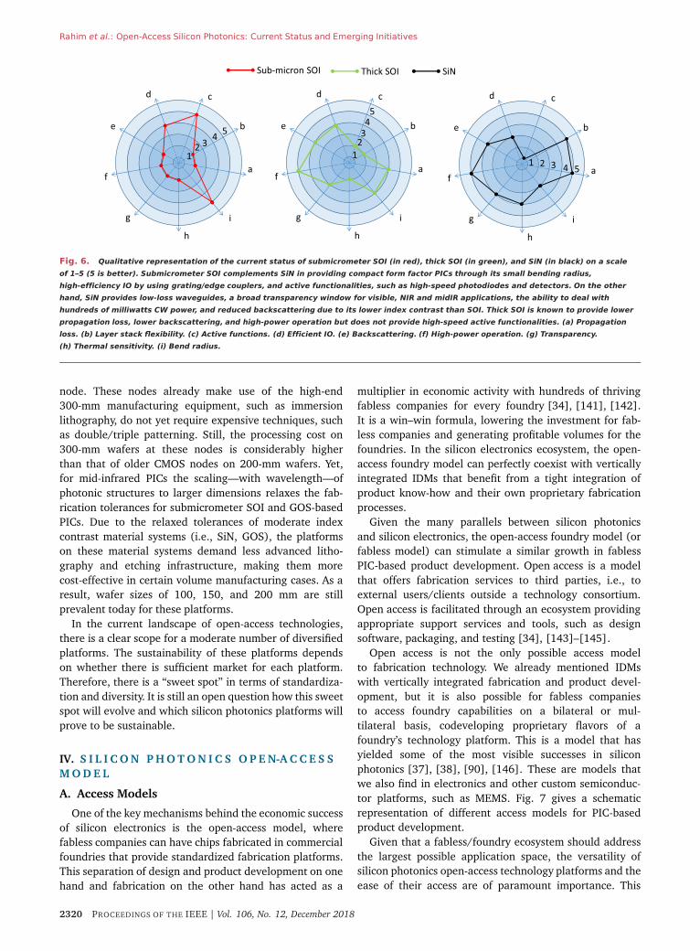
Fig. 4 gives an overview of the various single-modewaveguide cross sections possible with the different flavorsof silicon photonics platforms discussed earlier. The submi-crometer SOI and SiN platforms support fully etched stripwaveguides, deep and shallow etched rib waveguides, andslot waveguides. Specialized geometries for waveguides,such as Box-shell, are also available in the SiN-basedsilicon photonics [104]. Both submicrometer SOI and SiNmaterial systems support different types of claddings (i.e.,air and oxide). Thick SOI supports only rib waveguideswith different cladding types, whereas germanium-basedmid-infrared platforms typically support air-cladwaveguides of strip, rib, and slot types. Fig. 5 showsthe transparency range of SOI, SiN, and GOS material
2318 PROCEEDINGS OF THE IEEE | Vol. 106, No. 12, December 2018
Rahim et al.: Open-Access Silicon Photonics: Current Status and Emerging Initiatives
Fig. 4. Typical cross sections of single-mode waveguides
supported by the different variants of silicon photonics platforms.
In many cases, the air cladding is replaced by a silica cladding,
which creates a less fragile waveguide (less susceptible to dust).
systems and the corresponding applications linked tooptical transparency windows of these material systems.
E. Need for Standardization in Silicon Photonics
Each fab requires developing a standardized technologywith an established and mature process flow to providemanufacturing of silicon photonics PICs. If more fabs adoptthe same standard, fabless companies will have moresupplier options, which reduces the costs and the risks forthe silicon PIC design. However, in the current landscape ofsilicon photonics technologies, there is no single standardtechnology, rather each fab has defined its own standardtechnology. This helps them to maintain fewer processes,which results in reduced cost for a foundry.
Due to the high index contrast of the material sys-tem, dimensional control is important [31], [54], [57].For example, the process control in terms of waveguidewidth and height required for wavelength selective devicesin submicrometer SOI devices is more stringent thanfor CMOS electronics. Standardization in the processflow provides stability and repeatability in the deviceperformance for large manufacturing volumes. More-over, it helps in gauging variance in key device per-formance parameters [24], [31]. A well-understood and
Fig. 5. Different forms of silicon photonics operating from visible
to mid-IR wavelengths to provide integrated photonics solutions for
bioimaging, optical communication, and sensing.
stable device performance is crucial to develop complexphotonic integrated systems on a chip.
F. Value of Diversity in Silicon Photonics
A single standardized technology platform is notnecessarily capable of addressing the requirements forvarious applications in the very wide range of marketsectors where PIC technology can potentially bring newvalue [134]. This means that while standardization is amust for the above-mentioned technical and economicreasons, so is the diversification. This is not somethingthat is unique to silicon photonics. Again, we can drawthe comparison with electronics, where CMOS is the mostdominant technology, but which comes in a variety ofnodes with different performance and price points. On topof that, there is a diversity for targeting specialized mar-kets, such as high-power electronics, ultrahigh frequencyRF electronics, ionization radiation resistant (rad-hard)electronics, and so on.
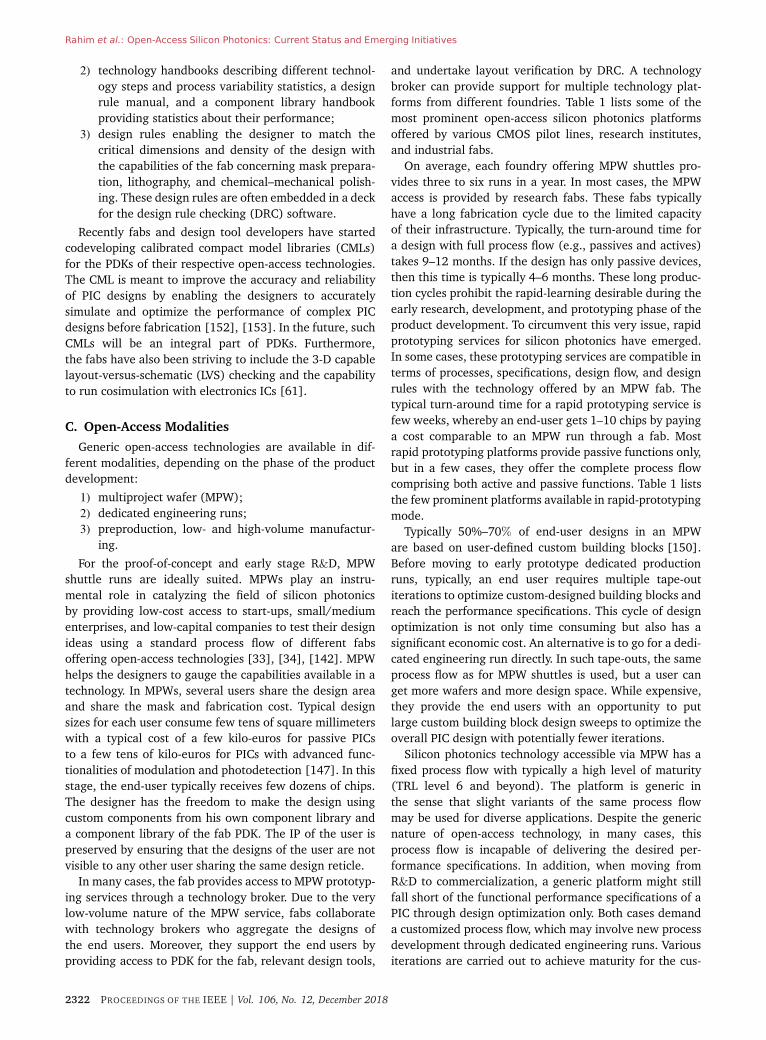
The degree of material diversity in silicon photonicsenables a situation where technology platforms comple-ment one another. Such a diversity not only preventsmonopoly of one technology platform but also developsa sense of competition between technologies and makesthem agile for evolution. As an example, Fig. 6 provides aqualitative comparison of submicrometer SOI (left), thickSOI (middle), and SiN-based (right) silicon photonics plat-forms. One can observe the complementarity of SiN (rightFig. 6) and submicrometer SOI (red lines in left Fig. 6). SOIcomplements SiN by providing compact form factor PICsthrough its small bending radius, high-efficiency fiber-chipcoupling by using grating/edge couplers, and active func-tionalities, such as high-speed photodiodes and detectors.On the other hand, SiN provides lower loss waveguides,broad transparency window for visible, NIR and mid-IRapplications, ability to deal with hundreds of milliwatts CWpower, and reduced backscattering due to its lower indexcontrast than SOI.
Table 1 lists the type of material stacks used byvarious open-access silicon photonics technologies andtheir key technical differentiators. Moreover, it is alsopossible to combine elements of different platformstogether. The manufacturing flexibility of SiN layersmakes it possible to integrate SiN layers into the SOIplatforms [108], [110], [135]–[138]. In such a platform,passive components demanding low loss and high fabrica-tion tolerance are defined on the SiN layer [139], [140].Functions, such as modulators and photodiodes, are thendefined in the Si layer.
Along with the platform diversity, there is a diversityin infrastructure needed for silicon photonics. Most of thesubmicrometer SOI platforms use 200- or 300-mm wafers.For NIR applications on submicrometer SOI, the desiredfeature sizes or CDs can be delivered by 130- or 90-nmCMOS pilot lines and foundries. However, due to the highindex contrast of submicrometer SOI, the required accu-racy corresponds more to a 40- or 65-nm CMOS technology
Vol. 106, No. 12, December 2018 | PROCEEDINGS OF THE IEEE 2319
Rahim et al.: Open-Access Silicon Photonics: Current Status and Emerging Initiatives
Fig. 6. Qualitative representation of the current status of submicrometer SOI (in red), thick SOI (in green), and SiN (in black) on a scale
of 1–5 (5 is better). Submicrometer SOI complements SiN in providing compact form factor PICs through its small bending radius,
high-efficiency IO by using grating/edge couplers, and active functionalities, such as high-speed photodiodes and detectors. On the other
hand, SiN provides low-loss waveguides, a broad transparency window for visible, NIR and midIR applications, the ability to deal with
hundreds of milliwatts CW power, and reduced backscattering due to its lower index contrast than SOI. Thick SOI is known to provide lower
propagation loss, lower backscattering, and high-power operation but does not provide high-speed active functionalities. (a) Propagation
loss. (b) Layer stack flexibility. (c) Active functions. (d) Efficient IO. (e) Backscattering. (f) High-power operation. (g) Transparency.
(h) Thermal sensitivity. (i) Bend radius.
node. These nodes already make use of the high-end300-mm manufacturing equipment, such as immersionlithography, do not yet require expensive techniques, suchas double/triple patterning. Still, the processing cost on300-mm wafers at these nodes is considerably higherthan that of older CMOS nodes on 200-mm wafers. Yet,for mid-infrared PICs the scaling—with wavelength—ofphotonic structures to larger dimensions relaxes the fab-rication tolerances for submicrometer SOI and GOS-basedPICs. Due to the relaxed tolerances of moderate indexcontrast material systems (i.e., SiN, GOS), the platformson these material systems demand less advanced litho-graphy and etching infrastructure, making them morecost-effective in certain volume manufacturing cases. As aresult, wafer sizes of 100, 150, and 200 mm are stillprevalent today for these platforms.
In the current landscape of open-access technologies,there is a clear scope for a moderate number of diversifiedplatforms. The sustainability of these platforms dependson whether there is sufficient market for each platform.Therefore, there is a “sweet spot” in terms of standardiza-tion and diversity. It is still an open question how this sweetspot will evolve and which silicon photonics platforms willprove to be sustainable.
IV. S I L I C O N P H O T O N I C S O P E N-A C C E S SM O D E L
A. Access Models
One of the key mechanisms behind the economic successof silicon electronics is the open-access model, wherefabless companies can have chips fabricated in commercialfoundries that provide standardized fabrication platforms.This separation of design and product development on onehand and fabrication on the other hand has acted as a
multiplier in economic activity with hundreds of thrivingfabless companies for every foundry [34], [141], [142].It is a win–win formula, lowering the investment for fab-less companies and generating profitable volumes for thefoundries. In the silicon electronics ecosystem, the open-access foundry model can perfectly coexist with verticallyintegrated IDMs that benefit from a tight integration ofproduct know-how and their own proprietary fabricationprocesses.
Given the many parallels between silicon photonicsand silicon electronics, the open-access foundry model (orfabless model) can stimulate a similar growth in fablessPIC-based product development. Open access is a modelthat offers fabrication services to third parties, i.e., toexternal users/clients outside a technology consortium.Open access is facilitated through an ecosystem providingappropriate support services and tools, such as designsoftware, packaging, and testing [34], [143]–[145].
Open access is not the only possible access modelto fabrication technology. We already mentioned IDMswith vertically integrated fabrication and product devel-opment, but it is also possible for fabless companiesto access foundry capabilities on a bilateral or mul-tilateral basis, codeveloping proprietary flavors of afoundry’s technology platform. This is a model that hasyielded some of the most visible successes in siliconphotonics [37], [38], [90], [146]. These are models thatwe also find in electronics and other custom semiconduc-tor platforms, such as MEMS. Fig. 7 gives a schematicrepresentation of different access models for PIC-basedproduct development.
Given that a fabless/foundry ecosystem should addressthe largest possible application space, the versatility ofsilicon photonics open-access technology platforms and theease of their access are of paramount importance. This
2320 PROCEEDINGS OF THE IEEE | Vol. 106, No. 12, December 2018

Rahim et al.: Open-Access Silicon Photonics: Current Status and Emerging Initiatives
Fig. 7. Schematic of three prominent access models for PIC
manufacturing. The first column represents vertically integrated
IDMs. They internally control the entire process from chip design to
production. Fabless companies can have joint development
programs with IDMs as represented in the second column. The third
column shows different end users submitting their PIC designs to
open-access silicon photonics pilot lines/foundries for their product
development.
allows fabless companies to develop innovative productsand evolve seamlessly from prototyping to small-volumemanufacturing and possibly all the way to high volumemanufacturing [141]. Like in electronics, this will alsorequire a certain diversity in the technology offerings,allowing product developers to pick the platform bestsuited for their application.
B. Open-Access Workflow
In an open-access model, it is important for allparties involved that fabless companies find theirway to a suitable foundry as easily and as affordablyas possible. For electronics, this was given a boostthrough the creation of the MPW service MOSISin 1981 [23], [34], [143]–[145], later mirrored byEuropractice IC in Europe [147]. For silicon photonics,ePIXfab—a joint initiative by imec (Belgium) andCommission pour l’Energie Atomique-Laboratoired’électronique des technologies de l’information(CEA-LETI) (France), operated from Ghent University(Belgium)—pioneered a similar access mechanism forsilicon photonics through MPW service since 2006.By 2011, the open-access silicon photonics technologies ofIHP and VTT Technical Research Centre of Finland werealso offered by ePIXfab.1
A similar initiative, named Optoelectronic Systems Inte-gration in Silicon (OpSIS), was launched in 2010 fromthe University of Washington and the University ofDelaware [38]. While the initiative did not sustain beyond
1Since 2015, the MPW services offered by ePIXfab have been trans-ferred to Europractice IC Service. ePIXfab has transformed itself into theEuropean Silicon Photonics Alliance, with the majority of the Europeanopen-access silicon photonics fabs as its members, and continues topromote silicon photonics science, technology, and application throughfabless models (http://epixfab.eu).
2015, it was vividly successful in providing design supportfor researchers in silicon photonics and organization ofmultiple MPW runs through fabs, such as BAE SystemsCMOS fab and the Institute of Microelectronics (IME),Singapore [37], [38]. Recently, a new initiative called theAmerican Institute for Manufacturing integrated Photonics(AIM Photonics) has emerged. It is currently engaged inestablishing an ecosystem supporting the complete siliconphotonics product development (from design to prototypeto pilot or mid-scale wafer and package manufacturing)using the 300-mm fab at The State University of New YorkPolytechnic Institute and packaging facilities in Rochester,NY, USA [148], [149].
Various other initiatives, which provide open-accesssilicon photonics technologies to end users have alsoemerged. For example, the Photonics Electronics Technol-ogy Research Association (PETRA), Japan, and the Elec-tronics & Telecommunications Research Institute (ETRI),South Korea, provide access to the end users in theserespective countries. Similarly, other countries have devel-oped open-access technologies to address the demands oflocal and/or global end users.
When an end-user wants to access PIC fabrication tech-nology, the first challenge is to determine whether thesilicon photonics technology will meet the system specifi-cation and which technology flavors from a diverse poolof foundries are most suitable. In many cases, an end-user product developer does not have the internal tech-nical know-how to make this platform selection, let alonekick-start the design of a full-custom complex PIC. As withcustom electronics, this creates a space for photonic designhouses and brokers that can support the end-user in hischoice of technology.
After the selection of technology, the open-accessprocess makes it possible to get started on a practicaldesign without the need for complex bilateral discussions.Open-access foundries provide access to process designkits (PDKs) after signing a standard design kit licenseagreement with the fab. In a case, where the PIC designis outsourced to a design house, a similar nondisclosureagreement is usually signed with the design house.
The PDK provided by the foundry is the interfacebetween the designer and the technology [150], [151].It contains sufficient technical details of the technology toenable the designer to create either full-custom layouts orcustom circuits. A PDK is typically compatible with specificdesign tools and is always foundry-specific. Unlike withelectronics, where there is some standardization of thecontent of PDKs, there is, yet, no standardized blueprintfor photonics PDKs. In its simplest form, it contains layerdescription associated with a process step and criticaldimensions that define the design rules for the processsteps. More advanced versions of PDKs also contain thefollowings:
1) component libraries with their parametric cells andtheir layouts [either actual layouts or intellectualproperty (IP)-protected black-boxes];
Vol. 106, No. 12, December 2018 | PROCEEDINGS OF THE IEEE 2321
Rahim et al.: Open-Access Silicon Photonics: Current Status and Emerging Initiatives
2) technology handbooks describing different technol-ogy steps and process variability statistics, a designrule manual, and a component library handbookproviding statistics about their performance;
3) design rules enabling the designer to match thecritical dimensions and density of the design withthe capabilities of the fab concerning mask prepara-tion, lithography, and chemical–mechanical polish-ing. These design rules are often embedded in a deckfor the design rule checking (DRC) software.
Recently fabs and design tool developers have startedcodeveloping calibrated compact model libraries (CMLs)for the PDKs of their respective open-access technologies.The CML is meant to improve the accuracy and reliabilityof PIC designs by enabling the designers to accuratelysimulate and optimize the performance of complex PICdesigns before fabrication [152], [153]. In the future, suchCMLs will be an integral part of PDKs. Furthermore,the fabs have also been striving to include the 3-D capablelayout-versus-schematic (LVS) checking and the capabilityto run cosimulation with electronics ICs [61].
C. Open-Access Modalities
Generic open-access technologies are available in dif-ferent modalities, depending on the phase of the productdevelopment:
1) multiproject wafer (MPW);2) dedicated engineering runs;3) preproduction, low- and high-volume manufactur-
ing.
For the proof-of-concept and early stage R&D, MPWshuttle runs are ideally suited. MPWs play an instru-mental role in catalyzing the field of silicon photonicsby providing low-cost access to start-ups, small/mediumenterprises, and low-capital companies to test their designideas using a standard process flow of different fabsoffering open-access technologies [33], [34], [142]. MPWhelps the designers to gauge the capabilities available in atechnology. In MPWs, several users share the design areaand share the mask and fabrication cost. Typical designsizes for each user consume few tens of square millimeterswith a typical cost of a few kilo-euros for passive PICsto a few tens of kilo-euros for PICs with advanced func-tionalities of modulation and photodetection [147]. In thisstage, the end-user typically receives few dozens of chips.The designer has the freedom to make the design usingcustom components from his own component library anda component library of the fab PDK. The IP of the user ispreserved by ensuring that the designs of the user are notvisible to any other user sharing the same design reticle.
In many cases, the fab provides access to MPW prototyp-ing services through a technology broker. Due to the verylow-volume nature of the MPW service, fabs collaboratewith technology brokers who aggregate the designs ofthe end users. Moreover, they support the end users byproviding access to PDK for the fab, relevant design tools,
and undertake layout verification by DRC. A technologybroker can provide support for multiple technology plat-forms from different foundries. Table 1 lists some of themost prominent open-access silicon photonics platformsoffered by various CMOS pilot lines, research institutes,and industrial fabs.
On average, each foundry offering MPW shuttles pro-vides three to six runs in a year. In most cases, the MPWaccess is provided by research fabs. These fabs typicallyhave a long fabrication cycle due to the limited capacityof their infrastructure. Typically, the turn-around time fora design with full process flow (e.g., passives and actives)takes 9–12 months. If the design has only passive devices,then this time is typically 4–6 months. These long produc-tion cycles prohibit the rapid-learning desirable during theearly research, development, and prototyping phase of theproduct development. To circumvent this very issue, rapidprototyping services for silicon photonics have emerged.In some cases, these prototyping services are compatible interms of processes, specifications, design flow, and designrules with the technology offered by an MPW fab. Thetypical turn-around time for a rapid prototyping service isfew weeks, whereby an end-user gets 1–10 chips by payinga cost comparable to an MPW run through a fab. Mostrapid prototyping platforms provide passive functions only,but in a few cases, they offer the complete process flowcomprising both active and passive functions. Table 1 liststhe few prominent platforms available in rapid-prototypingmode.
Typically 50%–70% of end-user designs in an MPWare based on user-defined custom building blocks [150].Before moving to early prototype dedicated productionruns, typically, an end user requires multiple tape-outiterations to optimize custom-designed building blocks andreach the performance specifications. This cycle of designoptimization is not only time consuming but also has asignificant economic cost. An alternative is to go for a dedi-cated engineering run directly. In such tape-outs, the sameprocess flow as for MPW shuttles is used, but a user canget more wafers and more design space. While expensive,they provide the end users with an opportunity to putlarge custom building block design sweeps to optimize theoverall PIC design with potentially fewer iterations.
Silicon photonics technology accessible via MPW has afixed process flow with typically a high level of maturity(TRL level 6 and beyond). The platform is generic inthe sense that slight variants of the same process flowmay be used for diverse applications. Despite the genericnature of open-access technology, in many cases, thisprocess flow is incapable of delivering the desired per-formance specifications. In addition, when moving fromR&D to commercialization, a generic platform might stillfall short of the functional performance specifications of aPIC through design optimization only. Both cases demanda customized process flow, which may involve new processdevelopment through dedicated engineering runs. Variousiterations are carried out to achieve maturity for the cus-
2322 PROCEEDINGS OF THE IEEE | Vol. 106, No. 12, December 2018

Rahim et al.: Open-Access Silicon Photonics: Current Status and Emerging Initiatives
Table 1 Prominent Open-Access Silicon Photonics Technology Platforms Offered by Various Fabs, Their Technology, and Access Mechanism
tomized processes, which makes the turn-around time ofsuch dedicated engineering runs longer than is the casewith MPW. The end users are provided with a customizedPDK with agreement on the design rules and design layersmaking these runs more flexible. Typically, a customizeddedicated engineering run costs 10× more than an MPWparticipation.
Once the PIC design has reached a certain matu-rity, the silicon photonics product development requirespreproduction engineering runs. During these runs,the process repeatability is established to ensure a pre-dictable process flow. During this phase, corner lots arerun as a critical validation step to determine the worstcase estimate of the system functional performance spec-ification. Such lots are important for defining the idealprocess conditions for low- or high-volume manufacturing.Manufacturing volumes of a few hundreds to a few thou-sands of wafers per year are considered to be low volumefor PIC manufacturing. As today most open-access tech-nologies are offered by R&D fabs, this is the only volumebracket that can be addressed, as these R&D fabs gener-ally do not have a capacity for medium- or high-volumeproduction. However, R&D fabs may have agreementswhere the end users can translate the process developed
in an R&D lab to commercial fabs providing medium- andhigh-volume manufacturing. This process transfer requiresmatched geometries (i.e., minimum feature size), a similarperformance of building blocks, including the performancevariability, matched PDK and associated device models,and migration of other parts of the supply chain (e.g.,assembly). ST Microelectronics, though an IDM, is oneof the first foundries to provide access to its technol-ogy platform for volume manufacturing through bilateralcontracts [146]. Other foundries with the capacity forhigh-volume manufacturing, such as GlobalFoundries andTowerJazz, have also announced to launch open-accesssilicon photonics platforms. Moreover, in 2017, TSMCdeveloped a through-silicon-via-enabled silicon photonicsplatform in a 300-mm foundry. This platform has demon-strated the state-of-the-art performance for various passiveand active building blocks [90].
Table 1 provides a nonexhaustive list of institutesand foundries providing (or in the process of providing)open-access silicon photonics technologies. In the earlydays, the fabs chose 220-nm SOI as the substrate for theirplatform development [24], [25], [27], [31], [41]. Morerecently, silicon photonics open-access platforms basedon 310-nm SOI [26], [40], 500-nm SOI [154], and SiN-
Vol. 106, No. 12, December 2018 | PROCEEDINGS OF THE IEEE 2323

Rahim et al.: Open-Access Silicon Photonics: Current Status and Emerging Initiatives
and germanium-based mid-infrared platforms have alsoemerged. The technology, access mechanism, and wafersize used are also listed in Table 1. Table 1 will likely evolveconsiderably in the next years.
D. Recent Open-Access Silicon PhotonicsTechnology and Ecosystem Developments
1) Process Technology: Advances in process technolo-gies for silicon photonics platforms have resulted in theirimproved performance. These improvements resulted indemonstrating passive devices with lower loss, superiorspectral accuracy, and higher reproducibility. Performanceof active devices has also benefited from the evolvedprocessing technology, whereby different types of efficientmodulators and photodetectors operating at high-speedare demonstrated [24]–[28], [31], [32], [155]–[160]. Asa result of advances in the process technology, open-accessfabs have consolidated their platforms by offering newprocess modules, such as very low-loss waveguides[155], [156], high-speed modulators [161]–[166], inte-gration of efficient electrooptic materials in a siliconphotonics process flow [173], [174], multilayer SiN onSi [108], [110], [135]–[138], and broadband fiber-chip-fiber couplers [167]–[172], [175].
Most applications of PICs require that a light sourcesupplies the chip with either a clean optical carrier (laser)or broadband light. A variety of approaches are pur-sued to bring III–V and SOI-based silicon photonicstogether [176]–[178]. Demonstrations are reported toreach the ultimate solution of a monolithically inte-grated quantum-well or quantum-dot III–V laser sourcein silicon photonics [179]–[185]. Currently, the mostmature solutions are provided by hybrid or heteroge-neously integration of quantum well or quantum dot lasersource with silicon photonics PICs [183], [186]–[188].Open-access platforms are actively engaged in develop-ing the wafer-scale integration of light-sources on sili-con PICs. Wafer-scale integration is required to preservethe cost advantage of silicon photonics. A recent demon-stration of wafer-scale heterogeneous integration oflight-sources is reported in [189]. An incumbent technol-ogy that can provide wafer-scale integrated laser sourcesis microtransfer-printing (µTP) [190]. Other open-accesstechnology consortia, such as AIM Photonics, are alsoexploring the development of integrated laser solu-tions, including quantum dot-based wafer-scale epitaxiallygrown laser sources within their silicon photonics technol-ogy platform [148], [149].
To gauge the process stability and capability of thePIC platforms offered by the open-access fabs, method-ologies and infrastructure for platform performance track-ing are developed by monitoring the key dimensionsfor each processing step [24], [191]–[193]. Furthermore,infrastructure for wafer-scale end-of-line optical, elec-trooptic, and electrical testing using automatic setups is setup to determine device performance [31], [90], [194].
2) Design Tools: Open-access technologies only makesense in combination with a design infrastructure thatenables platform users to design their own devices andstructures. We can identify two essential parts of thedesign infrastructure: design/simulation tools and PDKs.A number of design tools for PICs have emerged in the pasttwo decades [151]. At first, they supported the designer ingenerating complex layout features for photonic compo-nents, which are often much more complicated than thosefor electronics. Photonics requires curvilinear waveguidesand custom all-angle geometries, while typical electroniclayouts are based on simple rectangular features. Theresulting geometries can be simulated using electromag-netic solvers, which can be quite computationally heavy.
Today, photonic design is gradually migrating to thecircuit level [151]; instead of defining and simulatingevery individual geometry, a photonic circuit is constructedof building blocks and connected with waveguides. Eachbuilding block has an efficient compact model that is usedto calculate the response of the entire circuit. This is similarto electronic circuit design, where the compact models aredefined in SPICE or VerilogA. Photonic models can also bedefined in VerilogA [195] or in a model for a specializedphotonic circuit simulator. Such circuit-level design, whichstarts with a schematic and circuit simulation and onlythen implements the circuit as an actual layout, can scaleup to designs of much larger complexity. In addition,circuit-level design allows the user to focus on the addedvalue of his application, rather than redesigning low-levelfunctional building blocks.
Circuit design requires a library of components that canbe connected together into a circuit. For each technologyplatform, fabs supply a PDK that contains a standard com-ponent library for essential functions, such as waveguiding,splitting, crossing, modulation, detection, and fiber cou-pling. Until recently, these component libraries consistedof simple layouts that a designer could reuse at the circuitlevel, but the PDK libraries are now gradually populatedwith compact models for the building blocks, enablingdesigners to verify the circuit function in simulation.
Most photonic design tools are available as commercialsoftware. Unfortunately, at this point, there is only lim-ited interoperability between the tools of different ven-dors, even though some collaboration and standardizationactivities are emerging [196]. This also extends to theintegration of photonic design tools and electronics designautomation (EDA) tools, as we see EDA vendors graduallysupporting photonic design [197], [198].
Because high-contrast silicon photonics components areso geometry sensitive, it is important that the effectsof the fabrication process are taken into account atthe design stage. Design-for-manufacturability techniquesthat originated in electronics are now being adaptedand extended for photonics. This includes litho-friendlydesign [199], tolerant circuit design [63], use of opticalproximity corrections [200], and tiling to control patterndensities [201].
2324 PROCEEDINGS OF THE IEEE | Vol. 106, No. 12, December 2018

Rahim et al.: Open-Access Silicon Photonics: Current Status and Emerging Initiatives
To obtain a first-time-right design, an effective verifica-tion strategy is needed. This consists of two steps: DRCensures that the laid-out design can actually be fabricated,while LVS tests extract the functional circuit from a layoutand compare it to the original design intent, includingsimulation of the extracted circuit. Robust layout verifica-tion flows have also been under development to ensurethat both the mask fabrication and silicon processing willnot be affected by the inclusion of designs that are notqualified [61].
The landscape of design tools and PDKs is rapidlyevolving with new capabilities for designers being releasedevery few months. This is needed because a low-thresholddesign experience is a direct enabler to open-access tech-nology.
3) Packaging: The packaging of silicon photonics chipsis of critical importance both at the prototyping and themanufacturing level. Efforts have been made in standard-izing the packaging processes to reduce the cost of pack-aging and to improve the reliability issues associated withoptical and electrical interfaces to silicon photonics chips.Passive and automated packaging schemes are developedto cut the cost associated with photonics packaging [202].Similar to PIC layout design rules, there have been effortsto develop packaging design kits and packaging designrules for cost-effective packaging of silicon photonics chips,their thermal management, integration with electronics,and assembly of off-chip light sources. Recently, the open-access PIC Assembly and Packaging Pilot Line PixAPPhas been established in Europe to provide end users easyaccess to the packaging of PICs. Similar initiatives areemerging in other continents. For example, the open-access platform of AIM Photonics [148] and the one fromSandia National Laboratories are combined with chip scaleassembly and packaging service.
4) Emerging Silicon PIC Prototyping & Manufacturing Ini-tiatives: The success and impact ePIXfab created by pio-neering open-access silicon photonics technologies actedas a blueprint for various other players. A growing numberof initiatives, including opSIS and A*STAR IMEC, havetaken up the same model and compounded to its success,building a much broader and active community engagedin PIC-based research and development. Though OpSIShas ceased and ePIXfab handed over its brokering roleto Europractice and CMP, the ePIXfab members (IMEC,CEA-LETI, IHP, and VTT), and A*STAR IME continue toconsolidate their respective technologies by the inclusionof new process modules and enhancing their TRLs.
Recent years have seen numerous new initiatives byCMOS pilot lines and public/private research institutesto provide open-access silicon photonics technologies. Forexample, in Europe, the pilot lines PIX4Life providingPIC prototyping/manufacturing for life-science applica-tions and MIRPHAB for mid-IR applications have surfaced.A*STAR IME, which is a pioneering Asian institute provid-ing open-access silicon photonics, has started a spin-off
AMF in 2017 to provide manufacturing of silicon PICsusing the processes and technology developed by A*STARIME. In Japan, the PETRA initiative, in South Korea,the Electronics and Telecommunications Research Insti-tute, and in China, IMECAS have started providing sili-con PIC platforms to their domestic end users. In NorthAmerica, Sandia Research Laboratories and AIM Photonicshave made progress to develop and offer silicon photonicsplatforms. Anticipating a demand for high-volume PIC-manufacturing, CMOS pilot lines and research instituteshave developed routes for high-volume manufacturingthrough commercial fabs. Moreover, commercial fabs havedeveloped silicon photonics PIC platforms and startedoffering them to third-party end users.
V. C O N C L U S I O N
Open access of silicon photonics technologies, initiallyoffered by CMOS research institutes, has played an instru-mental role in making it a mainstream photonic integrationtechnology. Thanks to the continuous consolidation of thetechnology platforms offered by CMOS pilot lines andresearch institutes, low-volume manufacturing of siliconphotonics PICs is already happening. The number of fab-less companies envisaging silicon photonics products andrequiring the manufacturing of their products is rapidlyincreasing. With this clear trend in market growth andlooming demand for high-volume manufacturing by fab-less companies, pure-play foundries have started offeringopen-access silicon photonics technologies for prototypingas well as manufacturing at low- and high-volume level.
The potential penetration of silicon photonics intomarket sectors beyond optical communication furtheraugments the growth of silicon photonics. The flavor ofsilicon photonics geared toward visible wavelengths andmid-infrared wavelengths, respectively, has emerged toaddress life-science and sensing applications. There arecases where the different flavors of silicon photonics com-pete with each other, making the technology more agilefor evolution, and there are cases where these flavorscomplement each other to strengthen silicon photonicsagainst competing technologies. Since silicon photonicsis also viable at moderate volumes, many of the existingsilicon photonics flavors may grow industrially even if theytarget specialized applications.
The developments made by the open-access technologyplatforms have galvanized the silicon photonics ecosystem.A mature and complete supply chain from design to pack-aging and testing is imminent. �
A c k n o w l e d g m e n t s
The authors would like to thank Dr. T. Aalto (VTT),Prof. J. Bowers (University of California at SantaBarbara, Santa Barbara, CA, USA), Dr. C. Doerr (Aca-cia Communications, Inc.), Dr. J.-M. Fedeli (CEA-LETI,France), Dr. P. L. Guo-Qiang (Advanced Micro Foundry),Dr. A. Khanna (Elenion Technologies), Prof. T. Koch (The
Vol. 106, No. 12, December 2018 | PROCEEDINGS OF THE IEEE 2325
Rahim et al.: Open-Access Silicon Photonics: Current Status and Emerging Initiatives
University of Arizona), Prof. J. Poon (University ofToronto), Prof. H. K. Tsang (The Chinese University ofHong Kong), and Prof. L. Zimmermann (IHP) for their kind
inputs that improved the quality of this paper. R. Baetsand A. Rahim coordinate ePIXfab, the European SiliconPhotonics Alliance.
R E F E R E N C E S[1] M. Salib et al., “Silicon photonics,” Intel Technol.
J., vol. 8, no. 2, pp. 143–160, May 2004.[2] W. Bogaerts et al., “Nanophotonic waveguides in
silicon-on-insulator fabricated with CMOStechnology,” J. Lightw. Technol., vol. 23, no. 1,pp. 401–412, Jan. 2005.
[3] B. Jalali and S. Fathpour, “Silicon photonics,” J.Lightw. Technol., vol. 24, no. 12, pp. 4600–4615,Dec. 2006.
[4] A. Rickman, “The commercialization of siliconphotonics,” Nature Photon., vol. 8, pp. 579–582,Jul. 2014.
[5] A. Huang et al., “A 10 Gb/s photonic modulatorand WDM MUX/DEMUX integrated withelectronics in 0.13 µm SOI CMOS,” in IEEE Int.Solid State Circuits Conf. (ISSCC) Dig. Tech. Papers,San Francisco, CA, USA, Feb. 2006, pp. 922–929.
[6] K. Greene, “Silicon photonics comes to market,”MIT Technol. Rev., Cambridge, MA, USA, Tech.Rep. 408520, Aug. 2007. [Online]. Available:https://www.technologyreview.com/s/408520/silicon-photonics-comes-to-market/
[7] M. Paniccia, A. Liu, N. Izhaky, and A. Barkai,“Integration challenge of silicon photonics withmicroelectronics,” in Proc. 2nd IEEE Int. Conf.Group IV Photon., Antwerp, Belgium, Sep. 2005,pp. 20–22.
[8] A. Liu et al., “A high-speed silicon opticalmodulator based on a metal–oxide–semiconductorcapacitor,” Nature, vol. 427, pp. 615–618,Feb. 2004.
[9] D. Thomson et al., “Roadmap on siliconphotonics,” J. Opt., vol. 18, no. 7, p. 073003,2016.
[10] Silicon Photonics, Yole Develop., Villeurbanne,France, 2018.
[11] M. A. G. Porcel, I. Artundo, J. D. Domenech,D. Geuzebroek, R. Sunarto, and R. Hoofman,“Monolithic photonic integration for visible andshort near-infrared wavelengths: Technologiesand platforms for bio and life scienceapplications,” Adv. Opt. Technol., vol. 7, nos. 1–2,pp. 57–65, 2018.
[12] A. Jovic et al., “A MEMS actuator system for anintegrated 3-D optical coherent tomographyscanner,” J. Microelectromech. Syst., vol. 27, no. 2,pp. 259–268, Apr. 2018.
[13] Y. Li et al., “Six-beam homodyne laser Dopplervibrometry based on silicon photonicstechnology,” Opt. Express, vol. 26, no. 3,pp. 3638–3645, 2018.
[14] C. V. Poulton et al., “Coherent solid-state LIDARwith silicon photonic optical phased arrays,” Opt.Lett., vol. 42, no. 20, pp. 4091–4094, 2017.
[15] A. Martin et al., “Photonic integrated circuit basedFMCW coherent LiDAR,” J. Lightw. Technol.,vol. 36, no. 19, pp. 4640–4645, Oct. 1, 2018.
[16] A. N. Tait et al., “Neuromorphic photonicnetworks using silicon photonic weight banks,”Sci. Rep., vol. 7, Aug. 2017, Art. no. 7430.
[17] M. Lukosevicius and H. Jaeger, “Reservoircomputing approaches to recurrent neuralnetwork training,” Comput. Sci. Rev., vol. 3, no. 3,pp. 127–149, 2009.
[18] C.-S. Poon and K. Zhou, “Neuromorphic siliconneurons and large-scale neural networks:Challenges and opportunities,” Front. Neurosci.,vol. 5, p. 108, Sep. 2011.
[19] N. C. Harris et al., “Programmable Nanophotonicsfor Quantum Simulation and Machine Learning,”in Adv. Photon. (IPR, NOMA, Sensors, Netw.,SPPCom, PS), OSA Tech. Dig., 2017,Paper ITu3A.3.
[20] Y. Shen et al., “Deep learning with coherentnanophotonic circuits,” Nature Photon., vol. 11,pp. 441–446, Jul. 2017.
[21] A. Peruzz et al., “Quantum walks of correlated
photons,” Science, vol. 329, no. 5998,pp. 1500–1503, Sep. 2010.
[22] S. Paesani et al., “Experimental quantumhamiltonian learning using a silicon photonic chipand a nitrogen-vacancy electron spin in diamond,”in Proc. Conf. Lasers Electro-Opt. Eur. Eur. QuantumElectron. Conf. (CLEO/Europe-EQEC), Munich,Germany, Jun. 2017, p. 1.
[23] The MOSIS Service. Accessed: Nov. 2018. [Online].Available: https://www.mosis.com/
[24] P. Absil et al., “Reliable 50 Gb/s silicon photonicsplatform for next-generation data center opticalinterconnects,” in IEDM Tech. Dig., San Francisco,CA, USA, Dec. 2017, pp. 34.2.1–34.2.4.
[25] A. E.-J. Lim et al., “Path to silicon photonicscommercialization: 25 Gb/s platformdevelopment in a CMOS manufacturing foundryline,” in Proc. OFC, San Francisco, CA, USA, 2014,pp. 1–3.
[26] B. Szelag et al., “Multiple wavelength siliconphotonic 200 mm R+D platform for 25 Gb/s andabove applications,” Proc. SPIE, vol. 9891,p. 98911C, May 2016, doi: 10.1117/12.2228744.
[27] D. Knoll et al., “BiCMOS silicon photonicsplatform for fabrication of high-bandwidthelectronic-photonic integrated circuits,” in Proc.IEEE 16th Top. Meeting Silicon Monolithic Integr.Circuits RF Syst. (SiRF), Austin, TX, USA,Jan. 2016, pp. 46–49.
[28] E. Timurdogan et al., “AIM process design kit(AIMPDKv2.0): Silicon photonics passive andactive component libraries on a 300 mm wafer,” inOpt. Fiber Commun. Conf. OSA Tech. Dig.,Mar. 2018, pp. 1–3, Paper M3F.1.
[29] T. Aalto, M. Cherchi, M. Harjanne, F. Sun, and M.Kapulainen, “3-micron silicon photonics,” in Proc.OFC, San Francisco, CA, USA, 2018, pp. 1–3.
[30] V. Stojanovic et al., “Monolithic silicon-photonicplatforms in state-of-the-art CMOS SOIprocesses,” Opt. Express, vol. 26,pp. 13106–13121, May 2018.
[31] T. Horikawa et al., “A 300-mm silicon photonicsplatform for large-scale device integration,” IEEEJ. Sel. Topics Quantum Electron., vol. 24, no. 4,Jul./Aug. 2018, Art. no. 8200415.
[32] T.-Y. Liow et al., “Silicon modulators andgermanium photodetectors on SOI: Monolithicintegration, compatibility, and performanceoptimization,” IEEE J. Sel. Topics QuantumElectron., vol. 16, no. 1, pp. 307–315,Jan./Feb. 2010.
[33] P. Dumon, “Towards fabless silicon photonics,” inFrontiers Opt./Laser Sci. XXIV/Plasmon.Metamater./Opt. Fabr. Test., OSA Tech. Dig. (CD),2008, Paper FMG1.
[34] M. Hochberg et al., “Silicon photonics: The nextfabless semiconductor industry,” IEEE Solid StateCircuits Mag., vol. 5, no. 1, pp. 48–58, Feb. 2013.
[35] J. Pond, J. Klein, X. Wang, J. Flueckiger, and A.Liu, “A simulation tool development roadmap tosupport a scalable silicon photonics designecosystem,” in Proc. IEEE 12th Int. Conf. Group IVPhoton. (GFP), Vancouver, BC, Canada,Aug. 2015, pp. 189–190.
[36] M. Smit et al., “An introduction to InP-basedgeneric integration technology,” Semicond. Sci.Technol., vol. 29, no. 8, p. 083001, Jun. 2014.
[37] A. E.-J. Lim et al., “Path to silicon photonicscommercialization: The foundry modeldiscussion,” in Silicon Photonics III: Systems andApplications, L. Pavesi and D. J. Lockwood, Eds.Cham, Switzerland: Springer, 2016.
[38] A. E.-J. Lim et al., “Review of silicon photonicsfoundry efforts,” IEEE J. Sel. Topics QuantumElectron., vol. 20, no. 4, Jul./Aug. 2014,Art. no. 8300112.
[39] S. J. McNab, N. Moll, and Y. A. Vlasov, “Ultra-low
loss photonic integrated circuit withmembrane-type photonic crystal waveguides,”Opt. Express, vol. 11, no. 22, pp. 2927–2939,2003.
[40] F. Boeuf et al., “Silicon photonics R&D andmanufacturing on 300-mm wafer platform,” J.Lightw. Technol., vol. 34, no. 2, pp. 286–295,Jan. 15, 2016.
[41] A. H. Atabaki et al., “Integrating photonics withsilicon nanoelectronics for the next generation ofsystems on a chip,” Nature, vol. 556, pp. 349–354,Apr. 2018.
[42] T. Tsuchizawa et al., “Microphotonics devicesbased on silicon microfabrication technology,”IEEE J. Sel. Topics Quantum Electron., vol. 11,no. 1, pp. 232–240, Jan. 2005.
[43] J. S. Orcutt et al., “Open foundry platform forhigh-performance electronic-photonicintegration,” Opt. Express, vol. 20, no. 11,pp. 12222–12232, May 2012.
[44] S. Assefa et al., “A 90 nm CMOS integratedNano-Photonics technology for 25 Gbps WDMoptical communications applications,” in IEDMTech. Dig., San Francisco, CA, USA, Dec. 2012,pp. 33.8.1–33.8.3.
[45] G. Kurczveil, M. J. R. Heck, J. D. Peters, J. M.Garcia, D. Spencer, and J. E. Bowers, “Anintegrated hybrid silicon multiwavelength AWGlaser,” IEEE J. Sel. Topics Quantum Electron.,vol. 17, no. 6, pp. 1521–1527, Nov./Dec. 2011.
[46] T. Komljenovic et al., “Heterogeneous siliconphotonic integrated circuits,” J. Lightw. Technol.,vol. 34, no. 1, pp. 20–35, Jan. 1, 2016.
[47] G. Roelkens et al., “III-V/silicon photonics foron-chip and intra-chip optical interconnects,”Laser Photon. Rev., vol. 4, pp. 751–779, Nov. 2010,doi: 10.1002/lpor.200900033.
[48] B. Ben Bakir et al., “Electrically driven hybridSi/III-V Fabry–Pérot lasers based on adiabaticmode transformers,” Opt. Express, vol. 19,pp. 10317–10325, May 2011.
[49] X. Liu, R. M. Osgood, Jr., Y. A. Vlasov, and W. M. J.Green, “Mid-infrared optical parametric amplifierusing silicon nanophotonic waveguides,” NaturePhoton., vol. 4, pp. 557–560, Aug. 2010.
[50] M. M. Miloševic, P. S. Matavulj, P. Y. Yang, A.Bagolini, and G. Z. Mashanovich, “Rib waveguidesfor mid-infrared silicon photonics,” J. Opt. Soc.Amer. B, Opt. Phys., vol. 26, no. 9, pp. 1760–1766,2009.
[51] M. M. Miloševic et al., “Silicon waveguides anddevices for the mid-infrared,” Appl. Phys. Lett.,vol. 101, p. 121105, Sep. 2012.
[52] M. Muneeb et al., “Demonstration ofSilicon-on-insulator mid-infrared spectrometersoperating at 3.8 µm,” Opt. Express, vol. 21,pp. 11659–11669, May 2013.
[53] K. K. Lee, D. R. Lim, L. C. Kimerling, J. Shin, andF. Cerrina, “Fabrication of ultralow-loss Si/SiO2waveguides by roughness reduction,” Opt. Lett.,vol. 26, no. 23, pp. 1888–1890, 2001.
[54] L. Chrostowski, X. Wang, J. Flueckiger, Y. Wu, Y.Wang, and S. T. Fard, “Impact of fabricationnon-uniformity on chip-scale silicon photonicintegrated circuits,” Proc. Opt. Fiber Commun.Conf., 2014, pp. 1–3, Paper Th2A.37.
[55] F. Morichetti, A. Canciamilla, C. Ferrari, M.Torregiani, A. Melloni, and M. Martinelli,“Roughness induced backscattering in opticalsilicon waveguides,” Phys. Rev. Lett., vol. 104,p. 033902, Jan. 2010.
[56] B. Peng et al., “Distributed backscattering inproduction O-band Si nanophotonic waveguides,”Opt. Express, vol. 25, pp. 23477–23485,Sep. 2017.
[57] K. Okamoto, “Wavelength-division-multiplexingdevices in thin SOI: Advances and prospects,”
2326 PROCEEDINGS OF THE IEEE | Vol. 106, No. 12, December 2018

Rahim et al.: Open-Access Silicon Photonics: Current Status and Emerging Initiatives
IEEE J. Sel. Topics Quantum Electron., vol. 20,no. 4, Jul./Aug. 2014, Art. no. 8200410.
[58] H. Jayatilleka et al., “Wavelength tuning andstabilization of microring-based filters usingsilicon in-resonator photoconductive heaters,”Opt. Express, vol. 23, pp. 25084–25097,Sep. 2015.
[59] P. Le Maitre et al., “Impact of process variability ofactive ring resonators in a 300mm silicon photonicplatform,” in Proc. Eur. Conf. Opt. Commun.(ECOC), Valencia, Spain, Sep. 2015, pp. 1–3.
[60] M. Tran, D. Huang, T. Komljenovic, J. Peters, andA. Malik, “Ultra-low-loss silicon waveguides forheterogeneously integrated silicon/III-Vphotonics,” Appl. Sci., vol. 8, no. 7, p. 1139, 2018.
[61] F. Boeuf, J. F. Carpentier, C. Baudot, P. Le Maitre,and J.-R. Manouvrier, “Silicon photonics researchand manufacturing using a 300-mm waferplatform,” in Silicon Photonics III: Systems andApplications, L. Pavesi and D. J. Lockwood, Eds.Cham, Switzerland: Springer, 2016.
[62] Z. Lu et al., “Performance prediction for siliconphotonics integrated circuits withlayout-dependent correlated manufacturingvariability,” Opt. Express, vol. 25, pp. 9712–9733,May 2017.
[63] S. Dwivedi, H. D’heer, and W. Bogaerts,“Maximizing fabrication and thermal tolerances ofall-silicon FIR wavelength filters,” IEEE Photon.Technol. Lett., vol. 27, no. 8, pp. 871–874,Apr. 15, 2015.
[64] Q. Lin, O. J. Painter, and G. P. Agrawal, “Nonlinearoptical phenomena in silicon waveguides:Modeling and applications,” Opt. Express, vol. 15,no. 25, pp. 16604–16644, Dec. 2007.
[65] B. Kuyken et al., “Frequency conversion ofmid-infrared optical signals into the telecom bandusing nonlinear silicon nanophotonic wires,” inProc. Opt. Fiber Commun. Conf./Nat. Fiber Opt.Eng. Conf., 2011, pp. 1–3, Paper OThU4.
[66] B. Jalali, “Silicon photonics: Nonlinear optics inthe mid-infrared,” Nature Photon., vol. 4, no. 8,pp. 506–508, 2010.
[67] R. A. Soref, J. Schmidtchen, and K. Petermann,“Large single-mode rib waveguides in GeSi-Si andSi-on-SiO2,” IEEE J. Quantum Electron., vol. 27,no. 8, pp. 1971–1974, Aug. 1991.
[68] A. G. Rickman, G. T. Reed, and F. Namavar,“Silicon-on-insulator optical rib waveguide lossand mode characteristics,” J. Lightw. Technol.,vol. 12, no. 10, pp. 1771–1776, Oct. 1994.
[69] U. Fischer, T. Zinke, J. R. Kropp, F. Arndt, andK. Petermann, “0.1 dB/cm waveguide losses insingle-mode SOI rib waveguides,” IEEE Photon.Technol. Lett., vol. 8, no. 5, pp. 647–648,May 1996.
[70] T. Aalto, K. Solehmainen, M. Harjanne, M.Kapulainen, and P. Heimala, “Low-loss convertersbetween optical silicon waveguides of differentsizes and types,” IEEE Photon. Technol. Lett.,vol. 18, no. 5, pp. 709–711, Mar. 2006.
[71] S. Nakamura, S. Takahashi, M. Sakauchi, T. Hino,M. Yu, and G. Lo, “Wavelength selective switchingwith one-chip silicon photonic circuit including8×8 matrix switch,” in Proc. Opt. Fiber Commun.Conf. Expo. Nat. Fiber Opt. Eng. Conf., Los Angeles,CA, USA, 2011, pp. 1–3.
[72] B. Schueppert et al., “Integrated optics in siliconand SiGe-heterostructures,” J. Lightw. Technol.,vol. 14, no. 10, pp. 2311–2323, Oct. 1996.
[73] T. Aalto, M. Cherchi, M. Harjanne, S. Ylinen, M.Kapulainen, and T. Vehmas, “Launching ofmulti-project wafer runs in ePIXfab withmicron-scale silicon rib waveguide technology,”Proc. SPIE, vol. 8990, p. 899003, Mar. 2014.
[74] L. Zimmermann, K. Voigt, G. Winzer,K. Petermann, and C. M. Weinert, “C-band optical90-hybrids based on silicon-on-insulator 4×4waveguide couplers,” IEEE Photon. Tech. Lett.,vol. 21, no. 3, pp. 143–145, Feb. 1, 2009.
[75] S. A. Miller et al., “Low-loss silicon platform forbroadband mid-infrared photonics,” Optica, vol. 4,no. 7, pp. 707–712, Jul. 2017.
[76] Y. Z. Tang, W. H. Wang, T. Li, and Y. L. Wang,“Integrated waveguide turning mirror in
silicon-on-insulator,” IEEE Photon. Technol. Lett.,vol. 14, no. 1, pp. 68–70, Jan. 2002.
[77] M. Cherchi, S. Ylinen, M. Harjanne,M. Kapulainen, and T. Aalto, “Dramatic sizereduction of waveguide bends on a micron-scalesilicon photonic platform,” Opt. Express, vol. 21,pp. 17814–17823, Jul. 2013.
[78] K. Vyrsokinos et al., “DPSK-Demodulation basedon Ultra-Compact micron-scale SOI platform,” inProc. Opt. Fiber Commun. Conf., 2015, pp. 1–3,Paper W2A.14.
[79] M. Pagani et al., “Low-error and broadbandmicrowave frequency measurement in a siliconchip,” Optica, vol. 2, no. 8, pp. 751–756,Aug. 2015.
[80] M. Moralis-Pegios et al., “Multicast-enablingoptical switch design employing Si buffering androuting elements,” IEEE Photon. Technol. Lett.,vol. 30, no. 8, pp. 712–715, Apr. 15, 2018.
[81] M. Harjanne, M. Kapulainen, T. Aalto, and P.Heimala, “Sub-µs switching time insilicon-on-insulator Mach-Zehnder thermo-opticswitch,” IEEE Photon. Technol. Lett., vol. 16, no. 9,pp. 2039–2041, Sep. 2004.
[82] D. Feng et al., “High-speed GeSi electroabsorptionmodulator on the SOI waveguide platform,” IEEEJ. Sel. Topics Quantum Electron., vol. 19, no. 6,Nov./Dec. 2013, Art. no. 3401710.
[83] D. Feng et al., “High-speed receiver technology onthe SOI platform,” IEEE J. Sel. Topics QuantumElectron., vol. 19, no. 2, Mar./Apr. 2013,Art. no. 3800108.
[84] C. Minkenberg et al., “Reimagining datacentertopologies with integrated silicon photonics,”IEEE/OSA J. Opt. Commun. Netw., vol. 10, no. 7,pp. 126–139, Jul. 2018.
[85] C. Gunn, “CMOS photonics for high-speedinterconnects,” IEEE Micro, vol. 26, no. 2,pp. 58–66, Mar. 2006.
[86] G. Denoyer et al., “Hybrid silicon photonic circuitsand transceiver for 50 Gb/s NRZ transmissionover single-mode fiber,” J. Lightw. Technol.,vol. 33, no. 6, pp. 1247–1254, Mar. 15, 2015.
[87] X. R. Zhang, W. H. Zhu, B. P. Liew, M. Gaurav,A. Yeo, and K. C. Chan, “Copper pillar bumpstructure optimization for flip chip packaging withCu/Low-K stack,” in Proc. 11th Int. Therm., Mech.Multi-Phys. Simulation, Exp. Microelectron.Microsyst. (EuroSimE), Bordeaux, France,Apr. 2010, pp. 1–7.
[88] J. M. Fedeli et al., “Photonic–electronic integrationwith bonding,” IEEE J. Sel. Topics QuantumElectron., vol. 20, no. 4, pp. 350–358,Jul./Aug. 2014.
[89] Y. Chen et al., “A 25 Gb/s hybrid integrated siliconphotonic transceiver in 28 nm CMOS and SOI,” inIEEE Int. Solid-State Circuits Conf. (ISSCC) Dig.Tech. Papers, San Francisco, CA, USA, Feb. 2015,pp. 1–3.
[90] P. A. De Dobbelaere, “Advanced silicon photonicstechnology platform leveraging a semiconductorsupply chain,” in IEDM Tech. Dig., San Francisco,CA, USA, Dec. 2017, pp. 34.1.1–34.1.4.
[91] C. Batten et al., “Building many-coreprocessor-to-DRAM networks with monolithicCMOS silicon photonics,” IEEE Micro, vol. 29,no. 4, pp. 8–21, Jul. 2009.
[92] D. J. Shin et al., “Integration of Si photonics intoDRAM process,” in Proc. Opt. Fiber Commun. Conf.Expo. Nat. Fiber Optic Eng. Conf. (OFC/NFOEC),Anaheim, CA, USA, Mar. 2013, pp. 1–3.
[93] M. Georgas et al., “A monolithically-integratedoptical transmitter and receiver in a zero-change45 nm SOI process,” in Proc. Symp. VLSI CircuitsDig. Tech. Papers, Honolulu, HI, USA, Jun. 2014,pp. 1–2.
[94] S. Assefa et al., “A 90 nm CMOS integratednano-photonics technology for 25 Gbps WDMoptical communications applications,” in IEDMTech. Dig., 2012, pp. 33.8.1–33.8.3.
[95] H. Abediasl and H. Hashemi, “Monolithic opticalphased-array transceiver in a standard SOI CMOSprocess,” Opt. Express, vol. 23, no. 5,pp. 6509–6519, 2015.
[96] L. Zimmermann et al., “Monolithically integrated
10 Gbit/sec Silicon modulator with driver in 0.25µm SiGe:C BiCMOS,” Proc. 39th Eur. Conf. Exhib.Opt. Commun. (ECOC), London, U.K., 2013,pp. 1–3.
[97] J. S. Orcutt et al., “Nanophotonic integration instate-of-the-art CMOS foundries,” Opt. Express,vol. 19, no. 3, pp. 2335–2346, Jan. 2011.
[98] D. Knoll et al., “Monolithically integrated 25Gbit/sec receiver for 1.55 µm in photonicBiCMOS technology,” in Proc. Opt. Fiber Commun.(OFC) Conf., 2014, pp. 1–2, Paper Th4C.4.
[99] C. H. Henry, R. F. Kazarinov, H. J. Lee,K. J. Orlowsky, and L. E. Katz, “Low lossSi3N4–SiO2 optical waveguides on Si,” Appl.Opt., vol. 26, no. 13, pp. 2621–2624, 1987.
[100] J. F. Bauters et al., “Ultra-low-loss single-modeSi3N4 waveguides with 0.7 dB/m propagationloss,” in Proc. 37th Eur. Conf. Expo. Opt. Commun.,Sep. 2011, pp. 1–3, Paper Th.12.LeSaleve.3.
[101] A. Rahim et al., “Expanding the silicon photonicsportfolio with silicon nitride photonic integratedcircuits,” J. Lightw. Technol., vol. 35, no. 4,pp. 639–649, Feb. 15, 2017.
[102] M. J. R. Heck, J. F. Bauters, M. L. Davenport,D. T. Spencer, and J. E. Bowers, “Ultra-low losswaveguide platform and its integration withsilicon photonics,” Laser Photon. Rev., vol. 8, no. 5,Sep. 2014, pp. 667–686.
[103] C. G. H. Roeloffzen et al., “Low-loss Si3N4 TriPleXoptical waveguides: Technology and applicationsoverview,” IEEE J. Sel. Topics Quantum Electron.,vol. 24, no. 4, Jul./Aug. 2018, Art. no. 4400321.
[104] A. Leinse et al., “TriPleX: The versatile siliconnitride waveguide platform,” in Proc. Prog.Electromagn. Res. Symp. (PIERS), Shanghai, China,2016, p. 67.
[105] L. Hoffman et al., “Low loss CMOS-compatiblePECVD silicon nitride waveguides and gratingcouplers for blue light optogenetic applications,”IEEE Photon. J., vol. 8, no. 5, Oct. 2016,Art. no. 2701211.
[106] Z. Zhang, M. Yako, K. Ju, N. Kawai, and K. Wada,“A silicon nitride platform by physical vapordeposition for dense wavelength divisionmultiplexing on chip,” in Proc. 11th Int. Conf.Group IV Photon. (GFP), Paris, France, Aug. 2014,pp. 193–194.
[107] C. Baudot et al., “Advanced solutions in siliconphotonics using traditional fabrication methodsand materials of CMOS technologies,” Proc. SPIE,vol. 10537, p. 105370G, Apr. 2018.
[108] S. Guerber et al., “Integrated SiN on SOI dualphotonic devices for advanced datacomsolutions,” Proc. SPIE, vol. 10686, p. 106860W,Aug. 2018, doi: 10.1117/12.2306160.
[109] J. F. Song, Q. Fang, S. H. Tao, M. B. Yu, G. Q. Lo,and D. L. Kwong, “Silicon nitride-based compactdouble-ring resonator comb filter with flat-topresponse,” IEEE Photon. Technol. Lett., vol. 20,no. 24, pp. 2156–2158, Dec. 15, 2008.
[110] Y. Huang et al., “CMOS compatible monolithicmulti-layer Si3N4-on-SOI platform for low-losshigh performance silicon photonics denseintegration,” Opt. Express, vol. 22, no. 18,pp. 21859–21865, 2014.
[111] D. J. Moss, R. Morandotti, A. L. Gaeta, and M.Lipson, “New CMOS-compatible platforms basedon silicon nitride and Hydex for nonlinear optics,”Nature Photon., vol. 7, pp. 597–607, Aug. 2013,doi: 10.1038/nphoton.2013.183.
[112] J. F. Bauters et al., “Ultra-low-losshigh-aspect-ratio Si3N4 waveguides,” Opt.Express, vol. 19, pp. 3163–3174, Feb. 2011.
[113] D. Melati, A. Melloni, and F. Morichetti, “Realphotonic waveguides: guiding light throughimperfections,” Adv. Opt. Photon., vol. 6,pp. 156–224, Jun. 2014.
[114] M. H. P. Pfeiffer et al., “Photonic damasceneprocess for integrated high-Q microresonatorbased nonlinear photonics,” Optica, vol. 3, no. 1,pp. 20–25, 2016.
[115] B. Kuyken, “Four-wave-mixing indispersion-engineered silicon nanophotoniccircuits for telecommunication and sensingapplications,” M.S. thesis, Dept. Inf. Technol.,
Vol. 106, No. 12, December 2018 | PROCEEDINGS OF THE IEEE 2327

Rahim et al.: Open-Access Silicon Photonics: Current Status and Emerging Initiatives
Ghent Univ., Ghent, Belgium, 2013,pp. 2012–2013.
[116] J. S. Penades, A. Z. Khokhar, M. Nedeljkovic, andG. Z. Mashanovich, “Low-loss mid-infrared SOIslot waveguides,” IEEE Photon. Technol. Lett.,vol. 27, no. 11, pp. 1197–1199, Jun. 1, 2015.
[117] T. Hu et al., “Silicon photonic platforms formid-infrared applications,” Photon. Res., vol. 5,no. 5, pp. 417–430, 2017.
[118] J. S. Penades et al., “Suspended siliconmid-infrared waveguide devices withsubwavelength grating metamaterial cladding,”Opt. Express, vol. 24, no. 20, pp. 22908–22916,2016.
[119] J. S. Penadés et al., “Suspended siliconwaveguides for long-wave infrared wavelengths,”Opt. Lett., vol. 43, no. 4, pp. 795–798, 2018.
[120] W. Zhou, Z. Cheng, X. Wu, B. Zhu, X. Sun, and H.K. Tsang, “Fully suspended slot waveguides forhigh refractive index sensitivity,” Opt. Lett.,vol. 42, no. 7, pp. 1245–1248, 2017.
[121] W. Zhou, Z. Cheng, X. Wu, X. Sun, and H. K.Tsang, “Fully suspended slot waveguide platform,”J. Appl. Phys., vol. 123, no. 6, p. 063103, 2018.
[122] R. Soref, “Mid-infrared photonics in silicon andgermanium,” Nature Photon., vol. 4, pp. 495–497,Aug. 2010.
[123] A. Malik, M. Muneeb, Y. Shimura, J. vanCampenhout, R. Loo, and G. Roelkens,“Germanium-on-silicon mid-infrared waveguidesand Mach-Zehnder interferometers,” in Proc. IEEEPhoton. Conf., Nov. 2013, pp. 103–104.
[124] A. Malik et al., “Ge-on-Si wavelength divisionmultiplexing components near 4.7 µm,” in Proc.Conf. Lasers Electro-Opt., 2018, pp. 1–3, PaperJW2A.39.
[125] J. Fedeli and S. Nicoletti, “Mid-infrared (Mid-IR)silicon-based photonics,” Proc. IEEE, to bepublished, doi: 10.1109/JPROC.2018.2844565.
[126] V. M. Lavchiev and B. Jakoby, “Photonics in themid-infrared: Challenges in single-chip integrationand absorption sensing,” IEEE J. Sel. TopicsQuantum Electron., vol. 23, no. 2, pp. 452–463,Mar./Apr. 2017.
[127] U. Younis et al., “Germanium-on-SOI waveguidesfor mid-infrared wavelengths,” Opt. Express,vol. 24, no. 11, pp. 11987–11993, 2016.
[128] U. Younis et al., “Towards low-loss waveguides inSOI and Ge-on-SOI for mid-IR sensing,” J. Phys.Commun., vol. 2, no. 4, p. 045029, 2018.
[129] J. Kang, M. Takenaka, and S. Takagi, “Novel Gewaveguide platform on Ge-on-insulator wafer formid-infrared photonic integrated circuits,” Opt.Express, vol. 24, no. 11, pp. 11855–11864, 2016.
[130] W. Li et al., “Germanium-on-silicon nitridewaveguides for mid-infrared integratedphotonics,” Appl. Phys. Lett., vol. 109, no. 24,p. 241101, 2016.
[131] P. Barritault et al., “Design, fabrication andcharacterization of an AWG at 4.5 µm,” Opt.Express, vol. 23, no. 20, pp. 26168–26181, 2015.
[132] J. Kang et al., “Focusing subwavelength gratingcoupler for mid-infrared suspended membranegermanium waveguides,” Opt. Lett., vol. 42,pp. 2094–2097, Jun. 2017.
[133] T.-H. Xiao et al., “Mid-infrared high-Q germaniumnanocavity,” Photon. Res., vol. 6, pp. 925–928,Sep. 2018.
[134] D. X. Xu et al., “Silicon photonic integrationplatform—Have we found the sweet spot?” IEEE J.Sel. Topics Quantum Electron., vol. 20, no. 4,pp. 189–205, Jul./Aug. 2014.
[135] J. K. S. Poon et al., “Integrated photonic devicesand circuits in multilayer silicon nitride-on-siliconplatforms,” in Proc. Opt. Fiber Commun. Conf.Exhib., Los Angeles, CA, USA, 2015, pp. 1–3,doi: 10.1364/OFC.2015.Th3F.1.
[136] J. F. Bauters, W. D. Sacher, Y. Huang, and G.-Q. Lo,“Silicon on ultra-low-loss waveguide photonicintegration platform,” Opt. Express, vol. 21, no. 1,pp. 544–555, 2013.
[137] W. D. Sacher et al., “Tri-layer siliconnitride-on-silicon photonic platform forultra-low-loss crossings and interlayertransitions,” Opt. Express, vol. 25,
pp. 30862–30875, Dec. 2017.[138] W. D. Sacher et al., “Monolithically integrated
multilayer silicon nitride-on-silicon waveguideplatforms for 3-d photonic circuits and devices,”Proc. IEEE, to be published, doi:10.1109/JPROC.2018.2860994.
[139] C. Doerr et al., “Single-chip silicon photonics100-Gb/s coherent transceiver,” Proc. Opt. FiberCommun. Conf. Exhib., San Francisco, CA, USA,2014, pp. 1–3.
[140] L. Chen, C. R. Doerr, P. Dong, and Y.-K. Chen,“Monolithic silicon chip with 10 modulatorchannels at 25 Gbps and 100-GHz spacing,” Opt.Express, vol. 19, no. 26, pp. B946–B951, 2011.
[141] R. Baets, “Building a sustainable future for siliconphotonics,” in Proc. 8th Int. Conf. Group IVPhoton., London, U.K., 2011, pp. 3–4.
[142] A. Novack et al., “Progress in silicon platforms forintegrated optics,” Nanophotonics, vol. 3, nos. 4–5,pp. 205–214, 2018,doi: 10.1515/nanoph-2013-0034.
[143] L. Conway, “Impact of the Mead-Conwayinnovations in VLSI chip design andimplementation methodology,” Univ. Michigan,Ann Arbor, MI, USA, White Paper.
[144] M. Hochberg and T. Baehr-Jones, “Towards fablesssilicon photonics,” Nature Photon., vol. 4, no. 8,p. 492, 2010, doi: 10.1038/nphoton.2010.172.
[145] R. Baets et al., “Silicon photonics,” in Proc. Int.Symp. VLSI Technol., Syst. Appl. (VLSI-TSA),Hsinchu, Taiwan, 2007, pp. 1–3.
[146] F. Boeuf et al., “Recent progress in siliconphotonics R&D and manufacturing on 300 mmwafer platform,” in Proc. Opt. Fiber Commun. Conf.Exhib. (OFC), Los Angeles, CA, USA, 2015,pp. 1–3.
[147] The Europractice IC Service. Accessed: Nov. 2018.[Online]. Available:http://www.europractice-ic.com
[148] M. Liehr et al., “AIM photonics—What mergingphotonics with nano-electronics will do,” in Proc.IEEE Opt. Interconnects Conf. (OI),San Diego, CA, USA, May 2016, pp. 22–23.
[149] T. L. Koch et al., “The american institute formanufacturing integrated photonics: Advancingthe ecosystem,” Proc. SPIE, vol. 9772, p. 977202,Feb. 2016.
[150] M. Heins et al., “Design flow automation forsilicon photonics: Challenges, collaboration, andstandardization,” in Silicon Photonics III: Systemsand Applications, L. Pavesi and D. J. Lockwood,Eds. Cham, Switzerland: Springer, 2016.
[151] W. Bogaerts and L. Chrostowski, “Siliconphotonics circuit design: Methods, tools andchallenges,” Laser Photon. Rev., vol. 12, no. 4,p. 1700237, Mar. 2018.
[152] Z. Zhang et al., “Compact modeling for siliconphotonic heterogeneously integrated circuits,” J.Lightw. Technol., vol. 35, no. 14, pp. 2973–2980,Jul. 15, 2017.
[153] L. Chrostowski and M. Hochberg, Silicon PhotonicsDesign: From Devices to Systems. Cambridge, U.K.:Cambridge Univ. Press, 2015.
[154] X. Chen et al., “The emergence of siliconphotonics as a flexible technology platform,” Proc.IEEE, doi: 10.1109/JPROC.2018.2854372.
[155] T. Mogami et al., “High-performance siliconphotonics process platform for low-powerphotonic integrated circuits,” in Proc. IEEE SiliconNanoelectron. Workshop (SNW), Honolulu, HI,USA, Jun. 2016, pp. 216–217.
[156] S. K. Selvaraja et al., “Highly uniform and low-losspassive silicon photonics devices using a 300 mmCMOS platform,” in Proc. Opt. Fiber Commun.Conf. Exhib., San Francisco, CA, USA, 2014,pp. 1–3, doi: 10.1364/OFC.2014.Th2A.33.
[157] J. Park, G. Kim, H. Park, J. Joo, S. Kim, and M.-J.Kwack, “Performance improvement in siliconarrayed waveguide grating by suppression ofscattering near the boundary of a star coupler,”Appl. Opt., vol. 54, no. 17, pp. 5597–5602,Jun. 2015.
[158] T. Horikawa, D. Shimura, S.-H. Jeong, M.Tokushima, K. Kinoshita, and T. Mogami, “Theimpacts of fabrication error in Si wire-waveguides
on spectral variation of coupled resonator opticalwaveguides,” Microelectron. Eng., vol. 156,pp. 46–49, Apr. 2016.
[159] T. Horikawa et al., “Resonant wavelengthvariation modelling for microring resonatorsbased on fabrication deviation analysis,” in Proc.43rd Eur. Conf. Opt. Commun., Gothenburg,Sweden, Sep. 2017, pp. 1–3.
[160] H. Okayama, Y. Onawa, D. Shimura, H. Takahashi,H. Yaegashi, and H. Sasaki, “Low loss 100 GHzspacing Si arrayed-waveguide grating usingminimal terrace at slab–array interface,” Electron.Lett., vol. 52, no. 18, pp. 1545–1546, Sep. 2016.
[161] M. Li, L. Wang, X. Li, X. Xiao, and S. Yu, “Siliconintensity Mach–Zehnder modulator for single lane100 Gb/s applications,” Photon. Res., vol. 6, no. 2,pp. 109–116, 2018.
[162] X. Xiao, M. Li, L. Wang, D. Chen, Q. Yang, and S.Yu, “High speed silicon photonic modulators,” inProc. Opt. Fiber Commun. Conf., Mar. 2017,pp. 1–3, Paper Tu2H.1.
[163] E. Timurdogan et al., “An ultralow power athermalsilicon modulator,” Nature Commun. vol. 5,Jun. 2014, Art. no. 4008.
[164] K. Goi et al., “DQPSK/QPSK modulation at 40–60Gb/s using low-loss nested silicon Mach-Zehndermodulator,” in Proc. Opt. Fiber Commun.Conf./Nat. Fiber Opt. Eng. Conf., 2013, pp. 1–3,Paper OW4J.4.
[165] B. Milivojevic et al., “Demonstration of opticaltransmission at bit rates of up to 321.4 Gb/s usingcompact silicon based modulator and linearBiCMOS MZM driver,” in Proc. Opt. FiberCommun. Conf., 2016, pp. 1–3, Paper Th1F.2.
[166] A. Samani et al., “A low-voltage 35-GHz siliconphotonic modulator-enabled 112-Gb/stransmission system,” IEEE Photon. J., vol. 7,no. 3, Jun. 2015, Art. no. 7901413.
[167] W. D. Sacher et al., “Wide bandwidth and highcoupling efficiency Si3N4-on-SOI dual-levelgrating coupler,” Opt. Express, vol. 22,pp. 10938–10947, May 2014.
[168] J. Notaros et al., “Ultra-efficient CMOSfiber-to-chip grating couplers,” in Proc. Opt. FiberCommun. Conf. Exhib. (OFC), Anaheim, CA, USA,2016, pp. 1–3.
[169] W. Zhou, Z. Cheng, X. Sun, and H. K. Tsang,“Tailorable dual-wavelength-band coupling in atransverse-electric-mode focusing subwavelengthgrating coupler,” Opt. Lett., vol. 43, no. 12,pp. 2985–2988, 2018.
[170] T. Barwicz and Y. Taira, “Low-cost interfacing offibers to nanophotonic waveguides: Design forfabrication and assembly tolerances,” IEEE Photon.J., vol. 6, no. 4, Aug. 2014, Art. no. 6600818.
[171] C. E. Png et al., “Optimized optical devices foredge-coupling-enabled silicon photonicsplatform,” Proc. SPIE, vol. 10537, p. 105371L,Feb. 2018.
[172] R. Marchetti et al., “High-efficiencygrating-couplers: Demonstration of a new designstrategy,” Sci. Rep., vol. 7, no. 1, 2017,Art. no. 16670.
[173] F. Eltes et al., “A novel 25 Gbps electro-opticPockels modulator integrated on an advanced Siphotonic platform,” in IEDM Tech. Dig., Dec. 2017,pp. 27-5.1–27-5.4.
[174] K. Alexander, J. P. George, B. Kuyken, J.Beeckman, and D. van Thourhout, “Broadbandelectro-optic modulation using low-lossPZT-on-silicon nitride integrated waveguides,” inProc. Conf. Lasers Electro-Opt., 2017, pp. 1–3,Paper JTh5C.7.
[175] B. Ben Bakir et al., “Low-Loss (< 1 dB) andpolarization-insensitive edge fiber couplersfabricated on 200-mm silicon-on-insulatorwafers,” IEEE Photon. Technol. Lett., vol. 22,no. 11, pp. 739–741, Jun. 1, 2010.
[176] G. H. Duan et al., “Hybrid III–V on silicon lasersfor photonic integrated circuits on silicon,” IEEE J.Sel. Topics Quantum Electron., vol. 20, no. 4,pp. 158–170, Jul./Aug. 2014.
[177] L. Diang and J. E. Bowers, “Recent progress inlasers on silicon,” Nature Photon., vol. 4, no. 8,pp. 511–517, 2010.
2328 PROCEEDINGS OF THE IEEE | Vol. 106, No. 12, December 2018

Rahim et al.: Open-Access Silicon Photonics: Current Status and Emerging Initiatives
[178] T. Shimizu et al., “High density hybrid integratedlight source with a laser diode array on a siliconoptical waveguide platform for inter-chip opticalinterconnection,” Proc. 8th IEEE Int. Conf. GroupIV Photon., London, U.K., Sep. 2011,pp. 181–183.
[179] J. B. Rodriguez, L. Cerutti, P. Grech, andE. Tournié, “Room-temperature operation of a2.25 µm electrically pumped laser fabricated on asilicon substrate,” Appl. Phys. Lett., vol. 94, no. 6,p. 061124, 2009.
[180] Z. Whang et al., “Room-temperature InPdistributed feedback laser array directly grown onsilicon,” Nature Photon., vol. 9, pp. 837–842,Dec. 2015.
[181] S. Chen et al., “Electrically pumpedcontinuous-wave III–V quantum dot lasers onsilicon,” Nature Photon., vol. 10, no. 5,pp. 307–311, 2016.
[182] S. Wirths et al., “Lasing in direct-bandgap GeSnalloy grown on Si,” Nature Photon., vol. 9, no. 2,pp. 88–92, 2015.
[183] Y. Urino et al., “First demonstration of athermalsilicon optical interposers with quantum dot lasersoperating up to 125 ◦C,” J. Lightw. Technol.,vol. 33, no. 6, pp. 1223–1229, Mar. 15, 2015.
[184] T. Wang, H. Liu, A. Lee, F. Pozzi, and A. Seeds,“1.3-µm InAs/GaAs quantum-dot lasersmonolithically grown on Si substrates,” Opt.Express, vol. 19, no. 12, pp. 11381–11386, 2011.
[185] S. Chen et al., “1.3-µm InAs/GaAs quantum-dotlaser monolithically grown on Si substratesoperating over 100 ◦C,” Electron. Lett., vol. 50,no. 20, pp. 1467–1468, 2014.
[186] G. Roelkens et al., “III-V-on-silicon photonicdevices for optical communication and sensing,”Photonics, vol. 2, no. 3, pp. 969–1004, 2015.
[187] A. Y. Liu et al., “Quantum dot lasers for siliconphotonics,” Photon. Res., vol. 3, no. 5, pp. B1–B9,2015.
[188] K. Tanabe and Y. Arakawa, “1.3 µm InAs/GaAsquantum dot lasers on SOI waveguide structures,”in Proc. CLEO, Sci. Innov., 2014, pp. 1–3, PaperSTh1G.6.
[189] B. Szelag et al., “Hybrid III-V/Si DFB laserintegration on a 220 mm fully CMOS-compatiblesilionn photonlcsplotform,” IEDM Tech. Dig., SanFrancisco, CA, USA, Dec. 2017, pp. 24.1.1–24.1.4.
[190] J. Zhang et al., “Transfer-printing-basedintegration of a III-V-on-silicon distributedfeedback laser,” Opt. Express, vol. 26, no. 7,pp. 8821–8830, 2018.
[191] T. Horikawa et al., “Process control andmonitoring in device fabrication for opticalinterconnection using silicon photonicstechnology,” in Proc. IEEE Int. Interconnect Technol.Conf. IEEE Mater. Adv. Metallization Conf.(IITC/MAM), Grenoble, France, May 2015,pp. 277–280.
[192] F. Boeuf et al., “Silicon photonics R&D andmanufacturing on 300-mm wafer platform,”J. Lightw. Technol., vol. 34, no. 2, pp. 286–295,Jan. 15, 2016.
[193] W. A. Zortman, D. C. Trotter, and M. R. Watts,“Silicon photonics manufacturing,” Opt. Express,vol. 18, pp. 23598–23607, Oct. 2010.
[194] J. De Coster et al., “Test-station for flexiblesemi-automatic wafer-level silicon photonics
testing,” in Proc. IEEE Eur. Test Symp., Amsterdam,The Netherlands, May 2016, pp. 1–6.
[195] C. Sorace-Agaskar, J. Leu, M. R. Watts, and V.Stojanovic, “Electro-optical co-simulation forintegrated CMOS photonic circuits with VerilogA,”Opt. Express, vol. 23, no. 21, pp. 27180–27203,2015.
[196] The PDAFlow Foundation. Accessed: Nov. 2018.[Online]. Available: http://www.pdaflow.org
[197] A. Farsaei et al., “A novel and scalable designmethodology for the simulation of photonicintegrated circuits,” in Adv. Photon. OSA Tech.Dig., 2016, pp. 1–3, Paper JTu4A.2.
[198] W. Bogaerts, M. Fiers, M. Sivilotti, and P. Dumon,“The IPKISS photonic design framework,” in Proc.Opt. Fiber Commun. Conf., 2016, pp. 1–3, PaperW1E.1.
[199] J. Pond et al., “Design and optimization ofphotolithography friendly photoniccomponents,” Proc. SPIE, vol. 9751, p. 97510V,Mar. 2016.
[200] D. Celo et al., “Optical proximity correction ingeometry sensitive silicon photonics waveguidecrossings,” in Proc. IEEE 14th Int. Conf. Group IVPhoton. (GFP), Berlin, Germany, Aug. 2017,pp. 45–46.
[201] W. Bogaerts, M. Fiers, and P. Dumon, “Designchallenges in silicon photonics,” IEEE J. Sel. TopicsQuantum Electron., vol. 20, no. 4, Jul./Aug. 2014,Art. no. 8202008.
[202] N. Pavarelli et al., “Optical and electronicpackaging processes for silicon photonic systems,”in Proc. Eur. Conf. Opt. Commun. (ECOC), Cannes,France, 2014, pp. 1–4.
A B O U T T H E A U T H O R S
Abdul Rahim received the Ph.D. degreefrom the Technische Universitaet Berlin,Berlin, Germany, for his work on investigat-ing novel silicon photonic integrated filtersfor optical communication systems.From 2009 to 2014, he was with the
research group of Prof. K. Petermann. He cur-rently holds a postdoctoral position with thePhotonics Research Group, Ghent Univer-sity, Ghent, Belgium, along with Prof. R. Baets. Apart from hisinvolvement in silicon photonics design and characterization activ-ities at Photonics Research Group, he is managing the activities ofePIXfab, the European Silicon Photonics Alliance.
Thijs Spuesens (Member, IEEE) receivedthe M.Sc. degree in electrical engineeringfrom the Eindhoven University of Technol-ogy, Eindhoven, The Netherlands, in 2008,and the Ph.D. degree in photonics fromGhent University/imec, Ghent, Belgium,in 2014.In 2008, he joined the Photonics Research
Group, Ghent University/imec. During hisPh.D. degree, he was involved in the FP7 projects WADIMOSand HISTORIC, where he was involved in the integration of III–Vmicrosources and detectors on silicon for on-chip optical intercon-nects. He was involved in the FP7 project Plat4M, where he hasworked on platform development for silicon photonics. In 2018, heco-founded the Ghent University–IMEC spinoff company Sentea tobuild ubiquitous fiber-optic sensor technology.
Roel Baets (Fellow, IEEE) received theM.Sc. degree in electrical engineering fromGhent University (UGent), Ghent, Belgium,in 1980, the second M.Sc. degree from Stan-ford University, Stanford, CA, USA, in 1981,and the Ph.D. degree from UGent in 1984.From 1984 to 1989, he held a postdoctoral
position at imec, Leuven, Belgium. Since1989, he has been a Professor with the Fac-ulty of Engineering and Architecture, UGent, where he founded thePhotonics Research Group. He was a part-time Professor with theDelft University of Technology, Delft, The Netherlands, from 1990 to1994, and the Eindhoven University of Technology, Eindhoven, TheNetherlands, from 2004 to 2008. In 2006, he founded ePIXfab,the globally first Multi-Project-Wafer service for silicon photonics.Since then, ePIXfab has evolved to become the European SiliconPhotonics Alliance. He is currently a Full Professor with UGent andis part-time associated with imec. He is also the Director of theMultidisciplinary Center for Nano- and Biophotonics (NB Photonics),UGent, founded in 2010. He was a Co-Founder of the EuropeanM.Sc. Program in Photonics. He has mainly worked in the field ofintegrated photonics. He has made contributions to research onphotonic integrated circuits, both in III–V semiconductors and insilicon, as well as their applications in telecom, datacom, sensing,and medicine. Web of Science reports over 600 publications with anH-index well over 60. As part of a team of eight professors, he leadsthe Photonics Research Group. With about 90 researchers, thisgroup is involved in numerous (inter)national research programsand has created six spin-off companies. The silicon photonics activ-ities of the group are a part of a joint research initiative with imec.He has led major research projects in silicon photonics in Europe.Dr. Baets is a Fellow of the European Optical Society and the Opti-
cal Society (OSA). He is also a member of the Royal Flemish Acad-emy of Belgium for Sciences and the Arts. He was a recipient of the2011 MOC award and the 2018 PIC-International Lifetime Achieve-ment Award. He is the Director-at-Large of the Board of Directors ofOSA. He is an ERC Grantee of the European Research Council (ERC)and a Methusalem grantee of the Flemish Government.
Vol. 106, No. 12, December 2018 | PROCEEDINGS OF THE IEEE 2329

Rahim et al.: Open-Access Silicon Photonics: Current Status and Emerging Initiatives
Wim Bogaerts (Senior Member, IEEE)received the Ph.D. degree in the modeling,design, and fabrication of silicon nanopho-tonic components from Ghent University,Ghent, Belgium, in 2004.In 2014, he co-founded Luceda Photon-
ics, a spin-off company of Ghent University,imec, and the University of Brussels, Brus-sels, Belgium. Luceda Photonics developsunique software solutions for silicon photonics design, using theIPKISS design framework. Since 2016, he has been a Full-TimeProfessor with Ghent University, looking into novel topologies for
large-scale programmable photonic circuits, supported by a con-solidator grant of the European Research Council. He is currentlya Professor with the Photonics Research Group, Ghent Univer-sity/imec, Ghent. During this work, he started the first siliconphotonics process on imec’s 200-mm pilot line, which formed thebasis of themultiproject-wafer service ePIXfab. His current researchfocuses on the challenges for large-scale silicon photonics: designmethodologies and controllability of complex photonic circuits.He has a strong interest in telecommunications, information tech-nology, and applied sciences.
Dr. Bogaerts is a member the Optical Society of America andSPIE.
2330 PROCEEDINGS OF THE IEEE | Vol. 106, No. 12, December 2018