On the growth mode of two-lobed curvilinear graphene ... · On the growth mode of two-lobed...
7
On the growth mode of two-lobed curvilinear graphene domains at atmospheric pressure Kitu Kumar & Eui-Hyeok Yang Department of Mechanical Engineering, Stevens Institute of Technology, Hoboken, New Jersey 07030. We demonstrate the chemical vapor deposition (CVD) growth of 2-lobed symmetrical curvilinear graphene domains specifically on Cu{100} surface orientations at atmospheric pressure. We utilize electron backscattered diffraction, scanning electron microscopy and Raman spectroscopy to determine an as-yet unexplored growth mode producing such a shape and demonstrate how its growth and morphology are dependent on the underlying Cu crystal structure especially in the high CH 4 :H 2 regime. We show that both monolayer and bilayer curvilinear domains are grown on Cu{100} surfaces; furthermore, we show that characteristic atmospheric pressure CVD hexagonal domains are grown on all other Cu facets with an isotropic growth rate which is more rapid than that on Cu{100}. These findings indicate that the Cu-graphene complex is predominant mechanistically at atmospheric pressure, which is an important step towards tailoring graphene properties via substrate engineering. T he unique electronic and mechanical properties of graphene have made this 2-D material a test-bed for novel laboratory physics experiments as well as a contender for applications such as transparent electrodes 1 , supercapacitors 2 , high-speed electronics 3 , plasmonics 4,5 , photovoltaics 6,7 , photodetectors 8,9 , and large scale transistors 10 . The majority of physics research has been conducted on mechanically exfoliated graphene, but has limitations in practical applications due to the small areas achieved by this fabrication method. Therefore, efforts have focused on large-area growth techniques such as epitaxy on various substrates 11,12 and metal-catalyzed thermal decomposition of hydrocarbons. Growth using this latter method, also known as CVD especially on copper (Cu) 13 , has generated much interest due to the low cost of the Cu foil, ease of large-area growth at relatively low temperatures and ease of transfer to various substrates for device applications 14,15 . Studies of the fundamental CVD processes driving graphene growth such as system thermodynamics and growth kinetics including surface diffusion 16 , active species adsorption/desorption 17 and edge-oriented crystal growth 18 , have been conducted to benefit graphene synthesis by reducing grain boundaries and defects such that CVD graphene quality can approach that of mechanically exfoliated graphene. Thus, the dynamics of the graphene/Cu interface during growth are the subject of intensive examination. Of great interest are the shapes and alignment of graphene domains 16,19,20–22 on Cu surfaces which directly influence the mechanical, chemical, and electrical properties of the coalesced polycrystalline graphene film 23 . A recent work showed that monolayer graphene grown on single crystal Cu(111) under ultra high pressure chemical vapor deposition formed a continuous sheet with few grain boundaries, while that grown on single crystal Cu(100) was non-continuous and displayed exposed domain edges poorly aligned with the underlying Cu direction 24 . The monolayer graphene grown under more typical low pressure (LPCVD) conditions usually has a 4-lobed, 4-fold-symmetric domain 21,25 , though large-area, dendritic growths have been demonstrated 13 . The 4-lobed domains growth mode was shown to be dominated by edge kinetics with a growth velocity dependent on the orientation of the graphene with respect to the underlying single crystal Cu(100) substrate 21 . In addition, studies in atmospheric-pressure chemical vapor deposition (APCVD) graphene synthesis have demonstrated that the underlying crystal orientation in the typical polycrystalline Cu plays a greater role in domain growth kinetics and thus domain shape, size, and nucleation density than originally thought 11,26 . Typical domain shapes from literature in APCVD synthesized graphene are 6-fold symmetric hexagons for both monolayer 27–29 and multilayer graphene 27,30 . However, regardless of Cu orientation, the growth mode of orientation-dependent domains remains largely unexplored. Here we show the APCVD growth of 2-lobed curvilinear monolayer and bilayer domains exclusively with 1-fold symmetry on Cu{100} surfaces. This finding reveals hitherto unexamined growth kinetics, which are OPEN SUBJECT AREAS: MATERIALS SCIENCE NANOSCALE MATERIALS GRAPHENE SYNTHESIS OF GRAPHENE Received 14 June 2013 Accepted 24 July 2013 Published 3 September 2013 Correspondence and requests for materials should be addressed to E.-H.Y. (ehyang@ieee. org) SCIENTIFIC REPORTS | 3 : 2571 | DOI: 10.1038/srep02571 1
Transcript of On the growth mode of two-lobed curvilinear graphene ... · On the growth mode of two-lobed...
On the growth mode of two-lobedcurvilinear graphene domains atatmospheric pressureKitu Kumar & Eui-Hyeok Yang
Department of Mechanical Engineering, Stevens Institute of Technology, Hoboken, New Jersey 07030.
We demonstrate the chemical vapor deposition (CVD) growth of 2-lobed symmetrical curvilinear graphenedomains specifically on Cu{100} surface orientations at atmospheric pressure. We utilize electronbackscattered diffraction, scanning electron microscopy and Raman spectroscopy to determine an as-yetunexplored growth mode producing such a shape and demonstrate how its growth and morphology aredependent on the underlying Cu crystal structure especially in the high CH4:H2 regime. We show that bothmonolayer and bilayer curvilinear domains are grown on Cu{100} surfaces; furthermore, we show thatcharacteristic atmospheric pressure CVD hexagonal domains are grown on all other Cu facets with anisotropic growth rate which is more rapid than that on Cu{100}. These findings indicate that theCu-graphene complex is predominant mechanistically at atmospheric pressure, which is an important steptowards tailoring graphene properties via substrate engineering.
The unique electronic and mechanical properties of graphene have made this 2-D material a test-bed for novellaboratory physics experiments as well as a contender for applications such as transparent electrodes1,supercapacitors2, high-speed electronics3, plasmonics4,5, photovoltaics6,7, photodetectors8,9, and large scale
transistors10. The majority of physics research has been conducted on mechanically exfoliated graphene, but haslimitations in practical applications due to the small areas achieved by this fabrication method. Therefore, effortshave focused on large-area growth techniques such as epitaxy on various substrates11,12 and metal-catalyzedthermal decomposition of hydrocarbons. Growth using this latter method, also known as CVD especially oncopper (Cu)13, has generated much interest due to the low cost of the Cu foil, ease of large-area growth at relativelylow temperatures and ease of transfer to various substrates for device applications14,15. Studies of the fundamentalCVD processes driving graphene growth such as system thermodynamics and growth kinetics including surfacediffusion16, active species adsorption/desorption17 and edge-oriented crystal growth18, have been conducted tobenefit graphene synthesis by reducing grain boundaries and defects such that CVD graphene quality canapproach that of mechanically exfoliated graphene. Thus, the dynamics of the graphene/Cu interface duringgrowth are the subject of intensive examination. Of great interest are the shapes and alignment of graphenedomains16,19,20–22 on Cu surfaces which directly influence the mechanical, chemical, and electrical properties of thecoalesced polycrystalline graphene film23.
A recent work showed that monolayer graphene grown on single crystal Cu(111) under ultra high pressurechemical vapor deposition formed a continuous sheet with few grain boundaries, while that grown on singlecrystal Cu(100) was non-continuous and displayed exposed domain edges poorly aligned with the underlying Cudirection24. The monolayer graphene grown under more typical low pressure (LPCVD) conditions usually has a4-lobed, 4-fold-symmetric domain21,25, though large-area, dendritic growths have been demonstrated13. The4-lobed domains growth mode was shown to be dominated by edge kinetics with a growth velocity dependenton the orientation of the graphene with respect to the underlying single crystal Cu(100) substrate21. In addition,studies in atmospheric-pressure chemical vapor deposition (APCVD) graphene synthesis have demonstratedthat the underlying crystal orientation in the typical polycrystalline Cu plays a greater role in domain growthkinetics and thus domain shape, size, and nucleation density than originally thought11,26. Typical domain shapesfrom literature in APCVD synthesized graphene are 6-fold symmetric hexagons for both monolayer27–29 andmultilayer graphene27,30. However, regardless of Cu orientation, the growth mode of orientation-dependentdomains remains largely unexplored.
Here we show the APCVD growth of 2-lobed curvilinear monolayer and bilayer domains exclusively with1-fold symmetry on Cu{100} surfaces. This finding reveals hitherto unexamined growth kinetics, which are
OPEN
SUBJECT AREAS:MATERIALS SCIENCE
NANOSCALE MATERIALS
GRAPHENE
SYNTHESIS OF GRAPHENE
Received14 June 2013
Accepted24 July 2013
Published3 September 2013
Correspondence andrequests for materials
should be addressed toE.-H.Y. (ehyang@ieee.
org)
SCIENTIFIC REPORTS | 3 : 2571 | DOI: 10.1038/srep02571 1
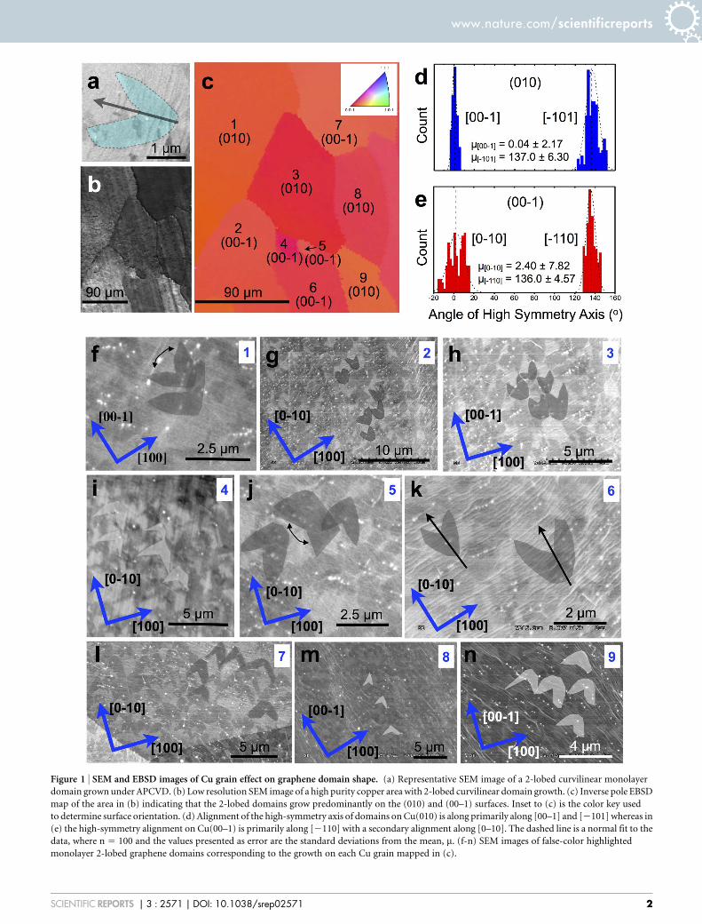
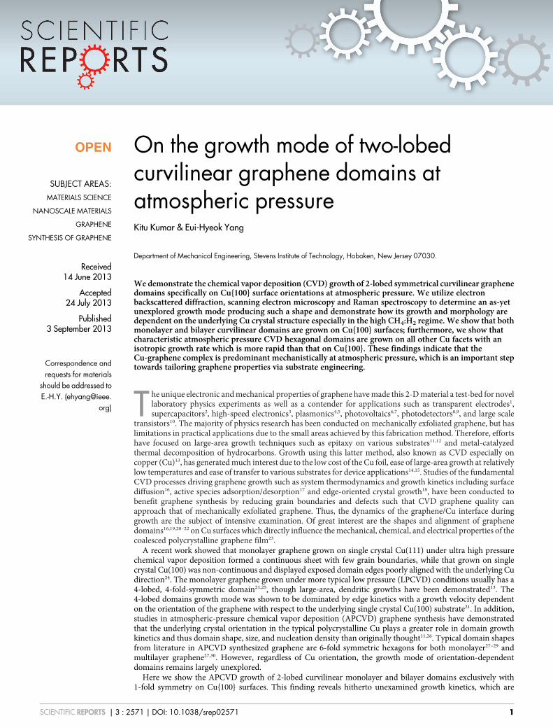
Figure 1 | SEM and EBSD images of Cu grain effect on graphene domain shape. (a) Representative SEM image of a 2-lobed curvilinear monolayer
domain grown under APCVD. (b) Low resolution SEM image of a high purity copper area with 2-lobed curvilinear domain growth. (c) Inverse pole EBSD
map of the area in (b) indicating that the 2-lobed domains grow predominantly on the (010) and (00–1) surfaces. Inset to (c) is the color key used
to determine surface orientation. (d) Alignment of the high-symmetry axis of domains on Cu(010) is along primarily along [00–1] and [2101] whereas in
(e) the high-symmetry alignment on Cu(00–1) is primarily along [2110] with a secondary alignment along [0–10]. The dashed line is a normal fit to the
data, where n 5 100 and the values presented as error are the standard deviations from the mean, m. (f-n) SEM images of false-color highlighted
monolayer 2-lobed graphene domains corresponding to the growth on each Cu grain mapped in (c).
www.nature.com/scientificreports
SCIENTIFIC REPORTS | 3 : 2571 | DOI: 10.1038/srep02571 2
modulated to a greater extent than previously reported by surfaceenergy anisotropy of Cu at atmospheric pressure. To elucidate thegrowth mode of this domain shape with respect to the Cu surface, weuse a combination of electron backscattered diffraction (EBSD),scanning electron microscopy (SEM) and Raman spectroscopy.We discuss the effects of diffusion limited growth which affects thesymmetry of these domains and also examine the angular depend-ence of the graphene axis due to surface anisotropy which controlsthe curvilinear morphology to fully determine the effect of the Culattice on growth kinetics. We show that this anisotropic growthmode is not pronounced on higher index Cu surfaces, since hexa-gonal domains are found under the same APCVD conditions onsurfaces which are not {100}. Furthermore, we experimentally showthat the anisotropic growth rate of the curvilinear domain is slowerthan the isotropic growth rate of hexagonal/polygonal domains andattribute this to strain effects from lattice mismatch. Finally, wediscuss how Cu surface energy may influence the bilayer growthmode, inducing similar growth kinetics, by straining of the inter-mediary monolayer graphene sheet.
ResultsWe investigated graphene growth under conditions chosen to elu-cidate the mechanism of anisotropic growth. Flow rates of 10 sccmmethane (CH4) and 30–70 sccm H2 in 1000 sccm Ar were main-tained during the growth phase, which was terminated after 12 s or25 s to examine individual domains before they coalesced into acontinuous film. Figure 1a provides an SEM image of an isolated2-lobed curvilinear structure after 25 s of growth. These distinctivemorphologies were grown only on the Cu{100} surfaces (Figure 1c)of high purity Cu (99.999% Alfa Aesar). The high symmetry axis ofthe domains was found to be well aligned, as shown in Figure 1d,e,along [00–1] and [2110] with secondary alignment along [2101]and [0–10], respectively. The high-symmetry axis was also found tobe well aligned to the perpendicular intersect of Cu surface steps(Figure 1k,n). On Cu{100}, domain growth was found to remainunbroken across rolling striations, surface steps, and grain bound-aries, though these surface features increased graphene nucleationdensity and played a role in morphology variation. Additionally,vicinity to other graphene domains had well-defined effects on singlelobed morphology. The growth and presence of the curvilineardomain shape under APCVD conditions is puzzling; we elucidatethe origin of this shape and growth mode below.
DiscussionLPCVD studies often produce lobed or flower-like graphene domains31
on Cu(100) orientations. In these cases, growth has been shown to belimited by angularly dependent edge kinetics, i.e., alignment of thefast growth direction of individual lobes with both the slow growthdirection and Cu orientation produces 4-lobed morphologies, suchthat the flakes formed are not single crystals21. On the other hand, inAPCVD growth, the hexagon/polygonal single crystal domain morp-hologies typically reported are limited by edge selectivity duringgrowth, wherein the carbon attachment to only armchair edges isenergetically stable, thus converting these edges to the zigzag orienta-tion32. The six-fold symmetric growths reported in these studies islargely independent of Cu surface orientation, except in one casewhere the growth temperature was reduced, thereby growing 2-foldsymmetric rectangular domains on only Cu(111)33. However, in thatstudy, the growth mechanism was not clearly elucidated.
In our study, the distinct case of curvilinear growth specifically onthe Cu{100} facets may be influenced by two causes. One is the ratioof CH4:H2 pressure which, in the case of the experiments presentedhere, is higher than typically found in literature. According toVlassiouk et al.27, at a fixed CH4 partial pressure, greater H2 partialpressures would result in a distinct hexagonal shape of domains withzigzag edges since hydrogen etching of graphene is most efficient
along this orientation27,34. In these studies, carbon concentrationsare in the parts per million, whereas our experiments have ordersof magnitude greater CH4 concentrations as described above.Therefore, we are operating in a different growth regime, and thushydrogen etching can be ruled out as the predominant mechanismfor the curvilinear shape. The second cause is more complex andinvolves several growth kinetic processes, indicating an unstudiedgrowth mode on Cu(100) at atmospheric pressure. To examine thisgrowth mode, we scrutinize the following phenomena:
1) Mobile carbon atoms at the Cu surface can diffuse along one ofthe four equivalent lattice directions of the substrate whichwould extend the domain growth along one of these directions35.Indeed, graphene has already been proven to align in two direc-tions on Cu(100) under both LPCVD and APCVD22,26,35,36
though the angle between the two directions can be smearedanywhere from 30–90u depending on the presence of stepbunches or other surface interruptions. In our work, the twofast growth axes of the curvilinear domains (Figure 2a) areseparated by a mean angle of 86.6u relative to each other(Figure 2b). Coupled with the alignment of the domain highsymmetry axes with either [00–1] or [2101] on Cu(010) andeither [2110] or [0–10] on Cu(00–1) indicates that the two fastgrowth fronts are most efficient along the ,101. (Figure 2c) or,100. directions. This efficiency is attributed to surface energyanisotropy stemming from electron density correlationsbetween the Cu lattice directions with highest atomic densityand the graphene fast growth axes26.
2) If the domain growth is diffusion limited, i.e. directly influencedby surface energy anisotropy, the observed shape of a curvilinearlobe should be well fit to the function describing the angulardependence of the fast growth velocity to surface anisotropy21.Here, the velocity of the fast growth axis depends on the relativeorientation of the graphene and Cu21. The model is describedas
v(h)~ 1zrð Þz 1{rð Þcos(h) ð1Þ
where v is the growth velocity, h is the angle between the edgenormal and slow growth direction, and r is the ratio of thevelocities in the slow and the fast directions and is the aniso-tropy factor for the 4-fold symmetric Cu(100) surface. Thepurely fast axis mean velocity was determined to be 1.13 6
0.67 (s.d.) mm/s from domain enlargement between 12 s and25 s growths (Figure 2d,e respectively). Using the well-knownanisotropy factor r 5 0.25, which predicts a sharp tipped lobeand is prevalent in our domains as seen in Figure 2a, we found aclose fit with our curvilinear shape (Supplementary Figure S1).This model demonstrates that the distinctive shape of the gra-phene lobes on Cu{100} emerges from a growth velocity whichis indeed angularly dependent on surface anisotropy. Therefore,in the regime of high CH4:H2 growth, growth is dominated bysurface diffusion and graphene orientation dependent kinetics,in sharp contrast to the reported APCVD 6-fold growth via edgeselectivity32. We attribute the presence of the 1-fold symmetrywith 2-lobes (rather than 4-lobes) to growth downhill the stepsperpendicular to the [00–1] and [2110] directions Upwardgrowth is prevented here due to the higher activation energy37
required for diffusion. We also note that as the fast growth frontapproaches adjacent domains (Figure 2e), the axis is notdeflected; rather, the slow growth velocity increases in that dir-ection. The cause of this effect is unclear, but accounts for thesubstantial variations from the mean lobe-to-lobe angle in 25 sgrowth compared to 12 s growth as in Figure 2b.
We now show that 6-fold symmetric graphene growth occurs onall other Cu surfaces measured. Figure 3 details 12 s growths onhigher index Cu facets (Figure 3a,d). Here, the domains largely
www.nature.com/scientificreports
SCIENTIFIC REPORTS | 3 : 2571 | DOI: 10.1038/srep02571 3
Figure 2 | SEM images and data on 2-lobed curvilinear monolayer domain evolution. (a) A representative 25 s growth, 2-lobed curvilinear domain on
Cu(010), with fast growth axes as indicated by white arrows. The curved black arrow represents the relative angle between the fast growth axes (lobes).
(b) Histogram of angle between the fast growth axes of the curvilinear domains on Cu{100} surfaces after 12 s and 25 s of growth with mean values of
40.9u and 86.6u, respectively. n 5 317 and the values presented as error are the standard deviations from the mean, m. (c) Image of the (010) surface as in
(a) with blue arrows denoting Cu directions, [00–1] and [2101], upon which the domains’ high symmetry axes typically align. Grey arrows indicate
direction of lobe growth, typically along [210–1] and [10–1], if the high symmetry axis is aligned to [00–1]. Evolution of domain morphology between
(d) 12 s and (e) 25 s of growth. Fast growth axes marked with white arrows. (d) Appearance of branching in the precursor to the two lobed structure is
indicated with blue arrows. Morphology change from curvilinear to hexagonal over a grain boundary is marked with blue circles. (e) Increase of slow
growth rate as the fast growth front of one domain approaches another. Based on percentage of Cu covered by the graphene domain between 12 s and 25 s
of growth, a growth velocity of 1.13 6 0.67 mm/s is calculated in the purely fast direction. Scale bars are (a) 1 mm, (d) 0.75 mm and (e) 2.5 mm.
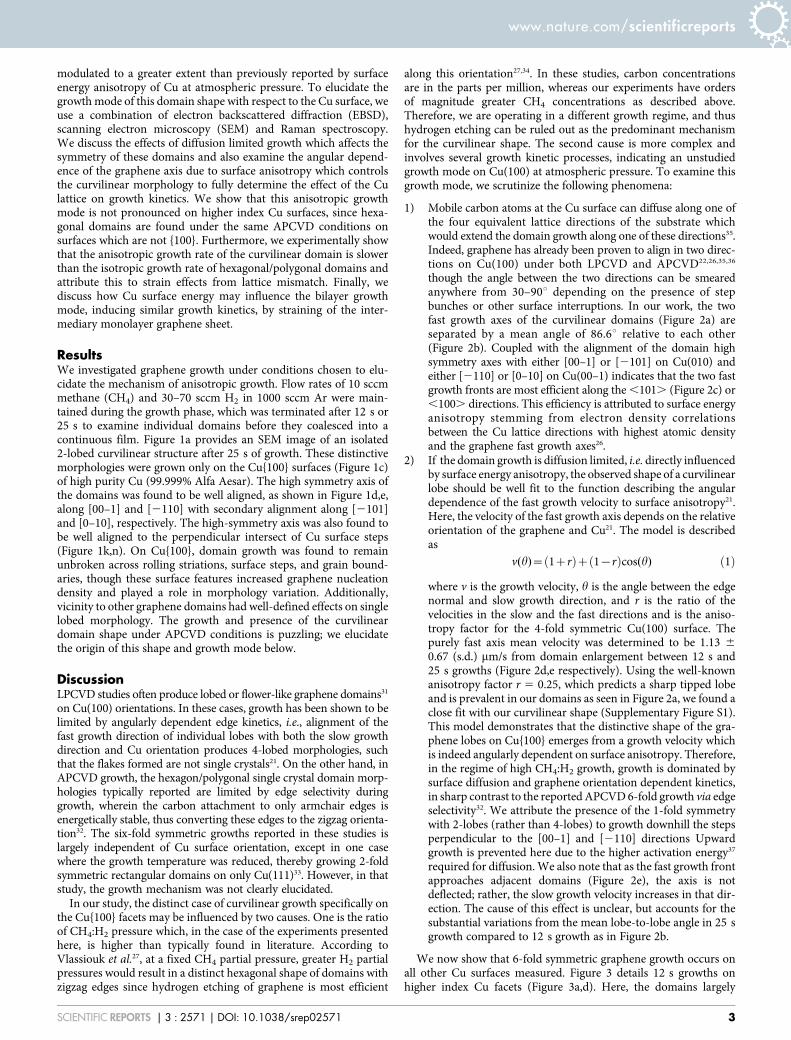
Figure 3 | Graphene domain shape dependence on Cu orientation, 12 s growth. (a), (d) Inverse pole EBSD maps of predominantly non-(100) Cu facets.
Inset to (a) is the color key used to determine surface orientation. (b), (c1-3), (e1-3) SEM images show that, under atmospheric pressure, hexagonal
domains with predominantly isotropic growth trajectories are prevalent on high-index Cu facets such as (173), (122), and (112), with no evidence of the
2-lobed domains. (c1-3) SEM images of graphene domains whose low nucleation density is dependent on carbon concentration across the surface.
(c3) Nucleation density of precursors to the 2-lobed curvilinear domain on (010) is lowest, confirming surface diffusion as the limiting factor in
curvilinear growth. (e1-3) Details of high energy nucleation sites such as rolling striations (blue highlight) and nanoparticles (red arrows). (e1) Straining
of growth trajectories due to surface steps (blue arrows) create morphological changes varying from predominantly isotropic growth domains
(cyan hexagons) to moderately strained growth (yellow polygons) to 2-fold symmetric strained growth (white rectangles).
www.nature.com/scientificreports
SCIENTIFIC REPORTS | 3 : 2571 | DOI: 10.1038/srep02571 4
nucleate on rolling-induced striations (and this density remains thesame across the Cu facets) or steps and nanoparticles27, all energet-ically favorable points which reduce the activation energy for adsorp-tion of carbon species38. However, in locations where these surfaceinterruptions do not exist, (Figure 3c,1–2), nucleation density can beassumed to be directly proportional to carbon concentration on thesurface. The low nucleation density on the high index Cu surfacesand even lower density on Cu(010), further confirms that growth issurface diffusion limited39. On higher index Cu, the edges of thegraphene domains appear to be randomly oriented. However, sub-stantial morphology change occurs from hexagonal to rectangularshape (Figure 3e,1) as growth trajectories are strained39 parallel to thesurface steps.
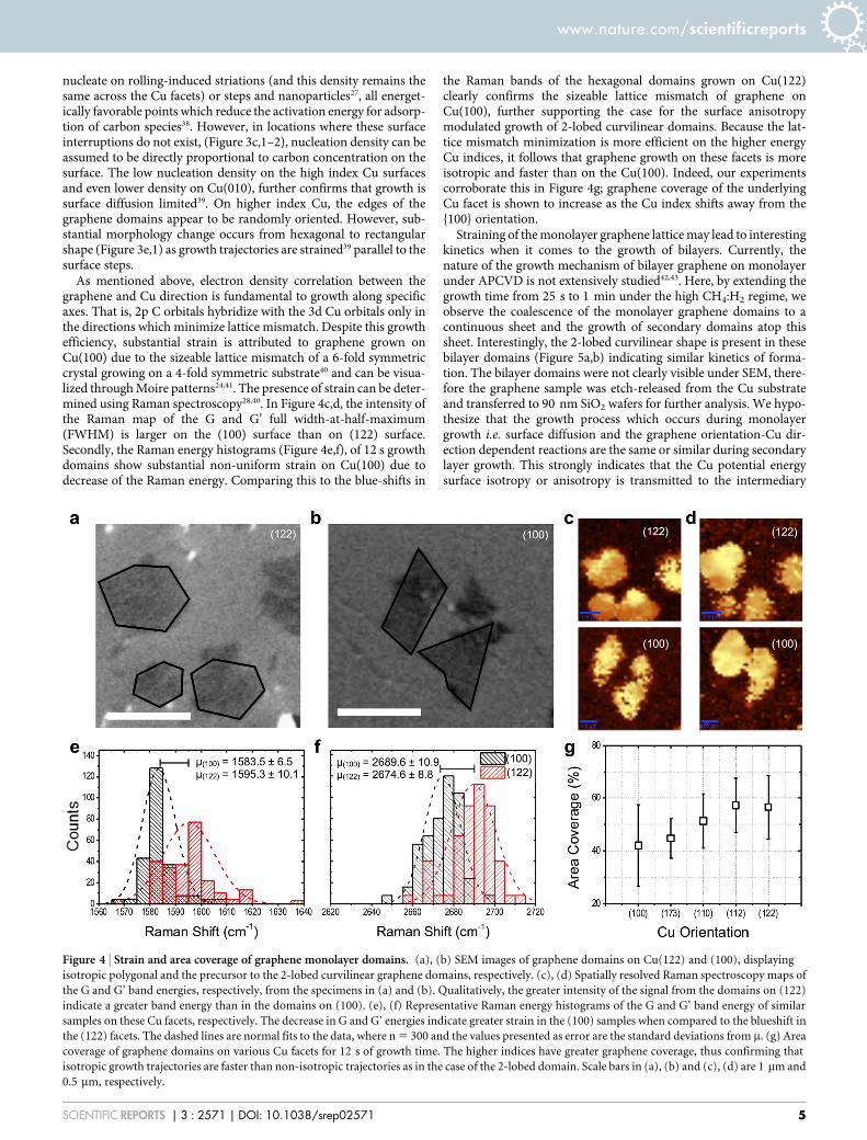
As mentioned above, electron density correlation between thegraphene and Cu direction is fundamental to growth along specificaxes. That is, 2p C orbitals hybridize with the 3d Cu orbitals only inthe directions which minimize lattice mismatch. Despite this growthefficiency, substantial strain is attributed to graphene grown onCu(100) due to the sizeable lattice mismatch of a 6-fold symmetriccrystal growing on a 4-fold symmetric substrate40 and can be visua-lized through Moire patterns24,41. The presence of strain can be deter-mined using Raman spectroscopy28,40. In Figure 4c,d, the intensity ofthe Raman map of the G and G’ full width-at-half-maximum(FWHM) is larger on the (100) surface than on (122) surface.Secondly, the Raman energy histograms (Figure 4e,f), of 12 s growthdomains show substantial non-uniform strain on Cu(100) due todecrease of the Raman energy. Comparing this to the blue-shifts in
the Raman bands of the hexagonal domains grown on Cu(122)clearly confirms the sizeable lattice mismatch of graphene onCu(100), further supporting the case for the surface anisotropymodulated growth of 2-lobed curvilinear domains. Because the lat-tice mismatch minimization is more efficient on the higher energyCu indices, it follows that graphene growth on these facets is moreisotropic and faster than on the Cu(100). Indeed, our experimentscorroborate this in Figure 4g; graphene coverage of the underlyingCu facet is shown to increase as the Cu index shifts away from the{100} orientation.
Straining of the monolayer graphene lattice may lead to interestingkinetics when it comes to the growth of bilayers. Currently, thenature of the growth mechanism of bilayer graphene on monolayerunder APCVD is not extensively studied42,43. Here, by extending thegrowth time from 25 s to 1 min under the high CH4:H2 regime, weobserve the coalescence of the monolayer graphene domains to acontinuous sheet and the growth of secondary domains atop thissheet. Interestingly, the 2-lobed curvilinear shape is present in thesebilayer domains (Figure 5a,b) indicating similar kinetics of forma-tion. The bilayer domains were not clearly visible under SEM, there-fore the graphene sample was etch-released from the Cu substrateand transferred to 90 nm SiO2 wafers for further analysis. We hypo-thesize that the growth process which occurs during monolayergrowth i.e. surface diffusion and the graphene orientation-Cu dir-ection dependent reactions are the same or similar during secondarylayer growth. This strongly indicates that the Cu potential energysurface isotropy or anisotropy is transmitted to the intermediary
Figure 4 | Strain and area coverage of graphene monolayer domains. (a), (b) SEM images of graphene domains on Cu(122) and (100), displaying
isotropic polygonal and the precursor to the 2-lobed curvilinear graphene domains, respectively. (c), (d) Spatially resolved Raman spectroscopy maps of
the G and G’ band energies, respectively, from the specimens in (a) and (b). Qualitatively, the greater intensity of the signal from the domains on (122)
indicate a greater band energy than in the domains on (100). (e), (f) Representative Raman energy histograms of the G and G’ band energy of similar
samples on these Cu facets, respectively. The decrease in G and G’ energies indicate greater strain in the (100) samples when compared to the blueshift in
the (122) facets. The dashed lines are normal fits to the data, where n 5 300 and the values presented as error are the standard deviations from m. (g) Area
coverage of graphene domains on various Cu facets for 12 s of growth time. The higher indices have greater graphene coverage, thus confirming that
isotropic growth trajectories are faster than non-isotropic trajectories as in the case of the 2-lobed domain. Scale bars in (a), (b) and (c), (d) are 1 mm and
0.5 mm, respectively.
www.nature.com/scientificreports
SCIENTIFIC REPORTS | 3 : 2571 | DOI: 10.1038/srep02571 5
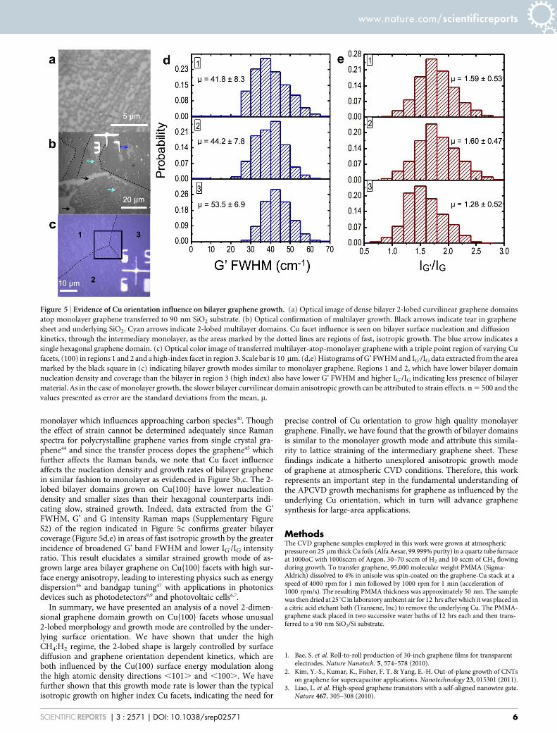
monolayer which influences approaching carbon species30. Thoughthe effect of strain cannot be determined adequately since Ramanspectra for polycrystalline graphene varies from single crystal gra-phene44 and since the transfer process dopes the graphene45 whichfurther affects the Raman bands, we note that Cu facet influenceaffects the nucleation density and growth rates of bilayer graphenein similar fashion to monolayer as evidenced in Figure 5b,c. The 2-lobed bilayer domains grown on Cu{100} have lower nucleationdensity and smaller sizes than their hexagonal counterparts indi-cating slow, strained growth. Indeed, data extracted from the G’FWHM, G’ and G intensity Raman maps (Supplementary FigureS2) of the region indicated in Figure 5c confirms greater bilayercoverage (Figure 5d,e) in areas of fast isotropic growth by the greaterincidence of broadened G’ band FWHM and lower IG’/IG intensityratio. This result elucidates a similar strained growth mode of as-grown large area bilayer graphene on Cu{100} facets with high sur-face energy anisotropy, leading to interesting physics such as energydispersion46 and bandgap tuning47 with applications in photonicsdevices such as photodetectors8,9 and photovoltaic cells6,7.
In summary, we have presented an analysis of a novel 2-dimen-sional graphene domain growth on Cu{100} facets whose unusual2-lobed morphology and growth mode are controlled by the under-lying surface orientation. We have shown that under the highCH4:H2 regime, the 2-lobed shape is largely controlled by surfacediffusion and graphene orientation dependent kinetics, which areboth influenced by the Cu(100) surface energy modulation alongthe high atomic density directions ,101. and ,100.. We havefurther shown that this growth mode rate is lower than the typicalisotropic growth on higher index Cu facets, indicating the need for
precise control of Cu orientation to grow high quality monolayergraphene. Finally, we have found that the growth of bilayer domainsis similar to the monolayer growth mode and attribute this simila-rity to lattice straining of the intermediary graphene sheet. Thesefindings indicate a hitherto unexplored anisotropic growth modeof graphene at atmospheric CVD conditions. Therefore, this workrepresents an important step in the fundamental understanding ofthe APCVD growth mechanisms for graphene as influenced by theunderlying Cu orientation, which in turn will advance graphenesynthesis for large-area applications.
MethodsThe CVD graphene samples employed in this work were grown at atmosphericpressure on 25 mm thick Cu foils (Alfa Aesar, 99.999% purity) in a quartz tube furnaceat 1000oC with 1000sccm of Argon, 30–70 sccm of H2 and 10 sccm of CH4 flowingduring growth. To transfer graphene, 95,000 molecular weight PMMA (Sigma-Aldrich) dissolved to 4% in anisole was spin-coated on the graphene-Cu stack at aspeed of 4000 rpm for 1 min followed by 1000 rpm for 1 min (acceleration of1000 rpm/s). The resulting PMMA thickness was approximately 50 nm. The samplewas then dried at 25uC in laboratory ambient air for 12 hrs after which it was placed ina citric acid etchant bath (Transene, Inc) to remove the underlying Cu. The PMMA-graphene stack placed in two successive water baths of 12 hrs each and then trans-ferred to a 90 nm SiO2/Si substrate.
1. Bae, S. et al. Roll-to-roll production of 30-inch graphene films for transparentelectrodes. Nature Nanotech. 5, 574–578 (2010).
2. Kim, Y.-S., Kumar, K., Fisher, F. T. & Yang, E.-H. Out-of-plane growth of CNTson graphene for supercapacitor applications. Nanotechnology 23, 015301 (2011).
3. Liao, L. et al. High-speed graphene transistors with a self-aligned nanowire gate.Nature 467, 305–308 (2010).
Figure 5 | Evidence of Cu orientation influence on bilayer graphene growth. (a) Optical image of dense bilayer 2-lobed curvilinear graphene domains
atop monolayer graphene transferred to 90 nm SiO2 substrate. (b) Optical confirmation of multilayer growth. Black arrows indicate tear in graphene
sheet and underlying SiO2. Cyan arrows indicate 2-lobed multilayer domains. Cu facet influence is seen on bilayer surface nucleation and diffusion
kinetics, through the intermediary monolayer, as the areas marked by the dotted lines are regions of fast, isotropic growth. The blue arrow indicates a
single hexagonal graphene domain. (c) Optical color image of transferred multilayer-atop-monolayer graphene with a triple point region of varying Cu
facets, (100) in regions 1 and 2 and a high-index facet in region 3. Scale bar is 10 mm. (d,e) Histograms of G’ FWHM and IG’/IG data extracted from the area
marked by the black square in (c) indicating bilayer growth modes similar to monolayer graphene. Regions 1 and 2, which have lower bilayer domain
nucleation density and coverage than the bilayer in region 3 (high index) also have lower G’ FWHM and higher IG’/IG indicating less presence of bilayer
material. As in the case of monolayer growth, the slower bilayer curvilinear domain anisotropic growth can be attributed to strain effects. n 5 500 and the
values presented as error are the standard deviations from the mean, m.
www.nature.com/scientificreports
SCIENTIFIC REPORTS | 3 : 2571 | DOI: 10.1038/srep02571 6
4. Wang, P. et al. Giant optical response from graphene–plasmonic system. ACSNano 6, 6244–6249 (2012).
5. Echtermeyer, T. J. et al. Strong plasmonic enhancement of photovoltage ingraphene. Nat. Commun. 2, 458 (2011).
6. Gomez De Arco, L. et al. Continuous, highly flexible, and transparent graphenefilms by chemical vapor deposition for organic photovoltaics. ACS Nano 4,2865–2873 (2010).
7. Lee, Y.-Y. et al. Top laminated graphene electrode in a semitransparent polymersolar cell by simultaneous thermal annealing/releasing method. ACS Nano 5,6564–6570 (2011).
8. Bao, Q. & Loh, K. P. Graphene photonics, plasmonics, and broadbandoptoelectronic devices. ACS Nano 6, 3677–3694 (2012).
9. Withers, F., Bointon, T. H., Craciun, M. F. & Russo, S. All-graphenephotodetectors. ACS Nano 7, 5052–5057 (2013).
10. Petrone, N. et al. Chemical vapor deposition-derived graphene with electricalperformance of exfoliated graphene. Nano Lett. 12, 2751–2756 (2012).
11. Sutter, P. W., Flege, J.-I. & Sutter, E. A. Epitaxial graphene on ruthenium. NatureMater. 7, 406–411 (2008).
12. Berger, C. Electronic confinement and coherence in patterned epitaxial graphene.Science 312, 1191–1196 (2006).
13. Li, X. et al. Large-area graphene single crystals grown by low-pressure chemicalvapor deposition of methane on copper. J. Am. Chem. Soc. 133, 2816–2819 (2011).
14. Suk, J. W. et al. Transfer of CVD-grown monolayer graphene onto arbitrarysubstrates. ACS Nano 5, 6916–6924 (2011).
15. Li, X. et al. Transfer of large-area graphene films for high-performancetransparent conductive electrodes. Nano Lett. 9, 4359–4363 (2009).
16. Bhaviripudi, S., Jia, X., Dresselhaus, M. S. & Kong, J. Role of kinetic factors inchemical vapor deposition synthesis of uniform large area graphene using coppercatalyst. Nano Lett. 10, 4128–4133 (2010).
17. Kim, H. et al. Activation energy paths for graphene nucleation and growth on Cu.ACS Nano 6, 3614–3623 (2012).
18. Wu, B. et al. Equiangular hexagon-shape-controlled synthesis of graphene oncopper surface. Adv. Mater. 23, 3522–3525 (2011).
19. Li, X. et al. Graphene films with large domain size by a two-step chemical vapordeposition process. Nano Lett. 10, 4328–4334 (2010).
20. Gao, L., Guest, J. R. & Guisinger, N. P. Epitaxial graphene on Cu(111). Nano Lett.10, 3512–3516 (2010).
21. Wofford, J. M., Nie, S., McCarty, K. F., Bartelt, N. C. & Dubon, O. D. Grapheneislands on Cu foils: the interplay between shape, orientation, and defects. NanoLett. 10, 4890–4896 (2010).
22. Nie, S., Wofford, J., Bartelt, N., Dubon, O. & McCarty, K. Origin of the mosaicityin graphene grown on Cu(111). Phys. Rev. B 84, 155425 (2011).
23. Novoselov, K. et al. A roadmap for graphene. Nature 490, 192–200 (2012).24. Zhao, L. et al. Influence of copper crystal surface on the CVD growth of large area
monolayer graphene. Solid State Commun. 151, 509–513 (2011).25. Li, X., Cai, W., Colombo, L. & Ruoff, R. S. Evolution of graphene growth on Ni and
Cu by carbon isotope labeling. Nano Lett. 9, 4268–4272 (2009).26. Murdock, A. T. et al. Controlling the orientation, edge geometry, and thickness of
chemical vapor deposition graphene. ACS Nano 7, 1351–1359 (2013).27. Vlassiouk, I. et al. Role of hydrogen in chemical vapor deposition growth of large
single-crystal graphene. ACS Nano 5, 6069–6076 (2011).28. Yu, Q. et al. Control and characterization of individual grains and grain
boundaries in graphene grown by chemical vapour deposition. Nature Mater. 10,443–449 (2011).
29. Huang, P. Y. et al. Grains and grain boundaries in single-layer graphene atomicpatchwork quilts. Nature 469, 389–392 (2011).
30. Robertson, A. W. & Warner, J. H. Hexagonal single crystal domains of few-layergraphene on copper foils. Nano Lett. 11, 1182–1189 (2011).
31. Li, X. et al. Large-area synthesis of high-quality and uniform graphene films oncopper foils. Science 324, 1312–1314 (2009).
32. Luo, Z., Kim, S., Kawamoto, N., Rappe, A. M. & Johnson, A. T. C. Growthmechanism of hexagonal-shape graphene flakes with zigzag edges. ACS Nano 5,9154–9160 (2011).
33. Wu, Y. A., Robertson, A. W., Schaffel, F., Speller, S. C. & Warner, J. H. Alignedrectangular few-layer graphene domains on copper surfaces. Chem. Mater. 23,4543–4547 (2011).
34. Zhang, Y., Li, Z., Kim, P., Zhang, L. & Zhou, C. Anisotropic hydrogen etching ofchemical vapor deposited graphene. ACS Nano 6, 126–132 (2012).
35. Rasool, H. I. et al. Atomic-scale characterization of graphene grown on copper(100) single crystals. J. Am. Chem. Soc. 133, 12536–12543 (2011).
36. Ogawa, Y. et al. Domain structure and boundary in single-layer graphene grownon Cu(111) and Cu(100) films. J. Phys. Chem. Lett. 3, 219–226 (2012).
37. Rasool, H. I. et al. Continuity of graphene on polycrystalline copper. Nano Lett. 11,251–256 (2011).
38. Han, G. H. et al. Influence of copper morphology in forming nucleation seeds forgraphene growth. Nano Lett. 11, 4144–4148 (2011).
39. Celebi, K. et al. Evolutionary kinetics of graphene formation on copper. Nano Lett.13, 967–974 (2013).
40. He, R. et al. Large physisorption strain in chemical vapor deposition of grapheneon copper substrates. Nano Lett. 12, 2408–2413 (2012).
41. Cho, J. et al. Atomic-scale investigation of graphene grown on Cu foil and theeffects of thermal annealing. ACS Nano 5, 3607–3613 (2011).
42. Liu, L. et al. High-yield chemical vapor deposition growth of high-quality large-area AB-stacked bilayer graphene. ACS Nano 6, 8241–8249 (2012).
43. Liu, W., Li, H., Xu, C., Khatami, Y. & Banerjee, K. Synthesis of high-qualitymonolayer and bilayer graphene on copper using chemical vapor deposition.Carbon 49, 4122–4130 (2011).
44. Bissett, M. A., Izumida, W., Saito, R. & Ago, H. Effect of domain boundaries on theraman spectra of mechanically strained graphene. ACS Nano 6, 10229–10238(2012).
45. Cheng, Z. et al. Toward intrinsic graphene surfaces: a systematic study on thermalannealing and wet-chemical treatment of SiO2-supported graphene devices. NanoLett. 11, 767–771 (2011).
46. Wong, J.-H., Wu, B.-R. & Lin, M.-F. Strain effect on the electronic properties ofsingle layer and bilayer graphene. J. Phys. Chem. C 116, 8271–8277 (2012).
47. Choi, D. et al. Fully rollable transparent nanogenerators based on grapheneelectrodes. Adv. Mater. 22, 2187–2192 (2010).
AcknowledgementsThe authors thank S. Strauf for use of his Raman spectroscopy and transmissionmeasurement systems and J. Ding, A. Moy, and S. Brew for helpful comments. EBSDcharacterization was carried out at Lehigh University, Materials Science Department.Raman spectroscopy was carried out at the Center for Functional Nanomaterials,Brookhaven National Laboratory, which is supported by the U.S. Department of Energy,Office of Basic Energy Sciences, under Contract No. DE-AC02-98CH10886. This work wassupported in part by the Robert Crooks Stanley Fellowship and National ScienceFoundation GK12 Fellowship at Stevens Institute of Technology. This work has also beensupported in part by National Science Foundation (DMR-0922522, EECS-1040007,ECCS-1104870, and EEC-1138244) and Air Force Office for Scientific Research(FA9550-11-1-0272, FA9550-12-1-0326).
Author contributionsK.K. designed and carried out the experiments, performed data analysis and wrote themanuscript. K.K. and E.H.Y. discussed the results, reviewed the manuscript, and have givenapproval to the final version of the manuscript.
Additional informationSupplementary information accompanies this paper at http://www.nature.com/scientificreports
Competing financial interests: The authors declare no competing financial interests.
How to cite this article: Kumar, K. & Yang, E.-H. On the growth mode of two-lobedcurvilinear graphene domains at atmospheric pressure. Sci. Rep. 3, 2571; DOI:10.1038/srep02571 (2013).
This work is licensed under a Creative Commons Attribution 3.0 Unported license.To view a copy of this license, visit http://creativecommons.org/licenses/by/3.0
www.nature.com/scientificreports
SCIENTIFIC REPORTS | 3 : 2571 | DOI: 10.1038/srep02571 7

![Genetic mapping of a lobed-leaf gene associated …...leaf [1,17,18]. Some molecular markers linked to lobed-leaf genes were identified. For example, a SCAR marker linked to the lobed-leaf](https://static.fdocuments.in/doc/165x107/5e771cd79b545f444838ff7a/genetic-mapping-of-a-lobed-leaf-gene-associated-leaf-11718-some-molecular.jpg)