On the Design of a 3D Network-on-Chip for Many-core SoC
74
A thesis submitted in partial satisfaction of the requirements for the degree of Master of Computer Science and Engineering in the Graduate School of the University of Aizu On the Design of a 3D Network-on-Chip for Many-core SoC by m5141153 Akram Ben Ahmed February 2012
Transcript of On the Design of a 3D Network-on-Chip for Many-core SoC

A thesis submitted in partial satisfaction of the
requirements for the degree of
Master of Computer Science and Engineering
in the Graduate School of the
University of Aizu
On the Design of a 3D Network-on-Chip
for Many-core SoC
by
m5141153
Akram Ben Ahmed
February 2012

The thesis titled
On the Design of a 3D Network-on-Chipfor Many-core SoC
by
m5141153Akram Ben Ahmed
is reviewed and approved by:
Main referee
Associate Professor Date
Ben Abdallah Abderazek
Professor Date
Kenichi Kuroda
Associate Professor Date
Mohamed Hamada
The University of Aizu
February 2012

Contents
Chapter 1 Introduction 1
1.1 Background . . . . . . . . . . . . . . . . . . . . . . . . . . . . . . . 1
1.2 Problems and Motivation . . . . . . . . . . . . . . . . . . . . . . . . 2
1.3 Thesis organization . . . . . . . . . . . . . . . . . . . . . . . . . . . 6
Chapter 2 Related Works 7
2.1 3D-NoC versus 2D-NoC . . . . . . . . . . . . . . . . . . . . . . . . 7
2.2 3D-NoC router architecture . . . . . . . . . . . . . . . . . . . . . . . 8
2.3 3D-NoC routing algorithms . . . . . . . . . . . . . . . . . . . . . . . 9
Chapter 3 Look Ahead XYZ routing algorithm 13
Chapter 4 3D-ONoC System Architecture 19
4.1 Topology . . . . . . . . . . . . . . . . . . . . . . . . . . . . . . . . 19
4.2 Switching policy . . . . . . . . . . . . . . . . . . . . . . . . . . . . 21
4.3 Router architecture . . . . . . . . . . . . . . . . . . . . . . . . . . . 22
4.3.1 Input Port . . . . . . . . . . . . . . . . . . . . . . . . . . . . 25
4.3.2 Switch Allocator . . . . . . . . . . . . . . . . . . . . . . . . 28
4.3.3 Crossbar . . . . . . . . . . . . . . . . . . . . . . . . . . . . 33
iii

4.4 Network interface . . . . . . . . . . . . . . . . . . . . . . . . . . . . 34
Chapter 5 Evaluation 39
5.1 Evaluation methodology . . . . . . . . . . . . . . . . . . . . . . . . 39
5.1.1 JPEG encoder . . . . . . . . . . . . . . . . . . . . . . . . . . 39
5.1.2 Matrix multiplication . . . . . . . . . . . . . . . . . . . . . . 42
5.2 Evaluation results . . . . . . . . . . . . . . . . . . . . . . . . . . . . 46
5.2.1 Hardware complexity evaluation . . . . . . . . . . . . . . . . 46
5.2.2 Performance analysis evaluation . . . . . . . . . . . . . . . . 48
Chapter 6 Conclusion and Future Work 56
iv

List of Figures
Figure 1.1 SoC architecture: (a) Shred-bus (b) Point-2-Point (c) NoC . . . 2
Figure 3.1 Router pipeline stages: (a) conventional XYZ (b) LA-XYZ (c)
LA-XYZ with no-load bypass. . . . . . . . . . . . . . . . . . . . . . 14
Figure 3.2 LA-XYZ routing algorithm Flow-chart. . . . . . . . . . . . . 16
Figure 4.1 Configuration example of a 4x4x4 3D-ONoC mesh topology. . 20
Figure 4.2 3D-ONOC flit format. . . . . . . . . . . . . . . . . . . . . . . 22
Figure 4.3 3D-ONoC pipeline stages: Buffer writing (BW), Routing Cal-
culation and Switch Allocation (RC/SA) and Crossbar Traversal stage
(CT). . . . . . . . . . . . . . . . . . . . . . . . . . . . . . . . . . . . 23
Figure 4.4 Verilog HDL top module of the router. . . . . . . . . . . . . . 24
Figure 4.5 Input-port module architecture. . . . . . . . . . . . . . . . . . 25
Figure 4.6 Verilog HDL implemntation of LA-XYZ routing algorithm. . . 27
Figure 4.7 Switch allocator circuit. . . . . . . . . . . . . . . . . . . . . . 28
Figure 4.8 Stall-Go flow control mechanism. . . . . . . . . . . . . . . . . 30
Figure 4.9 Stall-Go flow control: (a) State machine (b) Verilog HDL of the
state machine decision. . . . . . . . . . . . . . . . . . . . . . . . . . 31
Figure 4.10 Scheduling-Matrix priority assignment. . . . . . . . . . . . . . 33
v

Figure 4.11 Crossbar circuit. . . . . . . . . . . . . . . . . . . . . . . . . . 34
Figure 4.12 Network Interface Architecture: (a) Transmitter (b) Receiver . 35
Figure 4.13 Chip floor plan for a 2x2x2 3D-ONoC. . . . . . . . . . . . . . 37
Figure 4.14 RTL view of 2x2x2 3D-ONoC. . . . . . . . . . . . . . . . . . 38
Figure 5.1 Task graph of the JPEG encoder . . . . . . . . . . . . . . . . 40
Figure 5.2 Extended task graph of the JPEG encoder . . . . . . . . . . . 41
Figure 5.3 JPEG encoder mapped onto: (a) 2x4 2D-ONoC (b) 2x2x2 3D-
ONoC . . . . . . . . . . . . . . . . . . . . . . . . . . . . . . . . . . 42
Figure 5.4 Matrix multiplication example: The multiplication of an ixk
matrix A by a kxj matrix B results in an ixj matrix R. . . . . . . . . . 42
Figure 5.5 Simple example demonstrating the Matrix multiplication calcu-
lation. . . . . . . . . . . . . . . . . . . . . . . . . . . . . . . . . . . 43
Figure 5.6 3x3 matrix multiplication using (a) optimistic and (b) pessimistic
mapping approaches . . . . . . . . . . . . . . . . . . . . . . . . . . 45
Figure 5.7 Execution time comparison between 3D and 2D ONoC. . . . . 49
Figure 5.8 Average number of hops comparison for both pessimistic and
optimistic mapping: (a) 3x3 (b) 4x4 (c) 6x6. . . . . . . . . . . . . . . 51
Figure 5.9 Stall average count comparison between 3D and 2D ONoC. . . 52
Figure 5.10 Stall average count comparison between 3D and 2D ONoC with
different traffic loads. . . . . . . . . . . . . . . . . . . . . . . . . . . 53
Figure 5.11 Execution time comparison between 3D and 2D ONoC with
different traffic loads. . . . . . . . . . . . . . . . . . . . . . . . . . . 54
vi

List of Tables
Table 5.1 Simulation parameters. . . . . . . . . . . . . . . . . . . . . . . 47
Table 5.2 3D-ONoC hardware complexity compared with 2D-ONoC. . . . 48
vii

Acknowledgement
I want to express my thanks and gratitude to Prof. Ben Abdallah Abderazek for his
support, encouragement and his efforts and guidance to achieve this project. Also I
would like to thank both of Prof. Kenichi Kuroda and Prof. Mohamed Hamada of
the University of Aizu for taking the time to revise my thesis. Moreover, my sincere
gratitude to Dr. Kenichi Kuroda, Prof. Yuichi Okuyama, and Prof. Junji Kitamichi for
their help and support during the past two years.
Finally, I want to thank all the members of the Adaptive Systems Laboratory at the
University of Aizu, my friends and family. Their supportive words and encouraging
messages kept me motivated to work harder and be a better researcher and person .
viii

Abstract
Global interconnects are becoming the principal performance bottleneck for high
performance Systems-on-Chip (SoCs). Since the main purpose for this system is to
shrink the size of the chip as smaller as possible while seeking at the same time for
more scalability, higher bandwidth and lower latency. Conventional bus-based-systems
are no longer reliable architecture for SoC due to a lack of scalability and parallelism
integration, high latency and power dissipation, and low throughput. During this last
decade, Network-on-Chip (NoC) has been proposed as a promising solution for future
systems on chip design. It offers more scalability than the shared-bus based intercon-
nection, allows more processors to operate concurrently.
Despite the higher scalability and parallelism integration offered by the Network-
on-Chip (NoC) over the traditional shared-bus based systems, it’s still not an ideal
solution for future large scale Systems-on-Chip (SoCs), due to some limitations such
as high power consumption, high cost communication, and low throughput. Recently,
merging NoC to the third dimension (3D-Noc) has been proposed to deal with those
problems, as it was a solution offering lower power consumption and higher speed.
In this this thesis, a 3D-NoC named OASIS (in short 3D-ONoC) has been designed
to overcome the limitations of 2D-OASIS previously made in our research group. In
this dissertation we describe the 3D OASIS-NoC architecture in a fair amount of detail
and present evaluation results and comparison between 3D and 2D OASIS.
Evaluation results show that despite the increasing hardware complexity, 3D ONoC
reduces the number of hops by 40% and also the average stall count by 74%. As a result
the execution time improved by 36%. By increasing the traffic load with the Matrix

application, the execution time could be further enhanced from 36% obtained with one
matrix multiplication to more than 41% with 1, 2, 3 and 4 matrix multiplications.
x

Chapter 1
Introduction
1.1 Background
Following Moore’s law, the number of transistors kept increasing along the past
few decades. That made shrinking the chip size while maintaining high performance
possible. This technology scaling has allowed Systems-on-Chip (SoCs) [1, 2] systems
to grow continuously in component count and complexity. Which significantly led to
some very challenging problems such us power dissipation, resource management etc.
In particular, the interconnection network starts to play a more and more important
role in determining the performance and also the power consumption of the entire chip
[3]. Those factors made conventional bus-based-systems and P2P no longer reliable
architectures for SoC, due to the lack of scalability and parallelism integration, high
latency and power dissipation, and low throughput.
Network-on-Chip [1, 4] was introduced as a promising method that can respond
to these issues. Based on a simple and scalable architecture platform, NoC connects
processors, memories and other custom designs together using switching packets on
a hop-by-hop basis, in order to provide a higher bandwidth and higher performance.
Figure1.1 (a) and Fig.1.1 (b) show one of the most well-known architectures which
1

(a) (b)
(c)
Figure 1.1: SoC architecture: (a) Shred-bus (b) Point-2-Point (c) NoC
are respectively Point-to-Point (P2P) and shared bus systems. As shown in Fig.1.1 (c),
NoC architectures are based upon connecting segment (or wires) and switching blocks
to combine the benefits of the two previous architectures while reducing their disad-
vantages, such us the large numbers of long wires in P2P and the lack of scalability in
shared-bus systems.
1.2 Problems and Motivation
At the same time, future applications are getting more and more complex, demand-
ing a good architecture to ensure a sufficient bandwidth for any transaction between
2

memories and cores as well as communication between different cores on the same
chip. All this factors made NoC not enough reliable for future systems, especially
when we talk about hundreds of cores. This limitation comes basically from the high
diameter that suffers from NoC. The network’s diameter is the number of hops that a
flit traverses in the longest possible minimal path between a (source, destination) pair.
The diameter is important for the NoC design since a large network diameter has a neg-
ative impact on the worst case routing latency in the network. For all these facts, the
seek for optimizing NoC-based architecture becomes more and more necessary, and
many researches have been conducted to achieve this goal in various approaches, such
as developing fast routers [5, 6, 7, 8] or designing new network topologies [9, 10, 11].
One of these proposed solutions was merging the Network-on-Chip to the third
dimension. In the past few years, three dimensional integrated circuits (3D-ICs) [12]
have attracted a lot of attention as a potential solution to resolve the interconnect bottle-
neck. A three dimensional chip is a stack of multiple device layers with direct vertical
interconnects tunneling through them [13, 14]. Researches made so far have shown that
3D-ICs can achieve higher packing density due to the addition of a third dimension to
the conventional two-dimensional layout; and thanks to the reduced average intercon-
nect length, 3D-ICs can achieve higher performance. Besides that, this reduction of
total wiring, a lower interconnect power consumption can be obtained [15, 16], not
forget to mention that circuitry is more immune to noise with 3D-ICs [12]. This may
offer an opportunity to continue performance improvements using CMOS technology
with smaller form factors, higher integration densities and supporting the realization
3

of mixed-technology chips [17]. As Topol et al in [16] stated, 3D-IC can improve the
performance even in absence of scalability. Combining the NoC structure with the
benefits of the 3D integration leads us to present 3D-NoC as a new architecture. This
architecture responds to the scaling demands for future SoC, exploiting the short verti-
cal links between the adjacent layers that can clearly enhance the system performance.
This combination may provide a new horizon NoC design to satisfy the high require-
ments of future large scale applications.
One of the important design steps that should be taken care of while designing an
3D-NoC is to implement an efficient router, as it is the backbone of any NoC archi-
tecture. The router performance depends on many factors and techniques, such as the
traffic pattern, the router pipeline design and the network topology. As Feihui et al
in [18] mentioned, among these three factors we have less control over the traffic pat-
terns compared with the topology and the pipeline design. Following this logic, and
assuming the topology choice was already taken, one of the most important router en-
hancements that can be done is to improve the pipeline design, and then reducing the
router delay. By reducing the pipeline delay, not only we decrease the per-hop delay,
but also the whole network latency will be reduced.
On the other hand, the pipeline design is strongly associated with the routing al-
gorithm adopted by the design. Routing is the process of determining the path that
a flit should take between one source and one destination node. Routing algorithm
can classified into minimal or non-minimal, depending on whether flits traveling from
source to destination always use the minimal possible path or not. Minimal routing
4

schemes are shorter and require less complex hardware, but allowing non-minimal
routes increases the path diversity and decreases the network congestion. Also the
routing algorithms can be adaptive, where routing decisions are made based on the
network congestion status and other information about network links or buffer occu-
pancy of the neighboring nodes, or alternatively are deterministic. Although there are a
large number of sophisticated adaptive routing algorithms, but they could require more
complex implementation than that of the deterministic ones. That’s why deterministic
routing schemes has been adopted for 3D-NoC designs. One of the well-known and
well used routing schemes used in 3D-NoCs is the Dimension Order Routing (DOR)
XYZ algorithm. XYZ is a simple scheme, easy to implement and free of deadlock and
lifelock. But on the other hand, it suffers from a non-efficient pipeline stage usage.
This can introduce an additional packet latency which has an important effect on the
router delay and eventually on the system overall performance. Enhancing this algo-
rithm while keeping its simplicity may improve the system performance by reducing
the packet delay.
Previously, in our research group, we proposed a 2D-NoC named OASIS [4, 19,
20]. Although 2D-OASIS-NoC has its advantages over the shared-bus based systems,
it has also some limitations such as high power consumption, high cost communication,
and low throughput.
Starting from all these facts, the main motivation of this work is to propose a
3D-NoC named 3D-OASIS-NoC which is an extension to our 2D-OASIS-NoC. 3D-
OASIS-NoC uses our proposed efficient routing scheme named Look-ahead-XYZ (LA-
XYZ). This algorithm improves the router pipeline design by parallelizing some stages
5

while taking advantage at the same time of the simplicity of the conventional XYZ. As
a result, this routing scheme aims to enhance the router performance thereby achieving
a low-latency design.
In this thesis, we present a complete architecture and design of 3D-OASIS-NoC in
a fair amount of details. Evaluation results are also presented using real applications
(JPEG encoder and Matrix Multiplication). We provide more details about the differ-
ent components of 3D-OASIS-NoC including our proposed Look-ahead-XYZ routing
scheme (LA-XYZ) and its ability to optimize the router pipeline design. We show how
our design can present a better performance by reducing the congestion, decreasing
the execution time and the power consumption when compared with the previously
designed 2D-OASIS-NoC system.
1.3 Thesis organization
The rest of this dissertation is organized as follow: In Chapter 2, we present some
related works. Our proposed Look-ahead-XYZ routing algorithm (LA-XYZ) is de-
scribed in Chapter 3, and then the architecture of the 3D-OASIS-NoC system is de-
scribed in details in Chapter 4. Chapter 5 presents evaluation methodology and results.
Finally, we end the paper with concluding remarks and future works in Chapter 6.
6

Chapter 2
Related Works
In this chapter, we present some of the related works to 3D-NoC. Starting from
those who focused on the benefits of 3D-NoC when compared with 2D designs, pass-
ing by those who investigated about the router architecture and routing algorithms
dedicated for 3D-NoC.
2.1 3D-NoC versus 2D-NoC
3D-NoC is a widely studied research topic, and many related works have been
conducted until now. Few of them focused on the benefits of the 3D-NoC architecture
over the traditional 2D-NoC design. Feero et al [21] showed that 3D-NoC has the
ability to reduce latency and the energy per packet by decreasing the number of hopes
by 40% which is a basic and important factor to evaluate the system performance [21].
Pavlidis et al [22] analyzed the zero-load latency and power consumption, and
demonstrated that a decrease of 62% and 58% in power consumption can be achieved
with 3D-NoC when compared to a traditional 2D-NoC topology for a network size of
N= 128 and N= 256 nodes, respectively, where N is the number of cores connected in
the network. This power consumption reduction can simply be related to the reduction
of number of hops, since a flit has less hops to traverse to go from one source to its
7

destination, and that includes less buffer access, less switch arbitration, and less link
and crossbar traversal. All of these factors will eventually lead to decrease the power
consumption.
2.2 3D-NoC router architecture
Another part of the researches focused on the router architecture. For example, Li
et al [23] has modified the conventional 7x7 3D router using a shared bus as a commu-
nication interface between the different layers of the router, to create a 3D NoC-Bus
Hybrid router. This kind of routers reduces in fact the number of ports in each router
from 7 to 6, but on the other hand flits wishing to travel from one layer to another
should compete the access to the shared bus, since it’s the only inter-layer communica-
tion interface. This may lead to undesirable performance degradation especially under
a heavy inter-layer traffic.
Yan et al [24], also proposed another architecture for the the 3D-router, by imple-
menting all the vertical links into a single 3D-crossbar. In this case, the router has only
5 ports since we dont need any more additional ports for the vertical connections. This
technique reduces the inter-layer distance, and makes the travel between the different
layers in one single hop possible. But this router also engenders a high router cost
besides the implementation complexity of such router, which cannot be acceptable for
some simple application that actually does not need such a complex router.
For all these facts, we adopted for our design, as most of the 3D-NoC designs use,
the conventional 7x7 3D-router, as it is the lowest cost among the other architectures
and also the simplest to implement showing several properties like regularity, concur-
8

rent data transmission, and controlled electrical parameters [25, 26]. All the benefits
are acquired while making sure that this low cost and simple implementation does not
affect the performance of our system.
2.3 3D-NoC routing algorithms
Many routing algorithms have been proposed for MPSoC networks but most of
them focus only on 2D-network topologies. Among all the studies conducted for 3D-
NoC few of them focused on routing algorithms. Between the few proposed ones,
there are some custom routing schemes that aims to reduce the power consumption
and thermal power which is a very challenge design for 3D-NoC systems. For instance,
Ramanujam et al [27] presented an oblivious routing algorithm called randomized par-
tially minimal (RPM) that aims to load balance the traffic along the network improving
then the worst case scenario. RPM sends packets to a random layer first, then route
them along their X and Y dimensions using either XY or YX routing with equal prob-
ability. Finally packets are sent to their final destination along the Z dimension.
In a quiet similar technique, Chao et al [28] addressed the thermal power problem
in 3D-NoC, which is one of the most important issues in the 3D-NoC designs. Starting
from the fact the upper layer in the network detains the highest thermal power in the
design, they proposed a thermal aware downward routing scheme that sends first the
traffic to a downer layer, routes along the X and Y dimension before sending the pack-
ets back up to their destination layer. This technique avoids communication in upper
layers, where the thermal power is more important than the downer ones, and then may
reduce the overall thermal power in the design. Thus, ensuring thermal safety while
9

guaranteeing less performance impact from temperature regulation.
Both of these two routing algorithms have their advantages in term of load balanc-
ing and thermal power reduction. But the routing used is not minimal, which effect in
a direct way the number of hops. By adopting a non-minimal routing, the packet delay
may increase in the system, especially when we talk about a large number of connected
nodes.
To ensure a minimal path for flits when traveling the network while making the
routing as simple as possible, the majority of the remaining 3D-NoC systems have
been using the conventional minimal Dimension Order Routing (DOR) XYZ routing
scheme. Other introduced a routing scheme based upon XYZ such as the case of Tyagi
in [29] who extended a previous routing algorithm [30] called BDOR designated for
2D-NoC. BDOR forwards packets in one of two routes (XY- or YX-orders), depending
on relative position of a source-destination pair, and that aims to improve the balance
of paths along the network also when taking into account the destination.
XYZ routing scheme, and all the routing algorithms based upon it, is presented as a
vertically balanced routing algorithm which has the best performance, since it’s simple
to implement, it is free of deadlock and lifelock, and also because packet ordering is
not required [28, 31, 32]. On the other hand, it cannot always make the best use of
each pipeline stage. For the simple reason that since the Switch Allocation stage (SA)
is always dependent on the previous Routing Calculation (RC) one. This dependency
can be explained by the fact that SA stage needs information about the desired output-
port calculated from the RC stage, where the incoming flits should go through in order
to pass to the next neighboring node. To solve this problem in 2D-NoC systems using
10

the Dimension Order Routing (DOR) XY routing scheme, a smart pipeline design
can be adopted with the help of some advanced techniques like look-ahead routing
[29]. This kind of routing has been used to reduce the pipeline stages in the router, by
parallelizing some of these stages then reducing the router delay and then enhancing
the system performance. Look-ahead routing has indeed been used with 2D-NoC but
it hasn’t been adopted for 3D Network-on-Chip architectures before.
A second problem that can be seen with a lot of conventional router using XYZ-
based routing schemes, is in case of no-load traffic and when the input buffer is empty,
the flit entering the router should be first stored in the input buffer before advancing
the next RC stage even there is no any flit under process in the next stages. This un-
necessary stall will increase the packet latency in the router, and its associated power
consumption, adding a performance overhead to the whole system even in a light traf-
fic case where the system is supposed to have a close-to-optimal performance since
there is no congestion that may increase the latency. In order to face this problem, a
technique called no-load bypass is used [33]. This technique allows the flit to advance
to the RC stage in case where the buffer is empty. Then overlapping the unnecessary
buffer writing stage (BW) then decreasing the router delay.
Previously in [34], a part of this research has been including architecture of a
3D Network-on-Chip architecture (named 3D-OASIS-NoC) based on a previously de-
signed 2D-OASIS-NoC. The design’s performance was evaluated using a simple ap-
plication that randomly generates flits and sends them along the network. But real
application could not be evaluated due to the absence of some components in the de-
sign such us the network interface. For that reason, a network interface has been added
11

to 3D-ONoC, the optimized version of 3D-OASIS-NoC, in order to make our system
able to be evaluated with our real selected target applications (JPEG encoder and Ma-
trix Multiplication).
Starting from all the facts already stated, in this thesis we present a complete ar-
chitecture and design of 3D-OASIS-NoC. Also evaluation results are presented using
real applications (JPEG encoder and Matrix Multiplication). We provide more de-
tails about the different components of 3D-OASIS-NoC including our proposed Look-
ahead-XYZ routing scheme(LA-XYZ) and its ability to take advantage of the simplic-
ity of the conventional XYZ algorithm, while improving the pipeline design of the 3D-
NoC router then enhancing the overall performance. Our lookahead routing scheme
means that each flit additionally carries one hot encoded Next-Port identifier used by
the downstream router. The no-load bypass technique is also associated with LA-XYZ
in order to get more pipeline improvement. We show how our design can present
a better performance by reducing the congestion, decreasing the execution time and
the power consumption when compared with the previously designed 2D-OASIS-NoC
system.
From now on, 3D-OASIS-NoC will be referred as 3D-ONoC for the remaining
parts of this thesis.
12

Chapter 3
Look Ahead XYZ routing algorithm
In this section, the proposed Look Ahead XYZ routing algorithm (LA-XYZ) adopted
for 3D-ONoC is shown. Its out-performance against the conventional Dimension Or-
der Routing (DOR) XYZ algorithm is also explained in term of optimizing the router
pipeline design that eventually leads to a performance enhancement.
Most of the 3D-NoC systems are based upon the Dimension Order Routing (DOR)
XYZ algorithm. XYZ routes flits first along the X dimension, then along the Y and
finally the flit is routed along the Z dimension to reach its destination. This process
is done by comparing the address of the processing node with the destination node’s
address to determine the Output-Port:
• if xdest is larger than xaddr then Output-Port will be EAST. In the opposite case
Output-Port will be WEST.
• if ydest is larger than yaddr then Output-Port will be NORTH, else Output-Port
will be SOUTH.
• if zdest is larger than zaddr then Output-Port will be UP, and if this condition is
not satisfied Output-Port will be DOWN.
13

• if xdest is equal to xaddr, ydest is equal to yaddr and zdest is equal to zaddr then
Output-Port will be SELF.
Figure 3.1: Router pipeline stages: (a) conventional XYZ (b) LA-XYZ (c) LA-XYZwith no-load bypass.
The computed Output-Port issued from XYZ is sent then to the Switch Arbiter
asking for grant to access the selected output-port. XYZ is a simple scheme, easy to
implement and free of deadlock and lifelock. But on the other hand, it suffers from a
non-efficient pipeline stage usage. Figure.3.1 (a) depicts a conventional router pipeline
design based on XYZ scheme. As we stated at the end of Section 2, Virtual Channels
are not taken into consideration for improving the performance of best-effort traffic,
14

and also for seek of simplicity, a packet is composed of one single flit.
Taking a closer look at Fig.3.1 (a), we can see that conventional XYZ-based router
pipeline design contains 4 main pipeline stages: Buffer Writing (BW) where the in-
coming flit is stored in the input buffer, then in Routing Calculation stage (RC) desti-
nation address is fetched and decoded to determine the Output-Port direction. Infor-
mation about the selected Output-Port are sent to the next stage, Switch Arbitration
(SA), to resolve any competition between different requests from different input-ports.
Finally the Crossbar traversal stage (CT) handles the transfer of the flit to the next
neighboring node. This 4 pipelines router design increases the flit latency and its asso-
ciated power consumption, since any flit should go through all these stages at each hop
while traveling from source to destination. This can introduce a undesirable system
overall performance degradation, especially when we talk about a large network size
where the network diameter also increases, which might not satisfy the high require-
ments of some application.
In such kind of schemes, the pipeline stages are dependent on each other’s, and
each one of them can make its computation unless it receives information from the
previous stage. This dependency is especially seen between the RC and SA stages.
Without information about the selected Output-Port from the RC stage, the SA can’t
arbitrate between the different requests from the different input ports of the router. To
face this dependency problem our proposed Look Ahead XYZ (LA-XYZ), where the
flowchart is presented in Fig.3.2, optimizes the pipeline design by parallelizing the
RC and SA stages and then eliminating the dependency between them. LA-XYZ pre-
computes the Next-Port direction of the downstream router and then embeds it in the
15

Figure 3.2: LA-XYZ routing algorithm Flow-chart.
16

flit. When arriving to the downstream node, this hot encoded Next-Port identifier will
be used by the Switch arbiter directly to ask the grant for using the selected output-port
to reach the next neighboring node. At the same time, when the SA is computing the
grant, the RC calculates in parallel the direction of the Next-Port that will be used by
the next downstream node. This parallel process reduces the pipeline stages from 4 to
3 with LA-XYZ as it explained in Fig.3.1 (b).
As depicted in Fig.3.2, LA-XYZ computation go under two steps: Assign next
address and Define new Next-port. The first step fetches the Next-Port identifier from
the incoming flit. Depending on the direction of this identifier the address of the next
downstream node can be predicted. This address is then used in the second step by
comparing it with the destination address of the flit which is also fetched from the flit
head and then decoded. At the end of this process, information about the Next-Port is
issued then embedded again in the flit to repeat the same two process steps again in the
next neighboring node.
For further optimization, the no-load bypass technique can be also associated with
LA-XYZ. As it is shown in Fig.3.1 (c), the number of pipeline stages can be further
minimized by overlapping the BW stage. In case where the input FIFO buffer is empty,
the flit doesn’t have to be stored in the input buffer but it continues its path straight to
the RC and SA where the computation of both stages are still done in parallel. As a
result, the number of pipeline stages is further minimized from 3 to 2. Then, again, the
flit takes less time in each hope, reducing eventually the system delay and especially the
zero-load latency, then enhancing the execution time, latency and power consumption.
Since LA-XYZ is based upon XYZ routing, it is free of deadlock and live-lock. It is
17

considered also as a minimal Dimension Order routing where each flit from any source
and destination pair traverses the minimal number of hops and where packet ordering
is not required.
18

Chapter 4
3D-ONoC System Architecture
3D-ONoC is a scalable Network-on-Chip based on Mesh topology. The packets are
forwarded among the network using Wormhole-like switching policy and then routed
according to Look-Ahead-XYZ routing algorithm (LA-XYZ). As a flow control, 3D-
ONoC adopts Stall-Go mechanism and Matrix-Arbiter as a scheduling technique.
The remaining parts of this chapter explain each component of 3D-ONoC system
in a fair amount of details. We clarify also the reasons why some techniques has been
chosen to be adopted for our design.
4.1 Topology
The 3D-ONoC system is based upon Mesh topology, where x-addr, y-addr and z-
addr are attributed to each router and define its X, Y and Z coordinates respectively and
its position along the network. Many topologies exist for the implementation of NoCs,
some are regular (Torus, tree-based) and other irregular topologies are customized
for some special application. We choose the Mesh topology for this design thanks
to its several properties like regularity, concurrent data transmission, and controlled
electrical parameters [25, 26]. Figure.4.1 shows a configuration example of 4x4x4 3D-
ONoC design. We can see in this figure that different layers are linked between each
19
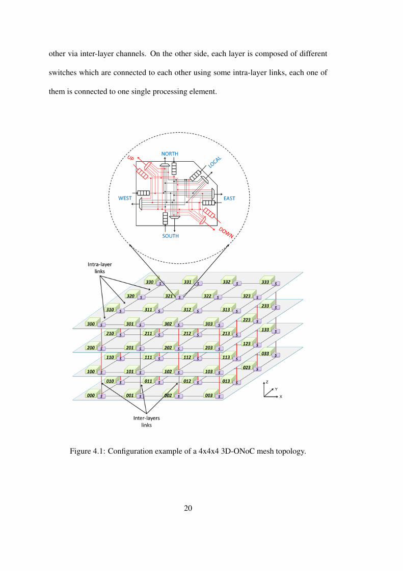
other via inter-layer channels. On the other side, each layer is composed of different
switches which are connected to each other using some intra-layer links, each one of
them is connected to one single processing element.
Figure 4.1: Configuration example of a 4x4x4 3D-ONoC mesh topology.
20

4.2 Switching policy
Considered as a very important choice for any NoC design, switching establishes
the type of connection between any upstream and downstream node. It is important
to deploy an efficient switching policy to ensure less blocking communication while
trying to minimize the system complexity. When it is related to packet switching, three
main switching policies have been mostly used for NoC: Store and Forward (SAF),
Virtual Cut Through (VCT) and Wormhole (WH) [35].
3D-ONoC adopts Wormhole-like switching and Virtual-Cut-Through forwarding
method. The forwarding method which is chosen in a given instance depends on the
level of packet fragmentation. For instance, each router in 3D-ONoC has input buffers
which can store up to four flits by default. When a packet is divided into more than four
flits, 3D-ONoC chooses Virtual-Cut-Through switching. When packets are divided
into less than four flits, the system chooses Wormhole. In other words, when buffer
size is greater than or equal to the number of flits, Virtual-Cut-Through is used, but
when buffer size is less than or equal to the number of flits, Wormhole switching is
employed. By combining the benefits of both switching techniques, packet forwarding
can be executed in an efficient way while guaranteeing a small buffer size. As a result
the system performance is enhanced while maintaining a reasonable area utilization
and power consumption.
Figure 4.2 demonstrates the 3D-ONoC 81 bits flit format. The first bit indicates the
tail bit informing the end of the packet. The next seven bits are dedicated to indicate
the Next-Port that will be used by the Look-Ahead-XYZ routing algorithm to define the
direction of the next downstream neighboring node where the flit will be sent to. Then,
21

three bits are used to store destination information of each xdest, ydest and zdest. Hav-
ing three bits for each destination field allows the network to have a maximum size of
8x8x8 3D-ONoC. But if the network size needs to be extended, the addresses fields
may also be increased to accommodate a larger network size. Finally the remaining
64 bits are dedicated to store the payload. Since 3D-ONoC is targeted for various ap-
plications, the payload size can be easily modified in order to respect the requirements
of some specific applications. Figure.4.2 shows the 3D-ONoC packet format. In addi-
tion, as we previously stated, the architecture does not provide for a separate head flit
and every flit therefore identifies its destination X, Y, and Z addresses and carries an
additional single bit to indicate whether its a tail flit or not.
Tail Next_Port X-dest Y-dest Payload
0 1 8 11 14 81
1 Bit 7 Bit 3 Bit 3 Bit 64 Bit
Z-dest
17
3 Bit
Figure 4.2: 3D-ONOC flit format.
4.3 Router architecture
The router is considered as the back-bone element in the whole 3D-ONoC design.
The 3D-ONoC router architecture is based upon the 5x5 2D-ONoC router where, as
shown in Fig.4.1, each switch has a maximum number of 7-input by 7-output port,
where 4 ports are dedicated to connect to the neighboring routers in north, east, south
and west direction using the intra-layer links. One port is used to connect the router
to the local computation tile where the packet can be injected into or ejected from
the network. The remaining two ports are added to connect the switch to the upper
22

and downer layers to ensure the inter-layer communication. As a matter of fact, the
number of ports depends on the position of the switch in the design, since we have
to eliminate any unused links that have no connections with other switches in order
to reduce power consumption. For example, as it is depicted in Fig.4.1, switch-000
have only four connected ports (north, east, up and local) and the remaining three
ports (south, west and down) have been disabled since there are no connections to any
neighboring routers along those directions.
Figure 4.3: 3D-ONoC pipeline stages: Buffer writing (BW), Routing Calculation andSwitch Allocation (RC/SA) and Crossbar Traversal stage (CT).
Figure.4.3 represents 3D-ONoC switch architecture and that the routing process at
each router can be defined by three main pipeline stages: Buffer writing (BW), Routing
Calculation and Switch Allocation (RC/SA) and finally the Crossbar Traversal stage
(CT).
3D-ONoC contains seven Input-port modules for each direction (Local, North,
23

East, South, West, Up, Down) in addition to the Switch-Allocator and Crossbar mod-
ules. Observing the Verilog HDL sample code for the Router module depicted in
Fig.4.4, we can see that each router in 3D-ONoC has five parameters showed between
line 7 and 10: NOUT which refers to the number of input-output numbers, FIFO-
DEPTH and WIDTH representing the buffer capacity and flit size respectively and
L2NET-SIZE in line 13 is the address field size in each flit. Based on these parameters
we can define the input variables by: the clock and reset signals represented by clk and
reset in line 13, the input data from all the seven input ports (data-in in line 14). The
stop signal is shown in line 15 by stop-in. xaddr, yaddr and zaddr in line 16 define
the router address in the network. Finally the output variables are the resulted pro-
cessed data and the new flow control information represented by data-out and stop-out
represented in line 18 and 19 respectively.
Figure 4.4: Verilog HDL top module of the router.
Now we analyze each component of the switch separately. Starting with the Input-
24

port, the Switch-Allocator and finally Crossbar module.
4.3.1 Input Port
Figure 4.5: Input-port module architecture.
Starting with the Input-port module (represented in Fig.4.5, each one of the seven
modules is composed of two main elements: Input buffer and the Route module.
Incoming 81 bits flits data-in from different neighboring switches, or from the con-
nected computation tile, are first stored in the Input buffer and waiting to be processed.
This step is considered as the first pipeline stage of the flit’s life-cycle (BW). Arbi-
tration between different flits is managed using FIFO queue technique. Each input
buffer has by default four as depth, which means that it can host up to four 81 bits
flits. Buffers occupy a significant portion of router area but can imply also increase in
overall performance.
After being stored, the flit is fetched form the FIFO buffer and advanced to the next
pipeline stage (RC/SA). The destination addresses (xdest, ydest and zdest) are then
25

decoded in order to extract the information about the destination address in addition
to the Next-Port pre-calculated in the previous upstream node. Those values are then
sent to the Route circuit where La-XYZ routing scheme is executed to determine the
New-next-Port direction for the next downstream node. At the same time the Next-Port
identifier is also used to generate the request for the Switch-Allocator asking for grant
to use the selected output port via sw-req and port req signals.
As we stated in Section.3, 3D-ONoC uses lookahead routing scheme LA-XYZ for
fast routing. This scheme is based upon the dimension order (DOR) X-Y-Z static
routing algorithm, where the X,Y and Z coordinates are satisfied in order. X-Y-Z
routing is presented as the vertically balanced routing algorithm which has the best
performance, since it’s simple to implement, it is free of deadlock and live-lock, and
also because packet ordering is not required. In addition to that each flit additionally
carries one hot encoded Next-Port identifier used by the downstream router. Since LA-
XYZ is based upon XYZ routing, it is considered also as a minimal routing where each
flit from any source and destination pair traverses the minimal number of hops.
To understand better how the Next-Port is decided, we designed the Verilog HDL
code depicted in Fig.4.6. As it is shown in this figure (from line 39 to 48), the routing
decision starts first by finding the next node’s address. It is done by evaluating the ac-
tual Next-Port fetched from the flit, which gives a hint about which neighboring node
the flit is going to be routed to and eventually knowing its exact address by increment-
ing xaddr or yaddr or zaddr. Depending on the resulted next address from the later
step, the new Next-Port can be determined. As demonstrated between line 50 and 69
in Fig.4.6, LA-XYZ compares the resulted next node’s address (next-xaddr, next-yaddr
26

and next-zaddr) and the destination addresses (xdest, ydest and zdest). At the end of the
execution of this comparison, the new Next-Port (defined by route in Fig.4.6) can be
determined then embedded in the flit back again to be sent to the next node as Fig.4.5
illustrates.
Figure 4.6: Verilog HDL implemntation of LA-XYZ routing algorithm.
If we take a look at Fig.4.1, and assume for example that a flit coming from switch-
200 enters switch-201 (where the xaddr, yaddr and zaddr addresses are defined by 001,
000 and 001 respectively) trying to reach its destination node switch-313 (where the
xdest, ydest and zdest addresses are defined by 011, 001 and 011 respectively). This
flit caries ”EAST” as a nextport identifier pre-calculated in the previous node (switch-
27

200). According to the he first phase of the LA-XYZ algorithm, next-xaddr= xaddr+1
which is the x-address of switch-202. In the second phase of the algorithm, next-xaddr
is then compared with xdest. The comparison result will determine ”EAST” as route
(the new Next-Port for switch-202) which will be re-updated in the flit.
In order to enable the bypass technique, two signals are issued from the buffer to
give information about the buffer occupancy status. These two signals are fifo-empty
and fifo-nearly-empty. When the fifo-empty signal is issued, it means that the input
buffer is empty and when an incoming flit arrives to the input port, it doesn’t need to
be stored in the buffer. Then overlapping the buffering stage and advancing to the next
stage (RC and SA).
4.3.2 Switch Allocator
Figure 4.7: Switch allocator circuit.
28

The sw-req and port req signals issued from each Input-port module, and giv-
ing information about the desired output-port, are transmitted to the Switch-Allocator
module to perform the arbitration between the different requests. When more than two
input flits from different input-ports are requesting the same output-port at the same
time, the Switch-Allocator manages to decide which output-port should be granted to
which input-port, and when this grant should be allocated. This process is done in
parallel with the routing computation done in Input-port to form the second pipeline
stage.
As indicated in Fig.4.7, the switch allocator circuit has two output signals: one is
sw-cntrl and the second one is grant-out. sw-cntrl contains all the information needed
by the crossbar circuit about the scheduling result as it is explained later. On the other
hand, the grant-out is sent back to the Input-port module and gives the grant to the
appropriate input-port to send its data to the crossbar before reaching its next neigh-
boring node. Figure4.7 shows that the switch allocator module is composed of two
main components: Stall-Go flow control and Matrix-Arbiter Scheduling.
Stall-Go flow control module Like the other flow control schemes, Stall-Go module
manages the case of the buffer overflow. When the buffer exceeds its limitation on
hosting flits (if the number of flits waiting for process are greater than the depth of
the buffer), a flow control has to be considered to prevent from buffer overflow and
eventually from packet dropping. Thus, allocating available resources to packets as
they progress along their route. We chose Stall-Go flow control since it proves to be
a low-overhead efficient design choice showing remarkable performance comparing
29

to the other flow control schemes such us ACK-NACK or Credit based flow control.
Like the other flow control schemes, Stall-Go module manages the case of the buffer
Figure 4.8: Stall-Go flow control mechanism.
overflow. When the buffer exceeds its limitation on hosting flits (if the number of
flits waiting for process are greater than the depth of the buffer), a flow control has to
be considered to prevent from buffer overflow and eventually from packet dropping.
Thus, allocating available resources to packets as they progress along their route. We
chose Stall-Go flow control since it proves to be a low-overhead efficient design choice
showing remarkable performance comparing to the other flow control schemes such us
ACK-NACK or Credit based flow control [36].
Stall-Go module, where the mechanism is represented in Fig.4.8, uses two control
signals: nearly-full and data-sent. nearly-full signal is sent to the upstream node in-
dicating that the input-buffer is almost full and only one slot is still available to host
one last flit. After receiving this signal, the FIFO buffers suspend sending flits. The
data-sent signal is issued when the flit is transmitted. Figure.5.10 (a) represents the
Stall-Go flow control state machine which aims to generate the nearly-full and data-
sent signals. State GO indicates that the buffer is still able to host two or more flits.
30

State SENT indicates that the buffer can host only one more flit, and finally when we
move to state STOP, it means that the buffer can not store anymore flits. The state
machine is generated as indicated in Fig.5.10 (b) that shows Verilog HDL explaining
the main state transitions using nearly-full and data-sent signals.
(a)
(b)
Figure 4.9: Stall-Go flow control: (a) State machine (b) Verilog HDL of the statemachine decision.
Matrix-Arbiter scheduling module The second component is the scheduling mod-
ule. As shown in Fig.6, the input signals sw-req and port-req indicate the input-ports
demanding the access, and which output-ports are they requesting respectively. De-
pending on these requests, the arbiter allocates the convenient output-port to its de-
31

mander. Since 3D-ONoC transmits only one flit in every clock cycle, then when two
input-ports or more are competing for the same output-port, the presence of a schedul-
ing scheme is required in order to prevent from any possible conflict. The switch
allocator in our design employs a least recently served priority scheme via the packet
transmit layer. Thus, it can treat each communication as a partially fixed transmission
latency [37], [38]. Matrix arbiter is used for a least recently served priority scheme.
In order to adopt Matrix arbiter scheduling for 3D-ONoC, we implemented a 6x6
scheduling-matrix. The scheduling module accepts all the requests from the different
connected input-ports and their requested output-ports. Then it assigns priority for each
request. In order to give the grant to the convenient input-port, the scheduling module
verifies the scheduling-matrix, compares the priorities of the input-ports competing for
the same output-port, and gives the grant to the one possessing the highest priority in
the matrix. Following this basis, the scheduling module should make the input-port,
which got the last grant to use the competed output-port, the lowest priority for the next
round of arbitration, and then increases the priority of the rest of the remaining ports.
When there are no requests, the priority is unchanged. Based on these assumptions,
we are sure that every input-port will be served and get the grant to use the output-port
in a fair way.
Figure.4.10 illustrates a simple example of how our scheduling mechanism works.
Each row of the matrix represents the competing input requests and their priorities.
The scheduling-module starts by examining the priorities of each input-port request.
After the highest priority input is served, the arbiter updates the scheduling-matrix by
making the request which got the last grant, the lowest priority for the next round of
32

arbitration, by inversing its row and column.
Figure 4.10: Scheduling-Matrix priority assignment.
The matrix shown in Fig.4.10 (a) illustrates the initial scheduling-matrix where
North, Up and Down input-ports are asking the grant to eject their flits to the Local
port. Observing this figure, the North request (highlighted in red) has higher priorities
compared with the remaining two requests. As a result the Arbiter gives the grant
to the North request. Then North becomes the lowest priority (as it is underlined by
a green line) and the remaining two requests priorities are incremented. In the next
round (Figure.4.10 (b)), Down seems to have a higher priority than the Up request.
The arbiter then gives the grant to Down and make its priority the lowest. Finally, as it
is shown in Fig.4.10 (c), the Up request having the highest priority among the others,
is giving the grant to eject its data to the requested output port.
4.3.3 Crossbar
The switch allocator, sends the issued control signal to the crossbar circuit to com-
plete the third and final Crossbar Traversal pipeline stage (CT), where information
about the selected input port and the Next-Port are embedded, and then stored in the
sw-cntrl-reg register as it is shown in Fig.4.11. After that, the crossbar fetches these
information, receives the data from the FIFO buffer of the selected input-port. Then,
33

it allocates the appropriate channel for transmission to the decoded Next-Port. Finally,
the crossbar sends the flit to its destination as illustrated in Fig.4.11. When all the flits
are transmitted, the tail bit informs the switch allocator via a tail-sent signal that the
packet transmission is completed and can free the used channel so it can be exploited
by another packet.
mux-out-L
mux-out-N
mux-out-E
mux-out-S
mux-out-W
mux-out-U
mux-out-D
data_out_L (81)
data_out_S (81)
data_out_N (81)
data_out_W (81)
data_out_E (81)
data_out_U (81)
data_out_D (81)
data_in (567)
Sw_cntrl_reg
control (49)
7/
Figure 4.11: Crossbar circuit.
4.4 Network interface
In order to enable real applications to be run on 3D-ONoC, we added a Network
Interface (NI) to every router as a medium interface between the different PEs (Pro-
cessor, memory, I/O etc...) that can be connected, and our network. In this paper, we
tested 3D-ONoC using JPEG encoder application [39]. For that reason, we designed
both Transmitter and Receiver NI in every switch of our network. We set the packet
size to 99 bits which includes three 33 bits flits. Each flit contains 17 bits defining the
34

routing information (xdst, ydst, zdst, Next-Port and tail) and the remaining 16 bits are
dedicated for the payload.
(a)
(b)
Figure 4.12: Network Interface Architecture: (a) Transmitter (b) Receiver
Figure.4.12(a) shows the architecture of the Transmitter-NI. It receives a 32 bits
data from the JPEG module that will be divided into two portions representing the
payload of the two first flits of the packet. The payload of the third flit contains the
35

10 bits control signal from the JPEG module, and the remaining six bits are unused.
As shown in Fig.4.12 (a) , a Control Module manages the fits generation. It adds the
convenient destination addresses and Next-Port direction to each flit, and marks the
end of the packet by adding the (tail bit to the third final flit. The generated flits are
then injected into the network.
On the other side, the Receiver-NI receives the incoming three flits of each packet
ejected from the network, and then stores them into three temporary registers. After
that, as it is shown in Fig.4.12 (b), the 16 bits payload of the first and second flit
are fetched form the temporary registers, reassembled together and finally stored in the
Data-reg register. Controlled by another Control Module, the complete 32 bits resulted
Data and the 10 bits control signals, are fetched the sent to their attached JPEG module
after the complete packet is received.
Based on this network interface, another one has been designed to satisfy the re-
quirements of another application that we used for evaluating 3D-ONoC, which is
Matrix-Multiplication. We chose the matrix multiplication as one of our evaluating tar-
get, since it is wildly used in scientific application. Due to its large multi-dimensional
data array, it is extremely demanding in computation power and meanwhile it is po-
tential to achieve its best performance in a parallel architecture and doesnt involve
synchronization [40]. All of these reasons make the Matrix-Multiplication a very suit-
able application to evaluate 3D-ONoC and show its outperforming performance against
2D-ONoC.
By the end of this chapter, we presented the main components of our Mesh based
36

Figure 4.13: Chip floor plan for a 2x2x2 3D-ONoC.
3D-ONoC system. We explained how the packets are forwarded among the network
using Wormhole-like switching and Virtual-Cut-Through switching policies. We also
give more details about the router components including the hardware implementation
of our proposed Look-Ahead-XYZ routing algorithm (LA-XYZ). For the flow control,
we demonstrated that 3D-ONoC adopts Stall-Go mechanism in the Switch Allocator
and how this flow control efficiently avoids dropping packets. Examples about the
Matrix-Arbiter scheduling technique are also provided to show its ability to serve all
the request in a fair way. Figure.4.13 shows the chip floor plan for a 2x2x2 3D-ONoC
for the Altera Stratix III EP3SL150F1152C2 chip, and Figure.4.14 shows the RTL
view of the same 2x2x2 3D-ONoC system. Both of these figures are generated using
the QUARTUS II tool after succeeding the correct compilation of the system.
37

Figu
re4.
14:R
TL
view
of2x
2x2
3D-O
NoC
.
38

Chapter 5
Evaluation
Using the JPEG encoder and the Matrix-multiplication applications, in this chapter
we evaluate the hardware complexity of 3D-ONoC in term of area utilization, power
consumption (static and dynamic) and clock frequency. The performance evaluation
is also done by analyzing the execution time, the number of hops and also the number
of stall after the execution of the both of the application. All the results obtained are
analyzed and compared with 2D-ONoC.
5.1 Evaluation methodology
5.1.1 JPEG encoder
Starting with the JPEG encoder application, which is a well-known application that
is widely used application by many researchers. Including some parallel processing,
JPEG might be a good application to evaluate the performance of NoC.
For instance, we took into consideration the task implementation shown in Fig.5.1.For
additional analysis, we made further divisions to the Y:d-q-h, Cb:d-q-h, Cr:d-q-h and
FIFO modules, and the resulted task graph is illustrated in Fig.5.2. This extension aims
to increase the network size and deploy more parallel execution of the different mod-
ules of the application, and then can take advantage of the scalability and the reduced
39

Figure 5.1: Task graph of the JPEG encoder
number of hops offered by our design.
As we analyze the modified task graph represented in Fig.5.2, we noticed that
the communication bandwidth between DCT, Quantization and Huffman modules are
very high (640 bits) compared with those found between the different other modules
of the application (8, 24 and 32 bits). This bandwidth gap will cause unbalanced traffic
distribution especially when implemented on hardware, since we will increase the link
size in addition to the size and number of flits in the packet format, causing higher
latency and thermal power problem. All these factors, will eventually decrease the
overall performance of our system, instead of enhancing it.
For all the reasons previously stated, we will implement the first task graph rep-
resented in Fig.5.1 and we randomly mapped the tasks into 2D-ONoC (2x4) and 3D-
ONoC (2x2x2) as shown in Fig.5.3 (a) and Fig.5.3 (b) respectively.
40

Figure 5.2: Extended task graph of the JPEG encoder
41

(a) (b)
Figure 5.3: JPEG encoder mapped onto: (a) 2x4 2D-ONoC (b) 2x2x2 3D-ONoC
5.1.2 Matrix multiplication
Figure 5.4: Matrix multiplication example: The multiplication of an ixk matrix A by akxj matrix B results in an ixj matrix R.
First we assume that an ixk matrix A has i rows and k columns, where Aik is an
element of A at the i-th row and k-th column. As it demonstrated in Fig.5.4, an ixk ma-
trix A can be multiplied by a kxj matrix B to obtain an ixj matrix R. Figure.5.5 presents
how the matrix R can be obtained according to Formula 4.1.
Ri,j =k−1∑n=0
Ai,n.Bn,k (5.1)
When implemented onto 3D-ONoC, and for seek of convenience or without loss
in generality, we can assume that all the matrices are square and having nxn size. In
3D-ONoC, each element of the three matrices is assigned to a computation module
which is connected to one router. As a result the number of routers connected to the
42

Figure 5.5: Simple example demonstrating the Matrix multiplication calculation.
network is the sum of all the elements of three matrices which is equal to 3n2. Each
element of the matrix B receives n flits from n different elements of the matrix A in
order to make the multiplication. Then, each element of the matrix B sends n flits to n
different elements of the matrix R where all the received values are summed then the
final resulted value is outputted. In total 2n3 flits travel the network for a nxn square
matrix multiplication.
As we previously stated at the beginning of this chapter, we want to evaluate the
number of hops traversed by all the flits generated by the Matrix application. For this
matter we define:
3D Hopsi = |x desti − x srci|+ |y desti − y srci|+ |z desti − z srci| (5.2)
Where 3D Hopsi is the number of hops consumed for one single flit i ∈ {0,1,2,....,2n3-
1} (the set of all flits), traveling from one source node (where the address is defined by
x dest, y dest and z dest) to its destination node (x src, y src and z src). As a result,
we can say that the number of hops consumed by an nxn square matrix multiplication
43

can be defined by:
3D Total Hops =2n3−1∑k=0
3D Hopsk (5.3)
According to Formula 4.2 and 4.3, the number of hops for 2D-ONoC can be then ex-
tracted and defined as follow:
2D Hopsi = |x desti − x srci|+ |y desti − y srci| (5.4)
2D Total Hops =2n3−1∑k=0
2D Hopsk (5.5)
For the evaluation, we took the case of 3x3, 4x4 and finally a 6x6 matrix multiplication.
For each one of these three cases, two mapping approaches has been taken into consid-
eration. For instance, we take the example of 3x3 matrix multiplication. We randomly
mapped the elements of the three matrices into 2D-ONoC (3x9) and 3D-ONoC (3x3x3)
using an optimistic mapping approach as presented in Fig.5.6 (a). In this mapping we
tried to make the communication distance as close as possible, in order to reduce the
number of hops which eventually will lead to decrease the latency. Figure.5.6 (b), on
the other hand, illustrates a pessimistic task mapping approach. The second approach
tries to increase the communication path of the different flits traversing the network.
44

(a)
(b)
Figu
re5.
6:3x
3m
atri
xm
ultip
licat
ion
usin
g(a
)opt
imis
tican
d(b
)pes
sim
istic
map
ping
appr
oach
es
45

In order to obtain an easier and more accurate evaluation both of 3D-ONC is im-
plemented in Verilog HDL. We evaluated and compared the hardware complexity in
terms of area, power consumption (static and dynamic) and clock frequency and also
the performance in term execution time, the number of hops, and also we counted the
number of stop-signal generated from our Stall-Go flow control mechanism. All the
evaluation results obtained for 3D-ONoC are than compared to 2D-ONoC system.
We chose the Stratix III FPGA as a target device and then the synthesis was done
by the Quartus II software, which both are provided by Altera inc.. We used PowerPlay
Power Analyzer tool in QuartusII in order to evaluate the power consumption gener-
ated. This design approach results in more accurate speed, area and power consump-
tion evaluation. The use of FPGA is a very convenient choice for our design, thanks to
its simplicity and the ability of reconfigurability. In addition to that, it provides faster
simulation than the traditional software emulation while maintaining a cheaper cost
than implementing with real processors. Table.5.1 presents the parameters used for the
synthesis of 3D-ONoC design
5.2 Evaluation results
5.2.1 Hardware complexity evaluation
As we previously stated, the goal of this section is to provide a hardware evalua-
tion for our 3D-ONoC including area, power consumption, and clock frequency when
simulated with both JPEG encoder and Matrix multiplication applications.
Table.5.2 illustrates the hardware evaluation results obtained. The results show that
the logic utilization of 3D-ONoC is increased by an average of 37% compared to the
2D design. The increased number of ALUTs can be explained by the fact that the
46

Table 5.1: Simulation parameters.
Parameters 2D-ONoC 3D-ONoC
Network SizeJPEG 2x4 2x2x2
(Mesh)Matrix (3x3) 3x9 3x3x3Matrix (4x4) 6x8 4x4x3Matrix (6x6) 9x12 6x6x3
Packet sizeJPEG 3 flits 3 flitsMatrix 1 flit 1 flit
Flit sizeJPEG 30 bits 33 bitsMatrix 35 bits 30 bits
Header sizeJPEG 12 bits 17 bitsMatrix 14 bits 17 bits
Payload sizeJPEG 16 bits 16 bitsMatrix 21 bits 21 bits
Buffer Depth 4 4Switching Wormhole-like Wormhole-like
Flow control Stall-Go Stall-GoScheduling Matrix-Arbiter Matrix-Arbiter
Routing LA-XY LA-XYZTarget Device Altera Stratix III Altera Stratix III
3D-ONoC router has two additional ports and a larger crossbar than 2D-ONoC. The
additional number of ports incurs additional buffers, which is costly in term of area.
In term of clock speed 3D ONoC under-performs the 2D-ONoC architecture by
16% on average due to the increased hardware complexity. While the power static
consumption is increased with 3D-ONoC with almost 14% for the same additional
hardware reasons, the dynamic power on the other hands is decreased in average of
16% while executing JPEG and the two mapping approaches foe each of the three
matrix multiplications. As a conclusion, the total power consumption is decreased
with nearly 1.4%.
Many factors affect the dynamic power in FPGA, such us capacitance charging,
supply voltage and clock frequency. Since the first two factors are the same for both
47

Table 5.2: 3D-ONoC hardware complexity compared with 2D-ONoC.Application Area (ALUTs) Power(mW) Speed(MHz)
2D 3D 2D 3D 2D 3DStatic Dynamic Total Static Dynamic Total
JPEG 28.401 30.382 811.63 4.27 815.9 769.13 4.01 773.14 193.8 160.72Matrix 3x3 18.012 30.954 969.84 332 1301.84 1032.14 260 1292.14 158.73 130.01Matrix 4x4 36.393 61.157 1073.52 495.2 1568.72 1055.65 410 1452.65 146.56 101.41Matrix 6x6 89.576 144.987 1113.29 580 1693.29 1051.06 450.2 1501.26 98.85 98.1
3D and 2D ONoC designs, and only the clock frequency is different between them,
we can say that the reduction of the clock frequency had an impact on the reduction
of the dynamic power. Besides that the clock frequency reduction, we believe that the
reduction of number of hops (that will be explained in the next section) also plays an
important role in the reduction of dynamic power. In fact, when the number of hops is
reduced it means that the flit has less hops, shorter path which eventually means less
buffering, routing and scheduling. All these factors lead to reduce the dynamic power
when using 3D-ONoC when compared with 2D system.
5.2.2 Performance analysis evaluation
For the performance evaluation, we run each of the four applications. Then we
evaluated the execution time, the number of hops and the number of stop-signal of
each one of them after verifying the correctness of the resulted data.
Starting with the execution time, we run each of the four applications on 3D-ONoC
and 2D-ONoC. Figure.5.7 demonstrates the execution time results. Taking a closer
look at the JPEG application results, we may see that there is a slight improvement of
1.4% with 3D-ONoC when compared with the 2D architecture. This slight improve-
ment can be explained by many reasons.
First, JPEG is a small application which we could map into only eight nodes. That
48

is a quiet small number to exploit the benefits of a 3D-NoC. Seconds, when observing
the task graph of JPEG (previously shown in Fig.5.1), JPEG has indeed some tasks
working in parallel(Y:d-q-h, Cb:d-q-h and Cr:d-q-h), but at the same time we can see
that FIFO module is dependent of those three tasks. Another reason is, the JPEG
computation modules involve heavy computation. This leads to decrease the clock
frequency of the entire system in a very inconvenient way for 3D-ONoC. The perfor-
mance of 3D-ONoC is then hided and can’t be taken advantage of. All of those reasons
have an important impact on the performance of the 3D-ONoC. JPEG might be a very
appropriate application to show the out performance of NoC over the traditional inter-
connect systems (such us bus-based system or P2P), but when we talk about 3D-ONoC
that is targeted for hundreds of cores which is dedicated to a large number of cores with
higher parallelism tasks.
Figure 5.7: Execution time comparison between 3D and 2D ONoC.
On the other part, when evaluated with the Matrix multiplication application, 3D-
ONoC shows a greater performance and decreases the execution time for about 35%,
49

33% and 41% for each of 3x3, 4x4 and 6x6 matrix respectively. In total 3D-ONoC
reduces the execution time for one single Matrix multiplication to up to 36% when
compared with 2D-ONoC. As we stated previously, due to the fact that the Matrix
multiplication has a larger data array, higher number of parallel tasks with less de-
pendency between them, Matrix multiplication shows greater performance than JPEG.
While the JPEG is mapped onto 8 nodes only, the matrix multiplication can reach the
108 nodes for the 6x6 matrix size. These factors are very suitable to show the per-
formance enhancement when adopting 3D-ONoC. This enhancement can be related to
the reduction of number of hops that offers 3D-ONoC. Figure.5.8 show the variation
of the number of hops between 3D-ONoc and 2D-ONoC with 3x3, 4x4 and 6x6 matrix
multiplication using pessimistic and optimistic mapping.
50

(a)
(b)
(c)
Figu
re5.
8:A
vera
genu
mbe
rofh
ops
com
pari
son
forb
oth
pess
imis
tican
dop
timis
ticm
appi
ng:(
a)3x
3(b
)4x4
(c)6
x6.
51

When we analyze this figure, we may see that 3D-ONoC reduces the number of
hops compared with the 2D system with an average percentage of 42%, 31% and 47%
3x3, 4x4 and 6x6 matrices respectively having a total number of hops reduction of
40% over the 2D architecture. This can significantly reduce the execution time, since
flits have fewer hops to traverse to reach their destination. Another reason contributing
on the performance of 3D-ONoC is the reduction of the traffic congestion. This can be
seen by observing the Stall-Go flow control and the number of stop-signal generated
by each Matrix Multiplication. As a matter of fact when observing Fig.5.9, we can
Figure 5.9: Stall average count comparison between 3D and 2D ONoC.
see that the stall count increase linearly when we increase the matrix which is related
to the number of flits traveling the network. Even 3D-ONoC can reach up to 77% of
stall count reduction over the 2D design with 6x6 Matrix multiplication, the stall count
impact cannot be clearly seen with 3x3 and 4x4 calculation. This can simply explained
by the fact that we are calculating a single matrix multiplication which generates only
52

54 and 128 flits for 3x3 and 4x4 matrix size respectively. This small number of flits
was not enough to cause any trafiic congestions in 3D-ONoC. For that reason, we
decide to extend the evaluation to calculate not only one Matrix multiplication but also
to calculate 2, 3 and 4 different matrices at the same. This aims to increase the number
of flits traveling the network at the same time to cause congestion. Then we evaluate
again the average stall count.
Figure.5.10, depicts the average stall count of both 3D and 2D ONoC when imple-
mented with 1, 2, 3 and 4 matrix multiplications. When analyzing this figure, the stall
count has been dramatically decreased to 94%, 67% and 59% in average for 3x3, 4x4
and 6x6 matrix Multiplication respectively. In total 3D-ONoC reduces the stall count
to up to 74%.
Figure 5.10: Stall average count comparison between 3D and 2D ONoC with differenttraffic loads.
After calculating the stall number, we want to see the impact of increasing the
53

traffic congestion on the execution time. So evaluate again the execution time of each
Matrix size when performing 1, 2, 3 and 4 matrix multiplications. The result obtained
are shown in Fig.5.11 reduces the execution time to 36%, 39% and 47% for 3x3, 4x4
and 6x6 matrix Multiplication respectively. Then improving the total execution time
reduction from 36%, obtained in the first experience with one matrix multiplication, to
more than 41% when evaluated with heavier traffic load.
Figure 5.11: Execution time comparison between 3D and 2D ONoC with differenttraffic loads.
As the results mentioned above, 3D-ONoC take advantage of its ability to reduce
the number of hops to enhance the performance. In addition, since 3D-ONoC router
has two additional input-output ports, flits traveling the network have better routing
choices which eventually will decrease the congestion that can be caused when using
2D-ONoC, having an important impact on the overall performance of the system. Not
forget to mention, this will improve the traffic balance along the whole network which
54

plays a very crucial role on the thermal power dissipated from the design.
55

Chapter 6
Conclusion and Future Work
3D-ONoC is a natural extension of the 2D-ONoC design previously developed by
our group. In this paper we present a hardware design for 3D-OASIS Network-on-Chip
(3D-ONoC) including complete details about the main components of the design. We
also present a preliminary hardware and performance evaluation results using JPEG
encoder Matrix multiplication applications.
Evaluation results show that in term of speed 3D-ONoC under-performs 2D-ONoC
architecture with 16% observing a 37% area utilization penalty and a slight improve-
ment of 1.4% in total power consumption. Despite the increasing hardware complexity,
3D ONoC shows an improvement in term of execution time by reducing the delay to
28% in overall compared to the 2D architecture. We explained that by the fact that 3D-
ONoC decreases the number of hops by 40% and also the average stall count to 74%.
In a second experience we proved that by increasing the traffic load with the Matrix
application, we can enhance the execution time reduction from 36% obtained with one
matrix multiplication to more than 41% with 1, 2, 3 and 4 matrix multiplications.
As a future work, we will try to optimize the routing algorithm in order to enhance
56

the performance of our design. We will try also to optimize the router architecture,
especially the input buffers which is one of the most important reason of the area
penalty. This aims to obtain an enhanced design of 3D-ONoC that increase the per-
formance while keeping the hardware cost balanced and reasonable. Also, a thermal
power study should be done to observe how 3D-ONoC deals with such important per-
formance requirement.
57

References
[1] A. Habibi,M. Arjomand, H. Sarbazi-Azad , Multicast-Aware Mapping Algo-
rithm for On-chip Networks, 19th International Euromicro Conference on Par-
allel, Distributed and Network-Based Processing, Feb 2011 pp. 455-462 .
[2] G. Leary, Karam S. Chatha, Design of NoC for SoC with Multiple Use Cases
Requiring Guaranteed Performance, 23rd International Conference on VLSI
Design, January 2010 pp. 200-205 .
[3] R. Kumar, V. Zyuban, and D. M. Tullsen. Interconnections in Multicore Ar-
chitectures: Understanding Mechanisms, Overheads and Scaling. Proc. of the
32nd Int. Sym. on Comp. Arch., pp. 408-419, Madison, USA, 2005.
[4] A. Ben Abdallah, M. Sowa, Basic, Network-on-Chip Interconnection for Fu-
ture Gigascale MCSoCs Applications: Communication and Computation Or-
thogonalization, Proc. of The TJASSST2006 Symposium on Science, DEC.
2006.
[5] J. Kim, D. Park, T. Theocharides, V. Narayanan, C. Das. A Low Latency
Router Supporting Adaptivity for On-Chip Interconnects. Proc. of the 42nd
Conf. on Design Auto., pp. 559-564, 2005.
58

[6] J. Kim, C. Nicopoulos, D. Park, V. Narayanan, M. S. Yousif, and C. R. Das. A
Gracefully Degrading and Energy-Efficient Modular Router Architecture for
On-Chip Networks. Proc. of the 33rd Int. Sym. on Comp. Arch., pp. 138-149,
2006.
[7] A. Kumar, L.-S. Peh, P. Kundu, and N. K. Jha. Express Virtual Channels: To-
wards the Ideal Interconnection Fabric. Proc. of the 34th Int. Sym. on Comp.
Arch., pp. 150-161, 2007.
[8] R. Mullins, A. West, and S. Moore. Low-Latency Virtual-Channel Routers for
On-Chip Networks. Proc. of the 31st Int. Sym. on Comp. Arch., pp. 188-197,
2004.
[9] W. J. Dally. Express Cubes: Improving the Performance of kary-n-cube Inter-
connection Networks. IEEE Trans. on Computers, 40(9):1016-1023, 1991.
[10] J. Kim, J. Balfour, and W. J. Dally. Flatterned Butterfly Topology for On-Chip
Networks. Proc. of the 40th Int. Sym. on Microarchitecture, pp. 172-182, 2007.
[11] U. Y. O. and R. Marculescu. Its a Small World After All: NoC Performance
Optimization via Long-Range Link Insertion. IEEE Trans. on VLSI Sys.,
14(7):693-706, July 2006.
[12] G. Philip, B. Christopher, and P. Ramm, Handbook of 3D Integration: Tech-
nology and Applications of 3D Integrated Circuits, Wiley-VCH, 2008.
59

[13] S. Das et al. Technology, Performance, and Computer Aided Design of Three-
Dimensional Integrated Circuits. In Proc. International Symposium on Physi-
cal Design, 2004.
[14] P. Morrow, M. Kobrinsky, S. Ramanathan, C.-M. Park, M. Harmes, V. Ra-
machandrarao, H. Park, G. Kloster, S. List, and S. Kim. Wafer-Level 3D Inter-
connects Via Cu Bonding. In Proc. the 21st Advanced Metallization Confer-
ence, Oct. 2004.
[15] J. Joyner, P. Zarkesh-Ha, and J. Meindl. A stochastic global net-length distri-
bution for a three-dimensional system-on-chip(3D-SoC). In Proc. 14th Annual
IEEE International ASIC/SOC Conference, Sept. 2001.
[16] A. W. Topol, J. D. C. La Tulipe, L. Shi, D. J. Frank, K. Bernstein, S. E. Steen,
A. Kumar, G. U. Singco, A. M. Young, K. W. Guarini, and M. Ieong, Three-
dimensional integrated circuits, IBM Journal of Research and Development,
vol. 50, no. 4/5, pp. 491506, July 2006.
[17] L. P. Carloni, P. Pande, and Y. Xie, Networks-on-chip in emerging interconnect
paradigms: Advantages and challenges, In Proceedings of the 3rd ACM/IEEE
International Symposium on Networks-on-Chip (NOCS09), San Diego, CA,
May 2009, pp. 93-102.
[18] F. Li, C. Nicopoulos, T. D. Richardson, Y. Xie, N. Vijaykrishnan, M. T. Kan-
demir: Design and Management of 3D Chip Multiprocessors Using Network-
in-Memory. ISCA 2006: 130-141
60

[19] K. Mori, A. Ben Abdallah, K. Kuroda, Design and Evaluation of a Complexity
Effective Network-on-Chip Architecture on FPGA, Proc. of The 19th Intelli-
gent System Symposium (FAN 2009), pp.318-321, Sep. 2009.
[20] K. Mori, A. Esch, A. Ben Abdallah, K. Kuroda, Advanced Design Issues for
OASIS Network-on-Chip Architecture, IEEE Proc. of the 5th International
Conference on Broadband, Wireless Computing, Communication and Appli-
cations (BWCCA-2010), Nov. 2010, pp. 74-79.
[21] B. Feero, P. Pratim Pande, Performance Evaluation for Three-Dimensional
Networks-on-Chip, Proceedings of IEEE Computer Society Annual Sympo-
sium on VLSI (ISVLSI), 9th-11th May 2007, pp. 305-310.
[22] V. F. Pavlidis, E.G. Friedman, 3-D Topologies for Networks-on-chip, IEEE
Transactions on VLSI Systems, Oct. 2007, pp. 1081-1090.
[23] F. Li, C. Nicopoulos, T. Richardson, Y. Xie, V. Narayanan, and M. Kan-
demir. Design and management of 3D chip multiprocessors using network-
in-memory. ACM SIGARCH Computer Architecture News, 34(2):130?141,
2006.
[24] S. Yan and B. Lin. Design of application-specific 3D networks-on-chip ar-
chitectures. In Proceedings of International Conference of Computer Design,
pages 142149, Oct. 2008.
[25] C. J. Glass and L. M. Ni, ”The Turn Model for Adaptive Routing”, in Proc.19th
Ann. Int’l Symp. Computer Architecture, May 1992, pp. 278-287.
61

[26] J. Hu and R. Marculescu, Exploiting the Routing Flexibility for En-
ergy/Performance Aware Mapping of Regular NoC Architectures, in Proc.
DATE’03, 2003, pp. 688-693.
[27] R. S. Ramanujam and B. Lin, Near-optimal oblivious routing on threedimen-
sional mesh networks, in Proc. IEEE Int. Conf. Comp. Design, Lake Tahoe,
CA, 2008.
[28] C. H. Chao, K. Y. Jheng, H. Y. Wang, J. C. Wu, and An-Yeu Wu, ”Traffic- and
thermal-aware run-time thermal management scheme for 3D NoC systems,”
in Proc. ACM/IEEE Int. Symp. Networks-on-Chip (NoCS), Grenoble, France,
May 2010, pp. 223-230.
[29] S. TYAGI, EXTENDED BALANCED DIMENSION ORDERED ROUTING
ALGORITHM FOR 3D-NETWORKS, Centre for Development of Advance
Computing, Noida, (U.P.), India International Conference on Parallel rocessing
Workshops, pp 499-506, 2009 http://www.iacqer.com/Proceedings
[30] J. M. Montaana, M. Koibuchi, H. Matsutani, H. Amano, Balanced Dimension-
Order Routing for k-ary n-cubes, Department of Information and Computer
Science,Keio University, Yokohama, Japan, International Conference on Par-
allel rocessing Workshops, pp 499-506, 2009
[31] K. Lahiri, A. Raghunathan, and S. Dey, Efficient Exploration of the SoC Com-
munication Architecture Design Space, in Proc. IEEE/ACM ICCAD’00, 2000,
, pp. 424-430.
62

[32] K. Dev, Multi-Objective Optimization using evolutionary Algorithms, John
Wiley and Sons Ltd, 2002, pp. 245-253.
[33] L. Xin and C.-s. Choy, A Low-latency NoC Router with Lookahead Bypass, in
IEEE Int. Symp. pn Circuits and Systems (ISCAS), 2010, pp.39813984.
[34] A Ben Ahmed, A. Ben Abdallah, K. Kuroda, Architecture and Design of Effi-
cient 3D Network-on-Chip (3D NoC) for Custom Multicore SoC, IEEE Proc.
of BWCCA-2010, Nov. 2010.
[35] M. S. Rasmussen, ”Network-on-Chip in Digital Hearing Aids”, Informat-
ics and Mathematical Modelling, Technical University of Denmark, DTU,
Richard Petersens Plads, Building 321, DK-2800 Kgs. Lyngby, IMM-Thesis-
2006-76, 2006.
[36] A. Pullini , F. Angiolini , D. Bertozzi and L. Benini, Fault tolerance over-
head in network-on-chip flow control schemes, Proceedings of the 18th annual
symposium on Integrated circuits and system design, Florianolpolis, Brazil,
September 04-07, 2005, pp.224 - 229
[37] B. T. Gold. ”Balancing Performance, Area, and Power in an On-Chip Net-
work.”, Master’s thesis, Department of Electrical and Computer Engineering,
Virginia Tech, August 2004.
[38] Z, Fu and X. Ling ”The design and implementation of arbiters for Network-on-
chips.” IEEE, Industrial and Information Systems (IIS), 2010 2nd International
Conference, vol. 1, p. 292-295, 2010
63

[39] J. Rosethal, JPEG Image Compression Using an FPGA, Master of Science in
Electrical and Computer Engineering, University of California Santa Barbara
DEC. 2006.
[40] Z. WANG and O. HAMMAMI. ”A 24 Processors System on Chip FPGA De-
sign with Network on Chip”.
64