On Semiconductor - MC7805CT - Positive Voltage Regulator
29
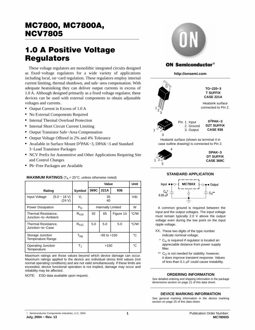
Semiconductor Components Industries, LLC, 2004 July, 2004 - Rev. 13 1 Publication Order Number: MC7800/D MC7800, MC7800A, NCV7805 1.0 A Positive Voltage Regulators These voltage regulators are monolithic integrated circuits designed as fixed-voltage regulators for a wide variety of applications including local, on-card regulation. These regulators employ internal current limiting, thermal shutdown, and safe-area compensation. With adequate heatsinking they can deliver output currents in excess of 1.0 A. Although designed primarily as a fixed voltage regulator, these devices can be used with external components to obtain adjustable voltages and currents. • Output Current in Excess of 1.0 A • No External Components Required • Internal Thermal Overload Protection • Internal Short Circuit Current Limiting • Output Transistor Safe-Area Compensation • Output Voltage Offered in 2% and 4% Tolerance • Available in Surface Mount D 2 PAK-3, DPAK-3 and Standard 3-Lead Transistor Packages • NCV Prefix for Automotive and Other Applications Requiring Site and Control Changes • Pb-Free Packages are Available MAXIMUM RATINGS (T A = 25°C, unless otherwise noted) Value Unit Rating Symbol 369C 221A 936 Input Voltage (5.0 - 18 V) (24 V) V I 35 40 Vdc Power Dissipation P D Internally Limited W Thermal Resistance, Junction-to-Ambient R qJA 92 65 Figure 14 °C/W Thermal Resistance, Junction-to-Case R qJC 5.0 5.0 5.0 °C/W Storage Junction Temperature Range T stg -65 to +150 °C Operating Junction Temperature T J +150 °C Maximum ratings are those values beyond which device damage can occur. Maximum ratings applied to the device are individual stress limit values (not normal operating conditions) and are not valid simultaneously. If these limits are exceeded, device functional operation is not implied, damage may occur and reliability may be affected. NOTE: ESD data available upon request. TO-220-3 T SUFFIX CASE 221A 1 D 2 PAK-3 D2T SUFFIX CASE 936 2 3 See detailed ordering and shipping information in the package dimensions section on page 21 of this data sheet. ORDERING INFORMATION Heatsink surface connected to Pin 2. Pin 1. Input 2. Ground 3. Output Heatsink surface (shown as terminal 4 in case outline drawing) is connected to Pin 2. 1 3 STANDARD APPLICATION A common ground is required between the input and the output voltages. The input voltage must remain typically 2.0 V above the output voltage even during the low point on the input ripple voltage. XX, MC78XX Input C in * 0.33 mF C O ** Output These two digits of the type number indicate nominal voltage. C in is required if regulator is located an appreciable distance from power supply filter. C O is not needed for stability; however, it does improve transient response. Values of less than 0.1 mF could cause instability. * ** See general marking information in the device marking section on page 25 of this data sheet. DEVICE MARKING INFORMATION DPAK-3 DT SUFFIX CASE 369C http://onsemi.com 1 2 3 4
-
Upload
abel-hernandez -
Category
Documents
-
view
21 -
download
1
Transcript of On Semiconductor - MC7805CT - Positive Voltage Regulator
Semiconductor Components Industries, LLC, 2004
July, 2004 − Rev. 131 Publication Order Number:
MC7800/D
MC7800, MC7800A,NCV7805
1.0 A Positive VoltageRegulators
These voltage regulators are monolithic integrated circuits designedas fixed−voltage regulators for a wide variety of applicationsincluding local, on−card regulation. These regulators employ internalcurrent limiting, thermal shutdown, and safe−area compensation. Withadequate heatsinking they can deliver output currents in excess of1.0 A. Although designed primarily as a fixed voltage regulator, thesedevices can be used with external components to obtain adjustablevoltages and currents.• Output Current in Excess of 1.0 A
• No External Components Required
• Internal Thermal Overload Protection
• Internal Short Circuit Current Limiting
• Output Transistor Safe−Area Compensation
• Output Voltage Offered in 2% and 4% Tolerance
• Available in Surface Mount D2PAK−3, DPAK−3 and Standard3−Lead Transistor Packages
• NCV Prefix for Automotive and Other Applications Requiring Siteand Control Changes
• Pb−Free Packages are Available
MAXIMUM RATINGS (TA = 25°C, unless otherwise noted)
Value Unit
Rating Symbol 369C 221A 936
Input Voltage (5.0 − 18 V)(24 V)
VI 3540
Vdc
Power Dissipation PD Internally Limited W
Thermal Resistance,Junction−to−Ambient
RJA 92 65 Figure 14 °C/W
Thermal Resistance,Junction−to−Case
RJC 5.0 5.0 5.0 °C/W
Storage JunctionTemperature Range
Tstg −65 to +150 °C
Operating JunctionTemperature
TJ +150 °C
Maximum ratings are those values beyond which device damage can occur.Maximum ratings applied to the device are individual stress limit values (notnormal operating conditions) and are not valid simultaneously. If these limits areexceeded, device functional operation is not implied, damage may occur andreliability may be affected.
NOTE: ESD data available upon request.
TO−220−3T SUFFIX
CASE 221A
1
D2PAK−3D2T SUFFIXCASE 936
2
3
See detailed ordering and shipping information in the packagedimensions section on page 21 of this data sheet.
ORDERING INFORMATION
Heatsink surfaceconnected to Pin 2.
Pin 1. Input2. Ground3. Output
Heatsink surface (shown as terminal 4 incase outline drawing) is connected to Pin 2.
1
3
STANDARD APPLICATION
A common ground is required between theinput and the output voltages. The input voltagemust remain typically 2.0 V above the outputvoltage even during the low point on the inputripple voltage.
XX,
MC78XXInput
Cin*0.33 F
CO**
Output
These two digits of the type number indicate nominal voltage.
Cin is required if regulator is located anappreciable distance from power supplyfilter.
CO is not needed for stability; however,it does improve transient response. Values of less than 0.1 F could cause instability.
*
**
See general marking information in the device markingsection on page 25 of this data sheet.
DEVICE MARKING INFORMATION
DPAK−3DT SUFFIXCASE 369C
http://onsemi.com
1 23
4
MC7800, MC7800A, NCV7805
http://onsemi.com2
R15680R18
100 k
D1Zener
R110.66 k
R21.56 k
R179.0 k
Q7QNPN
LATQ17
Q9QNPN 2
Q8QNPN
Q14QNPN
Q6QNPN
Q5QNPN 2
LAT 3 AQ18
R54.5 k
R61.0 k
Q13QNPN
Q2QNPN 4
SUBQ11 2
R1115 k
QNPN 6
Q1
R714 k
R31.8 k
R85.0 k
Diode
Q16
Q4QNPN
N+
C130 PC2
3.0 P
R93.0 k
R16600
R2017500
Q15QNPN
Q10QNPN
R22100
Q12QNPN
R2450
1.0 P
R21600
R230.2
R1927.5 k
D2Zener
Q19QNPN
R141.0 k
Q20QNPN
R289.0 k
R279.0 k
R299.0 k
R256.0 k
R263.0 k
R123.0 k
R103340−(3316ACT)
R3018 k
Sense
Vout5.01
Vin
R1311660
Q3QNPN
MC7800
C3
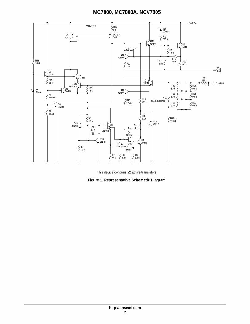
Figure 1. Representative Schematic Diagram
This device contains 22 active transistors.
MC7800, MC7800A, NCV7805
http://onsemi.com3
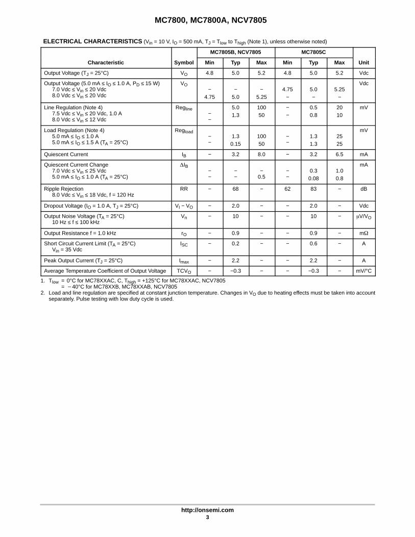
ELECTRICAL CHARACTERISTICS (Vin = 10 V, IO = 500 mA, TJ = Tlow to Thigh (Note 1), unless otherwise noted)
MC7805B, NCV7805 MC7805C
Characteristic Symbol Min Typ Max Min Typ Max Unit
Output Voltage (TJ = 25°C) VO 4.8 5.0 5.2 4.8 5.0 5.2 Vdc
Output Voltage (5.0 mA ≤ IO ≤ 1.0 A, PD ≤ 15 W)7.0 Vdc ≤ Vin ≤ 20 Vdc8.0 Vdc ≤ Vin ≤ 20 Vdc
VO−
4.75−
5.0−
5.254.75
−5.0−
5.25−
Vdc
Line Regulation (Note 4)7.5 Vdc ≤ Vin ≤ 20 Vdc, 1.0 A8.0 Vdc ≤ Vin ≤ 12 Vdc
Regline−−
5.01.3
10050
−−
0.50.8
2010
mV
Load Regulation (Note 4)5.0 mA ≤ IO ≤ 1.0 A5.0 mA ≤ IO ≤ 1.5 A (TA = 25°C)
Regload−−
1.30.15
10050
−−
1.31.3
2525
mV
Quiescent Current IB − 3.2 8.0 − 3.2 6.5 mA
Quiescent Current Change7.0 Vdc ≤ Vin ≤ 25 Vdc5.0 mA ≤ IO ≤ 1.0 A (TA = 25°C)
IB−−
−−
−0.5
−−
0.30.08
1.00.8
mA
Ripple Rejection8.0 Vdc ≤ Vin ≤ 18 Vdc, f = 120 Hz
RR − 68 − 62 83 − dB
Dropout Voltage (IO = 1.0 A, TJ = 25°C) VI − VO − 2.0 − − 2.0 − Vdc
Output Noise Voltage (TA = 25°C)10 Hz ≤ f ≤ 100 kHz
Vn − 10 − − 10 − V/VO
Output Resistance f = 1.0 kHz rO − 0.9 − − 0.9 − m
Short Circuit Current Limit (TA = 25°C)Vin = 35 Vdc
ISC − 0.2 − − 0.6 − A
Peak Output Current (TJ = 25°C) Imax − 2.2 − − 2.2 − A
Average Temperature Coefficient of Output Voltage TCVO − −0.3 − − −0.3 − mV/°C
1. Tlow = 0°C for MC78XXAC, C, Thigh = +125°C for MC78XXAC, NCV7805= 40°C for MC78XXB, MC78XXAB, NCV7805
2. Load and line regulation are specified at constant junction temperature. Changes in VO due to heating effects must be taken into accountseparately. Pulse testing with low duty cycle is used.
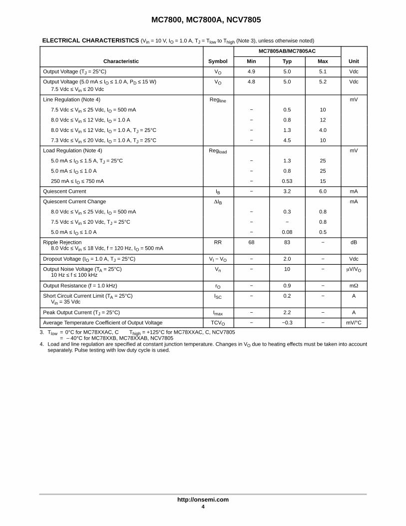
MC7800, MC7800A, NCV7805
http://onsemi.com4
ELECTRICAL CHARACTERISTICS (Vin = 10 V, IO = 1.0 A, TJ = Tlow to Thigh (Note 3), unless otherwise noted)
MC7805AB/MC7805AC
Characteristic Symbol Min Typ Max Unit
Output Voltage (TJ = 25°C) VO 4.9 5.0 5.1 Vdc
Output Voltage (5.0 mA ≤ IO ≤ 1.0 A, PD ≤ 15 W)7.5 Vdc ≤ Vin ≤ 20 Vdc
VO 4.8 5.0 5.2 Vdc
Line Regulation (Note 4) Regline mV
7.5 Vdc ≤ Vin ≤ 25 Vdc, IO = 500 mA − 0.5 10
8.0 Vdc ≤ Vin ≤ 12 Vdc, IO = 1.0 A − 0.8 12
8.0 Vdc ≤ Vin ≤ 12 Vdc, IO = 1.0 A, TJ = 25°C − 1.3 4.0
7.3 Vdc ≤ Vin ≤ 20 Vdc, IO = 1.0 A, TJ = 25°C − 4.5 10
Load Regulation (Note 4) Regload mV
5.0 mA ≤ IO ≤ 1.5 A, TJ = 25°C − 1.3 25
5.0 mA ≤ IO ≤ 1.0 A − 0.8 25
250 mA ≤ IO ≤ 750 mA − 0.53 15
Quiescent Current IB − 3.2 6.0 mA
Quiescent Current Change IB mA
8.0 Vdc ≤ Vin ≤ 25 Vdc, IO = 500 mA − 0.3 0.8
7.5 Vdc ≤ Vin ≤ 20 Vdc, TJ = 25°C − − 0.8
5.0 mA ≤ IO ≤ 1.0 A − 0.08 0.5
Ripple Rejection8.0 Vdc ≤ Vin ≤ 18 Vdc, f = 120 Hz, IO = 500 mA
RR 68 83 − dB
Dropout Voltage (IO = 1.0 A, TJ = 25°C) VI − VO − 2.0 − Vdc
Output Noise Voltage (TA = 25°C)10 Hz ≤ f ≤ 100 kHz
Vn − 10 − V/VO
Output Resistance (f = 1.0 kHz) rO − 0.9 − m
Short Circuit Current Limit (TA = 25°C)Vin = 35 Vdc
ISC − 0.2 − A
Peak Output Current (TJ = 25°C) Imax − 2.2 − A
Average Temperature Coefficient of Output Voltage TCVO − −0.3 − mV/°C
3. Tlow = 0°C for MC78XXAC, C Thigh = +125°C for MC78XXAC, C, NCV7805= 40°C for MC78XXB, MC78XXAB, NCV7805
4. Load and line regulation are specified at constant junction temperature. Changes in VO due to heating effects must be taken into accountseparately. Pulse testing with low duty cycle is used.
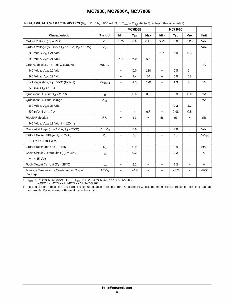
MC7800, MC7800A, NCV7805
http://onsemi.com5
ELECTRICAL CHARACTERISTICS (Vin = 11 V, IO = 500 mA, TJ = Tlow to Thigh (Note 5), unless otherwise noted)
MC7806B MC7806C
Characteristic Symbol Min Typ Max Min Typ Max Unit
Output Voltage (TJ = 25°C) VO 5.75 6.0 6.25 5.75 6.0 6.25 Vdc
Output Voltage (5.0 mA ≤ IO ≤ 1.0 A, PD ≤ 15 W) VO Vdc
8.0 Vdc ≤ Vin ≤ 21 Vdc − − − 5.7 6.0 6.3
9.0 Vdc ≤ Vin ≤ 21 Vdc 5.7 6.0 6.3 − − −
Line Regulation, TJ = 25°C (Note 6) Regline mV
8.0 Vdc ≤ Vin ≤ 25 Vdc − 5.5 120 − 0.5 24
9.0 Vdc ≤ Vin ≤ 13 Vdc − 1.4 60 − 0.8 12
Load Regulation, TJ = 25°C (Note 6) Regload − 1.3 120 − 1.3 30 mV
5.0 mA ≤ IO ≤ 1.5 A
Quiescent Current (TJ = 25°C) IB − 3.3 8.0 − 3.3 8.0 mA
Quiescent Current Change IB mA
8.0 Vdc ≤ Vin ≤ 25 Vdc − − − − 0.3 1.3
5.0 mA ≤ IO ≤ 1.0 A − − 0.5 − 0.08 0.5
Ripple Rejection RR − 65 − 58 65 − dB
9.0 Vdc ≤ Vin ≤ 19 Vdc, f = 120 Hz
Dropout Voltage (IO = 1.0 A, TJ = 25°C) VI − VO − 2.0 − − 2.0 − Vdc
Output Noise Voltage (TA = 25°C) Vn − 10 − − 10 − V/VO
10 Hz ≤ f ≤ 100 kHz
Output Resistance f = 1.0 kHz rO − 0.9 − − 0.9 − m
Short Circuit Current Limit (TA = 25°C) ISC − 0.2 − − 0.2 − A
Vin = 35 Vdc
Peak Output Current (TJ = 25°C) Imax − 2.2 − − 2.2 − A
Average Temperature Coefficient of OutputVoltage
TCVO − −0.3 − − −0.3 − mV/°C
5. Tlow = 0°C for MC78XXAC, C Thigh = +125°C for MC78XXAC, NCV7805= −40°C for MC78XXB, MC78XXAB, NCV7805
6. Load and line regulation are specified at constant junction temperature. Changes in VO due to heating effects must be taken into accountseparately. Pulse testing with low duty cycle is used.
MC7800, MC7800A, NCV7805
http://onsemi.com6
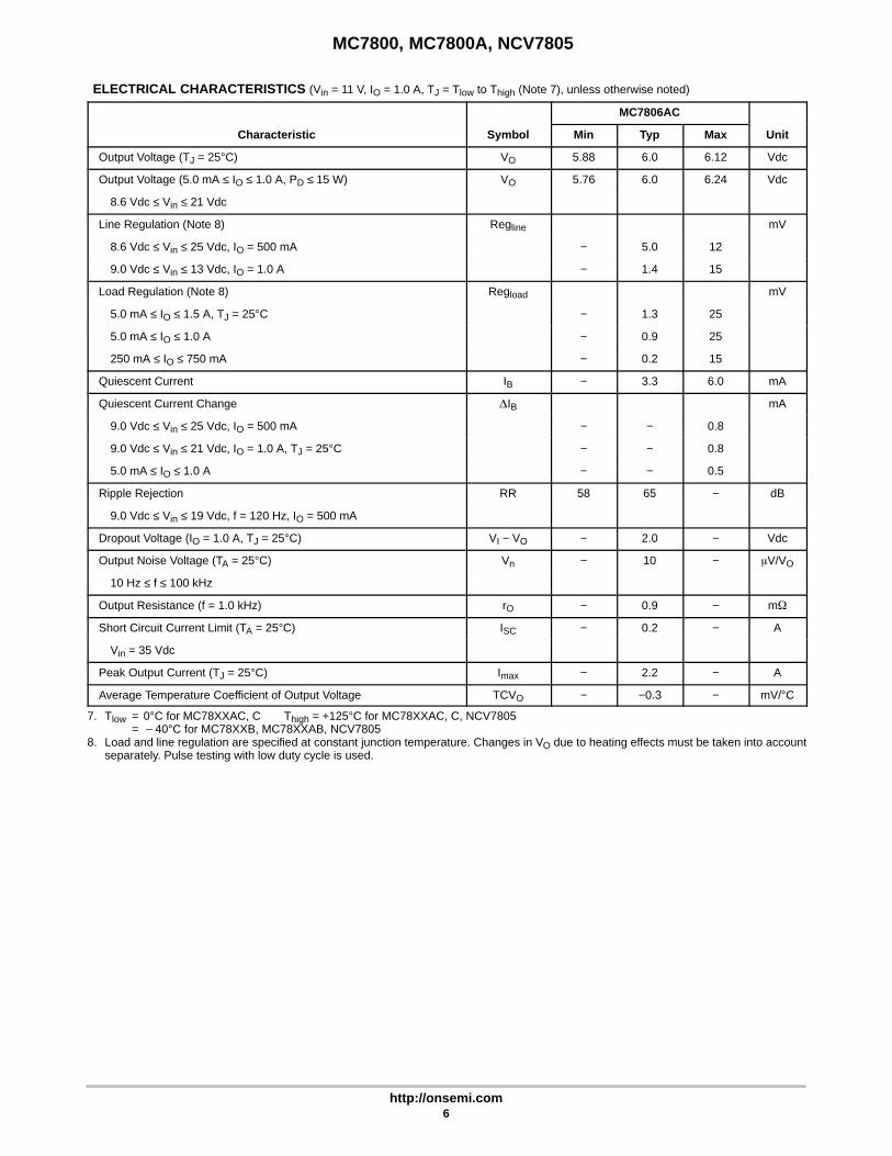
ELECTRICAL CHARACTERISTICS (Vin = 11 V, IO = 1.0 A, TJ = Tlow to Thigh (Note 7), unless otherwise noted)
MC7806AC
Characteristic Symbol Min Typ Max Unit
Output Voltage (TJ = 25°C) VO 5.88 6.0 6.12 Vdc
Output Voltage (5.0 mA ≤ IO ≤ 1.0 A, PD ≤ 15 W) VO 5.76 6.0 6.24 Vdc
8.6 Vdc ≤ Vin ≤ 21 Vdc
Line Regulation (Note 8) Regline mV
8.6 Vdc ≤ Vin ≤ 25 Vdc, IO = 500 mA − 5.0 12
9.0 Vdc ≤ Vin ≤ 13 Vdc, IO = 1.0 A − 1.4 15
Load Regulation (Note 8) Regload mV
5.0 mA ≤ IO ≤ 1.5 A, TJ = 25°C − 1.3 25
5.0 mA ≤ IO ≤ 1.0 A − 0.9 25
250 mA ≤ IO ≤ 750 mA − 0.2 15
Quiescent Current IB − 3.3 6.0 mA
Quiescent Current Change IB mA
9.0 Vdc ≤ Vin ≤ 25 Vdc, IO = 500 mA − − 0.8
9.0 Vdc ≤ Vin ≤ 21 Vdc, IO = 1.0 A, TJ = 25°C − − 0.8
5.0 mA ≤ IO ≤ 1.0 A − − 0.5
Ripple Rejection RR 58 65 − dB
9.0 Vdc ≤ Vin ≤ 19 Vdc, f = 120 Hz, IO = 500 mA
Dropout Voltage (IO = 1.0 A, TJ = 25°C) VI − VO − 2.0 − Vdc
Output Noise Voltage (TA = 25°C) Vn − 10 − V/VO
10 Hz ≤ f ≤ 100 kHz
Output Resistance (f = 1.0 kHz) rO − 0.9 − m
Short Circuit Current Limit (TA = 25°C) ISC − 0.2 − A
Vin = 35 Vdc
Peak Output Current (TJ = 25°C) Imax − 2.2 − A
Average Temperature Coefficient of Output Voltage TCVO − −0.3 − mV/°C
7. Tlow = 0°C for MC78XXAC, C Thigh = +125°C for MC78XXAC, C, NCV7805= 40°C for MC78XXB, MC78XXAB, NCV7805
8. Load and line regulation are specified at constant junction temperature. Changes in VO due to heating effects must be taken into accountseparately. Pulse testing with low duty cycle is used.
MC7800, MC7800A, NCV7805
http://onsemi.com7
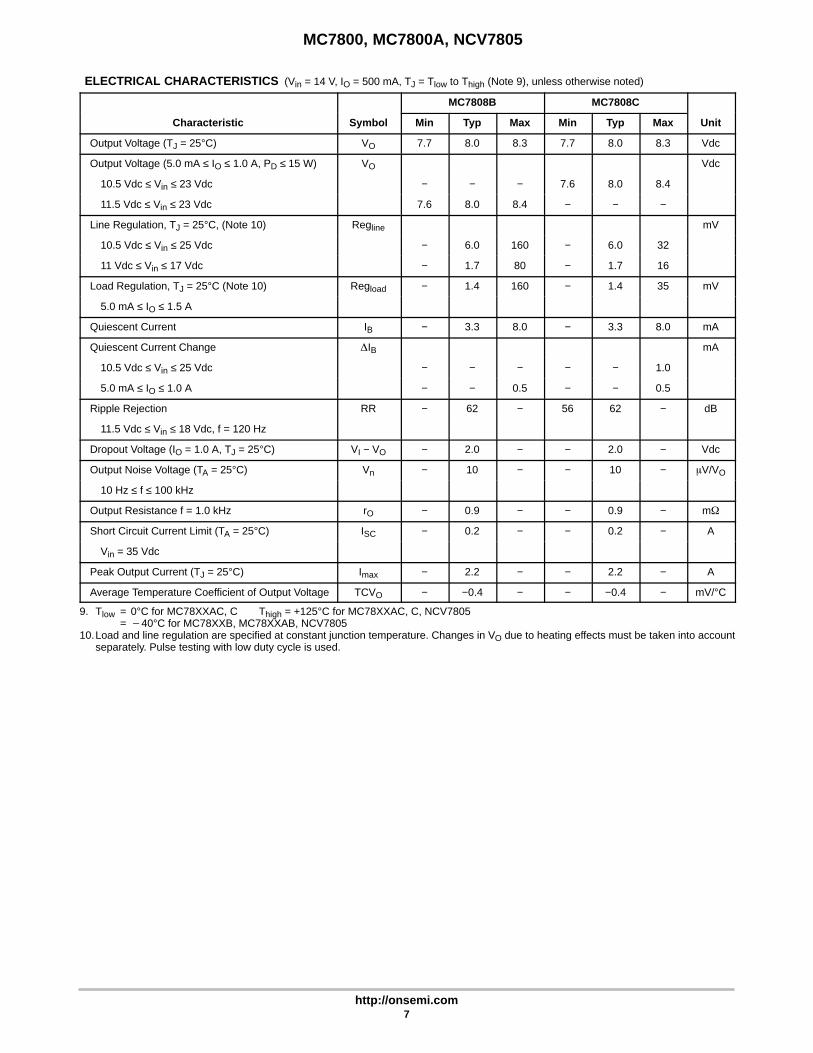
ELECTRICAL CHARACTERISTICS (Vin = 14 V, IO = 500 mA, TJ = Tlow to Thigh (Note 9), unless otherwise noted)
MC7808B MC7808C
Characteristic Symbol Min Typ Max Min Typ Max Unit
Output Voltage (TJ = 25°C) VO 7.7 8.0 8.3 7.7 8.0 8.3 Vdc
Output Voltage (5.0 mA ≤ IO ≤ 1.0 A, PD ≤ 15 W) VO Vdc
10.5 Vdc ≤ Vin ≤ 23 Vdc − − − 7.6 8.0 8.4
11.5 Vdc ≤ Vin ≤ 23 Vdc 7.6 8.0 8.4 − − −
Line Regulation, TJ = 25°C, (Note 10) Regline mV
10.5 Vdc ≤ Vin ≤ 25 Vdc − 6.0 160 − 6.0 32
11 Vdc ≤ Vin ≤ 17 Vdc − 1.7 80 − 1.7 16
Load Regulation, TJ = 25°C (Note 10) Regload − 1.4 160 − 1.4 35 mV
5.0 mA ≤ IO ≤ 1.5 A
Quiescent Current IB − 3.3 8.0 − 3.3 8.0 mA
Quiescent Current Change IB mA
10.5 Vdc ≤ Vin ≤ 25 Vdc − − − − − 1.0
5.0 mA ≤ IO ≤ 1.0 A − − 0.5 − − 0.5
Ripple Rejection RR − 62 − 56 62 − dB
11.5 Vdc ≤ Vin ≤ 18 Vdc, f = 120 Hz
Dropout Voltage (IO = 1.0 A, TJ = 25°C) VI − VO − 2.0 − − 2.0 − Vdc
Output Noise Voltage (TA = 25°C) Vn − 10 − − 10 − V/VO
10 Hz ≤ f ≤ 100 kHz
Output Resistance f = 1.0 kHz rO − 0.9 − − 0.9 − m
Short Circuit Current Limit (TA = 25°C) ISC − 0.2 − − 0.2 − A
Vin = 35 Vdc
Peak Output Current (TJ = 25°C) Imax − 2.2 − − 2.2 − A
Average Temperature Coefficient of Output Voltage TCVO − −0.4 − − −0.4 − mV/°C
9. Tlow = 0°C for MC78XXAC, C Thigh = +125°C for MC78XXAC, C, NCV7805= 40°C for MC78XXB, MC78XXAB, NCV7805
10.Load and line regulation are specified at constant junction temperature. Changes in VO due to heating effects must be taken into accountseparately. Pulse testing with low duty cycle is used.
MC7800, MC7800A, NCV7805
http://onsemi.com8
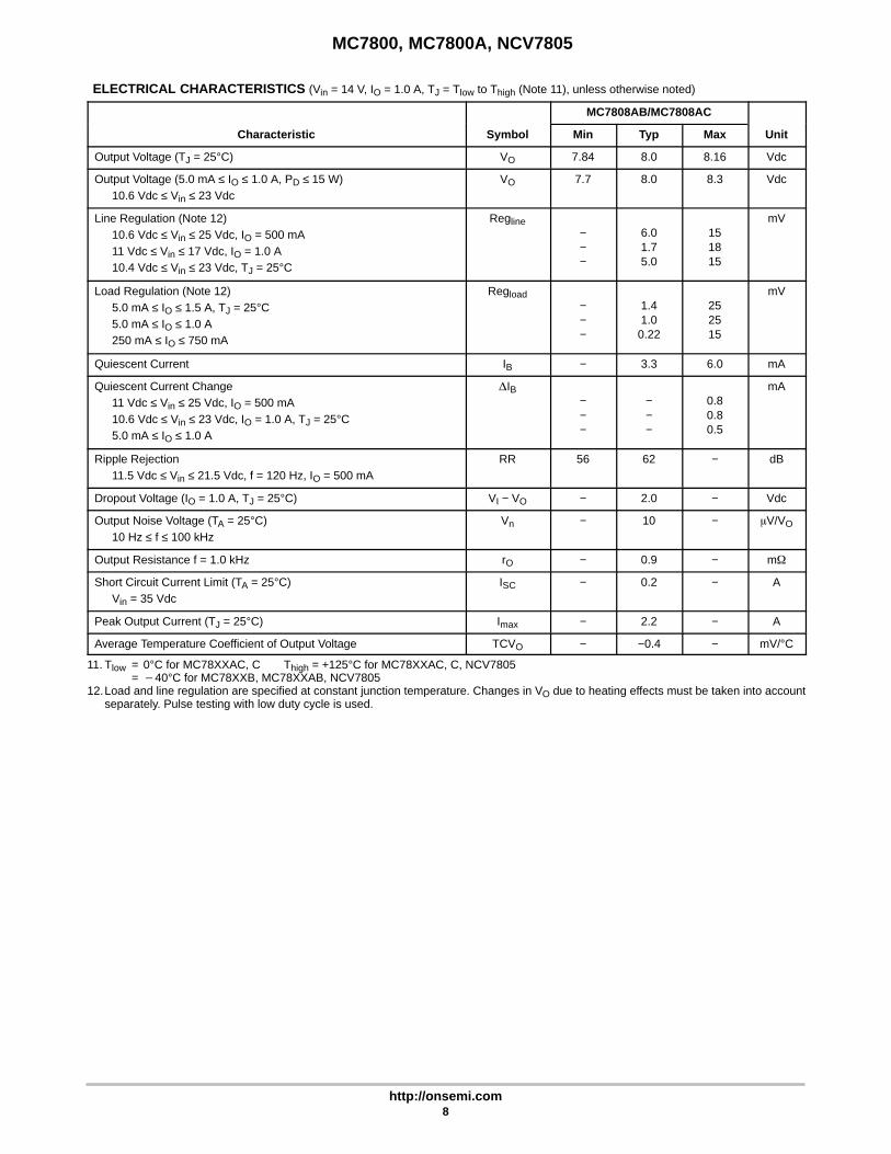
ELECTRICAL CHARACTERISTICS (Vin = 14 V, IO = 1.0 A, TJ = Tlow to Thigh (Note 11), unless otherwise noted)
MC7808AB/MC7808AC
Characteristic Symbol Min Typ Max Unit
Output Voltage (TJ = 25°C) VO 7.84 8.0 8.16 Vdc
Output Voltage (5.0 mA ≤ IO ≤ 1.0 A, PD ≤ 15 W)10.6 Vdc ≤ Vin ≤ 23 Vdc
VO 7.7 8.0 8.3 Vdc
Line Regulation (Note 12)10.6 Vdc ≤ Vin ≤ 25 Vdc, IO = 500 mA11 Vdc ≤ Vin ≤ 17 Vdc, IO = 1.0 A10.4 Vdc ≤ Vin ≤ 23 Vdc, TJ = 25°C
Regline−−−
6.01.75.0
151815
mV
Load Regulation (Note 12)5.0 mA ≤ IO ≤ 1.5 A, TJ = 25°C5.0 mA ≤ IO ≤ 1.0 A250 mA ≤ IO ≤ 750 mA
Regload−−−
1.41.00.22
252515
mV
Quiescent Current IB − 3.3 6.0 mA
Quiescent Current Change11 Vdc ≤ Vin ≤ 25 Vdc, IO = 500 mA10.6 Vdc ≤ Vin ≤ 23 Vdc, IO = 1.0 A, TJ = 25°C5.0 mA ≤ IO ≤ 1.0 A
IB−−−
−−−
0.80.80.5
mA
Ripple Rejection11.5 Vdc ≤ Vin ≤ 21.5 Vdc, f = 120 Hz, IO = 500 mA
RR 56 62 − dB
Dropout Voltage (IO = 1.0 A, TJ = 25°C) VI − VO − 2.0 − Vdc
Output Noise Voltage (TA = 25°C)10 Hz ≤ f ≤ 100 kHz
Vn − 10 − V/VO
Output Resistance f = 1.0 kHz rO − 0.9 − m
Short Circuit Current Limit (TA = 25°C)Vin = 35 Vdc
ISC − 0.2 − A
Peak Output Current (TJ = 25°C) Imax − 2.2 − A
Average Temperature Coefficient of Output Voltage TCVO − −0.4 − mV/°C
11. Tlow = 0°C for MC78XXAC, C Thigh = +125°C for MC78XXAC, C, NCV7805= 40°C for MC78XXB, MC78XXAB, NCV7805
12.Load and line regulation are specified at constant junction temperature. Changes in VO due to heating effects must be taken into accountseparately. Pulse testing with low duty cycle is used.
MC7800, MC7800A, NCV7805
http://onsemi.com9
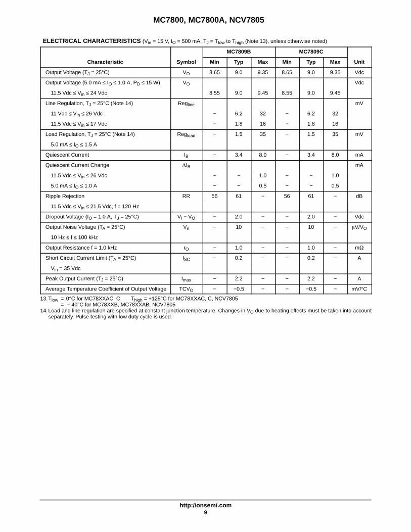
ELECTRICAL CHARACTERISTICS (Vin = 15 V, IO = 500 mA, TJ = Tlow to Thigh (Note 13), unless otherwise noted)
MC7809B MC7809C
Characteristic Symbol Min Typ Max Min Typ Max Unit
Output Voltage (TJ = 25°C) VO 8.65 9.0 9.35 8.65 9.0 9.35 Vdc
Output Voltage (5.0 mA ≤ IO ≤ 1.0 A, PD ≤ 15 W) VO Vdc
11.5 Vdc ≤ Vin ≤ 24 Vdc 8.55 9.0 9.45 8.55 9.0 9.45
Line Regulation, TJ = 25°C (Note 14) Regline mV
11 Vdc ≤ Vin ≤ 26 Vdc − 6.2 32 − 6.2 32
11.5 Vdc ≤ Vin ≤ 17 Vdc − 1.8 16 − 1.8 16
Load Regulation, TJ = 25°C (Note 14) Regload − 1.5 35 − 1.5 35 mV
5.0 mA ≤ IO ≤ 1.5 A
Quiescent Current IB − 3.4 8.0 − 3.4 8.0 mA
Quiescent Current Change IB mA
11.5 Vdc ≤ Vin ≤ 26 Vdc − − 1.0 − − 1.0
5.0 mA ≤ IO ≤ 1.0 A − − 0.5 − − 0.5
Ripple Rejection RR 56 61 − 56 61 − dB
11.5 Vdc ≤ Vin ≤ 21.5 Vdc, f = 120 Hz
Dropout Voltage (IO = 1.0 A, TJ = 25°C) VI − VO − 2.0 − − 2.0 − Vdc
Output Noise Voltage (TA = 25°C) Vn − 10 − − 10 − V/VO
10 Hz ≤ f ≤ 100 kHz
Output Resistance f = 1.0 kHz rO − 1.0 − − 1.0 − m
Short Circuit Current Limit (TA = 25°C) ISC − 0.2 − − 0.2 − A
Vin = 35 Vdc
Peak Output Current (TJ = 25°C) Imax − 2.2 − − 2.2 − A
Average Temperature Coefficient of Output Voltage TCVO − −0.5 − − −0.5 − mV/°C
13.Tlow = 0°C for MC78XXAC, C Thigh = +125°C for MC78XXAC, C, NCV7805= 40°C for MC78XXB, MC78XXAB, NCV7805
14.Load and line regulation are specified at constant junction temperature. Changes in VO due to heating effects must be taken into accountseparately. Pulse testing with low duty cycle is used.
MC7800, MC7800A, NCV7805
http://onsemi.com10
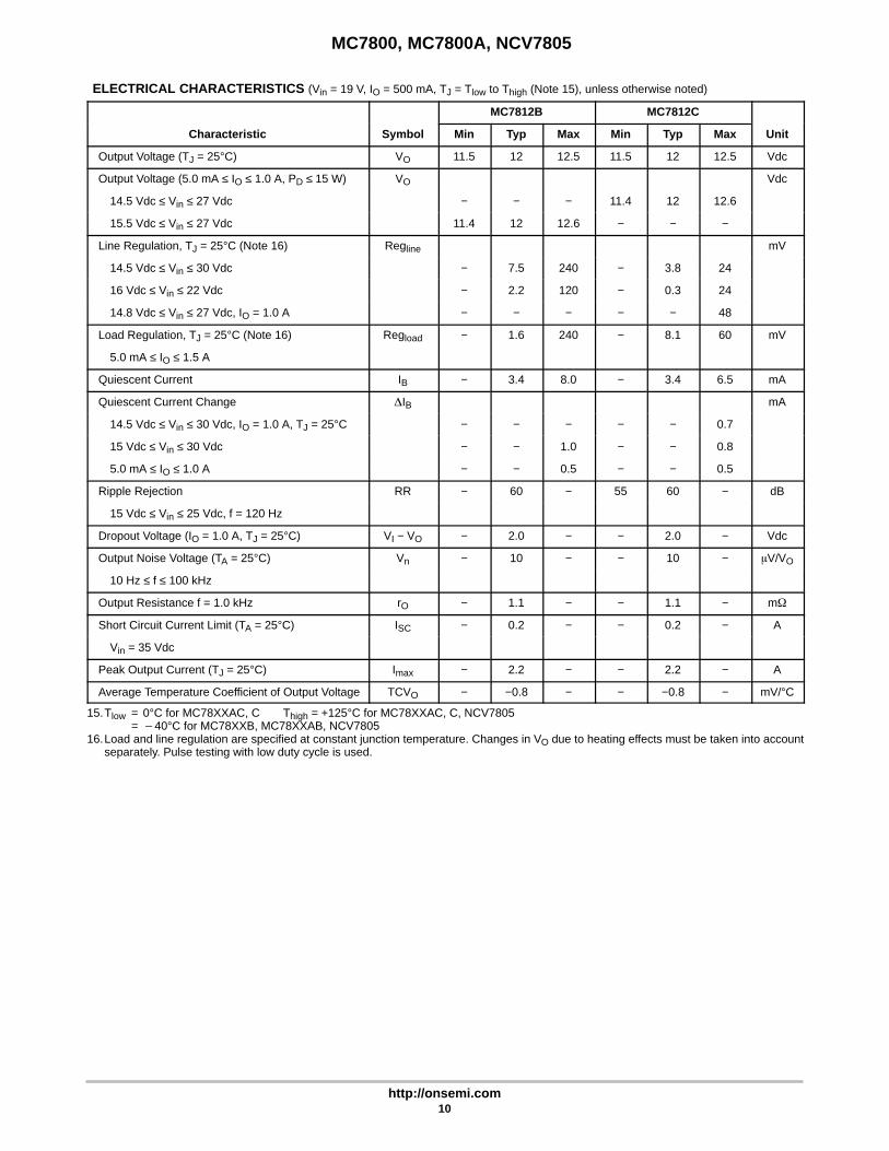
ELECTRICAL CHARACTERISTICS (Vin = 19 V, IO = 500 mA, TJ = Tlow to Thigh (Note 15), unless otherwise noted)
MC7812B MC7812C
Characteristic Symbol Min Typ Max Min Typ Max Unit
Output Voltage (TJ = 25°C) VO 11.5 12 12.5 11.5 12 12.5 Vdc
Output Voltage (5.0 mA ≤ IO ≤ 1.0 A, PD ≤ 15 W) VO Vdc
14.5 Vdc ≤ Vin ≤ 27 Vdc − − − 11.4 12 12.6
15.5 Vdc ≤ Vin ≤ 27 Vdc 11.4 12 12.6 − − −
Line Regulation, TJ = 25°C (Note 16) Regline mV
14.5 Vdc ≤ Vin ≤ 30 Vdc − 7.5 240 − 3.8 24
16 Vdc ≤ Vin ≤ 22 Vdc − 2.2 120 − 0.3 24
14.8 Vdc ≤ Vin ≤ 27 Vdc, IO = 1.0 A − − − − − 48
Load Regulation, TJ = 25°C (Note 16) Regload − 1.6 240 − 8.1 60 mV
5.0 mA ≤ IO ≤ 1.5 A
Quiescent Current IB − 3.4 8.0 − 3.4 6.5 mA
Quiescent Current Change IB mA
14.5 Vdc ≤ Vin ≤ 30 Vdc, IO = 1.0 A, TJ = 25°C − − − − − 0.7
15 Vdc ≤ Vin ≤ 30 Vdc − − 1.0 − − 0.8
5.0 mA ≤ IO ≤ 1.0 A − − 0.5 − − 0.5
Ripple Rejection RR − 60 − 55 60 − dB
15 Vdc ≤ Vin ≤ 25 Vdc, f = 120 Hz
Dropout Voltage (IO = 1.0 A, TJ = 25°C) VI − VO − 2.0 − − 2.0 − Vdc
Output Noise Voltage (TA = 25°C) Vn − 10 − − 10 − V/VO
10 Hz ≤ f ≤ 100 kHz
Output Resistance f = 1.0 kHz rO − 1.1 − − 1.1 − m
Short Circuit Current Limit (TA = 25°C) ISC − 0.2 − − 0.2 − A
Vin = 35 Vdc
Peak Output Current (TJ = 25°C) Imax − 2.2 − − 2.2 − A
Average Temperature Coefficient of Output Voltage TCVO − −0.8 − − −0.8 − mV/°C
15.Tlow = 0°C for MC78XXAC, C Thigh = +125°C for MC78XXAC, C, NCV7805= 40°C for MC78XXB, MC78XXAB, NCV7805
16.Load and line regulation are specified at constant junction temperature. Changes in VO due to heating effects must be taken into accountseparately. Pulse testing with low duty cycle is used.

MC7800, MC7800A, NCV7805
http://onsemi.com11
ELECTRICAL CHARACTERISTICS (Vin = 19 V, IO = 1.0 A, TJ = Tlow to Thigh (Note 17), unless otherwise noted)
MC7812AB/MC7812AC
Characteristic Symbol Min Typ Max Unit
Output Voltage (TJ = 25°C) VO 11.75 12 12.25 Vdc
Output Voltage (5.0 mA ≤ IO ≤ 1.0 A, PD ≤ 15 W) VO 11.5 12 12.5 Vdc
14.8 Vdc ≤ Vin ≤ 27 Vdc
Line Regulation (Note 18) Regline mV
14.8 Vdc ≤ Vin ≤ 30 Vdc, IO = 500 mA − 3.8 18
16 Vdc ≤ Vin ≤ 22 Vdc, IO = 1.0 A − 2.2 20
14.5 Vdc ≤ Vin ≤ 27 Vdc, TJ = 25°C − 6.0 120
Load Regulation (Note 18) Regload mV
5.0 mA ≤ IO ≤ 1.5 A, TJ = 25°C − − 25
5.0 mA ≤ IO ≤ 1.0 A − − 25
Quiescent Current IB − 3.4 6.0 mA
Quiescent Current Change IB mA
15 Vdc ≤ Vin ≤ 30 Vdc, IO = 500 mA − − 0.8
14.8 Vdc ≤ Vin ≤ 27 Vdc, TJ = 25°C − − 0.8
5.0 mA ≤ IO ≤ 1.0 A, TJ = 25°C − − 0.5
Ripple Rejection RR 55 60 − dB
15 Vdc ≤ Vin ≤ 25 Vdc, f = 120 Hz, IO = 500 mA
Dropout Voltage (IO = 1.0 A, TJ = 25°C) VI − VO − 2.0 − Vdc
Output Noise Voltage (TA = 25°C) Vn − 10 − V/VO
10 Hz ≤ f ≤ 100 kHz
Output Resistance (f = 1.0 kHz) rO − 1.1 − m
Short Circuit Current Limit (TA = 25°C) ISC − 0.2 − A
Vin = 35 Vdc
Peak Output Current (TJ = 25°C) Imax − 2.2 − A
Average Temperature Coefficient of Output Voltage TCVO − −0.8 − mV/°C
17.Tlow = 0°C for MC78XXAC, C Thigh = +125°C for MC78XXAC, C, NCV7805= 40°C for MC78XXB, MC78XXAB, NCV7805
18.Load and line regulation are specified at constant junction temperature. Changes in VO due to heating effects must be taken into accountseparately. Pulse testing with low duty cycle is used.
MC7800, MC7800A, NCV7805
http://onsemi.com12
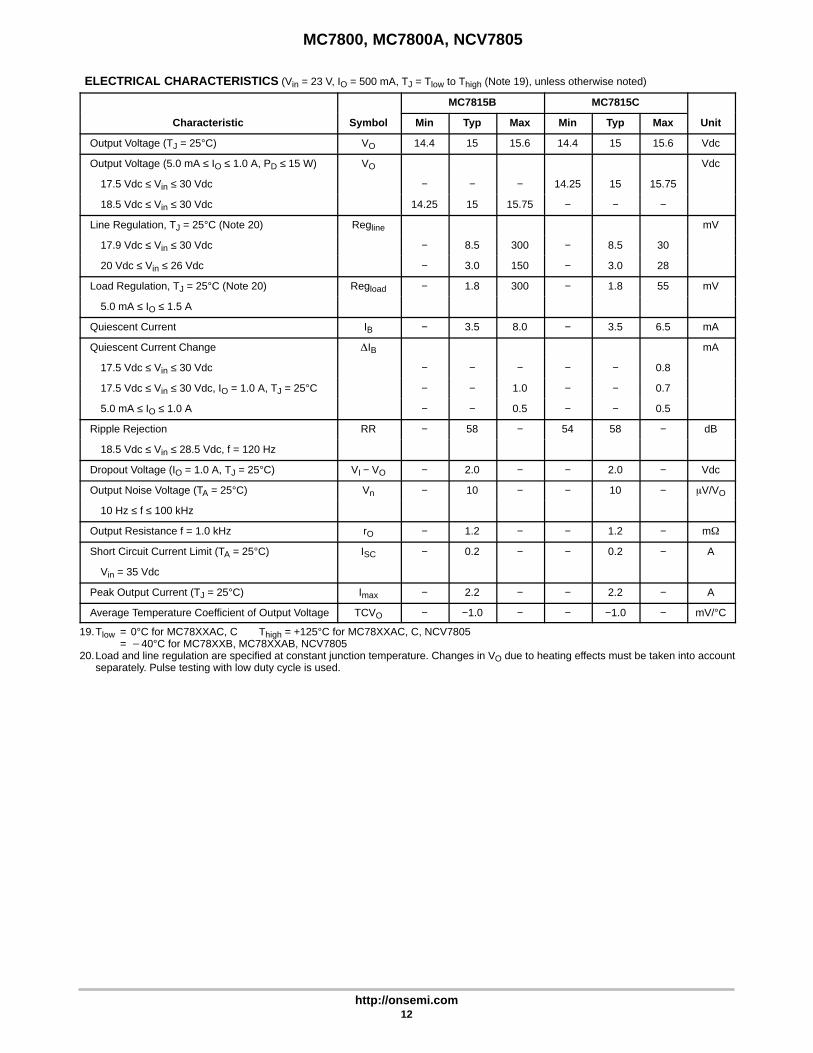
ELECTRICAL CHARACTERISTICS (Vin = 23 V, IO = 500 mA, TJ = Tlow to Thigh (Note 19), unless otherwise noted)
MC7815B MC7815C
Characteristic Symbol Min Typ Max Min Typ Max Unit
Output Voltage (TJ = 25°C) VO 14.4 15 15.6 14.4 15 15.6 Vdc
Output Voltage (5.0 mA ≤ IO ≤ 1.0 A, PD ≤ 15 W) VO Vdc
17.5 Vdc ≤ Vin ≤ 30 Vdc − − − 14.25 15 15.75
18.5 Vdc ≤ Vin ≤ 30 Vdc 14.25 15 15.75 − − −
Line Regulation, TJ = 25°C (Note 20) Regline mV
17.9 Vdc ≤ Vin ≤ 30 Vdc − 8.5 300 − 8.5 30
20 Vdc ≤ Vin ≤ 26 Vdc − 3.0 150 − 3.0 28
Load Regulation, TJ = 25°C (Note 20) Regload − 1.8 300 − 1.8 55 mV
5.0 mA ≤ IO ≤ 1.5 A
Quiescent Current IB − 3.5 8.0 − 3.5 6.5 mA
Quiescent Current Change IB mA
17.5 Vdc ≤ Vin ≤ 30 Vdc − − − − − 0.8
17.5 Vdc ≤ Vin ≤ 30 Vdc, IO = 1.0 A, TJ = 25°C − − 1.0 − − 0.7
5.0 mA ≤ IO ≤ 1.0 A − − 0.5 − − 0.5
Ripple Rejection RR − 58 − 54 58 − dB
18.5 Vdc ≤ Vin ≤ 28.5 Vdc, f = 120 Hz
Dropout Voltage (IO = 1.0 A, TJ = 25°C) VI − VO − 2.0 − − 2.0 − Vdc
Output Noise Voltage (TA = 25°C) Vn − 10 − − 10 − V/VO
10 Hz ≤ f ≤ 100 kHz
Output Resistance f = 1.0 kHz rO − 1.2 − − 1.2 − m
Short Circuit Current Limit (TA = 25°C) ISC − 0.2 − − 0.2 − A
Vin = 35 Vdc
Peak Output Current (TJ = 25°C) Imax − 2.2 − − 2.2 − A
Average Temperature Coefficient of Output Voltage TCVO − −1.0 − − −1.0 − mV/°C
19.Tlow = 0°C for MC78XXAC, C Thigh = +125°C for MC78XXAC, C, NCV7805= 40°C for MC78XXB, MC78XXAB, NCV7805
20.Load and line regulation are specified at constant junction temperature. Changes in VO due to heating effects must be taken into accountseparately. Pulse testing with low duty cycle is used.
MC7800, MC7800A, NCV7805
http://onsemi.com13
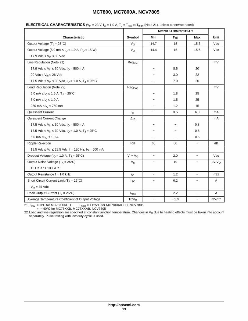
ELECTRICAL CHARACTERISTICS (Vin = 23 V, IO = 1.0 A, TJ = Tlow to Thigh (Note 21), unless otherwise noted)
MC7815AB/MC7815AC
Characteristic Symbol Min Typ Max Unit
Output Voltage (TJ = 25°C) VO 14.7 15 15.3 Vdc
Output Voltage (5.0 mA ≤ IO ≤ 1.0 A, PD ≤ 15 W) VO 14.4 15 15.6 Vdc
17.9 Vdc ≤ Vin ≤ 30 Vdc
Line Regulation (Note 22) Regline mV
17.9 Vdc ≤ Vin ≤ 30 Vdc, IO = 500 mA − 8.5 20
20 Vdc ≤ Vin ≤ 26 Vdc − 3.0 22
17.5 Vdc ≤ Vin ≤ 30 Vdc, IO = 1.0 A, TJ = 25°C − 7.0 20
Load Regulation (Note 22) Regload mV
5.0 mA ≤ IO ≤ 1.5 A, TJ = 25°C − 1.8 25
5.0 mA ≤ IO ≤ 1.0 A − 1.5 25
250 mA ≤ IO ≤ 750 mA − 1.2 15
Quiescent Current IB − 3.5 6.0 mA
Quiescent Current Change IB mA
17.5 Vdc ≤ Vin ≤ 30 Vdc, IO = 500 mA − − 0.8
17.5 Vdc ≤ Vin ≤ 30 Vdc, IO = 1.0 A, TJ = 25°C − − 0.8
5.0 mA ≤ IO ≤ 1.0 A − − 0.5
Ripple Rejection RR 60 80 − dB
18.5 Vdc ≤ Vin ≤ 28.5 Vdc, f = 120 Hz, IO = 500 mA
Dropout Voltage (IO = 1.0 A, TJ = 25°C) VI − VO − 2.0 − Vdc
Output Noise Voltage (TA = 25°C) Vn − 10 − V/VO
10 Hz ≤ f ≤ 100 kHz
Output Resistance f = 1.0 kHz rO − 1.2 − m
Short Circuit Current Limit (TA = 25°C) ISC − 0.2 − A
Vin = 35 Vdc
Peak Output Current (TJ = 25°C) Imax − 2.2 − A
Average Temperature Coefficient of Output Voltage TCVO − −1.0 − mV/°C
21.Tlow = 0°C for MC78XXAC, C Thigh = +125°C for MC78XXAC, C, NCV7805= 40°C for MC78XXB, MC78XXAB, NCV7805
22.Load and line regulation are specified at constant junction temperature. Changes in VO due to heating effects must be taken into accountseparately. Pulse testing with low duty cycle is used.
MC7800, MC7800A, NCV7805
http://onsemi.com14
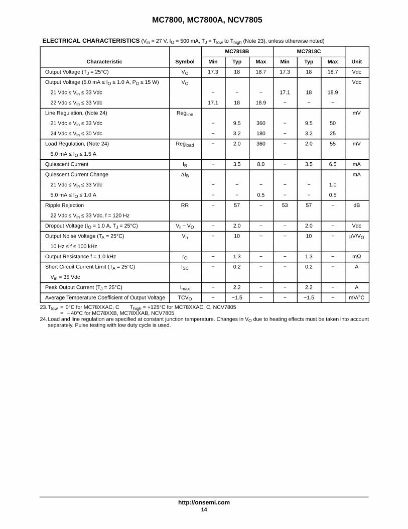
ELECTRICAL CHARACTERISTICS (Vin = 27 V, IO = 500 mA, TJ = Tlow to Thigh (Note 23), unless otherwise noted)
MC7818B MC7818C
Characteristic Symbol Min Typ Max Min Typ Max Unit
Output Voltage (TJ = 25°C) VO 17.3 18 18.7 17.3 18 18.7 Vdc
Output Voltage (5.0 mA ≤ IO ≤ 1.0 A, PD ≤ 15 W) VO Vdc
21 Vdc ≤ Vin ≤ 33 Vdc − − − 17.1 18 18.9
22 Vdc ≤ Vin ≤ 33 Vdc 17.1 18 18.9 − − −
Line Regulation, (Note 24) Regline mV
21 Vdc ≤ Vin ≤ 33 Vdc − 9.5 360 − 9.5 50
24 Vdc ≤ Vin ≤ 30 Vdc − 3.2 180 − 3.2 25
Load Regulation, (Note 24) Regload − 2.0 360 − 2.0 55 mV
5.0 mA ≤ IO ≤ 1.5 A
Quiescent Current IB − 3.5 8.0 − 3.5 6.5 mA
Quiescent Current Change IB mA
21 Vdc ≤ Vin ≤ 33 Vdc − − − − − 1.0
5.0 mA ≤ IO ≤ 1.0 A − − 0.5 − − 0.5
Ripple Rejection RR − 57 − 53 57 − dB
22 Vdc ≤ Vin ≤ 33 Vdc, f = 120 Hz
Dropout Voltage (IO = 1.0 A, TJ = 25°C) ViI − VO − 2.0 − − 2.0 − Vdc
Output Noise Voltage (TA = 25°C) Vn − 10 − − 10 − V/VO
10 Hz ≤ f ≤ 100 kHz
Output Resistance f = 1.0 kHz rO − 1.3 − − 1.3 − m
Short Circuit Current Limit (TA = 25°C) ISC − 0.2 − − 0.2 − A
Vin = 35 Vdc
Peak Output Current (TJ = 25°C) Imax − 2.2 − − 2.2 − A
Average Temperature Coefficient of Output Voltage TCVO − −1.5 − − −1.5 − mV/°C
23.Tlow = 0°C for MC78XXAC, C Thigh = +125°C for MC78XXAC, C, NCV7805= 40°C for MC78XXB, MC78XXAB, NCV7805
24.Load and line regulation are specified at constant junction temperature. Changes in VO due to heating effects must be taken into accountseparately. Pulse testing with low duty cycle is used.
MC7800, MC7800A, NCV7805
http://onsemi.com15
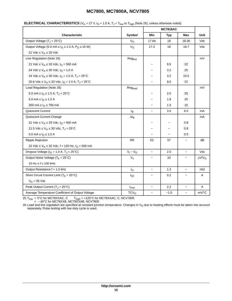
ELECTRICAL CHARACTERISTICS (Vin = 27 V, IO = 1.0 A, TJ = Tlow to Thigh (Note 25), unless otherwise noted)
MC7818AC
Characteristic Symbol Min Typ Max Unit
Output Voltage (TJ = 25°C) VO 17.64 18 18.36 Vdc
Output Voltage (5.0 mA ≤ IO ≤ 1.0 A, PD ≤ 15 W) VO 17.3 18 18.7 Vdc
21 Vdc ≤ Vin ≤ 33 Vdc
Line Regulation (Note 26) Regline mV
21 Vdc ≤ Vin ≤ 33 Vdc, IO = 500 mA − 9.5 22
24 Vdc ≤ Vin ≤ 30 Vdc, IO = 1.0 A − 3.2 25
24 Vdc ≤ Vin ≤ 30 Vdc, IO = 1.0 A, TJ = 25°C − 3.2 10.5
20.6 Vdc ≤ Vin ≤ 33 Vdc, IO = 1.0 A, TJ = 25°C − 8.0 22
Load Regulation (Note 26) Regload mV
5.0 mA ≤ IO ≤ 1.5 A, TJ = 25°C − 2.0 25
5.0 mA ≤ IO ≤ 1.0 A − 1.8 25
250 mA ≤ IO ≤ 750 mA − 1.5 15
Quiescent Current IB − 3.5 6.0 mA
Quiescent Current Change IB mA
21 Vdc ≤ Vin ≤ 33 Vdc, IO = 500 mA − − 0.8
21.5 Vdc ≤ Vin ≤ 30 Vdc, TJ = 25°C − − 0.8
5.0 mA ≤ IO ≤ 1.0 A − − 0.5
Ripple Rejection RR 53 57 − dB
22 Vdc ≤ Vin ≤ 32 Vdc, f = 120 Hz, IO = 500 mA
Dropout Voltage (IO = 1.0 A, TJ = 25°C) VI − VO − 2.0 − Vdc
Output Noise Voltage (TA = 25°C) Vn − 10 − V/VO
10 Hz ≤ f ≤ 100 kHz
Output Resistance f = 1.0 kHz rO − 1.3 − m
Short Circuit Current Limit (TA = 25°C) ISC − 0.2 − A
Vin = 35 Vdc
Peak Output Current (TJ = 25°C) Imax − 2.2 − A
Average Temperature Coefficient of Output Voltage TCVO − −1.5 − mV/°C
25.Tlow = 0°C for MC78XXAC, C Thigh = +125°C for MC78XXAC, C, NCV7805= 40°C for MC78XXB, MC78XXAB, NCV7805
26.Load and line regulation are specified at constant junction temperature. Changes in VO due to heating effects must be taken into accountseparately. Pulse testing with low duty cycle is used.

MC7800, MC7800A, NCV7805
http://onsemi.com16
ELECTRICAL CHARACTERISTICS (Vin = 33 V, IO = 500 mA, TJ = Tlow to Thigh (Note 27), unless otherwise noted)
MC7824B MC7824C
Characteristic Symbol Min Typ Max Min Typ Max Unit
Output Voltage (TJ = 25°C) VO 23 24 25 23 24 25 Vdc
Output Voltage (5.0 mA ≤ IO ≤ 1.0 A, PD ≤ 15 W) VO Vdc
27 Vdc ≤ Vin ≤ 38 Vdc − − − 22.8 24 25.2
28 Vdc ≤ Vin ≤ 38 Vdc 22.8 24 25.2 − − −
Line Regulation, (Note 28) Regline mV
27 Vdc ≤ Vin ≤ 38 Vdc − 11.5 480 − 2.7 60
30 Vdc ≤ Vin ≤ 36 Vdc − 3.8 240 − 2.7 48
Load Regulation, (Note 28) Regload − 2.1 480 − 4.4 65 mV
5.0 mA ≤ IO ≤ 1.5 A
Quiescent Current IB − 3.6 8.0 − 3.6 6.5 mA
Quiescent Current Change IB mA
27 Vdc ≤ Vin ≤ 38 Vdc − − − − − 1.0
5.0 mA ≤ IO ≤ 1.0 A − − 0.5 − − 0.5
Ripple Rejection RR − 54 − 50 54 − dB
28 Vdc ≤ Vin ≤ 38 Vdc, f = 120 Hz
Dropout Voltage (IO = 1.0 A, TJ = 25°C) VI − VO − 2.0 − − 2.0 − Vdc
Output Noise Voltage (TA = 25°C) Vn − 10 − − 10 − V/VO
10 Hz ≤ f ≤ 100 kHz
Output Resistance f = 1.0 kHz rO − 1.4 − − 1.4 − m
Short Circuit Current Limit (TA = 25°C) ISC − 0.2 − − 0.2 − A
Vin = 35 Vdc
Peak Output Current (TJ = 25°C) Imax − 2.2 − − 2.2 − A
Average Temperature Coefficient of Output Voltage TCVO − −2.0 − − −2.0 − mV/°C
27.Tlow = 0°C for MC78XXAC, C Thigh = +125°C for MC78XXAC, C, NCV7805= 40°C for MC78XXB, MC78XXAB, NCV7805
28.Load and line regulation are specified at constant junction temperature. Changes in VO due to heating effects must be taken into accountseparately. Pulse testing with low duty cycle is used.
MC7800, MC7800A, NCV7805
http://onsemi.com17
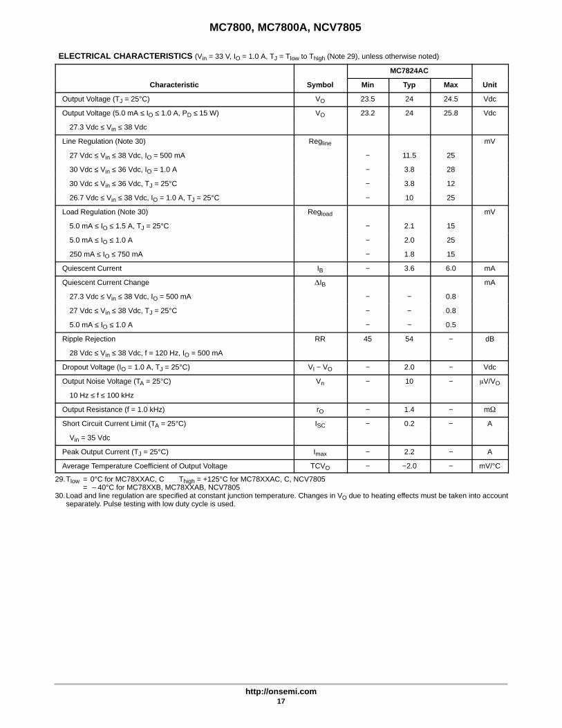
ELECTRICAL CHARACTERISTICS (Vin = 33 V, IO = 1.0 A, TJ = Tlow to Thigh (Note 29), unless otherwise noted)
MC7824AC
Characteristic Symbol Min Typ Max Unit
Output Voltage (TJ = 25°C) VO 23.5 24 24.5 Vdc
Output Voltage (5.0 mA ≤ IO ≤ 1.0 A, PD ≤ 15 W) VO 23.2 24 25.8 Vdc
27.3 Vdc ≤ Vin ≤ 38 Vdc
Line Regulation (Note 30) Regline mV
27 Vdc ≤ Vin ≤ 38 Vdc, IO = 500 mA − 11.5 25
30 Vdc ≤ Vin ≤ 36 Vdc, IO = 1.0 A − 3.8 28
30 Vdc ≤ Vin ≤ 36 Vdc, TJ = 25°C − 3.8 12
26.7 Vdc ≤ Vin ≤ 38 Vdc, IO = 1.0 A, TJ = 25°C − 10 25
Load Regulation (Note 30) Regload mV
5.0 mA ≤ IO ≤ 1.5 A, TJ = 25°C − 2.1 15
5.0 mA ≤ IO ≤ 1.0 A − 2.0 25
250 mA ≤ IO ≤ 750 mA − 1.8 15
Quiescent Current IB − 3.6 6.0 mA
Quiescent Current Change IB mA
27.3 Vdc ≤ Vin ≤ 38 Vdc, IO = 500 mA − − 0.8
27 Vdc ≤ Vin ≤ 38 Vdc, TJ = 25°C − − 0.8
5.0 mA ≤ IO ≤ 1.0 A − − 0.5
Ripple Rejection RR 45 54 − dB
28 Vdc ≤ Vin ≤ 38 Vdc, f = 120 Hz, IO = 500 mA
Dropout Voltage (IO = 1.0 A, TJ = 25°C) VI − VO − 2.0 − Vdc
Output Noise Voltage (TA = 25°C) Vn − 10 − V/VO
10 Hz ≤ f ≤ 100 kHz
Output Resistance (f = 1.0 kHz) rO − 1.4 − m
Short Circuit Current Limit (TA = 25°C) ISC − 0.2 − A
Vin = 35 Vdc
Peak Output Current (TJ = 25°C) Imax − 2.2 − A
Average Temperature Coefficient of Output Voltage TCVO − −2.0 − mV/°C
29.Tlow = 0°C for MC78XXAC, C Thigh = +125°C for MC78XXAC, C, NCV7805= 40°C for MC78XXB, MC78XXAB, NCV7805
30.Load and line regulation are specified at constant junction temperature. Changes in VO due to heating effects must be taken into accountseparately. Pulse testing with low duty cycle is used.

MC7800, MC7800A, NCV7805
http://onsemi.com18
Figure 2. Peak Output Current as a Function ofInput/Output Differential Voltage (MC78XXC, AC, B)
Figure 3. Ripple Rejection as a Function ofOutput Voltages (MC78XXC, AC, B)
Figure 4. Ripple Rejection as a Function ofFrequency (MC78XXC, AC, B)
Figure 5. Output Voltage as a Function ofJunction Temperature (MC7805C, AC, B)
Figure 6. Output Impedance as a Function ofOutput Voltage (MC78XXC, AC, B)
Figure 7. Quiescent Current as a Function ofTemperature (MC78XXC, AC, B)
I O
Vin−Vout, INPUT/OUTPUT VOLTAGE DIFFERENTIAL (V)
3.0
2.0
1.5
1.0
04.0 8.0 12 20 30 40
, OU
TP
UT
CU
RR
EN
T (A
)80
70
60
50
404.0 6.0 8.0 10 12 14 16 18 20 22 24
VO, OUTPUT VOLTAGE (V)
RR
, RIP
PLE
RE
JEC
TIO
N (
dB)
PART # VinMC7805C= 10 VMC7806C= 11 VMC7808C= 14 VMC7812C= 19 VMC7815C= 23 VMC7818C= 27 VMC7824C= 33 V
80
50
RR
, RIP
PLE
RE
JEC
TIO
N (
dB)
0.1 10
f, FREQUENCY (kHz)
0.01
, OU
TP
UT
VO
LTA
GE
(V
)O
5.0
4.9
−60 −20 20 60 100 140 180
TJ, JUNCTION TEMPERATURE (°C)
V
, OU
TP
UT
IMP
ED
AN
CE
(m
)
OΩ
10
5.0
3.0
2.0
1.0
0.5
0.3
0.2
0.14.0 8.0 12 16 20 24
VO, OUTPUT VOLTAGE (V)
Z
, QU
IES
CE
NT
CU
RR
EN
T (m
A)
B
6.0
4.0
3.0
2.0
1.0
0−75 −50
TJ, JUNCTION TEMPERATURE (°C)
−25 0 25 50 75 100 125
I
2.5
0.5
70
40
30
60
4.8
6.0 10 15 25 35
TJ = 85°C
TJ = 25°C
1.0
f = 120 HzIO = 20 mAVin = 1.0 V(RMS)
TJ = 125°C
TJ = 0°C
f = 120 HzIO = 500 mACL = 0 F
Vin = 10 VVO = 5.0 VIL = 20 mA
Vin = 20 VIO = 5.0 mA
MC78XXB, C, AC
Vin = 8.0 V to 18 VIO = 500 mAf = 120 HzTA = 25°C
TJ = −40°C
MC7800, MC7800A, NCV7805
http://onsemi.com19
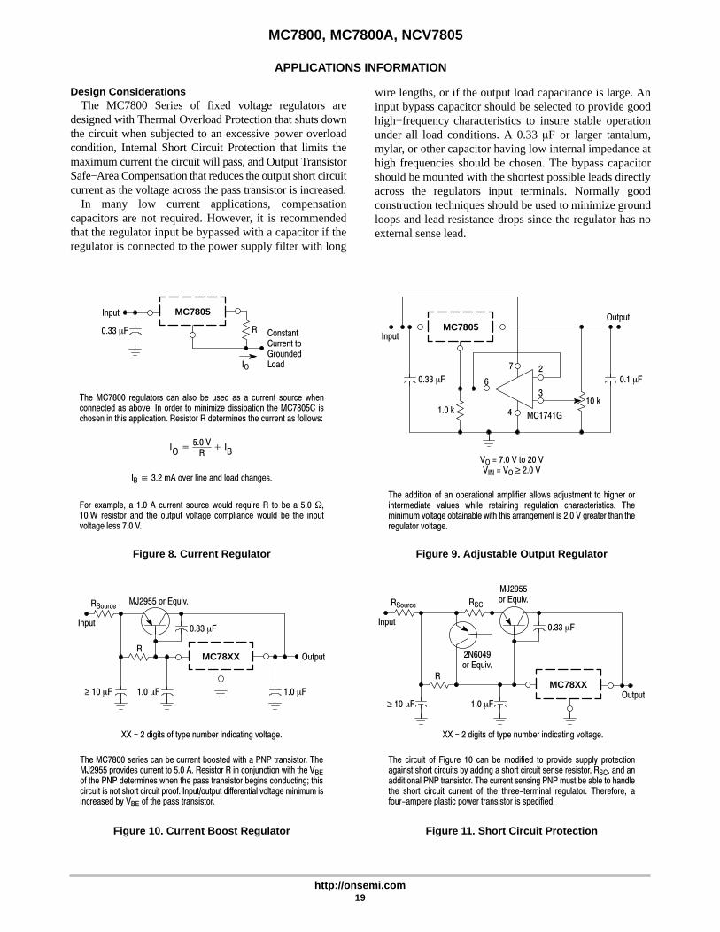
APPLICATIONS INFORMATION
Design ConsiderationsThe MC7800 Series of fixed voltage regulators are
designed with Thermal Overload Protection that shuts downthe circuit when subjected to an excessive power overloadcondition, Internal Short Circuit Protection that limits themaximum current the circuit will pass, and Output TransistorSafe−Area Compensation that reduces the output short circuitcurrent as the voltage across the pass transistor is increased.
In many low current applications, compensationcapacitors are not required. However, it is recommendedthat the regulator input be bypassed with a capacitor if theregulator is connected to the power supply filter with long
wire lengths, or if the output load capacitance is large. Aninput bypass capacitor should be selected to provide goodhigh−frequency characteristics to insure stable operationunder all load conditions. A 0.33 F or larger tantalum,mylar, or other capacitor having low internal impedance athigh frequencies should be chosen. The bypass capacitorshould be mounted with the shortest possible leads directlyacross the regulators input terminals. Normally goodconstruction techniques should be used to minimize groundloops and lead resistance drops since the regulator has noexternal sense lead.
IO 5.0V
R I
B
Figure 8. Current Regulator Figure 9. Adjustable Output Regulator
Figure 10. Current Boost Regulator Figure 11. Short Circuit Protection
The MC7800 regulators can also be used as a current source whenconnected as above. In order to minimize dissipation the MC7805C ischosen in this application. Resistor R determines the current as follows:
For example, a 1.0 A current source would require R to be a 5.0 ,10 W resistor and the output voltage compliance would be the inputvoltage less 7.0 V.
IB 3.2 mA over line and load changes.
Input
0.33 F R
IO
MC7805
ConstantCurrent toGroundedLoad
The addition of an operational amplifier allows adjustment to higher orintermediate values while retaining regulation characteristics. Theminimum voltage obtainable with this arrangement is 2.0 V greater than theregulator voltage.
InputMC7805
Output
0.33 F
10 k
MC1741G
7
6
41.0 k
VO = 7.0 V to 20 VVIN = VO ≥ 2.0 V
0.1 F
3
2
The MC7800 series can be current boosted with a PNP transistor. TheMJ2955 provides current to 5.0 A. Resistor R in conjunction with the VBEof the PNP determines when the pass transistor begins conducting; thiscircuit is not short circuit proof. Input/output differential voltage minimum isincreased by VBE of the pass transistor.
XX = 2 digits of type number indicating voltage.
MC78XX
Input
OutputR
1.0 F
MJ2955 or Equiv.
1.0 F
The circuit of Figure 10 can be modified to provide supply protectionagainst short circuits by adding a short circuit sense resistor, RSC, and anadditional PNP transistor. The current sensing PNP must be able to handlethe short circuit current of the three−terminal regulator. Therefore, afour−ampere plastic power transistor is specified.
XX = 2 digits of type number indicating voltage.
1.0 F
MC78XX
MJ2955or Equiv.
Output
RSC
R
2N6049or Equiv.
≥ 10 F
RSource
0.33 FInput
RSource
0.33 F
≥ 10 F
MC7800, MC7800A, NCV7805
http://onsemi.com20
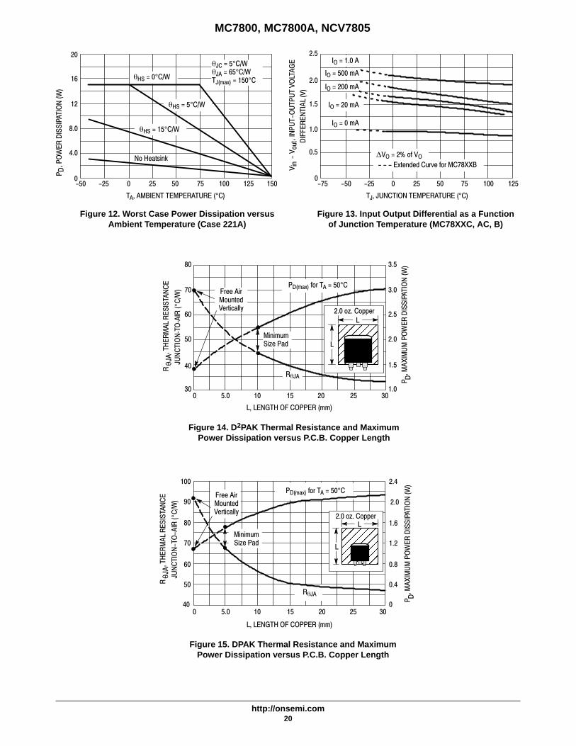
Figure 12. Worst Case Power Dissipation versusAmbient Temperature (Case 221A)
Figure 13. Input Output Differential as a Functionof Junction Temperature (MC78XXC, AC, B)
, PO
WE
R D
ISS
IPA
TIO
N (
W)
D20
16
12
8.0
4.0
0−50 −25 0 25 50 75 100 125 150
TA, AMBIENT TEMPERATURE (°C)
P
HS = 0°C/W
DIF
FE
RE
NT
IAL
(V)
inou
t, IN
PU
T−O
UT
PU
T V
OLT
AG
E
0.5
0−75 −50 −25 0 25 50 75 100 125
TJ, JUNCTION TEMPERATURE (°C)
− V
V
IO = 0 mA
IO = 20 mA
IO = 1.0 A
IO = 500 mA
IO = 200 mA
VO = 2% of VO
− − − Extended Curve for MC78XXB
JC = 5°C/WJA = 65°C/WTJ(max) = 150°C
HS = 5°C/W
HS = 15°C/W
No Heatsink
2.0
1.5
1.0
2.5
Figure 14. D 2PAK Thermal Resistance and MaximumPower Dissipation versus P.C.B. Copper Length
R, T
HE
RM
AL
RE
SIS
TAN
CE
JAθ JUN
CT
ION
-TO
-AIR
( C
/W)
°
30
40
50
60
70
80
1.0
1.5
2.0
2.5
3.0
3.5
0 10 20 3025155.0
L, LENGTH OF COPPER (mm)
PD(max) for TA = 50°C
MinimumSize Pad
2.0 oz. Copper
L
L
ÎÎÎÎÎÎÎÎÎÎÎÎÎÎÎÎ
Free AirMountedVertically
P D, M
AX
IMU
M P
OW
ER
DIS
SIP
AT
ION
(W
)
RJA
40
50
60
70
80
90
100
0
0.4
0.8
1.2
1.6
2.0
2.4
0 10 20 3025155.0
L, LENGTH OF COPPER (mm)
PD(max) for TA = 50°C
MinimumSize Pad
P D
L
L
ÎÎÎÎÎÎÎÎÎÎÎÎÎÎÎÎ
, MA
XIM
UM
PO
WE
R D
ISS
IPA
TIO
N (
W)
Free AirMountedVertically
RJA
2.0 oz. Copper
R, T
HE
RM
AL
RE
SIS
TAN
CE
JAθ JUN
CT
ION
−TO
−AIR
( C
/W)
°
Figure 15. DPAK Thermal Resistance and MaximumPower Dissipation versus P.C.B. Copper Length
MC7800, MC7800A, NCV7805
http://onsemi.com21
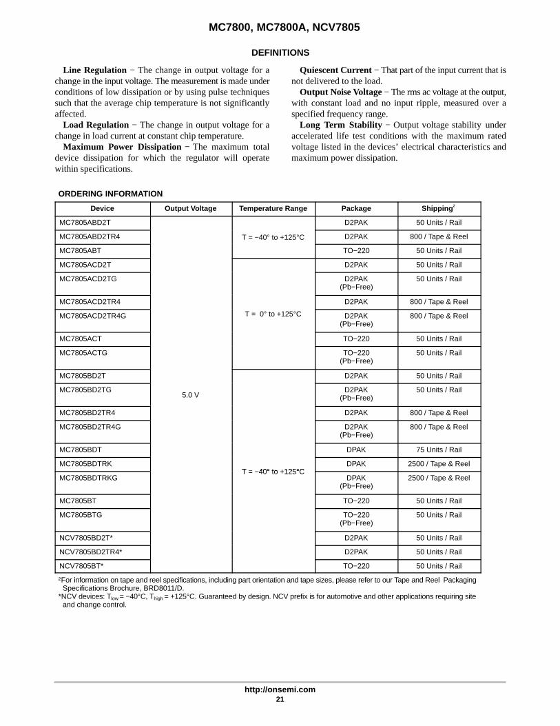
DEFINITIONS
Line Regulation − The change in output voltage for achange in the input voltage. The measurement is made underconditions of low dissipation or by using pulse techniquessuch that the average chip temperature is not significantlyaffected.
Load Regulation − The change in output voltage for achange in load current at constant chip temperature.
Maximum Power Dissipation − The maximum totaldevice dissipation for which the regulator will operatewithin specifications.
Quiescent Current − That part of the input current that isnot delivered to the load.
Output Noise Voltage − The rms ac voltage at the output,with constant load and no input ripple, measured over aspecified frequency range.
Long Term Stability − Output voltage stability underaccelerated life test conditions with the maximum ratedvoltage listed in the devices’ electrical characteristics andmaximum power dissipation.
ORDERING INFORMATION
Device Output Voltage Temperature Range Package Shipping †
MC7805ABD2T D2PAK 50 Units / Rail
MC7805ABD2TR4 T = −40° to +125°C D2PAK 800 / Tape & Reel
MC7805ABT TO−220 50 Units / Rail
MC7805ACD2T D2PAK 50 Units / Rail
MC7805ACD2TG D2PAK(Pb−Free)
50 Units / Rail
MC7805ACD2TR4 D2PAK 800 / Tape & Reel
MC7805ACD2TR4G T = 0° to +125°C D2PAK(Pb−Free)
800 / Tape & Reel
MC7805ACT TO−220 50 Units / Rail
MC7805ACTG TO−220(Pb−Free)
50 Units / Rail
MC7805BD2T D2PAK 50 Units / Rail
MC7805BD2TG5.0 V
D2PAK(Pb−Free)
50 Units / Rail
MC7805BD2TR4 D2PAK 800 / Tape & Reel
MC7805BD2TR4G D2PAK(Pb−Free)
800 / Tape & Reel
MC7805BDT DPAK 75 Units / Rail
MC7805BDTRKT 40° to +125°C
DPAK 2500 / Tape & Reel
MC7805BDTRKGT = −40° to +125°C
DPAK(Pb−Free)
2500 / Tape & Reel
MC7805BT TO−220 50 Units / Rail
MC7805BTG TO−220(Pb−Free)
50 Units / Rail
NCV7805BD2T* D2PAK 50 Units / Rail
NCV7805BD2TR4* D2PAK 50 Units / Rail
NCV7805BT* TO−220 50 Units / Rail
†For information on tape and reel specifications, including part orientation and tape sizes, please refer to our Tape and Reel PackagingSpecifications Brochure, BRD8011/D.
*NCV devices: Tlow = −40°C, Thigh = +125°C. Guaranteed by design. NCV prefix is for automotive and other applications requiring siteand change control.
MC7800, MC7800A, NCV7805
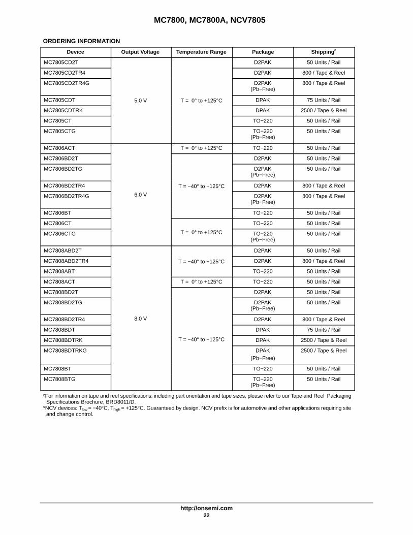
http://onsemi.com22
ORDERING INFORMATION
Device Shipping †PackageTemperature RangeOutput Voltage
MC7805CD2T D2PAK 50 Units / Rail
MC7805CD2TR4 D2PAK 800 / Tape & Reel
MC7805CD2TR4G D2PAK(Pb−Free)
800 / Tape & Reel
MC7805CDT 5.0 V T = 0° to +125°C DPAK 75 Units / Rail
MC7805CDTRK DPAK 2500 / Tape & Reel
MC7805CT TO−220 50 Units / Rail
MC7805CTG TO−220(Pb−Free)
50 Units / Rail
MC7806ACT T = 0° to +125°C TO−220 50 Units / Rail
MC7806BD2T D2PAK 50 Units / Rail
MC7806BD2TG D2PAK(Pb−Free)
50 Units / Rail
MC7806BD2TR4 T = −40° to +125°C D2PAK 800 / Tape & Reel
MC7806BD2TR4G 6.0 V D2PAK(Pb−Free)
800 / Tape & Reel
MC7806BT TO−220 50 Units / Rail
MC7806CT TO−220 50 Units / Rail
MC7806CTG T = 0° to +125°C TO−220(Pb−Free)
50 Units / Rail
MC7808ABD2T D2PAK 50 Units / Rail
MC7808ABD2TR4 T = −40° to +125°C D2PAK 800 / Tape & Reel
MC7808ABT TO−220 50 Units / Rail
MC7808ACT T = 0° to +125°C TO−220 50 Units / Rail
MC7808BD2T D2PAK 50 Units / Rail
MC7808BD2TG D2PAK(Pb−Free)
50 Units / Rail
MC7808BD2TR4 8.0 V D2PAK 800 / Tape & Reel
MC7808BDT DPAK 75 Units / Rail
MC7808BDTRK T = −40° to +125°C DPAK 2500 / Tape & Reel
MC7808BDTRKG DPAK(Pb−Free)
2500 / Tape & Reel
MC7808BT TO−220 50 Units / Rail
MC7808BTG TO−220(Pb−Free)
50 Units / Rail
†For information on tape and reel specifications, including part orientation and tape sizes, please refer to our Tape and Reel PackagingSpecifications Brochure, BRD8011/D.
*NCV devices: Tlow = −40°C, Thigh = +125°C. Guaranteed by design. NCV prefix is for automotive and other applications requiring siteand change control.
MC7800, MC7800A, NCV7805
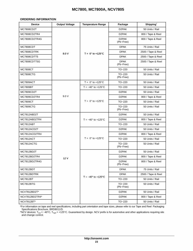
http://onsemi.com23
ORDERING INFORMATION
Device Shipping †PackageTemperature RangeOutput Voltage
MC7808CD2T D2PAK 50 Units / Rail
MC7808CD2TR4 D2PAK 800 / Tape & Reel
MC7808CD2TR4G D2PAK(Pb−Free)
800 / Tape & Reel
MC7808CDT DPAK 75 Units / Rail
MC7808CDTRK8.0 V T = 0° to +125°C
DPAK 2500 / Tape & Reel
MC7808CDTT58.0 V T = 0° to +125°C
DPAK 2500 / Tape & Reel
MC7808CDTT5G DPAK(Pb−Free)
2500 / Tape & Reel
MC7808CT TO−220 50 Units / Rail
MC7808CTG TO−220(Pb−Free)
50 Units / Rail
MC7809ACT T = 0° to +125°C TO−220 50 Units / Rail
MC7809BT T = −40° to +125°C TO−220 50 Units / Rail
MC7809CD2T D2PAK 50 Units / Rail
MC7809CD2TR4 9.0 V D2PAK 800 / Tape & Reel
MC7809CT T = 0° to +125°C TO−220 50 Units / Rail
MC7809CTG TO−220(Pb−Free)
50 Units / Rail
MC7812ABD2T D2PAK 50 Units / Rail
MC7812ABD2TR4 T = −40° to +125°C D2PAK 800 / Tape & Reel
MC7812ABT TO−220 50 Units / Rail
MC7812ACD2T D2PAK 50 Units / Rail
MC7812ACD2TR4 D2PAK 800 / Tape & Reel
MC7812ACT T = 0° to +125°C TO−220 50 Units / Rail
MC7812ACTG TO−220(Pb−Free)
50 Units / Rail
MC7812BD2T D2PAK 50 Units / Rail
MC7812BD2TR412 V
D2PAK 800 / Tape & Reel
MC7812BD2TR4G12 V
D2PAK(Pb−Free)
800 / Tape & Reel
MC7812BDT DPAK 75 Units / Rail
MC7812BDTRKT 40° to +125°C
DPAK 2500 / Tape & Reel
MC7812BTT = −40° to +125°C
TO−220 50 Units / Rail
MC7812BTG TO−220(Pb−Free)
50 Units / Rail
NCV7812BD2T* D2PAK 50 Units / Rail
NCV7812BD2TR4* D2PAK 800 / Tape & Reel
NCV7812BT* TO−220 50 Units / Rail
†For information on tape and reel specifications, including part orientation and tape sizes, please refer to our Tape and Reel PackagingSpecifications Brochure, BRD8011/D.
*NCV devices: Tlow = −40°C, Thigh = +125°C. Guaranteed by design. NCV prefix is for automotive and other applications requiring siteand change control.
MC7800, MC7800A, NCV7805
http://onsemi.com24
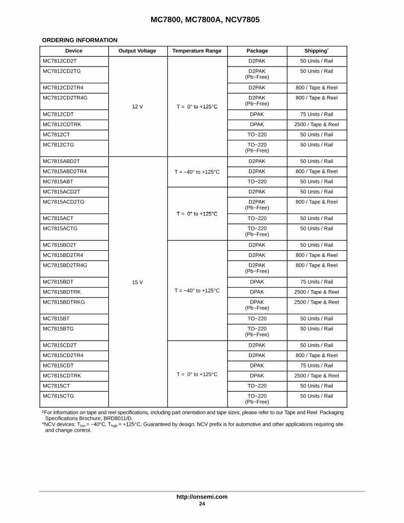
ORDERING INFORMATION
Device Shipping †PackageTemperature RangeOutput Voltage
MC7812CD2T D2PAK 50 Units / Rail
MC7812CD2TG D2PAK(Pb−Free)
50 Units / Rail
MC7812CD2TR4 D2PAK 800 / Tape & Reel
MC7812CD2TR4G
12 V T = 0° to +125°C
D2PAK(Pb−Free)
800 / Tape & Reel
MC7812CDT
12 V T = 0 to +125 C
DPAK 75 Units / Rail
MC7812CDTRK DPAK 2500 / Tape & Reel
MC7812CT TO−220 50 Units / Rail
MC7812CTG TO−220(Pb−Free)
50 Units / Rail
MC7815ABD2T D2PAK 50 Units / Rail
MC7815ABD2TR4 T = −40° to +125°C D2PAK 800 / Tape & Reel
MC7815ABT TO−220 50 Units / Rail
MC7815ACD2T D2PAK 50 Units / Rail
MC7815ACD2TG
T 0° to +125°C
D2PAK(Pb−Free)
800 / Tape & Reel
MC7815ACTT = 0° to +125°C
TO−220 50 Units / Rail
MC7815ACTG TO−220(Pb−Free)
50 Units / Rail
MC7815BD2T D2PAK 50 Units / Rail
MC7815BD2TR4 D2PAK 800 / Tape & Reel
MC7815BD2TR4G D2PAK(Pb−Free)
800 / Tape & Reel
MC7815BDT 15 V DPAK 75 Units / Rail
MC7815BDTRK T = −40° to +125°C DPAK 2500 / Tape & Reel
MC7815BDTRKG DPAK(Pb−Free)
2500 / Tape & Reel
MC7815BT TO−220 50 Units / Rail
MC7815BTG TO−220(Pb−Free)
50 Units / Rail
MC7815CD2T D2PAK 50 Units / Rail
MC7815CD2TR4 D2PAK 800 / Tape & Reel
MC7815CDT DPAK 75 Units / Rail
MC7815CDTRK T = 0° to +125°C DPAK 2500 / Tape & Reel
MC7815CT TO−220 50 Units / Rail
MC7815CTG TO−220(Pb−Free)
50 Units / Rail
†For information on tape and reel specifications, including part orientation and tape sizes, please refer to our Tape and Reel PackagingSpecifications Brochure, BRD8011/D.
*NCV devices: Tlow = −40°C, Thigh = +125°C. Guaranteed by design. NCV prefix is for automotive and other applications requiring siteand change control.
MC7800, MC7800A, NCV7805
http://onsemi.com25
ORDERING INFORMATION
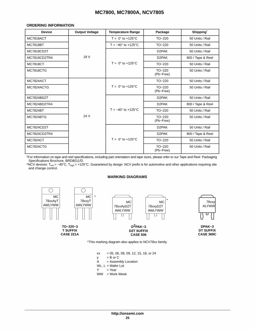
Device Shipping †PackageTemperature RangeOutput Voltage
MC7818ACT T = 0° to +125°C TO−220 50 Units / Rail
MC7818BT T = −40° to +125°C TO−220 50 Units / Rail
MC7818CD2T D2PAK 50 Units / Rail
MC7818CD2TR4 18 V D2PAK 800 / Tape & Reel
MC7818CT T = 0° to +125°C TO−220 50 Units / Rail
MC7818CTG TO−220(Pb−Free)
50 Units / Rail
MC7824ACT TO−220 50 Units / Rail
MC7824ACTG T = 0° to +125°C TO−220(Pb−Free)
50 Units / Rail
MC7824BD2T D2PAK 50 Units / Rail
MC7824BD2TR4 D2PAK 800 / Tape & Reel
MC7824BT T = −40° to +125°C TO−220 50 Units / Rail
MC7824BTG 24 V TO−220(Pb−Free)
50 Units / Rail
MC7824CD2T D2PAK 50 Units / Rail
MC7824CD2TR4 D2PAK 800 / Tape & Reel
MC7824CT T = 0° to +125°C TO−220 50 Units / Rail
MC7824CTG TO−220(Pb−Free)
50 Units / Rail
†For information on tape and reel specifications, including part orientation and tape sizes, please refer to our Tape and Reel PackagingSpecifications Brochure, BRD8011/D.
*NCV devices: Tlow = −40°C, Thigh = +125°C. Guaranteed by design. NCV prefix is for automotive and other applications requiring siteand change control.
78xxAyD2TAWLYWW
MC78xxAyT
AWLYWW
xx = 05, 06, 08, 09, 12, 15, 18, or 24y = B or CA = Assembly LocationWL, L = Wafer LotY = YearWW = Work Week
MARKING DIAGRAMS
TO−220−3T SUFFIX
CASE 221A
MC
D2PAK−3D2T SUFFIXCASE 936
DPAK−3DT SUFFIXCASE 369C
78xxyALYWW78xxyD2T
AWLYWW
MC*
MC78xxyT
AWLYWW
*
*This marking diagram also applies to NCV78xx family.
MC7800, MC7800A, NCV7805
http://onsemi.com26
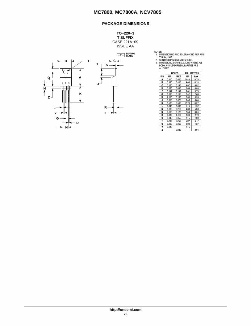
PACKAGE DIMENSIONS
TO−220−3T SUFFIX
CASE 221A−09ISSUE AA
NOTES:1. DIMENSIONING AND TOLERANCING PER ANSI
Y14.5M, 1982.2. CONTROLLING DIMENSION: INCH.3. DIMENSION Z DEFINES A ZONE WHERE ALL
BODY AND LEAD IRREGULARITIES AREALLOWED.
DIM MIN MAX MIN MAX
MILLIMETERSINCHES
A 0.570 0.620 14.48 15.75
B 0.380 0.405 9.66 10.28
C 0.160 0.190 4.07 4.82
D 0.025 0.035 0.64 0.88
F 0.142 0.147 3.61 3.73
G 0.095 0.105 2.42 2.66
H 0.110 0.155 2.80 3.93
J 0.018 0.025 0.46 0.64
K 0.500 0.562 12.70 14.27
L 0.045 0.060 1.15 1.52
N 0.190 0.210 4.83 5.33
Q 0.100 0.120 2.54 3.04
R 0.080 0.110 2.04 2.79
S 0.045 0.055 1.15 1.39
T 0.235 0.255 5.97 6.47
U 0.000 0.050 0.00 1.27
V 0.045 −−− 1.15 −−−
Z −−− 0.080 −−− 2.04
B
Q
H
Z
L
V
G
N
A
K
F
1 2 3
4
D
SEATINGPLANE−T−
CST
U
R
J
MC7800, MC7800A, NCV7805
http://onsemi.com27
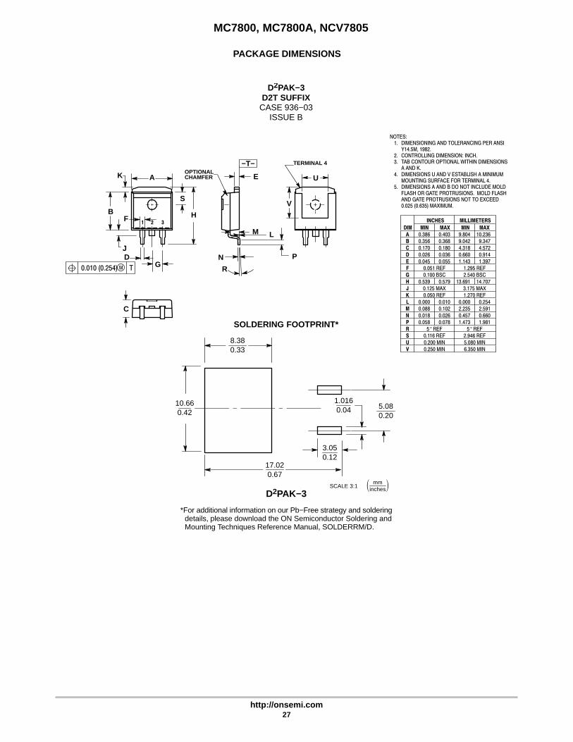
PACKAGE DIMENSIONS
D2PAK−3D2T SUFFIX
CASE 936−03ISSUE B
5 REF5 REF
V
U
TERMINAL 4
NOTES:1. DIMENSIONING AND TOLERANCING PER ANSI
Y14.5M, 1982.2. CONTROLLING DIMENSION: INCH.3. TAB CONTOUR OPTIONAL WITHIN DIMENSIONS
A AND K.4. DIMENSIONS U AND V ESTABLISH A MINIMUM
MOUNTING SURFACE FOR TERMINAL 4.5. DIMENSIONS A AND B DO NOT INCLUDE MOLD
FLASH OR GATE PROTRUSIONS. MOLD FLASHAND GATE PROTRUSIONS NOT TO EXCEED0.025 (0.635) MAXIMUM.
DIM
A
MIN MAX MIN MAX
MILLIMETERS
0.386 0.403 9.804 10.236
INCHES
B 0.356 0.368 9.042 9.347
C 0.170 0.180 4.318 4.572
D 0.026 0.036 0.660 0.914
E 0.045 0.055 1.143 1.397
F 0.051 REF 1.295 REF
G 0.100 BSC 2.540 BSC
H 0.539 0.579 13.691 14.707
J 0.125 MAX 3.175 MAX
K 0.050 REF 1.270 REF
L 0.000 0.010 0.000 0.254
M 0.088 0.102 2.235 2.591
N 0.018 0.026 0.457 0.660
P 0.058 0.078 1.473 1.981
R
S 0.116 REF 2.946 REF
U 0.200 MIN 5.080 MIN
V 0.250 MIN 6.350 MIN
A
1 2 3
K
FB
J
S
H
DG
C
M0.010 (0.254) T
E
M L
PN
R
−T−OPTIONALCHAMFER
D2PAK−3
*For additional information on our Pb−Free strategy and solderingdetails, please download the ON Semiconductor Soldering andMounting Techniques Reference Manual, SOLDERRM/D.
SOLDERING FOOTPRINT*
8.380.33
1.0160.04
17.020.67
10.660.42
3.050.12
5.080.20
mminches
SCALE 3:1
MC7800, MC7800A, NCV7805
http://onsemi.com28
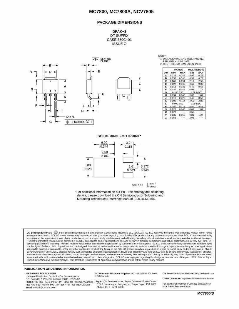
PACKAGE DIMENSIONS
DPAK−3DT SUFFIX
CASE 369C−01ISSUE O
D
A
K
B
RV
S
FL
G
2 PL
M0.13 (0.005) T
E
C
U
J
H
−T− SEATINGPLANE
Z
DIM MIN MAX MIN MAXMILLIMETERSINCHES
A 0.235 0.245 5.97 6.22B 0.250 0.265 6.35 6.73C 0.086 0.094 2.19 2.38D 0.027 0.035 0.69 0.88E 0.018 0.023 0.46 0.58F 0.037 0.045 0.94 1.14G 0.180 BSC 4.58 BSCH 0.034 0.040 0.87 1.01J 0.018 0.023 0.46 0.58K 0.102 0.114 2.60 2.89L 0.090 BSC 2.29 BSCR 0.180 0.215 4.57 5.45S 0.025 0.040 0.63 1.01U 0.020 −−− 0.51 −−−V 0.035 0.050 0.89 1.27Z 0.155 −−− 3.93 −−−
NOTES:1. DIMENSIONING AND TOLERANCING
PER ANSI Y14.5M, 1982.2. CONTROLLING DIMENSION: INCH.
1 2 3
4
5.800.228
2.580.101
1.60.063
6.200.244
3.00.118
6.1720.243
mminches
SCALE 3:1
*For additional information on our Pb−Free strategy and solderingdetails, please download the ON Semiconductor Soldering andMounting Techniques Reference Manual, SOLDERRM/D.
SOLDERING FOOTPRINT*
ON Semiconductor and are registered trademarks of Semiconductor Components Industries, LLC (SCILLC). SCILLC reserves the right to make changes without further noticeto any products herein. SCILLC makes no warranty, representation or guarantee regarding the suitability of its products for any particular purpose, nor does SCILLC assume any liabilityarising out of the application or use of any product or circuit, and specifically disclaims any and all liability, including without limitation special, consequential or incidental damages.“Typical” parameters which may be provided in SCILLC data sheets and/or specifications can and do vary in different applications and actual performance may vary over time. Alloperating parameters, including “Typicals” must be validated for each customer application by customer’s technical experts. SCILLC does not convey any license under its patent rightsnor the rights of others. SCILLC products are not designed, intended, or authorized for use as components in systems intended for surgical implant into the body, or other applicationsintended to support or sustain life, or for any other application in which the failure of the SCILLC product could create a situation where personal injury or death may occur. ShouldBuyer purchase or use SCILLC products for any such unintended or unauthorized application, Buyer shall indemnify and hold SCILLC and its officers, employees, subsidiaries, affiliates,and distributors harmless against all claims, costs, damages, and expenses, and reasonable attorney fees arising out of, directly or indirectly, any claim of personal injury or deathassociated with such unintended or unauthorized use, even if such claim alleges that SCILLC was negligent regarding the design or manufacture of the part. SCILLC is an EqualOpportunity/Affirmative Action Employer. This literature is subject to all applicable copyright laws and is not for resale in any manner.
PUBLICATION ORDERING INFORMATIONN. American Technical Support : 800−282−9855 Toll FreeUSA/Canada
Japan : ON Semiconductor, Japan Customer Focus Center2−9−1 Kamimeguro, Meguro−ku, Tokyo, Japan 153−0051Phone : 81−3−5773−3850
MC7800/D
LITERATURE FULFILLMENT :Literature Distribution Center for ON SemiconductorP.O. Box 61312, Phoenix, Arizona 85082−1312 USAPhone : 480−829−7710 or 800−344−3860 Toll Free USA/CanadaFax: 480−829−7709 or 800−344−3867 Toll Free USA/CanadaEmail : [email protected]
ON Semiconductor Website : http://onsemi.com
Order Literature : http://www.onsemi.com/litorder
For additional information, please contact yourlocal Sales Representative.

This datasheet has been download from:
www.datasheetcatalog.com
Datasheets for electronics components.