
On Optimum Design of Planar Microwave Components under ...
10
On Optimum Design of Planar Microwave Components under Linearity Constraints Shitvov, A., Kozlov, D., & Schuchinsky, A. (2017). On Optimum Design of Planar Microwave Components under Linearity Constraints. In Proceedings of the 9th International Workshop on Multipactor, Corona and Passive Intermodulation 2017 Published in: Proceedings of the 9th International Workshop on Multipactor, Corona and Passive Intermodulation 2017 Document Version: Peer reviewed version Queen's University Belfast - Research Portal: Link to publication record in Queen's University Belfast Research Portal Publisher rights © 2017 Val Space Consortium. This work is made available online in accordance with the publisher’s policies. Please refer to any applicable terms of use of the publisher. General rights Copyright for the publications made accessible via the Queen's University Belfast Research Portal is retained by the author(s) and / or other copyright owners and it is a condition of accessing these publications that users recognise and abide by the legal requirements associated with these rights. Take down policy The Research Portal is Queen's institutional repository that provides access to Queen's research output. Every effort has been made to ensure that content in the Research Portal does not infringe any person's rights, or applicable UK laws. If you discover content in the Research Portal that you believe breaches copyright or violates any law, please contact [email protected]. Download date:09. Feb. 2022
Transcript of On Optimum Design of Planar Microwave Components under ...

On Optimum Design of Planar Microwave Components underLinearity Constraints
Shitvov, A., Kozlov, D., & Schuchinsky, A. (2017). On Optimum Design of Planar Microwave Components underLinearity Constraints. In Proceedings of the 9th International Workshop on Multipactor, Corona and PassiveIntermodulation 2017
Published in:Proceedings of the 9th International Workshop on Multipactor, Corona and Passive Intermodulation 2017
Document Version:Peer reviewed version
Queen's University Belfast - Research Portal:Link to publication record in Queen's University Belfast Research Portal
Publisher rights© 2017 Val Space Consortium.This work is made available online in accordance with the publisher’s policies. Please refer to any applicable terms of use of the publisher.
General rightsCopyright for the publications made accessible via the Queen's University Belfast Research Portal is retained by the author(s) and / or othercopyright owners and it is a condition of accessing these publications that users recognise and abide by the legal requirements associatedwith these rights.
Take down policyThe Research Portal is Queen's institutional repository that provides access to Queen's research output. Every effort has been made toensure that content in the Research Portal does not infringe any person's rights, or applicable UK laws. If you discover content in theResearch Portal that you believe breaches copyright or violates any law, please contact [email protected].
Download date:09. Feb. 2022

On Optimum Design of Planar Microwave Components underLinearity Constraints
Shitvov, A., Kozlov, D., & Schuchinsky, A. (2017). On Optimum Design of Planar Microwave Components underLinearity Constraints. 1. Paper presented at 9th International Workshop on Multipactor, Corona and PassiveIntermodulation 2017, Noordwijk, Netherlands.
Document Version:Peer reviewed version
Queen's University Belfast - Research Portal:Link to publication record in Queen's University Belfast Research Portal
General rightsCopyright for the publications made accessible via the Queen's University Belfast Research Portal is retained by the author(s) and / or othercopyright owners and it is a condition of accessing these publications that users recognise and abide by the legal requirements associatedwith these rights.
Take down policyThe Research Portal is Queen's institutional repository that provides access to Queen's research output. Every effort has been made toensure that content in the Research Portal does not infringe any person's rights, or applicable UK laws. If you discover content in theResearch Portal that you believe breaches copyright or violates any law, please contact [email protected].
Download date:26. Apr. 2017

On Optimum Design of Planar Microwave Components under Linearity Constraints
Alexey Shitvov(1), Dmitry Kozlov(1), Alexander Schuchinsky(2)
(1)The Institute of Electronics, Communications and Information Theory (ECIT), Queen’s University Belfast
Queen’s Road, Belfast, BT3 9DT, United Kingdom
Email: [email protected]
(2)Department of Electrical Engineering & Electronics of the University of Liverpool
Email: [email protected]
INTRODUCTION
Basic signal impairments in printed circuits arising from the intrinsic electrical nonlinearities of strip conductors and
substrate materials have been duly recognised and studied since 1990-s, particularly in application to superconducting
microstrip lines (SCML) [1-3] and tuneable microstrip lines on ferroelectric [4-5] and liquid crystal substrates [6]. The
reported simulation and experimental studies of the third-order intermodulation (IM3) in SCML resonators and filters
[3, 7-9] revealed some characteristic features of nonlinear products which suggested mitigation of the nonlinear
response by optimising the filter topology. In particular, in [3] using a simple second-order polynomial model of
nonlinear p.u.l. inductance, it was shown by simulations that the output IM3 product generated in a microstrip resonator
is proportional to the power four of the resonator loaded quality factor and inversely proportional to the resonator length
squared and microstrip width squared. The output IM response of a filter comprising several coupled resonators with
varied loaded Q, resonance frequency and position along the main transmission line was calculated using a simple
circuit model to reveal the peaking IM level at the bandpass edges and individual contributions of the constituent
resonators. The sharp band edges proved to be associated with a higher IM peaking, which is also consistent with the
analysis in [7]. As the result, it was suggested that the IM generation due to the intrinsic superconductor nonlinearity
can be reduced by increasing the width of the transmission line (TL) sections, thus decreasing the current density at the
strip edges, as well as by finding optimum individual resonator Q-factors, resonance frequencies and locations with the
aid of the simulated annealing technique. Interestingly, it appeared that high-order resonator filters allow greater
improvement of the output linearity. It was also observed that directly reducing the peak current density in the selected
resonators that contribute stronger to the total IM response does not necessarily result in the minimum IM [3], which
warrants the need of a holistic approach to the filter design. Alternative approach is based on the microstrip resonator
topologies and modes that do not have associated peak currents, such as the TM010 mode of a disc resonator in [10].
The important aspect of the previous studies, particularly those concerned with the SCML microwave resonators and
filters, is the use of specific models of the intrinsic nonlinearity, albeit phenomenological and subject to experimental
characterisation, which nevertheless refer to the pre-determined physical mechanisms, i.e., deterministic dependences of
the superfluid density on the electric current density [11-12]. However, when it comes to the characterisation of the
intrinsic nonlinearities in ordinary planar circuits, fabricated on commercial RF laminate materials and operated at
ambient temperatures, exact mechanisms and location of nonlinearities are usually unknown a priori, so that the net
nonlinear response is rendered by multiple concurrent sources that may change in time being influenced by many
unpredictable factors. The great diversity and variability of the TL nonlinearities, including both distributed and lumped
(contact) sources, requires a different approach to characterisation, modelling and mitigation of the passive
intermodulation (PIM) generation in planar microwave circuits, resonators and filters.
In this paper, we adopt an efficient approach to accurate characterisation of the sources and mechanisms of intrinsic
nonlinearities in microstrip lines based upon the conventional two-tone PIM measurements. A simple physical model of
distributed PIM generation in uniform microstrip lines is presented, as well as the model of discontinuities. A numerical
implementation of the developed model using commercial RF CAD software is proposed and a simple microstrip filter
is designed and simulated. It is shown that the filter topology can be optimised to decrease both input and output PIM
response without sacrificing the linear performance. The results of our study suggest the need of further development of
efficient CAD tools for the design of complex planar microwave circuits under the linearity constraints.
MECHANISMS AND SOURCES OF INTRINSIC NONLINEARITIES IN MICROSTRIP LINES
Previous experimental studies of PCB materials for base-station antenna applications suggest strong correlation between
the PIM products in printed lines and characteristics of the constituent materials. In particular, stronger PIM generation
was observed on PCB laminates with higher conductor roughness profile, [13]. In further experimental studies, it was
also observed that significantly higher PIM can be generated due to the substrate nonlinearity, [14], but again no
specific sources of the nonlinear behavior have been identified. Some studies performed on the base-station grade PCB
materials and circuits consistently revealed strong effect of the PCB plating on the resulting PIM generation, as well as
the peculiar effects of the PCB etching, [15]. It should be noted that in almost all systematic studies of PIM generation
in commercial grade PCB materials the experimental methodology was usually based on the basic two-tone PIM tests
complemented by carrier power and/or frequency sweeps, and the PIM products were measured at the input or output
terminals of the tested specimens. However, such PIM characterisation does not provide sufficient details required for
understanding the physics of PCB nonlinearities and devising rigorous engineering approaches to PIM mitigation.
The advanced experimental methodologies, specifically those based on the near-field PIM probing [16] and broadband
intermodulation measurements with closely spaced carriers [17], allowed further insights in the mechanisms of PIM
generation in printed circuits. Specifically, the distributed nature of the PCB nonlinearity, omni-directional emission by
a lumped PIM source and the effects of the phase synchronism on distributed PIM generation have been confirmed
experimentally. It also revealed that diverse circuit parameters and intrinsic dynamics can contribute to nonlinear
distortions as well, e.g., ohmic heating in microstrip circuits with temperature-dependent resistivity [17]. Despite the
progress made in understanding the mechanisms of microstrip nonlinearities, the nonlinear models used are still based
upon basic static polynomials, whereas the model development and assessment have been largely overlooked. Recent
theoretical studies of nonlinearities represented by an equivalent memristor and non-analytical characteristics [18],
suggest that accurate model retrieval generally require simultaneous measurement of a wide range of intermodulation
products, which is incompatible with the specification of the available commercial and laboratory PIM analyzers.
Our recent experimental investigations of PIM generation in printed circuits fabricated on base-station antenna grade
PCB laminates suggest that certain microstrip nonlinearities often result from the PCB processing. For the present
study, we have selected the microstrip lines of different strip width, Fig. 1(a), exhibiting discernible “black tin”
contamination along the strip edges, as detailed in [19]. The used PTFE-based laminate with a low profile 1 oz. copper
cladding is qualified as a low-PIM material. The conductor pattern was finished with 1 um immersion-tin plating. The
PIM signal at frequency fIM3 = 2f1 – f2 = 910 MHz, where the carrier frequencies are f1 = 935 MHz and f2 = 960 MHz,
appeared to be more than 30 dB higher than the level measured on the same layout and material processed by the same
PCB workshop, but without visible contamination at the strip edges. The measured characteristic decrease of the PIM
level versus the microstrip width indicated conductor-type nonlinearity, so that the lower current density on wider strips
results in respectively lower PIM level. The effect of the return current on the ground-plane is much weaker due to the
lower current density. The near-field mapping of the PIM product distributions along and across signal strip suggests
that from the perspective of PIM modelling in our study, it is reasonable to assume a continuous distribution of the
conductor nonlinearity over the signal strip surface, thus ignoring the actual discreteness of the “black tin” PIM sources
at strip edges.
DISTRIBUTED MODEL OF PIM GENERATION IN MICROSTRIP LINES
From the viewpoint of the PIM characterisation in microstrip lines two main approaches can be adopted. The
behavioural modelling can be employed for nonlinear characterisation, where a section of microstrip circuit is
represented as a “black box” described by a global polynomial model providing the circuit output signal as the function
of the circuit input signal, [20]. For example, to analyse PIM performance of a planar microwave filter, it can be
represented by interconnection of TL sections and canonical discontinuities. So, once each constituent element has a
measured behavioural model, the filter response can be calculated with the aid of commercial RF CAD capable of
cascading multiple nonlinear components. Such an approach is not always convenient, since it requires repeated
measurements of the microstrip circuits if some of the parameters changes, e.g., microstrip line length or width, or even
the power of the input signal.
A more rigorous approach is based on equivalent circuits, where the circuit behaviour is represented by equivalent
components characterised by explicit dependence on the microstrip geometry and materials, [21]. In particular, the
nonlinear transmission line models have been extensively used for the analysis and modelling of distributed PIM
generation in printed transmission lines and the equivalent lumped element circuits and applied to the analysis of
nonlinear effects in microstrip resonators and filters [3, 9]. Utility of the latter approach, especially when the location of
nonlinear sources is concerned, is determined by a choice of the method for nonlinear characterisation.

As discussed above, we can assume that the microscopic PIM sources are evenly distributed and current-dependent.
They can be described by the equivalent circuit of the TL unit cell with the current-dependent p.u.l. resistance and/or
current-dependent p.u.l. inductance. It has been shown elsewhere that the effects of the resistive and reactive
nonlinearities on transmission lines can be discriminated by means of broadband measurements, i.e., can be deduced
from the concurrent measurements of the third-order intermodulation and third harmonic responses. However,
commercial PIM analysers available for our study did not support such a broad frequency range. Fortunately, the effects
of nonlinear kinetic inductance, [22], is negligible in conventional printed lines so that nonlinear current-dependent
resistance is the principal source of distributed PIM generation in printed circuits.
At the next step of the analysis, it is necessary to define a model of resistive nonlinearity. In most practical cases of
weakly nonlinear dependence of the TL parameters on the electric current, I, is described by a static polynomial with
only one current-dependent term. In principle other models are possible, e.g., to account for the limiter and memory
effects. The frequency-sweep measurements of the PIM products of different orders on the microstrip lines tested in our
study showed constant PIM level across the whole measured band when either of the carrier frequencies sweeps across
the Tx band. The PIM level also remained frequency invariant at different carrier powers. These observations suggest
negligible memory effects and circuit dynamics, so the resistive nonlinearity can be approximated by the polynomial:
1 22 4 2
0 0 2 4 0 21( ) ( ) ,
N n
NL nnR I R R I R R I R I R R I (1)
where N is odd and the coefficients R'2n are retrieved from experimental data. It is noteworthy that the nonlinear
resistance R'NL(I) of the TL unit cell is described by the polynomial of I2. Validity of such an approximation has been
verified by cross-band PIM measurements, where the sum product of the carrier frequencies from the E-GSM 900 band
was measured in the PCS 1900 band. The measured level of the second-order PIM products was below the noise floor
that corroborates the assumption used in the model (1) that no even-order PIM products are permitted.
Given the nonlinear transmission line model with the resistive nonlinearity (1) is supported by the experimental
observations, the complete mathematical description of the nonlinear voltage and current waveforms on a uniform
microstrip transmission line is given by the generalised telegrapher’s equations:
0 0
0 0
( , ) ( , )( , )
( , ) ( , )( , ) ( , )
NL
I x t V x tC G V x t
x t
V x t I x tL R I x t R I I x t
x t
(2)
The linear p.u.l. parameters R0', L0', C0' and G0' can be calculated by a quasi-static analysis and directly related to the
microstrip geometry. Using the Fourier series expansion under the assumption of weak nonlinearity, the nonlinear
system (2) can be solved for each intermodulation frequency 1 21 1 2M M M , as further detailed in
[21]. The resulting analytical approximations for the power of M-th order forward and reverse PIM products at the
output and input terminals of a matched uniform TL of length L, respectively, have the form:
22 2 2 2
22 2 2 2
0.5Re 1 ,
0.5Re 1 sin ,
M M
M M
L
fwd c M
rev c M M M
P L Z A M L e
P L Z A M L
(3)
where
1
2 22
2 2 21 0
ˆ 2 12 1ˆ ,
1 0.5 11 2
N
lM l
M ll M M
ll RIA I
l Ml Z
k
l
are the binomial coefficients, I is the current
amplitude assumed the same for both carriers at a carrier frequency, 0 0 0 0M M M MR j L G j C j ,
and 1 20.5 1 1 M M j M M . Closed-form expressions (3) show that the forward PIM increases
monotonically with the line length at L << 1. Conversely, the reverse PIM shows regular undulations as the line length
increases. Equations (3) can be directly used to characterise the TL nonlinearity defined by (1). Specifically, forward or
reverse PIM power at the corresponding terminal of a matched uniform TL can be measured in a range of carrier power
magnitudes and then the model of the nonlinear p.u.l. resistance (1) with N specified can be retrieved by fitting the

analytical curves (3) to the experimental results. Alternatively, near-field PIM probing can also be used for the model
retrieval, but in slightly different analytical form.
The closed-form equations (3) implicitly incorporate the PIM dependence on the strip width through the parameters of
the nonlinear model (1). The width-dependent nonlinear parameters can be derived by the quasi-static analysis. In
particular, considering the phenomenological volume resistivity ρ(J) = ρ0 + ρ2J2 +..., where J represents the non-uniform
current density, the corresponding coefficients of the nonlinear p.u.l. resistance are given by, cf. [12]:
/2
2 1 2 2 2 2
2 2/2
,
Wn n n
n n s sW
R I J dy (4)
where Js(y) is the surface current distribution across the thin signal strip of width W and δs is the skin depth. In
particular, in parallel-plate approximation, i.e., at low frequency, equation (4) reduces to 2 1 2 1
2 2
n n
n n sR W ,
which contributes to the dependence of PIM on the strip width, along with the Wheeler’s characteristic impedance and
other width-dependent parameters in (3).
The frequency dependence of the PIM products is also implied in the closed-form expressions (3) through the skin
depth and microstrip characteristic impedance. At high frequency the ordinary p.u.l. resistance is asymptotically
proportional to f , whereas the p.u.l. inductance depends on 1 f , [23]. Experimental data often show the PIM level
increasing with the frequency. To clarify this effect, the studied microstrip lines were measured for PIM in two different
frequency bands, e.g., using carrier frequencies at Tx E-GSM 900 or Tx PCS 1900 frequency bands and measuring the
lower-sideband third-order PIM product in the corresponding Rx bands. The measured forward PIM3 products (i.e.,
third-order PIM level at the output of the microstrip line) at frequency fIM3 = 2f1 − f2 = 910 MHz (carrier frequencies
f1 = 935 MHz and f2 = 960 MHz) and at 1870 MHz (f1 = 1930 MHz and f2 = 1990 MHz) generated on the test microstrip
lines of different width are shown in Fig. 1(b) for the carrier power P0 = 40 dBm. Intriguingly, the measured PIM values
show virtually no difference in the two frequency bands, which also fit with the theoretical analysis based on (3) and
confirms that the nonlinear parameters of the p.u.l. resistance are practically independent of frequency.
(a) (b)
Fig. 1. (a) Test PCB layout and (b) measured forward PIM3 products vs. strip width as the frequency band changes.
The developed theoretical analysis, in principle, can also be extended to account for the effects of terminal mismatches
and nonlinearities. However, in practice the assumptions made in the derivations hold only with a limited accuracy, so
that the use of approximate model (3) becomes quite cumbersome a task in the practical design. To facilitate more
general analysis, a discretized TL model has been implemented with a commercial RF CAD, as discussed next.
RF CAD MODEL OF PIM IN COMPLEX MICROSTRIP LAYOUTS
The theoretical analysis presented in the previous section, in principle, enables basic characterisation of microstrip
nonlinearities under some reasonable assumptions. The latter, however, are still difficult to validate with the aid of
commercial PIM analysers and simple microstrip layouts. A planar microwave filter containing sections of uniform
microstrip lines and canonical discontinuities, e.g., width steps, gaps and shunt or series stubs, can be used for this
purpose. The PIM characterisation of individual elements is still necessary for accurate analysis of filter response, e.g.,
using the equivalent circuit approach. This is where the RF CAD software becomes indispensable for the nonlinear
characterisation and modelling of arbitrary conductor layouts and evaluation of signal impairments caused by PIM.
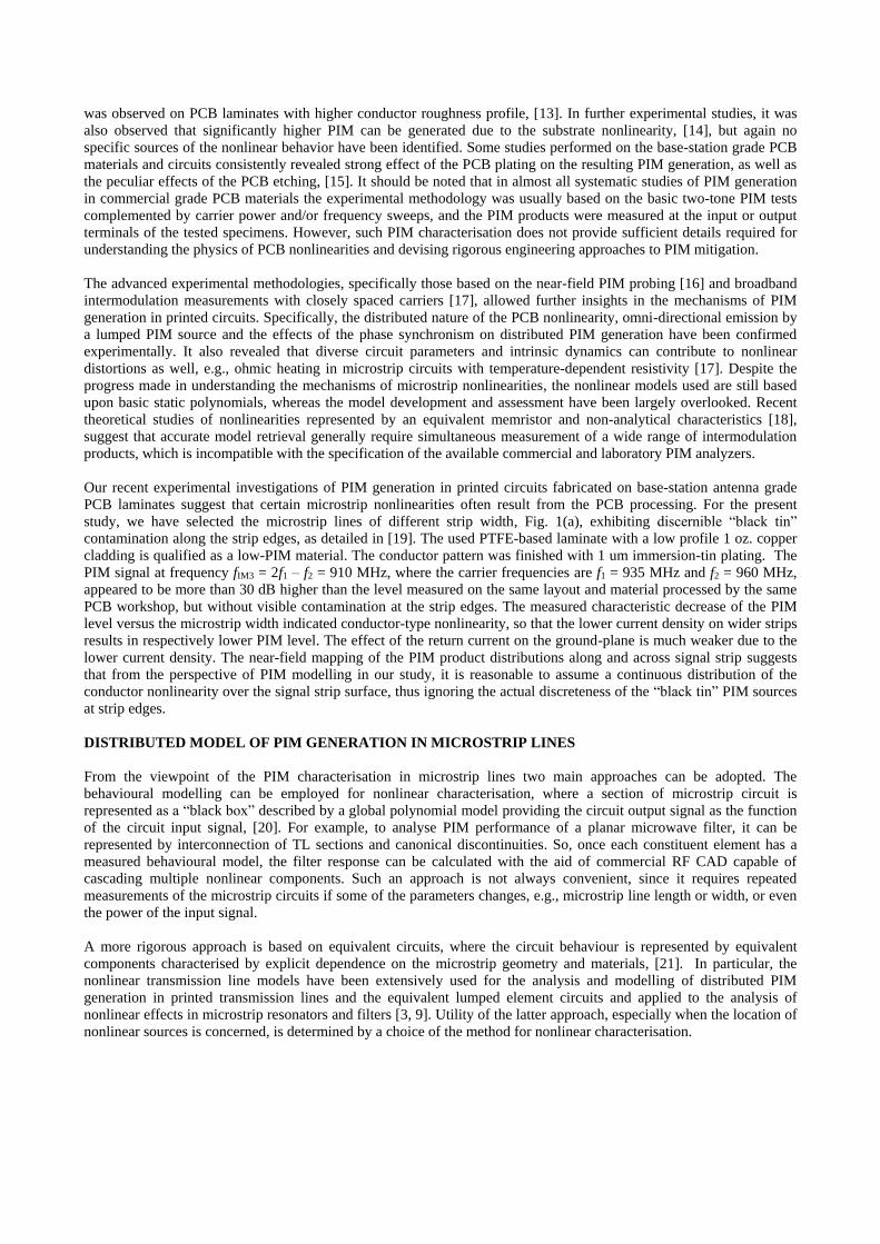
In this study, we use the harmonic balance solver and X-parameters for cascading nonlinear components in the Keysight
ADS software. For characterisation of microstrip nonlinearity, the model of a uniform microstrip line has been
implemented with the cascaded T-networks representing electrically short sections of a transmission line, so that the
effects of the TL discretisation be negligible. It was actually found that the short T-cells provide more accurate
description of the NLTL than the L-networks, although some authors suggest that an all-pass lattice filter topology suits
best for distributed nonlinear modelling, [24]. The TL nonlinearity model (1) has been retrieved for each test microstrip
line of specific width by fitting the simulated forward PIM3 products to the measurement data in a range of carrier
power values, see Fig. 2. It appears that the fitting accuracy strongly depends on the model order, so that a large number
of polynomial terms are required to achieve the residual error. This can be attributed to a systematic error in PIM
measurements. Also, the model proved to be sensitive to the carrier power, and an accurate prediction of higher order
PIM products from the PIM3 measurements requires even more polynomial terms.
(a) (b)
Fig. 2. (a) Nonlinear model (1) estimation for the uniform microstrip line in Fig. 1(a) by minimising the normalised
root-mean square deviation (RMSD) and (b) comparison of the estimated model with experimental data.
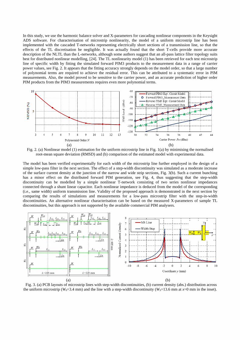
The model has been verified experimentally for each width of the microstrip line further employed in the design of a
simple low-pass filter in the next section. The effect of a step-width discontinuity was simulated as a moderate increase
of the surface current density at the junction of the narrow and wide strip sections, Fig. 3(b). Such a current bunching
has a minor effect on the distributed forward PIM generation, see Fig. 4, thus suggesting that the step-width
discontinuity can be modelled by a simple nonlinear T-network consisting of two series nonlinear impedances
connected through a shunt linear capacitor. Each nonlinear impedance is deduced from the model of the corresponding
(i.e., same width) uniform transmission line. Validity of the proposed approach is demonstrated in the next section by
comparing the results of simulations and measurements for a low-pass microstrip filter with the step-in-width
discontinuities. An alternative nonlinear characterisation can be based on the measured X-parameters of sample TL
discontinuities, but this approach is not supported by the available commercial PIM analysers.
(a) (b)
Fig. 3. (a) PCB layouts of microstrip lines with step-width discontinuities, (b) current density (abs.) distribution across
the uniform microstrip (W0=3.4 mm) and the line with a step-width discontinuity (WS=13.6 mm at x=0 mm in the inset).

(a) (b)
Fig. 4. Measured forward (a) and reverse (b) PIM3 products at 910 MHz on the “quality” microstrip lines in Fig. 3(a)
(NB: the “quality” lines do not show discernible “black-tin” edge contamination, in contrast to those in Fig. 1).
ANALYSIS AND DESIGN OF MICROSTRIP FILTERS UNDER LINEARITY CONSTRAINTS
The semi-phenomenological model of microstrip nonlinearities outlined in the preceding section is applied here to the
analysis of simple microstrip filters. Figure 5(a) shows the layout of a low-pass microstrip filter comprised of nine
sections of uniform microstrip lines of various widths and lengths, and eight step-width discontinuities. The filter has
been designed to be well matched in the E-GSM band (880 - 960 MHz). The filter and test coupons of microstrip lines
and discontinuities are fabricated on one panel of the PCB laminate. Simulated and measured forward and reverse PIM3
products of the test filter versus input carrier power are shown in Fig. 5(b). The results are in good agreement. The
magnitudes of the simulated and measured PIM3 products have ~3 dB offset, which is likely to be caused by fabrication
tolerances leading to a small disparity of the nonlinear parameters of the printed filter and test coupons. Another reason
for the observed discrepancy could be attributed to the greater difference between the measured and simulated PIM3
responses on the narrow microstrip sections - the model limitation that was also observed in our previous studies.
(a) (b)
Fig. 5. (a) PCB layout of the low-pass filter and (b) its measured and simulated PIM3 products versus carrier power, P0.
Obviously, minimising the PIM response in planar filters by adjusting the printed layout is always prone to degrading
the small-signal performance, [3]. In order to assess how much improvement could be achieved and what implications
are for the filter parameters, simulations have been conducted for a three-stub Chebyshev bandpass filter shown in Fig.
6(a). The variable circuit parameters are summarised as in Table 1 for the given circuit size constraint.
Table 1. Simulated low-pass microstrip filter layouts
Layout θp1, deg. θp2, deg. θs, deg. Zs, Ω Zp1, Ω Zp2, Ω
I 70 76.5 130 50 42.05 21.02
II 80 82.5 107 41.9 42.05 21.02
III 90 90 90 40.2 42.05 21.02
IV 100 98.5 75 41.5 42.05 21.02
V 110 107 60 45 42.05 21.02

(a)
(b)
Fig. 6. (a) Equivalent circuit model of a three-stub bandpass filter and (b) its small-signal frequency response.
The nonlinear products generated in the considered filters were simulated using the ADS Harmonic Balance solver. The
simulated forward and reverse PIM3 products at frequency fIM3 = 2f1 − f2 = 910 MHz generated by two CW signals of
power 43 dBm and frequencies f1 = 935 MHz and f2 = 960 MHz are presented in Fig. 7(a). The results show that up to
8 dB reduction of the PIM3 level is achievable without noticeable change of the filter loaded Q. However, the filter
band edges are significantly affected. The sharper roll-off at the passband upper edge correlates with the higher PIM,
yet it is not clear without additional simulations which stub contributes most to the total PIM response. The simulation
results of the in-band PIM3 product with the carrier frequency f1 fixed and f2 swept are shown in Fig. 7(b). Notably, the
PIM3 level peaks at the band edges, with the higher level at the upper end corresponding to the sharper roll-off. One can
speculate whether the section with the highest resonance frequency is responsible for the PIM3 peaking at the high
frequency skirt, but predictions of our model proved to be fully consistent with the numerical analysis in [3]. The
presented results are subject to further experimental verification, which requires implementation of the controlled
distributed nonlinearity throughout the manufacturing process.
(a) (b)
Fig. 7. (a) Simulated out-of-band PIM3 for the different microstrip filter layouts (see Table 1 for the reference p1) and
(b) simulated in-band PIM3 for the filter layout III in Table 1 and Fig. 6.
CONCLUSIONS
In this paper, we have presented a consistent approach to the nonlinear model assessment by means of conventional
two-tone PIM measurements and efficient RF CAD simulations. Although the closed-form theoretical analysis can
provide valuable insights in the effects of the physical and geometrical parameters, the underlying assumptions are often
difficult to validate. Besides, analytical complexity rapidly grows for non-uniform and resonant circuits, which warrants
the development of a more efficient empirical means of PIM characterisation and modelling. To that end, the RF CAD
approach has been proposed to facilitate the nonlinear characterisation and PIM analysis of arbitrary circuit layouts and
signals. Two examples of the microstrip filters based on the step-width discontinuities and shunt stubs have been
presented and the simulation results confirm that PIM reduction is achievable by careful selection of the microstrip
layout without frustrating the small-signal performance. Moreover, the presented simulation results are in a very good
agreement with the experiments and published works, which suggests feasibility of improved PIM control in the future.

ACKNOWLEDGEMENTS
This work has been carried out in the framework of Marie Curie European Industrial Doctorate (EID) programme
ARTISAN jointly with Bell Labs Ireland, grant No. 316426. The authors wish to thank Mr Christian Entsfellner and
staff at Rosenberger Hochfrequenztechnik GmbH & Co. KG for support with the key measurement facilities and Dr
Efstratios Doumanis for very fruitful discussions of the filter design and characterisation.
REFERENCES [1] M.A. Megahed and S.M. El-Ghazaly, “Nonlinear analysis of microwave superconductor devices using full-wave
electromagnetic model,” IEEE Trans. MTT, vol. 43, no. 11, pp. 173 – 178, 1995. [2] O.G. Vendik, I.B. Vendik, and T.B. Samoilova, “Nonlinearity of superconducting transmission line and microstrip
resonator,” IEEE Trans. MTT, vol. 45, no. 2, pp. 173 – 178, 1997. [3] T. Dahm and D. Scalapino, “Analysis and optimisation of intermodulation in high-Tc superconducting microwave
filter design,” IEEE Trans. Appl. Supercond. vol. 8, no. 4, pp. 149 - 157, 1998. [4] D. Seron, et al., “Analysis and simlation of distributed nonlinearities in ferroelectrics and superconductors for
microwave applications,” IEEE Trans. MTT, vol. 54, no. 3, pp. 1154 - 1160, 2006. [5] A. Kozyrev, et al., “Ferroelectric films: nonlinear properties and applications in microwave devices,” IEEE MTT-
S Int. Microw. Symp. Digest, 1998, pp. 985 – 988. [6] F. Gölden, “Liquid crystal based microwave components with fast response times: material, technology, power
handling capability,” Ph.D. dissertation, Technische Universität Darmstadt, Darmstadt, 2010. [7] M.I. Salkola, “Intermodulation response of superconducting filters,” J. Appl. Phys., vol. 98, 023907, 2005. [8] J. Mateu, et al., “Nonlinear performance characterization in an eight-pole quasi-elliptic bandpass filter,”
Supercond. Sci. Technol., vol. 17, pp. 359 – 362, 2004. [9] S.M.H. Javadzadeh, et al., “Nonlinear circuit model for discontinuity of step in width in superconducting
microstrip structures and its impact on nonlinear effects,” IEEE Trans. on Appl. Supercond., vol. 23, no. 2, 2013. [10] O. G. Vendik, and I. B. Vendik, “Power dependence of HTS disk-resonator quality factor,” IEEE Trans. MTT, vol.
46, no. 6, pp. 851 - 856, 1998. [11] J.J. Xia, J.A. Kong, and R.T. Shin, “A macroscopic model of nonlinear constitutive relations in superconductors,”
IEEE Trans. MTT, vol. 42, no. 10, pp. 1951 - 1957, 1994. [12] T. Dahm and D. Scalapino, “Theory of microwave intermodulation in a high-Tc superconducting microstrip
resonator,” Appl. Phys. Lett., vol. 69, 4248, 1996. [13] A.G. Schuchinsky, J. Francey, V.F. Fusco, “Distributed sources of passive intermodulation on printed lines”, IEEE
AP-S Int. Symp. / URSI Meeting, Washington D.C., 3-8 July 2005, vol. 4B, pp. 447-450. [14] A.P. Shitvov, et al., “Effects of geometrical discontinuities on distributed passive intermodulation in printed lines,”
IEEE Trans. MTT, vol. 58, no. 2, pp. 356-362, 2010. [15] B. El Banna, “Passive intermodulation from printed circuit boards,” Technical Report D1200002735, Powerwave
Technologies, June 2006. [16] A. Shitvov, et al., “Passive intermodulation generation on printed lines: near-field probing and observations,”
IEEE Trans. MTT, vol. 56, no. 12, pp. 3121 - 3128, 2008. [17] J.R. Wilkerson, et al., “Electro-thermal theory of intermodulation distortion in lossy microwave components”,
IEEE Trans. MTT, vol. 56, no. 12, pp. 2717-2725, Dec. 2008. [18] J. Sombrin, “Non-analytic at the origin, behavioral models for active or passive non-linearity,” Int. J. Microw.
Wireless Technol., vol. 5, no. 2, pp. 133–140, 2013. [19] A. Shitvov, et al., “RF CAD-Assisted Nonlinear Transmission Line Model of Distributed Passive
Intermodulation,” Proc. MULCOPIM 2017, ESA/ESTEC Noordwijk, The Netherlands, 5-7 April 2017, (accepted) [20] A.P. Shitvov, et al., “Communication nonlinearities techniques for characterisation of passive intermodulation,” in
Proc. MULCOPIM’ 2014, 17-19 September 2014, Valencia, Spain. [21] D. E. Zelenchuk, et al., “Passive intermodulation in finite lengths of printed microstrip lines,” IEEE Trans. MTT,
vol. 56, no. 11, Part 1, pp. 2426-2434, 2008. [22] K.R. Carroll, et al., “Superconducting kinetic-inductance microwave filters,” IEEE Trans. Appl. Supercond., vol.
3, no. 1, pp. 8-16, 1993. [23] A.R. Djordjevic and T.K. Sarkar, “Closed-form formulas for frequency-dependent resistance and inductance per
unit length of microstrip and strip transmission lines,” IEEE Trans. MTT, vol. 42, no. 2, pp. 241 – 248, 1994. [24] S. Paul, K. Hüper, and J.A. Nossek, “Models for nonlinear transmission lines,” in Proc. ISCAS'93, Chicago IL, 3-6
May 1993, vol. 4, pp. 2287 – 2290.


![Microwave Microstrip Tunable Bandpass Filters – technology ... planar... · Equivalent circuits of the varactor tuned combline ... [35], the noise figure of the active filter is](https://static.fdocuments.in/doc/165x107/5b4f6ebd7f8b9a256e8c4ede/microwave-microstrip-tunable-bandpass-filters-technology-planar-equivalent.jpg)