On-Chip Variation
48
On-Chip Variation (OCV)
-
Upload
kunal-ghosh-vlsisystemdesigncom -
Category
Technology
-
view
1.405 -
download
0
Transcript of On-Chip Variation

On-Chip Variation (OCV)

Ever thought what's an interviewer's favorite questions to rip you off - all of my previous post
:).
And On-Chip Variation (OCV) is one of them, specifically for Static Timing Analysis
interview. This analysis is coming from people who got interviewed and recruited into leading
VLSI industries.
Most importantly, my posts and videos have helped most of them and I really feel proud
about it. Nice feeling.
Coming back to analyze OCV, the first task is to find all possible sources variation, and find out
how these can affect a delay of a cell and hence, timing.
First things first - Sources of variation1) Etching
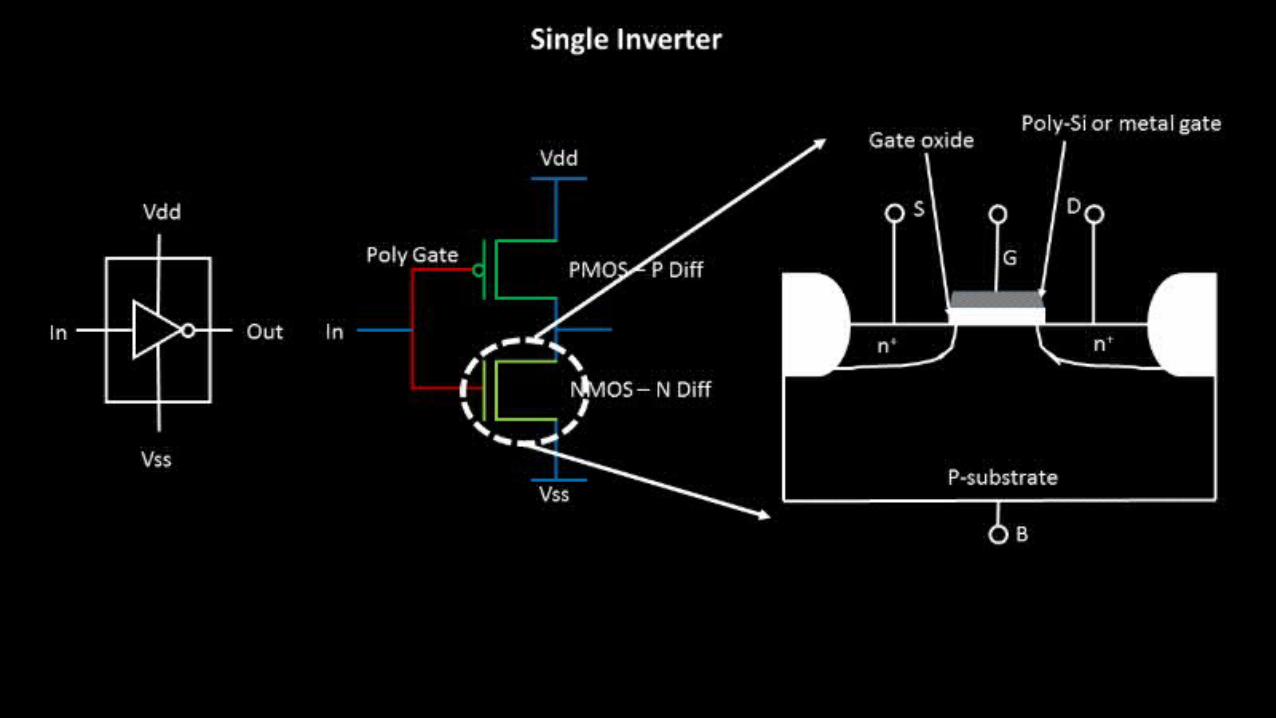
Look into the below layout of an inverter (which also shows the Width (W) and Length
(L) parameters of an inverter)


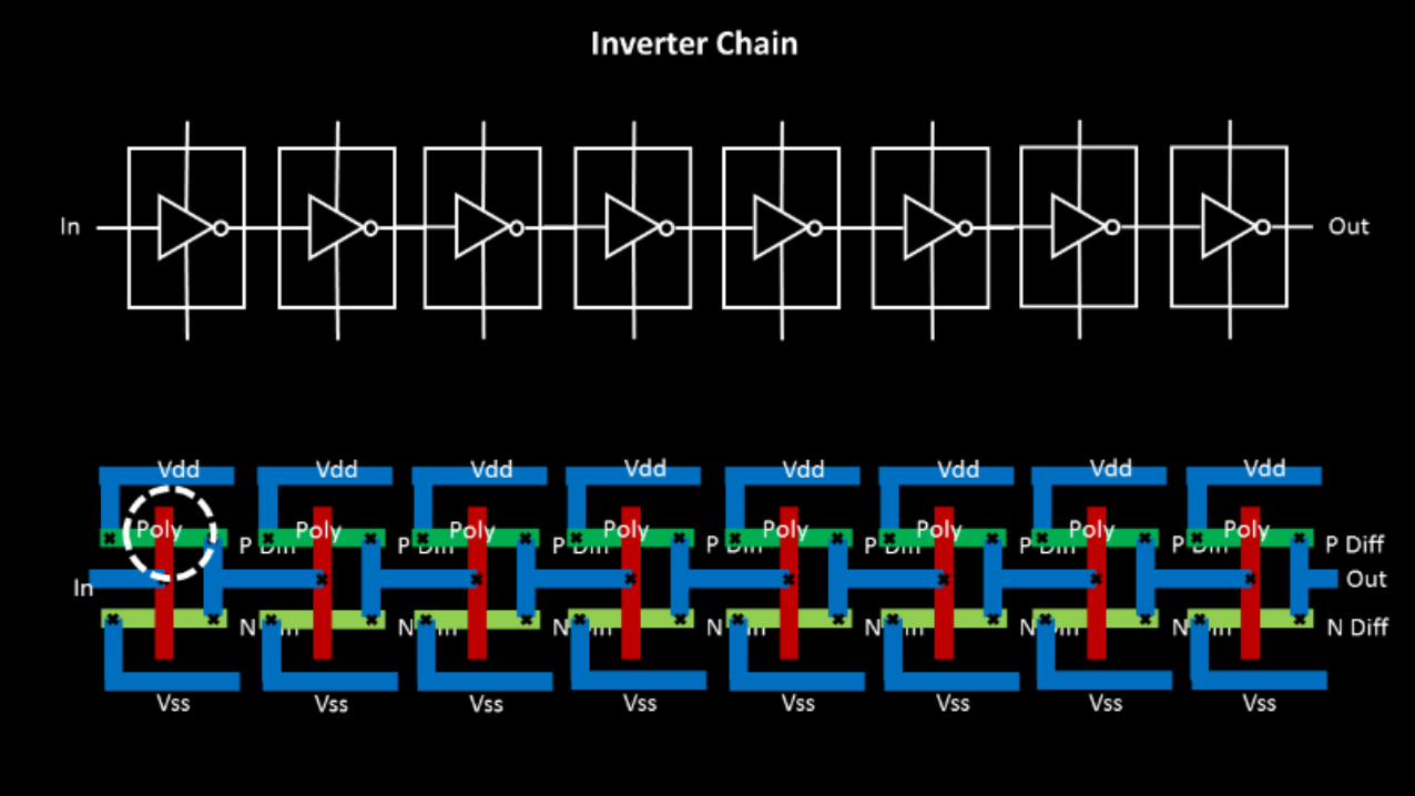
And, a chain of inverters (this is mostly the case of clock path, be with me for upcoming
posts and I will exactly let you know, why OCV is mainly applied on clock paths, 50% should be clear from the term "chain of inverters")

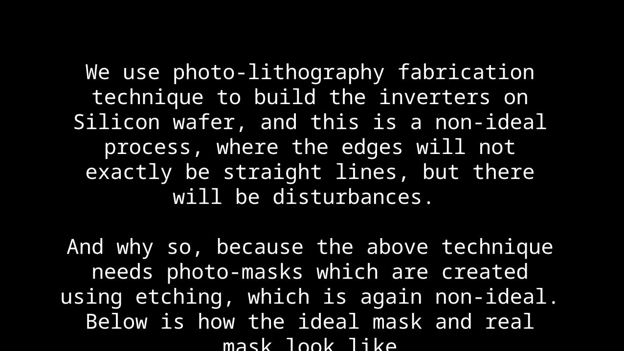
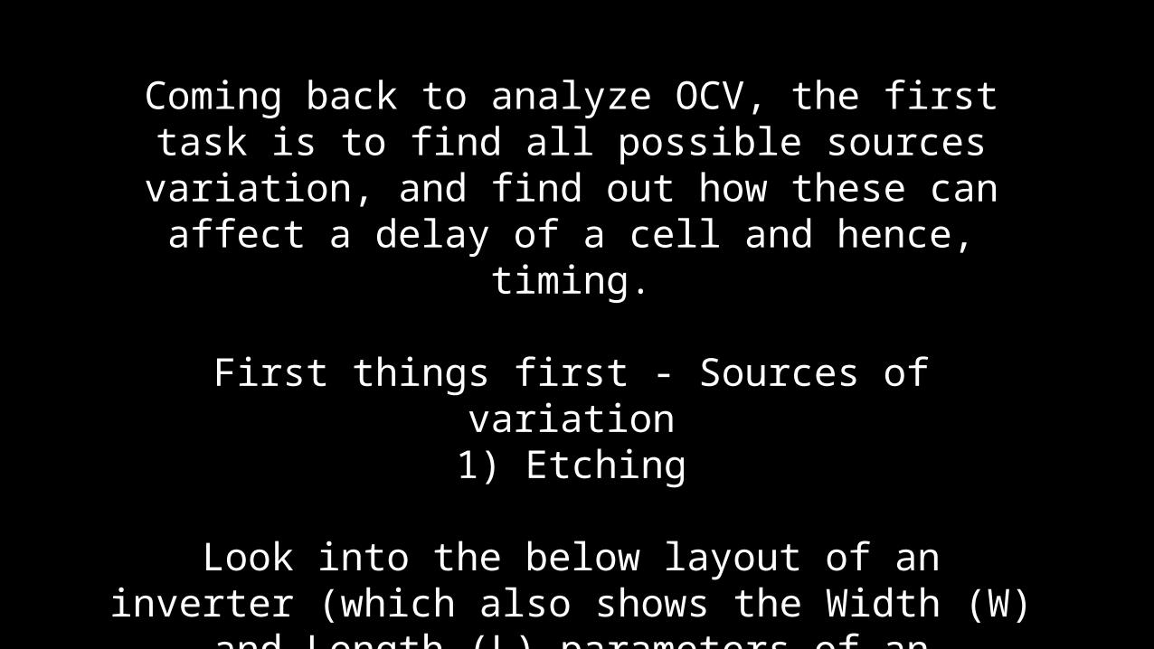
We use photo-lithography fabrication technique to build the inverters on Silicon
wafer, and this is a non-ideal process, where the edges will not exactly be straight lines, but
there will be disturbances.
And why so, because the above technique needs photo-masks which are created using
etching, which is again non-ideal. Below is how the ideal mask and real mask look like

Now these variations on the sides, is also dependent on what logic cell is present on
either sides of this inverter, if its surrounded by chain of inverters on either sides, the variation on the sides will be less as the
process parameters to build mask for a chain of similar size inverter, is almost the same.
But, if the inverters are surrounded by other gates, like flip-flops, then the variation will be
more.
With that said, the below inverters in the middle will have a similar and less
variations ......... (sentence continues after the below image)
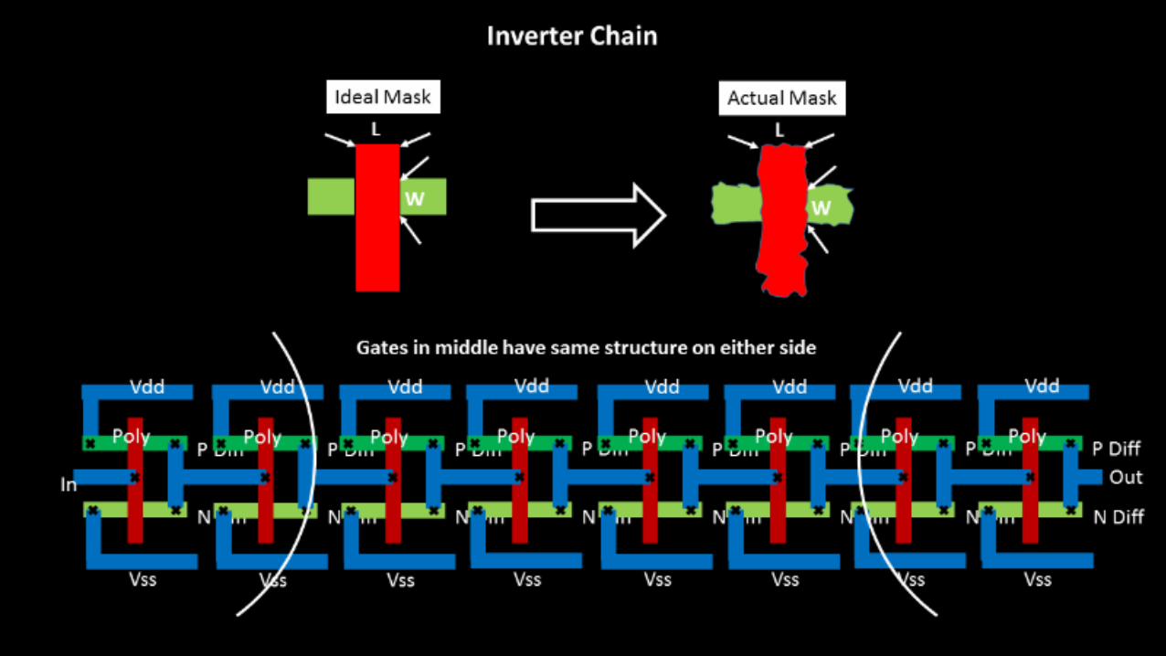
......(sentence continued from above) and the inverters on the boundaries will have different and more variations. (observe the difference in
actual mask, in below and above image)

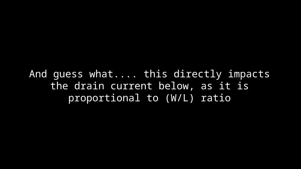
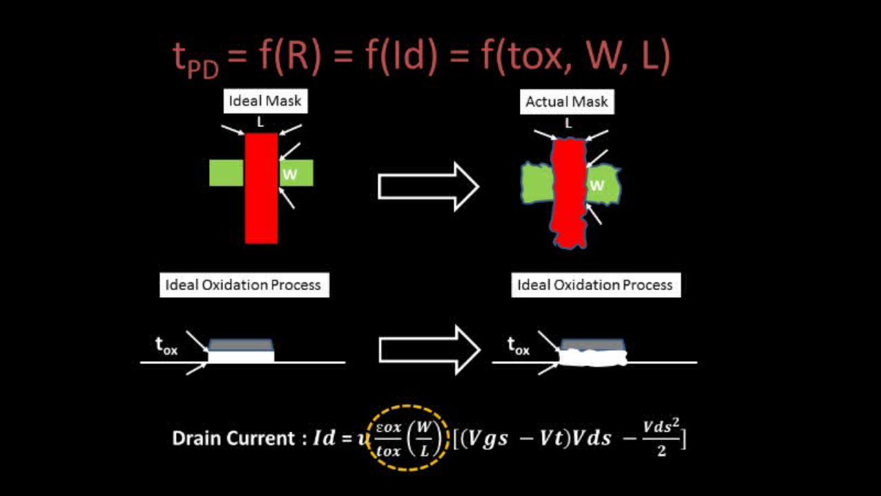
And guess what.... this directly impacts the drain current below, as it is proportional to
(W/L) ratio


You feel, we are almost there.... not yet....we need to identify other sources of variation, find out how the current changes, and eventually,
find out a range on what should be the value of OCV....
After this, do you feel, we are done .... not yet .... :), we need to use these OCV values,
plug it in STA analysis and see its (+ve or -ve) impact....

We were identifying sources of variations, and below is the second one
2) Oxide Thickness
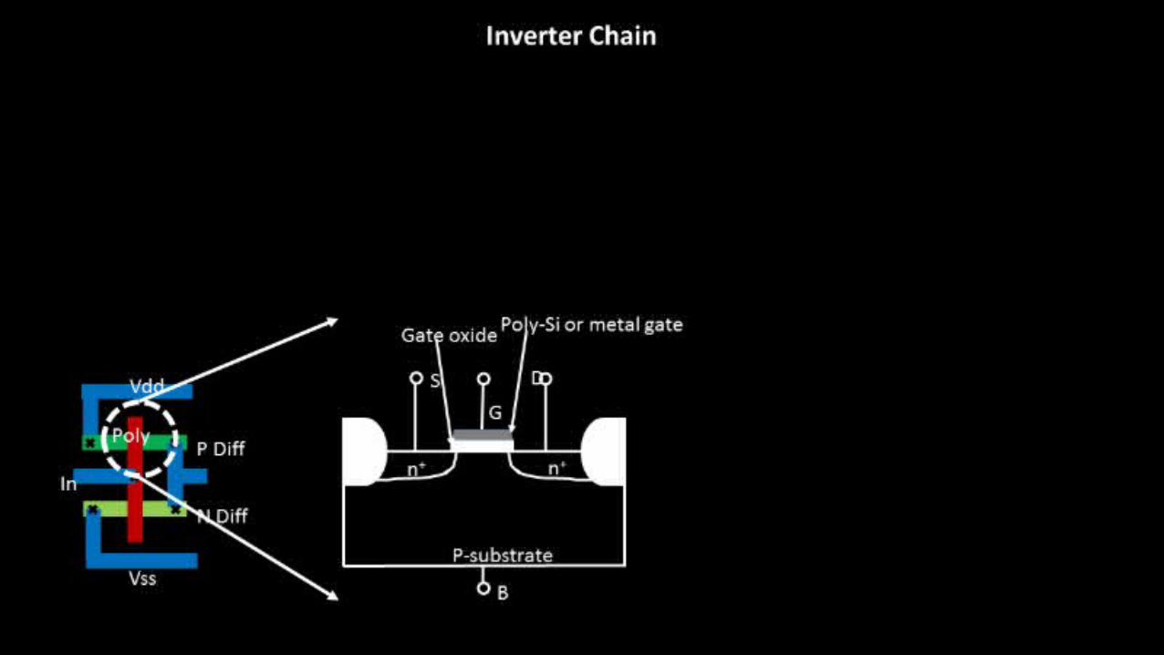
Let's go back to the inverter layout and look which part are we talking about

Here, we are talking about gate oxide thickness variation
Below is the section from inverter chain, which we are worried about

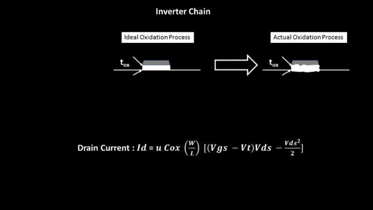
If we go by ideal fabrication process, below is what you will achieve, a perfectly cubic shape (below is the 2D image, so it looks rectangle)
oxide layer, and perfectly deposited metal gate or polysilicon gate


But, if we go by actual oxidation process, its very difficult or almost impossible to achieve
the above perfect oxide thickness.
And I can confidently say that, as I have worked on fabrication for a brief period of time
during my Masters at IIT Bombay.
Below is what you will actually get


So, what's wrong having above oxide thickness.
Again, its the drain current (which is a function of oxide thickness, shown in below image) that
will get varied for the complete chain of inverter, especially, the one's on the sides.
The variations in middle inverters will still be uniform. We discussed the reason for this in
last post


Imagine a chain of, as long as, 40 inverters or buffers ..... the variation is HUGE. And this
needs to be accounted for, in STA.
So the challenge is, how to we find the range and effectively model it in STA. Are we
scared ? Of course Not .... :)
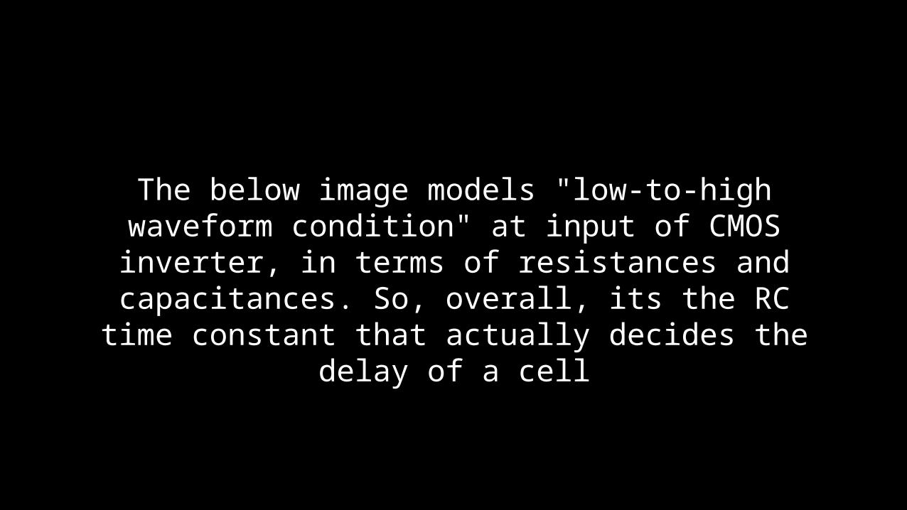
The below image models "low-to-high waveform condition" at input of CMOS
inverter, in terms of resistances and capacitances. So, overall, its the RC time
constant that actually decides the delay of a cell
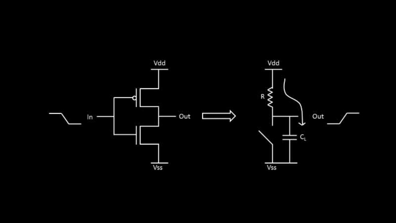


With above, we can safely say, the propagation delay tPD is a function of 'R'


Now, from previous posts, we seen variation in drain current 'Id' due to variation in 'W/L' and 'oxide thickness' variations, and above we see,
how propagation delay is function of 'R'.
The question is now, what next?.
If I am, somehow, able to prove, that drain current 'Id' strongly depends on 'R', then I can
directly relate (W/L) and oxide thickness variation to 'R', and below images will exactly
do that

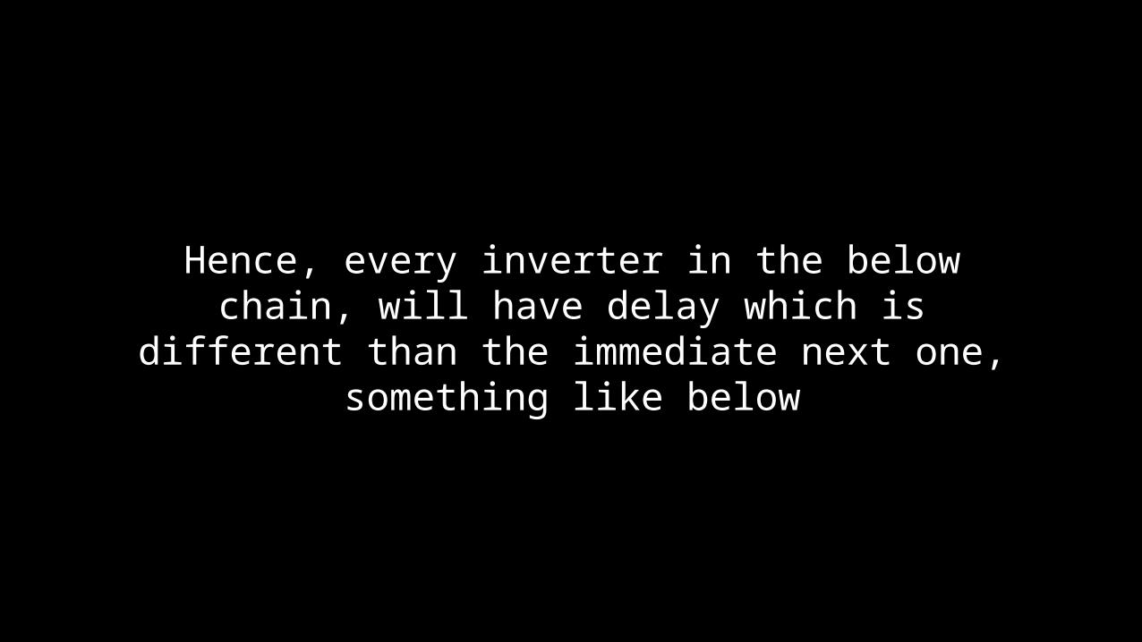
Hence, every inverter in the below chain, will have delay which is different than the
immediate next one, something like below
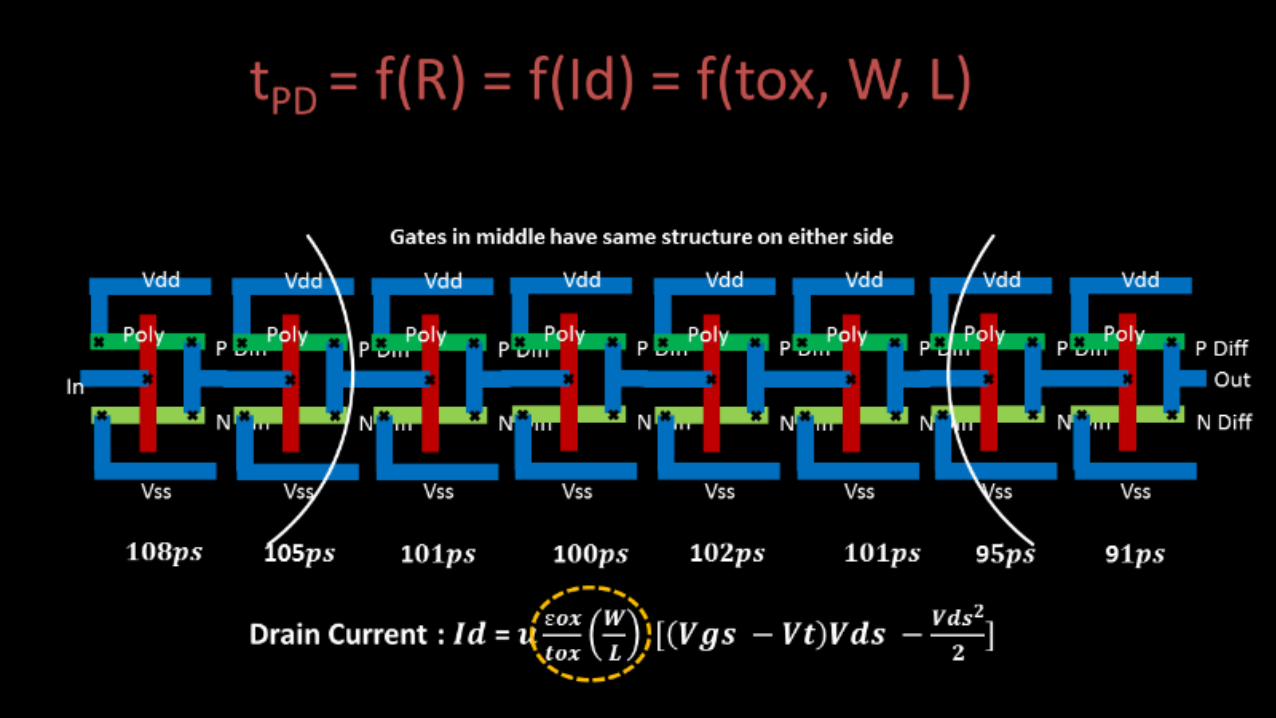

If we plot a Gaussian Curve with delays on x-axis and no. of inverters on y-axis, it will give us a clue, about the peak variation in inverter
delays, the minimum and maximum variation in inverter delays like below
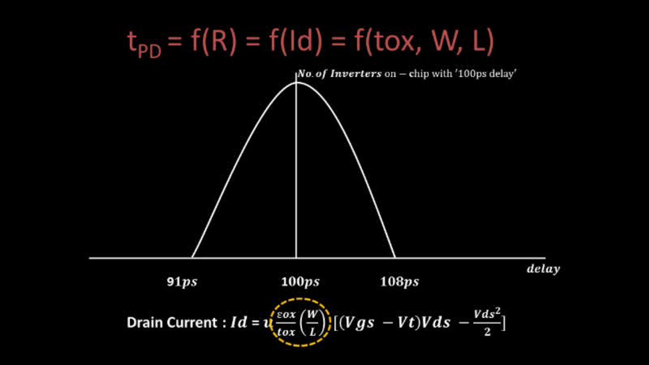

Now, we know the percentage variation in delays of inverter compared to '100ps',
because that's where the inverter delay (with used 'W/L' ratio) is expected to be, and most number of inverters on chip with that 'W/L'
ratio have a delay of 100ps

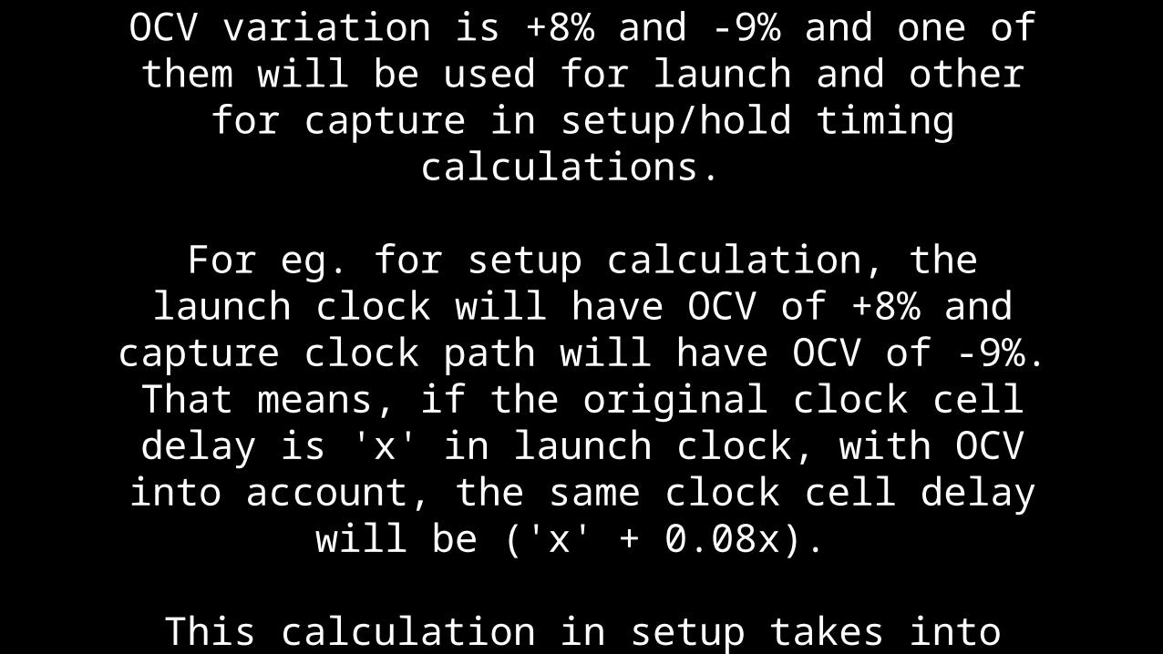
OCV variation is +8% and -9% and one of them will be used for launch and other for capture in
setup/hold timing calculations.
For eg. for setup calculation, the launch clock will have OCV of +8% and capture clock path
will have OCV of -9%. That means, if the original clock cell delay is 'x'
in launch clock, with OCV into account, the same clock cell delay will be ('x' + 0.08x).
This calculation in setup takes into account the On-Chip Variation, and that's where the name
comes from, as shown below

The images in above ppt makes this concept so simple. Isn't it? But, keeping things simple is
the most difficult job :) I took around 3 weeks, just to make these images. Please ... kudos to
ME :) :).
For me, solving any concept, is just like a war. Ulysses S. Grant rightly mentions "The art of war is simple enough. Find out where your enemy is. Get at him as soon as you can. Strike him as hard as you can, and keep
moving on"

For more, please refer to below courses
Circuit design & SPICE simulationshttps://www.udemy.com/vlsi-academy-circuit-design/?couponCode=forSlideshare
Physical design flowhttps://www.udemy.com/vlsi-academy-physical-design-flow/?couponCode=forSlideshare
Clock tree synthesishttps://www.udemy.com/vlsi-academy-clock-tree-synthesis/?couponCode=forSlideshare
Signal integrityhttps://www.udemy.com/vlsi-academy-crosstalk/?couponCode=forSlideshare
VLSI – Essential concepts and detailed interview guidehttps://www.udemy.com/vlsi-academy/?couponCode=forSlideshare
THANK YOU