OFCOM · 5 INTERFERENCE AFFECTSON AND BY VARIOUS ... Filter stop-band rejection 60dBc ... By...
86
OFCOM Study of current and future receiver performance Appendices Lewis Davies Paul Winter 11 th January 2010 ©TTP 2010 company confidential
-
Upload
trinhduong -
Category
Documents
-
view
226 -
download
3
Transcript of OFCOM · 5 INTERFERENCE AFFECTSON AND BY VARIOUS ... Filter stop-band rejection 60dBc ... By...

OFCOM Study of current and future receiver performance Appendices Lewis Davies
Paul Winter
11th January 2010
©TTP 2010 company confidential

20/2009 Interim Report Issue 1 ©TTP 2010 company confidential CONTENTS
1 SELECTIVITY PRACTICAL EXAMPLE 1 1.1 DVB-T broadcast 1 1.2 Proposed receiver 1 1.3 Receiver performance 1 2 EXAMPLES FOR NEEDING BETTER CHANNEL SELECTIVITY 7 3 FACTORS THAT INFLUENCE THE REQUIRED RADIO SELECTIVITY 9 4 RECEIVER REQUIREMENTS FOR GOOD SELECTIVITY 11 4.1 Receive channel filter 11 4.2 Receiver linearity 11 4.3 Spurious responses 14 4.4 Sampling and analogue to digital conversion 15 4.5 Phase noise and reciprocal mixing 19 4.6 Receiver sensitivity 21 4.7 Receiver dynamic range 22 4.8 Transmit adjacent channel power leakage 23 4.9 Summary 23 5 INTERFERENCE AFFECTS ON AND BY VARIOUS MODULATION
TYPES 26 5.1 Bandwidth effects 26 5.2 Amplitude Modulation AM 26 5.3 Frequency modulation FM 27 5.4 GMSK as used in GSM 27 5.5 WCDMA 28 5.6 OFDM 30 6 RECEIVER ARCHITECTURES 33 6.1 Super heterodyne 33 6.2 Zero IF receiver 40 6.3 Low IF receiver 43 6.4 Architecture comparison 49 7 SILICON PROCESSES 52 7.1 RF NFET Key Device Parameters 53 7.2 CMOS Silicon-On-Insulator (SOI) 56 7.3 Integrated and discrete component comparison 57 8 KEY COMPONENTS 59 8.1 Band select filter 59 8.2 Low noise amplifier (LNA) 62 8.3 Mixer 64 8.4 Oscillators and quadrature generation 67
20/2009 Interim Report Issue 1 ©TTP 2010 company confidential CONTENTS
8.5 Discrete IF Filters 70 8.6 Integrated amplifiers and active filters 71 8.7 Analogue to digital convertors 78 8.8 Decimation 80

1
©TTP 2010 company confidential SELECTIVITY PRACTICAL EXAMPLE
1 SELECTIVITY PRACTICAL EXAMPLE This numerical example investigates the selectivity performance, with DVB-T blockers at 8 MHz (adjacent channel), 16MHz (alternate channel) and 80MHz away from the wanted signal, of a hypothetical receiver designed to receive DVB-T broadcasts. 1.1 DVB-T broadcast Channel spacing 8MHz Signal bandwidth (BW) 7.6MHz Modulation 64QAM 2/3 code 1.2 Proposed receiver
Architecture: Zero IF Input filtering: Tracking filter with 40MHz bandwidth Receiver Noise Figure: 5dB Input 3rd order intercept point: -10dBm C/N needed to decode a 64QAM 2/3 code signal: 18dB Local oscillator phase noise 90dBc/Hz at 10KHz offset Wideband local oscillator noise floor 150dBc/Hz Analogue filter: 3rd order with ±4MHz cut off Filter stop-band rejection 60dBc ADC effective resolution 9 effective bits ADC sample rate 80MSPS Digital filtering assumed perfect 1.3 Receiver performance The thermal noise floor of the receiver is:
= -174dBm + NF + 10 log BW = -174 + 5 + 69 = -100dBm The receiver sensitivity is:
= noise floor + C/N = -100dBm + 18dB = -82dBm In an ideal receiver the receiver’s noise figure would be near zero giving a theoretical receiver sensitivity of -87dBm.
A D
LNA tracking filter analogue filter mixer
DSP
analogue to digital convertor digital filter demodulator
LO

2
©TTP 2010 company confidential SELECTIVITY PRACTICAL EXAMPLE
1.3.1 8MHz adjacent channel selectivity Each of the factors which affect the receiver’s selectivity will initially be investigated separately. The blocker is assumed to be another DVB-T signal in the adjacent channel, with 8MHz channel spacing. Effects of the input filter – none Analogue filter
The filter rejection is very limited close to the carrier, but significantly greater further away from the wanted signal. The average filter attenuation is 9dBc for this blocker. ADC dynamic range
The ADC’s 9 bit (54dB) dynamic range can be partitioned as shown above. This leaves 22dB of the ADC’s range for blocking By combining the ADC blocking and analogue filter rejection the cascaded effect of the two can be determined to be 22 + 9 = 31dBc, i.e. taking no other receiver impairments into account the receiver adjacent channel selectivity can’t be any better than 31dB. With a redesign of the ADC, the ADC dynamic range could be up to 12 bits (72 dB dynamic range). With the same ADC partitioning and analogue filter as above, and perfect digital filtering, up to 49dB of adjacent channel selectivity can be obtained. Reciprocal mixing
zero IF receiver wanted centred on 0Hz
cut off frequency - 4MHz
~3dB
29.5dB
4 12
3rd order filter 60dB/decade slope
f (log scale)
4 12
C/N=18dB
RX imperfections, e.g. AGC, DC offsets~4dB
OFDM peak to average ratio ~10dB
blocking
Δω
Δω2, 6dB per octave
3
©TTP 2010 company confidential SELECTIVITY PRACTICAL EXAMPLE
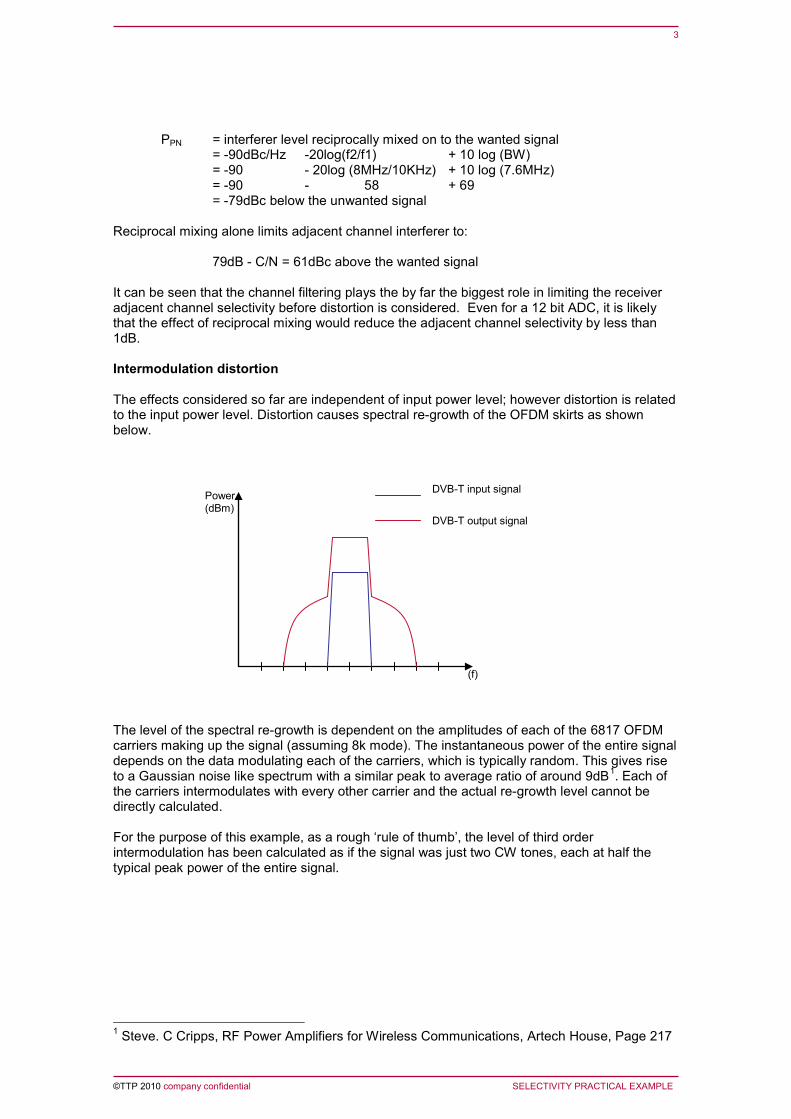
PPN = interferer level reciprocally mixed on to the wanted signal = -90dBc/Hz -20log(f2/f1) + 10 log (BW) = -90 - 20log (8MHz/10KHz) + 10 log (7.6MHz) = -90 - 58 + 69 = -79dBc below the unwanted signal Reciprocal mixing alone limits adjacent channel interferer to:
79dB - C/N = 61dBc above the wanted signal It can be seen that the channel filtering plays the by far the biggest role in limiting the receiver adjacent channel selectivity before distortion is considered. Even for a 12 bit ADC, it is likely that the effect of reciprocal mixing would reduce the adjacent channel selectivity by less than 1dB. Intermodulation distortion The effects considered so far are independent of input power level; however distortion is related to the input power level. Distortion causes spectral re-growth of the OFDM skirts as shown below.
The level of the spectral re-growth is dependent on the amplitudes of each of the 6817 OFDM carriers making up the signal (assuming 8k mode). The instantaneous power of the entire signal depends on the data modulating each of the carriers, which is typically random. This gives rise to a Gaussian noise like spectrum with a similar peak to average ratio of around 9dB1
1 Steve. C Cripps, RF Power Amplifiers for Wireless Communications, Artech House, Page 217
. Each of the carriers intermodulates with every other carrier and the actual re-growth level cannot be directly calculated. For the purpose of this example, as a rough ‘rule of thumb’, the level of third order intermodulation has been calculated as if the signal was just two CW tones, each at half the typical peak power of the entire signal.
DVB-T input signal
DVB-T output signal
Power (dBm)
(f)

4
©TTP 2010 company confidential SELECTIVITY PRACTICAL EXAMPLE
The intermodulation products will be generated in the wanted channel adding interference to the wanted received signal. As the receiver has an adjacent channel rejection of 31dB and requires an 18dB C/N, the noise floor, generated principally by the quantisation noise of the ADC, must be at least 49dB below the unwanted carrier. With an unwanted signal level of –43dBm the intermodulation distortion is also 49dB below the unwanted. The noise and distortion, at equal power levels, will combine incoherently reducing the overall adjacent channel rejection by 3dB.
With lower adjacent channel power levels the effect of distortion will be less. At higher power levels the effects of distortion will rapidly rise. In practice AGC can be used to limit the effects of the large signal by reducing the receiver gain. However as the receiver IP3 improves the receiver noise figure degrades. With ideal negative feedback, the receiver would not generate any intermodulation until the voltage range of the amplifier was exceeded. Assuming this was 1Vpk to pk, and the receiver had an input impedance of 50Ω, signals of up 4dBm could be handled without any distortion. With signals above 1V distortion would rise rapidly and cause wideband interference. If the same ideal receiver had no noise figure, and therefore had a sensitivity of -87dBm, was not limited by filter rejection or reciprocal mixing, a dynamic range of 88dB could be obtained.
f
ACR=31dB (from filter & ADC calculations)
Min C/N = 18dB
Power (dBm)
-43
-74
-92
-100
-140
-120
-100
-80
-60
-40
-20
0
-60 -50 -40 -30 -20
RMS Input power (dBm)
Inte
rfer
ence
(dB
m)
5
15
25
35
45
55
65
75
Inte
rfer
ence
(dB
c)
interference level (dBm)relative inteference level (dBc)

5
©TTP 2010 company confidential SELECTIVITY PRACTICAL EXAMPLE
Thus, without AGC or negative feedback, a blocker at -43dBm would have the same individual effect as ADC quantisation with ENOB of 9 bits. Combining the two, adjacent channel selectivity would be 28dB at this input level. For higher input levels intermodulation will dominate. 1.3.2 16MHz alternate channel selectivity Again the input filter has no effect. With a 16 MHz offset blocker, i.e. an alternate channel signal, the receiver’s analogue filter will be reasonably effective, giving an average power rejection of 33dB.
With the ADC giving an additional 22dB of dynamic range the alternate channel rejection is 55dB before distortion or reciprocal mixing is considered. With the interferer 16MHz offset from the wanted, the LO phase noise has reached its limit of 150dBc/Hz. Therefore the power of the reciprocal mixed noise in the wanted band is
-150 + 10 log (BW) = -150 + 10 log (7.6M) = -150 + 69 = -81dB below the unwanted signal
This limits the interferer reaching the mixer to:
81 - C/N = 63dB above the wanted signal
This will cause less than 1dB degradation of the receiver selectivity calculated above. An oscillator’s noise floor far away from the carrier is determined by the oscillator’s amplifier’s gain and noise figure. A typical amplifier biased for oscillation might have again of 18dB and a noise figure of 6dB.
N0 = (-174 + 18 +6 ) dBm/Hz = -150dBc/Hz
If the oscillator produces 10mW of the power the carrier to noise ratio is given by: C/N= 10 –(-150) dBc/Hz = 160dBc/Hz This theoretical oscillator would provide 10 dB less reciprocal mixing than the one used in the TV receiver example above.
cut off frequency - 3.8MHz
41dB
4 12
3rd order filter 60dB/decade slope
f
29dB
6
©TTP 2010 company confidential SELECTIVITY PRACTICAL EXAMPLE
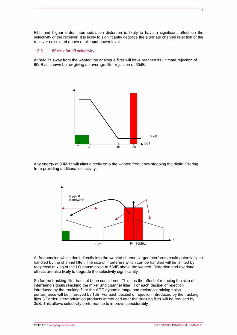
Fifth and higher order intermodulation distortion is likely to have a significant effect on the selectivity of the receiver. It is likely to significantly degrade the alternate channel rejection of the receiver calculated above at all input power levels. 1.3.3 80MHz far off selectivity At 80MHz away from the wanted the analogue filter will have reached its ultimate rejection of 60dB as shown below giving an average filter rejection of 60dB.
Any energy at 80MHz will alias directly onto the wanted frequency stopping the digital filtering from providing additional selectivity.
At frequencies which don’t directly into the wanted channel larger interferers could potentially be handled by the channel filter. The size of interferers which can be handled will be limited by reciprocal mixing of the LO phase noise to 63dB above the wanted. Distortion and overload effects are also likely to degrade the selectivity significantly. So far the tracking filter has not been considered. This has the effect of reducing the size of interfering signals reaching the mixer and channel filter. For each decibel of rejection introduced by the tracking filter the ADC dynamic range and reciprocal mixing noise performance will be improved by 1dB. For each decibel of rejection introduced by the tracking filter 3rd order intermodulation products introduced after the tracking filter will be reduced by 3dB. This allows selectivity performance to improve considerably
4 40 log f
60dB
80
Nyquist Bandwidth
f Fs/2 FS= 80MHz

7
©TTP 2010 company confidential EXAMPLES FOR NEEDING BETTER
CHANNEL SELECTIVITY
2 EXAMPLES FOR NEEDING BETTER CHANNEL SELECTIVITY 2.1.1 Use of spectrum cleared by Digital Switch Over (DSO) A practical example for receivers benefitting from better channel selectivity includes the reuse of 128MHz UHF spectrum which has become available due to the switch from analogue to digital TV and clearing aeronautical radar from channel 36 and radio-astronomy from channel 38. Currently this spectrum is used by other TV services with a regionalised use of frequencies to minimise interference issues. This cleared spectrum will be in two blocks, anticipated to be channels 31 to 37 and channel 61 to 70. The upper band of cleared spectrum is likely to be reused by mobile broadband services. There is a risk, unless suitable steps are taken, of TV viewers in some areas suffering interference from the base stations of the mobile broadband networks. By improving the selectivity of the TV receiver it would be possible to limit the susceptibility of the TV receiver to interference from the mobile broadband network. 2.1.2 Efficient local area broadcasting adjacent to SFN networks Another example is the adjacent channel selectivity of DAB receivers, operating in a single frequency network (SFN), limiting the positioning and power levels of broadcast transmitters. SFNs work well if each transmitter broadcasts all available multiplexes available in the area. This is shown in the first part of Figure 2-2 where local Multiplex B is broadcast from the same tower as national Multiplex A . However it is likely that the local radio operator’s transmission costs would be significantly lower if the multiplex was broadcast from a single transmitter tower. However as shown in the second part of figure 2-1, this would cause holes to be punched in the coverage areas of both broadcasters services. Improving the adjacent channel selectivity of the receiver would reduce the size of these holes.
Figure 2-2: Local DAB multiplex broadcast from one or two towers 2.1.3 Use of TDD networks Historically cellular systems have used FDD. In FDD all base-station transmitters transmit at one fixed set of frequencies for the downlink (base-station to mobile); and all mobile transmitters operator at another fixed set of frequencies for the uplink (mobile to base-station). For adjacent channel interference to occur in FDD, the interferer and victim must be of different equipment
Service area for mux B
Service area for mux A
Signal strength
Receiver adjacent channel selectivity
Receiver sensitivity
Mux A
Mux B
Multiplex B broadcast from single tower
mux A not available
mux B not available
mux B not available
Signal strength
mux A not available
mux B not available
mux B not available

8
©TTP 2010 company confidential EXAMPLES FOR NEEDING BETTER
CHANNEL SELECTIVITY
types, i.e. one is a mobile, whilst the other is a base-station. As base-stations always have some physical separation from mobiles, receivers can be used with a relatively low adjacent channel performance without limiting system performance. In addition, it also allows base-stations to be co-sited and mobile devices to be used in close proximity to each other without risk of adjacent channel interference. As it is not easy to change the uplink and downlink frequencies in FDD, it does imply that a fixed bandwidth is allocated to each. GSM and FDD UMTS both use this approach. In GSM the mobile is not required to transmit and receive at the same time. In FDD UMTS the receiver is required to receive at the same time as transmitting; just one of the measures used to increase the system spectral efficiency (bits/s/Hz/unit area). In TDD, time is used to divide the transmit and receive signals. The amount of time a handset needs to spend transmitting and receiving can vary depending on how it is being used. For two way speech it is likely to be symmetrical, for internet downloads it is likely to be highly asymmetrical. Advantages of TDD include permitting the use of ‘unpaired’ spectrum and allowing the spectrum to be used efficiently when the proportion of the uplink and downlink traffic varies. When TDD systems are operating in adjacent channels and are time synchronised, so that a receiver in close proximity to a transmitter operating on an adjacent channel is not expected to operate simultaneously to the transmitter, adjacent channel performance is generally similar to that required for FDD. However it is not always possible to time synchronise two adjacent TDD systems without losing spectral efficiency. In addition, parts of the spectrum allocated to UMTS TDD and potentially to LTE, lie next to FDD spectrum. Adjacent FDD and TDD carriers can’t be time synchronised. Currently much UMTS TDD spectrum throughout the world, owned by 120 UMTS operators, is underutilized2
2
.
http://www.iee-cambridge.org.uk/arc/seminar06/slides/AndrewWilliams.pdf [accessed 7th August 2009]

9
©TTP 2010 company confidential FACTORS THAT INFLUENCE THE
REQUIRED RADIO SELECTIVITY
3 FACTORS THAT INFLUENCE THE REQUIRED RADIO SELECTIVITY A radio must be able to receive the wanted signal with sufficient C/N0 in the presence of interfering signals, i.e. sufficient C/(N+I). The following example illustrates how a cellular and TV receiver have very different selectivity requirements. The C/N0 required for DVB-T, as used in terrestrial digital television broadcasting, is typically 18dB whilst for GSM, as used in many mobile phones, it is around 9dB. The level and number of interferers reaching the radio has a large influence on the selectivity requirements of the radio itself. Receiver location, frequency, antenna position and gain all influence this. For instance:
• If the radio is located in an environment near a large number of transmitters, especially high power ones, several significant interferers can be expected to be received. For DVB-T, TV effective isotropic transmit powers (EIRP), post DSO, of up to 200KW are likely to be used. This power will be continuous. For cellular, EIRP levels of up to 1.5KW are permitted3
. The actual power level will depend on the loading on the base-station and its position.
• The antenna position and gain will have a massive influence on the number and size of interferers reaching the receiver. For example if a GSM cellular phone operating at around 915MHz is compared with a TV operating at up to 860MHz the frequencies are fairly similar. However the TV receiver will probably use a high gain antenna mounted on a roof at around 10m above ground level whilst the GSM phone will be hand held and may be indoors. This difference could easily account for power levels of a common interferer reaching the TV receiver to be 30dB greater than those reaching the GSM receiver.
• The TV antenna may have 10dBi of gain whilst the GSM phone is likely to have an
antenna gain of less than 0dBi. When combined with the different antenna positions this will lead to the same interfering signal reaching each receiver with a 40dB difference. Both systems are expected to work with the power of the respective wanted signals only a few decibels above the noise floor. The only mitigating factor is that the TV receiver antenna has directionality, so the 10dB of antenna gain only applies to signals originating from the direction the antenna is pointing. In other directions the antenna will effectively attenuate interfering signals.
[[I really don’t understand what this shows.]] Figure 3-1: Comparison of RF signals at the input to a TV and GSM phone receiver used in the same location
3 Stewart, William, “Mobile Phones and Health,” IEGMP, May 2000
TV cellular
Signals at input to TV with roof mounted high gain antenna
f
Interferer to cellular and TV
TV cellular
Signals at input to GSM phone used indoors
f
Interferer to cellular and TV
~40dB

10
©TTP 2010 company confidential FACTORS THAT INFLUENCE THE
REQUIRED RADIO SELECTIVITY
In determining the receiver selectivity specification required for a particular system, the RF power levels and frequency of both the wanted signal and interferer reaching the receiver need to be considered. This requires the following factors to be considered:
• the receiver’s antenna position and gain; • the RF path loss between the transmitter and receiver for both the wanted and
unwanted signals; • the power of the transmitted signals for both the wanted and any interferers • the frequency relationship between the wanted and interfering signals; are they close
together or wide apart? It is relatively easy to build a receiver with good rejection of signals separated in frequency from the wanted signal, but much more difficult to reject interfering signals close to the wanted signal.
It is likely that to ensure that all potential users of the system are not affected by interference, an unreasonably high level of selectivity is required, perhaps making the system uneconomic. The system designer therefore needs to consider, in order for a reasonable number of users to not be affected by interference, what level of selectivity is required. As well as specifying the receiver selectivity, if the system designer can influence the network planning of the systems which could produce potential interferers, it may be possible to reduce the likelihood of these systems producing harmful interference to the victim system. For example, by co-siting the transmitters for two systems operating on adjacent channels, adjacent channel selectivity requirements can be minimised. The receiver selectivity specification required can be determined using two broad test cases, the selectivity required with a high level interferer and the selectivity required with a weak wanted signal. 3.1.1 Selectivity required with high level interferers In this case the following factors need to be considered:
• What are the highest level interferers likely to be received by the receiver? • What is the level of the wanted signal likely to be received simultaneously? • What is their frequency relationship?
If the receiver’s antenna is positioned in a location where it is picking up strong interfering signals, it is likely that it is also receiving the wanted signal reasonably strongly. 3.1.2 Selectivity required with a weak wanted signal In this case the following factors need to be considered:
• What is the lowest level of the wanted signal expected to be received? • What level of interferer is likely to be received simultaneously by the receiver? • What is their frequency relationship?
Typically the wanted signal is set 3dB above the minimum sensitivity level of the receiver so that the interference power equals the noise power. Traditionally, most radio transmitters, e.g. cellular base stations and TV transmitters have been located away from the receive antennas of the users equipment. In this situation, if the receiver’s antenna is positioned in a location where it is picking up only a weak wanted signal it is statistically likely that the interfering signals are also fairly weak. With the increase of radio transmitters within the home, for example Wi-Fi and Femto base-stations there is an increased likelihood of a transmitter very close to a receiver so whilst the wanted received signal may be weak, the interfering signal could be very strong.

11
©TTP 2010 company confidential RECEIVER REQUIREMENTS FOR GOOD
SELECTIVITY
4 RECEIVER REQUIREMENTS FOR GOOD SELECTIVITY This chapter investigates what receiver requirements are needed for good selectivity and why real world receivers may struggle to achieve the selectivity required for good system performance and spectrum use efficiency. 4.1 Receive channel filter With the exception of FFT based OFDM demodulation, a receiver’s demodulator tends to have little or no selectivity. Therefore, for the demodulator to be unaffected by out of band signals, these interfering signals need to be suppressed by the receiver to a level such that there is a sufficient C/N of the wanted signal at the receiver’s demodulator. , i.e.:
Filter rejection = minimum C/N required + required selectivity + 3dB
Ideally the receive channel filter should not affect the wanted signal. In practice the channel filter used is not ideal as shown in Figure 4-1. This may be due to the channel filter shape, ultimate out of band rejection, or due to frequency inaccuracies such as the receiver’s local oscillator mixing down the received signal to slightly the wrong frequency. Whilst too wide a filter will lead to inadequate suppression of adjacent channels, too narrow filtering will lead to suppression of the wanted signal leading to loss of signal and in some systems inter-symbol interference.
Figure 4-1: Effect of channel filter 4.2 Receiver linearity All analogue elements of a receiver such as amplifiers, mixers, and filters have some non linearity, not least because they have a maximum signal they can amplify. These non linearities introduce distortion to both the wanted and any unwanted signals. As will be shown below this can lead to the creation of new interfering distortion products occurring at new frequencies. If these occur at critical frequencies within the receiver, this will affect the SINR needed for an adequate C/N at the demodulator.
Remaining interfering signal
interfering signal
wanted
wanted
input signals
signal at demodulator
channel filter

12
©TTP 2010 company confidential RECEIVER REQUIREMENTS FOR GOOD
SELECTIVITY
The nonlinearities can be described by the expansion y(x) = k1f(x) + k2[f(x)]2 + k3[f(x)]3 + higher order terms where k1f(x) is the amplified version of the input signal. Whilst real world signals do not generally consist of carrier waves, great insight into linearity can be gained by considering two tones at ω1 and ω2. By charactering components’ response with two tones it allows their performance, for weakly non linear systems, to be clearly specified. Let f(x) consists of two sinusoidal signals close together in frequency: f(x) = A1 cos ω1t + A2 cos ω2t The second order products of the output are: y(x) = k2[f(x)]2
= k2 A1A2 [cos2 (ω1t) + cos2 (ω2t) + 2 cos (ω1t) cos (ω2t)] = k2 A1A2 [1 + ½ cos (2ω1t) + ½ cos (2ω2t) + cos ((ω1 + ω2)t) + cos ((ω1 - ω2)t) It can be seen that the second order products (known as second order intermodulation products, or IM2) are created at three frequencies, DC, f1 + f2 and f1 - f2. In terms of power level IM2 products are distributed against total IM2 power as:
• 50% (-3dB) at DC • 25% (-6dB) at f1 + f2 • 25% (-6dB) at f1 - f2
Second order products grow in proportion to the square of the input power. The third order products of the output are:
The third order IM3 products are created at 2f1 + f2, 2f1 - f2, 2f1 - f2 and 2f1 + f2. Assuming the non-linearity is frequency independent, all the third order terms are equal power. Third order products grow in proportion to the cube of the input power. The distribution of the 2nd and 3rd order intermodulation products is shown in Figure 4-2. For most analysis, where there are only mild non linearities, it is adequate to consider no more than third order products. It can be shown that when f1 and f2 are close together all higher even order products are formed at DC, at a low frequency dependent on the separation of f1 and f2, and at even multiples of f1 and f2. Also, it can be shown that all odd order products are clustered around f1 and f2.
[ ]
( ) ( ) ...+tω+ω2cos4
AAk3+tω+ω2cos
4AAk3
=
)t)ωcos(t)ωcos(AA+t)ωcos(t)ωcos(AA(k3=
)x(fk=y
121
223
212
213
221
2212
212
213
33
13
©TTP 2010 company confidential RECEIVER REQUIREMENTS FOR GOOD
SELECTIVITY
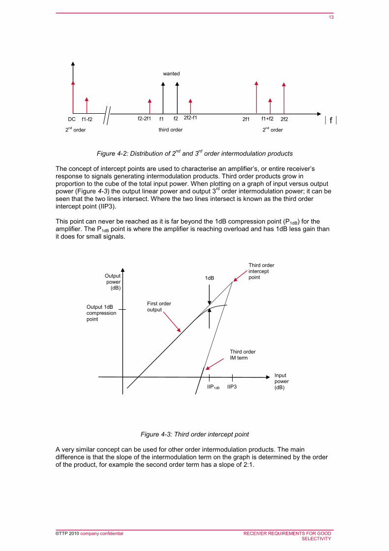
Figure 4-2: Distribution of 2nd and 3rd order intermodulation products The concept of intercept points are used to characterise an amplifier’s, or entire receiver’s response to signals generating intermodulation products. Third order products grow in proportion to the cube of the total input power. When plotting on a graph of input versus output power (Figure 4-3) the output linear power and output 3rd order intermodulation power; it can be seen that the two lines intersect. Where the two lines intersect is known as the third order intercept point (IIP3). This point can never be reached as it is far beyond the 1dB compression point (P1dB) for the amplifier. The P1dB point is where the amplifier is reaching overload and has 1dB less gain than it does for small signals.
Figure 4-3: Third order intercept point A very similar concept can be used for other order intermodulation products. The main difference is that the slope of the intermodulation term on the graph is determined by the order of the product, for example the second order term has a slope of 2:1.
f1 f2 2f2-f1 f2-2f1 │f│ f1+f2
third order 2nd order 2nd order
f1-f2 DC 2f1 2f2
wanted
1dB
IIP1dB IIP3
Output 1dB compression point
Output power
(dB)
Input power (dB)
Third order intercept point
Third order IM term
First order output

14
©TTP 2010 company confidential RECEIVER REQUIREMENTS FOR GOOD
SELECTIVITY
For convenience, intermodulation has been discussed by characterising component and receiver responses with two CW tones of equal power. In the real world a receiver is likely to receive multiple modulated interfering signals, all at varying power levels. Key differences are:
• Intermodulation products from multiple signals will cause a picket fence effect as each interferer intermodulates with every other interferer.
• The interferers may not be of equal power. The intermodulation product’s power depends on the total input power.
• The level of each product will depend on the instantaneous power, not the average power, of the interferers causing the product. For signals with a high peak to average ratio, the intermodulation product’s power levels will fall between that found if CW tones set to the peak powers or average powers were used in the determination. Unfortunately for the designer, the intermodulation product’s power levels will typically be much closer to that found from using the peak power rather than the average power.
• The bandwidth of each product will depend on the order of the intermodulation product as well as the bandwidth of the interfering signals.
Cross modulation is a particular type of 3rd order intermodulation. If a signal in an adjacent carrier is amplitude modulated, when viewed in the frequency domain it will have multiple spectral components. These components, when non-linearly amplified, will produce intermodulation products which fall in the wanted frequency band producing interference. In a real receiver multiple receiver stages are cascaded together. Intermodulation products developed in one stage are fed through to the next and therefore accumulate at each stage. As the relatively weak received signals are also generally amplified by each stage of a receiver, prior to demodulation, latter “back end” stages need to be able to better handle large signals than do the earlier “front end” stages. Good receiver intermodulation performance can be achieved by:
• Using back end stages with better large signal handling. • Filtering large interferers prior to the interfering signals reaching the back end stage
where they could cause problems. • Dynamically adjusting the amount of gain that front end stages have so that the size of
large interferers is limited so that they do not cause distortion in the back end stages. 4.3 Spurious responses Ideally amplifiers just amplify the signals and all higher order products are minimised. Mixers, on the other hand maximise the 2nd order sum (f1+f2) and difference (f1-f2) products. One of the mixer input frequencies is from a local oscillator (LO) allowing RF signals received at one frequency to be translated in frequency either up (up conversion) or down (down conversion) to another frequency. If the wanted signal at ωc+ ωif is mixed with a local oscillator at –ωc the sum of the signals is at ωif. At the same time any signals or noise at the “image” frequency ωc- ωif are also translated to ωif. This is known as a spurious response and is shown in Figure 4-4. The mixer’s amplitude response to the image product is identical to the wanted frequency. Handling the image frequency effectively is a critical part of receiver design as any signals at the image frequency will cause interference and degrade the receiver’s selectivity. How this image response is handled is the key difference in the various receiver architectures discussed in chapter 6.

15
©TTP 2010 company confidential RECEIVER REQUIREMENTS FOR GOOD
SELECTIVITY
Figure 4-4; Image products after downconverson In addition to the image response, mixers have other spurious responses at mfRF±nfLO. In many receiver designs it is possible to band pass filter the received signal before amplification so that the receiver only needs to deal with RF signals in a relatively narrow frequency band, limiting the number of spurious products which may be generated. Unwanted received signals at any frequency which modulate with the local oscillator or its harmonics, or with any signal present in the receiver (e.g. digital clocks) at another frequency, to form a product at the wanted received frequency, will be an issue degrading or completing blocking the reception of the wanted channel. Local oscillator harmonics can be a significant issue in wideband receiver designs such as TV tuners. 4.4 Sampling and analogue to digital conversion All digital receivers need to convert, or quantise, the received radio frequency analogue signal to digital samples. This requires the signal to be sampled using some form of analogue to digital convertor (ADC). Sampling is a very similar process to frequency mixing. In a mixer the input analogue signal is multiplied with the local oscillator. In an ADC the input analogue signal is multiplied with the sample clock. The Nyquist-Shannon sampling theorem states that if a function x(t) contains no frequencies higher than B Hertz, it is completely determined by giving its ordinates at a series of points spaced 1/(2B) seconds apart. The theorem shows that an analogue signal that has been sampled can be perfectly reconstructed from the samples if the sampling rate (fs) exceeds 2B samples per second, where B is the highest frequency in the original signal. Any frequency component above fs/2 is indistinguishable from a lower-frequency component, called an alias component, associated with one of the copies. The ADC’s Nyquist bandwidth is the frequency bandwidth over which the ADC can operate without forming alias components.
signals at input to receiver PSD
0 ω
-ωc
ω -ω ωc+ωif ωc-ωif -ωc+ωif -ωc-
down conversion after mixing
LO signal
wanted image
0 ω
ωif -ωif
16
©TTP 2010 company confidential RECEIVER REQUIREMENTS FOR GOOD
SELECTIVITY
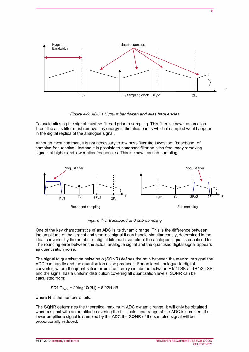
Figure 4-5: ADC’s Nyquist bandwidth and alias frequencies
To avoid aliasing the signal must be filtered prior to sampling. This filter is known as an alias filter. The alias filter must remove any energy in the alias bands which if sampled would appear in the digital replica of the analogue signal.
Although most common, it is not necessary to low pass filter the lowest set (baseband) of sampled frequencies. Instead it is possible to bandpass filter an alias frequency removing signals at higher and lower alias frequencies. This is known as sub-sampling.
Figure 4-6: Baseband and sub-sampling
One of the key characteristics of an ADC is its dynamic range. This is the difference between the amplitude of the largest and smallest signal it can handle simultaneously, determined in the ideal convertor by the number of digital bits each sample of the analogue signal is quantised to. The rounding error between the actual analogue signal and the quantised digital signal appears as quantisation noise. The signal to quantisation noise ratio (SQNR) defines the ratio between the maximum signal the ADC can handle and the quantisation noise produced. For an ideal analogue-to-digital converter, where the quantization error is uniformly distributed between −1/2 LSB and +1/2 LSB, and the signal has a uniform distribution covering all quantization levels, SQNR can be calculated from:
SQNRADC = 20log10(2N) ≈ 6.02N dB where N is the number of bits. The SQNR determines the theoretical maximum ADC dynamic range. It will only be obtained when a signal with an amplitude covering the full scale input range of the ADC is sampled. If a lower amplitude signal is sampled by the ADC the SQNR of the sampled signal will be proportionally reduced.
Nyquist Bandwidth
f Fs sampling clock Fs/2 3Fs/2 2Fs
alias frequencies
F Fs Fs/2 3Fs/2 2Fs F Fs Fs/2 3Fs/2 2Fs
Sub-sampling Baseband sampling
Nyquist filter Nyquist filter

17
©TTP 2010 company confidential RECEIVER REQUIREMENTS FOR GOOD
SELECTIVITY
In practice, effects such as distortion in the analogue section, jitter of the sampling clock and kT/C thermal noise introduced by the sampling switch, will create additional noise and spurious products reducing the dynamic range slightly. The ADC’s SNR is a practical measure of a real ADC’s maximum dynamic range. It characterises the ratio between the fundamental signal and the noise in the sampled spectrum. Often the Effective Number Of Bits (ENOB) of the useful signal data in the ADC’s output digital signal is used rather the SNR of the input signal. The ADC ENOB is always lower than the ADC’s headline number of bits of resolution. The ENOB and Nyquist bandwidth of an ADC must, at a minimum, be sufficient to handle the wanted signal. For instance, audio CDs are recorded with 16 bit resolution at a sampling rate of 44.1 KHz. This provides 96dB of dynamic range with a signal bandwidth of around 20 KHz. This is similar to the range of human hearing. Similarly the sampling rate of ADCs used in radio receivers must be at least the bandwidth of the received signal. The ENOB required will be discussed in section 4.4.2. 4.4.1 Automatic gain control An automatic gain control (AGC) system is a feed back control system typically used to control the gain of the receiver prior to sampling based on a power estimation of the sampled signal. For maximum dynamic range the amplitude of the input signal must cover the full scale input range of the ADC. Unlike analogue stages, where slightly overloading a stage causes some distortion to the wanted signal, ADCs hard limit and even a slightly larger signal than what the ADC can handle will result in a gross sampling error. By varying the gain of a preceding amplifier, an AGC loop allows the input signal’s amplitude to the ADC to be constantly adjusted to match the amplitude of the signal the ADC is designed to handle. This is shown in Figure 4-7 for a generic receiver.
Figure 4-7: AGC loop In practice it is not just the input signal level of the ADC which needs to be controlled. To maximise the spurious-free dynamic range of each analogue element, the gain of the element may need to be adjusted for best dynamic range. To achieve better overall receiver performance often multiple control loops are used. A wideband loop which senses the signal strength prior to channel filtering and controls the ‘front end’ LNA and mixer gain may be used alongside a narrow band loop controlling the receiver back end. This allows the front end of the receiver, where large interferers may be present, to be optimised for best large signal handling, whilst allowing the backend to be adjusted to make use of the ADC dynamic range.
Power estimate
A D DSP
LNA Channel filter Input
band filter

18
©TTP 2010 company confidential RECEIVER REQUIREMENTS FOR GOOD
SELECTIVITY
Figure 4-8: Dual AGC loop
4.4.2 ADC dynamic range required Whilst AGC loops make best use of the ADC’s dynamic range over signal conditions varying with time, it is important the instantaneous input signals dynamic range is less than the dynamic range the ADC can handle. In theory, assuming the signal is adequately anti-alias filtered prior to sampling, the SFDR needs to be no more than the C/N0 ratio needed to demodulate the wanted received signal at the required bit error rate BER. In practice, in defining the ADC’s dynamic range requires several other factors to be taken into account. These include:
• The power of any other received interfering signals present which have not been adequately suppressed by the receiver prior to sampling.
• The peak to average power ratio (PAPR) of the interfering signal. The AGC system typically measures the average power of the received signal. The peak power might be significantly bigger. For example in WCDMA the peak signal exceeds the average signal by 10.94dB for 0.01% of the time.
• Many AGC systems use amplifiers with discrete gain steps. With this type of AGC there will be some error away from the ideal gain. The error will depend on the size of the gain step.
• To avoid instability, an AGC system will have a response time to a change in the amplitude of the input signal.
• A fading margin. In a fading environment, where signals undergo constructive and destructive interference as they are reflected off surfaces, an increase in the C/N0 is needed to adequately demodulate the signal.
• If the ADC is directly coupled to the rest of the receiver, DC offsets may be significant. These could result from in-balances in the receiver circuitry, the DC component arising from even order intermodulation or feed through of the local oscillator in some receiver architectures.
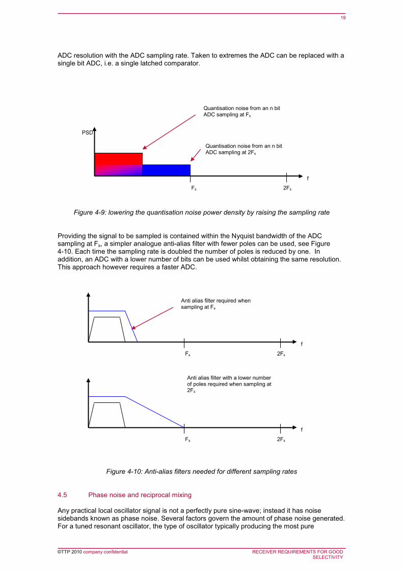
This can lead to many more ADC bits being required than is needed to just decode the signal. For example in a GSM system where the minimum C/N needed is around 9dB and could theoretically be sampled using a two bit ADC, a 10 bit ADC with up to 60dB dynamic range is often used. 4.4.3 ADC oversampling The RMS quantisation noise error level is fixed by the input range and number of bits of the ADC. It is independent of bandwidth and in a simple ADC; the noise energy is spread evenly over the ADC’s Nyquist bandwidth. When the Nyquist bandwidth is made wider by using a higher sample rate, the noise density (watts/Hz) is lower maintaining the same total noise power. Therefore within the desired signal bandwidth, the SQNR is improved. This is shown pictorially in Figure 4-9. By doubling the sample rate it can be seen that the ADC noise density is halved giving a 3dB improvement in dynamic range. This is equivalent to adding an extra half bit to the ADC’s resolution. Using this approach, known as oversampling, the designer can trade
channel power
estimate
A D DSP
LNA input band filter
narrow band loop Wideband loop
wideband power estimate
channel filter
19
©TTP 2010 company confidential RECEIVER REQUIREMENTS FOR GOOD
SELECTIVITY
ADC resolution with the ADC sampling rate. Taken to extremes the ADC can be replaced with a single bit ADC, i.e. a single latched comparator.
Figure 4-9: lowering the quantisation noise power density by raising the sampling rate Providing the signal to be sampled is contained within the Nyquist bandwidth of the ADC sampling at Fs, a simpler analogue anti-alias filter with fewer poles can be used, see Figure 4-10. Each time the sampling rate is doubled the number of poles is reduced by one. In addition, an ADC with a lower number of bits can be used whilst obtaining the same resolution. This approach however requires a faster ADC.
Figure 4-10: Anti-alias filters needed for different sampling rates 4.5 Phase noise and reciprocal mixing Any practical local oscillator signal is not a perfectly pure sine-wave; instead it has noise sidebands known as phase noise. Several factors govern the amount of phase noise generated. For a tuned resonant oscillator, the type of oscillator typically producing the most pure
f
Fs 2Fs
f
Fs 2Fs
Anti alias filter with a lower number of poles required when sampling at 2Fs
Anti alias filter required when sampling at Fs
PSD
f
Fs 2Fs
Quantisation noise from an n bit ADC sampling at Fs
Quantisation noise from an n bit ADC sampling at 2Fs

20
©TTP 2010 company confidential RECEIVER REQUIREMENTS FOR GOOD
SELECTIVITY
waveform; the Q, or quality factor of the resonating tank circuit is an important contributing component to the oscillator phase noise. Several different, but effectively equivalent, definitions of Q exist. One of the most fundamental definitions is for a system under sinusoidal excitement at a frequency ω:
dissipated energy average
stored energyω≡Q
It can be shown that that the 3dB bandwidth of a circuit, BW, resonating at ω0 is related to Q by:
Q
ω=BW 0
The formula shows that the higher the resonator’s loaded Q, the lower the bandwidth of the resonant circuit and therefore the lower the phase noise of the oscillator. Leeson’s formula predicts a tuned resonant oscillator phase noise and is shown in Figure 4-11. Its shape is governed by the following factors:
• Far from the carrier the noise is constant. This represents the broad band noise floor of the oscillator circuit.
• Closer to the carrier the Q of the resonator dictates the noise floor. The 1/f2 response
comes from the filtering action of the resonating tank circuit.
• Close to the carrier, flicker noise with a 1/f characteristic combines with the resonator noise to produce a 1/f3 response. Flicker noise appears in many different physical forms including galactic radiation and transistor noise. In electronics it results from a variety of effects, such as impurities in a conductive channel, and generation and recombination noise in a transistor due to the base current. It is always related to a DC current. The corner frequency fc is the point at which flicker noise becomes more significant than other broad band noise. Different materials have different corner frequencies. Bipolar devices often have corner frequencies of tens or hundreds of Hertz whilst MOS devices have corner frequencies of tens of Kilohertz to Megahertz.
Figure 4-11: Local oscillator phase noise
Log Δω ωc
3c )ω1/(Δ∝
2c )ω1/(Δ∝
~Δω1/f3 ~ω0/2Q
9dB/octave
6dB/octave
= constant

21
©TTP 2010 company confidential RECEIVER REQUIREMENTS FOR GOOD
SELECTIVITY
In practice LO oscillators use a PLL based frequency synthesiser to lock the tuned oscillator to a frequency multiple of a reference oscillator. The synthesiser modifies the noise produced by the tuned oscillator. This will be investigated in section 8.4.2. Figure 4-12 shows the effects of mixing a wanted signal along with a larger adjacent channel signal, both depicted as a pure sine wave, to a lower IF frequency. The local oscillator noise is mixed with both the wanted signal and adjacent channel interferer. The down converted wanted signal is swamped by the adjacent channel signal, now with added phase noise. This effect is known as reciprocal mixing.
Figure 4-12: Reciprocal mixing 4.6 Receiver sensitivity The amount of noise each stage adds is described by its noise figure. Noise factor (F) is the ratio of the total output noise power from a device compared to the output noise due just to the input source. When expressed in Decibels it is known as the Noise Figure (NF). It assumes the source is at 290K (17°C). In a real receiver multiple receiver stages are cascaded together. Each stage develops some noise, and noise developed in one stage is fed through to the next. Therefore the SNR of the received signal degrades with each additional receiver stage. This degradation can be minimised by sufficient amplification of the signal in the prior stage so that the latter stage has little effect on the overall noise.
123
4
12
3
1
21total GGG
1FGG
1FG
1FFF +++=
When each stage of a receiver has sufficient gain, the noise figures of the first elements in the receiver, often an input filter followed by an LNA, have the largest effect on the receiver’s overall noise figure. If this gain is reduced, the back end components noise figure has a much larger effect on the receiver’s noise figure. Receiver sensitivity contributes to receiver selectivity especially when the wanted signal is small. By maximising receiver sensitivity, the SNR of the received signal is maximised allowing greater amounts of interference degradation from the effects of distortion, channel filtering etc before the SINR becomes too small for the receiver to decode the signal adequately.
LO
adjacent channel interferer
wanted signal
down converted wanted signal ‘swamped’ by down converted adjacent channel interferer
IF
Input signals and local oscillator
After down conversion

22
©TTP 2010 company confidential RECEIVER REQUIREMENTS FOR GOOD
SELECTIVITY
4.7 Receiver dynamic range The concept of dynamic range can be used to describe the difference between the maximum signal the receiver can handle and the smallest. As discussed in section 3 the receiver may not need full sensitivity when receiving strong interfering signals. When using an AGC system, the receiver’s gain is adjusted depending on the size of the wanted input signal and possibly also the size of the interferers. If the gain of the stage that dominates the large signal handling of the receiver, characterised by the receivers IP3 or P1dB performance is reduced the overall large signal handling performance of the receiver improves. At the same time, as the receiver gain is reduced, the receiver’s noisy back end components have more effect on the receiver’s overall noise figure causing it to degrade. Generally as the receiver’s gain reduces the receiver’s noise figure increases. The noise figure generally increases more rapidly than the receiver’s IP3 and the receiver’s dynamic range reduces at high signal levels. As an example, Figure 4-13 below shows the P1dB and NF performance of the MAX2371, an LNA with input step attenuator followed by a VGA (Voltage controlled gain amplifier). It is designed to be used at the input to a receiver. A sharp step in the gain can be seen as the front end 20 dB attenuator is switched in. As the gain reduces the noise figure degrades and the P1dB improves slightly. A marked improvement is seen in P1dB as the attenuator is switched in.
-40
-30
-20
-10
0
10
20
30
40
1 2 3 4 5 6 7 8 9 10
front end attenAGC voltagegainP1dBNoise figure
Figure 4-13: LNA with step attenuator and VGA’s P1dB and NF performance with gain
(MAX2371, Maxim Integrated Products) When the amplifier is coupled to the rest of a receiver the front end gain tends to have a larger effect on the overall P1dB, or IP3 of the receiver. The graph below shows the simulated IP3 and noise figure performance of the receiver when the MAX2371 is coupled to a receiver back end with a gain of 10dB, noise figure of 10dB and IP3 of 0dBm. It can be seen that the IP3 varies significantly with the receiver gain. With small input signals, the receiver gain and IP3 of the back end of the receiver dominate whilst at small signals the IP3 of the front end dominates.

23
©TTP 2010 company confidential RECEIVER REQUIREMENTS FOR GOOD
SELECTIVITY
-30
-20
-10
0
10
20
30
40
50
1 2 3 4 5 6 7 8 9 10
front end attenAGC voltagegainIP3Noise figure
Figure 4-14: RX performance with the MAX2371 LNA coupled to a nominal receiver back-end
4.8 Transmit adjacent channel power leakage Although not directly a receiver performance issue, many modulation systems do not constrain all their transmit power to their allocated transmit frequency channel. Any energy transmitted on adjacent channels is known as adjacent channel power leakage, ACPL. If say 1% of the power leaks into the adjacent channels either side of the transmit frequency this will constrain the best ACR obtainable, even with a perfect receiver, to around 23dB. 4.9 Summary Table 4-1 lists the various receiver impairments discussed above and examines the number and type of interferer required to cause a selectivity issue. Impairment Susceptible frequency channels Number and type of interferer
required to cause a selectivity issue
Channel filtering (analogue and digital)
Mostly the adjacent channel with channels further from the wanted having a reduced susceptibility as the analogue filter transitions to its stop band. The ultimate rejection of the filter will influence the far off blocking performance of the receiver.
At least one
Linearity Any frequencies that are not adequately suppressed by an input filter prior to processing by the receivers analogue element, amplifiers, mixers, etc operating non-linearly.
Either one with non constant envelope modulation or two signals. The intermodulation products must fall on the wanted, IF, DC frequency etc (receiver architecture dependent).
Spurious responses Any that are not adequately suppressed prior to processing by the receivers analogue elements, amplifiers, mixers, etc; that combine with the receiver’s LO (and its harmonics) or internally generated spurious frequencies which result in a spurious product being generated that falls on the
At least one

24
©TTP 2010 company confidential RECEIVER REQUIREMENTS FOR GOOD
SELECTIVITY
Impairment Susceptible frequency channels Number and type of interferer required to cause a selectivity issue
wanted, IF, DC frequency (receiver architecture dependent).
ADC aliasing Any frequencies that are not adequately suppressed by the ADC’s alias filter prior to sampling.
At least one with spacing such that interferer is aliased into the ADC’s desired band
LO phase noise – reciprocal mixing
Mostly the adjacent channel with channels further from the wanted have a reduced susceptibility as the LO phase noise levels out. The ultimate LO noise floor of the filter will influence the far off blocking performance of the receiver
At least one
Transmit adjacent channel power leakage
Mostly the adjacent channel with channels further from the “wanted” having a reduced susceptibility as the transmitter output filter transitions to its stop band.
At least one
Table 4-1: Receiver selectivity impairments
From the table it can be seen that, with the exception of receiver linearity, a receivers selectivity can be determined using a single interferer. To comprehensively determine a receiver’s selectivity, potential interferers at any frequency which may be present at the receiver’s input need to be considered. 4.9.1 Typical receiver performance Figure 4-15 shows the selectivity of a typical DTT tuner using a superhet receiver with a SAW IF filter for different received power levels. Both the wanted and interferer have an occupied bandwidth of around 7.6MHz. The frequency offset is the distance between the centre of the wanted and unwanted signals. At relatively low wanted signal levels, -70dBm is likely to be around 10dB above the receiver’s sensitivity limit, the selectivity improves as the frequency separation of the interferer to wanted increases. This is likely to be mostly due to RF front end filter selectivity although local oscillator phase noise causing reciprocal mixing and transmit adjacent channel power leakage may play a part.
Further out some spurious responses can be seen. The clearest is at +72MHz. As it is only on one side of the wanted signal it can be assumed that it is the image response of the receiver. At higher signal levels the reduced dynamic range of the receiver dominates.

25
©TTP 2010 company confidential RECEIVER REQUIREMENTS FOR GOOD
SELECTIVITY
Figure 4-15: Measurements of selectivity (C/I) for DVB-T interference into a DTT receiver for
different received power levels (C) (Ofcom/ERA) .
26
©TTP 2010 company confidential INTERFERENCE EFFECTS ON AND BY
VARIOUS MODULATION TYPES
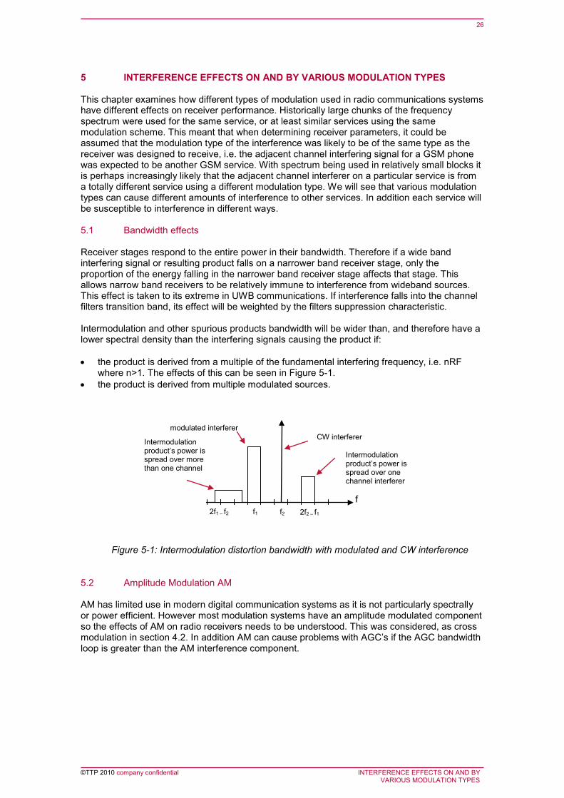
5 INTERFERENCE EFFECTS ON AND BY VARIOUS MODULATION TYPES This chapter examines how different types of modulation used in radio communications systems have different effects on receiver performance. Historically large chunks of the frequency spectrum were used for the same service, or at least similar services using the same modulation scheme. This meant that when determining receiver parameters, it could be assumed that the modulation type of the interference was likely to be of the same type as the receiver was designed to receive, i.e. the adjacent channel interfering signal for a GSM phone was expected to be another GSM service. With spectrum being used in relatively small blocks it is perhaps increasingly likely that the adjacent channel interferer on a particular service is from a totally different service using a different modulation type. We will see that various modulation types can cause different amounts of interference to other services. In addition each service will be susceptible to interference in different ways. 5.1 Bandwidth effects Receiver stages respond to the entire power in their bandwidth. Therefore if a wide band interfering signal or resulting product falls on a narrower band receiver stage, only the proportion of the energy falling in the narrower band receiver stage affects that stage. This allows narrow band receivers to be relatively immune to interference from wideband sources. This effect is taken to its extreme in UWB communications. If interference falls into the channel filters transition band, its effect will be weighted by the filters suppression characteristic. Intermodulation and other spurious products bandwidth will be wider than, and therefore have a lower spectral density than the interfering signals causing the product if: • the product is derived from a multiple of the fundamental interfering frequency, i.e. nRF
where n>1. The effects of this can be seen in Figure 5-1. • the product is derived from multiple modulated sources.
Figure 5-1: Intermodulation distortion bandwidth with modulated and CW interference
5.2 Amplitude Modulation AM AM has limited use in modern digital communication systems as it is not particularly spectrally or power efficient. However most modulation systems have an amplitude modulated component so the effects of AM on radio receivers needs to be understood. This was considered, as cross modulation in section 4.2. In addition AM can cause problems with AGC’s if the AGC bandwidth loop is greater than the AM interference component.
f2 f1 2f2 – f1 2f1 – f2 f
CW interferer modulated interferer
Intermodulation product’s power is spread over more than one channel
Intermodulation product’s power is spread over one channel interferer

27
©TTP 2010 company confidential INTERFERENCE EFFECTS ON AND BY
VARIOUS MODULATION TYPES
5.3 Frequency modulation FM FM, and its digital equivalent, Continuous Phase Frequency Shift Keying (CPFSK) is a constant envelope analogue modulation system (Figure 5-2) and therefore can cope with non linear amplification without producing intermodulation products. This allows fairly power efficient amplifiers to be used and simple receivers to be constructed, two of the principle reasons why FM is widely used for radio broadcasting and in first generation cellular systems. The modulation bandwidth is dependent on the bandwidth of the baseband and the frequency deviation away from the carrier. However, especially when a wide deviation is used this does not result in a well bandwidth constrained signal limiting the adjacent channel performance obtainable. In an analogue FM system constraining the RF bandwidth, results in baseband distortion. Excessive filtering of the signal after modulation, in a digital system will result in inter-symbol interference. 5.4 GMSK as used in GSM Minimum shift keying, MSK, can be considered as either a type of phase shift keying (PSK) or a continuous phase frequency shift keyed signal with some of the desirable properties of both classes of modulation. The PSK nature of the signal makes MSK fairly efficient allowing the signal to be decoded at low C/No. The CPFSK constant envelope nature of the signal allows the signal to be non-linearly amplified. This allows power efficient amplifiers to be used in the transmitter and no spectral re-growth to occur within the receiver if a receiver stage mildly distorts the signal.
Figure 5-2: Constant and non constant envelope power The FSK nature of the modulation does however mean the signal is not well spectrally constrained. To improve this, a Gaussian filter is applied to the baseband signal before modulation. This makes the system significantly more spectrally efficient. However as the frequency channels are packed very close together, with a spacing of 200KHz, there is still very significant ACPL resulting in the GSM specification only requiring an adjacent channel selectivity of 9dB4
GSM uses time division multiple access to allow several users to simultaneously use a frequency channel. Transmitted signals using this time division approach are modulated in bursts. This causes the signal to have a large AM component which can cause significantly more interference than a CW signal. Many types of electronics can act as a signal detector to
. Little power leaks into the alternate channel allowing an alternate channel selectivity of 41dB to be specified. The poor ACPL needs to be managed for continuous blocks of GSM through network design. Guard bands are needed each side of GSM spectrum to protect other services from its interference.
4 ETSI, TS 145 005, V8.4.0 “Digital cellular telecommunications system (Phase 2+); Radio transmission and reception (3GPP TS45.005 version 8.4.0 release 8)”
OQPSK modulation constellation diagram
GMSK modulation constellation diagram showing constant envelope power
Q Q
I I
28
©TTP 2010 company confidential INTERFERENCE EFFECTS ON AND BY
VARIOUS MODULATION TYPES
signals such as GSM even if the detected signals are at a significantly higher frequency than what the electronics is designed to operate at. A typical example of this interference is the “t…d…t…d…t….t…d” noise heard on a standard PSTN phone when a GSM phone rings nearby. If an AM signal is detected by any second-order distortion in the receiver, the AGC loop is likely to have a step response. This results in the dynamic range of the receiver being reduced. Most cellular systems capacity to carry voice or data traffic is limited by interference. Typically this is co-channel interference. To minimise this interference the transmit power is limited to be just sufficient for the call to take place thereby limiting the likelihood of both co-channel and adjacent channel interference. In a real world cellular environment, due to the user moving and multipath, the transmit power required to just make the call is constantly changing. In many systems, including GSM a different frequency is used for the uplink (from mobile to base-station) and downlink (from base-station to mobile). As the multipath is very frequency dependent the transmit power for each link will be constantly changing independently of each other. To allow an appropriate transmit power to be used, a feedback system needs to be incorporated into the transmissions to allow the receiver to report back to the transmitter if it needs to change it’s transmit power. GSM does incorporate this feedback but it is inefficient often resulting in more transmit power being used than necessary thereby creating more interference. 5.5 WCDMA WCDMA (Wideband code division multiple access) is a form of direct sequence spread spectrum. Two types of WCDMA have been defined within the 3rd Generation Partnership Project (3GPP). FDD needs paired spectrum, i.e. separate channels for uplink and downlink whilst TDD can operate in unpaired spectrum. FDD is most commonly used and is discussed in this section. WCDMA uses an orthogonal complex QPSK signal for the uplink and a QPSK signal for the downlink. The orthogonal complex QPSK modulation reduces the peak to average ratio of the signal to be transmitted allowing a reasonably power efficient amplifier to be used. Data symbols are root raised cosine filtered to minimise their frequency bandwidth without introducing inter symbol interference. A code is added to the data signal to be transmitted allowing code division multiple access (CDMA) to be used. The code allows the receiver to separate out the wanted signal from other signals multiplexed on the same carrier. This coding also has the effect of widening the bandwidth of the signal making it more robust to narrowband fading. In order for CDMA to work well the base station needs to receive all the signals with equal power. This requires very good power control resulting in lower average transmit power. WCDMA’s ACPL is reasonably good and the channels do not overlap allowing WCDMA channels to operate next to each other. This allows a receiver adjacent channel selectivity of 33dB5
In the receiver, spectral re-growth of received interferer close to the wanted signal will result in additional interference being generated in the wanted channel degrading the C/N0 of the received signal, i.e. the receivers selectivity is degraded. Low level distortion will mostly cause
to be specified. Steps have been taken to minimise any regular repetitive power bursts in the transmissions limiting the TDD interference noise. QPSK is used for the WCDMA downlink. As QPSK is not constant envelope, any non-linearities in the transmitter or receiver circuitry cause out of channel cross modulation products. When linked to a digitally modulated carrier this phenomenon is often known as spectral re-growth. This re-growth must be controlled in the transmitter in order for the transmitter to meet is regulatory defined transmission mask.
5 ETSI, TS 125 101, V8.6.0 “Universal Mobile Telecommunications System (UMTS); User Equipment (UE) radio transmission and reception (FDD) (3GPP TS 25.101 version 8.6.0 release 8)

29
©TTP 2010 company confidential INTERFERENCE EFFECTS ON AND BY
VARIOUS MODULATION TYPES
3rd order products in the adjacent channel as shown in Figure 5-3. Higher level distortion will cause 5th order distortion in the adjacent and alternate channels as shown in Figure 5-4.
Figure 5-3: WCDMA signal with 3rd order distortion
Figure 5-4 WCDMA signal with 5th order distortion
The shape and level of the distortion can be estimated if the linearity IP parameters of the receiver are known6
Due to limited TX to RX isolation of the duplexer the transmitted signal will leak into the receiver. This creates what is possibly the strongest interferer to the received signal. In addition, as there is always one tone present, only one, rather than two, interferer signals are needed to cause multitone intermodulation problems. This contributes to needing a receiver with a reasonably
. WCDMA uses FDD where, unlike GSM, the mobile’s transmitter and receiver are operating at the same time. To avoid the transmitter causing interference directly at the receive frequency needs a transmit signal with low noise in the receive band. This requires a transmit LO with low wideband phase noise and a well filtered baseband.
6 Wu, Qiang; Xiao, Heng; Li, Fu; Dec 1998, “Linear RF Power Amplifier Design for CDMA Signals: A Spectrum Analysis Approach”, Microwave Journal
WCDMA input signal
f
WCDMA output signal Power (dBm)
WCDMA input signal
f
WCDMA output signal Power (dBm)

30
©TTP 2010 company confidential INTERFERENCE EFFECTS ON AND BY
VARIOUS MODULATION TYPES
good IP2 and IP3 performance. The IP3 needed is around -15dBm7
5.6 OFDM
whilst the IP2 is more receiver architecture specific. In addition the receiver LO must have a good wideband phase noise to avoid the transmit signal being reciprocally mixed into the wanted receive channel.
OFDM, orthogonal frequency division multiplexing is used in a wide range of broadcast, wireless networking and cellular systems including:
• DAB digital radio broadcast • DVB-T digital terrestrial TV broadcast • IEEE802.11 (Wi-Fi) wireless networking • WiMax • LTE, long term evolution of cellular (4G)
OFDM signals consist of multiple carriers closely spaced in frequency. Each carrier is individually modulated at a low data rate using typically QPSK or higher level QAM. The carriers spacing and the modulation rate of the carriers is set such that they don’t interfere with each other using the mathematical property of orthogonality. This approach also means that there are fairly sharp, well defined edges to the spectrum prior to amplification. A typical theoretical spectrum is shown in Figure 5-5. 2K and 8K refers to the number of OFDM carriers used, 2048 and 8192 respectively.
Figure 5-5: OFDM spectrum (ETSI)8
Each OFDM carrier is individually modulated. The instantaneous power depends on the data modulating each of the carriers, which is typically random and therefore can change widely resulting in a signal with a high peak to average ratio. Distortion products from these carriers will be created when the signal is non-linearly amplified causing spectral re-growth similar to that discussed in section
5.5. This process is sometimes called intra-modulation rather than intermodulation as all the signals are coming from the one source.
7 Liu, Chris W; Damgaard, Morten; May 12th 2009. “IP2 and IP3 Non linearity Specifications for 3G/WCDMA receivers”, Broadcom Corporation available from http://www.mwjournal.com/BGDownload/Broadcom_IP2_IP3_.pdf [accessed 24 July 2009] 8 ETSI EN300 744 “Digital Video Broadcasting(DVB); Framing structure, channel coding and modulation for digital terrestrial television”

31
©TTP 2010 company confidential INTERFERENCE EFFECTS ON AND BY
VARIOUS MODULATION TYPES
As OFDM has a high peak to average ratio it is susceptible to spectral re growth. At the transmitter a number of techniques are used to minimise these effects. These include:
• Limiting or even clipping the signal prior to amplification. Care needs to be taken to not distort the signal too much causing a high modulation error (MER).
• Pre-distortion. The signal is distorted with the inverse of the anticipated amplifier non linearities so that the amplified signal is as close to the wanted signal as possible.
• Sharp filtering after the power amplifier. These filters are large and expensive as they need to have a very high Q, low power loss and acceptable group delay at the band edges. These filters are typically used in broadcast transmitters where the transmit powers are often very high. They allow the broadcast to be constrained within a tight spectral mask whilst still using a reasonably efficient amplifier. These filters are not applicable, using current technology, to low cost consumer type equipment.
At the receiver these techniques are generally not applicable. Instead the receiver needs to be designed with sufficient linearity. The actual receiver intermodulation performance required cannot be predicted quite as neatly as it is possible for WCDMA as it depends on the modulation of each carrier. However, typically 15 to 20dB higher IP points than what would be required for CW signals at the same power are needed.9
Orthogonality of the multiple carriers used in OFDM allows efficient demodulator implementations using the FFT algorithm. Whilst frequency selective, each FFT point or bin has a sin x/x response. This causes some leakage of energy from one FFT frequency bin into the others and vice versa. This results in an average out of band rejection noise floor of around 25dB.This is illustrated in
Figure 5-6.
Figure 5-6: Receiver chain with OFDM demodulation 9 Behzad, A; 2008. “Wireless LAN Radios, System Definition to Transistor Design”, IEEE Press, page 89.
frequency
Single FFT noise bin
OFDM interfering signal
Signal power (dB)
Cumulative ACI power per OFDM carrier
OFDM carrier
Adjacent Channel interference FFT noise floor
-5
-35
-25
-15
Accumulation of all FFT bin energy sets a noise floor

32
©TTP 2010 company confidential INTERFERENCE EFFECTS ON AND BY
VARIOUS MODULATION TYPES
In general OFDM signals are reasonably tolerant to narrow band interferers. Assuming the narrow band interferer is sufficiently small to allow the wanted signal to be sampled with sufficient SNR, the narrow band interferer will only affect the C/N of the OFDM carriers it interferes with. OFDM carriers away from the interferer will not be affected. 5.6.1 DVB-T, DAB DVB-T and DAB digital radio both use OFDM. OFDM was partially selected due to the good frequency efficiency of OFDM with the ability to use a Single Frequency Network to provide broadcast coverage of very large areas using multiple transmitters all transmitting simultaneously in the same frequency channel. Selectivity issues associated with SFN’s were discussed in section 1. In DAB differential QPSK modulation is used giving simple synchronisation and good mobile performance. DVB-T, typically optimised for static reception in a Ricean channel, uses up to 64QAM giving very good spectral efficiency. Channels are spaced fairly closely together with a small guard band between them. In DAB an occupied bandwidth of 1.514MHz is used with a guard band of 176KHz. In 8MHz channel DVB-T, an occupied bandwidth of around 7.6MHz is used with a guard band of 800KHz between channels. Transmit powers used for broadcast are much higher than those used for cellular and other devices, enabling good coverage of wide areas with relatively few transmitters. The C/N0 ratios needed to receive OFDM based DVB-T or DAB are significantly lower than the analogue modulation schemes they replaced. Analogue transmitters with EIRPs of up to around 1MW were used. Post digital switch over transmit powers will be limited to the 10 to 200KW range. The standard EN50248:2001, “Characteristics of DAB Receivers” specifies a minimum ACR of 30dB for DAB receivers. Many of the early DAB tuners were based on adaptations of TV tuners and obtained an Adjacent Channel Rejection (ACR) of around 40dB. Later receivers have been based on single chip silicon tuners. Whilst using far less power, enabling battery powered devices; these tuners often have a typical ACR of 35dB and sometimes barely exceed the minimum performance of 30dB. Alternate channels and interference from other channels is not formerly specified except for a far off interferer specification of 40dB with an FM interferer. The DVB-T Bluebook specifies a minimum ACR of 29dB for DVB-T receivers with interferer levels specified for alternate through to the 4th channel away from the wanted. A two tone linearity test is also specified with unwanted carriers two and four channels from the wanted. These tests can be passed with a receiver with an IP3 of around -5 to -10dBm. 5.6.2 LTE LTE, Long Term Evolution, is designed to allow evolution of the current 3G standards such as UMTS to the 4th generation standards. LTE was ratified by ETSI in 2008, with many major cellular operators such as Verizon anticipating first deployments in 2010. LTE will use an OFDMA downlink with a SC-FDMA uplink. This allows the handset to use an OFDM receiver but still use a reasonably power efficient transmitter. New features includes the use of MIMO and flexible RF bandwidths. Receiver RF parameters are similar to those specified for UMTS.
33
©TTP 2010 company confidential RECEIVER ARCHITECTURES
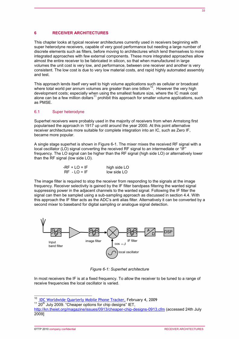
6 RECEIVER ARCHITECTURES This chapter looks at typical receiver architectures currently used in receivers beginning with super heterodyne receivers, capable of very good performance but needing a large number of discrete elements such as filters, before moving to architectures which lend themselves to more integrated approaches with few external components. These more integrated approaches allow almost the entire receiver to be fabricated in silicon, so that when manufactured in large volumes the unit cost is very low, and performance, between one receiver and another is very consistent. The low cost is due to very low material costs, and rapid highly automated assembly and test. This approach lends itself very well to high volume applications such as cellular or broadcast where total world per annum volumes are greater than one billion10. However the very high development costs; especially when using the smallest feature size, where the IC mask cost alone can be a few million dollars11
6.1 Super heterodyne
prohibit this approach for smaller volume applications, such as PMSE.
Superhet receivers were probably used in the majority of receivers from when Armstong first popularised the approach in 1917 up until around the year 2000. At this point alternative receiver architectures more suitable for complete integration into an IC, such as Zero IF, became more popular. A single stage superhet is shown in Figure 6-1. The mixer mixes the received RF signal with a local oscillator (LO) signal converting the received RF signal to an intermediate or “IF” frequency. The LO signal can be higher than the RF signal (high side LO) or alternatively lower than the RF signal (low side LO). -RF + LO = IF high side LO RF - LO = IF low side LO The image filter is required to stop the receiver from responding to the signals at the image frequency. Receiver selectivity is gained by the IF filter bandpass filtering the wanted signal suppressing power in the adjacent channels to the wanted signal. Following the IF filter the signal can then be sampled using a sub-sampling approach as discussed in section 4.4. With this approach the IF filter acts as the ADC’s anti alias filter. Alternatively it can be converted by a second mixer to baseband for digital sampling or analogue signal detection.
Figure 6-1: Superhet architecture In most receivers the IF is at a fixed frequency. To allow the receiver to be tuned to a range of receive frequencies the local oscillator is varied.
10 IDC Worldwide Quarterly Mobile Phone Tracker, February 4, 2009 11 20th July 2009. “Cheaper options for chip designs” IET, http://kn.theiet.org/magazine/issues/0913/cheaper-chip-designs-0913.cfm (accessed 24th July 2009]
A D DSP
cos ωct
local oscillator
image filter IF filter
Input band filter

34
©TTP 2010 company confidential RECEIVER ARCHITECTURES
6.1.1 IF filter The IF filter is generally at a lower fixed frequency than the received RF signal allowing a high Q filter to be implemented to provide the required selectivity. The ideal IF filter, shown in Figure 6-2, should have a flat pass band and good group delay to pass the wanted frequency channel without distortion; with very steep skirts on both sides of the pass band in order to be able to reject the adjacent channels well.
Figure 6-2: Ideal filter response
Filter insertion loss in the pass band is not critical as long as an appropriate amount of amplification can be applied prior to the filter without the amplification introducing too much distortion. Typical adjacent channel rejection which can be obtained with an IF filter range from 30dB up to at least 90dB. For instance a typical crystal filter used in 12.5KHz channelized PMR systems may have a pass band of 7.5KHz at 21.4MHz and an out of band rejection of 90dB, 8.75KHz away. The filter must have very good frequency tolerance and stability over temperature so that it always filters the correct channel. In order to ensure that the wanted channel is always passed when all tolerances are taken into account, the filter may need to be made with a wider pass band than the frequency channel which is to be received. This will cause the receiver’s adjacent channel rejection to be degraded. Tolerance errors can arise from both the IF filter and local oscillator frequency accuracy. The receiver’s ability to reject the alternate and other channels further from the wanted frequency channel is influenced by how quickly the filter transitions from its pass band to its stop band and it’s ultimate out of band rejection. A number of typically passive technologies are used to realise IF filters including crystals, ceramic, and SAW filters. As these filters tend to be available for a range of system standard IF frequencies including 455KHz - AM, 10.7MHz – FM broadcast and 36MHz – TV. Due to the high Q’s and high stability at high frequencies required, the IF filter is rarely integrated into an IC. 6.1.2 Image filter Assuming a low side local oscillator is used, where the local oscillator is at a lower frequency than the wanted receive frequency, i.e. the wanted frequency is at ωc+ωif; then the input band filter and image filter together must reject the receiver’s image response at ωc-ωif. For a high side local oscillator the opposite is true, the wanted frequency is at ωc-ωif and the receiver’s image response is at ωc+ωif. Assuming the amplifiers and mixer prior to the IF filter have the same response to ωc+ωif and ωc-ωif all the image rejection needs to be provided by the combined response of the input band and
Pass band one channel wide
Ideally infinitely steep filter skirts
Good out of band rejection with no spurious responses at high and low frequencies
IF Adjacent Alternate Adjacent Alternate
f
Amplitude response (dB)

35
©TTP 2010 company confidential RECEIVER ARCHITECTURES
image filters. These filters need to operate directly at the RF frequency so high Q’s are required. Any filter placed directly at the input of receiver will directly affect, and may dominate, the receiver’s noise figure and therefore the receiver’s sensitivity to receive weak signals. The input band filter must therefore have low insertion loss. The insertion loss of the filter following the LNA is less critical. However the LNA must have adequate linearity to not distort any signals passed by the input band filter. Assuming a fixed frequency IF is used and the receiver is designed to receive a range of frequencies the image filter must have adequate image rejection. The selectivity required can range from 40dB for DAB to at least 70dB in PMR systems. This must be obtained irrespective of what frequency the local oscillator is tuned to. One approach is to use a fixed frequency image filter as shown in Figure 6-3. With this approach the pass-band of the filter needs to be as wide as the tuning range of the receiver. At the same time the filter needs to be able to reject the image frequency when the receiver is tuned to the highest wanted frequency. As the tuning range of the receiver increases, the lowest received frequency and the highest image frequency get closer together making it more difficult to get adequate rejection until eventually the lowest wanted frequency and highest image overlap. At this point it becomes impossible to realise the image filter using this approach. This example uses a low side LO although a high side LO can equally be used.
Figure 6-3: Filter pass band required with a fixed frequency image filter Image filters can be made from various different materials, largely depending on the frequency of operation and the pass bandwidth required. At lower frequencies wire wound inductors and ceramic capacitors are often used whilst for instance for cellular physically small SAW filters etched on a variety of substrates are used. As the image to wanted frequency separation is 2 x ωif; the need to separate the wanted and image frequencies can be helped by choosing a higher IF frequency. This approach can be extended so that the IF frequency is actually above the RF filter. This allows a low Q image filter to be used but makes realising a narrow band channel filter at the high IF frequency very difficult. Often with this approach a wider bandwidth IF filter is used at the high frequency and a second heterodyne stage is then used to mix the signal to a lower frequency where the channel filtering can be done. With this approach care needs to be taken to ensure all the receiver prior to the channel filter is suitably linear and that any secondary images formed in the additional mixing stages are suitably filtered. Cable modems which need to receive signals over the very wide band from around 108MHz to 862MHz often use this approach. Another approach is to use a much narrower filter which has a tuneable pass-band. It is generally more complicated to build a tuneable filter. However assuming the filter can “track” the receive frequency it does allow a receiver with a wide tuning range to be developed.
0
Image frequency range (ωc-ωif)
ωif
PSD
ω
Local oscillator range
wanted frequency range (ωc+ωif)
Image filter pass-band. It must pass the lowest wanted frequency
The image filter must have adequate rejection to reject the highest image frequency
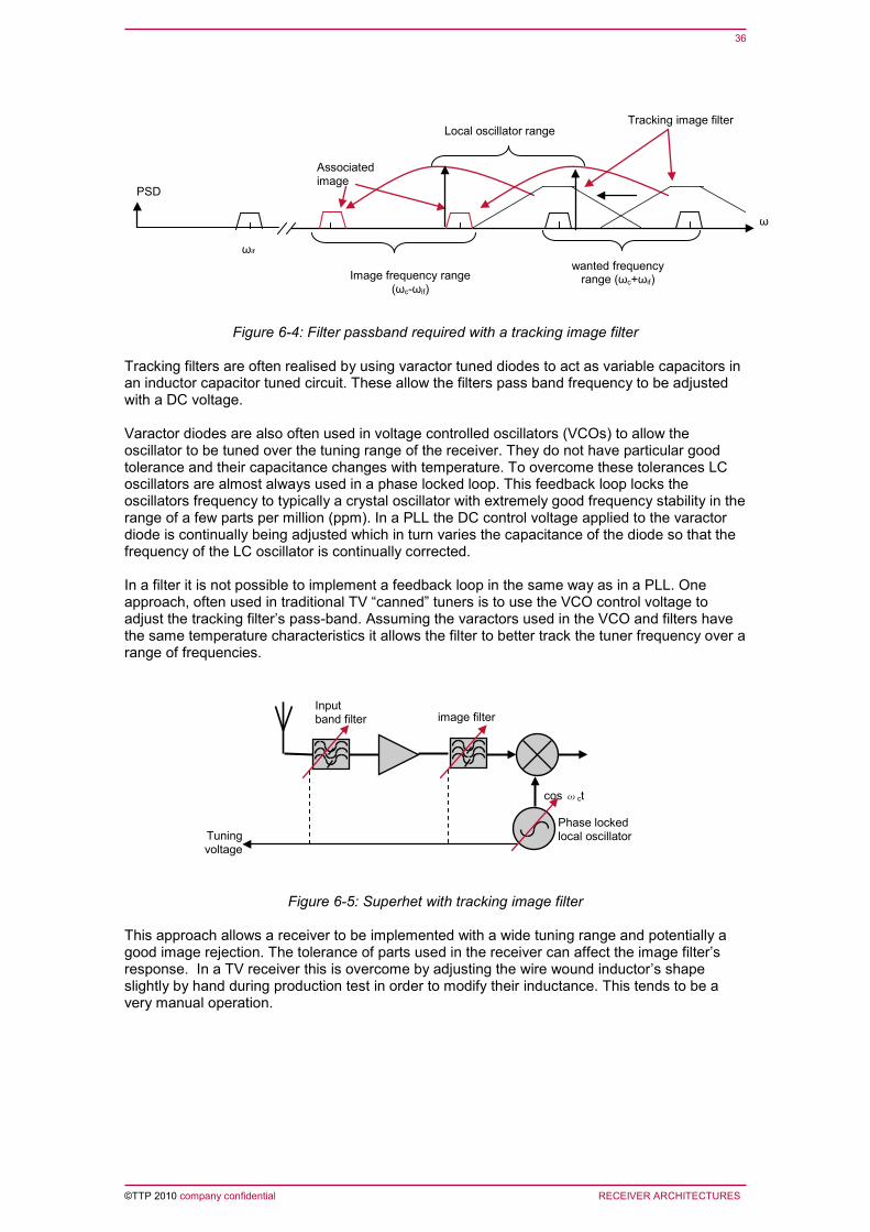
36
©TTP 2010 company confidential RECEIVER ARCHITECTURES
Figure 6-4: Filter passband required with a tracking image filter Tracking filters are often realised by using varactor tuned diodes to act as variable capacitors in an inductor capacitor tuned circuit. These allow the filters pass band frequency to be adjusted with a DC voltage. Varactor diodes are also often used in voltage controlled oscillators (VCOs) to allow the oscillator to be tuned over the tuning range of the receiver. They do not have particular good tolerance and their capacitance changes with temperature. To overcome these tolerances LC oscillators are almost always used in a phase locked loop. This feedback loop locks the oscillators frequency to typically a crystal oscillator with extremely good frequency stability in the range of a few parts per million (ppm). In a PLL the DC control voltage applied to the varactor diode is continually being adjusted which in turn varies the capacitance of the diode so that the frequency of the LC oscillator is continually corrected. In a filter it is not possible to implement a feedback loop in the same way as in a PLL. One approach, often used in traditional TV “canned” tuners is to use the VCO control voltage to adjust the tracking filter’s pass-band. Assuming the varactors used in the VCO and filters have the same temperature characteristics it allows the filter to better track the tuner frequency over a range of frequencies.
Figure 6-5: Superhet with tracking image filter This approach allows a receiver to be implemented with a wide tuning range and potentially a good image rejection. The tolerance of parts used in the receiver can affect the image filter’s response. In a TV receiver this is overcome by adjusting the wire wound inductor’s shape slightly by hand during production test in order to modify their inductance. This tends to be a very manual operation.
cos ωct
Phase locked local oscillator
image filter
Input band filter
Tuning voltage
Associated image
Image frequency range (ωc-ωif)
ωif
PSD
ω
Local oscillator range
wanted frequency range (ωc+ωif)
Tracking image filter

37
©TTP 2010 company confidential RECEIVER ARCHITECTURES
6.1.3 Mixer spurious responses As well as an image response, super heterodyne receivers are susceptible to interferers at other spurious frequencies. One particular well known 2nd-order spurious response, called the half-IF spurious response, occurs at 2fRF-2fLO for a low side local oscillator. An interferer at fLO+1/2fIF will cause the response, i.e. when: 2f(RF-1/2IF) – 2fLO = fIF = fRF - fLO
Figure 6-6: Location of half IF spurious frequency
A similar response falls at f(RF+1/2IF) for a high side LO. To guard against the ½ IF response, a combination of two mitigation approaches can be used. These are to:
1. Use a mixer with very good rejection of 2fRF-2fLO. The degree of rejection can be predicted by the mixers IP2 response.
2. Filtering of the input signal prior to mixing reduces any signals at f(RF-1/2IF) which could cause a spurious signal from reaching the mixer.
To filter the ½ IF response, the filter needs to have some rejection closer to the filter’s pass band than is needed for image rejection. This results in a narrower band filter being required prior to mixing, than is needed just for image rejection. This places more constraints on using, in a receiver with a wide tuning bandwidth, a fixed frequency image filter than those discussed in section 6.1.2 above. Another mixer spurious response is due to leakage, or feed-through, of energy between mixer ports. Mixers ideally convert all their input RF energy to the IF frequency. In practice, due to imperfect isolation between mixer ports, some RF and IF energy will leak through to the IF causing a spurious response. 6.1.4 Image reject mixers The superhet receiver discussed so far use the amplitude response of filters to reject the image frequency. Another approach is to use mixers operating in quadrature to cancel out the image signal. Two architectures are often used to realise this approach, Hartley and Weaver. For both the Weaver and Hartley image reject mixer, it is necessary to generate signals in quadrature to each other. For perfect image rejection these quadrature signals need to be phase and gain matched across the frequency band of interest. 6.1.4.i Hartley The Hartley image rejection architecture is shown in Figure 6-7. The RF signal is down converted by quadrature LO signals. The resulting IF signals are then low pass filtered and after one is phase shifted by 90° the IF signals are combined. This result is that, depending on which channel is subjected to the 90° phase shift, either the image or wanted channel being rejected.
f(RF-1/2IF) fIF FLO fRF

38
©TTP 2010 company confidential RECEIVER ARCHITECTURES
Figure 6-7: Hartley image reject architecture
The image rejection obtainable is dependent on how close to 90°the phase shift of the local oscillator is, how similar are the amplitude responses of the two arms of the mixer and how close to 90° is the final phase shift. The image rejection ratio (IRR) of the image reject mixer can be described as a function of any phase and/or amplitude imbalance as: IRR = ¼ x [(ΔA/A)2 + θ2] where ΔA/A = relative gain mismatch θ = relative phase mismatch in radians. It can be shown that an amplitude mismatch of 0.1dB and a phase mismatch of 1° yields around 41dB of IRR. To realise this degree of IRR requires careful design and possibly some form of calibration. Without calibration the IRR often drops to 25dB, equivalent to an amplitude imbalance of 0.5 to 0.75dB and a phase mismatch of 3 to 5°. Rather than splitting the LO into quadrature, a similar result can be obtained by splitting the RF into quadrature and using a single LO. Whilst mathematically it may give the same result, in practice it is easier to split the high, constant level LO signal with good amplitude and phase match rather than split into quadrature the small varying RF signal. 6.1.4.ii Weaver The Weaver image rejection architecture is shown in Figure 6-7.
0 90°
0°
90°
Σ RF input IF output sin ωct
cos ωct

39
©TTP 2010 company confidential RECEIVER ARCHITECTURES
Figure 6-8: Weaver image reject architecture The Weaver approach overcomes the amplitude mismatch issues caused by needing to add a 90°phase shift to one arm of the quadrature mixer by adding a second pair of mixers to realise the phase shift. This second mix does create another set of image frequencies which need to be addressed. One approach is to use a second IF centred on DC (0Hz) with the sampling of the signal being done in quadrature as shown in Figure 6-9.
Figure 6-9: Quadrature Weaver architecture
0 90
Σ
RF input
I
sin ωc1t
sin ωc2t
cos ωc2t
cos ωc1t
sin ωc2t
Σ
Q
0 90
Σ RF input IF output
0 90
sin ωc1t sin ωc2t
cos ωc2t cos ωc1t

40
©TTP 2010 company confidential RECEIVER ARCHITECTURES
6.2 Zero IF receiver A zero IF receiver overcomes the IF image response issue by directly converting the signal to baseband centred around 0Hz using two mixers operating in quadrature. Its architecture is shown in Figure 6-10.
Figure 6-10: Direct conversion receiver With the LO at the RF frequency the down converted image signal falls directly on the wanted signal. Both the wanted and image signals are mirror images of each other reflected around the frequency axis.
Figure 6-11: Zero IF image down conversion with image suppression The image signal suppression depends on the amplitude and phase matching of the quadrature mixer as defined for the image reject mixer in section 6.1.4.i. The image suppression combined with factors such as the receiver noise figure and ADC quantisation noise level define the receiver’s noise floor and hence sensitivity. Inadequate image suppression causes distortion as the reflected image of the wanted signal falls directly on the down converted wanted signal. This helps define the maximum C/NO that can be obtained from the receiver.
0 90
A D
A D
DSP
I
Q
DC offset control
Complex LO RF signals
f
f
0
0
Baseband signals suppressed sideband
RF signals

41
©TTP 2010 company confidential RECEIVER ARCHITECTURES
Whilst the zero IF approach deals with the image response, the receiver still has significant spurious responses at odd LO harmonics, i.e. 3fLO, 5fLO, 7fLO…. In a zero IF receiver, as the local oscillator is at the RF frequency, any received signals at these frequencies will cause interference. In narrow band receivers, where frequencies at 3fRF etc do not need to be received, fixed frequencies input filters can be used. In very wide band receivers, such as cable TV receivers needing to cover 48 to 860MHz, this can be a significant problem. The analogue low pass filters following the mixer help provide the receivers selectivity and act as anti-alias filters to the ADC. If all the selectivity is provided by these filters, they can have a cut off frequency at half the channel bandwidth and must reject the adjacent channel and other channels further from the wanted frequency by the selectivity required. As the low pass filters operate at a low frequency they can be implemented with active analogue filters. These filters do need good amplitude matching to obtain the required image rejection as discussed in 6.1.4.i. These active filter stages often have limited dynamic range compared to the passive IF filters typically used in superhets. This is often because the filter stages have a finite ultimate far off rejection. To overcome this limitation the filters are often broken into a number of stages and inserted between programmable gain amplifier stages as shown in Figure 6-12 with each amplifiers gain programmable. This allows an AGC system to be implemented. This filter-amplifier approach is very applicable to integration into the receiver IC. Gain matching, for example, within an IC can be controlled better than trying to achieve good matching across a number of discrete elements.
Figure 6-12: Distributed gain and filtering Usually some of the receiver’s selectivity requirement is realised with digital filters following the ADC. Digital filters don’t suffer from many of the limitations of analogue filters such as their performance being affected by component and silicon process tolerances, cross talk and noise. This allows their performance to be closely defined and very repeatable. In addition they can be implemented in low cost ‘digital CMOS’ making use of either DSP processors or custom digital circuitry. With this approach the ADC must have enough bits of resolution to sample any high level adjacent and other channels without clipping, whilst not degrading the low level wanted signal with quantisation noise. Whilst the zero IF approach appears to minimise the image issue, the architecture does introduce other issues. These issues are mainly centred on needing a lot of amplifier gain to amplify signals near or at DC. These include:
• Second order receiver linearity • Local oscillator leakage and DC offsets • DC offsets • Flicker noise
In section 4.2 receiver linearity was discussed. In superhet receivers third order distortion is most critical. The IP3 of all elements prior to the channel selection filter contribute to the overall
Maximum signal

42
©TTP 2010 company confidential RECEIVER ARCHITECTURES
receiver IP3. The overall worst case IP3 can be determined by summing the distortion products of each stage, created near the received frequency taking into account how much each of these distortion products have been amplified by the receiver. Once third order products are generated which fall into the channel the receiver is tuned to, they cannot be filtered out. The IP3 of the mixer is often the most significant element in the receiver chain. In zero-IF receivers the second order spurious product generated at DC falls directly onto the down converted wanted frequency corrupting the wanted signal and potentially saturating the receiver. The receiver therefore needs to have a high second order intercept point. As the LNA is AC coupled to the mixer, its IP2 tends to not need to be considered as this can be filtered out by AC coupling the LNA to the mixer. The mixer and subsequent baseband amplifier and filter stages are usually DC coupled. Therefore the IP2 of both the mixer and subsequent stages do need to be very good. For example, to cope with interference from the handset’s transmitter, an IIP2 of +48dBm is typically needed for UMTS12, and to cope with a GSM adjacent channel interferer, 40dBm is needed for GSM13
Any local oscillator signal, which is at the same frequency as the received signal, leaking into the input of the mixer could be mixed down to DC causing a DC offset similar to that generated by second order distortion within the mixer itself.. Potential paths for this interference are shown in
. Differential circuits are almost essential as their symmetry reduces even order distortion.
Figure 6-13. In a superhet receiver the LO signal is at a different frequency to the received signal and is usually attenuated by the receiver’s image filter, however in a Zero IF receiver the LO signal as at the same frequency as the received signal. This can be a significant issue. Any LO signal that leaks out through the LNA to the antenna will be re-radiated, potentially causing interference to other users.
Figure 6-13: LO leakage paths Potential paths for LO leakage in a direct conversion receiver includes:
1. From the LO into the RF port of the mixer causing a constant level DC offset. 2. From the LO into the input of the LNA. The LNA will then amplify the signal causing a
greater DC offset. The level of the offset will depend on the gain of the amplifier. 3. If a portion of a large received interferer leaks into the local oscillator the interferer will
then mix with itself causing a varying level offset. 4. The LO leaking out through the LNA. This will directly cause interference to other
devices and to the receiver itself if the signal reflects off external surfaces and is re- received.
Leakage paths 1 and 2 are continuous and therefore create a time invariant amount of DC offset. Leakage path 3 depends on the level of the interfering signal which will vary over time. The level of any signal reflected back into the receiver having leaked out via leakage path 4 will also vary with time depending on the positioning of the receiver and if the receiver is being used
12 Chris W. Liu, Morten Damgaard, Broadcom Corporation “IP2 and IP3 Nonlinearity Specifications for 3G/WCDMA Receivers” Microwave Journal http://www.mwjournal.com/BGDownload/Broadcom_IP2_IP3_.pdf [28th July 2009] 13 http://www.commsdesign.com/design_corner/showArticle.jhtml?articleID=16504800 [28th July 2009]
4
3
2
1
Local oscillator Input
band filter

43
©TTP 2010 company confidential RECEIVER ARCHITECTURES
in a moving environment. Time invariant amounts of DC offset are easier to handle than varying amounts of DC offset. DC offsets due to leakage can be minimised through good RF matching and layout by reducing asymmetries in the design. Balanced circuitry is almost universally used. DC offsets can also be caused by imbalances in the amplifiers and analogue circuitry itself, for example op-amp offset voltages. Although DC offsets can be minimised by good RF layout, careful choice of baseband amplifiers etc, it is usually still necessary to actively compensate for them. Compensation methods can include:
• AC coupling, or high pass filtering of the signal following the mixer. This will cause a ‘hole’ in the centre of the pass band potentially causing some corruption of the signal. This corruption can be minimised by positioning the corner frequency of the high pass filter as close to DC as possible. However too low a corner frequency will result in a slow transient response. This may be required to cope with AGC gain or input level changes. AC coupling can be used with UMTS but is not applicable to the bursty TDD signals used in GSM. OFDM systems, such as Wi-Fi14
omit the central carrier for this purpose.
• Cancelling out most or all of the DC offset using compensation. Circuits for AC coupling and compensation methods will be discussed further in section 8.6.3.iii below. As most of the receiver gain is at baseband, 1/f or flicker noise contributes to the noise floor of the receiver degrading device sensitivity. MOS devices, used in many low cost modern RF ICs have a high 1/f corner frequency, typically of a few MHz, making this a significant problem. It is found that for a given gm, the larger the MOSFET, the lower the 1/f noise. However larger MOSFETs take more silicon area and silicon area is closely connected to device cost. Wider band systems, such as UMTS and DVB-T, are less affected by flicker noise than narrow band system, such as GSM, as a greater portion of their bandwidth is likely to be above the 1/f corner frequency. To reduce the design sensitivity to 1/f noise, the receiver must have sufficient gain at RF so that the noise floor of the latter stages has less significance. 6.3 Low IF receiver References 15
Using a low IF frequency allows the IF channel filter to be integrated into silicon.
A low IF receiver attempts to overcome the DC offset and 1/f noise issues associated with zero IF receivers whilst still using an approach that lends itself to a high degree of integration. Many radio standards require less selectivity for interfering signals occurring in adjacent channels than they do for interfering signals in other channels. Low IF receivers often make use of this by choosing an IF frequency which makes the image frequency fall into an adjacent channel.
Figure 6-14 shows where the adjacent, alternate channels and image response are down converted to when a low side local oscillator is used positioned on the edge of the wanted frequency channel in the receivers adjacent channel fall into the receive channel and signals in the alternate channel fall into the receiver adjacent channel. It can be seen that the receiver must achieve sufficient image rejection to meet the required adjacent channel specification. In addition, it can be seen that the lower alternate channel, after
14 Behzad, Arya; 2008.”Wireless LAN Radios System Definition to Transistor Design” IEEE Press, page 58 15 Gu, Qizheng; 2005. “RF System design of Transceivers for Wireless Communications” Springer

44
©TTP 2010 company confidential RECEIVER ARCHITECTURES
down conversion, lies next to the wanted frequency. Any adjacent channel leakage power (ACPL) from the lower alternate channel originally transmitted on the high side of the transmission, after down-conversion will fall into the wanted channel. This energy cannot be suppressed by filtering after down conversion and therefore the receiver must have sufficient image rejection to adequately suppress the signal. It is found in systems such as GSM with poor ACPL performance, that ACPL sets the image rejection requirements in a low IF receiver.
Figure 6-14: Low IF down-conversion
As the image is so close to the wanted frequency, an image filter at the receiver input can’t be used, however image reject techniques can be used. One approach is by using the dual quadrature mixer Weaver architecture as shown in Figure 6-15. The second set of mixers are implemented digitally, and the second digital LO is set so that the output is centred around DC.
Alternate Alternate LO Adjacent Adjacent
Wanted frequency
Image frequency f
Alternate DC Adjacent
wanted
Input signal
Image down converted to the wanted frequency
│f│
Alternate channel down converted to the adjacent channel
After down conversion

45
©TTP 2010 company confidential RECEIVER ARCHITECTURES
Figure 6-15: Digital low IF Weaver architecture The signals are down converted to a low IF frequency by the first set of mixers. The I and Q signals are low pass (anti alias) filtered and sampled. As discussed in section 6.1.4, due to phase and gain errors between each arm of an analogue image reject mixer, it is very difficult to achieve greater than 40dB of image rejection. 25 to 35dB is commonly achieved without calibration. By using digitally implemented amplifiers, mixers and summers much better image rejection can be achieved. As an example, the TI CC1021 IC, designed to receive the 880 and 915MHz ISM bands, achieves an image rejection of typically 25dB with no calibration. This increases to typically 50dB with calibration. One calibration approach is discussed below. With in line amplifiers gain α set to one and cross coupled amplifier’s gain β set to zero any analogue phase and gain errors from the first mixers propagate through the system. By adjusting the gains of α and β it can be shown that these phase and amplitude errors can be significantly reduced. It is possible, by adjusting the output summers to the signs shown in brackets and injecting a CW test tone into the inputs of the mixer during a calibration mode, to determine the values of α and β. With α and β determined, when the output summers are reset to their normal settings the analogue offsets errors are calibrated out. A polyphase band pass filter can be used instead of digital down conversion to obtain reasonable image rejection. The RC circuit approach shown in Figure 8-7 can be extended to give a reasonable amplitude match over a wider frequency range. For example, by staggering the two RC time constants each side of the centre frequency, the circuit shown in Figure 6-16 has a gain consistent to 0.2dB over roughly a 20% bandwidth. A significant disadvantage though is that it has significant attenuation and therefore is susceptible to noise. Further stages could be added to further broaden the useful bandwidth.
0 90
II
QI
A
D α
β DSP
II
IQ
QI
DLO_I
DLO_I
DLO_Q
ID
I(IM)
QD
Q(IM)
A D
LPF
LPF
+
+
-
-

46
©TTP 2010 company confidential RECEIVER ARCHITECTURES
Figure 6-16: Two stage broadband quadrature generator Whilst a high-pass filter has a symmetrical notch at DC, the response of a Hilbert filter, obtained by shifting the high-pass filter response along the frequency axis, is not mirrored about zero frequency (Figure 6-17).
Figure 6-17: Hilbert Filter The type of circuit shown in Figure 6-16 provides a Hilbert response and is known as a polyphase filter. The key attribute of the filter is that it provides a different filter response for positive and negative frequencies unlike most filters which just respond to the absolute frequency of the signal and not the sign of the signal. Using this approach an ‘image reject’ filter
C1
C1
C1
C1
C2
C2
C2
C2
R1
R1
R1
R1
R2
R2
R2
R2
Iin
Iin_b
Qin
Qin_b
Iout
Iout_b
Qout_b
Qout
0 ω
Hilbert filter
-ω0 0
Highpass filter
ω
ωC ωC

47
©TTP 2010 company confidential RECEIVER ARCHITECTURES
can be built. For a single stage filter a zero is found at 1/RC thereby forming a bandstop filter as shown in Figure 6-18.
Figure 6-18: Ideal response of a single stage polyphase image reject filter
Multiple stages can be cascaded together to allow good rejection across a wide bandwidth. In practice the on chip RC time constant may vary from lot to lot so calibration of the filters corner frequencies is required. Alternatively the bandwidth of the filter must be sufficient to overcome these tolerances. For good image rejection each RC section of the filter must be well matched. To reject the image by 60dB with a 3σyield, the filter’s resistors and capacitors must match to a σ of 0.094% assuming Gaussian distribution. As the variance of on-chip capacitors and resistors is proportional to the inverse of their surface area large die areas are required16
Figure 6-19
. The passive stages can also be combined with op-amps to help overcome the attenuation and noise limitations of a fully passive approach. These amplifiers need to be matched as accurately as the polyphase filter components.
shows an image reject polyphase filter integrated with a quadrature mixer to implement a low IF receiver. Whilst this approach shows the polyphase filter which rejects the image frequency it does not show the channel filter. The channel filter may be implemented in the analogue domain prior to the ADC. Alternatively it may be implemented digitally. In either case there needs top sufficient filtering prior to the ADC to avoid aliasing issues.
16 Behbahani, Farbod et al, 2001, “CMOS Mixers and Polyphase Filters for large image rejection”, IEE Journal of Solid-State Circuits, Vol 36, No 6 June 2001
1/RC ω
response to positive frequency
response to negative frequency

48
©TTP 2010 company confidential RECEIVER ARCHITECTURES
Figure 6-19: Low IF receiver with polyphase filter Phase and amplitude variations in the quadrature mixer and imbalances in the polyphase filter all contribute to limiting receiver’s image rejection. By using a double quadrature mixer, rather than the single quadrature mixer discussed previously, where both the RF and LO are split into quadrature it can be shown that the image rejection only depends to a second order on the quadrature inaccuracy in the LO and RF. For instance to reject an image by 60dB in a single quadrature mixer requires 0.1% of phase match whilst in the double quadrature mixer only 3% phase matching is required. A double quadrature mixer is shown in Figure 6-20.
Figure 6-20: Double quadrature mixer
0 90
polyphase filter
A D
A D
DSP
I
Q
0 90
RFI
RFQ
cos(ωLOt)
cos(ωLOt)
sin(ωLOt)
sin(ωLOt)
IFI
IFQ

49
©TTP 2010 company confidential RECEIVER ARCHITECTURES
In some designs, e.g. many DAB receivers, where only a single ADC is available in the baseband IC, the I and Q signals after filtering are connected to a quadrature modulator and converted to another slightly higher IF frequency for sampling by a single ADC17
6.4 Architecture comparison
. Whilst low IF receiver overcome many of the problems associated with zero IF receivers such as DC offsets, flicker noise and second order distortion they do require twice as wide a channel filter, wider dynamic range and twice the minimum sampling rate compared to a zero IF receiver. The higher frequency channel filter implies more poles are needed. All these factors lead to greater current consumption.
Table 6-1 summarises the selectivity limitations of the various receiver architectures discussed.
17 Luff, Gwilliam et al, 2006. “A Compact triple band T-DMB/DAB RF Tuner with an FM Receiver”, IET Seminar on RF for DVB-H/DMB Mobile broadcast, London

50
©TTP 2010 company confidential RECEIVER ARCHITECTURES
Superhet Low IF Zero IF Sensitivity LNA, flicker noise not
important LNA, flicker noise may be important
LNA, flicker noise more important
Image rejection
Image filter and image reject mixer rejection. Enough image rejection needed for adequate selectivity at the image frequency, typical tens of MHz away from the wanted
Phase and amplitude matching of mixers plus: • Digital approach -
enough ADC dynamic range and bandwidth for digital dual down convertor
• Analogue approach - polyphase filter rejection
Enough image rejection needed for adequate C/N and selectivity at frequencies close to the wanted ACPL from the alternate channel mixes into the wanted signal and may dictate the image rejection required
Not a selectivity issue Enough image rejection needed for adequate C/N for signal decoding
Spurious response rejection
Limited by: • Input filter rejection • Mixer mFRF±nFLO
response • Mixer RF to IF and LO
to IF isolation It is likely all the spurious frequencies will be in frequency channels well away from the wanted channel and therefore may be subject to interfering signals much higher than the higher than the wanted signal
Limited by: • Input filter rejection • Mixer mFRF±nFLO
response • Mixer RF to IF and LO
to IF isolation A number of the most significant spurious frequencies due to factors such as the mixers ½ IF response will be in the wanted or adjacent frequency channels and therefore not subject to interfering signals higher than the adjacent channel signal
Limited by: • Input filter rejection • Mixer mFRF±nFLO
response • Mixer RF to IF and LO
to IF isolation A number of the most significant spurious frequencies due to factors such as the mixers ½ IF response will be in the wanted frequency channel and therefore not subject to signals higher than the wanted signal
Channel filtering
Limited by: • Discrete filter + ADC
dynamic range • LO phase noise External high Q filters needed
Digital approach limited by: • ADC dynamic range • mixer image rejection • LO phase noise Analogue approach limited by: • Integrated analogue
filter • mixer image rejection • polyphase filter rejection • LO phase noise Medium Q filters needed, either integrated analogue filters or digital
Limited by: • integrated analogue
filter • ADC dynamic range • LO phase noise Lowest Q filters needed, either integrated analogue filters or digital
Linearity IP3 important, IP2 not so important
IP3 and IP2 important IP2 critical
Table 6-1: Receiver architecture selectivity limitations

51
©TTP 2010 company confidential RECEIVER ARCHITECTURES
Key points from this table are:
• The superhets image filter can be eliminated in the zero IF and low IF architectures. However in a superhet, an image filter whilst also acting as an input RF filter can provide very significant spurious response rejection, channel filtering and enhanced linearity for interfering signals several channels away from the wanted frequency. A superhet’s adjacent channel filtering is provided by a discrete fixed filter with potentially very high Q and post ADC digital filtering
• A Low IF receiver’s adjacent and alternate channel selectivity is provided by a
combination of the receiver’s image rejection and channel filtering. Selectivity of one of the adjacent channels is provided solely by the receiver’s image rejection. Minimal input filtering will limit receiver selectivity and linearity for interfering signals several channels away from the wanted.
• Zero IF receivers adjacent channel selectivity is provided by the receiver’s integrated
analogue and digital filtering. Zero IF receivers performance can be limited by even order linearity. Minimal input filtering will limit receiver selectivity and linearity for interfering signals several channels away from the wanted.

52
©TTP 2010 company confidential SILICON PROCESSES
7 SILICON PROCESSES Lower cost is the prime motivation for using CMOS over BiCMOS and III-V materials (e.g. GaAs, GaN etc.). As an example CMOS NFETs can achieve the same high frequency performance as SiGe BiCMOS HBT (Heterojunction Bipolar Transistor) at roughly half the feature size (i.e. a 130nm BiCMOS HBT has comparable high frequency performance to a 65nm NFET) and hence a quarter of the silicon area. Many of the processing costs in IC manufacture are area related so minimising area is a way of reducing manufacturing cost. In general for stand alone RF circuits, where surface area is dominated by passive devices and I/O pads BiCMOS offers the lowest cost option despite an additional 20% increase in processing complexity18
As lithographic dimensions shrink in advanced CMOS nodes, new process technologies need to be developed to maintain and improve on the key RF device parameters. With each new node the design rules get more complicated and mask sets more expensive. For instance the mask set data size needed to make an IC is expected to double every four years and currently stands, for an advanced CMOS process, at around 655GB per layer
. However when small amounts of digital logic is to be integrated into the system, CMOS has a clear advantage as transistor density and chip size scale with the square of the minimum lithographic dimension. Scaling improvements give benefits in terms of conserving battery power, increasing frequency performance and increasing integration. Traditional CMOS device scaling requires increased channel doping to maintain performance. However an assumption of the scaling formulae is that the ability of electric fields to move carriers in the channel (the mobility coefficient) remains constant. This is not always true. Beyond doping concentrations of 1016cm-3, the mobility of silicon falls off sharply. Smaller geometries result in higher parasitic impedances and increased process variations. Also smaller film thicknesses and shorter gate lengths result in higher leakage currents and drain conductance. These issues are in part compensated for by a lower supply voltage, however this increases sensitivity to process variation and reduces voltage headroom & thus potentially receiver dynamic range.
19
• Higher transconductance (gm)
. The number of transistors an RF designer can handle is increasing at a much slower rate so the development cost of an IC using the most advanced processes is increasing. Although production costs are reduced by using these process nodes, increasingly the rising development cost of an RF IC means that these nodes can only be justified for the highest volume products such as cellular, Bluetooth, Wi-fi and possibly TV tuners. Bipolar transistors, particularly SiGe HBTs implemented in BiCMOS have dominated the market in chip designs for wireless applications and have been historically preferred over FET devices due to higher performance device characteristics including:
• Higher voltage tolerance
• Lower flicker noise (1/f noise)
• Current-voltage relationships that are more easily modelled with analytic expressions
However FETs have several advantages over bipolar transistors. The turn-on (or threshold) voltage of bipolar transistors is determined by the semiconductor band gap whereas for FETs the threshold voltage (Vt) is adjustable with doping levels. Also comparing a 130nm SiGe HBT and a 90nm CMOS NFET for an application where fT = 100GHz, a 3x reduction in power dissipation can be achieved with an RF CMOS NFET. 18 Thomas H. Lee, 2004, “The Design of CMOS Radio Frequency Integrated Circuits”, 2nd Edition, Cambridge University Press 19 ITRS, 2007, “Lithography”, International Technology Roadmap for Semiconductors, 2007 Edition http://www.itrs.net/Links/2007ITRS/2007_Chapters/2007_Lithography.pdf [17th August 2009]

53
©TTP 2010 company confidential SILICON PROCESSES
7.1 RF NFET Key Device Parameters The sections below identify the key design parameters for an RF NFET device, and how these are affected as lithographic dimensions shrink. In addition various technologies are discussed to maintain / improve on RF parameter performance. 7.1.1 Self gain Self gain is defined as gm/gDS (Transconductance / drain (or output) conductance), where transconductance is the ability of the device to source the current and the output conductance tells us how well that current is sourced with swings in the output voltage. Good self gain is required for good large signal handling. For CMOS FETs self gain reduces with the reduction in gate size primarily due to:
• The reduction in gate oxide thickness • An increase in DIBL (Drain Induced Barrier Lowering)
In the FET channel velocity saturation limit, Transconductance (gm) scales with the inverse of gate oxide thickness (1/tox), as shown in the following equation:
OX
SATm t
VWg ε=
Thus as tOX reduces, the value gm (transconductance) tends to increase which is desirable; however for devices with small lithographic dimensions, gDS (output conductance) is related to DIBL due to the high electric field at the source of the FET during high drain bias. Thus gDS will increase as VDS/LGATE increases (High source voltage and small gate length). Since VDS does not scale as fast as the gate length the net result is that gDS increases, resulting in a net reduction in self gain gm/gDS. In addition beyond 90nm the gate leakage restricts the scaling of the oxide layer (tOX) so that LGATE and tOX cannot be reduced proportionately further restricting an increase in gm. To counteract these ‘short channel effects’ outlined above, for gate sizes ~65nm asymmetric ‘Halo’ implants can be used to reduce gDS thus improving self gain. To reduce gate leakage and maintain gate oxide (tox) scaling a combination technology of utilizing high-k dielectrics along with metal gates can be used. Conventionally silicon dioxide has been used as a gate oxide insulator material. However with a drive to smaller dimensions, thicknesses below 2nm this results in leakage currents due to the dramatic increase in electron tunnelling (electron leakage through the thin oxide layer). This leads to unwieldy power consumption and reduced device reliability. Replacing the silicon dioxide gate dielectric with a high-K- material reduces these leakage effects.
Unfortunately high-K materials are generally not compatible with polysilicon gate electrode structures due to high threshold voltages and degraded channel mobility (lower gm) resulting in poor drive current performance. Metal gates in combination with high-k dielectrics can provide the correct transistor threshold voltages, alleviate the mobility degradation problem and reduce gate dielectric leakage. This technology will become particularly important for gate nodes of 45nm or less. Thus high-k dielectrics and metal gate electrodes are required to enable continued equivalent gate oxide thickness scaling, thus reducing gate oxide leakage, which ultimately results in self gain being maintained for smaller technology nodes
Double Gate (DG) and Ultra Thin Body (UTB) gate structures can also be used to reduce the short channel effect by again reducing the effect of gate current leakage through electron tunnelling, and controlling the gate threshold characteristics so that it is neither too high nor too low (which also facilitates good inter-device matching). Based on estimates of off state drain

54
©TTP 2010 company confidential SILICON PROCESSES
leakage currents these advanced device structures could be saleable down to an ultimate limit of 10nm gate length. In summary self gain can be severely limited within CMOS FET structures down to smaller lithographic nodes due to a reduction in the gate oxide thickness and DIBL. The implementation of technologies such as asymmetric Halo implants, high-K materials, metal gates and DG / UTB gate structures serve to:
• Reduce gate dielectric leakage by ensuring continued gate oxide thickness scaling
• Control gate threshold values within required limits
• Alleviate electron mobility degradation and thus maintaining gm
7.1.2 fT, fmax fT and fmax are commonly used by manufacturers as a figure of merit for the performance of their devices - these parameters are defined below:
• fT is the gain bandwidth frequency of the device; it is the frequency at which the short circuit gain approximates unity (i.e. cut-off frequency).
• Fmax is the maximum frequency of oscillation, it is the frequency at which the maximum
available power gain of the transistor is equal to 1 (i.e. maximum frequency of oscillation)
With shrinking node size, the lateral and vertical scaling leads to lower parasitics and thus to faster speeds for CMOS devices. By using transistors with good fT and fmax analogue signal processing and linearising techniques such as negative feed back can be used at higher frequencies improving the large signal handling of the circuit. Both fT and fmax are dependent upon the gate structure - fmax will have a peak value at some optimum gate width above which it is limited by physical gate resistance and below which it is limited by parasitic losses in the FET structure. For a given layout, the optimum device width shrinks as the unit gate resistance increases with smaller and smaller gate lengths. Care must be taken in the FET layout to minimise parasitic gate capacitance that will limit FT and gate resistance that will limit fmax and noise figure. Thus fmax has the potential to increase with technology scaling whilst maintaining optimum gate width and resistance ratios. However this is particularly difficult to achieve in practice despite the increase in fT due to the increasing impact of the parasitics in the device layout. 7.1.3 Noise figure The noise figure (NF) of a device depends on its intrinsic properties including its internal capacitances and transconductance gm. The overall noise figure of a FET is dominated by two components:
• The thermal noise of the channel
• Resistance of the gate The scaling behaviour of the channel thermal noise is dominated by that of gdo/gm
2 (where gdo is the channel conductance at zero drain-source bias) and thus the noise performance should therefore improve with successive technology nodes (as transconductance increases with smaller node size). Noise figures of 0.56dB have been reported for 250nm geometry and 0.12dB reported for 50nm devices20
20 Iniewski, Krzysztof; 2008. “Wireless Technologies, Circuits, Systems, and Devices” CRC Press, page 307
.

55
©TTP 2010 company confidential SILICON PROCESSES
The noise contribution associated with the gate resistance is highly layout dependent and may be minimised by dividing the overall gate width into a large number of short gate fingers (again the optimum width scales with node size). A well-optimised layout that minimises via and contact resistance contributions including the resistance along the gate polysilicon can reduce the relative contribution of gate resistance to the total drain current noise to less than 10%. Additional improvements can be achieved with the use of metal gates by further reducing the gate resistance. The SOI (Silicon-On-Insulator) process technology available in CMOS can be used to isolate the device from the bulk substrate material in an attempt to reduce noise coupling to and from the device. SOI is discussed in more detail in section 7.2. 7.1.4 1/f or Flicker noise 1/f noise has an amplitude inversely proportional to frequency, and is usually the dominant noise source at low frequencies. The 1/f corner frequency is the frequency above which the noise amplitude is approximately flat and independent of frequency. As it is a low frequency phenomenon it has a direct impact on receiver system components, in primarily the following areas:
• Close to carrier phase noise of a VCO (Voltage Controlled Oscillator)
• Baseband noise in Zero IF receiver architectures In the case of VCOs any low frequency noise will appear as noise sidebands of the oscillator’s output signal. Mixing or subsequent signal processing in other stages can also shift low frequency noise to the centre of the carrier frequency, potentially causing jitter, as well as interfering with adjacent channels and lowering the final SNR. FETs are surface conduction devices where the current flow is affected by the properties of the Si/SiO2 interface. The quality of the p/n junction and the quality of the oxide interface dictate the power of the 1/f noise. 1/f noise appears in the drain current and arises from fluctuations in the number of channel charge carriers as these carriers are captured and released at random by traps located near the oxide / silicon interface. The magnitude of this noise is determined by the density of these traps, the density of channel charge, and the overall gate area as described by the following equation:
OXGATE
mtd CWL
gMf
S 2
21 ⋅
=
As tOX decreases with technology generation, both gm and COX (gate oxide capacitance) increase proportionately. Thus devices of fixed gate width (W) and length (L) should experience no change in 1/f noise, assuming that trap density (Std) can be kept constant. However, if LGATE is scaled to minimum dimensions 1/f noise will increase even without a change in trap density due to both the decrease in LGATE and well as the consequent increase in gm0. Thus as generation to generation scaling in FETs moves oxide interfaces even closer to the active channel, 1/f noise performance is likely to degrade. For a MOS device, the 1/f corner frequency can be between a few tens of kilohertz to more than a megahertz21
7.1.5 RF CMOS device parameter summary
.
Table 4-1 below identifies the important RF parameters for an NFET in the CMOS process, and how the various parameters change in relation to reductions in node size: 21 Thomas H. Lee, 2004, “The Design of CMOS Radio Frequency Integrated Circuits”, 2nd Edition, Cambridge University Press
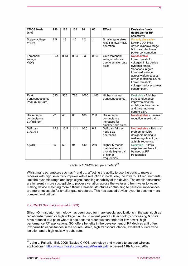
56
©TTP 2010 company confidential SILICON PROCESSES
CMOS Node (nm)
250 180 130 90 65 Effect Desirable / not-desirable for RF selectivity
Supply voltage VDD (V)
2.5 1.8 1.5 1.2 1 Smaller gate sizes result in lower VDD operation.
Partially desirable -Lower VDD limits device dynamic range but does offer lower power consumption.
Threshold voltage VT(V)
0.44 0.43 0.34 0.36 0.24 Gate threshold voltage reduces due to smaller gate sizes.
Not desirable – Lower threshold voltages limits device dynamic range. Variations in gate threshold voltage across wafers causes device matching issues Lower threshold voltages reduces power consumption.
Peak transconductance Peak gm (uS/um)
335 500 720 1060 1400 Higher channel transconductance.
Desirable - A higher transconductance improves electron mobility in the channel and thus improves current gain.
Drain output conductance gDS
a(uS/um)
22 40 65 100 230 Drain output conductance increases for smaller node sizes.
Not desirable - Causes reduction in self gain .
Self gain gm/gDS(-)
15.2 12.5 11.1 10.6 6.1 Self gain falls as node size decreases.
Not-desirable - This is a problem for LNA designers hoping to realise significant gain at high frequency.
fT(GHz) 35 53 94 140 210 Higher fT means that device can provide higher gain at higher frequencies.
Desirable –Allows negative feedback to be used at RF frequencies
Table 7-1: CMOS RF parameters22
7.2 CMOS Silicon-On-Insulator (SOI)
Whilst many parameters such as fT and gm, affecting the ability to use the parts to make a receiver with high selectivity improve with a reduction in node size, the lower VDD requirements limit the dynamic range and large signal handling capability of the device. The smaller structures are inherently more susceptible to process variation across the wafer and from wafer to waver making device matching more difficult. Parasitic structures contributing to parasitic impedances are more noticeable for smaller gate structures. This has caused device layout to become more complex and critical.
Silicon-On-Insulator technology has been used for many special applications in the past such as radiation-hardened or high voltage circuits. In recent years SOI technology processing & costs have reduced to a point where it has become a serious contender for low power, high performance RF applications. SOI offers benefits in the development of RF devices at it offers low parasitic capacitances in the source / drain, high transconductance, excellent buried oxide isolation and a high resistivity substrate. 22 John J. Pekarik, IBM, 2006 “Scaled CMOS technology and models to support wireless applications” http://www.cmoset.com/uploads/Pekarik.pdf [accessed 11th August 2009]
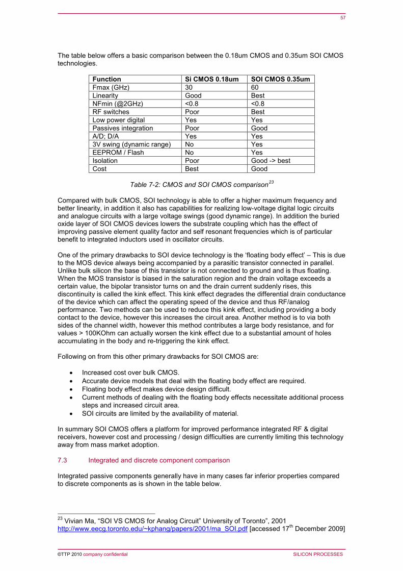
57
©TTP 2010 company confidential SILICON PROCESSES
The table below offers a basic comparison between the 0.18um CMOS and 0.35um SOI CMOS technologies.
Function Si CMOS 0.18um SOI CMOS 0.35um Fmax (GHz) 30 60 Linearity Good Best NFmin (@2GHz) <0.8 <0.8 RF switches Poor Best Low power digital Yes Yes Passives integration Poor Good A/D; D/A Yes Yes 3V swing (dynamic range) No Yes EEPROM / Flash No Yes Isolation Poor Good -> best Cost Best Good
Table 7-2: CMOS and SOI CMOS comparison23
• Increased cost over bulk CMOS.
Compared with bulk CMOS, SOI technology is able to offer a higher maximum frequency and better linearity, in addition it also has capabilities for realizing low-voltage digital logic circuits and analogue circuits with a large voltage swings (good dynamic range). In addition the buried oxide layer of SOI CMOS devices lowers the substrate coupling which has the effect of improving passive element quality factor and self resonant frequencies which is of particular benefit to integrated inductors used in oscillator circuits. One of the primary drawbacks to SOI device technology is the ‘floating body effect’ – This is due to the MOS device always being accompanied by a parasitic transistor connected in parallel. Unlike bulk silicon the base of this transistor is not connected to ground and is thus floating. When the MOS transistor is biased in the saturation region and the drain voltage exceeds a certain value, the bipolar transistor turns on and the drain current suddenly rises, this discontinuity is called the kink effect. This kink effect degrades the differential drain conductance of the device which can affect the operating speed of the device and thus RF/analog performance. Two methods can be used to reduce this kink effect, including providing a body contact to the device, however this increases the circuit area. Another method is to via both sides of the channel width, however this method contributes a large body resistance, and for values > 100KOhm can actually worsen the kink effect due to a substantial amount of holes accumulating in the body and re-triggering the kink effect. Following on from this other primary drawbacks for SOI CMOS are:
• Accurate device models that deal with the floating body effect are required. • Floating body effect makes device design difficult. • Current methods of dealing with the floating body effects necessitate additional process
steps and increased circuit area. • SOI circuits are limited by the availability of material.
In summary SOI CMOS offers a platform for improved performance integrated RF & digital receivers, however cost and processing / design difficulties are currently limiting this technology away from mass market adoption. 7.3 Integrated and discrete component comparison Integrated passive components generally have in many cases far inferior properties compared to discrete components as is shown in the table below.
23 Vivian Ma, “SOI VS CMOS for Analog Circuit” University of Toronto”, 2001 http://www.eecg.toronto.edu/~kphang/papers/2001/ma_SOI.pdf [accessed 17th December 2009]

58
©TTP 2010 company confidential SILICON PROCESSES
Device Parameter Discrete Integrated Resistor Value range 0R to 10M+
(surface mount 0402 , 1 x 0.5mm)
1–10 Ohms per square, polysilicon 1 – 10kOhm per square, well
Tolerance ±1% is standard Typ ±35% Temperature coefficient 100ppm Typ 1000ppm/°C
Capacitor Value range 0.1pF to >1uF (surface mount 0402 , 1 x 0.5mm)
1 – 30 fFum-2
Tolerance ±5% typ ±30% typ Q >1000 Low ~50
Inductor Value range 1nH to 270nH, (surface mount 0402 , 1 x 0.5mm)
1 – 10nH
Tolerance ±2% typ Q 35@1GHz Low ~8@1GHz
Table 7-3 Discrete and Integrated device comparison24
24 Thomas H. Lee, 2004, “The Design of CMOS Radio Frequency Integrated Circuits”, 2nd Edition, Cambridge University Press
To overcome the physical limitations of passive components very different design techniques and circuit topologies are used in comparison to designs utilising a larger number of discrete components. This includes using active rather than passive bias circuits and current mode rather than voltage mode designs. Whilst tolerances are poor, the parameter matching between components on the same die may be better than the parameter matching between discrete components. This opens up many design techniques which rely on the similarity of components parameters rather than the absolute value of the parameters. Unlike active elements, integrated passive elements do not in general scale with the semiconductor process used. Although integrated passive components have severe limitations, they form an essential element in modern RF design allowing physically very small, extremely complex multiband, multi-standard RF receivers to be manufactured at low cost. By using a highly integrated approach the amount of time consuming and expensive RF design and development which needs to be done for an individual product design can be significantly reduced. As well as reducing product development cost, an integrated approach increases the certainty of the timescales needed to bring a new design to market. This is often critical in meeting consumer orientated deadlines such as Christmas.
59
©TTP 2010 company confidential KEY COMPONENTS
8 KEY COMPONENTS This chapter investigates the performance of both discrete and integrated circuit components used in receivers. 8.1 Band select filter 8.1.1 SAW filters Surface Acoustic Wave (SAW) filter technology is utilised for frequencies of up to 3GHz. Fundamentally a SAW filter is a piezoelectric material that converts an incoming electromagnetic signal into an acoustic signal, and vice versa. In its most basic form, the SAW filter consists of a polished piezoelectric substrate with a deposit of two transducers consisting of interdigital arrays (IDT – InterDigital Transducers) of thin electrodes. These interleaved metal electrodes are used to launch and receive the RF waves, so that an electrical signal is converted to an acoustic wave and then back to an electrical signal again. A basic advantage is that acoustic waves travel very slowly (typically 3000 m/s), so that large delays are obtainable The overall frequency response characteristics of a SAW filter are determined by deriving impulse responses for each of the two transducers. These transforms are added together in dB. The surface of a piezoelectric substrate is then etched with the two impulse responses The advantages of SAW filters include:
• Compact packages especially at >100MHz • Low shape factor • Good linear phase characteristics • Good rejection qualities • Relatively stable performance over temperature
Many other advantages are derived from the physical structure of SAW Filters which facilitates robust and reliable designs that remain stable within the application. Additionally, the inherent design and wafer processing techniques of SAW filters provide for a repeatable device in both low and high volume production. The key parameters for a SAW filter are identified and described briefly below:
• Centre Frequency (Fo) This can range from few tens of MHz, where SAW devices are typically used as IF filters, through to several GHz, where they are used as RF input filters.
• Passband Width (Bp) The passband width will pass a signal occupying a specific
frequency band, and reject others falling outside the band. From a SAW filter design perspective, the first parameter to consider is the fractional bandwidth (Bp/Fo) because of the influence on the substrate material to be used in the design. The substrate material influences many parameters; however the most important is the temperature stability specification.
• Transition Bandwidth (Bt). This is the area between the Stop Band and the Passband
found on both sides of the Passband.
• Rejection (REJ.) All ranges of the SAW Filter not including the Passband. The Rejection can also be referred to as the Rejection Range, or Stop Band. We can refer to this as the range in which the relative attenuation is larger than the specified rejection side. With proper material selection and design, Rejection of 50dB, or greater, is possible within a wide selection of fractional bandwidths and shape factors.
• Insertion Loss (IL) The minimum attainable Insertion Loss is generally influenced by the
Fractional Bandwidth and the influences of this ratio on the applicable substrate material. The Insertion Loss value will generally increase when approaching the

60
©TTP 2010 company confidential KEY COMPONENTS
fractional bandwidth limit of a substrate material. Front end SAW filters for the cellular bands generally have an insertion loss of less than 3dB.
The SAW filter substrate must be made of an anisotropic (i.e. it has different properties in each direction) piezoelectric material. This usually means that a crystalline material must be used. Substrate materials include:
• Quartz • Lithium neobate • Lithium tantalate
Because the SAW material is anisotropic, the SAW properties depend on the orientation at which the substrate has been cut from the original material. In general standard orientations are used which are known to give good SAW properties. SAW performance is largely dependent on the choice of substrate material. Quartz for example has weak piezoelectricity, which limits the fractional bandwidth to around 4%. On the other hand it does have excellent temperature stability~10ppm frequency stability over a +/-20C range; Lithium Niobate is the opposite, giving larger bandwidths ~20% but poorer temperature stability. The third material noted above Lithium tantalite is intermediate in both respects. The operating frequency limit is currently limited by fabrication techniques. In production the narrowest line width possible is around 0.3um with the i-line (365nm) UV photolithography typically used in the industry. This corresponds to a quarter wavelength, thus giving the maximum frequency of operation of 3GHz. Various filter topologies are possible. These are achieved by modification of the IDTs, three primary types are available, including IIDT (Inter-digiated Inter-Digital Transducer), DMS (Double Mode SAW), and Ladder type SAW filters. A comparison between the performances of each of these SAW filter topologies is made for RF SAW filters in the table below: Loss Attenuation Bandwidth Power
durability IP3 Balanced
type IIDT 3-4dB 25-50dB Variable Good ~37dBm Possible DMS 2-3dB 25-60dB ~3.5% Bad Poor Possible ladder 1-3dB 20-40dB ~4% Good 61dBm Impossible
Table 8-1: SAW filter topology comparison The ladder type is suitable for the requirement with a low insertion loss, a wide band, and/or high power durability, whilst the DMS is available for a low insertion loss and the high attenuation level of the out-of-band frequencies in the low power application. Recently the IIDT SAW filter is used less in RF due to its high insertion loss. Recent high resolution photolithography techniques make GHz SAW filters possible. Using an i-line (0.3um) stepper (which uses a 365nm light source) filters of up to 2.5 / 3.0 GHz can be realised in high volume. When using a state of the art excimer stepper having a resolution of 0.13 to 0.18um, filters in the range of 5.5 – 7.7GHz can be produced. Ladder filters at 5.1GHz with a 4dB insertion loss, 150MHz bandwidth, with more than 25dB stop band rejection are possible. A typical SAW filter response, taken from the EPCOS B7835 data sheet, designed for UMTS receive, is shown below. The filter is designed to have high rejection at the UMTS transmit frequencies. Its typical insertion loss is 2.6dB.

61
©TTP 2010 company confidential KEY COMPONENTS
Figure 8-1: UMTS SAW filter response (With permission, Epcos)
This filter also functions as a balun (balanced to unbalanced transformer) allowing a single ended input from an antenna to be easily coupled to a differential input. Whilst there are performance benefits, especially in zero IF receivers where IP2 is important, for the entire receiver to be differential, there is now an industry trend in cellular receivers from using balanced to single ended RF IC inputs. This is being done to limit the number of interconnects needed in multiband receivers between the filter and IC allowing a lower pin count on the RF IC. This allows a smaller RFIC package to be used and simplifies the PCB routing thus lowering cost. There is a growing trend to include SAW filters in a Front End Module FEM, incorporating LNA’s pin diode switches and even power amplifiers all mounted on a LTCC (Low Temperature Cofired Ceramic substrate). This allows the design to be reduced in size as components can be buried in the ceramic and reduces the amount of RF design which needs to be done for an individual product design. 8.1.2 Bulk Acoustic Wave (BAW) filters The BAW filter which is composed of piezoelectric thin film resonators has many features superior to SAW and ceramic filters, including:
• No fine structure in its electrode design • High Q factor • Low-loss • Sharp-cut off characteristics • High power durability particularly in the high-frequency range • Potential of integrated devices on an Si substrate.
In general, BAW filters are currently best suited to the higher frequencies (>1.5GHz) higher device performance market as required in applications such as WiMAX and 5.5GHz WLAN. The BAW device is based on a thin film resonator which is very similar to a quartz crystal scaled down in size. The key properties of the BAW resonator are chosen to enable the maximum acoustic energy within the structure, thus achieving a high electrical Q. The boundary conditions outside of the metal films must maintain a very high level of acoustic reflection with vacuum being the ideal interface. The materials chosen must optimise both mechanical and electrical properties.

62
©TTP 2010 company confidential KEY COMPONENTS
Even though there are many piezoelectric materials, AIN has been established as the material that offers the best balance of performance, manufacturability and reliability. The metal films range from aluminium which offers the best performance, however with limited power handling to molybdenum or tungsten which both offer higher power handling at the cost of additional resistivity losses. The resonant frequency of the BAW filter is inversely proportional to the film thickness with both the metal and piezoelectric dielectric contributing to the resonant point. The most common BAW filter circuit topology is the ladder configuration. To achieve the band pass response the shunt elements are tuned to a slightly lower frequency, the out of band rejection is determined by the number of elements and the net capacitor divider. The higher the number of elements in the filter, the greater the rejection will be although there will also be an increase in insertion loss. 8.1.3 LC filters and multilayer filters Traditionally front end filters were constructed from discrete inductors and capacitors. The Q of the filter was limited by the Q of inductor and the repeatability of the filter was limited by the tolerance of the components. Filters constructed using this approach are relatively large. More recently filters have been constructed using multilayer LTCC (low temperature cofired ceramics). The multilayer material incorporating buried components allows three dimensional structures to be built including transmission lines and lumped elements. The material has good repeatable RF properties. However the Q’s available limit its use as a sharp front end filter to relatively undemanding technologies such as Bluetooth. 8.1.4 Varactor diode tracking filters By using discrete varactor diodes in an LC filter structure, the centre frequency of the filter can be adjusted. As discussed in section 6.1.2 these filters are typically used in TV superhet tuners. As the frequency is proportional to the square root of the capacitance relatively large capacitance changes are needed to cover a smaller frequency range. For example a UHF TV tuner may need to cover 470 to 862MHz. Typical varactor diodes used to achieve this have a capacitance ratio of 8.9 using a tuning voltage of 1 to 28V. Hand tuning of the tuner inductors is needed to obtain consistent performance. Simulation of TV tuner tracking filters integrated with an LNA show that by using a combination of bandpass and notch filters image rejection, at 72MHz above the received frequency, of around 65dB can be obtained25
8.2 Low noise amplifier (LNA)
.
The LNA is generally the first active stage the received signal meets. For good receiver sensitivity the stage’s input needs to be impedance matched to its source, generally a passive filter or the antenna. A good impedance match maximises power transfer from the antenna and avoid reflections. In addition the LNA must have a good noise figure as it is the most significant element in defining the receiver’s noise figure. This assumes the LNA has adequate gain so latter stages have little or no effect. Typically 10 to 20 dB of gain is required. As discussed in section 4.6, the better the sensitivity the receiver has, the better the receiver’s channel selectivity when the wanted signal is at or near the minimum sensitivity of the receiver. Too much LNA gain will place excess demands on the linearity of latter parts of the receiver prior to channel filtering. State of the art CMOS, & SiGe noise figures are typically less than 2dB when integrated into an IC at Wi-Fi frequencies26
25 TUA6034 Half NIM Application Note, Infineon
with individual devices achieving a noise figure of well below a decibel.
http://www.infineon.com/dgdl/AppNote_TUA6034_PartI_V2.pdf?folderId=db3a304412b407950112b41fae113766&fileId=db3a304412b407950112b41fae743767 [accessed 17th December 2009]

63
©TTP 2010 company confidential KEY COMPONENTS
In CMOS, the minimum obtainable noise figure reduces as the transistor gate length scales, with noise figures of 0.56dB reported for 250nm geometry and 0.12dB being reported for 50nm devices27
When considering the selectivity of the receiver, the large signal handling of the amplifier, often characterised by the LNA’s IIP3, is important as the LNA must be able to cope with all signals passed by the input band filter without introducing distortion products. The actual LNA IP3 required with small input signals will depend on the receiver IP3 required, the gain of the stage and the IP3 of subsequent stages. As discussed in section
. Noise figures at this level leave little scope for significant system improvement. The degradation in noise figure level between a standalone and integrated devices is generally due to noise pick up from bond wires, traces to the IC and IC substrate noise. Differential circuitry is used in LNAs and many other circuit components to improve immunity to common mode interference pick up. The penalty with this approach is that additional current and silicon area is needed to achieve the same noise figure and large signal handling performance.
4.9, by reducing the stage gain the stage and receiver IP3 can be improved, whilst the receiver noise figure degrades. When the receiver gain is reduced to cope with large input signals, the LNA IP3 will dictate the receivers IP3. As a general rule, the wider the input filter the greater chance there is of receiving large unwanted signals. By using a band select filter, as discussed in section 8.1, the chances of receiving a large unwanted signal are significantly reduced. However some receivers, e.g. TV tuners, need to operate over a very wide frequency range so alternative methods, such as tracking filters, may be needed to achieve the required selectivity performance. Narrow band, i.e. bandwidth typically less than 25% of the centre frequency, impedance matching techniques are used to power match the LNA input to the input filter or LNA. Typically inductive source degeneration is used. The source inductor, together with the device capacitance allows the input impedance of the amplifier to be controlled without using resistors (these would add additional noise) so that the noise figure of the amplifier is minimised. This approach does need a relative high Q inductor as any loss will contribute to the noise figure of the LNA. The input voltage is multiplied by the Q of the input circuit. The LNAs IIP3 is reduced by a factor of Q2 of the resonator. Typically differential cascode circuit topologies are used for LNA amplifiers in RFICs. The cascade arrangement reduces the interaction of the output impedance on the input impedance and reduce the effects of the input devices drain gate capacitance (Miller effect) extending the stages bandwidth. The noise benefits of a differential arrangement are discussed above. As smaller CMOS geometries are used, the power supply voltage required reduces. In step, the maximum voltage amplitudes that can be used before the LNA saturates also reduce. It has also been found that for high linearity (i.e. large VIP3) the drain current per unit width has to increase with device size reduction. It has been simulated that to achieve the same VIP3 (8V) in 50nm CMOS as with 250nm the current density needs to increase from 8μA/μm to 13μA/μm28
The reduction in silicon geometries and associated reduction in VIP3 has led to the use of linearization techniques such as derivative superposition. The derivative structure of the characteristics of GaAs and CMOS FET's, dependent on their DC bias condition, gives rise to changes in magnitude and reversals of the phase of intermodulation distortion components. By using two or more devices in parallel, each biased differently, the composite third order products can be reduced significantly, improving linearity by over 10dB
.
29
26 Behzad, Arya; 2008.”Wireless LAN Radios System Definition to Transistor Design” IEEE Press, page 142 27 Iniewski, Krzysztof; 2008. “Wireless Technologies, Circuits, Systems, and Devices” CRC Press, page 307 28 Woerlee, Pierre H. et al; 2001, “RF CMOS Performance Trends” IEEE Transactions on Electorn Devices, Vol 48, No. 8, August 2001 29 Geddada, H.M., et al, 2009, “Robust Derivative Superposition Method for linearising Broadband LNAs”, Electronics Letters, Vol 45, No. 9, 23rd April 2009
. Like many linearization

64
©TTP 2010 company confidential KEY COMPONENTS
methods, care is needed in this approach to make the design robust against all process voltage temperature (PVT) variations. In many receivers, the gain of the LNA is adjusted as part of the receivers AGC system. Usually at high gain the LNA has a good noise figure and relatively poor IP3. When the AGC is switched the LNA’s IIP3 will improve as the gain is reduced. Ideally the noise figure of the stage remains low. Often however the noise figure of the LNA increases reducing the receiver’s ability to receive weak signals. This degrades selectivity when the wanted signal is low. 8.3 Mixer The mixer’s intercept point is a significant element in defining the receiver’s intercept point often contributing 50% of the overall intermodulation product distortion power of the entire RF receiver chain. High third order and in Zero IF receivers second order intercept points are vital if the receiver is likely to receive multiple high level interferers which may produce spurious products either at the RF frequency, IF frequency or for zero IF receivers at DC. For a high SFDR a high intercept point needs to be balanced with a reasonably low noise figure. Depending on the type of LO signal used, mixers are referred to as either linearly multiplying or switching mixers. Linearly multiplying mixers perform multiplication of two signals having an analogue amplitude, e.g. two voltages. Switching mixers on the other hand multiply an analogue input signal by a switching (commutating) signal which operates a switching device within the mixer. Most down conversion mixers produce many spectral components, some being potentially much larger than the wanted response. This can lead to poor SFDR, unless wide dynamic range stages are used after the mixer. Many mixers use balanced ports to minimise feed through of the high level LO and RF input into the IF output of the mixer. As well as reducing RF and LO feed through, a balanced approach reduces immunity to coupling based distortion, noise and even order intermodulation. Passive mixers operate as switching mixers clocked by the local oscillator. The switching elements are often MOS switches or diodes. Whilst they do not consume static DC power passive mixers always introduce a net loss of power between input and output and can contribute to a poor overall receiver noise figure. On the other hand the linearity performance tends to be very good. Depending on the switch implementation high LO amplitudes can be needed to achieve low on switch resistance. A double balanced diode ring mixer typically needs +7dBm of local oscillator drive. It can accommodate RF inputs of up to 1dBm at a 1dB compression level (IIP3 ~ 15dBm) and has a loss of 6dB. With a typical LO to IF isolation of 30dB, the IF needs to be able to cope with a constant -23dBm signal. Maxim’s MAX2051 device, fabricated in SiGe BiCMOS obtains an IIP3 of 35dBm with a loss of 7.4dB. Power consumption, to amplify the LO is high at around 525mW.
Figure 8-2: Double balanced diode mixer
VRF VIF
VLO

65
©TTP 2010 company confidential KEY COMPONENTS
When MOS switch mixers are integrated into ICs better amplitude matching can be obtained between the switches in the mixer and between mixers. This is an important attribute in multi mixer architectures such as the double quadrature mixers30
Active mixers dissipate standby power because they use a pre-amplifying transconductance stage that requires a biasing current to operate. Like passive mixers they can be used in unbalanced, single balanced and double balanced configurations. Unlike passive mixers, they do have a net gain which reduces the contribution of latter receiver stages to the receiver noise figure. Unfortunately, the transconductor biasing current flows through the switching network increasing significantly the noise contribution of the switches in comparison to the switches in the passive mixers. In CMOS this DC bias current can cause significant flicker noise issues. The Gilbert cell mixer is a commonly used mixer architecture in ICs. It is a double balanced active current commutating mixer. A fully differential transconductance input amplifier converts the input voltage signal to a differential current which is then fed to a balanced switching network. The differential input stage allows the handling of voltage signals two times larger than in the case of a single ended input mixer. The current mode approach is suitable for typical low voltage RFIC processes used. The balanced approach provides excellent port to port isolation so the LO leakage is very low.
.
Figure 8-3: Gilbert Cell
The IP3 of an active mixer is generally bounded by linearity of the lower transconductor cell. Typically performance parameters for a mixer optimised for noise figure, implemented in 0.8μm SiGe BiCMOS process using a 5V supply are:
NF: 9.7dB Gain: 13.5dB IIP3: -5dBm LO drive: 160mV Current consumption: 10.4mA
Two methods that can be used to improve the poor IIP3 are emitter/source degeneration of the lower transconductance cell by adding resistors to the emitters/sources (Figure 8-4) and replacing the devices in the input stage with class AB amplifier stages. Further transconductance cell linearization techniques are discussed in 8.6.1.ii below.
30 Behbahani, Farbod et al, 2001, “CMOS Mixers and Polyphase Filters for large image rejection”, IEE Journal of Solid-State Circuits, Vol 36, No 6 June 2001
VIF
VLO- VLO+ VLO+
I0
VRF+ VRF-

66
©TTP 2010 company confidential KEY COMPONENTS
Figure 8-4: Degenerated Gilbert cell Using the same SiGE process and supply voltage, allowing direct comparison, the following results were obtained31
.
With emitter degeneration With AB input stage NF (dB) 14.2 15 Gain (dB) 2.8 9.7 IIP3 (dBm) 12.4 7.2 LO voltage (mV) 114 137 Current consumption (mA) 9.5 2
Table 8-2: SiGe linearized mixer performance Using 0.18μm CMOS a mixer with an IIP3 of 12.1dBm, a conversion gain of 16dB and a noise figure of 13.8dB32
8.3.1 Harmonic reject mixer
.
A simple mixer responds to positive and negative signals whilst a complex (quadrature) mixer responds to just the positive, or negative signal. Ideally the complex mixer just responds to a single tone at -ωLO. However a Gilbert cell or passive mixer switches using a square wave local oscillator rather than multiplies using a sine wave. The square wave LO has harmonics with magnitudes of 1/3,1/5, 1/7, etc. In a complex mixer these harmonics create products at +3fLO, -5fLO, +7fLO and so on. If multiple square wave LOs, all at the same frequency, but offset in phase these harmonics can be cancelled. In a three phase example, if the fundamental LO vectors are set at 0°, 45° and 90°, third harmonic vectors are formed at 0°,135° and 270°. Therefore the three-phase third harmonic LO vectors cancel as shown in Figure 8-5. The same effect occurs for the fifth harmonic LO harmonic vectors. By placing three mixers in parallel, each fed with one of the polyphase LO’s the mixer responses due to the 3rd and 5th order LO harmonics can be cancelled.
31 N. Rodríguez, E. Hernández, G. Bistué, I. Gutiérrez, J. Presa and R. Berenguer, 2005 Comparing active Gilbert mixers integrated in standard SiGe process” RFdesign.com 32 Alam, Shaikh 2005, “A 2GHz Highly Linear Downconversion Mixer in 0.18μm CMOS” 12 NASA Symposium on VLSI Design , Coeur d’Alene, Idaho, Oct 4-5, 2005
VIF
VLO- VLO+ VLO+
VRF+ VRF-
I0/2 I0/2
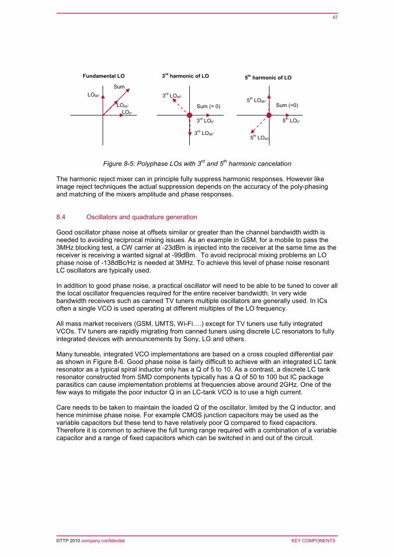
67
©TTP 2010 company confidential KEY COMPONENTS
Figure 8-5: Polyphase LOs with 3rd and 5th harmonic cancelation The harmonic reject mixer can in principle fully suppress harmonic responses. However like image reject techniques the actual suppression depends on the accuracy of the poly-phasing and matching of the mixers amplitude and phase responses. 8.4 Oscillators and quadrature generation Good oscillator phase noise at offsets similar or greater than the channel bandwidth width is needed to avoiding reciprocal mixing issues. As an example in GSM, for a mobile to pass the 3MHz blocking test, a CW carrier at -23dBm is injected into the receiver at the same time as the receiver is receiving a wanted signal at -99dBm. To avoid reciprocal mixing problems an LO phase noise of -138dBc/Hz is needed at 3MHz. To achieve this level of phase noise resonant LC oscillators are typically used. In addition to good phase noise, a practical oscillator will need to be able to be tuned to cover all the local oscillator frequencies required for the entire receiver bandwidth. In very wide bandwidth receivers such as canned TV tuners multiple oscillators are generally used. In ICs often a single VCO is used operating at different multiples of the LO frequency. All mass market receivers (GSM, UMTS, Wi-Fi….) except for TV tuners use fully integrated VCOs. TV tuners are rapidly migrating from canned tuners using discrete LC resonators to fully integrated devices with announcements by Sony, LG and others. Many tuneable, integrated VCO implementations are based on a cross coupled differential pair as shown in Figure 8-6. Good phase noise is fairly difficult to achieve with an integrated LC tank resonator as a typical spiral inductor only has a Q of 5 to 10. As a contrast, a discrete LC tank resonator constructed from SMD components typically has a Q of 50 to 100 but IC package parasitics can cause implementation problems at frequencies above around 2GHz. One of the few ways to mitigate the poor inductor Q in an LC-tank VCO is to use a high current. Care needs to be taken to maintain the loaded Q of the oscillator, limited by the Q inductor, and hence minimise phase noise. For example CMOS junction capacitors may be used as the variable capacitors but these tend to have relatively poor Q compared to fixed capacitors. Therefore it is common to achieve the full tuning range required with a combination of a variable capacitor and a range of fixed capacitors which can be switched in and out of the circuit.
Fundamental LO 3rd harmonic of LO 5th harmonic of LO Sum
Sum (=0) Sum (= 0)
LO90°
3rd LO90°
5th LO90° LO45°
LO0°
3rd LO45°
3rd LO0° 5th LO0°
5th LO45°

68
©TTP 2010 company confidential KEY COMPONENTS
Figure 8-6: Simplified differential VCO Using integrated BAW resonators for narrow band oscillators is a possible approach for high Q integrated oscillators. A high Q resonator resonance frequency can easily be modified resulting in an oscillator only being capable of being tuned over a very narrow band resulting in a receiver with a very narrow tuning range. However bandwidth widening techniques allowing up to a 10% band to be covered with a single VCO were reported at ISSCC200833
8.4.1 Quadrature generation
.
For any receiver using mixers operating in quadrature it is necessary to generate signals in quadrature to each other. Ideally these quadrature signals need to be phase and gain matched across the frequency band of interest. One of the simplest methods is to use an RC-CR filter as shown in Figure 8-7.
Figure 8-7: RC-CR filter With this type of circuit, assuming the two R’s and two C’s are matched there is exactly a 90° phase difference between I and Q at all frequencies. The magnitude response is different at all frequencies except at
33 Christophe Lilliard et al, “A 1V 220MHz-Tuning-Range 2.2GHz VCO Using a BAW Resonator” CEA-Leti-MINATEC, 2008
VIN I Q R
R C
C
VTUNE
IOUT+ iOUT-
VDD
RC1
=ω

69
©TTP 2010 company confidential KEY COMPONENTS
It is possible to couple together two differential VCO’s so that they oscillate in quadrature and obtain good phase noise. A phase noise of -140dBc/Hz at 3MHz operating at 1.57GHz has been reported with this technique using 0.35um CMOS34
A pair of integrators, in a feedback loop provide in principle perfect matched phase and amplitude as shown in
. Digital dividers can be used to generate quadrature signals. A divide by four approach makes the output insensitive to the duty cycle of the input signal. However this requires a very high frequency oscillator. For relatively low frequency receivers this may be a good approach as it allows the local oscillator inductors to be integrated. By generating the local oscillator at a different frequency to that used in the receiver the danger of the LO leaking from the antenna, or causing DC offset problems in zero IF and low IF receivers, is reduced.
Figure 8-8. This oscillator could be constructed from two op-amps. In practice due to additional poles, component variations etc the outputs tend not to be perfectly in quadrature although quadrature oscillators with phase error of less than 0.5° have been reported operating at up to 1GHz35
.
Figure 8-8: Quadrature oscillator block diagram Ring oscillators using 2, or 4 states can be used. These tend to have a low Q but can be used to tune over a wide frequency range. At high frequencies both integrators and ring oscillators are likely to produce too much phase noise. 8.4.2 Phase locked loops (PLL) A PLL allows a free running voltage controlled oscillator to be locked to an accurate crystal reference (typically ±20ppm) generally oscillating at a lower frequency. This allows the receiver’s LO to achieve an accuracy of ±20KHz, allowing the receive filters to be aligned fairly well. Often, especially in transceivers which also need to transmit, this accuracy is not sufficient. In a cellular system the crystal is replaced with a voltage controlled crystal oscillator, VCXO. The VCXO is tuned so that the transceiver is precisely aligned to the base station frequency. The crystal, or VCXO, will have much better phase noise close to its fundamental frequency than the VCO. Within the loop bandwidth of the PLL, the phase noise from the VCO will be suppressed by the loop filter. Outside the loop filter the VCO phase noise will dominate as shown in Figure 8-9. This allows the received signal to be down converted without adding significant phase jitter to the received constellation. Phase jitter can be a problem in OFDM systems with many carriers each modulated with a very low symbol rate high order QAM modulation. However PLLs tend to make little difference to reciprocal mixing where phase
34 Pan, Quan; 2008, “A 1.57GHz Low Power Low Phase Noise Quadrature LC-VCO”, WCECS, 22nd – 24th October 2008, San Francisco USA http://www.iaeng.org/publication/WCECS2008/WCECS2008_pp192-195.pdf [29th July 2009] 35 Lee, Thomas, 2004. “The Design of CMOS Radio Frequency Integrated Circuits, Second Edition”, Cambridge University Press, page 641
K/s -K/s

70
©TTP 2010 company confidential KEY COMPONENTS
noise at offsets similar or greater than the channel bandwidth (e.g. 200KHz for GSM) are significant.
Figure 8-9: Typical PLL phase noise 8.5 Discrete IF Filters 8.5.1 Quartz crystal filters The very high levels of Q exhibited by quartz resonators makes them ideal for use as the primary channel filter in high performance radio receivers. There frequency of operation is limited to typically 50MHz by the physical properties of the crystal. As the frequency of operation is fixed they are almost always used at an IF frequency 8.5.2 SAW IF filters SAW filters are described in detail in section 8.1.1. Key parameters for a SAW IF filter is its transition bandwidth (Bt). This is the area between the stop band and the passband found on both sides of the passband. Its steepness directly affects the receiver’s adjacent channel performance. A typical example is shown in Figure 8-10.
Phase noise from the VCO
Phase noise from the crystal
Loop bandwidth

71
©TTP 2010 company confidential KEY COMPONENTS
Figure 8-10: IF SAW filter frequency response (With permission, EPCOS X6792M)
IF filters, as they operate at lower frequencies tend to be quite large. For example a 36MHz SAW used for TV tuners typically measures around 17x 9 x 4mm. A limitation of their use is that their bandwidth is fixed. Therefore to cope with multiple channel bandwidths, for example to build a world TV tuner which needs bandwidths of 6, 7 and 8MHz, multiple filters are required. 8.6 Integrated amplifiers and active filters As well as an LNA, receiver ICs need a variety of amplifiers to amplify the signal to a level suitable for analogue to digital conversion, implement AGC circuits, interface to external filters and/or allow the use of active filters. These amplifiers and active filters must have:
• Adequate noise performance to not detrimentally affect the receivers noise figure
• Good linearity • Good repeatability (reduced sensitivity to component variations, or can be
calibrated) • Low power consumption • Adequate bandwidth
Noise figure is not as critical in post LNA stages and therefore allows other amplifier topologies to be used. Similarly, at low GHz radio frequencies unless stages need to be matched to an external device, as the size of the circuit element is small compared to the wavelength of interest reducing the importance of input and output impedance matching to a level where matching can often be neglected. Unless the receiver is operating with very little gain, the amplifier prior to channel filtering is generally the critical stage in the design defining the receiver’s large signal performance. After channel filtering, all the unwanted interfering signals should have been removed and the IIP3 of further amplifier stages can be relaxed. If a distributed gain and filtering approach is used as shown in Figure 6-12 the IIP3 of stages needs to be appropriately scaled as interferers are gradually suppressed and the signal amplified. If digital channel filtering is used all the analogue stages and ADC need adequate IIP3 and SFDR.

72
©TTP 2010 company confidential KEY COMPONENTS
Integrated filters tend to not use inductors as these do not lend themselves well to integration and take up a large area. Alternatively external inductors can be used with internal variable capacitors36
With image rejecting mixer based receiver architectures such as low IF and zero IF, matching of the amplifiers gain and any associated filter parameters becomes critical for good image rejection (discussed in section
. It is important that gain and bandwidth are well controlled across variations in process, supply voltage and temperature (PVT). The precise positioning of filter poles and zeros’s is critical to realising the desired filter response with the minimum number of poles, and therefore amplifier stages. This becomes especially important when the filter is implementing a channel filter and there needs to be adequate rejection of the adjacent channel to achieve the desired selectivity whilst not removing any of the wanted signal and therefore loosing sensitivity. In DAB, for instance, the wanted channel bandwidth is 1.54MHz wide. A 176 KHz guard band is inserted between adjacent channels. The standard EN50248:2001 requires greater than 30dB of adjacent channel rejection. To achieve this filtering, positioning of the filter cut off frequency to within a few Kilohertz or tens of Kilohertz is required. If a zero IF approach is used, the channel filter needs to cut off at 770KHz. Allowing say a 20 KHz spread in the cut off frequency in the design means a filter tolerance of better than 2.5% is required. This tolerance is far more stringent than what can be implemented in a silicon process and some form of calibration is typically used. If a low IF architecture is used the tolerance requirement will be greater as the cut off frequency is higher.
6.1.4). Calibration either at power on, or during receiver idle periods, feedback techniques such as AGC, and voltage and temperature monitoring techniques are all used to enhance the circuit performance helping overcoming PVT issues. This will be discussed in section 8.6.3 below. Most receiver architectures, assuming the LNA has sufficient power gain to overcome the mixers noise figure and conversion gain/loss, allocate the majority of the receiver gain required to be at IF or baseband frequencies. Historically, with limited gain available at RF frequencies this was a prerequisite of any design. However with improved transistor fT’s this is less of a limitation allowing more active circuits to be used at higher RF frequencies. This is likely to allow greater frequency selectivity prior to mixing, especially useful in wideband receivers where fixed frequency input filters are of limited use. It may be possible to bring the ADC much closer to the antenna allowing more digital filtering, assuming sufficient ADC sampling rates and dynamic range can be implemented. A variety of amplifier types and circuit topologies can be used. These will be discussed below. Almost always differential circuits are used making the structures less sensitive to common mode noise signals and even order intermodulation. 8.6.1 Amplifiers 8.6.1.i Operational amplifiers Operational amplifiers, as used in classic low frequency analogue signal processing have a high impedance input and low impedance output. They amplify the differential voltage at their input and produce a voltage output. Due to their limited bandwidth and high current consumption they are generally not used in RFICs.
36 Sony; 2008, “CMOS tuners for large screen TV sets” http://www.sony.net/Products/SC-HP/cx_news/vol56/pdf/featuring56.pdf [11th August 2009]
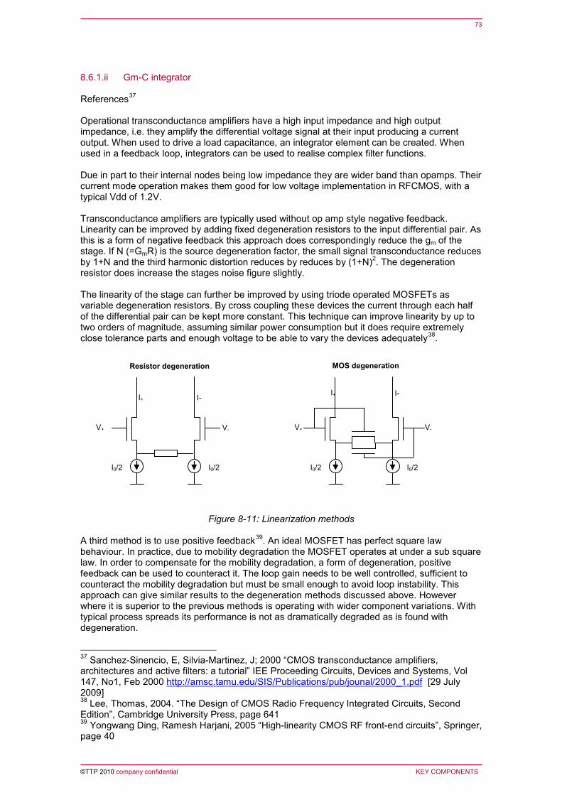
73
©TTP 2010 company confidential KEY COMPONENTS
8.6.1.ii Gm-C integrator References37
The linearity of the stage can further be improved by using triode operated MOSFETs as variable degeneration resistors. By cross coupling these devices the current through each half of the differential pair can be kept more constant. This technique can improve linearity by up to two orders of magnitude, assuming similar power consumption but it does require extremely close tolerance parts and enough voltage to be able to vary the devices adequately
Operational transconductance amplifiers have a high input impedance and high output impedance, i.e. they amplify the differential voltage signal at their input producing a current output. When used to drive a load capacitance, an integrator element can be created. When used in a feedback loop, integrators can be used to realise complex filter functions. Due in part to their internal nodes being low impedance they are wider band than opamps. Their current mode operation makes them good for low voltage implementation in RFCMOS, with a typical Vdd of 1.2V. Transconductance amplifiers are typically used without op amp style negative feedback. Linearity can be improved by adding fixed degeneration resistors to the input differential pair. As this is a form of negative feedback this approach does correspondingly reduce the gm of the stage. If N (=GmR) is the source degeneration factor, the small signal transconductance reduces by 1+N and the third harmonic distortion reduces by reduces by (1+N)2. The degeneration resistor does increase the stages noise figure slightly.
38
Figure 8-11: Linearization methods
.
A third method is to use positive feedback39
37 Sanchez-Sinencio, E, Silvia-Martinez, J; 2000 “CMOS transconductance amplifiers, architectures and active filters: a tutorial” IEE Proceeding Circuits, Devices and Systems, Vol 147, No1, Feb 2000
. An ideal MOSFET has perfect square law behaviour. In practice, due to mobility degradation the MOSFET operates at under a sub square law. In order to compensate for the mobility degradation, a form of degeneration, positive feedback can be used to counteract it. The loop gain needs to be well controlled, sufficient to counteract the mobility degradation but must be small enough to avoid loop instability. This approach can give similar results to the degeneration methods discussed above. However where it is superior to the previous methods is operating with wider component variations. With typical process spreads its performance is not as dramatically degraded as is found with degeneration.
http://amsc.tamu.edu/SIS/Publications/pub/jounal/2000_1.pdf [29 July 2009] 38 Lee, Thomas, 2004. “The Design of CMOS Radio Frequency Integrated Circuits, Second Edition”, Cambridge University Press, page 641 39 Yongwang Ding, Ramesh Harjani, 2005 “High-linearity CMOS RF front-end circuits”, Springer, page 40
V+ V-
I0/2 I0/2
V+
I0/2 I0/2
V-
I+ I- I+ I-
Resistor degeneration MOS degeneration
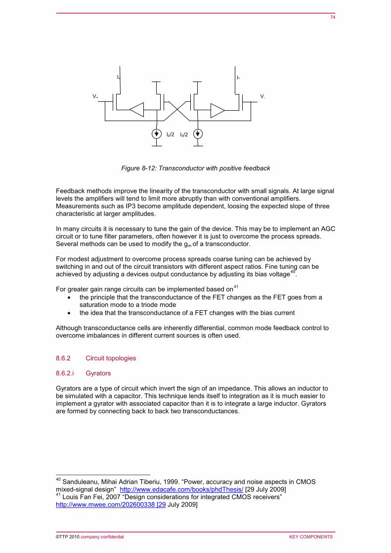
74
©TTP 2010 company confidential KEY COMPONENTS
Figure 8-12: Transconductor with positive feedback Feedback methods improve the linearity of the transconductor with small signals. At large signal levels the amplifiers will tend to limit more abruptly than with conventional amplifiers. Measurements such as IP3 become amplitude dependent, loosing the expected slope of three characteristic at larger amplitudes. In many circuits it is necessary to tune the gain of the device. This may be to implement an AGC circuit or to tune filter parameters, often however it is just to overcome the process spreads. Several methods can be used to modify the gm of a transconductor. For modest adjustment to overcome process spreads coarse tuning can be achieved by switching in and out of the circuit transistors with different aspect ratios. Fine tuning can be achieved by adjusting a devices output conductance by adjusting its bias voltage40
For greater gain range circuits can be implemented based on
.
41
• the principle that the transconductance of the FET changes as the FET goes from a saturation mode to a triode mode
• the idea that the transconductance of a FET changes with the bias current Although transconductance cells are inherently differential, common mode feedback control to overcome imbalances in different current sources is often used.
8.6.2 Circuit topologies 8.6.2.i Gyrators Gyrators are a type of circuit which invert the sign of an impedance. This allows an inductor to be simulated with a capacitor. This technique lends itself to integration as it is much easier to implement a gyrator with associated capacitor than it is to integrate a large inductor. Gyrators are formed by connecting back to back two transconductances.
40 Sanduleanu, Mihai Adrian Tiberiu, 1999. “Power, accuracy and noise aspects in CMOS mixed-signal design” http://www.edacafe.com/books/phdThesis/ [29 July 2009] 41 Louis Fan Fei, 2007 “Design considerations for integrated CMOS receivers” http://www.mwee.com/202600338 [29 July 2009]
V+
I0/2 I0/2
I+ I-
V-

75
©TTP 2010 company confidential KEY COMPONENTS
Figure 8-13: Gyrator It can be shown that:
2m
2
gC
=L
A pair of gyrators and a capacitor allow a floating series inductor to be created as might be used in an LC ladder filter circuit such as the one shown in Figure 8-13. The inductor can be tuned by setting the gm of the cell.
Figure 8-14: LC ladder filter Gm-C cells using this type of topology offer good high frequency performance. Simulations of a narrow band second order tuneable bandpass filter design operating over the entire UHF TV band based on the TSMC 0.13um CMOS process have been reported42
8.6.2.ii Biqaud filters
.
Biqaud filters can implement all types of filter responses and are typically implemented with a two-integrator-loop topology. They have less sensitivity to component variations compared to many other filter implementations. The higher the gm of the transconductance cell, the lower the capacitance is needed for a given pole frequency. This allows relatively low frequency filters to be implemented with small capacitors. The Q of the filter will be affected by the finite output impedance of the amplifier. 8.6.2.iii Switched capacitor Switched capacitor filters are constructed by substituting the resistors in an active RC filter with switches and capacitors. Assuming the switch is switched at a much faster rate than the analogue signal it is passing, the switch acts as a resistor allowing an RF type filter to be implemented. Switched capacitor filters have very precisely defined characteristics because the time constants associated with the frequency response depend only on the capacitor ratios and the clock frequency. Capacitor ratios can be well controlled within an IC. Clocks can be derived
42 Sun; Y, Lee; J, Lee, S; 2008 On-chip Active RF Tracking Filter with 60dB 3rd Order Harmonic Rejection for Digital TV Tuners” Int. SoC Design Conf http://rfcmos.icu.ac.kr/pdf/conferences/2008/9.pdf [29 July 2009]
V1 V2 C2 gmV2 gmV1
C2 C3 C1 Vin
L1 L2
76
©TTP 2010 company confidential KEY COMPONENTS
from a crystal so can be accurate to a few ppm. As switched capacitor filters sample the signal they need to be protected from alias frequencies in a similar way to an ADC. Since the opamps used in switched capacitor filters must have greater bandwidth than the signal they are processing, power consumption tends to be high. 8.6.3 Calibration Calibration can be used to help achieve optimum receiver performance. Calibration might be used to get good image rejection, for precisely setting stage gains to balance the sensitivity and selectivity performance of a receiver, or for setting more accurate corner frequencies of filters etc than can be obtained across the PVT variations of a silicon process. Calibration can be done using a wide range of techniques. These techniques allow looser tolerance on chip components to be used rather than more expensive, space consuming off chip parts. Calibration can be performed during production using specific test equipment and operating modes. Whilst highly automated it does take time, adding cost to the design. Production calibration can reduce effects due to process variations and possibly voltage variations. However temperature variations are difficult to account for quickly and any long term affects cannot be accounted for. Often it is desirable to implement receiver self calibration. For receiver self calibration known test signals often need to be generated and specific signals measured. These often entail the use of additional DACs and ADCs in the design. The baseband section is often used in a different way to its normal operating mode to measure specific signal levels. In a transceiver design the transmitter section can sometimes be used to generate the test signal to calibrate the receiver. Generally the receiver needs to be offline for full closed loop calibration. This can be done during initial power up, during gaps in reception, e.g. when time division multiplexing is used, or when the receiver is being retuned. If the receiver can’t be calibrated whilst operating, other techniques such as voltage and temperature monitoring can potentially be used. Assuming a circuit’s response to temperature or voltage is known, by monitoring these parameters during operation open loop adjustment of the circuit can be made as these parameters vary. Whilst calibration can improve the performance of a system there are usually some system limitations including:
• How accurately the error can be measured • The accuracy and resolution of the correcting parameter • Stability and drift with temperature, voltage time etc. • Second order effects, for instance the calibration may degrade some receiver
parameters whilst trying to improve others or the calibration may be optimum at one frequency, but not at others.
8.6.3.i Gain calibration Gain calibration can be done by injecting a known signal into a receiver and measuring the output. By using a DAC to generate the calibration reference signal, the signals amplitude can be as accurate as the reference voltage of the DAC, typically a few percent. Many designs use cascaded gain stages each likely to need individual calibration. Individual stage calibration can be achieved by shorting out one stage at a time so that the gain of each stage can be determined. Great care needs to be taken that each individual stage is calibrated under the same input and output load conditions as it will operate under. 8.6.3.ii Corner frequency calibration Integrated filters can typically be tuned offline to the correct corner frequency using ideally a precise frequency of known amplitude. The precise frequency is generally derived from the receiver’s crystal and is therefore accurate to a few ppm. The filters frequency can be changed by adjusting the gm of a cell or switching in and out additional capacitors.
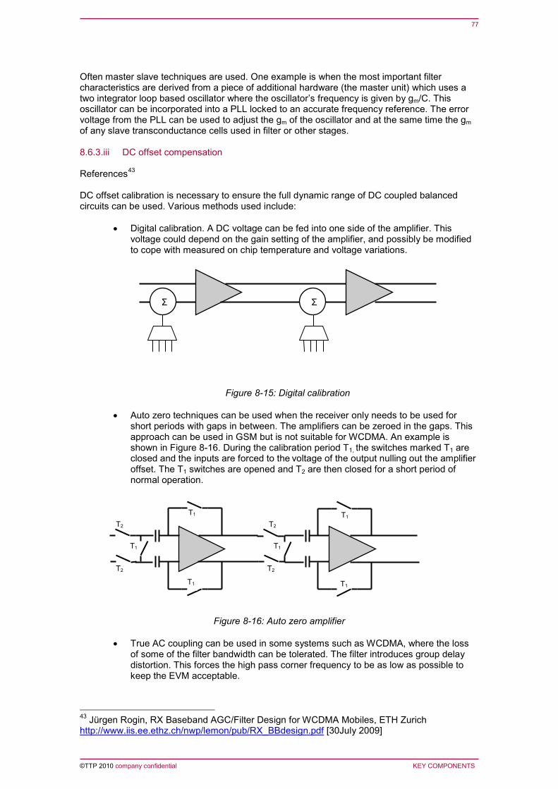
77
©TTP 2010 company confidential KEY COMPONENTS
Often master slave techniques are used. One example is when the most important filter characteristics are derived from a piece of additional hardware (the master unit) which uses a two integrator loop based oscillator where the oscillator’s frequency is given by gm/C. This oscillator can be incorporated into a PLL locked to an accurate frequency reference. The error voltage from the PLL can be used to adjust the gm of the oscillator and at the same time the gm of any slave transconductance cells used in filter or other stages. 8.6.3.iii DC offset compensation References43
• Digital calibration. A DC voltage can be fed into one side of the amplifier. This voltage could depend on the gain setting of the amplifier, and possibly be modified to cope with measured on chip temperature and voltage variations.
DC offset calibration is necessary to ensure the full dynamic range of DC coupled balanced circuits can be used. Various methods used include:
Figure 8-15: Digital calibration
• Auto zero techniques can be used when the receiver only needs to be used for
short periods with gaps in between. The amplifiers can be zeroed in the gaps. This approach can be used in GSM but is not suitable for WCDMA. An example is shown in Figure 8-16. During the calibration period T1, the switches marked T1 are closed and the inputs are forced to the voltage of the output nulling out the amplifier offset. The T1 switches are opened and T2 are then closed for a short period of normal operation.
Figure 8-16: Auto zero amplifier
• True AC coupling can be used in some systems such as WCDMA, where the loss of some of the filter bandwidth can be tolerated. The filter introduces group delay distortion. This forces the high pass corner frequency to be as low as possible to keep the EVM acceptable.
43 Jürgen Rogin, RX Baseband AGC/Filter Design for WCDMA Mobiles, ETH Zurich http://www.iis.ee.ethz.ch/nwp/lemon/pub/RX_BBdesign.pdf [30July 2009]
T1
T2 T2
T1
T2
T1
T1
T1
T1
T2
Σ Σ

78
©TTP 2010 company confidential KEY COMPONENTS
Figure 8-17: True AC coupling
• Highpass through a servo loop. The offset can be regulated by measuring the
output offset and subtracting it at the input using an integrator. The integrator time constant must be programmable to keep the high pass corner frequency constant for different gain settings.
Figure 8-18: Servo loop
8.7 Analogue to digital convertors A wide range of ADC architectures can be used in receivers. Sampling rate, resolution, and the speed of sample and hold circuits are all crucial to receiver performance. Sampling rate and resolution needs to be adequate to receive at a minimum the wanted received channel with adequate SINR to allow the signal to be decoded. The sample and hold circuit must be able to cope with the input signal frequency. To obtain full ADC performance suitable anti-alias filters must be implemented. To relax the anti-alias filter requirements, or if any adjacent channel selectivity is going to be implemented digitally, a higher sampling rate is needed than is needed just to sample the wanted channel. At the same time the ADC will need greater dynamic range to cope with out of band blockers. As has been discussed in section 4.4.3 sampling and resolution can be traded. This idea can be extended using sigma delta ADC’s discussed below. The quantisation noise level is a fundamental limit of data convertors and is defined by the number of bits of resolution the ADC has and the ADC’s full scale amplitude. Sampling jitter contributes additional noise degrading performance. For a sampling clock with a constant level of jitter the noise added is proportional to the clock frequency. Therefore clock jitter can be very significant at high sampling rates. An ADC’s voltage reference sets the full scale amplitude of an ADC. The reference voltage must be the same or less than the ADC supply voltage. Whilst quantisation noise and jitter are independent of the amplitude of the signal other thermal noise related mechanisms are dependent on the input signals amplitude. These mechanisms limit the practical dynamic range of a convertor with a limited supply voltage. One of these is KT/C noise and is associated with the thermal noise associated with the ADC’s sampling switch. As the sampling capacitor increases by k the noise reduces by the square root of k. Therefore for a high resolution a large sampling capacitor is required. For instance with a 1V Fs amplitude convertor a 0.8pF sampling
Σ
Σ
∫dt
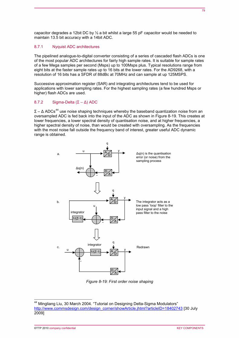
79
©TTP 2010 company confidential KEY COMPONENTS
capacitor degrades a 12bit DC by ½ a bit whilst a large 55 pF capacitor would be needed to maintain 13.5 bit accuracy with a 14bit ADC. 8.7.1 Nyquist ADC architectures The pipelined analogue-to-digital converter consisting of a series of cascaded flash ADCs is one of the most popular ADC architectures for fairly high sample rates. It is suitable for sample rates of a few Mega samples per second (Msps) up to 100Msps plus. Typical resolutions range from eight bits at the faster sample rates up to 16 bits at the lower rates. For the AD9268, with a resolution of 16 bits has a SFDR of 88dBc at 70MHz and can sample at up 125MSPS. Successive approximation register (SAR) and integrating architectures tend to be used for applications with lower sampling rates. For the highest sampling rates (a few hundred Msps or higher) flash ADCs are used. 8.7.2 Sigma-Delta (Σ – Δ) ADC Σ – Δ ADCs44
Figure 8-19 use noise shaping techniques whereby the baseband quantization noise from an
oversampled ADC is fed back into the input of the ADC as shown in . This creates at lower frequencies, a lower spectral density of quantisation noise, and at higher frequencies, a higher spectral density of noise, than would be created with oversampling. As the frequencies with the most noise fall outside the frequency band of interest, greater useful ADC dynamic range is obtained.
Figure 8-19: First order noise shaping
44 Mingliang Liu, 30 March 2004. “Tutorial on Designing Delta-Sigma Modulators” http://www.commsdesign.com/design_corner/showArticle.jhtml?articleID=18402743 [30 July 2009]
y u
-
A D
D A
q
Δq(n)
y
u
-
A D
D A
q
1/(Z-1)
y u
- A D
D A
q
1/(Z-1)
a.
integrator
integrator
b.
c.
Δq(n) is the quantisation error (or noise) from the sampling process
The integrator acts as a low pass ‘loop’ filter to the input signal and a high pass filter to the noise
Redrawn
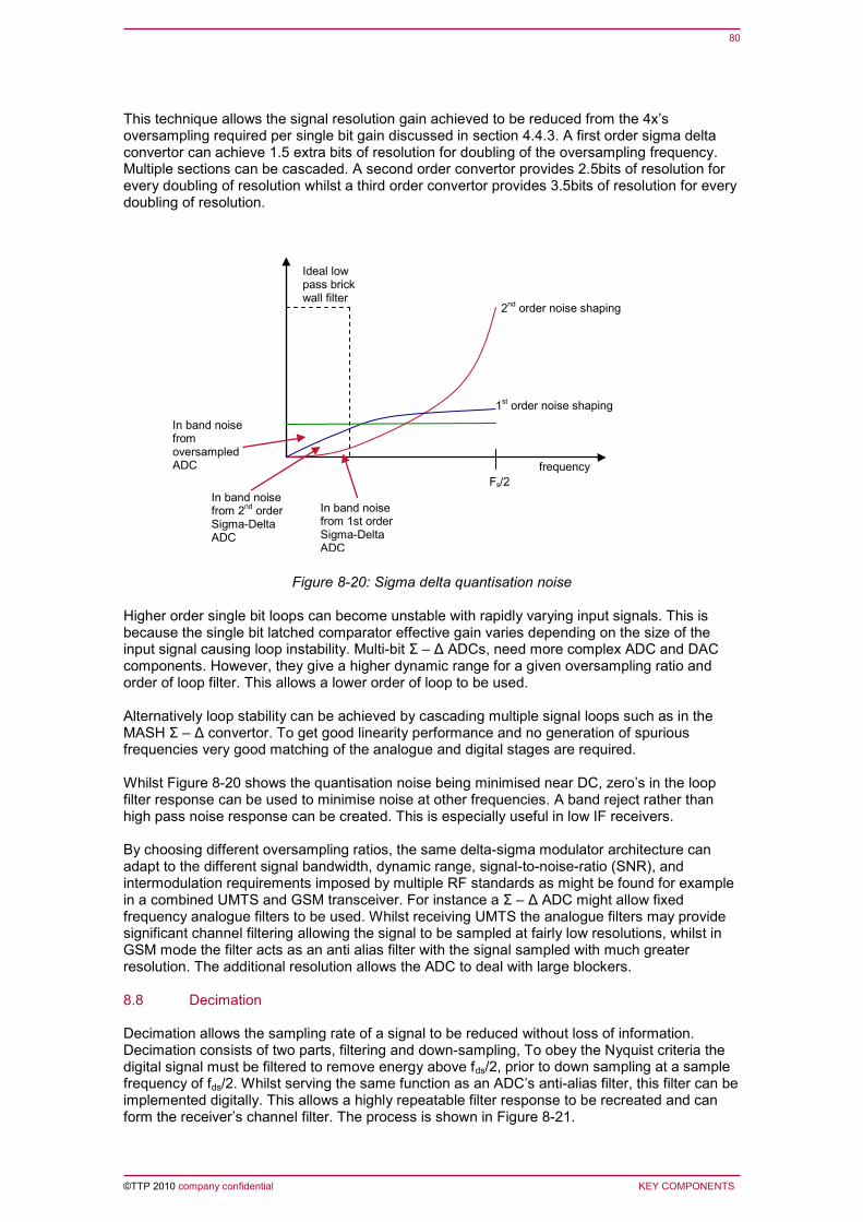
80
©TTP 2010 company confidential KEY COMPONENTS
This technique allows the signal resolution gain achieved to be reduced from the 4x’s oversampling required per single bit gain discussed in section 4.4.3. A first order sigma delta convertor can achieve 1.5 extra bits of resolution for doubling of the oversampling frequency. Multiple sections can be cascaded. A second order convertor provides 2.5bits of resolution for every doubling of resolution whilst a third order convertor provides 3.5bits of resolution for every doubling of resolution.
Figure 8-20: Sigma delta quantisation noise Higher order single bit loops can become unstable with rapidly varying input signals. This is because the single bit latched comparator effective gain varies depending on the size of the input signal causing loop instability. Multi-bit Σ – Δ ADCs, need more complex ADC and DAC components. However, they give a higher dynamic range for a given oversampling ratio and order of loop filter. This allows a lower order of loop to be used. Alternatively loop stability can be achieved by cascading multiple signal loops such as in the MASH Σ – Δ convertor. To get good linearity performance and no generation of spurious frequencies very good matching of the analogue and digital stages are required. Whilst Figure 8-20 shows the quantisation noise being minimised near DC, zero’s in the loop filter response can be used to minimise noise at other frequencies. A band reject rather than high pass noise response can be created. This is especially useful in low IF receivers. By choosing different oversampling ratios, the same delta-sigma modulator architecture can adapt to the different signal bandwidth, dynamic range, signal-to-noise-ratio (SNR), and intermodulation requirements imposed by multiple RF standards as might be found for example in a combined UMTS and GSM transceiver. For instance a Σ – Δ ADC might allow fixed frequency analogue filters to be used. Whilst receiving UMTS the analogue filters may provide significant channel filtering allowing the signal to be sampled at fairly low resolutions, whilst in GSM mode the filter acts as an anti alias filter with the signal sampled with much greater resolution. The additional resolution allows the ADC to deal with large blockers. 8.8 Decimation Decimation allows the sampling rate of a signal to be reduced without loss of information. Decimation consists of two parts, filtering and down-sampling, To obey the Nyquist criteria the digital signal must be filtered to remove energy above fds/2, prior to down sampling at a sample frequency of fds/2. Whilst serving the same function as an ADC’s anti-alias filter, this filter can be implemented digitally. This allows a highly repeatable filter response to be recreated and can form the receiver’s channel filter. The process is shown in Figure 8-21.
Ideal low pass brick wall filter
Fs/2
In band noise from oversampled ADC
In band noise from 2nd order Sigma-Delta ADC
In band noise from 1st order Sigma-Delta ADC
1st order noise shaping
2nd order noise shaping
frequency
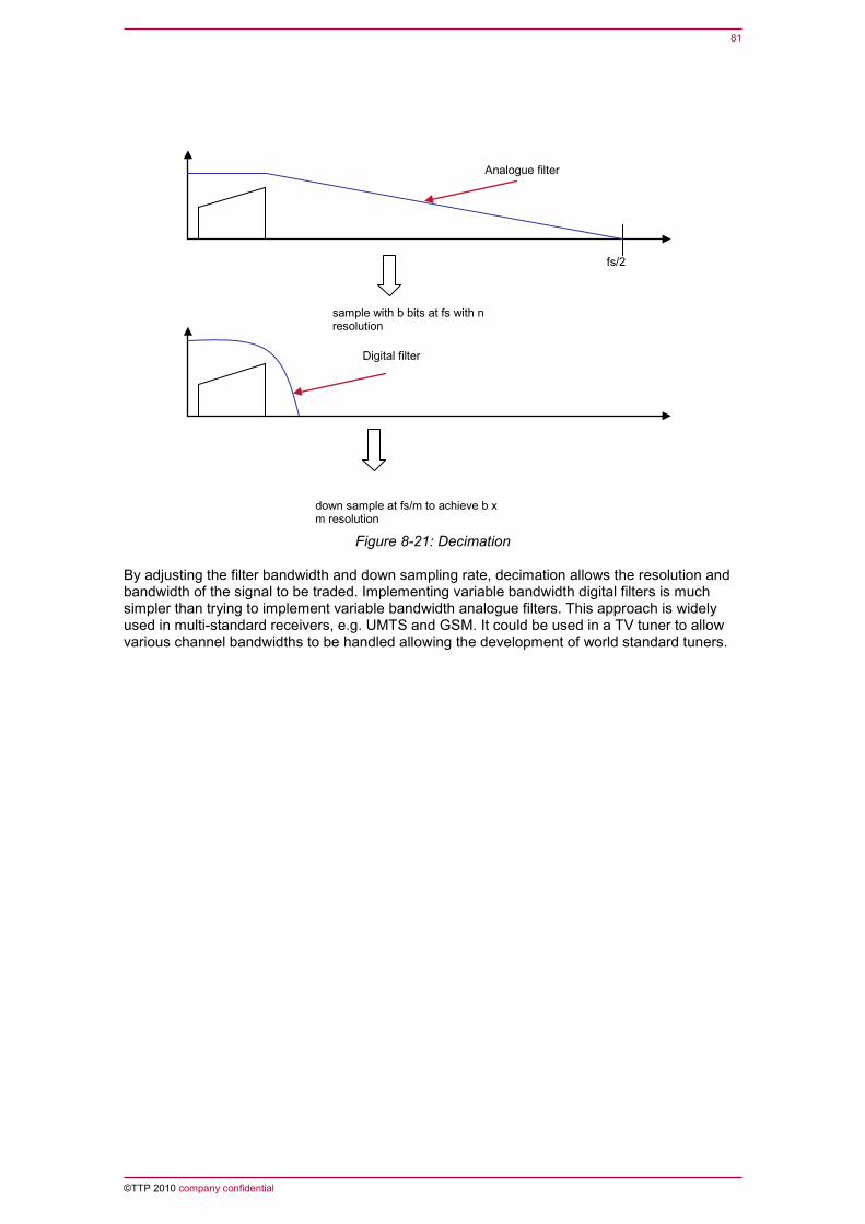
81
©TTP 2010 company confidential
Figure 8-21: Decimation
By adjusting the filter bandwidth and down sampling rate, decimation allows the resolution and bandwidth of the signal to be traded. Implementing variable bandwidth digital filters is much simpler than trying to implement variable bandwidth analogue filters. This approach is widely used in multi-standard receivers, e.g. UMTS and GSM. It could be used in a TV tuner to allow various channel bandwidths to be handled allowing the development of world standard tuners.
sample with b bits at fs with n resolution
down sample at fs/m to achieve b x m resolution
Analogue filter
Digital filter
fs/2

Lewis Davies Paul Winter

TTP is the premier independent technology and product development company. We work in partnership with our clients to bring new products to market, creating new business from advances in technology. Our partners include some of the world’s largest and most successful companies as well as some of the smallest and most ambitious.