OBJECTIVE PAPER-IIgfweb.s3.amazonaws.com/iespapers/2016/IES-Previous Year Objecti… · The unit...
24
ESE-2016 |EC| Objective Paper-II ICP–Intensive Classroom Program IES-Live Internet Based Classes DLP All India IES-Test Series Leaders in IES Preparation 65+ Centers across India © All rights reserved by Gateforum Educational Services Pvt. Ltd. No part of this booklet may be reproduced or utilized in any form without the written permission. 1 1. The closed-loop transfer function of a certain control system is given by 2 C 100 (s) . R s 10s 100 Then the settling time for a 2% tolerance band is given by (A) 0.8 s (B) 1.2 s (C) 1.5 s (D) 2.1 s Key: (A) Sol: 2 C 100 (s) R s 10s 100 Settling time for 2% tolerance 4 s 1/5 t 4 4/5 0.8s 2. The unit step input response of a certain control system is given by 60t 10t c(t) 1 0.2e 1.2e . The undamped natural frequency n and damping ratio are, respectively (A) 24.5 and 1.27 (B) 33.5 and 1.27 (C) 24.5 and 1.43 (D) 33.5 and 1.43 Key: (C) Sol: The step response c(t) 1 0.2e 60t 1.2e 10t then n and are. c(t) = 1+0.2e –60t – 1.2e -10t Impulse response 60t 10t 60 10t d h(t) c(t) dt dc(t) 0 (0.2)( 60)e 1.2( 10)e dt h(t) 12e 12e Then transfer function n n 24.49rad / sec 2 70 70 1.429 2(24.49) 2 1 1 50 12 12 s 10 s 60 s 70s 600 2 2 n 600 s 70s 600 600 3. In Force-Voltage Analogy (A) Force is analogous to current (B) Mass is analogous to capacitance (C) Velocity is analogous to current (D) Displacement is analogous to magnetic flux linkage Key: (C) Sol: In force- voltage analogy Velocity analogous to current 4. For a unity feedback control system having an open-loop transfer function 25 G(s) , s(s 6) what is the time t p at which the peak of the step input response occurs? (A) 0.52s (B) 2.75s (C) 0.79s (D) 1.57s Key: (C) Sol: 25 G(s)H(s) s(s 6) 2 n d p d C.E 1 GH s 6s 25 0 5, 0.6, 4 t 0.79sec 5. The transfer function 10(s 1) G(s) (s 10) represents (A) Unstable system (B) Minimum phase system (C) Non-minimum phase system (D) PID controller system Key: (C) OBJECTIVE PAPER-II
Transcript of OBJECTIVE PAPER-IIgfweb.s3.amazonaws.com/iespapers/2016/IES-Previous Year Objecti… · The unit...

ESE-2016 |EC| Objective Paper-II
ICP–Intensive Classroom Program IES-Live Internet Based Classes DLP All India IES-Test Series Leaders in IES Preparation 65+ Centers across India
© All rights reserved by Gateforum Educational Services Pvt. Ltd. No part of this booklet may be reproduced or utilized in any form without the written permission.
1
1. The closed-loop transfer function of a certain
control system is given by
2
C 100(s) .
R s 10s 100
Then the settling
time for a 2% tolerance band is given by
(A) 0.8 s (B) 1.2 s (C) 1.5 s (D) 2.1 s
Key: (A)
Sol: 2
C 100(s)
R s 10s 100
Settling time for 2% tolerance 4
s
1/ 5
t 4 4 / 5 0.8s
2. The unit step input response of a certain
control system is given by 60t 10tc(t) 1 0.2e 1.2e . The undamped
natural frequency n and damping ratio
are, respectively
(A) 24.5 and 1.27 (B) 33.5 and 1.27
(C) 24.5 and 1.43 (D) 33.5 and 1.43
Key: (C)
Sol: The step response
c(t) 1 0.2e 60t
1.2e10t
then n and are.
c(t) = 1+0.2e–60t
– 1.2e-10t
Impulse response
60t 10t
60 10t
dh(t) c(t)
dt
dc(t)0 (0.2)( 60)e 1.2( 10)e
dt
h(t) 12e 12e
Then transfer function
n
n
24.49rad / sec
2 70
701.429
2(24.49)
2
1 1 5012 12
s 10 s 60 s 70s 600
2
2
n
600
s 70s 600
600
3. In Force-Voltage Analogy
(A) Force is analogous to current
(B) Mass is analogous to capacitance
(C) Velocity is analogous to current
(D) Displacement is analogous to magnetic
flux linkage
Key: (C)
Sol: In force- voltage analogy Velocity analogous
to current
4. For a unity feedback control system having
an open-loop transfer function
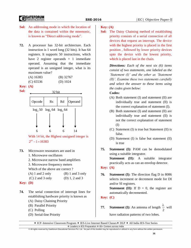
25G(s) ,
s(s 6)
what is the time tp at which
the peak of the step input response occurs?
(A) 0.52s (B) 2.75s
(C) 0.79s (D) 1.57s
Key: (C)
Sol: 25
G(s)H(s)s(s 6)
2
n d
p
d
C.E 1 GH s 6s 25 0
5, 0.6, 4
t 0.79sec
5. The transfer function 10(s 1)
G(s)(s 10)
represents
(A) Unstable system
(B) Minimum phase system
(C) Non-minimum phase system
(D) PID controller system
Key: (C)
OBJECTIVE PAPER-II

ESE-2016 |EC| Objective Paper-II
ICP–Intensive Classroom Program IES-Live Internet Based Classes DLP All India IES-Test Series Leaders in IES Preparation 65+ Centers across India
© All rights reserved by Gateforum Educational Services Pvt. Ltd. No part of this booklet may be reproduced or utilized in any form without the written permission.
2
Sol: 10(s 1)
G(s)(s 10)
Represents
Single right side zero means non-minimum
phase
6. What is the maximum input frequency limit
of a 3-bit Ripple counter configured around
flip-flops, with inherent propagation delay
time t pd = 50 ns?
(A) 6670 MHz (B) 667 MHz
(C) 66.7 MHz (D) 6.67 MHz
Key: (D)
Sol: clk 9
pd
1 1f 6.67MHz
N.t 3 50 10
7. The characteristic equation of a certain
feedback control system is given by
4 3 2s 4s 13s 36s k 0. The range of
values of k for which the feedback system is
stable, is given by
(A) 0 < k < 4 (B) 4 < k < 36
(C) 0 < k < 36 (D) 13 < k < 36
Key: (C)
Sol: s4+4s
3+13s
2+36s+k=0. Then the system is
stable for
The system is stable, when the first column
elements are positive.
36 k
k 0
0 k 36
8. The closed-loop transfer function of a unity
feedback control system is,
2
n
2 2
n n
C(s).
R(s) s s
The velocity error constant of the system is
(A) n
2
(B) n
(C) n2
(D) n3
2
Key: (A)
Sol:
2
n
2 2
n n
C(s)
R(s) s 2 s
2
n
n
G(s)s(s 2 )
The velocity error constant
vs 0
2 2
n n
s 0n n
nv
k limsG(s)
lim(s 2 ) 2
k2
9. The system described by the following state
equations
0 1 0
X X u, Y [1,1]X2 3 1
is
1. Completely controllable
2. Completely observable
Which of the above statements is/are
correct?
(A) 1 only (B) 2 only
(C) Both 1 and 2 (D) Neither 1 nor 2
Key: (C)
Sol: 0 1 0
X X U2 3 1
c
c
c
Y [1,1]x
Q B AB
0 1 0 1 0 1AB Q
2 2 1 31 3
Det Q 1 0 Controllable
0 1
CA [1 1]2 3
10 1
4
3
2
1
0
1 13 ks4 36 0
s4 k 0
s36 k
s 0 04
s k 0 0

ESE-2016 |EC| Objective Paper-II
ICP–Intensive Classroom Program IES-Live Internet Based Classes DLP All India IES-Test Series Leaders in IES Preparation 65+ Centers across India
© All rights reserved by Gateforum Educational Services Pvt. Ltd. No part of this booklet may be reproduced or utilized in any form without the written permission.
3
0
0
[2 2]
1 1Q
2 2
det Q 2 2 4 0
Observable
10. Consider the system with 2
k(s 2)G(s)
s 2s 3
and H(s) = 1. The breakaway point(s) of the
root loci is/are at
(A) –0.265 only
(B) –3.735 only
(C) –3.735 and –0.265
(D) There is no breakaway point
Key: (D)
Sol: 2
k(s 2)G(s)
s 2s 3
The Breakaway point of the system is
2
k(s 2)1
s 2s 3
s 2, 1 j 2
2
2
2
2 2
2
2
2
(s 2s 3)k
s 2
(s 2)(2s 2) s 2s 3dk0
ds (s 2)
2s 2s 4s 4 s 2s 3dk
ds (s 2)
s 4s 1k ' 0
(s 2)
Break points
s2 +4s+1=0
s = –0.26
s= –3.73
s = –0.26 is not on root locus therefore it is
not valid
s = –3.73 is break in point where the Root
locus branches are coming from complex
plane to real axis. Therefore there are no
break away points in the system.
11. How would a binary number 0010 be
represented by a 4-bit binary word, if the
range of voltage is 0 to 10 V?
(A) 0.666 V (B) 1.333 V
(C) 0.333 V (D) 2.000 V
Key: (B)
Sol: Full scale voltage =10 V
n 4
Full Scale output 10 10Resolution
2 1 2 1 15
Voltage for binary number (0010)2 =
22 1.333V
3
12. For a unity feedback system with open-loop
transfer function25
,s(s 6)
the resonant peak
output Mm and the corresponding resonant
frequency m, are respectively
(A) 2.6 and 2.64 rad/sec
(B) 1.04 and 2.64 rad/sec
(C) 2.6 and 4.8 rad/sec
(D) 1.04 and 4.8 rad/sec
Key: (B)
Sol: 25
G(s)s(s 6)
2
n
n
C(s) 25
R(s) s 6s 25
5
62 6 0.6
10
m2
1M
2 1
1
2(0.6) 1 0.6
11.04
2(0.6) 0.64
5 2
j 2
j 2
1

ESE-2016 |EC| Objective Paper-II
ICP–Intensive Classroom Program IES-Live Internet Based Classes DLP All India IES-Test Series Leaders in IES Preparation 65+ Centers across India
© All rights reserved by Gateforum Educational Services Pvt. Ltd. No part of this booklet may be reproduced or utilized in any form without the written permission.
4
2
m n 1 2
25 1 2(0.6) 2.645 rad / sec
13. The transfer function of a control system is
said to be ‘All Pass System’, if it has
(A) Unit magnitude at all frequencies with
anti-symmetric pole-zero pattern
(B) Unit magnitude at all frequencies with
symmetric pole-zero pattern
(C) Magnitude varying with frequency and
with anti-symmetric pole-zero pattern
(D) Unit magnitude at some frequencies
with symmetric pole-zero pattern
Key: (A)
Sol:
Pole zero pattern is anti-symmetric about
imaginary axis.
14. Consider the following:
1. Bode plot
2. Nyquist plot
3. Nichols chart
Which of the above frequency response plots
are commonly employed in the analysis of
control systems?
(A) 1 and 2 only (B) 1 and 3 only
(C) 2 and 3 only (D) 1, 2 and 3
Key: (D)
15. An A-to-D converter in which one sub-
circuit is a D-to-A converter is
(A) Parallel A/D converter
(B) Dual slope A/D converter
(C) Successive approximation A/D
converter
(D) Extended parallel type A/D converter
Key: (C)
16. Consider the transfer function:
2
2 2
5 s 10s 100G(s)
s (s 15s 1)
The corner frequencies in Bode’s plot for
this transfer function are as
(A) 10 rad/sec and 10 rad/sec
(B) 100 rad/sec and 10 rad/sec
(C) 10 rad/sec and 1 rad/sec
(D) 100 rad/sec and 1 rad/sec
Key: (C)
Sol: 2
2 2
5 s 10s 100G(s)
s (s 15s 1)
The corner frequencies of Bode plot
n = 10,
10 rad/sec , 1rad/sec
17. Consider the transfer function (0.1 + 0.01s)
for a PD controller. What is the frequency at
which the magnitude is 20 dB (by using
asymptotic Bode’s plot) ?
(A) 2000 r/s (B) 1000 r/s
(C) 200 r/s (D) 100 r/s
Key: (B)
Sol: G(s) = (0.1+0.01s)
The frequency at which the magnitude is
20dB
G(s) = 0.1 [1+0.1s]
Asymptotic magnitude
Masy = 20log [0.1] + 20log [0.1 ] = 20
2
20log[0.1 ] 40
0.1 10
1000rad / sec
18. The main objectives of drawing the root
locus plot are
1. To obtain a clear picture of the open-loop
poles and zeros of the system
2. To obtain a clear picture of the transient
response of the system for varying gain, K

ESE-2016 |EC| Objective Paper-II
ICP–Intensive Classroom Program IES-Live Internet Based Classes DLP All India IES-Test Series Leaders in IES Preparation 65+ Centers across India
© All rights reserved by Gateforum Educational Services Pvt. Ltd. No part of this booklet may be reproduced or utilized in any form without the written permission.
5
3. To find the range of K to make the system
stable
Which of the above statements are correct?
(A) 1, 2 and 3 (B) 1 and 2 only
(C) 1 and 3 only (D) 2 and 3 only
Key: (D)
Sol: Root locus main objectives
1. The open-loop poles zeros location is
known with simple s-plane. The Root
locus will give clear picture of closed
loop-poles movement.
2. To obtain clear picture of transient
response of the system with gain K.
3. To find the range of K to make the
system stable.
19. A unity feedback system has open-lop poles
at s = –2 j2, s = –1 and s = 0 and a zero at s
= –3. What are the angles made by the root-
loci asymptotes with the real axis?
(A) 60° , 180o and –60
o
(B) 30o , 90
o and 60
o
(C) 60o , 120
o and –30
o
(D) 30o , 60
o and 180
o
Key: (A)
Sol: s = –2 j2
s = – 1
s = 0
are poles of the system s = –3 is zero of the
system.
The asymptotes are
p =4 number of poles
z = 1 number of zeros
p–z = 3
o(2q 1)180
, q 0,1,2.... p z 1p z
Asymptotes are = 60, 180, 300°
20. The open-loop transfer function of a unity
feedback system is G(s)K
.s(s 5)
The gain
K that results in a phase margin of 45o is
(A) 35 (B) 30 (C) 25 (D) 20
Key: (A)
Sol: The K value such that phase margin is = 45
Phase margin pm
o o
pm sys gc
o
pm gc
180 ( ) 45
( ) 135
o 1
sys
gco 1
sys gc
gco 1 o
gc
2
gc2
gc gc
( ) 90 tan5
( ) 90 tan5
90 tan 1355
5
Magnitude
KM
25
KM( ) 1
5
K 5 25 25 35.35
21. From the Nichols chart, one can determine
the following quantities pertaining to a
closed-loop system:
(A) Magnitude, bandwidth and phase
(B) Bandwidth and phase only
(C) Magnitude and phase only
(D) Bandwidth only
Key: (A)
Sol: Nichols chart is used for finding the
magnitude, phase and BW
22. In position control systems, the Tacho-
generator feedback is used to
(A) Increase the effective damping in the
system
(B) Decrease the effective damping in the
system
(C) Decrease the Steady state error
(D) Increase the steady state error

ESE-2016 |EC| Objective Paper-II
ICP–Intensive Classroom Program IES-Live Internet Based Classes DLP All India IES-Test Series Leaders in IES Preparation 65+ Centers across India
© All rights reserved by Gateforum Educational Services Pvt. Ltd. No part of this booklet may be reproduced or utilized in any form without the written permission.
6
Key: (A)
Sol: Tacho-generator feedback is example for D
controller. Derivative controller reduces
ripples in the response i.e., maximum peak
over shoot reduces.
effective damping increases
23. Consider the following statements:
1. The pin diode consists of two narrow,
but highly doped, semiconductor
regions separated by a thicker, lightly
doped material called the intrinsic
region.
2. Silicon is used most often for its power
handling capability and because it
provides a highly resistive intrinsic
region.
3. The pin diode acts as an ordinary diode
at frequencies above 100 MHz.
Which of the above statements are correct?
(A) 1 and 2 only (B) 1 and 3 only
(C) 2 and 3 only (D) 1, 2 and 3
Key: (A)
Sol: The pin diode acts as an ordinary diode at
frequencies up to about 100MHz, but above
this frequency the operational characteristics
changes and begins acting as a variable
resistance.
24. Consider the following statements:
1. Additional cavities serve to velocity
modulate the electron beam and produce
an increase in the energy available at the
output.
2. The addition of intermediate cavities
between the input and output cavities of
the basic klystron greatly improves the
amplification, power output, and
efficiency of the klystron.
Which of the above statements is/are
correct?
(A) 1 only (B) 2 only
(C) Both 1 and 2 (D) neither 1 nor 2
Key: (C)
25. In a waveguide with perfectly conducting
flat wall, the angle of reflection is equal to
the angle of
(A) Diffraction (B) Incidence
(C) Refraction (D) Penetration
Key: (B)
Sol: In a waveguide with perfectly conducting
flat wall, the angle of reflection is equal to
the angle of incidence.
26. In microwave system, waveguides have the
advantages of
(A) High power-handling capability and low
loss
(B) Thin dielectric substrate
(C) Low power-handling and adequate
stability
(D) Positive phase shift
Key: (A)
27. A straight dipole radiator fed in the centre
will produce maximum radiation at
1. The plane parallel to its axis
2. The plane normal to its axis
3. Extreme ends
Which of the above statements is/are
correct?
(A) 1 only (B) 2 only
(C) 1 and 3 only (D) 2 and 3 only
Key: (B)
28. In communication systems, modulation is
the process of
(A) Improving frequency stability of
transmitter
(B) Combining message signal and radio
frequency waves

ESE-2016 |EC| Objective Paper-II
ICP–Intensive Classroom Program IES-Live Internet Based Classes DLP All India IES-Test Series Leaders in IES Preparation 65+ Centers across India
© All rights reserved by Gateforum Educational Services Pvt. Ltd. No part of this booklet may be reproduced or utilized in any form without the written permission.
7
(C) Generating constant frequency radio
waves
(D) Reducing distortion in RF waves
Key: (B)
Sol: Modulation is a process of changing the
characteristic of carrier signal (radio
frequency) with respect to message signal.
29. Which one of the following statements is
correct?
(A) Sampling and quantization operate in
amplitude domain
(B) Sampling and quantization operate in
time domain.
(C) Sampling operates in time domain and
quantization operates in amplitude
domain.
(D) Sampling operates in amplitude domain
and quantization operates in time
domain.
Key: (C)
Sol: Sampling discretize the time axis.
Quantization discretize the amplitude axis.
30. What is the voltage attenuation provided by
a 25 cm length of waveguide having a = 1
cm and b = 0.5 cm in which a 1 GHz signal
is propagated in the dominant mode?
(A) 721 dB (B) 681 dB
(C) 521 dB (D) 481 dB
Key: (B)
Sol: Given a = 1cm; b = 0.5cm
2
2
c
C
25cm 25 0 m
2a 2cm 2 10 m
Attenuation 54.5
2554.5 dB
2
681.25dB
l
31. When a plane wave travelling in free-space
is incident normally on a medium having
r = 9.0 and r = 1.0, the fraction of power
transmitted into the medium is
(A) 4
3 (B)
3
4 (C)
1
2 (D)
1
3
Key: (B)
Sol: 1 22 1
2 1 1 2
1 3 1
1 3 2
Fraction of transmitted power
2 1 31 1
4 4
32. A microwave antenna with the absorbing
cross-section area (A) and the power flux
density (S) in the incident wave is employed
as an absorber. The absorbed power (P) of
the antenna is
(A) A
S (B)
S
A (C) SA (D)
S 1
A 1
Key: (C)
33. LASER beam of light essentially finds its
application in transmission of a signal in the
optical fiber communication systems due to
(A) Incredible speed of signal
communication
(B) Low loss transmission of the signal
(C) Inexpensive installation cost
(D) Bulk availability of LASER sources
Key: (A & B)
34. The controller which is highly sensitive to
noise is
(A) PI (B) PD
(C) Both PI and PD (D) Neither PI nor PD
Key: (B)
Sol: PD controller is very sensitive to noise
35. The 2’s complement representation of –17 is
(A) 100001 (B) 101111
(C) 110011 (D) 101110

ESE-2016 |EC| Objective Paper-II
ICP–Intensive Classroom Program IES-Live Internet Based Classes DLP All India IES-Test Series Leaders in IES Preparation 65+ Centers across India
© All rights reserved by Gateforum Educational Services Pvt. Ltd. No part of this booklet may be reproduced or utilized in any form without the written permission.
8
Key: (B)
Sol: –17 = 2’s comp of (+17) = ( st1 complement
+1)
= 2’s comp of (010001)
= 101111
36. The subtraction of two hexadecimal numbers
8416 – 2A16 results in
(A) 2B16 (B) 3A16 (C) 4B16 (D) 5A16
Key: (D)
Sol: 8416 – 2A16 = 5A16
16 10
16 10
16 10
(84) (132)
(2A) (42)
(5A) (90)
37. The Vestigial Side Band (VSB) modulation
is preferred in TV systems because
1. It reduces the bandwidth requirement to
half
2. It avoids phase distortion at low
frequencies
Which of the above statements is/are
correct?
(A) 1 only (B) 2 only
(C) Both 1 and 2 (D) Neither 1 nor 2
Key: (B)
Sol: Bandwidth in VSB is 1.25B, where B is
message signal bandwidth.
Phase distortion are reduced at low
frequency.
38. If, A = 60 and B = 3, then using C-
programming A >> B results in
(A) 11100000 (B) 00000111
(C) 00111111 (D) 01111000
Key: (B)
Sol: We have to do the right shifting of binary
equivalent of 60by 3 bit positions.
00111100>>3 00000111
39. What is the base of the numbers for the
following operation to be correct?
bb
b
(54)(13)
(4)
(A) 2 (B) 4 (C) 8 (D) 16
Key: (C)
Sol: bb
b
5413
4
(5b 4) (b 3)4
5b 4 4b 12
b 8
40. It is awkward to employ signed-magnitude
system in computer arithmetic, because
1. Sign and magnitude have to be handled
separately
2. It has two representations for ‘0’
Which of the above statements is/are
correct?
(A) 1 only (B) 2 only
(C) Both 1 and 2 (D) Neither 1 nor 2
Key: (B)
Sol: Statement 2 is correct.
The signed –magnitude system is used in
ordinary arithmetic but is awkward when
employed in computer arithmetic. Therefore,
the signed complement is normally used.
The 1’s complement imposes difficulties
because it has representations of 0 (+0 to -0)
41. A single-stage amplifier has a voltage gain
of 100. The load connected to the collector is
500 and its input impedance is 1 k. Two
such stages are connected in cascade through
an R-C coupling. The overall gain is
(A) 10000 (B) 6666.66
(C) 5000 (D) 1666.66
Key: (B)
Sol:
V1inR mg V1 outR inR V2
mg V2 outR
STAGE I STAGE II
OUTIN

ESE-2016 |EC| Objective Paper-II
ICP–Intensive Classroom Program IES-Live Internet Based Classes DLP All India IES-Test Series Leaders in IES Preparation 65+ Centers across India
© All rights reserved by Gateforum Educational Services Pvt. Ltd. No part of this booklet may be reproduced or utilized in any form without the written permission.
9
IN OUT
m OUT
R 1k , R 500
g R 100(Given)
m
100g 0.2s
500
Overall gain m OUT IN m OUTg R R .g R
1000 0.50.2 0.2 500
1.5
6666.66
42. Assuming VCE(Sat) = 0.3V for a Silicon
transistor at ambient temperature of 25C
and hFE = 50, the minimum base current IB
required to drive the transistor into
saturation for the circuit shown is
(A) 64 A (B) 78 A
(C) 94 A (D) 140 A
Key: (C)
Sol: Step: (1)
KVL for output section of the circuit
sat
sat
CE
c
5V V 5V 0.3VI 4.7mA
1k 1k
Step: (2)
Minimum Base current required to drive the
BJT into saturation, IBmin
sat satC C
Bmin
FE
I I 4.7mAI 94 A
h 50
43. Which of the following regions of operation
are mainly responsible for heating of the
transistor under switching operation?
1. Saturation region
2. Cut-off region
3. Transition from saturation to cut-off
4. Transition from cut-off to saturation
Select the correct answer using the codes
given below
(A) 1, 2, and 4 only (B) 1, 3, and 4 only
(C) 2 and 3 only (D) 1 and 3 only
Key: (B)
Sol: The heating of a transistor under switching
operation occurs during
Transition from saturation to cut-off
Transition from cut-off to saturation
Saturation region
44. In a sinusoidal oscillator, sustained
oscillations will be produced only if the loop
gain (at the oscillation frequency) is
(A) Less than unity but not zero
(B) zero
(C) Unity
(D) Greater than unity
Key: (C)
Sol: The condition for sustained oscillation in a
sinusoidal oscillator at a particular frequency
is Av = Loop gain = 1 (Bark hausen
criteria)
45. The Class-B push-pull amplifier is an
efficient two-transistor circuit, in which the
two transistors operate in the following way:
5V
1k
Q
BI
5V
BI
Q
CsatI 1k
CE satV

ESE-2016 |EC| Objective Paper-II
ICP–Intensive Classroom Program IES-Live Internet Based Classes DLP All India IES-Test Series Leaders in IES Preparation 65+ Centers across India
© All rights reserved by Gateforum Educational Services Pvt. Ltd. No part of this booklet may be reproduced or utilized in any form without the written permission.
10
(A) Both transistors operate in the active
region throughout the negative ac cycle
(B) Both transistors operate in the active
region for more than half-cycle but less
than a whole cycle
(C) One transistor conducts during the
positive half-cycle and the other during
the negative half-cycle
(D) Full supply voltage appears across each
of the transistors
Key: (C)
Sol: In a class-B push-pull amplifier, the
conduction angle of each transistor is 180o
(i.e.) Each transistor is biased to conduct for
ONE-HALF CYCLE OF INPUT SIGNAL
only. In other words,
During +Ve half cycle of input signal,
One transistor (Let Q1) is pulled into ON
state and the other transistor (Let Q2) is
pushed into OFF state.
During –Ve half-cycle of input, Q2 is
pulled into ON state and Q1 is pushed into
OFF state.
46. Consider the following statements regarding
Wien Bridge oscillator:
1. It has a larger bandwidth than the phase
shift oscillator.
2. It has a smaller bandwidth than the
phase shift oscillator.
3. It has 2 capacitors while the phase shift
oscillator has 3 capacitors.
4. It has 3 capacitors while the phase shift
oscillator has 2 capacitors.
Which of the above statements are correct?
(A) 1 and 3 only (B) 2 and 4 only
(C) 1 and 4 only (D) 2 and 3 only
Key: (A)
Sol: RC Phase shift Oscillator
Suitable for oscillations in Audio
frequency (AF) range, preferably upto 1
kHz.
Three identical RC sections are to be used
in the phase shift network to construct a
practical RC Phase shift oscillator.
Wien Bridge Oscillator
Suitable for Oscillations in AF range up
to 100kHz.
Two RC sections (One series RC & one
parallel RC) are used in the feedback
network
47. For normal operation of a transistor
(A) Forward bias the emitter diode and
reverse bias the collector diode
(B) Forward bias the emitter diode as well
as the collector diode
(C) Reverse bias the emitter diode as well as
the collector diode
(D) Reverse bias the emitter diode and
forward bias the collector diode
Key: (A)
Sol: Normal operation of a transistor is ACTIVE
REGION of operation
Emitter
Diode/
Emitter
junction,
JE
Collector
Diode/
Collector
junction
Region of
operation
R.B R.B Cut-off Region
F.B F.B Saturation
Region
F.B R.B Normal active
region
R.B F.B
Inverse (or)
Reverse
Active Region
48. Consider the following statements regarding
linear power supply:
1. It requires low frequency transformer.
2. It requires high frequency transformer.

ESE-2016 |EC| Objective Paper-II
ICP–Intensive Classroom Program IES-Live Internet Based Classes DLP All India IES-Test Series Leaders in IES Preparation 65+ Centers across India
© All rights reserved by Gateforum Educational Services Pvt. Ltd. No part of this booklet may be reproduced or utilized in any form without the written permission.
11
3. The transistor works in active region.
Which of the above statements is/are
correct?
(A) 1 only (B) 2 and 3 only
(C) 1 and 3 only (D) 3 only
Key: (C)
Sol: The Requirements of Linear Power supply:
1. As the input signal or line voltage
frequency is very low, to handle this, a
low frequency transformer is required.
2. As the transistor is a control element in
linear voltage regulator, it must be
operated in active region, so that the
load current (or Emitter current) is
controlled as per the requirements.
49. The capacitance of a full wave rectifier, with
60Hz input signal, peak output voltage
Vp = 10V, load resistance R =10 k and
input ripple voltage Vr = 0.2V, is
(A) 22.7 F (B) 33.3 F
(C) 41.7 F (D) 83.4 F
Key: (C)
Sol: The general formula for ripple voltage Vripple
in FWR with capacitor filter is
p
ripple
p
ripple
3
VV ;
2fCR
VC
2fRV
10V41.66 F
2 60Hz 10 10 0.2V
50. A full wave rectifier connected to the output
terminals of the mains transformer produces
an RMS voltage of 18 V across the
secondary. The no-load voltage across the
secondary of the transformer is
(A) 1.62V (B) 16.2V
(C) 61.2V (D) 6.12V
Key: (B)
Sol: Note: The question should have been “The
no-load DC voltage across the output of the
rectifier is” Full wave rectifier
mrms
m
mDC
VStep(1) : V 18V
2
V 2 18V 25.4558V
Step(2) :
2VNo load voltage V
2 25.4558V16.2139V
51. An op-Amp can be connected to provide
1. Voltage controlled current source
2. Current controlled voltage source
3. Current controlled current source
Which of the above statements are correct?
(A) 1 and 2 only (B) 1 and 3 only
(C) 2 and 3 only (D) 1, 2 and 3
Key: (D)
Sol: An Op-amp can be connected to provide
1. Voltage controlled voltage source
(VCVS), whose output voltage ‘V0’ is
controlled by the input voltage ‘Vi’
2. Current controlled current source
(CCCS), whose output current ‘I0’ is
controlled by the input current ‘Ii’
3. Voltage controlled current source
(VCCS), whose output current ‘I0’ is
controlled by the input voltage ‘Vi’.
4. Current controlled voltage source
(CCVS), whose output voltage ‘V0’ is
controlled by the input current ‘Ii’.
52. In an Op-Amp, if the feedback voltage is
reduced by connecting a voltage divider at
the output, which of the following will
happen?
1. Input impedance increases
2. Output impedance reduces
3. Overall gain increases
Which of the above statements is/are
correct?
(A) 1only (B) 2 only
(C) 3 only (D) 1, 2 and 3

ESE-2016 |EC| Objective Paper-II
ICP–Intensive Classroom Program IES-Live Internet Based Classes DLP All India IES-Test Series Leaders in IES Preparation 65+ Centers across India
© All rights reserved by Gateforum Educational Services Pvt. Ltd. No part of this booklet may be reproduced or utilized in any form without the written permission.
12
Key: (C)
Sol: If Feedback factor () is reduced
f
o
V
V
CL
CL
CL
IN IN
OUTOUT
AA Increases
1 A
R R (1 A ) Decreases
RR Increases
1 A
53. The transient response rise time (unity gain)
of an Op-Amp is 0.05 s. The small signal
bandwidth is
(A) 7 kHz (B) 20 kHz
(C) 7 MHz (D) 20 MHz
Key: (C)
Sol: Rise time of an op-Amp, tr = 0.05sec
Small-signal band width can be related to tr
using the relation
r
6
r
0.35t
BW
0.35 0.35BW 7MHz
t 0.05 10
54. A negative feedback of = 2.5 10–3
is
applied to an amplifier of open-loop gain
1000. What is the change in overall gain of
the feedback amplifier, if the gain of the
internal amplifier is reduced by 20%?
(A) 295.7 (B) 286.7
(C) 275.7 (D) 266.7
Key: (D)
Sol: 3A 1000, 2.5 10 0.0025
Step (1)
f
A 1000A 285.714
1 A 1 1000 0.0025
Step: (2)
Gain of internal amplifier is reduced by
20% 20% of 1000 200
New
New
f
i.e., A 1000 200 800
800 800A 266.667
1 800 0.0025 1 2
55. If the quality factor of a single-stage single
tuned amplifier is doubled, the bandwidth
will
(A) Remain the same
(B) Become half
(C) Become double
(D) Become four times
Key: (B)
Sol: Quality factor 0fQ
BW
If Q is doubled Bandwidth will become
half
56. Consider the following statements related to
oscillator circuits:
1. The tank circuit of a Hartley oscillator is
make up of a tapped capacitor and a
common inductor.
2. The tank circuit of a Colpitts oscillator
is made up of a tapped capacitor and a
common inductor.
3. The Wien Bridge oscillator is
essentially a two-stage amplifier with an
RC bridge in the first stage, and, the
second stage serving as an inverter.
4. Crystal oscillators are fixed frequency
oscillators with a high Q-factor.
Which of the above statements are correct?
(A) 1, 2 and 3 only (B) 2, 3 and 4 only
(C) 1, 2 and 4 only (D) 1, 3 and 4 only
Key: (B)
Sol: Hartely Oscillator used as a tapped inductor
57. The most commonly used transistor
configuration for use as a switching devices is
(A) Common-base configuration
(B) Common-collector configuration
(C) Collector-emitter shorted configuration
(D) Common-emitter configuration

ESE-2016 |EC| Objective Paper-II
ICP–Intensive Classroom Program IES-Live Internet Based Classes DLP All India IES-Test Series Leaders in IES Preparation 65+ Centers across India
© All rights reserved by Gateforum Educational Services Pvt. Ltd. No part of this booklet may be reproduced or utilized in any form without the written permission.
13
Key: (D)
Sol: CB configuration
1. Current amplifier
2. Used as current Buffer
3. Current controlled current source
CC configuration
1. Voltage amplifier
2. Used as voltage Buffer
3. Voltage controlled voltage source
CE configuration
General purpose configuration used in
1. Amplifier circuits
2. Switching circuits
58. The value of hFE (the hybrid parameters) of a
Common-Emitter (CE) connection of a
Bipolar Junction Transistor (BJT) is given as
250. What is the value of dc (ratio of
collector current to emitter current), for this
BJT?
(A) 0.436 (B) 0.656
(C) 0.874 (D) 0.996
Key: (D)
Sol: The current amplification factor of a BJT in
CE configuration
CFE
B
CDC
E
Ih 250
I
I 2500.996
I 1 251
59. For realizing a binary half-subtractor having
two inputs A and B, the correct set of logical
expressions for the outputs D (A minus B)
and X(borrow) are
1. The difference output D AB AB
2. The borrow output B AB
Which of the above statements is/are
correct?
(A) 1 only (B) 2 only
(C) Both 1 and 2 (D) Neither 1 nor 2
Key: (A)
Sol: D Difference AB AB
B Borrow AB
60. The simplified form of the Boolean
expression AB + A(B + C) + B(B + C) is
given by
(A) AB + AC (B) B + AC
(C) BC + AC (D) AB + C
Key: (B)
Sol: F = AB +AB + AC +B +BC = B (A + A + 1
+ C) +AC 1 A 1
= B + AC
61. Consider the following statements:
Pointers in C-programming are useful to
1. Handle the data tables efficiently
2. Reduce the length of a program
3. Reduce the complexity of a program
Which of the above statements are correct?
(A) 1 and 2 only (B) 1, 2 and 3
(C) 2 and 3 only (D) 1 and 3 only
Key: (B)
Sol: With the help of pointer concept only. We
can pass all the elements of the array just by
passing the base address.
62. Data transfer between the main memory and
the CPU register takes place through two
registers, namely,
(A) General purpose register and MDR
(B) Accumulator and Program counter
(C) MAR and MDR
(D) MAR and Accumulator
Key: (C)
Sol: MAR Memory Address Register
The MAR holds the address of the location
to be accessed.
MDR Memory Data Register
The MDR contains the data to be written
into or read out of the addressed location.

ESE-2016 |EC| Objective Paper-II
ICP–Intensive Classroom Program IES-Live Internet Based Classes DLP All India IES-Test Series Leaders in IES Preparation 65+ Centers across India
© All rights reserved by Gateforum Educational Services Pvt. Ltd. No part of this booklet may be reproduced or utilized in any form without the written permission.
14
63. In a binary tree, the number of internal nodes
of degree 1 is 3, and the number of internal
nodes of degree 2 is 6. The number of leaf
nodes in the binary tree is
(A) 7 (B) 8 (C) 9 (D) 10
Sol: I1 = 3, I2 = 6, E = 15
node = 16
Number of edges = (2) 16 + (1) 3 = 15
nodes = 15 + 1 = 16
The number of leaf nodes s = 16 – (6+3) = 7
64. Consider the following:
1. Operation code
2. Source operand reference
3. Result operand reference
4. Next instruction reference
Which of the above are typical elements of
machine instructions ?
(A) 1, 2 and 3 only (B) 1, 2 and 4 only
(C) 3 and 4 only (D) 1, 2, 3 and 4
Key: (A)
Sol: Typical elements of machine instructions are
1. Operation code (Op-code)
2. Source operand reference
3. Result operand reference
65. Which addressing mode helps to access table
data in memory efficiently?
(A) Indirect mode
(B) Immediate mode
(C) Auto-increment or Auto-decrement
mode
(D) Index mode
Key: (D)
Sol: Index addressing mode helps to access table
data in memory efficiently
66. Converting an analog signal to digital signal
is done by Sampling and
(A) Companding (B) Mixing
(C) Quantizing (D) Pre-emphasis
Key: (C)
Sol: Total Data rate = bN.r
N = number of users
br = Bit rate
Total data rate 4 3kbps
12kbps
Bit duration = 3
1
12 10
For one frame 4 bits are included.
Thus time duration for one frame=
3
3
1 14 10 0.33msec
12 10 3
67. A computer employs RAM chips of 256
bytes and ROM chips of 1024 bytes. If the
computer system needs 1 kB of RAM and 1
kB of ROM, then how many address lines
are required to access the memory?
(A) 10 (B) 11 (C) 12 (D) 13
Key: (B)
Sol: As per question, computer system needs 1kB
of RAM and 1kB ROM which means that
computer system needs 2kB, (RAM size+
ROM size) of total memory. 1 10 112kB 2 .2 B.2 B so, number of address
lines =11. Hence option B is correct answer.
68. A computer system has a cache with access
time 10 ns, a hit ratio of 80% and average
1L
2L7L
2I
2I
1I 2I2I2I
2I
2I
4L
1I
3L5L 6L

ESE-2016 |EC| Objective Paper-II
ICP–Intensive Classroom Program IES-Live Internet Based Classes DLP All India IES-Test Series Leaders in IES Preparation 65+ Centers across India
© All rights reserved by Gateforum Educational Services Pvt. Ltd. No part of this booklet may be reproduced or utilized in any form without the written permission.
15
memory access time is 20 ns. Then what is
the access time for physical memory?
(A) 50 ns (B) 40 ns (C) 30 ns (D) 20 ns
Key: (A)
Sol: Given data
C
avg M
T 10ns, H 80%
T 20ns, T ?
avg C C M
M
M
M M
M M
T H T 1 H T T
20 (0.8)(10) (0.2) 10 T
8 220 10 10 (0.2)T
10 10
20 10 0.2T 20 10 0.2T
100.2T 10 T 50ns
0.2
69. In synchronous TDM, there are four inputs
and data rate of each input connection is 3
kbps. If 1 bit at a time is multiplexed, what
is the duration of each frame ?
(A) 0.02 ms (B) 0.03 ms
(C) 0.33 ms (D) 0.22 ms
Key: (C)
Sol: Synchronous TDM,
No. of Inputs = N = 4
Data rate of each input connection
= 3 kbps = n fs
Data rate of TDM system (in the channel)
= N.n fs = 4 3k
rb = 12 kbps
Each bit duration =b
b
1 1T
r 12k sec
“1 bit at a time is multiplexed”. Collection of
each sample from all signals constitutes a
frame. Since 1 bit at a time is multiplexing
one frame contains 4 bits.
Input signals are4
b
Frame duration 4bitsduration
4T
14 0.33msec
12k
70. Consider the following statements comparing
Static RAM with Dynamic RAM:
1. In Static RAM typical cell requires
more number of transistors than the
Dynamic RAM.
2. Power consumption per bit of Static
RAM is less than that of Dynamic
RAM.
3. Dynamic RAM is less expensive than
the Static RAM.
Which of the above statements are
CORRECT?
(A) 1, 2 and 3 (B) 1 and 2 only
(C) 2 and 3 only (D) 1 and 3 only
Key: (D)
Sol: In Static RAM typical cell requires
more number of transistors than the
Dynamic RAM.
Dynamic RAM is less expensive than
the Static RAM.
SRAM Consumes more power.
71. An addressing mode in which the location of
the data is contained within the mnemonic,
is known as
(A) Immediate addressing mode
(B) Implied addressing mode
(C) Register addressing mode
(D) Direct addressing mode
Key: (D)
1m t br
2m t
3m t
4m t
br
br
br
channel
decommutator
3k
ESE-2016 |EC| Objective Paper-II
ICP–Intensive Classroom Program IES-Live Internet Based Classes DLP All India IES-Test Series Leaders in IES Preparation 65+ Centers across India
© All rights reserved by Gateforum Educational Services Pvt. Ltd. No part of this booklet may be reproduced or utilized in any form without the written permission.
16
Sol: An addressing mode in which the location of
the data is contained within the mnemonic,
is known as “Direct addressing mode”.
72. A processor has 32-bit architecture. Each
instruction is 1 word long (32 bits). It has 64
registers. It supports 50 instructions, which
have 2 register operands + 1 immediate
operand. Assuming that the immediate
operand is an unsigned integer, what is its
maximum value?
(A) 16383 (B) 32767
(C) 65536 (D) 1024
Key: (A)
Sol:
With 14 bit, the Highest unsigned integer is
142 1 16383
73. Microwave resonators are used in
1. Microwave oscillators
2. Microwave narrow band amplifiers
3. Microwave frequency meters
Which of the above are correct ?
(A) 1 and 2 only (B) 1 and 3 only
(C) 2 and 3 only (D) 1, 2 and 3
Key: (D)
74. The serial connection of interrupt lines for
establishing hardware priority is known as
(A) Daisy Chaining Priority
(B) Parallel Priority
(C) Polling
(D) Serial-line Priority
Key: (A)
Sol: The Daisy Chaining method of establishing
priority consists of a serial connection of all
devices that request an interrupt. The device
with the highest priority is placed in the first
position , followed by lower priority devices
upto the device with the lowest priority,
which is placed last in the chain.
Directions: Each of the next six (6) items
consist of two statements, one labeled as the
‘Statement (I)’ and the other as ‘Statement
(II)’. Examine these two statements carefully
and select the answer to these items using
the codes given below:
Codes:
(A) Both statement (I) and statement (II) are
individually true and statement (II) is
the correct explanation of statement (I).
(B) Both statement (I) and statement (II) are
individually true and statement (II) is
not the correct explanation of statement
(I)
(C) Statement (I) is true but Statement (II) is
false.
(D) Statement (I) is false but statement (II)
is true
75. Statement (I): PAM can be demodulated
using a suitable integrator.
Statement (II): A suitable integrator
practically acts as can an envelop detector.
Key: (A)
76. Statement (I): The direction flag D in 8086
selects increment or decrement mode for DI
and/or SI registers.
Statement (II): If D = 0, the register are
automatically decremented.
Key: (C)
77. Statement (I): An antenna of length 2
will
have radiation patterns of two lobes.
Opcode Rs Rd Operand
2log 50 2log 64 2log 64
6 6 6 14
32 bit

ESE-2016 |EC| Objective Paper-II
ICP–Intensive Classroom Program IES-Live Internet Based Classes DLP All India IES-Test Series Leaders in IES Preparation 65+ Centers across India
© All rights reserved by Gateforum Educational Services Pvt. Ltd. No part of this booklet may be reproduced or utilized in any form without the written permission.
17
Statement (II): An antenna of length 3
2
will have radiation pattern of two lobes and
two minor lobes.
Key: (C)
Sol: null
ncos 1
H
null
null
null
(1) H2 4
Cos 1 4n
For n 0
Cos 1
0,
3 3
(2) H2 4
null
4nCos 1
3
For n=0
null
null
cos 1
0,
null
null
null
For n 1
4cos 1
3
41
3
1 1cos ,
3 3
70.5,109.4
78. Statement (I): The complex conjugate poles
and zeros of the open-loop transfer function
have no effect on the root-loci on the real
axis.
Statement (II): Angle contribution of such a
pair of conjugate poles or zeros is 2 radians
on the real axis
Key: (A)
79. Statement (I): A basic memory unit of a
flip-flop is a bistable multivibrator.
Statement (II): A flip-flop has two stable
states. It remains in one state until it is
directed by an input signal to switch over.
Key: (A)
80. Statement (I): Multimode fibers are now
used for long distance communication.
Statement (II): Multimode fibers have
larger core-radius than single-mode fibers.
Key: (D)
81. Product of Max terms representation for the
Boolean function F BD AD BD is
(A) M(1,3,5,7) (B) M(0,2,4,6)
(C) M(0,1,2,3) (D) M(4,5,6,7)
Key: (B)
Sol: Convert SOP to POS form
F(A,B,D) BD AD BD
BD A A AD B B BD A A
ABD ABD ABD ABD ABD ABD
m(1,3,5,7)
F M(0,2,4,6)
82. Simplified form of the Boolean expression
Y A.B C A B C is
(A) AC AC BC BC
(B) A B C A B C
null
null
Radiationpattern
z
Radiationpattern
z

ESE-2016 |EC| Objective Paper-II
ICP–Intensive Classroom Program IES-Live Internet Based Classes DLP All India IES-Test Series Leaders in IES Preparation 65+ Centers across India
© All rights reserved by Gateforum Educational Services Pvt. Ltd. No part of this booklet may be reproduced or utilized in any form without the written permission.
18
(C) A B A C
(D) A(B C)
Key: (B)
Sol: Y A.B C A B C
AB C A.B C AA 0,A B A.B
ABC ABC ABC.A.B.C
A B C A B C
83. What is the maximum frequency for a sine
wave output voltage of 10V peak with an
Op-Amp whose slew rate is 1V/s?
(A) 15.92 kHz (B) 19.73 kHz
(C) 23.54 kHz (D) 27.36 kHz
Key: (A)
Sol: Slew rate of op-Amp = 1V/sec
=1106 V/sec & Vm = 10V
We have slew rate = m m2 V .f
The maximum frequency upto which the
op-Amp can provide undistorted output ,
6
max
m
slew rate 1 10f 15.9235kHz
2 V 2 10V
84. Which one of the following statements is
correct?
(A) TTL logic cannot be used un digital
circuits
(B) Digital circuits are linear circuits
(C) AND gate is a logic circuit whose
output is equal to its highest input.
(D) In a four-input AND circuits, all inputs
must be high for the output to be high.
Key: (D)
85. The Slew rate is the rate of change of output
voltage of an operational amplifier when a
particular input is applied. What is that
input?
(A) Sine wave input
(B) Ramp input
(C) Pulse input
(D) Step input
Key: (D)
Sol: Slew rate is defined as the maximum rate of
change in the output voltage of an op-Amp
caused by step input voltage
Slew rate … (1)
86. Except at high frequencies of switching,
nearly all the power dissipated in the switch
mode operation of a BJT occurs, when the
transistor is in the
(A) Active region
(B) Blocking state
(C) Hard saturation region
(D) Soft saturation region
Key: (D)
V
iV
0t
iV
0V
0V
1tt
0
V
Slope slewrate

ESE-2016 |EC| Objective Paper-II
ICP–Intensive Classroom Program IES-Live Internet Based Classes DLP All India IES-Test Series Leaders in IES Preparation 65+ Centers across India
© All rights reserved by Gateforum Educational Services Pvt. Ltd. No part of this booklet may be reproduced or utilized in any form without the written permission.
19
Sol: Switches are designed to operate in either
cut-off or hard-saturation. No power
dissipation in cut-off.
87. Consider the following statements with
respect to combinational circuit:
1. The output at any time depends only on
the present combination of inputs.
2. It does not employ storage elements
3. It performs an operation that can be
specified logically by a set of Boolean
functions.
Which of the above statements are correct?
(A) 1 and 2 only (B) 1 and 3 only
(C) 2 and 3 only (D) 1, 2 and 3
Key: (D)
88. Consider the following statements:
A multiplexer
1. selects one of the several inputs and
transmit it to a single output.
2. routes the data from a single input to
one of many outputs.
3. converts parallel data into serial data
4. is a combinational circuit
Which of the above statements are correct?
(A) 1 and 3 only (B) 2 and 4 only
(C) 1, 3 and 4 only (D) 2,3 and 4 only
Key: (C)
89. What are the two types of basic adder
circuits?
(A) Half adder and full adder
(B) Half adder and parallel adder
(C) Asynchronous adder and synchronous
adder
(D) One’s complement adder and two’s
complement adder
Key: (A)
90. Consider the following statements:
1. An 8-input MUX can be used to
implement any 4 variable functions.
2. A 3-line to 8-line DEMUX can be used
to implement any 4 variable functions.
3. A 64-input MUX can be built using nine
8-input MUXs.
4. A 6-line to 64-line DEMUX can be
built using nine 3-line to 8-line
DEMUXs.
Which of the above statements are correct?
(A) 1, 2, 3 and 4 (B)1, 2 and 4 only
(C)3 and 4 only (D) 1, 2 and 3 only
Key: (C)
91. For an n-bit binary adder, what is the
number of gates through which a carry has
to propagate input to output?
(A) n (B) 2n (C) n2 (D) n+1
Key: (B)
92. The main disadvantage of DTL logic circuits is
(A) Medium speed
(B) Very large power supply voltage
(C) High cost
(D) Very large gate propagation delay.
Key: (D)
93. Which one of the following statements best
describes the operation of a negative-edge
triggered D flip-flop?
(A) The logic level at the D input is
transferred to Q on NGT of CLK
(B) The Q output is always identical to the
CLK input if the D input is high
(C) The Q output is always identical to the
D input when CLK = PGT
(D) The Q output is always identical to the
D input .
Key: (A)
94. A 3-bit ripple counter is constructed using
three T flip-flops to do the binary counting.
The three flip-flops have T-inputs fixed at

ESE-2016 |EC| Objective Paper-II
ICP–Intensive Classroom Program IES-Live Internet Based Classes DLP All India IES-Test Series Leaders in IES Preparation 65+ Centers across India
© All rights reserved by Gateforum Educational Services Pvt. Ltd. No part of this booklet may be reproduced or utilized in any form without the written permission.
20
(A) 0, 0 and 1 (B) 1, 0 and 1
(C) 0, 1 and 1 (D) 1, 1 and 1
Key: (D)
Sol: In ripple counter, whether up-counter or
down counter all T-flip flop are operated in
toggle mode.
95. What is the function Y A BC in
Product-of Sums (POS) form?
(A) 6 5 4 3M M M M (B) 3 2 1 10M M M M
(C) 0 2 3M M M (D)
4 3 2 1M M M M
Key: (C)
Sol: Convert SOP to POS form
Y ABC
A B B C C BC A A
ABC ABC ABC ABC ABC ABC
M(0,2,3)
96. The initial content of a four-bit shift register
is 1000. What is the register content after it
is shifted four times to the right, with the
serial input being 111100?
(A) 1111 (B) 1100
(C) 1000 (D) 0011
Key: (A)
Sol:
97. When a large number of analog signals is to
be converted to digital form, an analog
multiplexer is used. The A-to-D converter
most suitable in this case will be
(A) Forward counter type
(B) Up-down counter type
(C) Successive approximation type
(D) Dual slope type
Key: (C)
98. For Emitter-coupled logic (ECL), the
switching speed is very high because
(A) Negative logic is used
(B) The transistors are not saturated when
they are conducting
(C) Multi-emitter transistors are used
(D) Of low fan-out
Key: (B)
99. A flip-flop is a
(A) Combinational logic circuit and edge
sensitive
(B) Sequential logic circuit and edge
sensitive
(C) Combinational logic circuit and level
sensitive
(D) Sequential logic circuit and level
sensitive
Key: (B)
100. The transfer function 1
2s 1 will have
(A) dc gain 1 and high frequency gain 1
(B) dc gain 0 and high frequency gain
(C) dc gain 1 and high frequency gain 0
(D) dc gain 0 and high frequency gain 1
Key: (C)
Sol: 1
G(s)2s 1
2
1M
(2 ) 1
0 M 1
M 0
101. Consider the following statements:
The Gain margin and phase margin of an
unstable minimum phase system may
respectively be
3 2 1 0Clk Serial I P Q Q Q Q
0 1 0 0 0
1 1 1 1 0 0
2 1 1 1 1 0
3 1 1 1 1 1
4 1 1 1 1 1
0
0

ESE-2016 |EC| Objective Paper-II
ICP–Intensive Classroom Program IES-Live Internet Based Classes DLP All India IES-Test Series Leaders in IES Preparation 65+ Centers across India
© All rights reserved by Gateforum Educational Services Pvt. Ltd. No part of this booklet may be reproduced or utilized in any form without the written permission.
21
1. Positive, negative
2. Negative , positive
3. Negative , negative
Which of the statements is/are correct?
(A) 3 only (B) 1 and 2 only
(C) 2 and 3 only (D) 1,2 and 3
Key: (A)
Sol: Gain margin and phase margin for unstable
system
dBGM vedB
PM(deg rees) ve
102. A phase lead compensator has its transfer
function, c
1 0.5sG (s)
1 0.05s
. The maximum
phase lead and the corresponding frequency,
respectively are nearly
(A) sin–1
(0.9) and 6r/s
(B) sin–1
(0.82) and 4 r/s
(C) sin–1
(0.9) and 4 r/s
(D) sin–1
(0.82) and 6 r/s
Key: (D)
Sol: 1 0.5s
G(s)1 0.5s
1 s 1 0.5s
1 s 1 0.05s
0.5
0.05
0.1
m
1 1
m
1 16.3rad / s
0.5 0.1
1sin sin [0.82]
1
103. Consider the following statements:
1. Lead compensation decreases the
bandwidth of the system.
2. Lag compensation increases the
bandwidth of the system
Which of the above statement is/are correct?
(A) 1 only (B) 2 only
(C) Both 1 and 2 (D) Neither 1 nor 2
Key: (D)
Sol: Lead compensator, Bandwidth increases
Lag compensator, Bandwidth decreases
104. A proportional controller with transfer
function, KP is used with a first-order system
having its transfer function as
KG(s) ,
(1 s )
in unity feedback structure.
For step inputs, an increase in KP will
(A) Increase the time constant and decrease
the steady state error
(B) Decrease the time constant of CLTF and
decrease the steady state error
(C) Decrease the time constant of CLTF and
increase the steady state error
(D) Increase the time constant and increase
the steady state error
Key: (B)
Sol: p
OLTF
k kOLTF
(1 s )
p ps 0
ss
p
p ss
p
p
CLTF
p
p CLTF
k limOLTF k k
1e
1 k k
k e
k kCLTF
s 1 k k
1 k k
k
pk k 1
pk C s R S
G s

ESE-2016 |EC| Objective Paper-II
ICP–Intensive Classroom Program IES-Live Internet Based Classes DLP All India IES-Test Series Leaders in IES Preparation 65+ Centers across India
© All rights reserved by Gateforum Educational Services Pvt. Ltd. No part of this booklet may be reproduced or utilized in any form without the written permission.
22
105. For a second-order differential equation, if
the damping ratio is unity, then
(A) Then poles are imaginary and complex
conjugate
(B) The poles are in the right half of s-plane
(C) The poles are equal, negative and real
(D) Both the poles are unequal, negative and
real
Key: (C)
Sol: 2
n
2 2
n n
C1,
R s 2 s
The poles are equal, real and –Ve
106. Consider the following statements associated
with micro strip patch antenna:
1. The micro strip patch behaves more like
a leaky cavity rather than like a radiator
and this is not a highly efficient antenna.
2. They can be adapted for radiation of
circularly polarized waves. Which of the
above statement is/true correct?
(A) 1 only (B) 2 only
(C) Both 1 and 2 (D) Neither 1 nor 2
Key: (C)
107. A carrier waveform 10 cosct and
modulating signal 3 cos mt have fc =
100kHz and fm = 4kHz. Given that
sensitivity of FM is 4 kHz/V and FM spectra
beyond J6 is negligible, what are the channel
bandwidth requirements for AM and FM,
respectively?
(A) 12 kHz and 48 kHz
(B) 8 kHz and 48 kHz
(C) 12 kHz and 254 kHz
(D) 8 kHz and 24 kHz
Key: (B)
Sol: AM Bandwidth
2B 2 4kHz 8kHz
( B is message signal bandwidth)
For FM Total frequency spread is from
c m c mf 6f to f 6f
Total Bandwidth m12f
12 4
48kHz
108. When the modulating frequency is doubled,
the modulation index is halved, and the
modulating voltage remains constant. The
modulation system is
1. Amplitude modulation
2. Phase modulation
3. Frequency modulation
Select the correct answer from the codes
given below:
(A) 1 only (B) 2 only
(C) 3 only (D) 1, 2 and 3
Key: (C)
Sol: Modulation index m
f
f
f m
f m
m
m
f k A
k A
f
1if f is double , is2
This is a case of FM.
109. What is the modulation index of an FM
signal having a carrier swing of 100kHz and
modulating frequency of 8kHz?
(A) 4.75 (B) 5.50 (C) 6.25 (D) 7.50
Key: (C)
Sol: Total carrier swing 2 f
2 f 100kHz
f 50kHz
m
f 50kHz6.25
f 8kHz
n

ESE-2016 |EC| Objective Paper-II
ICP–Intensive Classroom Program IES-Live Internet Based Classes DLP All India IES-Test Series Leaders in IES Preparation 65+ Centers across India
© All rights reserved by Gateforum Educational Services Pvt. Ltd. No part of this booklet may be reproduced or utilized in any form without the written permission.
23
110. In a pulse code modulated system, the
number of bits is increased from 7 to 8 bits.
The improvement in signal to quantization
noise ratio will be
(A) 2dB (B) 4dB (C) 6dB (D) 8dB
Key: (C)
Sol: q
SNR 6n dB
n is number of bits
Thus 1 bit change SNR change is 6dB.
111. In the process of modulation
(A) Some characteristics of a high frequency
sine wave varied in accordance with the
instantaneous value of a low frequency
signal
(B) Parameters of carrier wave are held
constant
(C) For proper and efficient radiation, the
receiving antennas should have heights
comparable to half-wavelength of the
signal received
(D) The signal is converted first within the
range of 10 Hz to 20Hz
Key: (A)
112. If the sampling is carried out at a rate higher
than twice the highest frequency of the
original signal (fmax), then it is possible to
receive the original signal from the sampled
signal by passing it through
(A) A high-pass filter with the cut-off
frequency equal to fmax
(B) A low-pass filter with the cut-off
frequency equal to fmax
(C) A high-pass filter with the cut-off
frequency greater than fmax
(D) A low-pass filter with the cut-off
frequency greater than fmax
Key: (D)
113. The open-loop transfer function of a unity
feedback system is 10(1 0.2s)
G(s) .(1 0.5s)
The
phase shift at = 0 and = , will be
respectively
(A) –90o and 180
o (B) 0
o and 180
o
(C) –90o and 90
o (D) 0
o and 0
o
Key: (D)
Sol: 10(1 0.2s)
G(s)(1 0.5s)
The phase shift at 0 and
1 1
sys ( ) Tan [0.5 ] Tan [0.2 ]
0 ; 0
; 0
114. The conversion time for a 10-bit successive
approximation A/D converter, for a clock
frequency of 1MHz is
(A) 1s (B) 5s (C) 10s (D) 15s
Key: (C)
Sol: 1 1
T 1 secf 1MHz
115. The minimum bandwidth of the link needed
for a guard band of 10 kHz frequency to
prevent interference between six channels,
each with 100kHz frequency, is
(A) 425kHz (B) 575 kHz
(C) 650 kHz (D) 725 kHz
Key: (C)
Sol:
Total bandwidth =
100+10+100+10+100+10+100+10+100+10
+100 = 650kHz
100 100 100 100 100 100
10

ESE-2016 |EC| Objective Paper-II
ICP–Intensive Classroom Program IES-Live Internet Based Classes DLP All India IES-Test Series Leaders in IES Preparation 65+ Centers across India
© All rights reserved by Gateforum Educational Services Pvt. Ltd. No part of this booklet may be reproduced or utilized in any form without the written permission.
24
116. The different access methods which permit
many satellite users to operate in parallel
through a single transponder without
interfering with each other are
1. Frequency Division Multiple Access
(FDMA)
2. Time Division Multiple Access
(TDMA)
3. Code Division Multiple Access
(CDMA)
Which of the above are correct?
(A) 1 and 2 only (B) 1 and 3 only
(C) 2 and 3 only (D) 1, 2 and 3
Key: (B)
117. In an optical fibre, the pulse dispersion effect
is minimized by
1. Using a high frequency light source
2. Using plastic cladding
3. Minimizing the core diameter
Which of the above statement is/are correct?
(A) 1 only (B) 2 only
(C) 3 only (D) 1,2 and 3
Key: (C)
118. Consider the following statements:
As compared to short-circuited stubs, open
circuited stubs are not preferred because the
latter
1. Are of different characteristics impedance
2. Have a tendency to radiate
Which of the above statements is/are
correct?
(A) 1 only (B) 2 only
(C) Both 1 and 2 (D) Neither 1 nor 2
Key: (B)
119. Consider the following statements for
multiple access system in a satellite earth
station:
1. Access to same repeater sub-systems
and same RF channel is possible
2. Frequency division multiple access is
used.
3. Several carries are not amplified by
same TWT.
Which of the above statements are correct?
(A) 2 and 3 only (B) 1 and 3 only
(C) 1 and 2 only (D) 1, 2 and 3
Key: (C)
120. The Bode plot of the open-loop transfer
function of a system is described as follows:
Slope – 40dB/decade < 0.1rad/s
Slope– 20dB/decade 0.1<<10rad/s
Slope 0 > 10rad/s
The system described will have
(A) 1 pole and 1 zeros
(B) 2 poles and 2 zeros
(C) 2 pole and 1 zero
(D) 1 pole and 1 zeros
Key: (B)
Sol: Slope –40dB/dec < 0.1rad/sec
Slope –20dB/dec 0.1 < <10
Slope 0 > 10
2 poles at origin
At = 0.1 slope change
– 40 to – 20
single zero
At = 10 slope change –20 to 0
single zero
Total 2 poles and zeros