
OA-11 A Tutorial on Applying Op Amps to RF Applications ... · PDF fileApplication Report...
44
Application Report SNOA390B – September 1993 – Revised April 2013 OA-11 A Tutorial on Applying Op Amps to RF Applications ABSTRACT With operating frequencies exceeding 300MHz, Texas Instruments line of monolithic and hybrid current feedback operational amplifiers have become an attractive option for the RF (and IF) design engineer. Typical operational amplifier specifications do not, however, include many of the common specifications familiar to RF engineers. To help the designer exploit the many advantages these amplifiers can offer, this application report defines the RF specifications of most interest to designers, details what determines each of these particular performance characteristics for Texas Instruments current feedback op amps, and, where possible, discusses performance optimization techniques. Contents 1 Introduction .................................................................................................................. 3 2 Operation of Texas Instruments Current Feedback Op Amps ........................................................ 3 3 Small Signal AC Performance Characteristics ........................................................................ 10 4 Input/Output VSWR ....................................................................................................... 11 5 Forward Gain and Bandwidth ............................................................................................ 13 6 Reverse Isolation .......................................................................................................... 15 7 Dynamic Range Limiting Characteristics ............................................................................... 16 8 -1dB Compression Point .................................................................................................. 17 9 2-Tone, 3rd Order Intermodulation Intercept ........................................................................... 23 10 Noise Figure ................................................................................................................ 28 11 Inverting Op Amp Noise Figure .......................................................................................... 35 12 Dynamic Range Calculation .............................................................................................. 38 13 Conclusions ................................................................................................................ 40 14 References ................................................................................................................. 41 Appendix A Amplifier Comparison Table ..................................................................................... 41 Appendix B Harmonic and Intermodulation Terms for a 5th Order Polynomial Transfer Function ................... 42 List of Figures 1 Typical RF Amplifier Connection .......................................................................................... 4 2 Ideal Non-Inverting Op Amp ............................................................................................... 5 3 Ideal Inverting Op Amp ..................................................................................................... 5 4 Non-Inverting Op Amp Configured for RF Application ................................................................. 6 5 Inverting Op Amp Configured for RF Application ....................................................................... 7 6 Converting Between Voltage Swings and Power ....................................................................... 8 7 Single Supply, Non-Inverting Op Amp Operation ....................................................................... 9 8 Single Supply, Inverting Op Amp Operation............................................................................. 9 9 Non-Inverting Amplifier S-parameter Test Circuit ..................................................................... 10 10 Inverting Amplifier S-parameter Test Circuit ........................................................................... 11 11 Measuring and Tuning CLC404 Output VSWR ....................................................................... 12 12 CLC404 Input VSWR ..................................................................................................... 13 13 Measuring and Adjusting the Frequency Response S 21 .............................................................. 14 14 Inverting Reverse Isolation Test Circuit ................................................................................ 15 15 Reverse Gain for the Circuits of and ................................................................................... 16 All trademarks are the property of their respective owners. 1 SNOA390B – September 1993 – Revised April 2013 OA-11 A Tutorial on Applying Op Amps to RF Applications Submit Documentation Feedback Copyright © 1993–2013, Texas Instruments Incorporated
Transcript of OA-11 A Tutorial on Applying Op Amps to RF Applications ... · PDF fileApplication Report...

Application ReportSNOA390B–September 1993–Revised April 2013
OA-11 A Tutorial on Applying Op Amps to RF Applications
ABSTRACT
With operating frequencies exceeding 300MHz, Texas Instruments line of monolithic and hybrid currentfeedback operational amplifiers have become an attractive option for the RF (and IF) design engineer.Typical operational amplifier specifications do not, however, include many of the common specificationsfamiliar to RF engineers. To help the designer exploit the many advantages these amplifiers can offer, thisapplication report defines the RF specifications of most interest to designers, details what determines eachof these particular performance characteristics for Texas Instruments current feedback op amps, and,where possible, discusses performance optimization techniques.
Contents1 Introduction .................................................................................................................. 32 Operation of Texas Instruments Current Feedback Op Amps ........................................................ 33 Small Signal AC Performance Characteristics ........................................................................ 104 Input/Output VSWR ....................................................................................................... 115 Forward Gain and Bandwidth ............................................................................................ 136 Reverse Isolation .......................................................................................................... 157 Dynamic Range Limiting Characteristics ............................................................................... 168 -1dB Compression Point .................................................................................................. 179 2-Tone, 3rd Order Intermodulation Intercept ........................................................................... 2310 Noise Figure ................................................................................................................ 2811 Inverting Op Amp Noise Figure .......................................................................................... 3512 Dynamic Range Calculation .............................................................................................. 3813 Conclusions ................................................................................................................ 4014 References ................................................................................................................. 41Appendix A Amplifier Comparison Table ..................................................................................... 41Appendix B Harmonic and Intermodulation Terms for a 5th Order Polynomial Transfer Function ................... 42
List of Figures
1 Typical RF Amplifier Connection.......................................................................................... 4
2 Ideal Non-Inverting Op Amp ............................................................................................... 5
3 Ideal Inverting Op Amp..................................................................................................... 5
4 Non-Inverting Op Amp Configured for RF Application ................................................................. 6
5 Inverting Op Amp Configured for RF Application ....................................................................... 7
6 Converting Between Voltage Swings and Power ....................................................................... 8
7 Single Supply, Non-Inverting Op Amp Operation....................................................................... 9
8 Single Supply, Inverting Op Amp Operation............................................................................. 9
9 Non-Inverting Amplifier S-parameter Test Circuit ..................................................................... 10
10 Inverting Amplifier S-parameter Test Circuit ........................................................................... 11
11 Measuring and Tuning CLC404 Output VSWR ....................................................................... 12
12 CLC404 Input VSWR ..................................................................................................... 13
13 Measuring and Adjusting the Frequency Response S21.............................................................. 14
14 Inverting Reverse Isolation Test Circuit ................................................................................ 15
15 Reverse Gain for the Circuits of and ................................................................................... 16
All trademarks are the property of their respective owners.
1SNOA390B–September 1993–Revised April 2013 OA-11 A Tutorial on Applying Op Amps to RF ApplicationsSubmit Documentation Feedback
Copyright © 1993–2013, Texas Instruments Incorporated
www.ti.com
16 Illustration of -1dB Compression ........................................................................................ 18
17 1dB Compression for the CLC404 ...................................................................................... 19
18 Output Waveform at 10MHz - 1dB Compression ..................................................................... 20
19 Output Spectrum at 10MHz - 1dB Compression ...................................................................... 20
20 Measured Output Waveform at 50MHz -1dB Compression ......................................................... 22
21 Measured Output Spectrum at 50MHz -1dB Compression .......................................................... 22
22 Output and 3rd Order Spurious Power vs. Input Power.............................................................. 24
23 3rd Order Intermodulation intercept Calculations ..................................................................... 25
24 Measured 3rd Order Spurious for the CLC404 ........................................................................ 27
25 Measured 3rd Order Spurious for the CLC401 ........................................................................ 27
26 Noise Figure Definition.................................................................................................... 28
27 Non-Inverting Op Amp Noise Figure Analysis Circuit................................................................. 30
28 Input Noise Power Calculation........................................................................................... 31
29 Inverting Op Amp Noise Figure Analysis ............................................................................... 35
30 Noise Figure vs. Gain For the CLC404................................................................................. 38
List of Tables
1 Noise Terms Contributing to Na for the Non-inverting Op Amp Configuration..................................... 31
2 Noise Terms Contributing to Na for the Inverting Op Amp Configuration .......................................... 36
2 OA-11 A Tutorial on Applying Op Amps to RF Applications SNOA390B–September 1993–Revised April 2013Submit Documentation Feedback
Copyright © 1993–2013, Texas Instruments Incorporated

www.ti.com Introduction
1 Introduction
To apply op amps to RF applications, questions in three general areas must be addressed:
1. Setting the op amp’s operating conditions
2. Small signal AC performance in an RF context
3. Typical limits to RF amplifier dynamic range applied to op amps
Wherever possible, tested performance using the CLC404 will be used to demonstrate performance. TheCLC404 is a ±5V power supply monolithic amplifier intended for use over a voltage gain range of ±1 to±10. At its optimum gain of +6, the CLC404 offers a DC to 175MHz frequency range while delivering12dBm power into a 50Ω load while dissipating only 110mΩ quiescent power. Texas Instruments offers awide range of additional monolithic op amps, as well as higher supply voltage (and hence higher poweroutput) hybrid amplifiers. The best amplifier for a particular application will depend upon the desired gain,power output, frequency range and dynamic range.
2 Operation of Texas Instruments Current Feedback Op Amps
The current feedback op amp, developed by Texas Instruments, provides a very wideband, DC coupledop amp that has the distinct advantage of being relatively gain-bandwidth independent. As with all opamps using a closed loop negative feedback structure, the frequency response for the op amps is set bythe loop gain characteristics. The key development of the amplifiers is to de-couple the signal gain fromthe loop gain part of the transfer function.
This de-coupling allows the desired signal gain to be changed without radically impacting the frequencyresponse. If compared to voltage feedback amplifiers, which are constrained to a gain-bandwidth productoperation, the current feedback topology offers truly impressive equivalent gain-bandwidth products (forexample, the CLC401 at a gain of 20 yields a flat response with a -3dB bandwidth of 150MHz. To matchthis, a voltage feedback op amp would require 20 × 150MHz = 3GHz gain bandwidth product). For adescription of the current feedback op amp topology and transfer function, see OA-13 Current FeedbackLoop Gain Analysis and Performance Enhancement Application Report (SNOA366).
One of the big changes in going from a classical RF amplifier to using an op amp is the exceptionalflexibility offered by the op amps. The designer is now charged with setting up the proper operatingconditions for the op amp, defining the gain, and determining the I/O impedances with externalcomponents. Op amps allow the designer the option of running either a non-inverting or an inverting gainpath. For RF applications, the 180° phase shift provided by the inverting mode is often incidental. Thereare, however, advantages and disadvantages to each mode, depending on the desired performance, andboth will be considered at each stage in this development.
Most of this discussion on applying op amps to RF applications applies to any type of op amp. The uniqueadvantages of the current feedback topology are its higher frequency capabilities and its intrinsically lowdistortion at low operating currents. If not specifically stated as being unique to the current feedbacktopology, the items considered here apply equally as well to a voltage feedback op amp.
As a starting point for describing op amps for RF applications, it is useful to summarize some of thestandard operating assumptions for typical RF amplifiers. Although there are certainly exceptions to thetypical conditions shown here, RF amplifiers generally have:
1. AC coupled input and output. A DC voltage generally has little meaning in RF applications.
2. Input and output impedances nominally set to 50Ω (AC) over the frequency range of operation. This isseldom a physical 50Ω resister, but rather a combination of active element I/O impedances along withpassive matching networks.
3. Fixed signal gain operations over a certain band of frequencies. Any particular RF amp is purchased toprovide a particular gain and is not user adjustable. A two decade range of operating frequenciesseems typical.
4. Single power supply operation. Since both input and output are AC coupled, bipolar power supplies,balanced around ground, are not needed. The DC bias point is maintained internally with minimal useradjustment possible.
Figure 1 shows a typical RF amplifier connection, while Figure 2 and Figure 3 show an ideal op amp,either current or voltage feedback, connected for non-inverting and inverting gains, respectively.
3SNOA390B–September 1993–Revised April 2013 OA-11 A Tutorial on Applying Op Amps to RF ApplicationsSubmit Documentation Feedback
Copyright © 1993–2013, Texas Instruments Incorporated

Operation of Texas Instruments Current Feedback Op Amps www.ti.com
Figure 1. Typical RF Amplifier Connection
For the RF amplifier, both input and output are AC coupled, while a single power supply biases the partthrough Rb. Lc chokes off the AC output signal from seeing the power supply as a load. The RF amplifiersignal gain is specified with the output driving a 50Ω load and is defined as 10 × log (power gain)
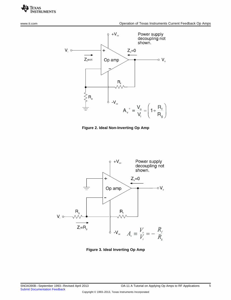
The two ideal op amp circuits assume that the source is coming from a ground referenced, zeroimpedance voltage source while their outputs are intended to act as ideal (zero ohm output impedance)voltage sources to a ground referenced load. The non-inverting configuration ideally presents an infiniteinput impedance, a zero ohm output impedance, and a voltage gain, as shown in Figure 2, from the plusinput to the output pin.
The ideal inverting op amp differs in several respects from the non-inverting. The output voltage is ideally180° out of phase from the input, which accounts for the signal inversion. The op amp’s (-) input ideallypresents a virtual ground, while drawing minimal current, for either voltage or current feedback op amps.This leaves Rg as the ideal input impedance seen by the source, while the voltage gain from the input ofRg to the output is simply -Rf/Rg. This signal inversion is usually of no consequence in an RF application,and most of this discussion will deal only with the magnitude of the inverting gain.
4 OA-11 A Tutorial on Applying Op Amps to RF Applications SNOA390B–September 1993–Revised April 2013Submit Documentation Feedback
Copyright © 1993–2013, Texas Instruments Incorporated
www.ti.com Operation of Texas Instruments Current Feedback Op Amps
Figure 2. Ideal Non-Inverting Op Amp
Figure 3. Ideal Inverting Op Amp
5SNOA390B–September 1993–Revised April 2013 OA-11 A Tutorial on Applying Op Amps to RF ApplicationsSubmit Documentation Feedback
Copyright © 1993–2013, Texas Instruments Incorporated

Operation of Texas Instruments Current Feedback Op Amps www.ti.com
When using op amps as RF amplifiers, we must first satisfy the I/O impedance matching requirements,recast the gain from a voltage gain to a power gain (in dB), and possibly configure for operation from asingle power supply. Figure 4 and Figure 5 show the op amps of Figure 2 and Figure 3 set up to provideI/O impedance matching with the resulting power gain equations, but still using bipolar supplies. Thebipolar power supplies allow operation to be maintained all the way down to DC. Single supply operationis possible and will be considered next
For the non-inverting case, setting Zi = 50Ω simply requires a 50Ω termination resistor to ground on thenon-inverting input, RT . Getting Zo = 50Ω simply requires a series 50Ω resistor in the output, RO.
For the inverting mode of op amp operation, the (+) input is ground referenced, while the signal channelinput impedance becomes the parallel combination of Rgand RM . As OA-13 Current Feedback Loop GainAnalysis and Performance Enhancement Application Report (SNOA366) describes, the current feedbacktopology depends on the value of the feedback resistor to determine the frequency response. With eachparticular op amp calling out a particular optimum Rf , Rg can then be used to set the gain and RM, alongwith Rg, will set the input impedance. Setting Rg to yield the desired gain and then setting RM to satisfy Zi =50Ω will work until the required Rg < 50Ω. Having fixed Rf to satisfy the amplifier’s stability requirements,going to higher and higher inverting gains will eventually yield Rg’s < 50Ω. Non-inverting operation shouldbe used if this limitation is reached. Rf can, however, be increased beyond the recommended value for acurrent feedback op amp in order to allow an Rg = 50 at higher gains, but only at the expense ofdecreasing bandwidth.
Figure 4. Non-Inverting Op Amp Configured for RF Application
6 OA-11 A Tutorial on Applying Op Amps to RF Applications SNOA390B–September 1993–Revised April 2013Submit Documentation Feedback
Copyright © 1993–2013, Texas Instruments Incorporated

www.ti.com Operation of Texas Instruments Current Feedback Op Amps
Figure 5. Inverting Op Amp Configured for RF Application
Note that for both topologies the gain to the matched load has been cut in half (-6dB), from the earlierideal case, through the voltage divider action of RO = RL . It is a simple, but critical, conversion from anydescription of output voltage swing to and from a power (in dBm) defined at the load. Figure 6 showsthese conversions for a purely sinusoidal signal. Basically, for whatever initial description of voltage swinggiven, we need to convert that into an RMS voltage, square it and divide by the load (RL = 50Ω normally)to get the absolute power in watts. This is then divided by 0.001 to reference that power to 1mW and 10 ×log of that expression is taken to yield the power in dBm.
7SNOA390B–September 1993–Revised April 2013 OA-11 A Tutorial on Applying Op Amps to RF ApplicationsSubmit Documentation Feedback
Copyright © 1993–2013, Texas Instruments Incorporated

Operation of Texas Instruments Current Feedback Op Amps www.ti.com
Figure 6. Converting Between Voltage Swings and Power
Every op amp has a specified maximum output voltage swing that is generally shown as a peak excursionfrom ground. This type of specification, for balanced bipolar power supplies, is really inferring how closethe output may come to the supply voltages before non-linear limiting occurs. For AC coupled RFapplications, it is always best to hold the output pin DC level centered between the two supply pins inorder to provide the maximum output Vpp . For more details on input and output voltage rangeconsiderations, see OA-15 Frequent Faux Pas in Applying Wideband Current Feedback AmplifiersApplication Report (SNOA367).
Most of Texas Instruments op amps do not require a ground reference for proper operation and can beeasily operated from a single supply. Generally, all that is required is to keep the DC voltage on the (+)input and the output pin centered between the voltages appearing on the two supply pins. For a singlesupply operation (with one supply pin held at ground) this translates into the (+) input and VO being held atVcc /2. For those amplifiers requiring a ground pin, that pin should also be driven with a low sourceimpedance voltage midway between the supply pins.
There are many possible implementations of single power supply op amp operation. Figure 7 and Figure 8show two simple ways to operate non-inverting and inverting op amps as AC coupled RF amplifiers usinga single power supply.
In the non-inverting case, the input termination is still DC coupled, while the (+) input bias is set by the twoRb ’s to yield Vcc /2. Rb should be large enough to limit excessive quiescent current in the bias path, butnot so large as to generate excessive DC errors due to the amplifier’s input bias current. The gain settingresistor, Rg , is also AC coupled to limit the DC gain to 1. Hence, the (+) input DC bias voltage alsoappears at the output pin. The output should be AC coupled in both circuits to limit the DC current thatwould be required if a grounded load were driven.
Single Supply, Non-Inverting Op Amp Operation For the single supply inverting amplifier of Figure 8, westill require the midpoint reference to be brought in on the (+) input. A de-coupling capacitor on that nodeis also suggested to decrease the AC source impedance for the non-inverting input noise current. Thegain for this non-inverting input reference voltage is again AC coupled to yield a unity DC gain to get Vcc/2at the output pin. The inverting input impedance goes from RM at DC to 50Ω at higher frequencies. RM, aswell as RT in Figure 7, could also be AC coupled to avoid DC loading on the source.
For both of these single supply circuits, we have given up the DC coupling for the signal path. The lowfrequency limits to operation will now be set by the AC coupling capacitors, along with impedances in eachpart of the circuit. All of the subsequent discussions assume balanced bipolar supplies, but apply equallyas well to single supply operation.
8 OA-11 A Tutorial on Applying Op Amps to RF Applications SNOA390B–September 1993–Revised April 2013Submit Documentation Feedback
Copyright © 1993–2013, Texas Instruments Incorporated

www.ti.com Operation of Texas Instruments Current Feedback Op Amps
Figure 7. Single Supply, Non-Inverting Op Amp Operation
Figure 8. Single Supply, Inverting Op Amp Operation
9SNOA390B–September 1993–Revised April 2013 OA-11 A Tutorial on Applying Op Amps to RF ApplicationsSubmit Documentation Feedback
Copyright © 1993–2013, Texas Instruments Incorporated

Small Signal AC Performance Characteristics www.ti.com
3 Small Signal AC Performance Characteristics
All of the typical small signal AC parameters specified for RF amplifiers are derived from the S-parameters(reference [1]). These are:
Scattering Parameters RF Amplifier Specification
S11 Input reflection Input VSWR
S22 Output reflection Output VSWR
S21 Forward transmission Amplifier gain and bandwidth
S12 Reverse transmission Reverse isolation
These frequency dependent specifications are measured using a network analyzer and an S-parametertest set. A full 2-port calibration should be performed prior to any device measurements. The HP8753A,used for the measurements reported here, incorporates full 12 term error correction in its 2-portcalibration. This basically normalizes all measurement errors due to imperfections in the cabling and testhardware (reference [2]).
Figure 9 and Figure 10 show the two configurations for the CLC404 used in demonstrating the smallsignal AC performance parameters listed above. In each case, the S-parameter test set places the deviceinto a 50Ω input and output environment. Both configurations achieve a voltage gain of 6 to the output pinand 3 to the 50Ω load. This yields a gain of 20 × Iog(3) = 9.54dB measured by the network analyzer.Recall that one of the advantages to using op amps in RF applications is the exceptional flexibility insetting the gain. A wide range of gains could have been selected for the test circuits of Figure 9. andFigure 10. ±6 was selected to allow easy comparisons to the CLC404’s data sheet specifications, whichare all defined at a gain of +6.
For the inverting gain configuration, RM along with Rg sets the input impedance to 50Ω. An RT of 50Ω isretained on the non-inverting input to limit the possibility of self-oscillation in the non-inverting inputtransistors (see OA-15 Frequent Faux Pas in Applying Wideband Current Feedback Amplifiers ApplicationReport (SNOA367).
Figure 9. Non-Inverting Amplifier S-parameter Test Circuit
10 OA-11 A Tutorial on Applying Op Amps to RF Applications SNOA390B–September 1993–Revised April 2013Submit Documentation Feedback
Copyright © 1993–2013, Texas Instruments Incorporated

www.ti.com Input/Output VSWR
Figure 10. Inverting Amplifier S-parameter Test Circuit
4 Input/Output VSWR
The Voltage Standing Wave Ratio (VSWR) is a measure of how well the input and output impedances arematched to the source impedance. (It is assumed throughout that the transmission line characteristicimpedance is also equal to the source impedance of both ports-50Ω in this case). It is desirable that theinput and output impedances be as closely matched as possible to the source for maximum powertransfer and minimum reflections.
(1)
Ideal, VSWR = 1
Typically, VSWR = 1.5, for RF-amps over their operating frequency range
Measuring the input VSWR is simply a matter of measuring the ratio of the reflected power vs. incidentpower on Port 1 of Figure 9 and Figure 10 (S11). A perfect match will reflect no power. Output VSWR ismeasured similarly at Port 2 (S22).
As described earlier, an op amp’s input and output impedances are determined by external componentsselected by the designer. For this reason, I/O VSWR is never shown on an op amp’s data sheet. ExcellentVSWR can, nevertheless, be achieved using the components shown in Figure 4 and Figure 5.
11SNOA390B–September 1993–Revised April 2013 OA-11 A Tutorial on Applying Op Amps to RF ApplicationsSubmit Documentation Feedback
Copyright © 1993–2013, Texas Instruments Incorporated

Input/Output VSWR www.ti.com
An op amp’s gain polarity has minimal effect on the output VSWR. At low frequencies, RO by itself willdetermine the output VSWR. Setting this resistor to 50Ω will yield excellent output VSWR to reasonablyhigh frequencies. As the test frequency increases, however, the op amp’s output impedance will begin toincrease as the loop gain rolls off (reference [3], page 237). This inductive characteristic can be partiallycompensated by a small shunt capacitance across R O. Figure 11 shows this, for either gain polarity, alongwith tested output VSWR with and without this shunt capacitance. The value of this capacitance willdepend on the amplifier and, to some extent, on the gain setting, and was determined empirically for thistest by using a small adjustable cap (5-20pF) directly across RO.
Figure 11. Measuring and Tuning CLC404 Output VSWR
The marker at 200MHz indicates an output VSWR of 1.3:1 when CT is tuned optimally. Tuning CT alsoextends the frequency response (S21) lightly and will be left in place for the remainder of the tests.
The input impedance match of the non-inverting topology Figure 9 is principally set by RT . As thefrequency increases, the input capacitance of the op amp will eventually degrade the input VSWR. Thiseffect is so negligible over the expected operating frequency range, however, that no tuning is required.
The input impedance match of the inverting topology Figure 10 is, at low frequencies, set by the parallelcombination of Rg and RM . This holds very well as long as the amplifier’s inverting input acts like a lowimpedance over frequency. For current feedback amplifiers, the inverting input is actually a driven, lowimpedance buffer. It’s impedance will, however, increase with frequency. A voltage feedback amplifier’sapparent inverting input impedance will also increase with frequency as its loop gain rolls off. In thevoltage feedback case, the increase in inverting input impedance will be seen at a lower frequency thanfor a current feedback amplifier and will depend strongly on the amplifier gain setting.
Figure 12 shows the tested input VSWR for the two gain polarities of Figure 9 and Figure 10. In this case,we are measuring S11 and allowing the HP8753A to convert the measurement and display VSWR directly.
12 OA-11 A Tutorial on Applying Op Amps to RF Applications SNOA390B–September 1993–Revised April 2013Submit Documentation Feedback
Copyright © 1993–2013, Texas Instruments Incorporated

www.ti.com Forward Gain and Bandwidth
Figure 12. CLC404 Input VSWR
Note carefully the change in scale for the input VSWR vs. the output VSWR plot. The marker on the non-inverting test trace shows an exceptional input VSWR of 1.03:1 at 200MHz, while the inverting, thoughhigher, remains under 1.4:1 through this range.
5 Forward Gain and Bandwidth
Typical RF amplifier specifications show a fixed gain, as defined in Figure 1, with a specified frequencyrange for 0.5dB gain flatness, along with -3dB cutoff frequencies. For the designer using a currentfeedback op amp, a wide range of possible gains are easily obtainable. With the CLC404’s specifiedvoltage gain range of ±1 to ±10, and including the additional 6dB loss from the output to the load, -6dB to14dB gains may be achieved using the CLC404. Higher gains can be achieved with this, or any othercurrent feedback amplifier, with some sacrifice in bandwidth (see OA-13 Current Feedback Loop GainAnalysis and Performance Enhancement Application Report (SNOA366)). For example, the CLC401,specified over a ±7 to ±50 voltage gain range, translates into an 11dB to 28dB gain range for RFapplications.
The forward gain over frequency (commonly called the frequency response and measured as S21) alwaysappear in the Texas Instruments data sheets over a range of gains. Small signal -3dB bandwidth and gainflatness are also guaranteed at a particular gain for each amplifier. Rarely does a voltage feedback opamp show the S21 characteristics, since it so strongly depends upon the gain setting. Rather, theseamplifiers show an open loop gain and phase plot and leave it to the designer to predict closed loop gainand phase. The frequency response plots for the Texas Instruments op amps are normalized to showeach gain coming in at the same grid on the plot for easier comparisons of frequency response shapeover a wide range of gains. Another advantage of the excellent loop gain control of the current feedbacktopology is exceptional forward gain phase linearity. This phase is also shown on the frequency responseplot. A maximum deviation from linear phase is guaranteed at a particular gain setting in the data sheetspecifications.
13SNOA390B–September 1993–Revised April 2013 OA-11 A Tutorial on Applying Op Amps to RF ApplicationsSubmit Documentation Feedback
Copyright © 1993–2013, Texas Instruments Incorporated

Forward Gain and Bandwidth www.ti.com
The part to part variation in the frequency response is minimal for the hybrid amplifiers from TexasInstruments, with more variation seen for the monolithic op amps. As Application Report OA-13(SNOA366) describes, the current feedback topology allows an easy, resistive trim for the frequencyresponse shape that has no impact on the forward gain. This frequency response flatness trim has thesame effect for either non-inverting or inverting topologies. Figure 13 shows this adjustment added to thecircuit of Figure 9, along with the measured S21 with and without this trim. As Application Report OA-13(SNOA366) describes, this resistive trim inside the feedback loop has the effect of adjusting the loop gain,and hence the frequency response, without adjusting the signal gain, which would still be set by only Rf
and Rg . This particular test achieved a flatness of ±.1dB from DC to 110MHz at a gain of 9.54dB for thenon-inverting test circuit shown (with identical results for an inverting configuration).
Figure 13. Measuring and Adjusting the Frequency Response S21
Note that the values for Rf and Rg have been reduced from those used in the circuit of Figure 9, althoughtheir ratio and hence the gain, have remained the same. With the adjustment pot set to zero ohms, thislower Rf value ensures that the frequency response will be peaked for any particular CLC404 used in thecircuit. Then, by increasing the resistance into the inverting input, the amplifier can be compensated andS21 adjusted to the excellent flatness shown above.
The part to part variation in frequency response becomes more pronounced as the desired operatingfrequencies and signal gains increase. Operation of the CLC404 through 50MHz at 9.54dB gain would, forexample, have minimal variation relative to operation through 100MHz and 14dB gain. For ±.1dB flatness,and considering the rapid degradation in distortion performance at higher frequencies, 100MHz is probablya reasonable upper limit for the operation of Texas Instruments op amps (available at the time ofpublication) in RF (or IF) applications. Higher frequency operation can be achieved if the degradedflatness and distortion characteristics are acceptable to the application. New product introductions can beexpected to extend this operating frequency.
14 OA-11 A Tutorial on Applying Op Amps to RF Applications SNOA390B–September 1993–Revised April 2013Submit Documentation Feedback
Copyright © 1993–2013, Texas Instruments Incorporated

www.ti.com Reverse Isolation
6 Reverse Isolation
This small signal AC characteristic is a measure of how much signal injected into the output port makes itback into the input source. The magnitude of S12 is the measure of reverse isolation. Texas Instrumentscurrent feedback op amps exhibit excellent reverse isolation relative to most RF amplifiers. This resultsfrom both the output and inverting input being driven, low impedance, nodes. To the extent that the outputof the op amp and its inverting input both present very low impedances over wide frequency ranges,significant signal attenuation can be expected in taking a signal voltage applied to the output matchingresistor and tracing it back to either an inverting or non-inverting input signal. Slightly more attenuation canbe expected for the non-inverting vs. inverting configurations, since the signal must also get from theinverting to non-inverting pin in the non-inverting case.
The circuit of Figure 13, along with the inverting circuit of Figure 14 were used to measure the reverseisolation for both gain polarities, as shown in Figure 15. Although reverse isolation is generally specifiedas a positive number, this is simply the negative of the log gain in going backwards through the amplifier.Hence, the plot of Figure 14 shows a rising “gain” that would be interpreted as a decreasing reverseisolation as we go to higher frequencies. As Figure 15 shows, isolations in excess of 30dB are easilyobtainable through frequencies far higher than the operating frequency range, with very high isolationsobserved at low frequencies.
Figure 14. Inverting Reverse Isolation Test Circuit
15SNOA390B–September 1993–Revised April 2013 OA-11 A Tutorial on Applying Op Amps to RF ApplicationsSubmit Documentation Feedback
Copyright © 1993–2013, Texas Instruments Incorporated

Dynamic Range Limiting Characteristics www.ti.com
Figure 15. Reverse Gain for the Circuits of Figure 13 and Figure 14
7 Dynamic Range Limiting Characteristics
The final area of concern in applying op amps to RF applications are the limits to dynamic range familiarto RF amplifier users. These are generally limited to:
• -1dB Compression Point
• 2-Tone, 3rd Order, Intermodulation Intercept
• Noise Figure
The -1dB Compression Point is a measure of the maximum output power capability of the amplifier. The 2-Tone Intercept allows the prediction of spurious signals caused by amplifier non-linearities when two inputsignals closely spaced in frequency are applied to the input. The noise figure is a measure of how muchnoise is added by the amplifier and will set a limit to the minimum detectable signal.
Although each of these can certainly be measured for any particular op amp configuration, theirinterpretation for op amps may vary from RF amplifiers depending on the op amp being used and thespecification. Each of these will be described generally and developed, and/or measured, for the CLC404with any anomalies in interpretation noted.
16 OA-11 A Tutorial on Applying Op Amps to RF Applications SNOA390B–September 1993–Revised April 2013Submit Documentation Feedback
Copyright © 1993–2013, Texas Instruments Incorporated

www.ti.com -1dB Compression Point
8 -1dB Compression Point
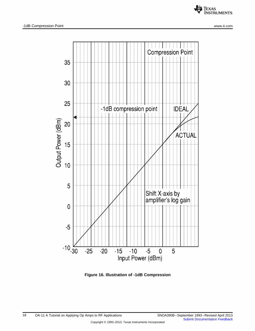
Briefly stated, this is the expected output power, at a fixed input frequency, where the amplifier’s actualoutput power is 1dBm less than expected. As Figure 16 shows, it can also be interpreted as the idealoutput power at which the actual amplifier gain has been reduced by 1dB from its value at lower outputpowers. With both the X and Y axis of Figure 16 a dBm scale, the output power vs. the input power willhave a slope of 1. If we shift the X-axis by the amplifier’s low power gain (a 20dB gain was used arbitrarilyin Figure 16), the amplifier’s input to output transfer would ideally be a unity slope line through the origin.
An additional interpretation of Figure 16 is that beyond the -1dB compression point the output powerremains fixed as the input power is increased. If S21 were measured at a fixed frequency, with a sweptinput power, we would get a horizontal line, showing the low power gain, that eventually transitions to a -1slope line as the output power becomes fixed while the input power continues to increase.
The -1dB compression power is commonly used as a maximum output power limit when computing anamplifier’s dynamic range. Standard AC coupled RF amplifiers show a relatively constant -1dBcompression power over their operating frequency range.
For an operational amplifier, the maximum output power depends strongly on the input frequency. The twoop amp specifications that serve a similar purpose to -1dB compression are output voltage range and slewrate. At low frequencies, increasing the power of a fixed frequency input will eventually drive the output“into the rails” - a saturation limit typically some number of diode drops below the supply voltages. Inaddition, as the input frequency increases, all op amps will reach a limit on how fast the output cantransition. This is typically specified as a slew rate indicating the maximum dV/dT at the output pin voltage.Half this slew rate is available at the matched load when an output series matching resistor is used. For asinusoidal signal, the maximum slew rate occurs at the 0 crossing. This maximum dV/dT is simply thepeak voltage exertion times the radian frequency. Given a slew rate in Volts/sec (SR) and a frequency, themaximum peak amplitude before slew limited operation is experienced is predicted to be SR/(2 × π ×frequency). However, this peak amplitude, which can be converted to a dBm power at the load using theexpressions developed earlier, does not relate directly to the measured -1dB compression.
17SNOA390B–September 1993–Revised April 2013 OA-11 A Tutorial on Applying Op Amps to RF ApplicationsSubmit Documentation Feedback
Copyright © 1993–2013, Texas Instruments Incorporated
-1dB Compression Point www.ti.com
Figure 16. Illustration of -1dB Compression
18 OA-11 A Tutorial on Applying Op Amps to RF Applications SNOA390B–September 1993–Revised April 2013Submit Documentation Feedback
Copyright © 1993–2013, Texas Instruments Incorporated
www.ti.com -1dB Compression Point
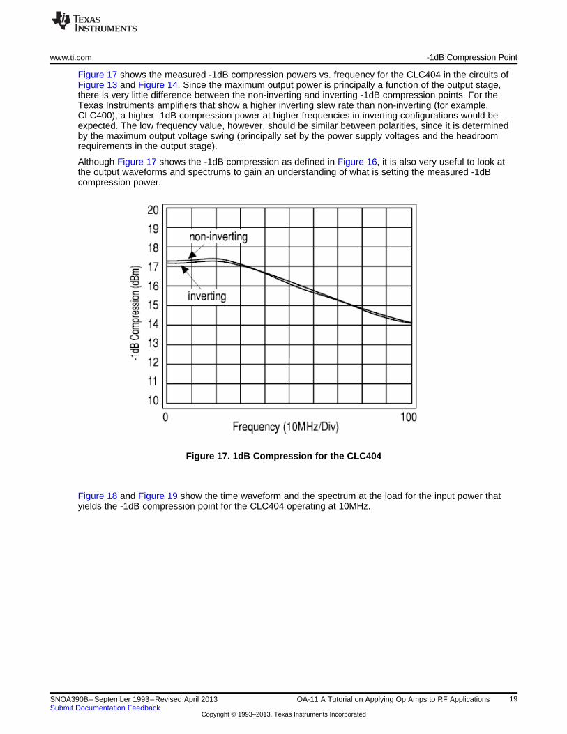
Figure 17 shows the measured -1dB compression powers vs. frequency for the CLC404 in the circuits ofFigure 13 and Figure 14. Since the maximum output power is principally a function of the output stage,there is very little difference between the non-inverting and inverting -1dB compression points. For theTexas Instruments amplifiers that show a higher inverting slew rate than non-inverting (for example,CLC400), a higher -1dB compression power at higher frequencies in inverting configurations would beexpected. The low frequency value, however, should be similar between polarities, since it is determinedby the maximum output voltage swing (principally set by the power supply voltages and the headroomrequirements in the output stage).
Although Figure 17 shows the -1dB compression as defined in Figure 16, it is also very useful to look atthe output waveforms and spectrums to gain an understanding of what is setting the measured -1dBcompression power.
Figure 17. 1dB Compression for the CLC404
Figure 18 and Figure 19 show the time waveform and the spectrum at the load for the input power thatyields the -1dB compression point for the CLC404 operating at 10MHz.
19SNOA390B–September 1993–Revised April 2013 OA-11 A Tutorial on Applying Op Amps to RF ApplicationsSubmit Documentation Feedback
Copyright © 1993–2013, Texas Instruments Incorporated

-1dB Compression Point www.ti.com
Figure 18. Output Waveform at 10MHz - 1dB Compression
Figure 19. Output Spectrum at 10MHz - 1dB Compression
20 OA-11 A Tutorial on Applying Op Amps to RF Applications SNOA390B–September 1993–Revised April 2013Submit Documentation Feedback
Copyright © 1993–2013, Texas Instruments Incorporated

www.ti.com -1dB Compression Point
At this low frequency, we are clearly running into an output voltage swing limitation. With a 17.3dBm -1dBcompression (as shown at 10MHz in Figure 17), we would expect the fundamental amplitude in thespectrum to be at 16.3dBm. The observed 16dBm in the spectrum of Figure 19 is a reasonable match tothis expected fundamental power. It is, however, incorrect to directly convert this fundamental power at -1dB compression into a sinusoid and expect that the amplifier can deliver a sinusoid of this amplitude. Forthe 16.3dBm fundamental power predicted by the -1dB compression measurement, we might expect thatthe output is delivering an approximately 4Vpp sinusoidal swing at the load, or ±4V swing at the output pin.Although this would exceed the maximum output swing specification for the CLC404 operating at ±5 voltsupplies, this amplitude of sinusoid is in fact available if a zero loss filter is used to pass on only thefundamental harmonic.
Notice that a considerable portion of the output power has been spread into the odd order harmonics. Thisis typical of the square wave output observed in the time domain trace of Figure 18. The fundamental(10MHz) power can be related to the output time waveform amplitude through the Fourier seriesexpansion of the output waveform. If the output were a perfect square wave, under conditions of outputvoltage limited operation, a peak square wave amplitude of A would generate a fundamental frequencyamplitude of 4 × A/π. Going from the measured peak amplitude of the output time waveform, theanticipated -1dB compression would be calculated as the power in a sinusoid 4/π times the square waveamplitude +1dBm. Doing this for the measured ±1.8V swing of Figure 18 would predict 15.1dBm (peak-peak square wave amplitude converted to dBm) + 2.1dBm (20 × Iog(4/π)) + 1dBm (reported -1dBm outputpower is 1dBm higher than measured power) = 18.3dBm. This is 1dBm higher than measured. This canbe explained by the less than perfect square wave shape shown in the time waveform of Figure 18. Thisless than perfect square wave will yield a coefficient for the fundamental term in the Fourier expansion thatis actually less than the predicted A × 4/π.
As the operating frequency increases, the slew limit for the op amp will eventually restrict the achievableoutput swing to something less than the output voltage swing limit of the amplifier. This can be observedin Figure 11 at approximately 30MHz for the CLC404. Again, it is instructive to look at the time waveformand resulting spectrum when operating at an input power that yielded a -1dB compression in measuredgain at the these higher frequencies. Figure 20 and Figure 21 show this for the non-inverting circuit(Figure 13) operating at the input power necessary to produce the measured -1dB compression with a50MHz sinusoidal input signal (from Figure 17, this input power would be 16.3dBm - 9.54 (gain) =6.8dBm)
The measured -1dB compression power under slew limited conditions is dependent on the amount ofpower in the fundamental frequency generated by the time waveform shown in Figure 20. Although wecan say that the -1dB compression must be related to the amplifier’s slew rate, it would be very difficult torelate the slew rate to the waveform shape and then, through the Fourier series, to the fundamental powerand hence -1dB compression. The exact distribution of power into the fundamental and harmonics ischanging over frequency. All that can really be said is that at these higher frequency -1dB compressions,a significantly distorted waveform with a peak to peak excursion less than that seen at lower frequenciesis being generated.
At low frequencies, the -1dB compression power can be predicted approximately using the analysis shownearlier by assuming a square wave output set by the output voltage swing limits shown in the op amp datasheet. Remember that the output voltage range specified in the data sheet is twice what can be deliveredthrough the 6dB loss taken from the matching resistor to the load. It is not, however, possible to easilypredict the higher frequency -1dB compression from the slew rate specification. As will become apparentin the next section, it is also not possible to relate the -1dB compression to the third order intercept.Typical RF amplifiers will show a 3rd order intercept 10dBm higher than the -1dB compression point.Texas Instruments op amps, if they show an intercept characteristic, have an intercept considerably higherthan what would be predicted by adding 10dBm to the -1dB compression.
21SNOA390B–September 1993–Revised April 2013 OA-11 A Tutorial on Applying Op Amps to RF ApplicationsSubmit Documentation Feedback
Copyright © 1993–2013, Texas Instruments Incorporated

-1dB Compression Point www.ti.com
Figure 20. Measured Output Waveform at 50MHz -1dB Compression
Figure 21. Measured Output Spectrum at 50MHz -1dB Compression
22 OA-11 A Tutorial on Applying Op Amps to RF Applications SNOA390B–September 1993–Revised April 2013Submit Documentation Feedback
Copyright © 1993–2013, Texas Instruments Incorporated

www.ti.com 2-Tone, 3rd Order Intermodulation Intercept
9 2-Tone, 3rd Order Intermodulation Intercept
This specification is directed at predicting the 3rd order intermodulation distortion powers for anycombination of two closely spaced (in frequency) input signals. Any amplifier can be modeled to have apolynomial approximation to its transfer function from input to output. When two input signal frequenciesare present, the 3rd order term of this polynomial approximation will give rise to distortion terms atfrequencies that can be very near the input signal frequencies. These closely spaced distortions areconsiderably more troublesome to narrowband IF channels than the simple harmonic distortion terms thatappear in integer increments away from the input signal frequency.
Appendix B expands all of the spurious frequency locations and distortion coefficients for two input signalsat frequencies of fO-Δf and fO+Δf when passed through a 5th order polynomial. With this simple definitionof equal deviations from a center frequency (an average frequency), all of the spurious frequencylocations become very simple algebraic expressions of fO and Δf. Using this approach to defining the testfrequency locations also allows a clear illustration of the symmetric clusters of spurious terms aroundinteger multiples of fO. From Appendix B, the 3rd order inter-modulation terms fall at fO ± ΔDfO. With aninput signal defined as Vi = Acos(2Δ(fO - Δf)t) + Bcos(2Δ(fO + Δf)t), and an input to output voltage gaintransfer function of VO = K0 + K1 Vi + K2Vi
2 + K3Vi3 (ignoring the higher order terms for now), a lower 3rd
order spurious term at fO - 3Δf with an amplitude of (3/4) × K3 × A × B2 and an upper spurious at fO + 3Δfwith an amplitude of (3/4) × K3 × A2 × B will result.
If equal amplitude signals were applied to the input (A = B), and if these were increased in an equalfashion, the two spurious amplitudes would increase in a cubic fashion. In dBm terms, if the two input, andhence output, powers were increased by 1dBm, this model predicts that the two output third orderspurious powers will increase by 3dBm. It is interesting to note the effect of adjusting just one of the inputfrequency power’s. Changing the lower test frequency power by 1dBm will change the lower spurious by1dBm and the upper spurious by 2dBm. Conversely, changing the upper test frequency power by 1dBmwill change the lower spurious by 2dBm and the upper by 1dBm. The dependence of the 3rd orderspurious power to output test frequency power (assuming equal powers for each test frequency) is showngraphically in Figure 22.
As shown in Figure 22, the 3rd order spurious powers, increasing at a 3X rate vs. the input power, will, atsome output power, “intercept” the desired output powers that are increasing at a 1X rate vs. the inputpower. Another way of saying this is that there is a 2X closure rate between the desired output powersand the undesired 3rd order intermodulation spurious powers. The graph of Figure 22 was arbitrarily setup for an amplifier gain of 20dB (the x-axis has been shifted to yield 0dBm output power for -20dBm inputpower) and for a 30dBm 3rd order intercept. No actual amplifier will be able to reach the intercept pointfrom an output power standpoint since this intercept typically exceeds the -1dB compression power by atleast 10dBm. The intercept is intended as a mathematical construct to allow the prediction of the spuriouspower level for a given output signal power. For an amplifier that shows a 3rd order intermodulationintercept characteristic, a single measurement of output powers and spurious levels are sufficient to solvefor the intercept point as shown by the equation in Figure 22.
23SNOA390B–September 1993–Revised April 2013 OA-11 A Tutorial on Applying Op Amps to RF ApplicationsSubmit Documentation Feedback
Copyright © 1993–2013, Texas Instruments Incorporated

2-Tone, 3rd Order Intermodulation Intercept www.ti.com
Figure 22. Output and 3rd Order Spurious Power vs. Input Power
24 OA-11 A Tutorial on Applying Op Amps to RF Applications SNOA390B–September 1993–Revised April 2013Submit Documentation Feedback
Copyright © 1993–2013, Texas Instruments Incorporated
www.ti.com 2-Tone, 3rd Order Intermodulation Intercept
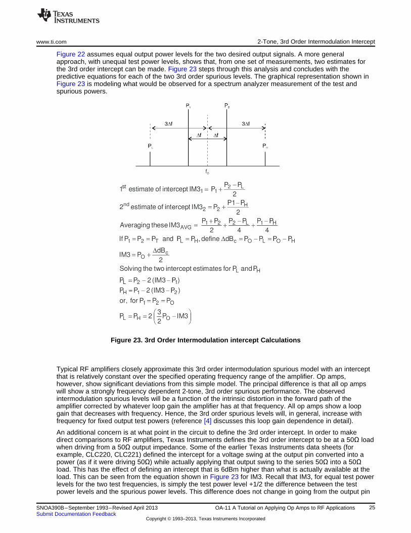
Figure 22 assumes equal output power levels for the two desired output signals. A more generalapproach, with unequal test power levels, shows that, from one set of measurements, two estimates forthe 3rd order intercept can be made. Figure 23 steps through this analysis and concludes with thepredictive equations for each of the two 3rd order spurious levels. The graphical representation shown inFigure 23 is modeling what would be observed for a spectrum analyzer measurement of the test andspurious powers.
Figure 23. 3rd Order Intermodulation intercept Calculations
Typical RF amplifiers closely approximate this 3rd order intermodulation spurious model with an interceptthat is relatively constant over the specified operating frequency range of the amplifier. Op amps,however, show significant deviations from this simple model. The principal difference is that all op ampswill show a strongly frequency dependent 2-tone, 3rd order spurious performance. The observedintermodulation spurious levels will be a function of the intrinsic distortion in the forward path of theamplifier corrected by whatever loop gain the amplifier has at that frequency. All op amps show a loopgain that decreases with frequency. Hence, the 3rd order spurious levels will, in general, increase withfrequency for fixed output test powers (reference [4] discusses this loop gain dependence in detail).
An additional concern is at what point in the circuit to define the 3rd order intercept. In order to makedirect comparisons to RF amplifiers, Texas Instruments defines the 3rd order intercept to be at a 50Ω loadwhen driving from a 50Ω output impedance. Some of the earlier Texas Instruments data sheets (forexample, CLC220, CLC221) defined the intercept for a voltage swing at the output pin converted into apower (as if it were driving 50Ω) while actually applying that output swing to the series 50Ω into a 50Ωload. This has the effect of defining an intercept that is 6dBm higher than what is actually available at theload. This can be seen from the equation shown in Figure 23 for IM3. Recall that IM3, for equal test powerlevels for the two test frequencies, is simply the test power level +1/2 the difference between the testpower levels and the spurious power levels. This difference does not change in going from the output pin
25SNOA390B–September 1993–Revised April 2013 OA-11 A Tutorial on Applying Op Amps to RF ApplicationsSubmit Documentation Feedback
Copyright © 1993–2013, Texas Instruments Incorporated

2-Tone, 3rd Order Intermodulation Intercept www.ti.com
to the matched load. However, the output voltage swing will drop by 6dB and, since the output pin powerwas erroneously defined as being a particular voltage swing across a 50Ω load (when it in fact sees a100Ω load), this will translate into a 6dBm drop in the test power level to the matched 50Ω load.Therefore, the usable intercept at the matched load is 6dBm lower than specified in those earlier datasheets that call for an output power calculation at the output pin.
Given that the test power level is being defined at the matched load, it is important to consider theamplifier limitations on the maximum power and frequency of test. For a two tone test of equal powers andclosely spaced frequencies, the available peak to peak voltage swing for each test frequency at the load is1/4 the peak to peak output voltage available at the amplifier’s output pin while the available slew rate foreach test tone can be estimated as 1/8 the amplifier’s specified slew rate. For a 2-tone test signal beinggenerated at a matched load, twice the peak to peak swing is being generated in the envelope (and twicethe slew rate). Going back through the matching resistor to the output pin will double this swing and slewrate again. In addition, empirical testing has revealed that an overall maximum slew rate at the output pinthat is 1/2 the specified op amp slew rate will show low spurious performance. As the slew rate of theoutput pin waveform exceeds this limit, additional non-linearities come into play rapidly increasing the 3rdorder spurious powers.
Using the circuit of Figure 13 and the typical specifications for the CLC404, the maximum test power levelat the load for each test tone, from an output swing standpoint, would be (1/4)*6Vpp = 1.5Vpp . Thistranslates into a maximum test power level for each tone of approximately 8dBm. At this maximum outputswing, the available slew rate of (1/8) × 2000Vμmsec = 250V/μsec will limit the frequency of operation toless than (SR/(2 × π × Vpp/2) = 250E6/(2 × π × .75V) = 53MHz. As the test or operation powers decrease,this upper frequency limit set by the slew rate limit will increase. For example, dropping the power 6dB to2dBm will push this limit out to 106MHz.
Although some of the Texas Instruments current feedback amplifiers (for example, CLC400, CLC401,CLC560) show a good approximation to the 3rd order intercept model, the CLC404, used in the examplecircuits shown thus far, shows a spurious power vs. test power characteristic that deviates significantlyfrom the simple model of Figure 22. Figure 24 shows the difference between the test and spurious powersplotted as a function of single tone test power at the load. Note that the independent variable axis is outputpower; not the input power shown in Figure 22. Ideally, this would, at each frequency, yield a straight linewith a slope of +2 (instead of the +3 slope shown in Figure 22). A similar plot for the CLC401, which moreclosely approximates this ideal, is shown in Figure 25. If an op amp closely approximated the 3rd orderintercept model, a single measurement at one operating power would be adequate to predict the interceptat that frequency.
The 3rd order spurious plot for the CLC404 is clearly showing some additional mechanism that is holdingthe spurious levels down as the output power level moves above 0dBm. At lower power levels, it appearsthat the spurious characteristic is moving towards a linear slope of 2 as predicted by the simple interceptmodel. Looking again at the 5th order expansion of the 2-tone coefficients shown in Appendix B, anadditional 5th order term contributes to the spurious powers observed at the 3rd order intermodulationfrequencies. Normally, it would be expected that the K5 coefficient is so much lower than the K3 value thatthis 5th order contribution can be neglected. However, in the case of the CLC404, the K3 coefficient is solow as to make this second term significant at higher operating powers. Note that the contribution of this5th order term increases as the 5th power of the two test powers vs. the more slowly increasing 3rd orderterm. It can be theorized that the 5th order coefficient is of opposite sign to the 3rd order coefficient. Then,as the test powers increase to the level that this 5th order term becomes significant in magnitude vs. the3rd order, the spurious levels actually decrease for increasing output power.
The projected intercept at very low power levels can still be used to predict the spurious free dynamicrange. In Figure 24, the intercept at low output powers may be estimated for a particular frequency as theoutput power minus 1/2 the y-axis value. However, it should be realized that wideband op amps like theCLC404 actually provide better spurious performance at high powers than would be predicted by this lowpower intercept model.
26 OA-11 A Tutorial on Applying Op Amps to RF Applications SNOA390B–September 1993–Revised April 2013Submit Documentation Feedback
Copyright © 1993–2013, Texas Instruments Incorporated

www.ti.com 2-Tone, 3rd Order Intermodulation Intercept
Figure 24. Measured 3rd Order Spurious for the CLC404
Figure 25. Measured 3rd Order Spurious for the CLC401
27SNOA390B–September 1993–Revised April 2013 OA-11 A Tutorial on Applying Op Amps to RF ApplicationsSubmit Documentation Feedback
Copyright © 1993–2013, Texas Instruments Incorporated

Noise Figure www.ti.com
The 3rd order intercept performance is typically very similar between inverting and non-invertingtopologies. As discussed in reference 4, anything that changes the loop gain of the op amp will have aneffect on the 3rd order spurious performance. Increasing loop gain, either by going to low feedbackresistor values for current feedback op amps or low signal gains for voltage feedback op amps, willdecrease the spurious powers. In both cases, however, increasing the loop gain by changing the externaloperating point is constrained by closed loop stability considerations. 3rd order distortions andintermodulations can be further reduced by operating any op amp at higher quiescent currents (if possible)and/or driving the output into a higher impedance load for those situations not requiring a 50Ω matchedimpedance environment.
10 Noise Figure
Unlike the compression point and 3rd order intermodulation intercept, the noise figure for an op amp isalways usable in the same way that it is for an RF amp. It is important to remember that, like compressionand intercept, a noise figure is generally developed at a particular frequency and may change overfrequency. Normally, however, a single value can be used above the op amp’s 1/f noise corner frequency(for an additional noise discussion and its appendices for 1/f noise corner discussion and tabulated opamp input noise terms for Texas Instruments op amps, see OA-12 Noise Analysis for Comlinear AmplifiersApplication Report (SNOA375)).
The noise figure can be accurately calculated from the equivalent input noise terms for an op amp and theresistor values used to achieve the desired gain and input impedance. Unlike an RF amplifier with a fixedgain and noise figure, an op amp’s noise figure will be strongly dependent on the gain setting. We can,however, easily predict the noise figure with the equations developed here.
A very general development for an op amp’s non-inverting noise figure will be performed in order to alloweasy comparison to noise figure expressions found in earlier Texas Instruments data sheets. The invertingop amp’s noise figure will, however, proceed with the assumption normally used – that the inputimpedance is to be matched to the source impedance.
An idealized schematic illustrating the definition of noise figure is shown in Figure 26.
Figure 26. Noise Figure Definition
28 OA-11 A Tutorial on Applying Op Amps to RF Applications SNOA390B–September 1993–Revised April 2013Submit Documentation Feedback
Copyright © 1993–2013, Texas Instruments Incorporated

www.ti.com Noise Figure
All of the input and output noise and signal terms in the equation for noise figure (NF) are considered tobe powers. Ni is the noise power delivered by the source resistor to the input of the amplifier. All othernoise sources are considered to be part of the amplifier and contribute to the noise power, No , seen at theoutput.
Looking at the two parts of the NF expression (inside the log function) yields:
Si /So = Inverse of the power gain provided by the amplifier
No /Ni = Total output noise power, including the contribution of R S , divided by the noise power at the inputdue to RS
To simplify this, consider Na as the noise power added by the amplifier (reflected to its input port):
Si/So = 1/G
No/Ni = G × (N i + N a )/N i (where G × (N i + N a ) = N o)
Substituting these two expressions into the NF expression:
(2)
The noise figure expression has simplified to depend only on the ratio of the noise power added by theamplifier at its input (considering the source resistor to be in place but noiseless in getting Na) to the noisepower delivered by the source resistor (considering all amplifier elements to be in place but noiseless ingetting Ni). Generally, the definition for NF also constrains the input impedance for the amplifier to beconjugate matched to the source resistor (this yields Ni = kT with this constraint). We will, however, relaxthis constraint initially to allow comparison to the NF expressions found in Texas Instruments earlier datasheets.
The NF of Equation 2 is specified in terms of a power ratio. The individual noise terms for the op amp are,however, expressed as spot noise voltages or currents (Spot means in a 1Hz bandwidth, as opposed tointegrated over some noise power bandwidth. See OA-12 Noise Analysis for Comlinear AmplifiersApplication Report (SNOA375)). Combining separately contributing noise sources is a matter of addingnoise powers. This can be done by converting all current noises to a voltage through the appropriateimpedance, then summing all of the squared noise voltage terms. Any impedance (normally needed todefine a power) or noise power bandwidth (used to convert from spot to integrated noise) will normalizeout since we are developing the ratio of two powers at the same point in the circuit. Getting to the totalspot noise power is then simply a matter of summing all the relevant squared noise voltages.
Figure 27 shows an op amp in the non-inverting configuration with all of the individual resistor andamplifier input noise terms detailed.
29SNOA390B–September 1993–Revised April 2013 OA-11 A Tutorial on Applying Op Amps to RF ApplicationsSubmit Documentation Feedback
Copyright © 1993–2013, Texas Instruments Incorporated

Noise Figure www.ti.com
Figure 27. Non-Inverting Op Amp Noise Figure Analysis Circuit
Recall that the noise of a resistor (Johnson Noise) can be defined as either a spot current or voltagenoise. For a resister of value R, these two possible expressions are:
(3)
where;
k = Boltzman’s constant
k = 1.38E-23 Joules/°Kelvin
T = °Kelvin = 290° in this analysis
4kT = 16E-21 Joules at T = 290°K
The 3 amplifier noise terms are available for most of Texas Instruments amplifiers in Application ReportOA-12 (SNOA375). If the spot noise figure below the 1/f noise corner is of interest, Application Report OA-12 also shows how to approximate the low frequency spot noise from the high frequency flat band valueand the 1/f noise corner frequency.
Using the circuit of Figure 27, the NF expression can be developed by generating an expression for Ni andNa . Ni is the noise power delivered by the source resistor noise to the input of the amplifier. This analysissimply proceeds by considering the noise voltages as sources in normal linear circuit analysis, buteventually squaring the resulting noise voltage delivered to RT from es. Figure 28 shows the equivalentcircuit and the resulting Ni . This is considering the amplifier to have an infinite non-inverting inputimpedance, with all other noise sources neglected for now (superposition of noise voltage contributionsare used throughout this analysis).
30 OA-11 A Tutorial on Applying Op Amps to RF Applications SNOA390B–September 1993–Revised April 2013Submit Documentation Feedback
Copyright © 1993–2013, Texas Instruments Incorporated

www.ti.com Noise Figure
Figure 28. Input Noise Power Calculation
To get an expression for Na , all other noise voltages and currents are referred to the non-inverting inputand summed as voltages squared. For the noise terms on the inverting side of the amplifier, it is best tofind each term’s gain to the output voltage, then reflect back to the non-inverting input by dividing by thenon-inverting voltage gain of the amplifier. At this point, since we are dealing with linear voltage gains,define this gain as Av + = 1 + Rf /Rg . Table 1 tabulates each individual voltage and current noise and its“gain” to the input of Figure 27. Note that all current noise terms have an impedance in their gainexpression to yield all voltage noise terms at the input of the amplifier.
Table 1. Noise Terms Contributing to Na for the Non-inverting Op Amp Configuration
Noise Source Value Voltage Gain to Input
Non-inverting input voltage noise en 1
Non-inverting input current noise ini Rn|| RT→ (RP)
Inverting input current noise ii Rf/Av+
Input terminating resistor voltage noise RS/RS+RT
Gain setting resistor current noise Rf/Av+
Feedback resistor voltage noise 1/Av+
One point of possible confusion is that, although we are trying to develop the total noise power at the inputof the op amp, what relation does this have to the input voltage noise term that already appears in the opamp model, en. As described in Application Report OA-12 (SNOA375), the noise model for an op ampattempts to lump all the internal noise sources of the actual amplifier into an equivalent input noise voltageat the non-inverting input and two input noise currents. The intent is to provide a means of predicting thenoise performance over a wide range of external operating conditions. The en shown in the analysis
31SNOA390B–September 1993–Revised April 2013 OA-11 A Tutorial on Applying Op Amps to RF ApplicationsSubmit Documentation Feedback
Copyright © 1993–2013, Texas Instruments Incorporated

Noise Figure www.ti.com
model of Figure 27 is associated only with the internal characteristics of the op amp itself. The totalamplifier output noise includes this and contributions from all of the other noise sources shown there.Having gotten to an expression for the total output noise voltage, an equivalent input noise voltage may bederived by simply dividing by the voltage gain of the op amp. This step of input referring each noisesource is performed for each term in Table 1.
To form an expression for Na, we need only to sum the squared product of each noise source and itsassociated gain, as shown in Table 1.
(4)
An expression for the non-inverting noise figure (N+) may now be derived by substituting the equation inFigure 28 and Equation 4 back into Equation 2.
(5)
Simplifying two of these terms:
(6)
32 OA-11 A Tutorial on Applying Op Amps to RF Applications SNOA390B–September 1993–Revised April 2013Submit Documentation Feedback
Copyright © 1993–2013, Texas Instruments Incorporated

www.ti.com Noise Figure
This expression for the non-inverting noise figure closely matches the equation shown in the CLC205 andCLC206 data sheets. Equation 6 differs only in some of the variable names and in the addition of a termdue to the Rf and Rg noise, which the CLC205 and CLC206 equations neglected.
33SNOA390B–September 1993–Revised April 2013 OA-11 A Tutorial on Applying Op Amps to RF ApplicationsSubmit Documentation Feedback
Copyright © 1993–2013, Texas Instruments Incorporated
Noise Figure www.ti.com
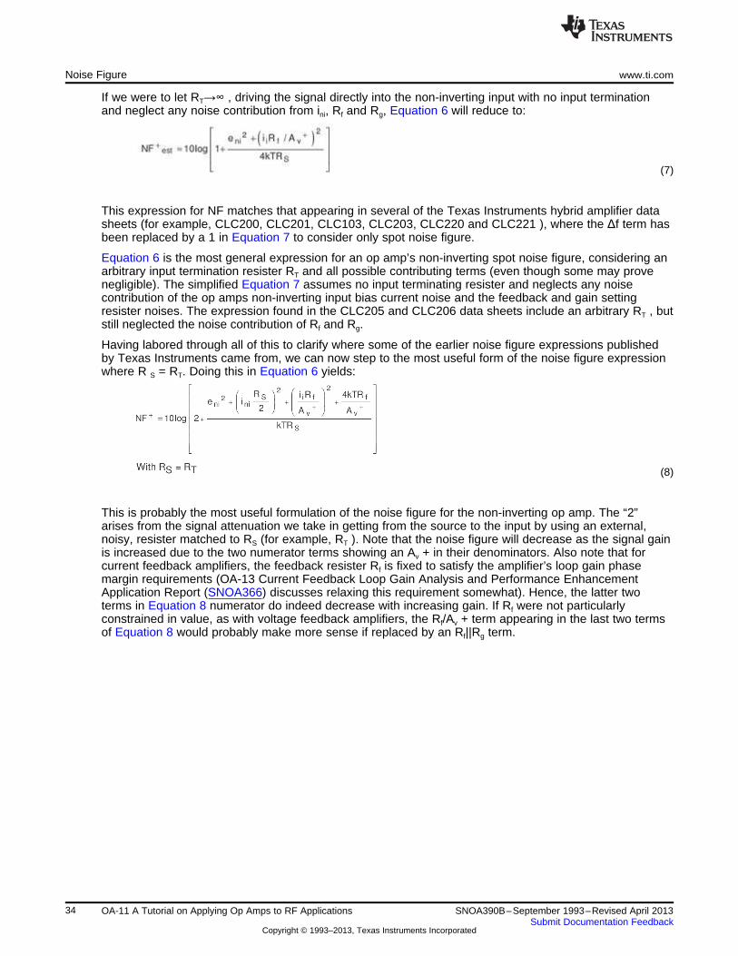
If we were to let RT→∞ , driving the signal directly into the non-inverting input with no input terminationand neglect any noise contribution from ini, Rf and Rg, Equation 6 will reduce to:
(7)
This expression for NF matches that appearing in several of the Texas Instruments hybrid amplifier datasheets (for example, CLC200, CLC201, CLC103, CLC203, CLC220 and CLC221 ), where the Δf term hasbeen replaced by a 1 in Equation 7 to consider only spot noise figure.
Equation 6 is the most general expression for an op amp’s non-inverting spot noise figure, considering anarbitrary input termination resister RT and all possible contributing terms (even though some may provenegligible). The simplified Equation 7 assumes no input terminating resister and neglects any noisecontribution of the op amps non-inverting input bias current noise and the feedback and gain settingresister noises. The expression found in the CLC205 and CLC206 data sheets include an arbitrary RT , butstill neglected the noise contribution of Rf and Rg.
Having labored through all of this to clarify where some of the earlier noise figure expressions publishedby Texas Instruments came from, we can now step to the most useful form of the noise figure expressionwhere R S = RT. Doing this in Equation 6 yields:
(8)
This is probably the most useful formulation of the noise figure for the non-inverting op amp. The “2”arises from the signal attenuation we take in getting from the source to the input by using an external,noisy, resister matched to RS (for example, RT ). Note that the noise figure will decrease as the signal gainis increased due to the two numerator terms showing an Av + in their denominators. Also note that forcurrent feedback amplifiers, the feedback resister Rf is fixed to satisfy the amplifier’s loop gain phasemargin requirements (OA-13 Current Feedback Loop Gain Analysis and Performance EnhancementApplication Report (SNOA366) discusses relaxing this requirement somewhat). Hence, the latter twoterms in Equation 8 numerator do indeed decrease with increasing gain. If Rf were not particularlyconstrained in value, as with voltage feedback amplifiers, the Rf/Av + term appearing in the last two termsof Equation 8 would probably make more sense if replaced by an Rf||Rg term.
34 OA-11 A Tutorial on Applying Op Amps to RF Applications SNOA390B–September 1993–Revised April 2013Submit Documentation Feedback
Copyright © 1993–2013, Texas Instruments Incorporated

www.ti.com Inverting Op Amp Noise Figure
11 Inverting Op Amp Noise Figure
In this case, the discussion will be simplified by constraining the input impedance of the op amp to beequal to RS. Figure 29 shows the circuit for analysis with all of the contributing noise sources:
RT has been retained on the non-inverting input, along with its noise voltage source, for completegenerality. Rg’s noise now appears as a voltage source instead of the current noise term used in the non-inverting analysis. Again, developing the noise figure expression for the inverting amplifier configuration issimply a matter of resolving Na and Ni and placing these expressions into Equation 2. Knowing that theinput impedance is matched to RS, 1/2 of the noise voltage attributed to RS will be delivered to the inputport of the amplifier. This yields a (voltage) 2 at the input.
Figure 29. Inverting Op Amp Noise Figure Analysis
(9)
Table 2 shows each individual noise terms, except es, with each term’s “gain” to the inverting input. Thenoise terms on the non-inverting input have a gain of At to the inverting input. This represents the non-inverting gain to the output divided by the inverting gain back to the inverting input. The two resistor noiseterms for RM and Rg are taken to have a voltage gain to the inverting input defined simply by the resistordivider networks and simplified with the constraint on RM that it is to be set to yield Rg||RM = RS . It is,perhaps, easiest to confirm the gain equations for Rg ’s and RM ’s noise by computing the current thosevoltages generate into Rg , taking this current to the output by multiplying by Rf and then reflecting back tothe inverting input by dividing by Av - = Rf /Rg . Doing this and then substituting in for RM , as shown inTable II, will (with some manipulation) yield the simple gain expressions found in Table II. The invertingnoise current and Rf noise voltage are taken to the output then reflected back to the inverting input bydividing by the inverting gain.
35SNOA390B–September 1993–Revised April 2013 OA-11 A Tutorial on Applying Op Amps to RF ApplicationsSubmit Documentation Feedback
Copyright © 1993–2013, Texas Instruments Incorporated

Inverting Op Amp Noise Figure www.ti.com
Table 2. Noise Terms Contributing to Na for the Inverting Op Amp Configuration
Noise Source Value Voltage Gain to Input
Non-inverting input voltage noise en AT
Non-inverting input current noise ini RTAT
Non-inverting input source resistor noise AT
Inverting input current noise ii
Inverting input impedance matching resistor noise
Gain setting resistor
Feedback resistor voltage noise
where:
(10)
The noise terms on the non-inverting side of the op amp have a gain of AT to the inverting input. As Av-
increases, this gain drops to < 1, which contributes to the lower noise figure achievable using the invertingamplifier configuration. Again, an expression for a noise (voltage) 2 at the input may be obtained by takingthe sum of the squared product of each noise source and associated gain shown in Table 2.
(11)
Combining the two noise powers attributed to the input matching network will allow considerablesimplification in the final inverting noise figure expression. Substituting in for RM with the expression shownas part of Table 2 and expanding the squared gain expressions.
(12)
36 OA-11 A Tutorial on Applying Op Amps to RF Applications SNOA390B–September 1993–Revised April 2013Submit Documentation Feedback
Copyright © 1993–2013, Texas Instruments Incorporated

www.ti.com Inverting Op Amp Noise Figure
Putting this back into the inverting ea2 expression and grouping the non-inverting input noise terms
together yields:
(13)
Putting the expressions for inverting ea2 and ei
2 (Equation 13 and Equation 14) back into the noise figureexpression (Equation 2), and recognizing that dividing each term by RS will yield Na and Ni respectively,shows that the kTRs term that arose in ea
2 from the RM and Rg resistor noises will collapse to a simpleterm, not including kTRs (very reminiscent of the “2” appearing in the NF+ expression). One difference isthat this part of the expression includes the contribution of both RM and Rg, while the non-invertingequation kept the Rg noise as part of the equivalent input noise. This arises since Rg is now constrained bythe input impedance matching requirement and can, therefore, be taken into this simplified form. Theinverting noise figure NF- is then:
(14)
To compare the non-inverting noise figure expression (Equation 9) to the inverting expressions(Equation 14), note that noise terms on the non-inverting input side have a gain of 1 for the non-invertingconfiguration but a gain of At for the inverting. Also note that the term associated with the feedbackresistor noise is divided by simply Av
+ in the non-inverting case. This arises because it also includes the Rg
noise in the non-inverting expression. However, it is divided by (Av-)2 in the inverting case. This arises from
the Rg noise term being considered part of the input termination. In this case, Rg and RM’s noise, appearsin 2 × (2 × Rg/Rs - 1) as part of the noise figure expression. Note that this collapses to simply equal 2when Rg = Rs similar to the NF+ case.
At low inverting gain, the non-inverting input noise terms have a larger impact for the invertingconfiguration than for an equivalent non-inverting gain, yielding a higher noise figure. As Av
-increases,however, the non-inverting noise terms will be attenuated in going to the inverting signal input referencepoint, yielding a lower inverting noise figure than for an equivalent gain non-inverting configuration.
Figure 30 compares the noise figures over gain for the non-inverting vs. inverting configurations using theCLC404. For this comparison, Rf is assumed fixed at 500Ω, RT for the non-inverting case = 50Ω; but is setto 25Ω for the inverting case. With these constraints, Rg and RM will be set by the desired gain and therequirement that Rg ||RM = RS in the inverting mode. RS is assumed = 50Ω throughout. The inverting noisefigure plot simply stops at the point where Rg = 50Ω, since higher gains are not possible (with a fixed Rf )while retaining the input impedance matching requirement. Also note that log gains are shown on the x-axis to the matched load, while the voltage gains used in the noise figure calculations are the linearvoltage gains to the output pin.
37SNOA390B–September 1993–Revised April 2013 OA-11 A Tutorial on Applying Op Amps to RF ApplicationsSubmit Documentation Feedback
Copyright © 1993–2013, Texas Instruments Incorporated

Dynamic Range Calculation www.ti.com
Figure 30. Noise Figure vs. Gain For the CLC404
12 Dynamic Range Calculation
Having developed the 3 limits to dynamic range commonly used in describing RF amplifiers as they applyto op amps, it is now possible to combine them into a single dynamic range number. The usable dynamicrange is typically described in terms of the difference between the minimum detectable signal at theamplifier output and either the -1dB compression or the output power that would bring the 3rd orderspurious up to this minimally detectable level. As described in reference [5] (page 175) the minimallydetectable signal at the output of an amplifier is:
PoMDS = kTGA(NF)BX
where:
kT = Noise power delivered to matched input in dBm
GA = Power gain in dB
NF = Noise Figure
B = Noise bandwidth
X = Additional margin above the noise floor for detectability; typically 3dBm
Note that the kTGA(NF) term solves to yield the spot output noise power. Substituting for NF and recallingthat kT = noise power delivered to the input matching resistor = N i.
(15)
38 OA-11 A Tutorial on Applying Op Amps to RF Applications SNOA390B–September 1993–Revised April 2013Submit Documentation Feedback
Copyright © 1993–2013, Texas Instruments Incorporated

www.ti.com Dynamic Range Calculation
Adding 10 × log(B) will then show the integrated noise floor at the output of the amplifier. It is important toremember that this bandwidth need not be the bandwidth of the amplifier itself. It is advantageous tobandlimit the response as narrowly as possible at some point after the amplifier immediately prior to thedesired signal extraction. It is this later bandlimiting bandwidth that would be used in the equation fordetermining the minimum detectable signal.
As an example, consider the CLC404 circuit used throughout this discussion with a post-filter to yield abandwidth of interest from 10MHz to 20MHz. The non-inverting, gain of 9.54dB topology would yield aminimum detectable power level at the output:
PoMDS = 10log (kT) + 10log (GA) + NF + 10log(10MHz) + 3db = −174dBm + 9.54dB + 18dB + 70dB + 3dB =−73.5dBm (16)
Where the noise figure was read off of Figure 30 and:
(17)
Having determined the minimally detectable signal, at the output, a maximum output signal set by someconstraint will determine the dynamic range. Typically, a simple dynamic range specification uses the -1dBcompression power as the maximum output power. From the earlier discussion on -1dB compression, weknow that the actual output power at the fundamental frequency is -1dBm less than the reported -1dBcompression point, and, that the true achievable sinusoidal power is approximately 2.1dBm less than thisdue to increase in power showing in the fundamental when the output is approaching a square wave. Withthese considerations, it would seem more realistic to use a maximum output power 3dBm less than themeasured -1dB compression power. Going to Figure 17 and subtracting 3dBm from the measured -1dBcompression at the maximum operating frequency will yield a maximum usable output power at thematched, load of 14.5dBm. Subtracting the minimum detectable signal at the output from this shows a14.5 – (-73.5) = 88dB dynamic range.
An alternative approach is to define a spurious free dynamic range. This approach sets the maximumoutput power to yield a 3rd order spurious level equal to the minimum detectable signal. At this point, theamplifier generated spurious is just equaling what can be detected from a noise floor consideration. FromFigure 23, the 3rd order spurious levels are:
(18)
Setting this equal to the minimum detectable signal and solving for P 0:
(19)
Putting in the previously develop minimum detectable signal and pulling the 20MHz intercept fromFigure 24 shows a maximum spurious free output power of:
(20)
and a spurious free dynamic range of:DRf = -5.8dBm – (-73.5dBm) = 67.7dB (21)
39SNOA390B–September 1993–Revised April 2013 OA-11 A Tutorial on Applying Op Amps to RF ApplicationsSubmit Documentation Feedback
Copyright © 1993–2013, Texas Instruments Incorporated

Conclusions www.ti.com
An additional check on this spurious free dynamic range is to recall that the total output power for theequal power 2-tone condition (that will generate the spurious level at the minimum detectable signal) isactually a voltage envelope that is twice the individual signals, or, 6dBm higher in power. This would implya 0dBm total output power when the spurious is just rising above the noise floor. This is well below thedynamic range set by the -1dB compression limit.
Another way to interpret the 3rd order spurious plot of Figure 24 is to compute the absolute spuriouspower level as the output power is swept higher and simply compare that to the minimum detectablesignal power at the output. The absolute spurious power can be derived from the data of Figure 24 assimply the x-axis value minus the y-axis value, (PO -(PO - PS)) = PS . When the measured spurious freerange is in a region of -1 slope (2→4dBm on the 20MHz line), PS is remaining constant as the outputpower increases. Using the actual measured data, as opposed to an intercept, can become a moreappropriate way to compare the spurious power to the noise floor when the spurious level begins to levelout and become constant (for a part like the CLC404) just below the minimum detectable signal.
For example, if the minimum detectable signal were actually -68dBm in the example considered earlier,the 3rd order spurious would equal this level at 4dBm output power instead of the -4dBm level that wouldbe predicted from the equation used above with the low power estimate of a 28dBm intercept. Increasingthe amplifier gain by 6dB would raise the output noise floor to -67.5 to take advantage of this improvedspurious performance at higher output powers. Doing this would actually yield a 72dB spurious freedynamic range vs. the 68dB calculated earlier.
The primary determinants to dynamic range are noise power bandwidth, noise figure, -1dB compression,and 2- tone, 3rd order spurious. To maximize dynamic range, the following steps may be taken:
1. Limit the noise power bandwidth after the amplifier as much as possible.
2. To reduce noise figure, run the amplifier at as high a gain as possible consistent with bandwidthlimitations and/or use the amplifier at high inverting gains. Alternatively, using a transformer couplednon-inverting amplifier configuration as described in OA-14 Improving Amplifier Noise for High 3rdIntercept Amplifiers Application Report (SNOA389) can typically reduce the noise figure to the 6dBlevel.
3. If the -1dB compression limits are inadequate, use a higher supply voltage amplifier (such the hybridamplifiers offered by Texas Instruments), or, increase the power supply voltage above therecommended value. Texas Instruments low voltage monolithic amplifier’s specify a maximum voltageacross the supply pins of 14 volts. Increasing the supplies from ±5V to ±6V (or using a single 12Vsupply and the single supply circuits described earlier) will typically increase the maximum usableoutput power by 2dBm.
4. Be sure to consider the actual spurious performance if an intercept characteristic is not followed.Increasing the supply current (if possible) or increasing the load impedance can dramatically drop the3rd order distortion terms. Recall that the feedback network remains as an upper limit on the outputloading. Reference [4] describes an additional technique of loop gain shaping that can be used tofurther improve the distortion performance.
13 Conclusions
High speed current feedback amplifier’s can offer considerable performance advantages when used in IFand RF applications. The flexible gain and I/O impedance capability can be used to the designers benefitin tailoring the amplifier to the specific requirement. Last minute gain changes can be accommodated withresistor value changes as opposed to requiring a new amplifier. Exceptional I/O VSWR and reverseisolation are easily attainable using wideband op amps. Although somewhat different, the dynamic rangecan be calculated, or measured, and compared between op amps and more typical RF amplifiers.
One of the most significant advantages of wideband current feedback amplifiers is the low 3rd orderspurious level for their relatively low quiescent power dissipation. Most of Texas Instruments monolithicamplifier’s dissipate less than 150mW while delivering in excess of 40dBm intercepts below 10MHz. Theprimary drawback to the closed loop op amps are their rapid rolloff in distortion performance as the loopgain decreases at higher frequencies. Another area for improvement are the relatively high noise figuresusing standard op amp topologies. Using an input transformer can reduce the overall noise figure toaround 6dB (see OA-14 Improving Amplifier Noise for High 3rd Intercept Amplifiers Application Report(SNOA389)). Additional external circuit techniques, along with a new low noise op amp (the CLC425),
40 OA-11 A Tutorial on Applying Op Amps to RF Applications SNOA390B–September 1993–Revised April 2013Submit Documentation Feedback
Copyright © 1993–2013, Texas Instruments Incorporated

www.ti.com References
show a potential for noise figures as low as 2dB. For IF and RF applications below 100MHz, andparticularly below 50MHz (when a high spurious free dynamic range is required), a wideband op ampsolution can probably offer significant performance, power dissipation, and price advantages over moretypical fixed gain amplifiers. Appendix A summarizes the comparison between RF amplifiers andwideband op amps.
14 References1. S-Parameter Design, Hewlett Packard Application Note 154.
2. Error Models for Systems Measurement, Jim Fitzpatrick, MicroWave Journal, May, 1978.
3. Passive and Active Network Analysis and Synthesis, Aram Budak; Houghton, Miflin, 1974.
4. OA-22 Pushing Low Quiescent Power Op Amps to Greater than 55dBM 2-Tone Intercept ApplicationReport (SNOA394).
5. Microwave Transistor Amplifiers: Analysis and Design, Guillermo Gonzalez; Prentice Hall, Inc., 1984.
Note: The circuits included in this application report have been tested with Texas Instrumentsparts that may have been obsoleted and/or replaced with newer products. Please refer to the CLCto LMH conversion table to find the appropriate replacement part for the obsolete device.
Appendix A Amplifier Comparison Table
Parameter RF Amplifiers Texas Instruments Op Amps
Gain Almost always fixed gain Easily adjustable over wide range
Bandwidth Limited capacity < 1MHz. Can be DC capability. Upper limit around 100MHz to match RF amp flatnessvery high frequency. Generally, 2 specsdecade range .
I/O VSWR Typically 1.5:1 Can be tuned to much better match through 100MHz than RF amps
Reverse Isolation 20 to 30dB considered good. Not Much better isolation possible degrades at high frequencies. Bettertoo frequency dependent. non-inverting than inverting.
Noise Figure Can be very low 2 to 5dB typical Varies with gain setting. Higher gains better but bottoming out about12dB for typical op amp. Circuit can be improved to < 5dB
3rd Order Moderate levels, needs high Icc for Very good intercepts for quiescent power. Strong frequencyexcellent numbers. Relatively dependent-degrading rapidly at Can be improved at low frequencies.frequency independent. See reference [4].
−1dB Compression Good levels for voltage supplies. Requires more head room for available output power. Drops rapidlyRelatively frequency independent. with frequency due to slew rate -1dB and 3rd order not related.-1dB + 3rd intercept are orderrelated.
Supply Current Usually single polarity supply. Bi-polar supplies. Almost all can be run single supply. Much lowerHigh quiescent current vs. quiescent currents for PoCapability.PoCapability.
41SNOA390B–September 1993–Revised April 2013 OA-11 A Tutorial on Applying Op Amps to RF ApplicationsSubmit Documentation Feedback
Copyright © 1993–2013, Texas Instruments Incorporated

www.ti.com
Appendix B Harmonic and Intermodulation Terms for a 5th Order Polynomial Transfer Function
For an input signal that is two sinusoidal signals:
Vi = Acos2πf1t + Bcos2πf1t
f1 = fo - Δf
f2 = fo - Δf
Processed through a 5th order polynomial transfer function:
V0 = K0 + K1Vi + K2Vi2 + K3Vi
3 + K4Vi4 + K5Vi
5
yields the following frequencies and coefficients:
Frequency terms and coefficients in order of ascending frequency
Frequency Coefficient
DC KO + K2 (A2/2 + B2/2) + K4 (3/8 × A4 + 3/8 × B4 + 3/2 × A2B2)
2Δf (K2 + AB/2) + 2K4 (A3B + AB3) + 5/4 × K5 (A4B + AB4) 2nd Order Intermod
f0 K5 × 10/16 × A3B2 5th Order Intermod
f0 - 3Δf K3 × 3/4 × AB2 + 30/16 × K5A2B3 3rd Order Intermod
f0 - Δf (=f1) K1 + K3 (3/4 × A3 + 3/2 × A2B) + K5 (5/8 × A5 + 30/8 × A3B2+15/8 × AB4) Lower Test Tone f1
f0 No coefficient
f0 - Δf (=f2) K1 + K3 (3/4 × B3 + 3/2 × AB2) + K5 (5/8 × B5 + 30/8 × A2B3+15/8 × A4B) Upper Test Tone f2
f0+ 3Δf K3 × 3/4 × A2B + 30/16 × K5A3B2 3rd Order Intermod
f0+ 5Δf K5 × 10/16 × A2B3 5th Order Intermod
2f0+ 4Δf 2K4A3B 4th Order Intermod
2f0+ 2Δf (=2f1) K2 × A2/2 + K4 × A4/2 + 3/2 × K4A2B2 2nd Harmonic for f1
2f0 K2 × AB/2 + 2K4 (A3B + AB3) + K5 × 5/4 × (A4B + AB4) 2nd Order Intermod
2f0+ 2Δf (=2f2) K2 × B2/2 + K4 × B4/2 + 3/2K4A2B2 2nd Harmonic for f2
2f0+ 4Δf 2K4AB3 4th Order Intermod
3f0 - 5Δf 5/16 × K5A4B 5th Order Intermod
3f0 - 3Δf (=3f1) K3/4 × A3 + K5/16 × A5 3rd Harmonic for f1
3f0 - Δf 3/4 × K3AB2 + 30/16 × K5A2B3 Higher 3rd Order
Intermod
3f0 No Coefficient
3f0 - Δf 3/4 × K3A2B + 30/16 × K5A
3B2 Higher 3rd OrderIntermod
3f0 - 3Δf (=3f2) K3/4 × B3 + K5/16 × B5 3rd Harmonic for f2
3f0 - 5Δf 5/16 × K5AB4 5th Order Intermod
4f0 - 4Δf (=4f1) 1/8 × K4A4 4th Harmonic for f1
4f0 - 2Δf 2K4A3B 4th Order Intermod
4f0 No Coefficient
4f0 - 2Δf 2K4AB3 4th Order Intermod
4f0 - 4Δf (=4f2) 1/8 × K4B4 4th Harmonic for f2
5f0 - 5Δf (=5f1) 1/16 × K5A5 5th Harmonic for f1
5f0 - 3Δf 5/16 × K5A4B 5th Order Intermod
5f0 No Coefficient
5f0 - 3Δf 5/16 × K5AB4 5th Order Intermod
5f0 - 5Δf (=5f2) 1/16 × K5B5 5th Harmonic for f2
42 OA-11 A Tutorial on Applying Op Amps to RF Applications SNOA390B–September 1993–Revised April 2013Submit Documentation Feedback
Copyright © 1993–2013, Texas Instruments Incorporated

www.ti.com Appendix B
43SNOA390B–September 1993–Revised April 2013 OA-11 A Tutorial on Applying Op Amps to RF ApplicationsSubmit Documentation Feedback
Copyright © 1993–2013, Texas Instruments Incorporated

IMPORTANT NOTICE
Texas Instruments Incorporated and its subsidiaries (TI) reserve the right to make corrections, enhancements, improvements and otherchanges to its semiconductor products and services per JESD46, latest issue, and to discontinue any product or service per JESD48, latestissue. Buyers should obtain the latest relevant information before placing orders and should verify that such information is current andcomplete. All semiconductor products (also referred to herein as “components”) are sold subject to TI’s terms and conditions of salesupplied at the time of order acknowledgment.
TI warrants performance of its components to the specifications applicable at the time of sale, in accordance with the warranty in TI’s termsand conditions of sale of semiconductor products. Testing and other quality control techniques are used to the extent TI deems necessaryto support this warranty. Except where mandated by applicable law, testing of all parameters of each component is not necessarilyperformed.
TI assumes no liability for applications assistance or the design of Buyers’ products. Buyers are responsible for their products andapplications using TI components. To minimize the risks associated with Buyers’ products and applications, Buyers should provideadequate design and operating safeguards.
TI does not warrant or represent that any license, either express or implied, is granted under any patent right, copyright, mask work right, orother intellectual property right relating to any combination, machine, or process in which TI components or services are used. Informationpublished by TI regarding third-party products or services does not constitute a license to use such products or services or a warranty orendorsement thereof. Use of such information may require a license from a third party under the patents or other intellectual property of thethird party, or a license from TI under the patents or other intellectual property of TI.
Reproduction of significant portions of TI information in TI data books or data sheets is permissible only if reproduction is without alterationand is accompanied by all associated warranties, conditions, limitations, and notices. TI is not responsible or liable for such altereddocumentation. Information of third parties may be subject to additional restrictions.
Resale of TI components or services with statements different from or beyond the parameters stated by TI for that component or servicevoids all express and any implied warranties for the associated TI component or service and is an unfair and deceptive business practice.TI is not responsible or liable for any such statements.
Buyer acknowledges and agrees that it is solely responsible for compliance with all legal, regulatory and safety-related requirementsconcerning its products, and any use of TI components in its applications, notwithstanding any applications-related information or supportthat may be provided by TI. Buyer represents and agrees that it has all the necessary expertise to create and implement safeguards whichanticipate dangerous consequences of failures, monitor failures and their consequences, lessen the likelihood of failures that might causeharm and take appropriate remedial actions. Buyer will fully indemnify TI and its representatives against any damages arising out of the useof any TI components in safety-critical applications.
In some cases, TI components may be promoted specifically to facilitate safety-related applications. With such components, TI’s goal is tohelp enable customers to design and create their own end-product solutions that meet applicable functional safety standards andrequirements. Nonetheless, such components are subject to these terms.
No TI components are authorized for use in FDA Class III (or similar life-critical medical equipment) unless authorized officers of the partieshave executed a special agreement specifically governing such use.
Only those TI components which TI has specifically designated as military grade or “enhanced plastic” are designed and intended for use inmilitary/aerospace applications or environments. Buyer acknowledges and agrees that any military or aerospace use of TI componentswhich have not been so designated is solely at the Buyer's risk, and that Buyer is solely responsible for compliance with all legal andregulatory requirements in connection with such use.
TI has specifically designated certain components as meeting ISO/TS16949 requirements, mainly for automotive use. In any case of use ofnon-designated products, TI will not be responsible for any failure to meet ISO/TS16949.
Products Applications
Audio www.ti.com/audio Automotive and Transportation www.ti.com/automotive
Amplifiers amplifier.ti.com Communications and Telecom www.ti.com/communications
Data Converters dataconverter.ti.com Computers and Peripherals www.ti.com/computers
DLP® Products www.dlp.com Consumer Electronics www.ti.com/consumer-apps
DSP dsp.ti.com Energy and Lighting www.ti.com/energy
Clocks and Timers www.ti.com/clocks Industrial www.ti.com/industrial
Interface interface.ti.com Medical www.ti.com/medical
Logic logic.ti.com Security www.ti.com/security
Power Mgmt power.ti.com Space, Avionics and Defense www.ti.com/space-avionics-defense
Microcontrollers microcontroller.ti.com Video and Imaging www.ti.com/video
RFID www.ti-rfid.com
OMAP Applications Processors www.ti.com/omap TI E2E Community e2e.ti.com
Wireless Connectivity www.ti.com/wirelessconnectivity
Mailing Address: Texas Instruments, Post Office Box 655303, Dallas, Texas 75265Copyright © 2013, Texas Instruments Incorporated


![INSTALL GUIDE DIR-AL(RS)-FM8-[ADS-ALCA]-EN€¦ · 22/6/2020 · ADS-HRN(RS)-XL02 DIRECTED XL202 RF KIT XL202 RF DECODER XL202 ANTENNA MODULE DATA PORT 12V (+) RED BLACK 5 AMPS RF](https://static.fdocuments.in/doc/165x107/5f173c32a97ee5661a7fcd9b/install-guide-dir-alrs-fm8-ads-alca-en-2262020-ads-hrnrs-xl02-directed.jpg)


