NuHorizons Renesas Lab - Renesas e-Learning · • J1 and J2 Daughter Card Connectors ... At the...
32
1 Renesas RL78 Machine to Machine Lab Renesas RL78 Machine to Machine Lab Revision 1.0
Transcript of NuHorizons Renesas Lab - Renesas e-Learning · • J1 and J2 Daughter Card Connectors ... At the...
1
Renesas RL78 Machine to Machine Lab
Renesas RL78 Machine to Machine Lab Revision 1.0

2
Renesas RL78 Machine to Machine Lab
Table of Contents
1. Change Log ............................................................................................................................. 3
2. Introduction ............................................................................................................................. 4
3. Requirements .......................................................................................................................... 4
4. Part #1 – Overview of the PCB Components ......................................................................... 5
4.1. System Level Block Diagram ............................................................................................. 6
5. IAR Compiler Usage............................................................................................................... 7
5.1. Source Code Structure ...................................................................................................... 10
5.2. Setup a Default Time for the Real-Time-Clock Device ................................................... 11
5.3. Show how to compile code ............................................................................................... 13
5.4. Downloading and Executing Code ................................................................................... 15
6. Demonstration and Test ........................................................................................................ 20
6.1. Introduce the command line terminal ............................................................................... 20
6.2. Flash Memory Testing ...................................................................................................... 21
6.3. Real-Time Clock Testing .................................................................................................. 23
6.4. Nordic RF Transceiver Testing ......................................................................................... 24
6.4.1. Configure Node Address for nRF Transceiver ............................................................. 25
6.4.2. Demonstrate “Send Message” on Nordic ..................................................................... 26
6.4.3. Demonstrate “Receive Message” On Nordic ................................................................ 27
7. Appendix A – nRF CPU Code Overview ............................................................................. 28
7.1. Command Codes ............................................................................................................... 30
8. Appendix B – nRF In-Circuit-Flash Programming .............................................................. 31
8.1. Generating the nordicfw.c file .......................................................................................... 31
9. Appendix C – RL78 Daughter Card Bill Of Materials ......................................................... 32
3
Renesas RL78 Machine to Machine Lab
1. Change Log
Revision Description Editor
0.1 Outline Only FLE
0.2 Added interim details FLE
0.3 Added details on nRF Transceiver, slots for Appendix A and B FLE
0.4 Added Appendix details FLE
1.0 Release for final FLE
4
Renesas RL78 Machine to Machine Lab
2. Introduction
This lab is intended to introduce the reader to the Renesas RL785F100LEA CPU, the Micron
NP5Q128 Phase Change Serial Flash, and the Nordic nRF24LE1 2.4GHz Transceiver chip.
Through this lab, the reader will become familiar with the following key concepts
• IAR Compiler used to develop code for the Renesas RL78
• The method of downloading and debugging the code for the RL78
• Exploring and modifying the code for the Micron and Nordic Drivers
• Demonstration of read/write of sector data on the Micron Serial Flash
• Demonstration of send/receive of 2.4GHz RF Signals via the Nordic device
• Demonstration of the RL78 UART and a Command Line Terminal
The approximate running time of this lab is 45-60 minutes
3. Requirements
The following are needed to complete this exercise:
• IAR Compiler RL78 Rev 1.10
• RL78/G13 Promotional Eval Board
• NuHorizons RL78 Daughter Card
Note: At Least two systems are required to demonstrate the test/receive functions of the Nordic.

5
Renesas RL78 Machine to Machine Lab
4. Part #1 – Overview of the PCB Components
The image below shows the RL78 Eval Board and its corresponding components including
• USB1 � Debugger/Serial Access Port
• J6-J9 � Debug/Serial Access jumpers
• U1 � RL78 CPU
• J1 and J2 � Daughter Card Connectors
The image below shows the NuHorizons RL78 including the Nordic RF Transceiver and Micron
Phase Change Memory.

6
Renesas RL78 Machine to Machine Lab
4.1. System Level Block Diagram
The RL78 Eval Board and RL78 Daughter Card combine together to form the following system
as shown in the diagram below.
This system allows the user to evaluate the Renesas RL78 CPU, the Micron N5PQ128A13 Serial
PCM Flash and the Nordic nRF24 2.4GHz Transceiver device. A USB Controller is provided on
the RL78 Eval board to allow in-circuit programming and full debug of runtime code within the
RL78 CPU Core.
The RL78 Daughter Card also provides a series of components from Linear Technology and
Analog Devices which demonstrate “Energy Harvesting” technology based on the LTC3588
device. The LTC3588 buck converter is directly powered from a PIEZO electric cell. Mechanical
energy exerted on the PIEZO cell is then converted into a clean/regulated output from 1.8V to
3.6V DC at upto 100mA.
The LTC4070 device is provided to demonstrate the ability to charge a Li-Ion battery using the
output of the LTC3588. In addition, the ADP3330 device is provided and forms a CPU
controlled power switch. This device can be used to provide local power to the daughter card
from either the LTC3588 or the regulated voltage provided from the RL78 CPU Eval Card.
The next sections in this document will detail the usage of the IAR Compiler to develop,
download, modify, and debug the code for the Renesas RL78.

7
Renesas RL78 Machine to Machine Lab
5. IAR Compiler Usage
The IAR Renesas RL78 Rev 1.10 Kickstart Compiler should already be installed on the lab PC.
Locate the link provided by the instructor and launch the compiler.

8
Renesas RL78 Machine to Machine Lab
From the main screen of the IAR Compiler, locate the File�”Open Workspace” menu option.
Select the Workspace called “RL78Demo” in the folder setup by the lab Instructor and open the
workspace.

9
Renesas RL78 Machine to Machine Lab
The workspace and corresponding project for RL78Demo should now be loaded into the IAR
compiler.
Locate the “main.c” file and double click on the file to view its contents within the IAR
Compiler’s code development window.
The main.c file contains a function called “main”.
This is the starting point for the RL78 CPU Code that begins the IO/CPU initialization and setup.

10
Renesas RL78 Machine to Machine Lab
5.1. Source Code Structure
The source code for the RL78 Demonstration Lab consists of the following files as shown in the
tree below.
File Description
Main.c Main file for all user interface and CPU setup
Contains demo menu and command interface functions
Nordic.c Driver for communication and port setup for the Nordic 2.4GHz Device
Shows basic transmit, receive, and status operations
Flash.c Driver for flash erase, read, write cycles for the Micron PCM Serial Flash
Rtc.c Driver for internal Real-Time-Clock on the RL78 CPU
Helpers.c Misc helper functions and utilities
Ports.c Low-level I/O interface for CPU ports, register setup, clock setup/etc
Hex.C In circuit flash programming code that reads from the nordicfw.c file and
reprograms the flash image of the nRF24. This should not be used during the lab
and is provided for reference only. See Appendix B for more details
Nordicfw.c A character array representing the nRF24 runtime firmware.
11
Renesas RL78 Machine to Machine Lab
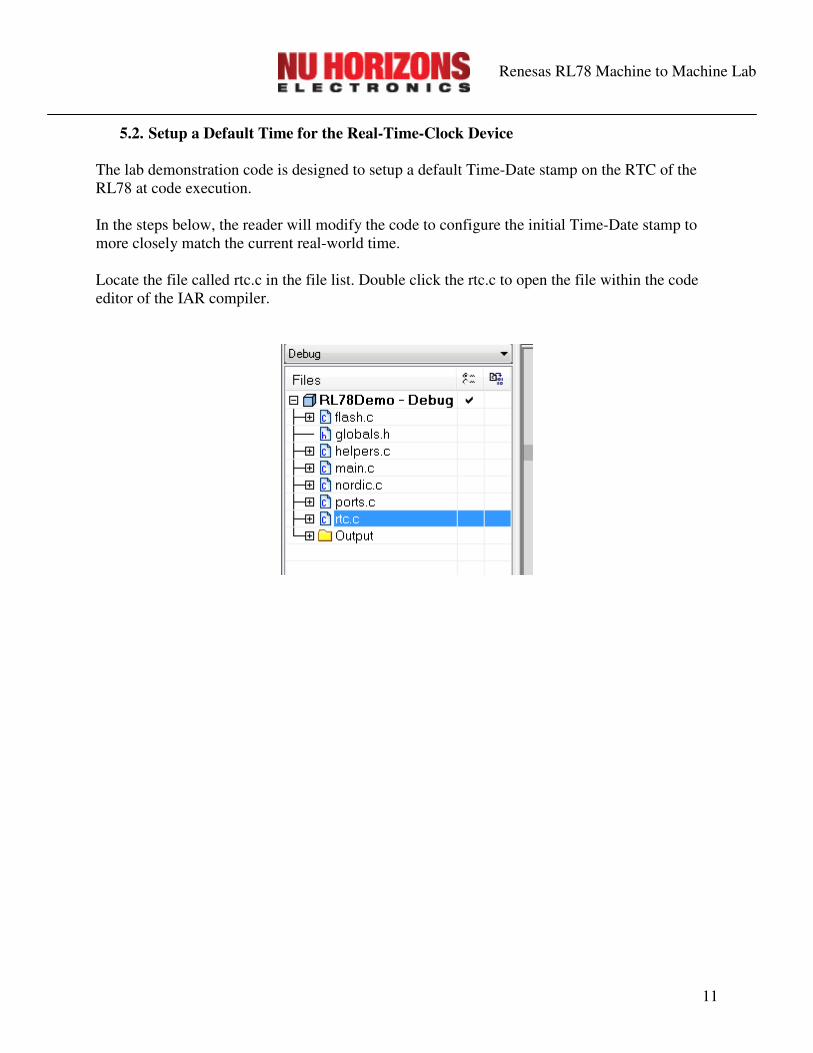
5.2. Setup a Default Time for the Real-Time-Clock Device
The lab demonstration code is designed to setup a default Time-Date stamp on the RTC of the
RL78 at code execution.
In the steps below, the reader will modify the code to configure the initial Time-Date stamp to
more closely match the current real-world time.
Locate the file called rtc.c in the file list. Double click the rtc.c to open the file within the code
editor of the IAR compiler.

12
Renesas RL78 Machine to Machine Lab
The first function within the rtc.c file should be called “SetTime”.
The “SetTime” function is used to both initially configure the RTC to a pre-set time and allow
the user to modify the time during the lab itself.
Locate the lines contained under the “mode==1” as shown in the highlighted area.
Change the Month, Day, Year, Hour, Minute, Second to represent the current time/date.
Note that the YEAR is an 8-bit value therefore 2012 should be represented as 12.
After making the changes, press the “Disk Icon” in the tool bar or use the “Control S” command
to save the updated rtc.c file.

13
Renesas RL78 Machine to Machine Lab
5.3. Show how to compile code
The IAR Compiler and RL78 Demo Kit both provide an integrated environment that allows code
development, compilation, download, and debugging of CPU Code using a single USB interface.
In the previous section, the reader modified the rtc.c file to represent the current real-world
time/date.
This code must be compiled so that it can be downloaded into the CPU.
In order to compile the code, locate the “Project” option on the main toolbar show below.
Select the “Make” option (or use the F7 shortcut) to compile and build an executable image of
the program for the RL78 CPU.

14
Renesas RL78 Machine to Machine Lab
After executing the “Make” process, the message window within IAR should report the build
status and errors/warnings that were encountered during the build process.
Note that both errors and warnings should appear as ZERO.
If there are errors/warnings, return to the previous section and ensure that the updates to the rtc.c
file were completed properly.
15
Renesas RL78 Machine to Machine Lab
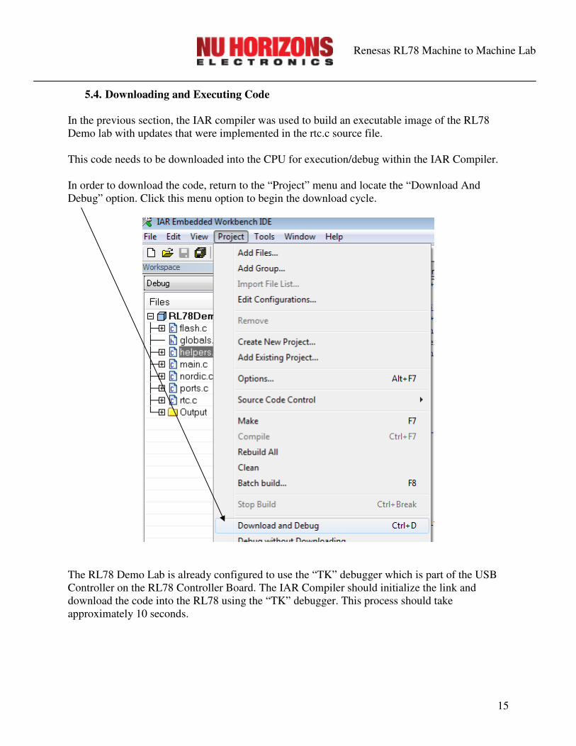
5.4. Downloading and Executing Code
In the previous section, the IAR compiler was used to build an executable image of the RL78
Demo lab with updates that were implemented in the rtc.c source file.
This code needs to be downloaded into the CPU for execution/debug within the IAR Compiler.
In order to download the code, return to the “Project” menu and locate the “Download And
Debug” option. Click this menu option to begin the download cycle.
The RL78 Demo Lab is already configured to use the “TK” debugger which is part of the USB
Controller on the RL78 Controller Board. The IAR Compiler should initialize the link and
download the code into the RL78 using the “TK” debugger. This process should take
approximately 10 seconds.
16
Renesas RL78 Machine to Machine Lab
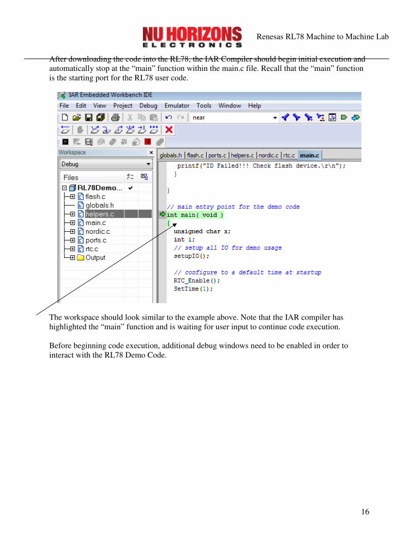
After downloading the code into the RL78, the IAR Compiler should begin initial execution and
automatically stop at the “main” function within the main.c file. Recall that the “main” function
is the starting port for the RL78 user code.
The workspace should look similar to the example above. Note that the IAR compiler has
highlighted the “main” function and is waiting for user input to continue code execution.
Before beginning code execution, additional debug windows need to be enabled in order to
interact with the RL78 Demo Code.

17
Renesas RL78 Machine to Machine Lab
Locate the “View” option on the main toolbar within the IAR Compiler. This menu provides a
variety of windows that can be opened to allow the user to view internal registers, assembly
source, raw memory, and other debug functions provided by the RL78 CPU core and the IAR
Compiler.
Locate the “Terminal I/O” option and click it. This will open a simple text terminal window to
allow the user to connect to the debug UART within the RL78. In debug mode, the UART is
mapped into the Terminal Window.

18
Renesas RL78 Machine to Machine Lab
After selecting the “Terminal I/O” option for the View Menu, the IAR Compiler windows should
appear similar to the example below.
Note that the three main windows � Workspace, Source Code (main.c), and the Terminal are
visible.
Once the main windows are visible, locate the “Debug” menu from the main toolbar within the
IAR Compiler. Select the “GO” option (or F5 shortcut) to begin code execution.
19
Renesas RL78 Machine to Machine Lab
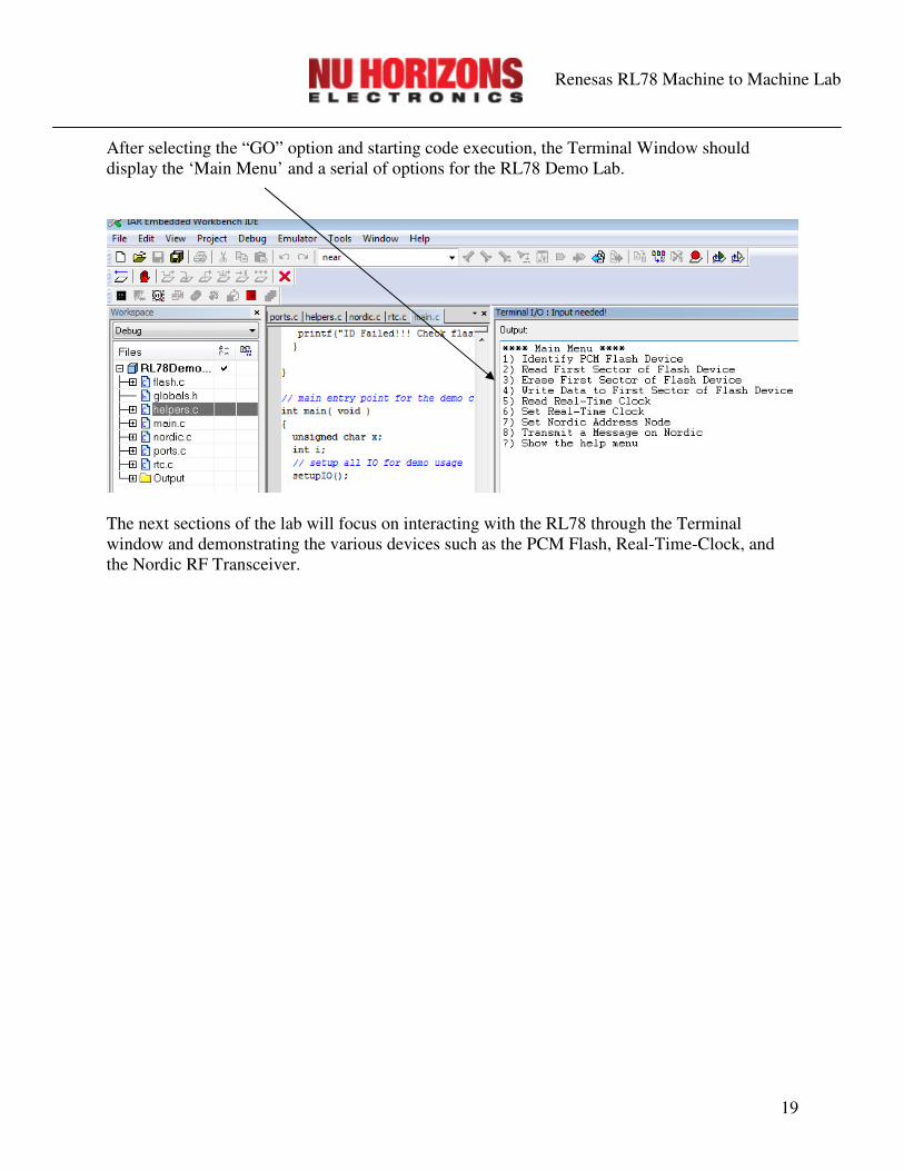
After selecting the “GO” option and starting code execution, the Terminal Window should
display the ‘Main Menu’ and a serial of options for the RL78 Demo Lab.
The next sections of the lab will focus on interacting with the RL78 through the Terminal
window and demonstrating the various devices such as the PCM Flash, Real-Time-Clock, and
the Nordic RF Transceiver.

20
Renesas RL78 Machine to Machine Lab
6. Demonstration and Test
The following sections of this lab will explore the command line menu and demonstrate the
Flash, Real-Time-Clock, and Nordic RF Transceiver.
6.1. Introduce the command line terminal
At the end of section 5, the code compilation, download, and execution should be successful and
the command line terminal should be displayed within the “Terminal I/O” window similar to as
shown below.
21
Renesas RL78 Machine to Machine Lab
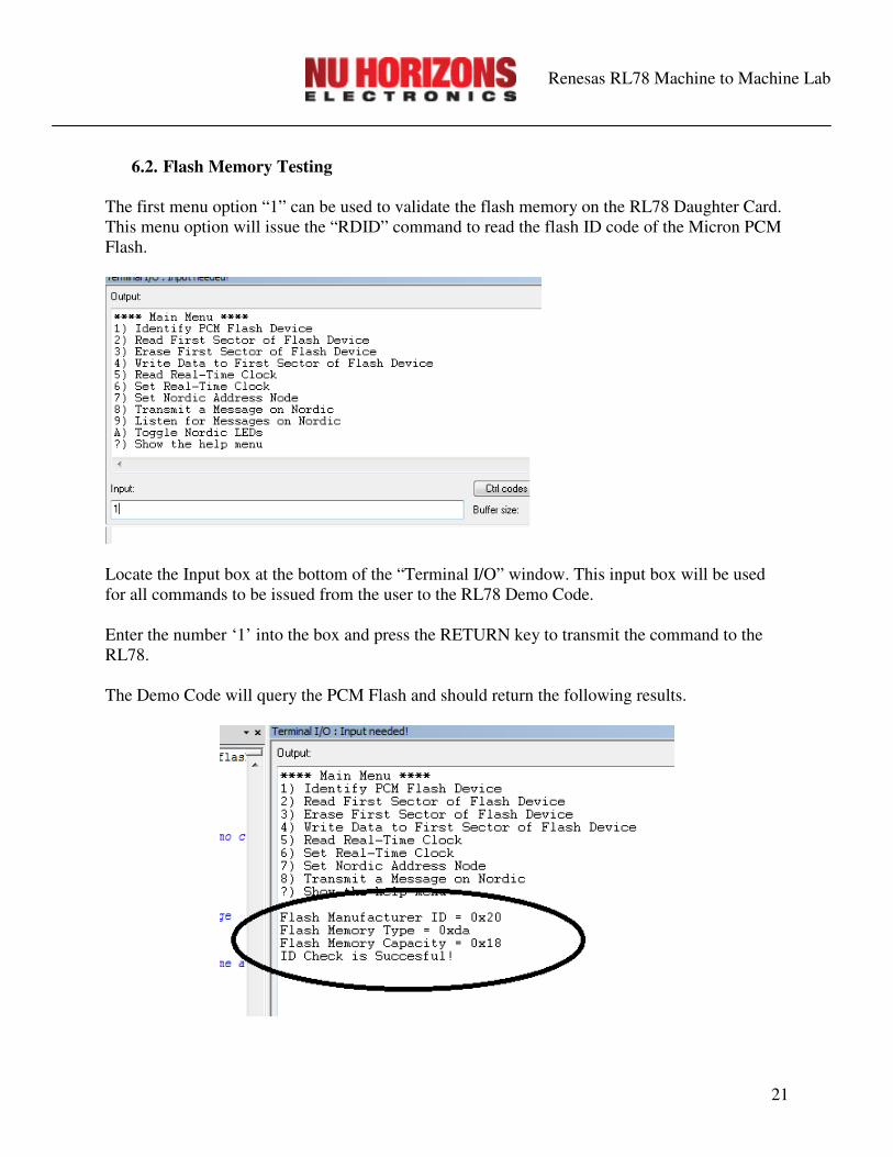
6.2. Flash Memory Testing
The first menu option “1” can be used to validate the flash memory on the RL78 Daughter Card.
This menu option will issue the “RDID” command to read the flash ID code of the Micron PCM
Flash.
Locate the Input box at the bottom of the “Terminal I/O” window. This input box will be used
for all commands to be issued from the user to the RL78 Demo Code.
Enter the number ‘1’ into the box and press the RETURN key to transmit the command to the
RL78.
The Demo Code will query the PCM Flash and should return the following results.

22
Renesas RL78 Machine to Machine Lab
The ID Codes are 0x20, 0xDa, and 0x18 and the “ID Check” is successful. The ID Codes should
match page 19 of the Micron PCM specification for the flash memory. This indicates that the
CPU is properly communicating with the PCM Memory.
Next, enter option ‘2’ in the input box and press the return key. This will read a series of bytes
from flash that have been allocated as a temp area for the RL78 lab.
The flash may return a series of “FF” values as shown above. This would indicate that the flash
is completely blank. However, a previous lab may have been executed on this board and there
may still be contents within the flash.
If your flash is not blank, enter option ‘3’ to erase the flash. The erase cycle should take less than
10ms and appear as shown below.
If option ‘3’ was used to erase the flash, enter option ‘2’ again to validate that the flash is now
blank and matches the readout example at the top of this page.
Once the flash is blank, enter option ‘4’ to write a predefined ASCII series into the flash
memory. Option 4 should report as follows.
After issuing option ‘4’ to generate a write pattern, enter option ‘2’ again to read the flash data.
The flash readout should look similar to the example above, showing an ascending ASCII
sequence.
23
Renesas RL78 Machine to Machine Lab
6.3. Real-Time Clock Testing
In this section, the Real-Time Clock Calendar of the CPU will be tested.
Recall that the rtc.c file was modified to provide a manually set time/date stamp at the start of the
code.
Enter menu option ‘5’ to read the current real time clock’s time/date stamp.
The results should return in the Terminal Window in the format
MONTH / DAY / YEAR HOUR:MINUTE:SECOND
Note that the time should have advanced beyond the manually entered time/date that was
updated in the rtc.c file in section 5 of this lab.
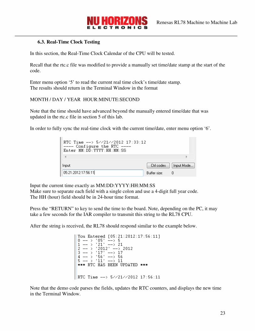
In order to fully sync the real-time clock with the current time/date, enter menu option ‘6’.
Input the current time exactly as MM:DD:YYYY:HH:MM:SS
Make sure to separate each field with a single colon and use a 4-digit full year code.
The HH (hour) field should be in 24-hour time format.
Press the “RETURN” to key to send the time to the board. Note, depending on the PC, it may
take a few seconds for the IAR compiler to transmit this string to the RL78 CPU.
After the string is received, the RL78 should respond similar to the example below.
Note that the demo code parses the fields, updates the RTC counters, and displays the new time
in the Terminal Window.

24
Renesas RL78 Machine to Machine Lab
6.4. Nordic RF Transceiver Testing
The RL78 Demo Lab provides a secondary interface to the Nordic nRF24LE 2.4GHz
transceiver. This device contains an 8051 CPU core, flash memory, clock generators, and a
dedicated RF Transceiver on single device.
The nRF24LE should be pre-loaded with firmware by your lab instructor. The firmware on
the nRF24LE is specifically designed to interact with the RL78 CPU for the purpose of
transmitting and receiving simple messages.
The nRF24 and the RL78 communicate using a SPI bus interface. The RL78 is a master and
the nRF24 is configured as a slave.
The message protocol transmitted by the RL78 consists of the following format.
MM:DD:YY:HH:MN:SS-CCCC-usermessage
Where
MM:DD:YY � Month/Day/Year (coded as a 2-digital year)
HH:MN:SS � Hour/Minute/Second based on the Real-Time-Clock of the RL79
CCCC � a 4-digital ID code assigned by the user
[usermessage] � An 8 character unique message

25
Renesas RL78 Machine to Machine Lab
6.4.1. Configure Node Address for nRF Transceiver
The first step to configure the nRF demo is to setup a unique node address for the demo board.
This can be performed using menu option 7.
Enter menu option ‘7’ and press the return key.
The RL78 will then prompt for a 4-character unique ID Code.
The code can be any 4 alpha/numeric keys.
Enter the code in the input box and press the return key.
Confirmation of the 4-digital code will then be returned on by the RL78 in the Terminal
Window.

26
Renesas RL78 Machine to Machine Lab
6.4.2. Demonstrate “Send Message” on Nordic
After configuring the Node Address, a demonstration of sending a message can be performed. In
order for this test to be useful, a second system should be prepared and waiting in the “Receive
Message” state as detailed in the next section.
In order to transmit a message, select menu option ‘8’ and press the return key.
The RL78 should then prompt for an 8 character user message to be entered.
Type the message into the input box and press the return key.
The RL78 firmware will assembly a payload containing the time stamp data, node id, and the
user message as shown. The message will then be transmitted on the SPI bus between the RL78
and the nRF24. After the message is sent to the nRF24, the RL78 will trigger the actual RF
transmission of the message.
The raw message to be transmitted will be displayed in the terminal window and it should be
received by a second system in the “Receive Message” state as detailed in the next section.
27
Renesas RL78 Machine to Machine Lab
6.4.3. Demonstrate “Receive Message” On Nordic
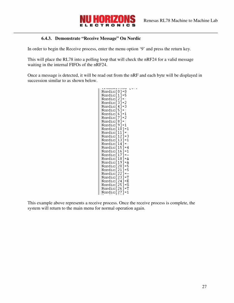
In order to begin the Receive process, enter the menu option ‘9’ and press the return key.
This will place the RL78 into a polling loop that will check the nRF24 for a valid message
waiting in the internal FIFOs of the nRF24.
Once a message is detected, it will be read out from the nRF and each byte will be displayed in
succession similar to as shown below.
This example above represents a receive process. Once the receive process is complete, the
system will return to the main menu for normal operation again.
28
Renesas RL78 Machine to Machine Lab
7. Appendix A – nRF CPU Code Overview
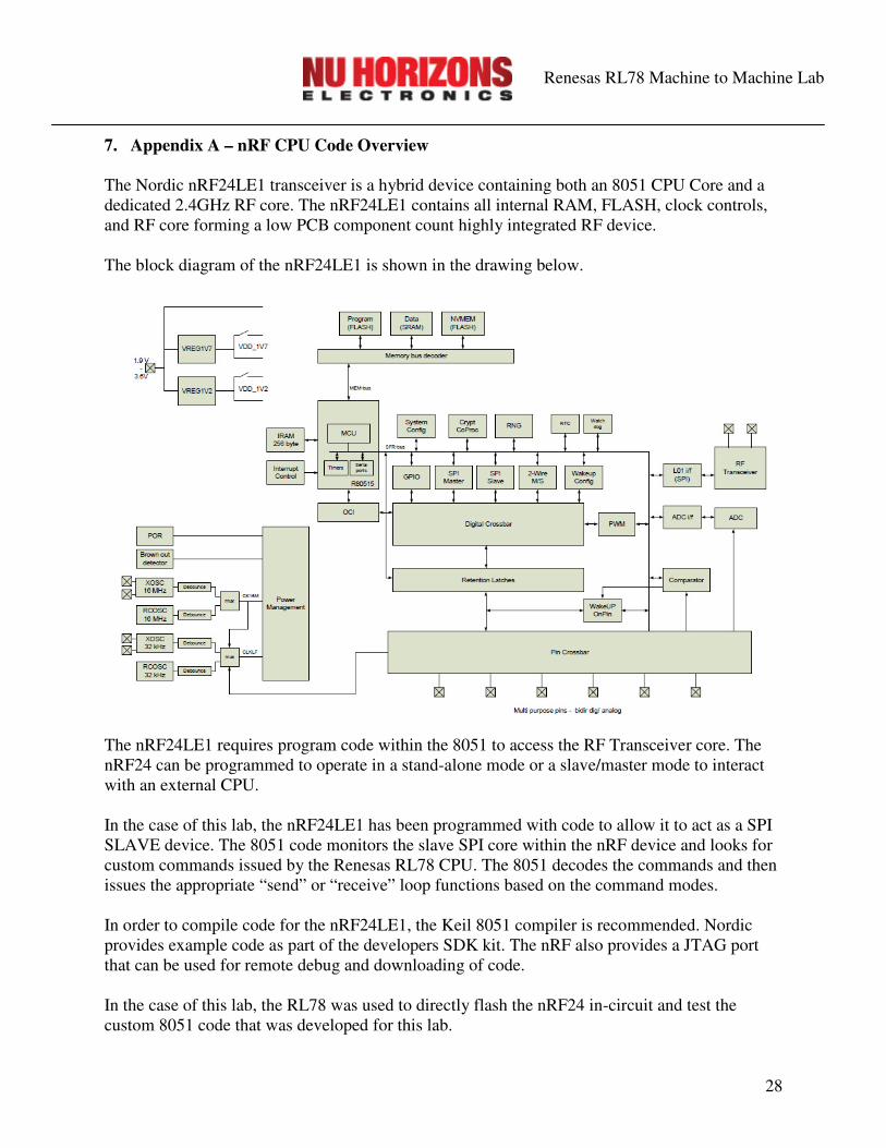
The Nordic nRF24LE1 transceiver is a hybrid device containing both an 8051 CPU Core and a
dedicated 2.4GHz RF core. The nRF24LE1 contains all internal RAM, FLASH, clock controls,
and RF core forming a low PCB component count highly integrated RF device.
The block diagram of the nRF24LE1 is shown in the drawing below.
The nRF24LE1 requires program code within the 8051 to access the RF Transceiver core. The
nRF24 can be programmed to operate in a stand-alone mode or a slave/master mode to interact
with an external CPU.
In the case of this lab, the nRF24LE1 has been programmed with code to allow it to act as a SPI
SLAVE device. The 8051 code monitors the slave SPI core within the nRF device and looks for
custom commands issued by the Renesas RL78 CPU. The 8051 decodes the commands and then
issues the appropriate “send” or “receive” loop functions based on the command modes.
In order to compile code for the nRF24LE1, the Keil 8051 compiler is recommended. Nordic
provides example code as part of the developers SDK kit. The nRF also provides a JTAG port
that can be used for remote debug and downloading of code.
In the case of this lab, the RL78 was used to directly flash the nRF24 in-circuit and test the
custom 8051 code that was developed for this lab.

29
Renesas RL78 Machine to Machine Lab
The basic flow-chart for the 8051 code that was developed for the nRF24 as part of this lab is
shown in the outline below.
Setup IO Ports
Enable RF and Interrupts
Configure Tx/Rx Options
Enable SPI Slave Mode
Get 2nd
SPI ByteSPI Data?Decode
Command
Poll For RecieveTransmit Data
On RF Link
Transmit Data to RL78
The 8051 code for the nRF device is used to configure the nRF24 for operational mode and
enable the SPI Slave. Once in the SPI Slave mode, the code waits for 2 bytes of SPI data to
define the command to be executed. The commands are decoded and then the transmit or receive
operation occurs. In the case of a receive, data is returned to the RL78 using the SPI bus.

30
Renesas RL78 Machine to Machine Lab
7.1. Command Codes
The following table details the command codes accepted by the nRF 8051 firmware.
Command Operation
0x3F 0xyy Sets 3 LED output ports based on the “YY “ value
0x00 0xyy
Through
0x3E 0xyy
Writes bytes “YY” into a transmit buffer. The final write to address 0x3E
both loads the data “YY” into the buffer and issues the RF transmission.
A read operation can also be performed on address 0x3E to return pending
data from a receive operation

31
Renesas RL78 Machine to Machine Lab
8. Appendix B – nRF In-Circuit-Flash Programming
The nRF24LE1 provides a method that can be used to program the on-chip FLASH of the 8051
with new program code. A series of files are provided as part of the RL78Demo lab that can
accomplish this. These files may be used by the reader for future development and provide an
example on how to program the 8051 FLASH of the nRF24LE1.
The nRF24LE1 specification details that the “PROG” pin and the “RESET“ pin are used to enter
the FLASH programming via SPI mode. In order to enter this mode, the PROG pin must be set
to logic(1) and then the RESET pin must be toggled from logic(0)�logic(1). After this
sequence, the SPI pins on the nRF24LE1 are placed into a direct SPI Flash access mode.
The RL78 source files flash.c, hex.c, and nordicfw.c are used to perform the programming
operation.
The file “nordicfw.c” provides a data array which is an intel-hex format PROM file. This file is
the exact firmware image generated from the Keil compiler and this file will be used to program
the contents of the nRF24 flash.
The file “flash.c” provides low-level I/O routines that are used to access the SPI flash port on the
nRF24.
The file “hex.c” provides the high-level flash routine. There is a function called NordicFlash
within the hex.c file and this issues the entire flash programming cycle. The intel-hex image is
read directly from the array defined in the “nordicfw.c” file and is written into the 8051 Flash
memory of the nRF24LE1.
8.1. Generating the nordicfw.c file
A tool has been provided to convert the Keil compiler’s intel-hex file into the nordicfw.c format
allowing the intel-hex nRF24 code to be directly compiled into the RL78 firmware to allow the
in-circuit-flash.
The tool is a Windows EXE called “nordicfw.exe”. This tool reads in the output of the Keil
compiler (assuming the file is called fw.hex) and generates the nordicfw.c file for use within the
RL78 firmware.

32
Renesas RL78 Machine to Machine Lab
9. Appendix C – RL78 Daughter Card Bill Of Materials