NuDAQ DAQ-2204/2205/2206/2208 PXI-2204/2205/2206/2208 · PXI-2204/2205/2206/2208 64/96-CH, High...
84
NuDAQ ® DAQ-2204/2205/2206/2208 PXI-2204/2205/2206/2208 64/96-CH, High Performance Multi-function Data Acquisition Cards User's Guide Recycled Paper
Transcript of NuDAQ DAQ-2204/2205/2206/2208 PXI-2204/2205/2206/2208 · PXI-2204/2205/2206/2208 64/96-CH, High...

NuDAQ® DAQ-2204/2205/2206/2208 PXI-2204/2205/2206/2208
64/96-CH, High Performance Multi-function Data Acquisition Cards
User's Guide
Recycled Paper
©Copyright 2003 ADLINK Technology Inc. All Rights Reserved.
Manual Rev. 1.22: December 19, 2003
Part No: 50-11213-102
The information in this document is subject to change without prior notice in order to improve reliability, design, and function and does not represent a commitment on the part of the manufacturer.
In no event will the manufacturer be liable for direct, indirect, special, in-cidental, or consequential damages arising out of the use or inability to use the product or documentation, even if advised of the possibility of such damages.
This document contains proprietary information protected by copyright. All rights are reserved. No part of this manual may be reproduced by any mechanical, electronic, or other means in any form without prior written permission of the manufacturer.
Trademarks
NuDAQ®, NuIPC®, NuDAM®, NuPRO® are registered trademarks of ADLINK Technology Inc. Other product names mentioned herein are used for identification purposes only and may be trademarks and/or registered trademarks of their respective companies.
Getting Service from ADLINK Customer Satisfaction is top priority for ADLINK TECHNOLOGY INC. If you need any help or service, please contact us.
ADLINK TECHNOLOGY INC. Web Site http://www.adlinktech.com Sales & Service [email protected] TEL +886-2-82265877 FAX +886-2-82265717 Address 9F, No. 166, Jian Yi Road, Chungho City, Taipei, 235 Taiwan
Please email or FAX your detailed information for prompt, satisfactory, and consistent service.
Detailed Company Information Company/Organization
Contact Person
E-mail Address
Address
Country
TEL FAX
Web Site
Questions Product Model
Environment
OS: Computer Brand: M/B: CPU: Chipset: BIOS: Video Card: NIC: Other:
Detail Description
Suggestions for ADLINK
ii • Table of Contents
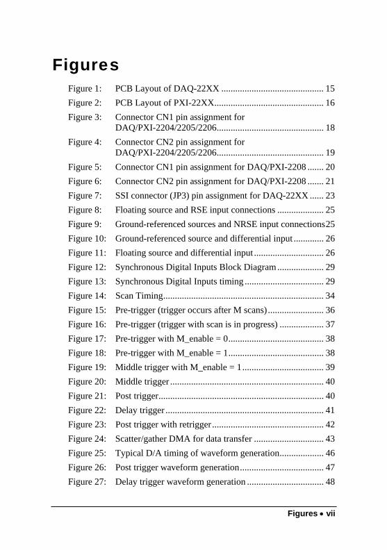
Table of Contents
Tables ...................................................................................... vi
Figures.................................................................................... vii
How to Use This Guide .......................................................... ix
Chapter 1 Introduction........................................................... 1 1.1 Features......................................................................................... 1 1.2 Applications .................................................................................. 3 1.3 Specifications................................................................................ 3 1.4 Software Support ........................................................................ 12
1.4.1 Programming Library ........................................................... 12 1.4.2 D2K-LVIEW: LabVIEW® Driver ........................................ 12 1.4.3 D2K-OCX: ActiveX Controls .............................................. 13
Chapter 2 Installation........................................................... 14 2.1 What You Have .......................................................................... 14 2.2 Unpacking................................................................................... 15 2.3 DAQ/PXI-22XX Layout............................................................. 15 2.4 PCI Configuration....................................................................... 16
Chapter 3 Signal Connections.............................................. 17 3.1 Connectors Pin Assignment ........................................................ 17 3.2 Analog Input Signal Connection................................................. 24
3.2.1 Types of signal sources ........................................................ 24 3.2.2 Input Configurations............................................................. 24
3.2.2.1 Single-ended Connections.........................................................24 3.2.2.2 Differential input mode.............................................................26
Chapter 4 Operation Theory ............................................... 28 4.1 A/D Conversion .......................................................................... 28
4.1.1 DAQ/PXI-2204/2208 AI Data Format ................................. 29 4.1.1.1 Synchronous Digital Inputs (for DAQ/PXI-2204 only) .............29
4.1.2 DAQ/PXI-2205/2206 AI Data Format ................................. 31 4.1.3 Software conversion with polling data transfer acquisition
Table of Contents • iii
mode (Software Polling) ...................................................... 32 4.1.3.1 Specifying Channels, Gains, and input configurations in the
Channel Gain Queue ................................................................32 4.1.4 Programmable scan acquisition mode .................................. 33
4.1.4.1 Scan Timing and Procedure......................................................33 4.1.4.2 Specifying Channels, Gains, and input configurations in the
Channel Gain Queue ................................................................35 4.1.4.3 Trigger Modes ..........................................................................36 4.1.4.4 Bus-mastering DMA Data Transfer ..........................................42
4.2 D/A Conversion .......................................................................... 44 4.2.1 Software Update ................................................................... 45 4.2.2 Timed Waveform Generation............................................... 45
4.2.2.1 Trigger Modes ..........................................................................47 4.2.2.2 Iterative Waveform Generation ................................................49 4.2.2.3 Stop Modes of Scan Update ......................................................50
4.3 Digital I/O................................................................................... 52 4.4 General Purpose Timer/Counter Operation ................................ 53
4.4.1 Timer/Counter functions basics............................................ 53 4.4.2 General Purpose Timer/Counter modes................................ 53
4.4.2.1 Mode1: Simple Gated-Event Counting .....................................54 4.4.2.2 Mode2: Single Period Measurement.........................................54 4.4.2.3 Mode 3: Single Pulse-width Measurement ...............................55 4.4.2.4 Mode 4: Single Gated Pulse Generation ..................................55 4.4.2.5 Mode5: Single Triggered Pulse Generation .............................56 4.4.2.6 Mode6: Re-triggered Single Pulse Generation.........................56 4.4.2.7 Mode7: Single Triggered Continuous Pulse Generation ..........57 4.4.2.8 Mode8: Continuous Gated Pulse Generation ...........................57
4.5 Trigger Sources........................................................................... 58 4.5.1 Software-Trigger .................................................................. 58 4.5.2 External Analog Trigger....................................................... 58
4.5.2.1 Below-Low analog trigger condition ........................................59 4.5.2.2 Above-High analog trigger condition .......................................60 4.5.2.3 Inside-Region analog trigger condition ....................................60 4.5.2.4 High-Hysteresis analog trigger condition ................................61 4.5.2.5 Low-Hysteresis analog trigger condition..................................61
4.5.3 External Digital Trigger ....................................................... 62 4.6 User-controllable Timing Signals ............................................... 63
4.6.1 DAQ timing signals.............................................................. 64 4.6.2 Auxiliary Function Inputs (AFI)........................................... 65 4.6.3 System Synchronization Interface ........................................ 67

iv • Table of Contents
Chapter 5 Calibration........................................................... 70 5.1 Loading Calibration Constants.................................................... 70 5.2 Auto-calibration .......................................................................... 71 5.3 Saving Calibration Constants...................................................... 71
Warranty Policy .................................................................... 72


vi • Tables
Tables Table 1: Programmable input range................................................. 4 Table 2: bandwidth .......................................................................... 5 Table 3: System Noise ..................................................................... 6 Table 4: Input impedance ................................................................ 6 Table 5: CMRR (DC to 60Hz)......................................................... 6 Table 6: Settling time to full-scale step ........................................... 7 Table 7: Legend of 68-pin VHDCI-type connectors...................... 22 Table 8: Legend of SSI connector ................................................. 23 Table 9: Bipolar analog input range and the output digital code on
DAQ/PXI-2204/2208....................................................... 30 Table 10: Unipolar analog input range and the output digital code
on DAQ/PXI-2204/2208.................................................. 30 Table 11: Bipolar analog input range and the output digital code on
DAQ/PXI-2205/2206....................................................... 31 Table 12: Unipolar analog input range and the output digital code
on DAQ/PXI-2205/2206.................................................. 31 Table 13: Bipolar output code table................................................. 44 Table 14: Unipolar output code table............................................... 45 Table 15: Analog trigger SRC1 (EXTATRIG) ideal transfer
characteristic.................................................................... 59 Table 16: Auxiliary function input signals and the corresponding
functionalities .................................................................. 65 Table 17: Summary of SSI timing signals and the corresponding
functionalities as the master or slave ............................... 67
Figures • vii
Figures
Figure 1: PCB Layout of DAQ-22XX ............................................ 15 Figure 2: PCB Layout of PXI-22XX............................................... 16 Figure 3: Connector CN1 pin assignment for
DAQ/PXI-2204/2205/2206.............................................. 18 Figure 4: Connector CN2 pin assignment for
DAQ/PXI-2204/2205/2206.............................................. 19 Figure 5: Connector CN1 pin assignment for DAQ/PXI-2208 ....... 20 Figure 6: Connector CN2 pin assignment for DAQ/PXI-2208 ....... 21 Figure 7: SSI connector (JP3) pin assignment for DAQ-22XX ...... 23 Figure 8: Floating source and RSE input connections .................... 25 Figure 9: Ground-referenced sources and NRSE input connections25 Figure 10: Ground-referenced source and differential input ............. 26 Figure 11: Floating source and differential input .............................. 26 Figure 12: Synchronous Digital Inputs Block Diagram.................... 29 Figure 13: Synchronous Digital Inputs timing .................................. 29 Figure 14: Scan Timing..................................................................... 34 Figure 15: Pre-trigger (trigger occurs after M scans) ........................ 36 Figure 16: Pre-trigger (trigger with scan is in progress) ................... 37 Figure 17: Pre-trigger with M_enable = 0......................................... 38 Figure 18: Pre-trigger with M_enable = 1......................................... 38 Figure 19: Middle trigger with M_enable = 1................................... 39 Figure 20: Middle trigger .................................................................. 40 Figure 21: Post trigger....................................................................... 40 Figure 22: Delay trigger .................................................................... 41 Figure 23: Post trigger with retrigger ................................................ 42 Figure 24: Scatter/gather DMA for data transfer .............................. 43 Figure 25: Typical D/A timing of waveform generation................... 46 Figure 26: Post trigger waveform generation.................................... 47 Figure 27: Delay trigger waveform generation ................................. 48
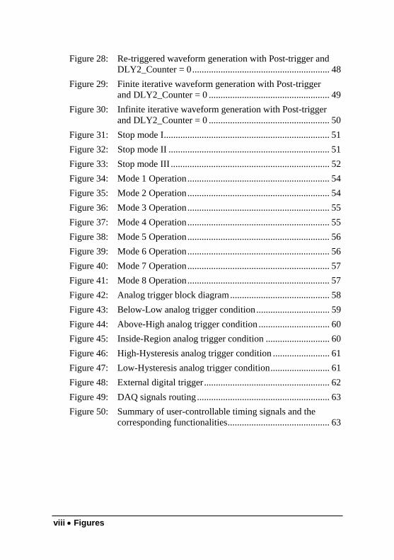
viii • Figures
Figure 28: Re-triggered waveform generation with Post-trigger and DLY2_Counter = 0.......................................................... 48
Figure 29: Finite iterative waveform generation with Post-trigger and DLY2_Counter = 0 ................................................... 49
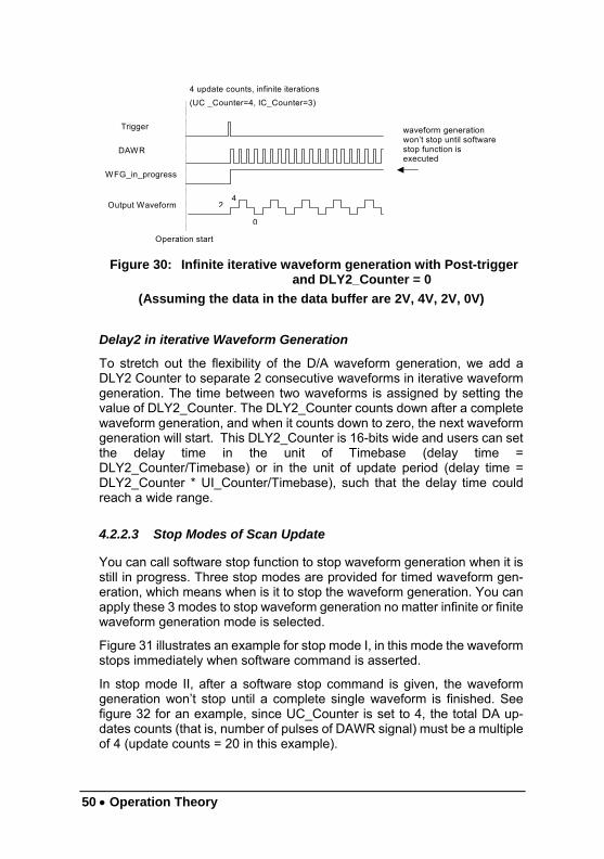
Figure 30: Infinite iterative waveform generation with Post-trigger and DLY2_Counter = 0 ................................................... 50
Figure 31: Stop mode I...................................................................... 51 Figure 32: Stop mode II .................................................................... 51 Figure 33: Stop mode III ................................................................... 52 Figure 34: Mode 1 Operation............................................................ 54 Figure 35: Mode 2 Operation............................................................ 54 Figure 36: Mode 3 Operation............................................................ 55 Figure 37: Mode 4 Operation............................................................ 55 Figure 38: Mode 5 Operation............................................................ 56 Figure 39: Mode 6 Operation............................................................ 56 Figure 40: Mode 7 Operation............................................................ 57 Figure 41: Mode 8 Operation............................................................ 57 Figure 42: Analog trigger block diagram.......................................... 58 Figure 43: Below-Low analog trigger condition............................... 59 Figure 44: Above-High analog trigger condition .............................. 60 Figure 45: Inside-Region analog trigger condition ........................... 60 Figure 46: High-Hysteresis analog trigger condition ........................ 61 Figure 47: Low-Hysteresis analog trigger condition......................... 61 Figure 48: External digital trigger..................................................... 62 Figure 49: DAQ signals routing........................................................ 63 Figure 50: Summary of user-controllable timing signals and the
corresponding functionalities........................................... 63
How to Use This Guide • ix
How to Use This Guide
This manual is designed to help you use/understand the DAQ/PXI-22XX. The manual describes the versatile functions and the operation theory of the DAQ/PXI-22XX. It is divided into five chapters:
Chapter 1 “Introduction” gives an overview of the product features, applications, and specifications.
Chapter 2 “Installation” describes how to install DAQ/PXI-22XX. The layout and the positions of all the connectors on DAQ/PXI-22XX are shown.
Chapter 3 “Signal Connections” describes the connector’s pin as-signment and how to connect the outside signals to DAQ/PXI-22XX.
Chapter 4 “Operation Theory” describes how DAQ/PXI-22XX oper-ates. The A/D, D/A, GPIO, timer/counter, trigger and timing signal routing are introduced.
Chapter 5 “Calibration” describes how to calibrate the DAQ/PXI-22XX for accurate measurements.

Introduction • 1
1
Introduction
The DAQ/PXI-22XX is an advanced data acquisition card based on the 32-bit PCI architecture. High performance designs and the state-of-the-art technology make this card ideal for data logging and signal analysis ap-plications in medical, process control, etc.
1.1 Features
DAQ/PXI-22XX Advanced Data Acquisition Card provides the following advanced features:
• 32-bit PCI-Bus, plug and play
• Up to 96 single-ended inputs or 48 differential inputs, mixing of SE and DI analog input signals are possible
• Up to 1024 words analog input Channel Gain Queue configuration size
• DAQ/PXI-2204/2208: 12-bit Analog input resolution with sampling rate up to 3MHz
• DAQ/PXI-2205: 16-bit Analog input resolution with sampling rate up to 500KHz
• DAQ/PXI-2206: 16-bit Analog input resolution with sampling rate up to 250KHz
• Programmable Bipolar/Unipolar analog input
2 • Introduction
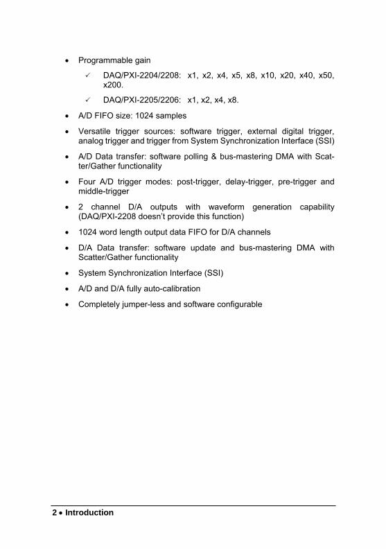
• Programmable gain
DAQ/PXI-2204/2208: x1, x2, x4, x5, x8, x10, x20, x40, x50, x200.
DAQ/PXI-2205/2206: x1, x2, x4, x8.
• A/D FIFO size: 1024 samples
• Versatile trigger sources: software trigger, external digital trigger, analog trigger and trigger from System Synchronization Interface (SSI)
• A/D Data transfer: software polling & bus-mastering DMA with Scat-ter/Gather functionality
• Four A/D trigger modes: post-trigger, delay-trigger, pre-trigger and middle-trigger
• 2 channel D/A outputs with waveform generation capability (DAQ/PXI-2208 doesn’t provide this function)
• 1024 word length output data FIFO for D/A channels
• D/A Data transfer: software update and bus-mastering DMA with Scatter/Gather functionality
• System Synchronization Interface (SSI)
• A/D and D/A fully auto-calibration
• Completely jumper-less and software configurable
Introduction • 3
1.2 Applications
• Automotive Testing
• Cable Testing
• Transient signal measurement
• ATE
• Laboratory Automation
• Biotech measurement
1.3 Specifications
♦ Analog Input (AI)
• Number of channels: (programmable)
DAQ-2204/2205/2206: 64 single-ended (SE) or 32 differential input (DI)
DAQ-2208: 96 single-ended (SE) or 48 differential input (DI)
Mixing of SE and DI analog signal sources (Software selectable per channel)
• A/D converter
2204/2208: LT1412 or equivalent
2205: AD7665 or equivalent
2206: AD7663 or equivalent
• Maximum sampling rate:
2204/2208: 3MS/s (for single channel)
2205: 500KS/s
2206: 250KS/s
• Resolution:
2204/2208: 12 bits, No missing codes
2205/2206: 16 bits, No missing codes
• Input coupling: DC
4 • Introduction
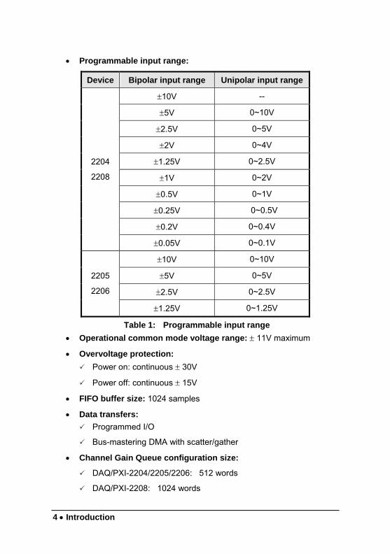
• Programmable input range:
Device Bipolar input range Unipolar input range
±10V --
±5V 0~10V
±2.5V 0~5V
±2V 0~4V
±1.25V 0~2.5V
±1V 0~2V
±0.5V 0~1V
±0.25V 0~0.5V
±0.2V 0~0.4V
2204
2208
±0.05V 0~0.1V
±10V 0~10V
±5V 0~5V
±2.5V 0~2.5V
2205
2206
±1.25V 0~1.25V
Table 1: Programmable input range • Operational common mode voltage range: ± 11V maximum
• Overvoltage protection: Power on: continuous ± 30V
Power off: continuous ± 15V
• FIFO buffer size: 1024 samples
• Data transfers: Programmed I/O
Bus-mastering DMA with scatter/gather
• Channel Gain Queue configuration size:
DAQ/PXI-2204/2205/2206: 512 words
DAQ/PXI-2208: 1024 words
Introduction • 5
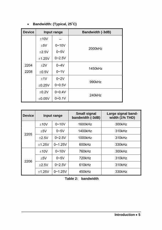
• Bandwidth: (Typical, 25˚C)
Device Input range Bandwidth (-3dB)
±10V
±5V
±2.5V
±1.25V
--
0~10V
0~5V
0~2.5V
2000kHz
±2V
±0.5V
0~4V
0~1V 1450kHz
±1V
±0.25V
0~2V
0~0.5V 990kHz
2204
2208
±0.2V
±0.05V
0~0.4V
0~0.1V 240kHz
Device Input range Small signal bandwidth (-3dB)
Large signal band-width (1% THD)
±10V 0~10V 1600kHz 300kHz
±5V 0~5V 1400kHz 310kHz
±2.5V 0~2.5V 1000kHz 310kHz 2205
±1.25V 0~1.25V 600kHz 330kHz
±10V 0~10V 760kHz 300kHz
±5V 0~5V 720kHz 310kHz
±2.5V 0~2.5V 610kHz 310kHz 2206
±1.25V 0~1.25V 450kHz 330kHz
Table 2: bandwidth

6 • Introduction
• System Noise (LSBrms, including Quantization, Typical, 25˚C)
Device Input Range System Noise Input Range System Noise
±10V 0.95 LSBrms 0~10V 1.5 LSBrms
±5V 1.0 LSBrms 0~5V 1.6 LSBrms
±2.5V 1.1 LSBrms 0~2.5V 1.7 LSBrms 2205
±1.25V 1.3 LSBrms 0~1.25V 1.9 LSBrms
±10V 0.8 LSBrms 0~10V 0.9 LSBrms
±5V 0.85 LSBrms 0~5V 1.0 LSBrms
±2.5V 0.85 LSBrms 0~2.5V 1.0 LSBrms 2206
±1.25V 0.9 LSBrms 0~1.25V 1.2 LSBrms
Table 3: System Noise
• Input impedance
Normal Power On Power Off Overload
1GΩ / 100pF 820Ω 820Ω
Table 4: Input impedance
• CMRR (DC to 60Hz, Typical)
Device Input Range CMRR Input Range CMRR
2204
2208 All ranges 90dB -- --
±10V 83dB 0~10V 87dB
±5V 87dB 0~5V 90dB
±2.5V 90dB 0~2.5V 92dB
2205
2206
±1.25V 92dB 0~1.25V 93dB
Table 5: CMRR (DC to 60Hz)
Introduction • 7
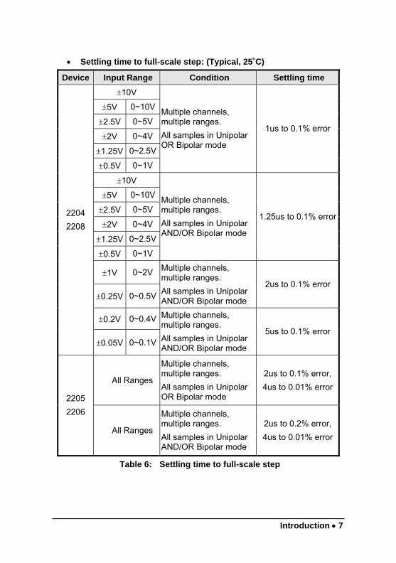
• Settling time to full-scale step: (Typical, 25˚C)
Device Input Range Condition Settling time ±10V
±5V 0~10V
±2.5V 0~5V
±2V 0~4V
±1.25V 0~2.5V
±0.5V 0~1V
Multiple channels, multiple ranges. All samples in Unipolar OR Bipolar mode
1us to 0.1% error
±10V
±5V 0~10V
±2.5V 0~5V
±2V 0~4V
±1.25V 0~2.5V
±0.5V 0~1V
Multiple channels, multiple ranges. All samples in Unipolar AND/OR Bipolar mode
1.25us to 0.1% error
±1V 0~2V
±0.25V 0~0.5V
Multiple channels, multiple ranges. All samples in Unipolar AND/OR Bipolar mode
2us to 0.1% error
±0.2V 0~0.4V
2204 2208
±0.05V 0~0.1V
Multiple channels, multiple ranges. All samples in Unipolar AND/OR Bipolar mode
5us to 0.1% error
All Ranges
Multiple channels, multiple ranges. All samples in Unipolar OR Bipolar mode
2us to 0.1% error, 4us to 0.01% error
2205 2206
All Ranges
Multiple channels, multiple ranges. All samples in Unipolar AND/OR Bipolar mode
2us to 0.2% error, 4us to 0.01% error
Table 6: Settling time to full-scale step
8 • Introduction
• Time-base source: Internal 40MHz or External clock Input (fmax: 40MHz, fmin: 1MHz, 50% duty cycle)
• Trigger modes: post-trigger, delay-trigger, pre-trigger and mid-dle-trigger
• Offset error:
Before calibration: ±60mV max
After calibration: ±1mV max
• Gain error: (relative to calibration reference)
Before calibration: ±0.6% of reading
After calibration: (gain = 1)
±0.03% of reading max for DAQ/PXI-2204/2208
±0.01% of reading max for DAQ/PXI-2205/2206
Gain ≠ 1 with gain error adjusted to 0 at gain = 1:
±0.05% of reading max
♦ Analog Output (AO) (DAQ/PXI-2208 doesn’t provide this function)
• Number of channels: 2 analog voltage outputs
• D/A converter: LTC7545 or equivalent
• Maximum update rate: 1MS/s
• Resolution: 12 bits
• FIFO buffer size:
512 samples per channel when both channels are enabled for timed output.
1024 samples when only one channel is used for timed output.
• Data transfers:
Programmed I/O,
Bus-mastering DMA with scatter/gather
• Output range: ±10V, 0~10V, ±AOEXTREF, 0~AOEXTREF
• Settling time: 3µS to 0.5LSB accuracy
• Slew rate: 20V/uS
• Output coupling: DC
Introduction • 9
• Protection: Short-circuit to ground
• Output impedance: 0.1Ω typical
• Output driving: ±5mA max.
• Stability: Any passive load, up to 1500pF
• Power-on state: 0V steady-state
• Power-on glitch: ±1V/500uS
• Relative accuracy:
±0.5 LSB typical, ±1 LSB max
• DNL:
±0.5 LSB typical, ±1.2 LSB max
• Offset error:
Before calibration: ±80mV max
After calibration: ±1mV max
• Gain error:
Before calibration: ±0.8% of output max
After calibration: ±0.02% of output max
♦ General Purpose Digital I/O (G.P. DIO, 82C55A)
• Number of channels: 24 programmable Input/Output
• Compatibility: TTL
• Input voltage:
Logic Low: VIL=0.8 V max.; IIL=0.2mA max.
High: VIH=2.0V max.; IIH=0.02mA max
• Output voltage:
Low: VOL=0.5 V max.; IOL=8mA max.
High: VOH=2.7V min; IOH=400µA
• Synchronous Digital Inputs (SDI): Supported by DAQ/PXI-2204 only
• Number of channels: 4 digital inputs sampled simultaneously with the analog signal input.
• Compatibility: TTL/CMOS

10 • Introduction
• Input voltage:
Logic Low: VIL=0.8 V max.; IIL=0.2mA max.
High: VIH=2.0V max.; IIH=0.02mA max
♦ General Purpose Timer/Counter (GPTC) (DAQ/PXI-2208 doesn’t provide this function)
• Number of channels: 2 independent Up/Down Timer/Counters
• Resolution: 16 bits
• Compatibility: TTL
• Clock source: Internal or external
• Max source frequency: 10MHz
♦ Analog Trigger (A.Trig)
• Source: All analog input channels; external analog trigger (EXTATRIG)
• Level: ±Full-scale, internal; ±10V external
• Resolution: 8 bits
• Slope: Positive or negative (software selectable)
• Hysteresis: Programmable
• Bandwidth: 400khz
• External Analog Trigger Input (EXTATRIG):
Input impedance: 40KΩ for DAQ/PXI-2204/2208
20KΩ for DAQ/PXI-2205/2206
• Coupling: DC
• Protection: Continuous ± 35V maximum
♦ Digital Trigger (D.Trig)
• Compatibility: TTL/CMOS
• Response: Rising or falling edge
• Pulse Width: 10ns min
♦ System Synchronous Interface (SSI)
• Trigger lines: 7

Introduction • 11
♦ Stability
• Recommended warm-up time: 15 minutes
• On-board calibration reference:
Level: 5.000V
Temperature coefficient: ±2ppm/°C
Long-term stability: 6ppm/1000Hr
♦ Physical
• Dimension:
175mm by 107mm for DAQ-22XX
Standard CompactPCI form factor for PXI-22XX
• I/O connector: 68-pin female VHDCI type (e.g. AMP-787254-1)
♦ Power Requirement (typical)
• +5VDC:
1.3A for DAQ/PXI-2204
1.2A for DAQ/PXI-2205/2206
950mA for DAQ/PXI-2208
♦ Operating Environment
• Ambient temperature: 0 to 55°C
• Relative humidity: 10% to 90% non-condensing
♦ Storage Environment
• Ambient temperature: -20 to 70°C
• Relative humidity: 5% to 95% non-condensing

12 • Introduction
1.4 Software Support
ADLINK provides versatile software drivers and packages for users’ dif-ferent approach to building up a system. ADLINK not only provides pro-gramming libraries such as DLL for most Windows based systems, but also provide drivers for other software packages such as LabVIEW®.
All software options are included in the ADLINK CD. Non-free software drivers are protected with licensing codes. Without the software code, you can install and run the demo version for two hours for trial/demonstration purposes. Please contact ADLINK dealers to purchase the formal license.
1.4.1 Programming Library
For customers who are writing their own programs, we provide function libraries for many different operating systems, including:
• D2K-DASK: Include device drivers and DLL for Windows 98, Windows NT and Windows 2000. DLL is binary compatible across Windows 98, Windows NT and Windows 2000. This means all applications developed with D2K-DASK are compatible across Windows 98, Windows NT and Windows 2000. The developing environment can be VB, VC++, Delphi, BC5, or any Windows programming language that allows calls to a DLL. The user’s guide and function reference manual of D2K-DASK are in the CD. (\\Manual_PDF\Software\D2K-DASK)
• D2K-DASK/X: Include device drivers and shared library for Linux. The developing environment can be Gnu C/C++ or any program-ming language that allows linking to a shared library. The user's guide and function reference manual of D2K-DASK/X are in the CD. (\Manual_PDF\Software\D2K-DASK-X.)
1.4.2 D2K-LVIEW: LabVIEW® Driver
D2K-LVIEW contains the VIs, which are used to interface with NI’s Lab-VIEW® software package. The D2K-LVIEW supports Windows 98/NT/2000. The LabVIEW® drivers is shipped free with the card. You can install and use them without a license. For detailed information about D2K-LVIEW, please refer to the user’s guide in the CD.
(\\Manual_PDF\Software\D2K-LVIEW)
Introduction • 13
1.4.3 D2K-OCX: ActiveX Controls
We suggest customers who are familiar with ActiveX controls and VB/VC++ programming use D2K-OCX ActiveX control component libraries for developing applications. D2K-OCX is designed for Windows 98/NT/2000. For more detailed information about D2K-OCX, please refer to the user's guide in the CD. (\Manual_PDF\Software\D2K-OCX\D2K-OCX.PDF)
The above software drivers are shipped with the card. Please refer to the “Software Installation Guide” in the package to install these drivers.
In addition, ADLINK supplies ActiveX control software DAQBench. DAQBench is a collection of ActiveX controls for measurement or auto-mation applications. With DAQBench, you can easily develop custom user interfaces to display your data, analyze data you acquired or received from other sources, or integrate with popular applications or other data sources. For more detailed information about DAQBench, please refer to the user's guide in the CD.
(\Manual_PDF\Software\DAQBench\DAQBenchManual.PDF)
You can also get a free 4-hour evaluation version of DAQBench from the CD.
DAQBench is not free. Please contact ADLINK dealer or ADLINK to pur-chase the software license.
14 • Installation
2
Installation
This chapter describes how to install the DAQ/PXI-22XX. The contents of the package and unpacking information that you should be aware of are outlined first.
The DAQ/PXI-22XX performs an automatic configuration of the IRQ, and port address. Users can use software utility, PCI_SCAN to read the system configuration.
2.1 What You Have
In addition to this User's Guide, the package includes the following items:
• DAQ/PXI-22XX Multi-function Data Acquisition Card
• ADLINK All-in-one Compact Disc
• Software Installation Guide
If any of these items are missing or damaged, contact the dealer from whom you purchased the product. Save the shipping materials and carton in case you want to ship or store the product in the future.
Installation • 15
2.2 Unpacking
Your DAQ/PXI-22XX SERIES card contains electro-static sensitive com-ponents that can be easily be damaged by static electricity.
Therefore, the card should be handled on a grounded anti-static mat. The operator should be wearing an anti-static wristband, grounded at the same point as the anti-static mat.
Inspect the card module carton for obvious damages. Shipping and han-dling may cause damage to your module. Be sure there are no shipping and handling damages on the modules carton before continuing.
After opening the card module carton, extract the system module and place it only on a grounded anti-static surface with component side up.
Again, inspect the module for damages. Press down on all the socketed IC's to make sure that they are properly seated. Do this only with the module placed on a firm flat surface.
Note: DO NOT APPLY POWER TO THE CARD IF IT HAS BEEN DAMAGED.
You are now ready to install your DAQ/PXI-22XX.
2.3 DAQ/PXI-22XX Layout
Figure 1: PCB Layout of DAQ-22XX
16 • Installation
Figure 2: PCB Layout of PXI-22XX
2.4 PCI Configuration
1. Plug and Play:
As a plug and play component, the card requests an interrupt number via its PCI controller. The system BIOS responds with an interrupt assignment based on the card information and on known system parameters. These system parameters are determined by the installed drivers and the hardware load seen by the system.
2. Configuration:
The board configuration is done on a board-by-board basis for all PCI boards on your system. Because configuration is controlled by the system and software, there is no jumper setting required for base-address, DMA, and interrupt IRQ.
The configuration is subject to change with every boot of the sys-tem as new boards are added or removed.
3. Trouble shooting:
If your system doesn’t boot or if you experience erratic operation with your PCI board in place, it’s likely caused by an interrupt con-flict (perhaps the BIOS Setup is incorrectly configured). In general, the solution, once you determine it is not a simple oversight, is to consult the BIOS documentation that comes with your system.

Signal Connections • 17
3
Signal Connections
This chapter describes the connectors of the DAQ/PXI-22XX, and the signal connection between the DAQ/PXI-22XX and external devices.
3.1 Connectors Pin Assignment
DAQ/PXI-22XX is equipped with two 68-pin VHDCI-type connectors (AMP-787254-1). It is used for digital input / output, analog input / output, and timer/counter signaling, etc. One 20-pin ribbon male connector is used for SSI (System Synchronous Interface) in DAQ-22XX. The pin assignment for the connectors are illustrated in the Figure 3-7.

18 • Signal Connections
AI0 (AIH0) 1 35 (AIL0) AI32 AI1 (AIH1) 2 36 (AIL1) AI33 AI2 (AIH2) 3 37 (AIL2) AI34 AI3 (AIH3) 4 38 (AIL3) AI35 AI4 (AIH4) 5 39 (AIL4) AI36 AI5 (AIH5) 6 40 (AIL5) AI37 AI6 (AIH6) 7 41 (AIL6) AI38 AI7 (AIH7) 8 42 (AIL7) AI39 AI8 (AIH8) 9 43 (AIL8) AI40 AI9 (AIH9) 10 44 (AIL9) AI41
AI10 (AIH10) 11 45 (AIL10) AI42 AI11 (AIH11) 12 46 (AIL11) AI43 AI12 (AIH12) 13 47 (AIL12) AI44 AI13 (AIH13) 14 48 (AIL13) AI45 AI14 (AIH14) 15 49 (AIL14) AI46 AI15 (AIH15) 16 50 (AIL15) AI47
AISENSE 17 51 AIGND AI16 (AIH16) 18 52 (AIL16) AI48 AI17 (AIH17) 19 53 (AIL17) AI49 AI18 (AIH18) 20 54 (AIL18) AI50 AI19 (AIH19) 21 55 (AIL19) AI51 AI20 (AIH20) 22 56 (AIL20) AI52 AI21 (AIH21) 23 57 (AIL21) AI53 AI22 (AIH22) 24 58 (AIL22) AI54 AI23 (AIH23) 25 59 (AIL23) AI55 AI24 (AIH24) 26 60 (AIL24) AI56 AI25 (AIH25) 27 61 (AIL25) AI57 AI26 (AIH26) 28 62 (AIL26) AI58 AI27 (AIH27) 29 63 (AIL27) AI59 AI28 (AIH28) 30 64 (AIL28) AI60 AI29 (AIH29) 31 65 (AIL29) AI61 AI30 (AIH30) 32 66 (AIL30) AI62 AI31 (AIH31) 33 67 (AIL31) AI63
EXTATRIG 34 68 AIGND
Figure 3: Connector CN1 pin assignment for DAQ/PXI-2204/2205/2206
* Symbols in “()” are for differential mode connection.
Signal Connections • 19
DA0OUT 1 35 AOGND DA1OUT 2 36 AOGND
AOEXTREF 3 37 AOGND NC 4 38 NC
DGND 5 39 DGND EXTWFTRIG 6 40 DGND
EXTDTRIG 7 41 DGND SSHOUT 8 42 SDI0 / DGND*
RESERVED 9 43 SDI1 / DGND* RESERVED 10 44 SDI2 / DGND*
AFI1 11 45 SDI3 / DGND* AFI0 12 46 DGND
GPTC0_SRC 13 47 DGND GPTC0_GATE 14 48 DGND
GPTC0_UPDOWN 15 49 DGND GPTC0_OUT 16 50 DGND GPTC1_SRC 17 51 DGND
GPTC1_GATE 18 52 DGND GPTC1_UPDOWN 19 53 DGND
GPTC1_OUT 20 54 DGND EXTTIMEBASE 21 55 DGND
PB7 22 56 PB6 PB5 23 57 PB4 PB3 24 58 PB2 PB1 25 59 PB0 PC7 26 60 PC6 PC5 27 61 PC4
DGND 28 62 DGND PC3 29 63 PC2 PC1 30 64 PC0 PA7 31 65 PA6 PA5 32 66 PA4 PA3 33 67 PA2 PA1 34 68 PA0
Figure 4: Connector CN2 pin assignment for DAQ/PXI-2204/2205/2206
*Pin 42~45 are SDI<0..3> for DAQ/PXI-2204 ; DGND for DAQ/PXI-2205/2206

20 • Signal Connections
AI0 (AIH0) 1 35 (AIL0) AI48 AI1 (AIH1) 2 36 (AIL1) AI49 AI2 (AIH2) 3 37 (AIL2) AI50 AI3 (AIH3) 4 38 (AIL3) AI51 AI4 (AIH4) 5 39 (AIL4) AI52 AI5 (AIH5) 6 40 (AIL5) AI53 AI6 (AIH6) 7 41 (AIL6) AI54 AI7 (AIH7) 8 42 (AIL7) AI55
AISENSE 9 43 AIGND AI8 (AIH8) 10 44 (AIL8) AI56 AI9 (AIH9) 11 45 (AIL9) AI57
AI10 (AIH10) 12 46 (AIL10) AI58 AI11 (AIH11) 13 47 (AIL11) AI59 AI12 (AIH12) 14 48 (AIL12) AI60 AI13 (AIH13) 15 49 (AIL13) AI61 AI14 (AIH14) 16 50 (AIL14) AI62 AI15 (AIH15) 17 51 (AIL15) AI63 AI16 (AIH16) 18 52 (AIL16) AI64 AI17 (AIH17) 19 53 (AIL17) AI65 AI18 (AIH18) 20 54 (AIL18) AI66 AI19 (AIH19) 21 55 (AIL19) AI67 AI20 (AIH20) 22 56 (AIL20) AI68 AI21 (AIH21) 23 57 (AIL21) AI69 AI22 (AIH22) 24 58 (AIL22) AI70 AI23 (AIH23) 25 59 (AIL23) AI71
AIGND 26 60 AIGND AI24 (AIH24) 27 61 (AIL24) AI72 AI25 (AIH25) 28 62 (AIL25) AI73 AI26 (AIH26) 29 63 (AIL26) AI74 AI27 (AIH27) 30 64 (AIL27) AI75 AI28 (AIH28) 31 65 (AIL28) AI76 AI29 (AIH29) 32 66 (AIL29) AI77 AI30 (AIH30) 33 67 (AIL30) AI78 AI31 (AIH31) 34 68 (AIL31) AI79
Figure 5: Connector CN1 pin assignment for DAQ/PXI-2208
* Symbols in “()” are for differential mode connection.
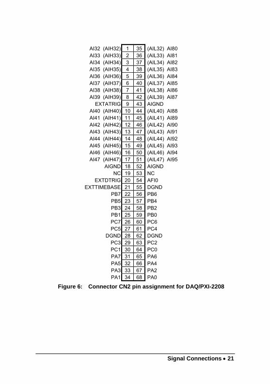
Signal Connections • 21
AI32 (AIH32) 1 35 (AIL32) AI80 AI33 (AIH33) 2 36 (AIL33) AI81 AI34 (AIH34) 3 37 (AIL34) AI82 AI35 (AIH35) 4 38 (AIL35) AI83 AI36 (AIH36) 5 39 (AIL36) AI84 AI37 (AIH37) 6 40 (AIL37) AI85 AI38 (AIH38) 7 41 (AIL38) AI86 AI39 (AIH39) 8 42 (AIL39) AI87
EXTATRIG 9 43 AIGND AI40 (AIH40) 10 44 (AIL40) AI88 AI41 (AIH41) 11 45 (AIL41) AI89 AI42 (AIH42) 12 46 (AIL42) AI90 AI43 (AIH43) 13 47 (AIL43) AI91 AI44 (AIH44) 14 48 (AIL44) AI92 AI45 (AIH45) 15 49 (AIL45) AI93 AI46 (AIH46) 16 50 (AIL46) AI94 AI47 (AIH47) 17 51 (AIL47) AI95
AIGND 18 52 AIGND NC 19 53 NC
EXTDTRIG 20 54 AFI0 EXTTIMEBASE 21 55 DGND
PB7 22 56 PB6 PB5 23 57 PB4 PB3 24 58 PB2 PB1 25 59 PB0 PC7 26 60 PC6 PC5 27 61 PC4
DGND 28 62 DGND PC3 29 63 PC2 PC1 30 64 PC0 PA7 31 65 PA6 PA5 32 66 PA4 PA3 33 67 PA2 PA1 34 68 PA0
Figure 6: Connector CN2 pin assignment for DAQ/PXI-2208
22 • Signal Connections
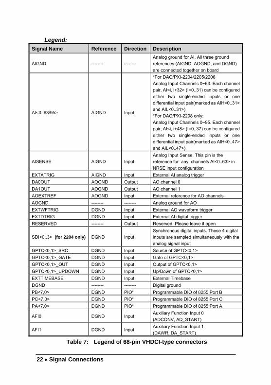
Legend: Signal Name Reference Direction Description
AIGND -------- -------- Analog ground for AI. All three ground references (AIGND, AOGND, and DGND) are connected together on board
AI<0..63/95> AIGND Input
*For DAQ/PXI-2204/2205/2206 Analog Input Channels 0~63. Each channel pair, AI<i, i+32> (I=0..31) can be configured either two single-ended inputs or one differential input pair(marked as AIH<0..31> and AIL<0..31>) *For DAQ/PXI-2208 only: Analog Input Channels 0~95. Each channel pair, AI<i, i+48> (I=0..37) can be configured either two single-ended inputs or one differential input pair(marked as AIH<0..47> and AIL<0..47>)
AISENSE AIGND Input Analog Input Sense. This pin is the reference for any channels AI<0..63> in NRSE input configuration
EXTATRIG AIGND Input External AI analog trigger DA0OUT AOGND Output AO channel 0 DA1OUT AOGND Output AO channel 1 AOEXTREF AOGND Input External reference for AO channels AOGND -------- -------- Analog ground for AO EXTWFTRIG DGND Input External AO waveform trigger EXTDTRIG DGND Input External AI digital trigger RESERVED -------- Output Reserved. Please leave it open
SDI<0..3> (for 2204 only) DGND Input Synchronous digital inputs. These 4 digital inputs are sampled simultaneously with the analog signal input
GPTC<0,1>_SRC DGND Input Source of GPTC<0,1> GPTC<0,1>_GATE DGND Input Gate of GPTC<0,1> GPTC<0,1>_OUT DGND Input Output of GPTC<0,1> GPTC<0,1>_UPDOWN DGND Input Up/Down of GPTC<0,1> EXTTIMEBASE DGND Input External Timebase DGND -------- -------- Digital ground PB<7,0> DGND PIO* Programmable DIO of 8255 Port B PC<7,0> DGND PIO* Programmable DIO of 8255 Port C PA<7,0> DGND PIO* Programmable DIO of 8255 Port A
AFI0 DGND Input Auxiliary Function Input 0 (ADCONV, AD_START)
AFI1 DGND Input Auxiliary Function Input 1 (DAWR, DA_START)
Table 7: Legend of 68-pin VHDCI-type connectors
Signal Connections • 23
SSI_TIMEBASE 1 2 DGND
SSI_ADCONV 3 4 DGND SSI_DAWR / RESERVED* 5 6 DGND
SSI_SCAN_START 7 8 DGND RESERVED 9 10 DGND
SSI_AD_TRIG 11 12 DGND SSI_DA_TRIG / RESERVED* 13 14 DGND
RESERVED 15 16 DGND RESERVED 17 18 DGND RESERVED 19 20 DGND
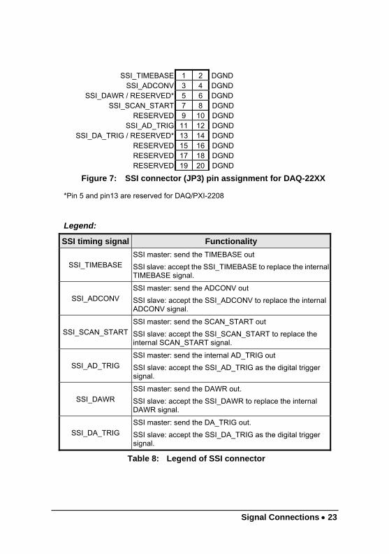
Figure 7: SSI connector (JP3) pin assignment for DAQ-22XX
*Pin 5 and pin13 are reserved for DAQ/PXI-2208
Legend:
SSI timing signal Functionality
SSI_TIMEBASE SSI master: send the TIMEBASE out SSI slave: accept the SSI_TIMEBASE to replace the internal TIMEBASE signal.
SSI_ADCONV SSI master: send the ADCONV out SSI slave: accept the SSI_ADCONV to replace the internal ADCONV signal.
SSI_SCAN_STARTSSI master: send the SCAN_START out SSI slave: accept the SSI_SCAN_START to replace the internal SCAN_START signal.
SSI_AD_TRIG SSI master: send the internal AD_TRIG out SSI slave: accept the SSI_AD_TRIG as the digital trigger signal.
SSI_DAWR SSI master: send the DAWR out. SSI slave: accept the SSI_DAWR to replace the internal DAWR signal.
SSI_DA_TRIG SSI master: send the DA_TRIG out. SSI slave: accept the SSI_DA_TRIG as the digital trigger signal.
Table 8: Legend of SSI connector

24 • Signal Connections
3.2 Analog Input Signal Connection
The DAQ/PXI-22XX provides up to 64 single-ended or 32 differential analog input channels. You can fill the Channel Gain Queue to get desired combination of the input signal types. The analog signal can be converted to digital value by the A/D converter. To avoid ground loops and obtain a more accurate measurement from the A/D conversion, it is quite important to understand the signal source type and how to choose the analog input modes: RSE, NRSE, and DIFF mode.
3.2.1 Types of signal sources
Floating Signal Sources
A floating signal source means it is not connected in any way to the buildings ground system. A device with an isolated output is a floating signal source, such as optical isolator outputs, transformer outputs, and thermocouples.
Ground-Referenced Signal Sources
A ground-referenced signal means it is connected in some way to the buildings system. That is, the signal source is already connected to a common ground point with respect to the DAQ/PXI-22XX, assuming that the computer is plugged into the same power system. Non- isolated out-puts of instruments and devices that plug into the buildings power system are ground-referenced signal sources.
3.2.2 Input Configurations
3.2.2.1 Single-ended Connections
A single-ended connection is used when the analog input signal is refer-enced to a ground that can be shared with other analog input signals. There are 2 different types for single-ended connections: RSE and NRSE configuration. In RSE configuration, the DAQ/PXI-22XX board provides the grounding point for the external analog input signals and is suitable for floating signal sources. While in NRSE configuration the board doesn’t provide the grounding point, the external analog input signal provides its own reference grounding point and is suitable for ground-referenced sig-nals.

Signal Connections • 25
Referenced Single-ended (RSE) Mode
In referenced single-ended mode, all the input signals are connected to the ground provided by the DAQ/PXI-22XX. It is suitable for connections with floating signal sources. Figure 8 shows an illustration. Note that when more than two floating sources are connected, these sources will be referenced to the same common ground.
AIn
AIGND n = 0, ...,63
Floating Signal Source
Instrumentation Amplifier
To A/D Converter
Input Multiplexer
V1 V2
+- +
-
CN1
Figure 8: Floating source and RSE input connections
Non-Referenced Single-ended (NRSE) Mode
To measure ground-referenced signal sources, which are connected to the same ground point, you can connect the signals in NRSE mode. Figure 9 illustrates the connection. The signals local ground reference is connected to the negative input of the instrumentation Amplifier (AISENSE pin on CN1 connector), and the common-mode ground potential between signal ground and the ground on board will be rejected by the instrumentation amplifier.
Figure 9: Ground-referenced sources and NRSE input connections
AIn
AISENSE n = 0, ...,63
Ground- Referenced Signal Source
Instrumentation Amplifier
To A/D Converter
Input Multiplexer
V1 V2
+- +
-
Vcm
Common- mode noise & Ground potential
26 • Signal Connections
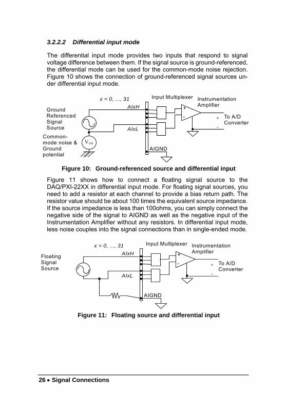
3.2.2.2 Differential input mode
The differential input mode provides two inputs that respond to signal voltage difference between them. If the signal source is ground-referenced, the differential mode can be used for the common-mode noise rejection. Figure 10 shows the connection of ground-referenced signal sources un-der differential input mode.
Figure 10: Ground-referenced source and differential input
Figure 11 shows how to connect a floating signal source to the DAQ/PXI-22XX in differential input mode. For floating signal sources, you need to add a resistor at each channel to provide a bias return path. The resistor value should be about 100 times the equivalent source impedance. If the source impedance is less than 100ohms, you can simply connect the negative side of the signal to AIGND as well as the negative input of the Instrumentation Amplifier without any resistors. In differential input mode, less noise couples into the signal connections than in single-ended mode.
AIxH
AIxL
x = 0, ..., 31
Floating Signal Source
To A/D Converter
AIGND
+-
InstrumentationAmplifier
+
-
Input Multiplexer
Figure 11: Floating source and differential input
AIxH
AIxL
x = 0, ..., 31
Ground Referenced Signal Source
To A/D Converter
AIGND
+-
InstrumentationAmplifier
Vcm
Common- mode noise & Ground potential
+
-
Input Multiplexer

28 • Operation Theory
4
Operation Theory
The operation theory of the functions on the DAQ/PXI-22XX is described in this chapter. The functions include the A/D conversion, D/A conversion, Digital I/O and General Purpose Counter / Timer. The operation theory can help you understand how to configure and program the DAQ/PXI-22XX.
4.1 A/D Conversion
When using an A/D converter, users should first know about the properties of the signal to be measured. Users can decide which channel to use and where to connect the signals to the card. Please refer to 3.2 for signal connections. In addition, users should define and control the A/D signal configurations, including channels, gains, and polarities (Unipolar/Bipolar).
The A/D acquisition is initiated by a trigger source; users must decide how to trigger the A/D conversion. The data acquisition will start once a trigger condition is matched.
After the end of an A/D conversion, the A/D data is buffered in a Data FIFO. The A/D data can now be transferred into the PC's memory for further processing.
Two acquisition modes, Software Polling and Scan acquisition are de-scribed below. Timing, trigger modes, trigger sources, and transfer meth-ods are included.
Operation Theory • 29
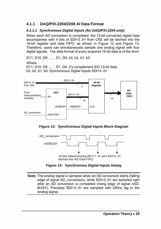
4.1.1 DAQ/PXI-2204/2208 AI Data Format 4.1.1.1 Synchronous Digital Inputs (for DAQ/PXI-2204 only) When each AD conversion is completed, the 12-bit converted digital data accompanied with 4 bits of SDI<3..0> from CN2 will be latched into the 16-bit register and data FIFO, as shown in Figure 12 and Figure 13. Therefore, users can simultaneously sample one analog signal with four digital signals. The data format of every acquired 16-bit data is of the form:
D11, D10, D9 ....... D1, D0, b3, b2, b1, b0 Where D11, D10, D9 ....... D1, D0: 2’s complement A/D 12-bit data b3, b2, b1, b0: Synchronous Digital Inputs SDI<3..0>
ADCAD<11..0>
16-bit Register
SDI<3..0> from CN2
From Instrumentation Amplifier
4
1216
ADData
FIFO Ain
SDI<3..0>
CLK nADBUSY
nADCONV AD_conversion
nADBUSY
Figure 12: Synchronous Digital Inputs Block Diagram
AD_conversion
nADBUSY
16 bits data(including AD<11..0> and SDI<3..0> latched into AD Data FIFO
Figure 13: Synchronous Digital Inputs timing
Note: The analog signal is sampled when an AD conversion starts (falling edge of signal AD_conversion), while SDI<3..0> are sampled right after an AD conversion is completed (rising edge of signal nAD-BUSY). Precisely SDI<3..0> are sampled with 280ns lag to the analog signal.
30 • Operation Theory
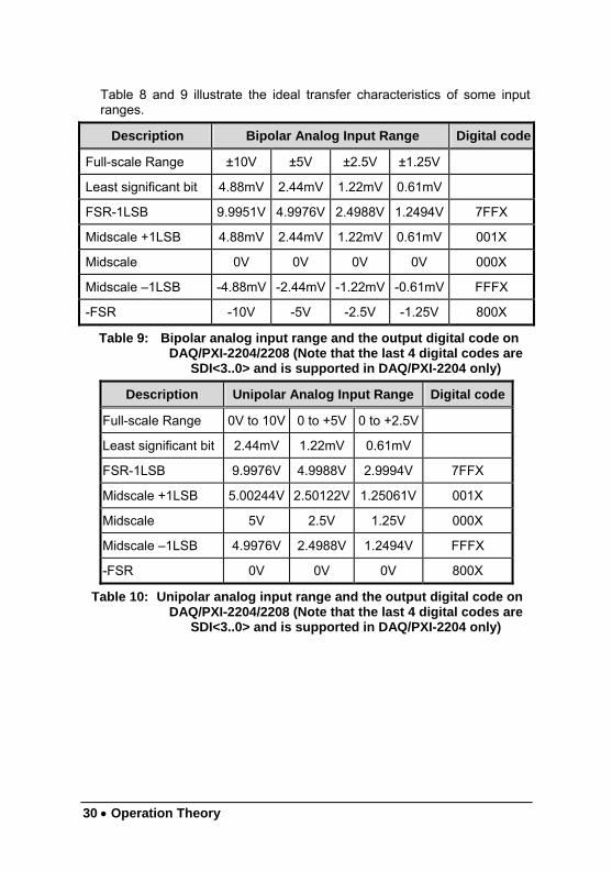
Table 8 and 9 illustrate the ideal transfer characteristics of some input ranges.
Description Bipolar Analog Input Range Digital code
Full-scale Range ±10V ±5V ±2.5V ±1.25V
Least significant bit 4.88mV 2.44mV 1.22mV 0.61mV
FSR-1LSB 9.9951V 4.9976V 2.4988V 1.2494V 7FFX
Midscale +1LSB 4.88mV 2.44mV 1.22mV 0.61mV 001X
Midscale 0V 0V 0V 0V 000X
Midscale –1LSB -4.88mV -2.44mV -1.22mV -0.61mV FFFX
-FSR -10V -5V -2.5V -1.25V 800X
Table 9: Bipolar analog input range and the output digital code on DAQ/PXI-2204/2208 (Note that the last 4 digital codes are
SDI<3..0> and is supported in DAQ/PXI-2204 only)
Description Unipolar Analog Input Range Digital code
Full-scale Range 0V to 10V 0 to +5V 0 to +2.5V
Least significant bit 2.44mV 1.22mV 0.61mV
FSR-1LSB 9.9976V 4.9988V 2.9994V 7FFX
Midscale +1LSB 5.00244V 2.50122V 1.25061V 001X
Midscale 5V 2.5V 1.25V 000X
Midscale –1LSB 4.9976V 2.4988V 1.2494V FFFX
-FSR 0V 0V 0V 800X
Table 10: Unipolar analog input range and the output digital code on DAQ/PXI-2204/2208 (Note that the last 4 digital codes are
SDI<3..0> and is supported in DAQ/PXI-2204 only)
Operation Theory • 31
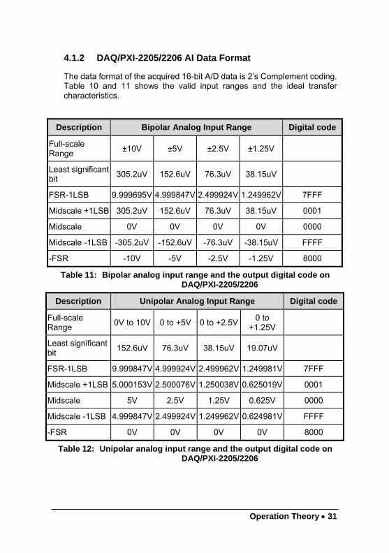
4.1.2 DAQ/PXI-2205/2206 AI Data Format
The data format of the acquired 16-bit A/D data is 2’s Complement coding. Table 10 and 11 shows the valid input ranges and the ideal transfer characteristics.
Description Bipolar Analog Input Range Digital code
Full-scale Range ±10V ±5V ±2.5V ±1.25V
Least significant bit 305.2uV 152.6uV 76.3uV 38.15uV
FSR-1LSB 9.999695V 4.999847V 2.499924V 1.249962V 7FFF
Midscale +1LSB 305.2uV 152.6uV 76.3uV 38.15uV 0001
Midscale 0V 0V 0V 0V 0000
Midscale -1LSB -305.2uV -152.6uV -76.3uV -38.15uV FFFF
-FSR -10V -5V -2.5V -1.25V 8000
Table 11: Bipolar analog input range and the output digital code on DAQ/PXI-2205/2206
Description Unipolar Analog Input Range Digital code
Full-scale Range 0V to 10V 0 to +5V 0 to +2.5V 0 to
+1.25V
Least significant bit 152.6uV 76.3uV 38.15uV 19.07uV
FSR-1LSB 9.999847V 4.999924V 2.499962V 1.249981V 7FFF
Midscale +1LSB 5.000153V 2.500076V 1.250038V 0.625019V 0001
Midscale 5V 2.5V 1.25V 0.625V 0000
Midscale -1LSB 4.999847V 2.499924V 1.249962V 0.624981V FFFF
-FSR 0V 0V 0V 0V 8000
Table 12: Unipolar analog input range and the output digital code on DAQ/PXI-2205/2206
32 • Operation Theory
4.1.3 Software conversion with polling data transfer acquisition mode (Software Polling)
This is the easiest way to acquire a single A/D data. The A/D converter starts one conversion whenever the dedicated software command is executed. Then the software would poll the conversion status and read the A/D data back when it is available.
This method is very suitable for applications that needs to process A/D data in real time. Under this mode, the timing of the A/D conversion is fully controlled under software. However, it is difficult to control the A/D con-version rate.
4.1.3.1 Specifying Channels, Gains, and input configurations in the Channel Gain Queue
In Software Polling and Programmable Scan Acquisition mode, the channel, gain, polarity, and input configuration (RSE, NRSE, or DIFF) can be specified in the Channel Gain Queue. You can fill the channel number in the Channel Gain Queue in any order. The channel order of acquisition will be the same as the order you set in the Channel Gain Queue. There-fore, you can acquire data with user-defined channel orders and with dif-ferent settings on each channel.
When the specified channels have been sampled from the first data to the last data in the Channel Gain Queue, the settings in Channel Gain Queue are maintained. You don’t need to re-configure the Channel Gain Queue if you want to keep on sampling data in the same order. The maximum number of entries you can set in the Channel Gain Queue is 512.
Example:
First you can set entries in Channel Gain Queue:
Ch3 with bipolar ±10V, RSE connection
Ch1 with bipolar ±2.5V, DIFF connection
Ch2 with unipolar 5V, NRSE connection
Ch1 with bipolar ±2.5V, DIFF connection
If you read 10 data by software polling method
Then the acquisition sequence of channels is: 3, 1, 2, 1, 3, 1, 2, 1, 3, 1
Operation Theory • 33
4.1.4 Programmable scan acquisition mode
4.1.4.1 Scan Timing and Procedure
It's recommended that this mode be used if your applications need a fixed and precise A/D sampling rate. You can accurately program the period between conversions of individual channels. There are at least 4 counters, which need to be specified:
SI_counter (24 bit): Specify the Scan Interval = SI_counter / Timebase
SI2_counter (16 bit): Specify the data Sampling Interval =
SI2_counter/Timebase
PSC_counter (24 bit): Specify Post Scan Counts after a trigger event
NumChan_counter (9 bit): Specify the Number of samples per scan
The acquisition timing and the meaning of the 4 counters are illustrated in figure 14
Timebase Clock Source
In scan acquisition mode, all the A/D conversions start on the output of counters, which use Timebase as the clock source. By software you can specify the Timebase to be either an internal clock source (on-board 40MHz) or an external clock input (EXTTIMEBASE) on CN2. The external clock is useful when you want to acquire data at rates not available with the internal A/D sample clock. The external clock source should generate TTL-compatible continuous clocks, and the maximum frequency is 40MHz while the minimum is 1MHz.

34 • Operation Theory
Figure 14: Scan Timing
There are 4 trigger modes to start the scan acquisition, please refer to 4.1.4.3 for the details. The data transfer mode will be discussed in 4.1.4.4.
Note:
1. The maximum A/D sampling rate is 3MHz for DAQ/PXI-2204/2208, 500kHz for DAQ/PXI-2205 and 250kHz for DAQ/PXI-2206. Therefore, the minimum setting for SI2_counter is 14 for DAQ/PXI-2204/2208, 80 for DAQ/PXI-2205 and 160 for DAQ/PXI-2206 while using the internal Timebase.
2. The SI_counter is a 24-bit counter and the SI2_counter is a 16-bit counter. Therefore, the maximum scan interval using the internal Timebase = 224/40M s = 0.419s, and the maximum sampling interval between 2 channels using the internal Timebase = 216/40M s = 1.638ms.
3. The scan interval can’t be smaller than the product of the data sam-pling interval and the NumChan_counter value. The relationship can be represented as: SI_counter>=SI2_counter * NumChan_counter.
Acquisition_in_progress
Scan_start
AD_conversion
Scan_in_progress (SSHOUT)(pin8 on CN2)
3 Scans, 4 Samples per scan (PSC_Counter=3, NumChan_Counter=4)
Sampling Interval t= SI2_COUNTER/TimeBase
Scan Interval T= SI_COUNTER/TimeBase
Ch2Ch3
Ch1Ch0
Ch2Ch3
Ch1Ch0
Ch2Ch3
Ch1Ch0
( channel sequences are specified in Channel Gain Queue)
Operation Theory • 35
Scan with SSH (DAQ/PXI-2208 doesn’t support this function)
You can send the SSHOUT signal on CN2 to an external S&H circuits to sample and hold all signals if you want to simultaneously sample all channels in a scan, as illustrated in Figure 14.
Note: The ‘SSHOUT’ signal is sent to external S&H circuits to hold the analog signal. Users must implement external S&H circuits on their own to carry out the S&H function. There are no on-board S&H circuits.
4.1.4.2 Specifying Channels, Gains, and input configurations in the Channel Gain Queue
Like software polling acquisition mode, the channel, gain, and input con-figurations can be specified in the Channel Gain Queue under the scan acquisition mode. Please refer to 4.1.3.1. Note that in scan acquisition mode the number of entries in the Channel Gain Queue is normally equivalent to the value of NumChan_counter (that is, the number of sam-ples per scan).
Example:
Set
SI2_counter = 160
SI_counter = 640
PSC_counter = 3
NumChan_counter = 4
Timebase = Internal clock source
Channel entries in the Channel Gain Queue: ch1, ch2, ch0, ch2
Then
Acquisition sequence of channels: 1, 2, 0, 2, 1, 2, 0, 2, 1, 2, 0, 2
Sampling Interval = 160/40M s = 4 us
Scan Interval = 640/40M s = 16 us
Equivalent sampling rate of ch0, ch1: 62.5kHz
Equivalent sampling rate of ch2: 125kHz
36 • Operation Theory
4.1.4.3 Trigger Modes
DAQ/PXI-22XX provides 3 trigger sources (internal software, external analog and digital trigger sources). You must select one of them as the source of the trigger event. A trigger event occurs when the specified condition is detected on the selected trigger source (For example, a rising edge on the external digital trigger input).
There are 4 trigger modes (pre-trigger, post-trigger, middle-trigger, and delay-trigger) working with the 4 trigger sources to initiate different scan data acquisition timing when a trigger event occurs. They are described as follows. For information of trigger sources, please refer to section 4.5.
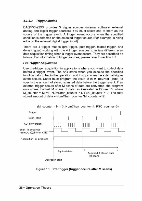
Pre-Trigger Acquisition
Use pre-trigger acquisition in applications where you want to collect data before a trigger event. The A/D starts when you execute the specified function calls to begin the operation, and it stops when the external trigger event occurs. Users must program the value M in M_counter (16bit) to specify the amount of stored scanned data before the trigger event. If an external trigger occurs after M scans of data are converted, the program only stores the last M scans of data, as illustrated in Figure 15, where M_counter = M =3, NumChan_counter =4, PSC_counter = 0. The total stored amount of data = NumChan_counter *M_counter =12.
Acquisition_in_progress
Scan_start
AD_conversion
Scan_in_progress (SSHOUT)(pin8 on CN2)
(M_counter = M = 3, NumChan_counter=4, PSC_counter=0)
Aquired dataAcquired & stored data (M scans)
Operation start
Trigger
Figure 15: Pre-trigger (trigger occurs after M scans)
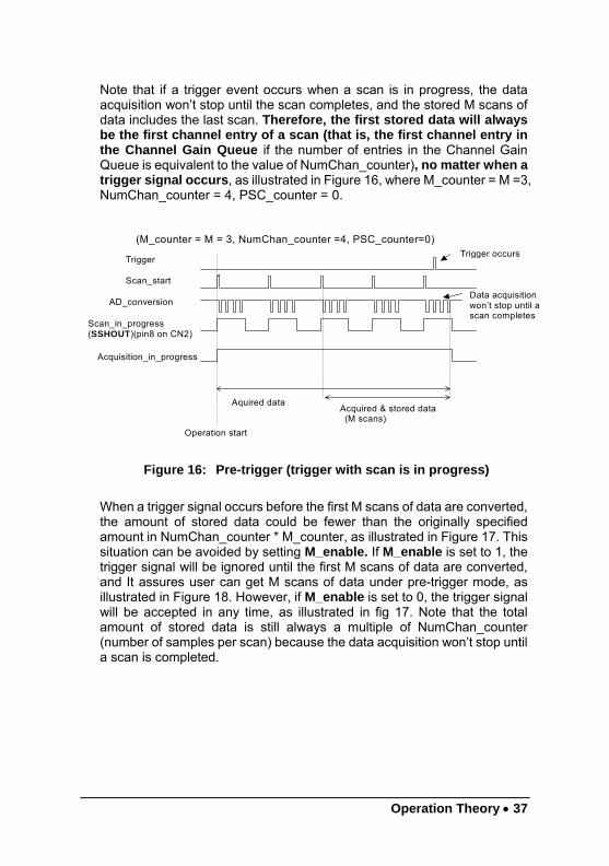
Operation Theory • 37
Note that if a trigger event occurs when a scan is in progress, the data acquisition won’t stop until the scan completes, and the stored M scans of data includes the last scan. Therefore, the first stored data will always be the first channel entry of a scan (that is, the first channel entry in the Channel Gain Queue if the number of entries in the Channel Gain Queue is equivalent to the value of NumChan_counter), no matter when a trigger signal occurs, as illustrated in Figure 16, where M_counter = M =3, NumChan_counter = 4, PSC_counter = 0.
Acquisition_in_progress
Scan_start
AD_conversion
Scan_in_progress (SSHOUT)(pin8 on CN2)
(M_counter = M = 3, NumChan_counter =4, PSC_counter=0)
Aquired dataAcquired & stored data (M scans)
Operation start
Trigger
Data acquisition won’t stop until a scan completes
Trigger occurs
Figure 16: Pre-trigger (trigger with scan is in progress)
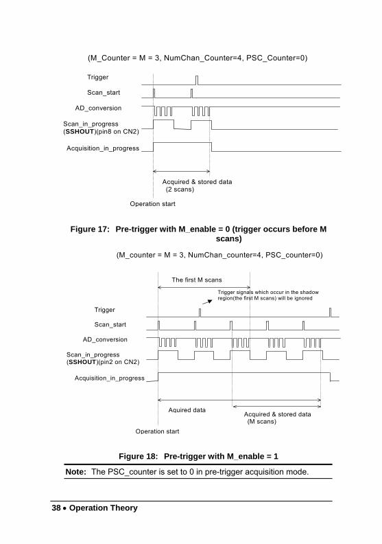
When a trigger signal occurs before the first M scans of data are converted, the amount of stored data could be fewer than the originally specified amount in NumChan_counter * M_counter, as illustrated in Figure 17. This situation can be avoided by setting M_enable. If M_enable is set to 1, the trigger signal will be ignored until the first M scans of data are converted, and It assures user can get M scans of data under pre-trigger mode, as illustrated in Figure 18. However, if M_enable is set to 0, the trigger signal will be accepted in any time, as illustrated in fig 17. Note that the total amount of stored data is still always a multiple of NumChan_counter (number of samples per scan) because the data acquisition won’t stop until a scan is completed.
38 • Operation Theory
Acquisition_in_progress
Scan_start
AD_conversion
Scan_in_progress (SSHOUT)(pin8 on CN2)
(M_Counter = M = 3, NumChan_Counter=4, PSC_Counter=0)
Acquired & stored data (2 scans)
Operation start
Trigger
Figure 17: Pre-trigger with M_enable = 0 (trigger occurs before M scans)
Acquisition_in_progress
Scan_start
AD_conversion
Scan_in_progress (SSHOUT)(pin2 on CN2)
(M_counter = M = 3, NumChan_counter=4, PSC_counter=0)
Aquired dataAcquired & stored data (M scans)
Trigger signals which occur in the shadow region(the first M scans) will be ignored
Operation start
Trigger
The first M scans
Figure 18: Pre-trigger with M_enable = 1
Note: The PSC_counter is set to 0 in pre-trigger acquisition mode.
Operation Theory • 39
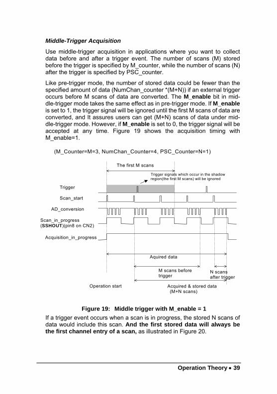
Middle-Trigger Acquisition
Use middle-trigger acquisition in applications where you want to collect data before and after a trigger event. The number of scans (M) stored before the trigger is specified by M_counter, while the number of scans (N) after the trigger is specified by PSC_counter.
Like pre-trigger mode, the number of stored data could be fewer than the specified amount of data (NumChan_counter *(M+N)) if an external trigger occurs before M scans of data are converted. The M_enable bit in mid-dle-trigger mode takes the same effect as in pre-trigger mode. If M_enable is set to 1, the trigger signal will be ignored until the first M scans of data are converted, and It assures users can get (M+N) scans of data under mid-dle-trigger mode. However, if M_enable is set to 0, the trigger signal will be accepted at any time. Figure 19 shows the acquisition timing with M_enable=1.
(M_Counter=M=3, NumChan_Counter=4, PSC_Counter=N=1)
Acquisition_in_progress
Scan_start
AD_conversion
Scan_in_progress (SSHOUT)(pin8 on CN2)
Aquired data
Acquired & stored data (M+N scans)
Operation start
Trigger
M scans before trigger
N scans after trigger
Trigger signals which occur in the shadow region(the first M scans) will be ignored
The first M scans
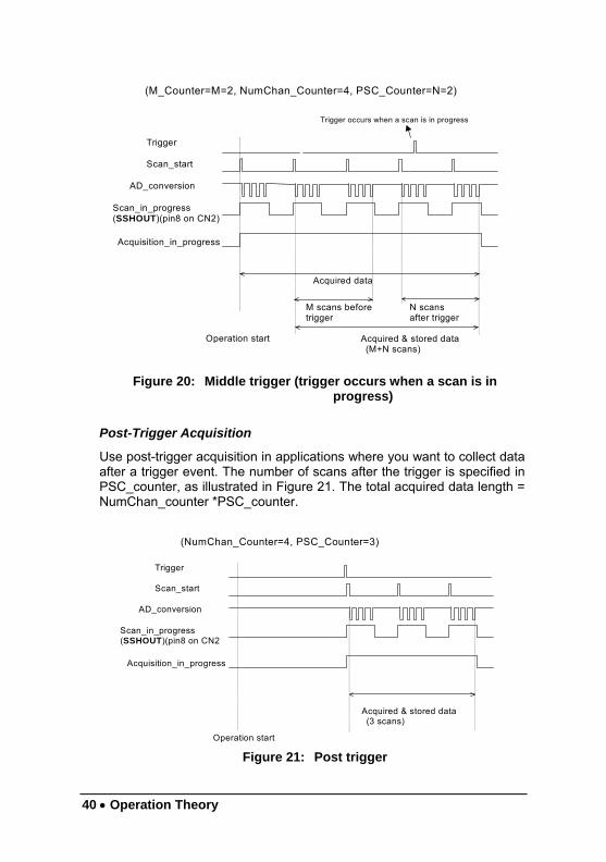
Figure 19: Middle trigger with M_enable = 1 If a trigger event occurs when a scan is in progress, the stored N scans of data would include this scan. And the first stored data will always be the first channel entry of a scan, as illustrated in Figure 20.
40 • Operation Theory
(M_Counter=M=2, NumChan_Counter=4, PSC_Counter=N=2)
Acquisition_in_progress
Scan_start
AD_conversion
Scan_in_progress (SSHOUT)(pin8 on CN2)
Acquired data
Acquired & stored data (M+N scans)
Trigger occurs when a scan is in progress
Operation start
Trigger
M scans before trigger
N scans after trigger
Figure 20: Middle trigger (trigger occurs when a scan is in progress)
Post-Trigger Acquisition
Use post-trigger acquisition in applications where you want to collect data after a trigger event. The number of scans after the trigger is specified in PSC_counter, as illustrated in Figure 21. The total acquired data length = NumChan_counter *PSC_counter.
(NumChan_Counter=4, PSC_Counter=3)
Acquisition_in_progress
Scan_start
AD_conversion
Scan_in_progress (SSHOUT)(pin8 on CN2
Acquired & stored data (3 scans)
Operation start
Trigger
Figure 21: Post trigger
Operation Theory • 41
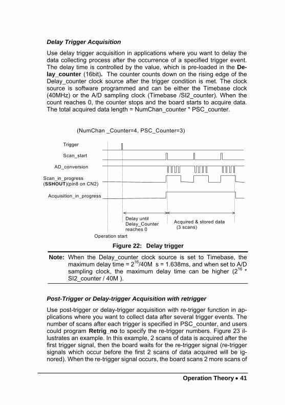
Delay Trigger Acquisition
Use delay trigger acquisition in applications where you want to delay the data collecting process after the occurrence of a specified trigger event. The delay time is controlled by the value, which is pre-loaded in the De-lay_counter (16bit). The counter counts down on the rising edge of the Delay_counter clock source after the trigger condition is met. The clock source is software programmed and can be either the Timebase clock (40MHz) or the A/D sampling clock (Timebase /SI2_counter). When the count reaches 0, the counter stops and the board starts to acquire data. The total acquired data length = NumChan_counter * PSC_counter.
(NumChan _Counter=4, PSC_Counter=3)
Acquisition_in_progress
Scan_start
AD_conversion
Scan_in_progress (SSHOUT)(pin8 on CN2)
Acquired & stored data (3 scans)
Operation start
Trigger
Delay until Delay_Counter reaches 0
Figure 22: Delay trigger
Note: When the Delay_counter clock source is set to Timebase, the maximum delay time = 216/40M s = 1.638ms, and when set to A/D sampling clock, the maximum delay time can be higher (216 * SI2_counter / 40M ).
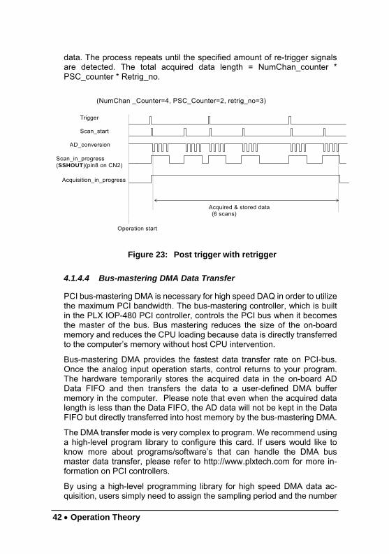
Post-Trigger or Delay-trigger Acquisition with retrigger
Use post-trigger or delay-trigger acquisition with re-trigger function in ap-plications where you want to collect data after several trigger events. The number of scans after each trigger is specified in PSC_counter, and users could program Retrig_no to specify the re-trigger numbers. Figure 23 il-lustrates an example. In this example, 2 scans of data is acquired after the first trigger signal, then the board waits for the re-trigger signal (re-trigger signals which occur before the first 2 scans of data acquired will be ig-nored). When the re-trigger signal occurs, the board scans 2 more scans of
42 • Operation Theory
data. The process repeats until the specified amount of re-trigger signals are detected. The total acquired data length = NumChan_counter * PSC_counter * Retrig_no.
(NumChan _Counter=4, PSC_Counter=2, retrig_no=3)
Acquisition_in_progress
Scan_start
AD_conversion
Scan_in_progress (SSHOUT)(pin8 on CN2)
Acquired & stored data (6 scans)
Operation start
Trigger
Figure 23: Post trigger with retrigger
4.1.4.4 Bus-mastering DMA Data Transfer
PCI bus-mastering DMA is necessary for high speed DAQ in order to utilize the maximum PCI bandwidth. The bus-mastering controller, which is built in the PLX IOP-480 PCI controller, controls the PCI bus when it becomes the master of the bus. Bus mastering reduces the size of the on-board memory and reduces the CPU loading because data is directly transferred to the computer’s memory without host CPU intervention.
Bus-mastering DMA provides the fastest data transfer rate on PCI-bus. Once the analog input operation starts, control returns to your program. The hardware temporarily stores the acquired data in the on-board AD Data FIFO and then transfers the data to a user-defined DMA buffer memory in the computer. Please note that even when the acquired data length is less than the Data FIFO, the AD data will not be kept in the Data FIFO but directly transferred into host memory by the bus-mastering DMA.
The DMA transfer mode is very complex to program. We recommend using a high-level program library to configure this card. If users would like to know more about programs/software’s that can handle the DMA bus master data transfer, please refer to http://www.plxtech.com for more in-formation on PCI controllers.
By using a high-level programming library for high speed DMA data ac-quisition, users simply need to assign the sampling period and the number
Operation Theory • 43
of conversion into their specified counters. After the AD trigger condition is matched, the data will be transferred to the system memory by the bus-mastering DMA.
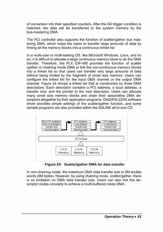
The PCI controller also supports the function of scatter/gather bus mas-tering DMA, which helps the users to transfer large amounts of data by linking all the memory blocks into a continuous linked list.
In a multi-user or multi-tasking OS, like Microsoft Windows, Linux, and so on, it is difficult to allocate a large continuous memory block to do the DMA transfer. Therefore, the PLX IOP-480 provides the function of scatter /gather or chaining mode DMA to link the non-continuous memory blocks into a linked list so that users can transfer very large amounts of data without being limited by the fragment of small size memory. Users can configure the linked list for the input DMA channel or the output DMA channel. Figure 24 shows a linked list that is constructed by three DMA descriptors. Each descriptor contains a PCI address, a local address, a transfer size, and the pointer to the next descriptor. Users can allocate many small size memory blocks and chain their associative DMA de-scriptors altogether by their application programs. DAQ/PXI-22XX software driver provides simple settings of the scatter/gather function, and some sample programs are also provided within the ADLINK all-in-one CD.
Figure 24: Scatter/gather DMA for data transfer
In non-chaining mode, the maximum DMA data transfer size is 2M double words (8M bytes). However, by using chaining mode, scatter/gather, there is no limitation on DMA data transfer size. Users can also link the de-scriptor nodes circularly to achieve a multi-buffered mode DMA.
44 • Operation Theory
4.2 D/A Conversion * DAQ/PXI-2208 doesn’t support this function.
There are 2 channels of 12-bit D/A output available in the DAQ/PXI-22XX. When using D/A converters, users should assign and control the D/A converter reference sources for the D/A operation mode and D/A channels. Users could also select the output polarity: unipolar or bipolar.
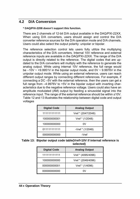
The reference selection control lets users fully utilize the multiplying characteristics of the D/A converters. Internal 10V reference and external reference inputs are available in the DAQ/PXI-22XX. The range of the D/A output is directly related to the reference. The digital codes that are up-dated to the D/A converters will multiply with the reference to generate the analog output. While using internal 10V reference, the full range would be –10V ~ +9.9951V in the bipolar output mode, and 0V ~ 9.9976V in the unipolar output mode. While using an external reference, users can reach different output ranges by connecting different references. For example, if connecting a DC –5V with the external reference, then the users can get a full range from –4.9976V to +5V in the bipolar output with inverting char-acteristics due to the negative reference voltage. Users could also have an amplitude modulated (AM) output by feeding a sinusoidal signal into the reference input. The range of the external reference should be within ±10V. Table 12 and 13 illustrates the relationship between digital code and output voltages
Digital Code Analog Output
111111111111 Vref * (2047/2048)
100000000001 Vref * (1/2048)
100000000000 0V
011111111111 -Vref * (1/2048)
000000000000 -Vref
Table 13: Bipolar output code table(Vref=10V if internal reference is selected)
Digital Code Analog Output
111111111111 Vref * (4095/4096)
100000000000 Vref * (2048/4096)
000000000001 Vref * (1/4096)
000000000000 0V
Operation Theory • 45
Table 14: Unipolar output code table (Vref=10V if internal reference is selected)
The D/A conversion is initiated by a trigger source. Users must decide how to trigger the D/A conversion. The data output will start when a trigger condition is met. Before the start of D/A conversion, D/A data is transferred from PC’s main memory to a buffering Data FIFO.
There are two modes of the D/A conversion: Software Update and Timed Waveform Generation are described, including timing, trigger source con-trol, trigger modes and data transfer methods. Either mode may be ap-plied to D/A channels independently. You can software update DA CH0 while generate timed waveforms on CH1 at the same time.
4.2.1 Software Update
This is the easiest way to generate D/A output. First, users should specify the D/A output channels, set output polarity: unipolar or bipolar, and ref-erence source: internal 10V or external AOEXTREF. Then update the digital values into D/A data registers through a software output command.
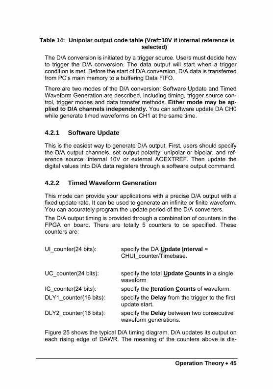
4.2.2 Timed Waveform Generation
This mode can provide your applications with a precise D/A output with a fixed update rate. It can be used to generate an infinite or finite waveform. You can accurately program the update period of the D/A converters. The D/A output timing is provided through a combination of counters in the FPGA on board. There are totally 5 counters to be specified. These counters are: UI_counter(24 bits): specify the DA Update Interval =
CHUI_counter/Timebase. UC_counter(24 bits): specify the total Update Counts in a single
waveform IC_counter(24 bits): specify the Iteration Counts of waveform. DLY1_counter(16 bits): specify the Delay from the trigger to the first
update start. DLY2_counter(16 bits): specify the Delay between two consecutive
waveform generations.
Figure 25 shows the typical D/A timing diagram. D/A updates its output on each rising edge of DAWR. The meaning of the counters above is dis-
46 • Operation Theory
cussed more in the following sections. For more information of Timebase, please refer to 4.1.2.1.
(UC _Counter=4, IC_Counter=3)
4 update counts, 3 iterations
DAWR
WFG_in_progress
DA update_interval t= UI_Counter/Timebase
Operation start
Trigger
Delay until DLY1_Counter reaches 0
Delay until DLY2_Counter reaches 0
Output Waveform
Delay until DLY2_Counter reaches 0
0 2
4
-4
A single waveform
UC_Counter=4
IC_Counter = 3
Figure 25: Typical D/A timing of waveform generation (Assuming the data in the data buffer are 2V, 4V, -4V, 0V)
Note: The maximum D/A update rate is 1MHz. Therefore; the minimum setting of UI_counter is 40 while using the internal Timebase (40MHz).
Operation Theory • 47
4.2.2.1 Trigger Modes
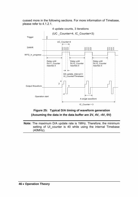
Post-Trigger Generation
Use post trigger when you want to perform DA waveform right after a trigger event occurs. In this trigger mode DLY1_Counter is not used and you don’t need to specify it. Figure 26 shows a single waveform generated right after a trigger signal is detected. The trigger signal could come from a software command, an analog trigger or a digital trigger. Please refer to section 4.5 for detailed information.
(UC _Counter=8, IC_Counter=1)
8 update counts, 1 iteration
DAWR
WFG_in_progress
Operation start
Trigger
Output Waveform 0
24
63
-4 -2
4
Figure 26: Post trigger waveform generation
(Assuming the data in the data buffer are 2V, 4V, 6V, 3V, 0V, -4V, -2V, 4V)
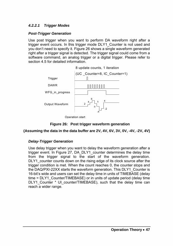
Delay-Trigger Generation
Use delay trigger when you want to delay the waveform generation after a trigger event. In Figure 27, DA_DLY1_counter determines the delay time from the trigger signal to the start of the waveform generation. DLY1_counter counts down on the rising edge of its clock source after the trigger condition is met. When the count reaches 0, the counter stops and the DAQ/PXI-22XX starts the waveform generation. This DLY1_Counter is 16-bit’s wide and users can set the delay time in units of TIMEBASE (delay time = DLY1_Counter/TIMEBASE) or in units of update period (delay time DLY1_Counter * UI_counter/TIMEBASE), such that the delay time can reach a wider range.
48 • Operation Theory
(UC _Counter=8, IC_Counter=1)
8 update counts, 1 iteration
DAWR
WFG_in_progress
Operation start
Trigger
Output Waveform
Delay until DLY1_counter reaches 0
Figure 27: Delay trigger waveform generation (Assuming the data in the data buffer are 2V, 4V, 6V, 3V, 0V, -4V, -2V, 4V)
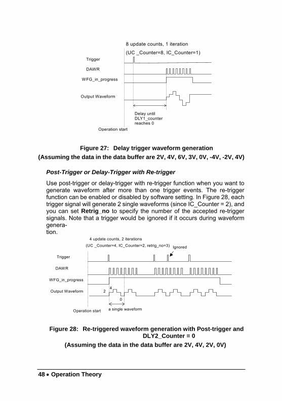
Post-Trigger or Delay-Trigger with Re-trigger
Use post-trigger or delay-trigger with re-trigger function when you want to generate waveform after more than one trigger events. The re-trigger function can be enabled or disabled by software setting. In Figure 28, each trigger signal will generate 2 single waveforms (since IC_Counter = 2), and you can set Retrig_no to specify the number of the accepted re-trigger signals. Note that a trigger would be ignored if it occurs during waveform genera-tion.
(UC _Counter=4, IC_Counter=2, retrig_no=3) 4 update counts, 2 iterations
Ignored
DAWR
WFG_in_progress
Operation start
Trigger
Output Waveform
0
2 4
a single waveform
Figure 28: Re-triggered waveform generation with Post-trigger and DLY2_Counter = 0
(Assuming the data in the data buffer are 2V, 4V, 2V, 0V)

Operation Theory • 49
4.2.2.2 Iterative Waveform Generation
Set IC_Counter in order to generate iterative waveforms from the data of a single waveform. The counter stores the iteration number, and the itera-tions could be finite (Figure 29) or infinite(Figure 30). Note that in infinite mode the waveform generation won’t stop until software stop function is executed, and IC_Counter is still meaningful when stop mode III is selected. Please refer to 4.2.2.3 for details.
A data FIFO on board is used to buffer the digital data for DA output. If the data size of a single waveform specified (That is, Update Counts in UC_Counter) is less than the FIFO size, after initially transferring the data from host PC memory to the FIFO on board, the data in FIFO will be automatically re-transmitted whenever a single waveform is completed. Therefore, it won’t occupy the PCI bandwidth when the iterative waveforms are performed. However, if the data size of a single waveform specified is more than the FIFO size, it needs to intermittently perform DMA to transfer data from host PC memory to the FIFO on board when the iterative waveforms are performed and occupies PCI bandwidth. The data FIFO size on the DAQ/PXI-22XX is 1024(words) when one DA channel is en-abled, and 512(words) when both DA channels are enabled.
(UC _Counter=4, IC_Counter=3)
4 update counts, 3 iterations
DAWR
WFG_in_progress
Operation start
Trigger
Output Waveform 0
24
A single waveform
Figure 29: Finite iterative waveform generation with Post-trigger and DLY2_Counter = 0
(Assuming the data in the data buffer are 2V, 4V, 2V, 0V)
50 • Operation Theory
(UC _Counter=4, IC_Counter=3) 4 update counts, infinite iterations
DAWR
WFG_in_progress
Operation start
Trigger
Output Waveform
waveform generation won’t stop until software stop function is executed
0
24
Figure 30: Infinite iterative waveform generation with Post-trigger and DLY2_Counter = 0
(Assuming the data in the data buffer are 2V, 4V, 2V, 0V)
Delay2 in iterative Waveform Generation
To stretch out the flexibility of the D/A waveform generation, we add a DLY2 Counter to separate 2 consecutive waveforms in iterative waveform generation. The time between two waveforms is assigned by setting the value of DLY2_Counter. The DLY2_Counter counts down after a complete waveform generation, and when it counts down to zero, the next waveform generation will start. This DLY2_Counter is 16-bits wide and users can set the delay time in the unit of Timebase (delay time = DLY2_Counter/Timebase) or in the unit of update period (delay time = DLY2_Counter * UI_Counter/Timebase), such that the delay time could reach a wide range.
4.2.2.3 Stop Modes of Scan Update
You can call software stop function to stop waveform generation when it is still in progress. Three stop modes are provided for timed waveform gen-eration, which means when is it to stop the waveform generation. You can apply these 3 modes to stop waveform generation no matter infinite or finite waveform generation mode is selected.
Figure 31 illustrates an example for stop mode I, in this mode the waveform stops immediately when software command is asserted.
In stop mode II, after a software stop command is given, the waveform generation won’t stop until a complete single waveform is finished. See figure 32 for an example, since UC_Counter is set to 4, the total DA up-dates counts (that is, number of pulses of DAWR signal) must be a multiple of 4 (update counts = 20 in this example).
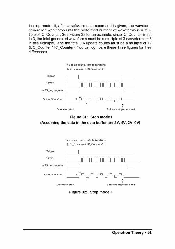
Operation Theory • 51
In stop mode III, after a software stop command is given, the waveform generation won’t stop until the performed number of waveforms is a mul-tiple of IC_Counter. See Figure 33 for an example, since IC_Counter is set to 3, the total generated waveforms must be a multiple of 3 (waveforms = 6 in this example), and the total DA update counts must be a multiple of 12 (UC_Counter * IC_Counter). You can compare these three figures for their differences.
(UC _Counter=4, IC_Counter=3) 4 update counts, infinite iterations
DAWR
WFG_in_progress
Operation start
Trigger
Output Waveform
0
24
Software stop command
Figure 31: Stop mode I (Assuming the data in the data buffer are 2V, 4V, 2V, 0V)
(UC _Counter=4, IC_Counter=3) 4 update counts, infinite iterations
DAWR
WFG_in_progress
Operation start
Trigger
Output Waveform
0
24
Software stop command
Figure 32: Stop mode II

52 • Operation Theory
(UC _Counter=4, IC_Counter=3) 4 update counts, infinite iterations
DAWR
WFG_in_progress
Operation start
Trigger
Output Waveform
0
24
Software stop command
Figure 33: Stop mode III
4.3 Digital I/O
DAQ/PXI-22XX contains 24-lines of general-purpose digital I/O (GPIO), which is provided through a 82C55A chip.
The 24-lines GPIO are separated into three ports: Port A, Port B and Port C. Port A, Port B, Port C high nibble (bit-4 to bit-7), and low nibble (bit 0 to bit 3) can be programmed to be input or output individually. At system startup and reset, all the I/O pins are all reset to be input configuration, that is, high impedance.
DAQ/PXI-2204 also provides 4 digital inputs (SDI from CN2), which are sampled simultaneously with the analog signal input and stored with the 12-bit AD data. Please refer to 4.1.1.1 for the details.
Operation Theory • 53
4.4 General Purpose Timer/Counter Operation * DAQ/PXI-2208 doesn’t support this function.
Two independent 16-bit up/down timer/counter are designed within FPGA for various applications. They have the following features:
• Count up/down controlled by hardware or software
• Programmable counter clock source (internal or external clock up to 10MHz)
• Programmable gate selection (hardware or software control)
• Programmable input and output signal polarities (high active or low active)
• Initial Count can be loaded from software
• Current count value can be read-back by software without affecting circuit operation
4.4.1 Timer/Counter functions basics
Each timer/counter has three inputs that can be controlled via hardware or software. They are clock input (GPTC_CLK), gate input (GPTC_GATE), and up/down control input (GPTC_UPDOWN). The GPTC_CLK input provides a clock source input to the timer/counter. Active edges on the GPTC_CLK input make the counter increment or decrement. The GPTC_UPDOWN input controls whether the counter counts up or down. The GPTC_GATE input is a control signal which acts as a counter enable or a counter trigger signal under different applications.
The output of timer/counter is GPTC_OUT. After power-up, GPTC_OUT is pulled high by a pulled-up resister about 10K ohms. Then GPTC_OUT goes low after the DAQ/PXI-22XX initialization.
All the polarities of input/output signals can be programmed by software. In this chapter, for easy explanation, all GPTC_CLK, GPTC_GATE, and GPTC_OUT are assumed to be active high or rising-edge triggered in the figures.
4.4.2 General Purpose Timer/Counter modes
Eight programmable timer/counter modes are provided. All modes start operating following a software-start signal that is set by the software. The GPTC software reset initializes the status of the counter and re-loads the initial value to the counter. The operation remains halted until the soft-

54 • Operation Theory
ware-start is re-executed. The operating theories under different modes are described as below. 4.4.2.1 Mode1: Simple Gated-Event Counting
In this mode, the counter counts the number of pulses on the GPTC_CLK after the software-start. Initial count can be loaded from software. Current count value can be read-back by software any time without affecting the counting. GPTC_GATE is used to enable/disable counting. When GPTC_GATE is inactive, the counter halts the current count value. Figure 34 illustrates the operation with initial count = 5, count-down mode.
55 4 3 2 1 1 0 ffff
Gate
CLK
Count value
Software start
Figure 34: Mode 1 Operation
4.4.2.2 Mode2: Single Period Measurement
In this mode, the counter counts the period of the signal on GPTC_GATE in terms of GPTC_CLK. Initial count can be loaded from software. After the software-start, the counter counts the number of active edges on GPTC_CLK between two active edges of GPTC_GATE. After the com-pletion of the period interval on GPTC_GATE, GPTC_OUT outputs high and then current count value can be read-back by software. Figure 35 il-lustrates the operation where initial count = 0, count-up mode.
00 1 2 3 4 5 5 5
Gate
CLK
Count value
Software start
Figure 35: Mode 2 Operation
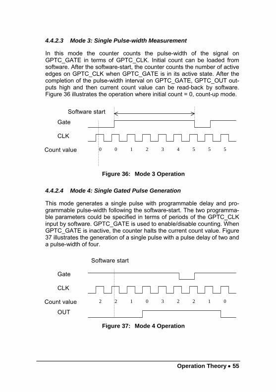
Operation Theory • 55
4.4.2.3 Mode 3: Single Pulse-width Measurement
In this mode the counter counts the pulse-width of the signal on GPTC_GATE in terms of GPTC_CLK. Initial count can be loaded from software. After the software-start, the counter counts the number of active edges on GPTC_CLK when GPTC_GATE is in its active state. After the completion of the pulse-width interval on GPTC_GATE, GPTC_OUT out-puts high and then current count value can be read-back by software. Figure 36 illustrates the operation where initial count = 0, count-up mode.
00 1 2 3 4 5 5 5
Gate
CLK
Count value
Software start
Figure 36: Mode 3 Operation
4.4.2.4 Mode 4: Single Gated Pulse Generation
This mode generates a single pulse with programmable delay and pro-grammable pulse-width following the software-start. The two programma-ble parameters could be specified in terms of periods of the GPTC_CLK input by software. GPTC_GATE is used to enable/disable counting. When GPTC_GATE is inactive, the counter halts the current count value. Figure 37 illustrates the generation of a single pulse with a pulse delay of two and a pulse-width of four.
22 1 0 3 2 2 1 0
Gate
CLK
Count value
OUT
Software start
Figure 37: Mode 4 Operation
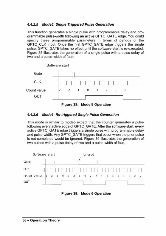
56 • Operation Theory
4.4.2.5 Mode5: Single Triggered Pulse Generation
This function generates a single pulse with programmable delay and pro-grammable pulse-width following an active GPTC_GATE edge. You could specify these programmable parameters in terms of periods of the GPTC_CLK input. Once the first GPTC_GATE edge triggers the single pulse, GPTC_GATE takes no effect until the software-start is re-executed. Figure 38 illustrates the generation of a single pulse with a pulse delay of two and a pulse-width of four.
22 1 0 3 2 1 0
Gate
CLK
Count value
OUT
Software start
Figure 38: Mode 5 Operation
4.4.2.6 Mode6: Re-triggered Single Pulse Generation
This mode is similar to mode5 except that the counter generates a pulse following every active edge of GPTC_GATE. After the software-start, every active GPTC_GATE edge triggers a single pulse with programmable delay and pulse-width. Any GPTC_GATE triggers that occur when the prior pulse is not completed would be ignored. Figure 39 illustrates the generation of two pulses with a pulse delay of two and a pulse-width of four.
22 1 0 3 2 1 0 2 2 1 0 3 2 1 0 2 2
G a t e
C L K
C o u n t v a l u e
O U T
S o f t w a r e s t a r t I g n o r e d
Figure 39: Mode 6 Operation
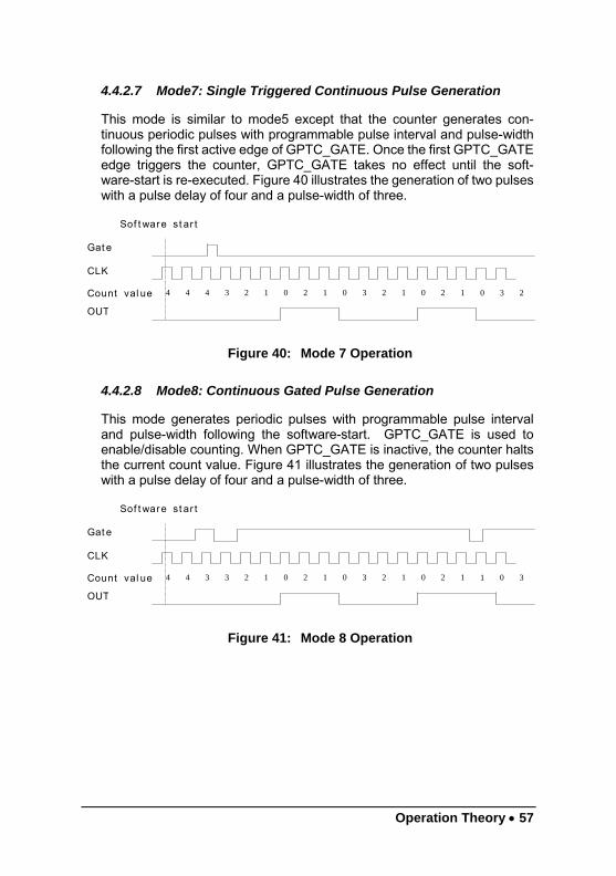
Operation Theory • 57
4.4.2.7 Mode7: Single Triggered Continuous Pulse Generation
This mode is similar to mode5 except that the counter generates con-tinuous periodic pulses with programmable pulse interval and pulse-width following the first active edge of GPTC_GATE. Once the first GPTC_GATE edge triggers the counter, GPTC_GATE takes no effect until the soft-ware-start is re-executed. Figure 40 illustrates the generation of two pulses with a pulse delay of four and a pulse-width of three.
44 4 3 2 1 0 2 1
S o f t w a r e s t a r t
0 3 2 1 0 2 1 0 3 2
G a t e
C L K
C o u n t v a l u e
O U T
Figure 40: Mode 7 Operation
4.4.2.8 Mode8: Continuous Gated Pulse Generation
This mode generates periodic pulses with programmable pulse interval and pulse-width following the software-start. GPTC_GATE is used to enable/disable counting. When GPTC_GATE is inactive, the counter halts the current count value. Figure 41 illustrates the generation of two pulses with a pulse delay of four and a pulse-width of three.
44 3 3 2 1 0 2 1
S o f t w a r e s t a r t
0 3 2 1 0 2 1 1 0 3
G a t e
C L K
C o u n t v a l u e
O U T
Figure 41: Mode 8 Operation

58 • Operation Theory
4.5 Trigger Sources
We provide flexible trigger selections in the DAQ/PXI-22XXseries products. In addition to the internal software trigger, DAQ/PXI-22XX also supports external analog, digital triggers and SSI triggers. Users can configure the trigger source by software for A/D and D/A processes individually. Note that the A/D and the D/A conversion share the same analog trigger.
4.5.1 Software-Trigger
This trigger mode does not need any external trigger source. The trigger asserts right after you execute the specified function calls to begin the operation. A/D and D/A processes can receive an individual software trigger.
4.5.2 External Analog Trigger
The analog trigger circuitry routing is shown in the Figure 42. The analog multiplexer could select either a direct analog input from the EXTATRIG pin (SRC1 in Figure 42) on the 68-pin connector CN1 or the input signal of ADC (SRC2 in Figure 42. That is, the first channel input you fill in the Channel Gain Queue). SRC1 can be used for all trigger modes while SRC2 can only be used for post and delay trigger modes. The range of trigger level for SRC1 is ±10V and the resolution is 78mV (please refer to Table 14, the valid code range is from 1 to 255), while the trigger range of SRC2 is the full-scale range of the first channel input in Channel Gain Queue, and the resolution is the desired range divided by 256. For example, if the first channel input in Channel Gain Queue is CH0 with bipolar ±5V range, the trigger voltage would be 4.96V when the trigger level code is set to 0xFF while –4.96V when the code is set to 0x01.
AIn
n = 0, ...,63
Instrumentation Amplifier A/D
Converter
Input MultipexerCN1
MUX Analog Trigger Circuit EXTATRIG SRC1
SRC2
Figure 42: Analog trigger block diagram

Operation Theory • 59
Trigger Level digital setting Trigger voltage
0xFF 9.92V
0xFE 9.84V
--- ---
0x81 0.08V
0x80 0
0x7F -0.08V
--- ---
0x01 -9.92V
Table 15: Analog trigger SRC1 (EXTATRIG) ideal transfer characteristic
The trigger signal is generated when the analog trigger condition is satis-fied. There are five analog trigger conditions in DAQ/PXI-22XX. DAQ/PXI-22XX uses 2 threshold voltages: Low_Threshold and High_ Threshold to build the 5 different trigger conditions. Users could configure the trigger conditions easily by software.
4.5.2.1 Below-Low analog trigger condition
Figure 43 shows the below-low analog trigger condition, the trigger signal is generated when the input analog signal is less than the Low_Threshold voltage, and the High_Threshold setting is not used in this trigger condi-tion.
Figure 43: Below-Low analog trigger condition
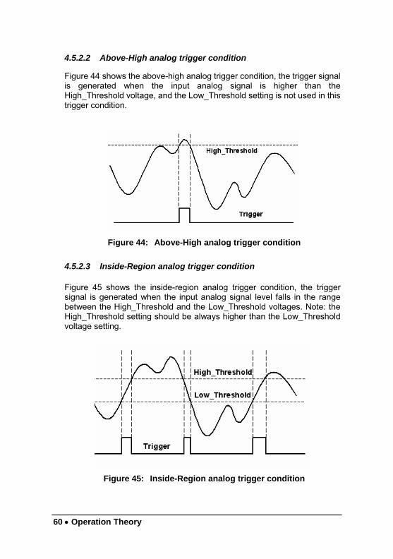
60 • Operation Theory
4.5.2.2 Above-High analog trigger condition
Figure 44 shows the above-high analog trigger condition, the trigger signal is generated when the input analog signal is higher than the High_Threshold voltage, and the Low_Threshold setting is not used in this trigger condition.
Figure 44: Above-High analog trigger condition
4.5.2.3 Inside-Region analog trigger condition
Figure 45 shows the inside-region analog trigger condition, the trigger signal is generated when the input analog signal level falls in the range between the High_Threshold and the Low_Threshold voltages. Note: the High_Threshold setting should be always higher than the Low_Threshold voltage setting.
Figure 45: Inside-Region analog trigger condition

Operation Theory • 61
4.5.2.4 High-Hysteresis analog trigger condition
Figure 46 shows the high-hysteresis analog trigger condition, the trigger signal is generated when the input analog signal level is greater than the High_Threshold voltage, and the Low_Threshold voltage determines the hysteresis duration. Note: the High_Threshold setting should be always higher than the Low_Threshold voltage setting.
Figure 46: High-Hysteresis analog trigger condition
4.5.2.5 Low-Hysteresis analog trigger condition
Figure 47 shows the low-hysteresis analog trigger condition, the trigger signal is generated when the input analog signal level is less than the Low_Threshold voltage, and the High_Threshold voltage determines the hysteresis duration. Note: the High_Threshold setting should be always higher than the Low_Threshold voltage setting.
Figure 47: Low-Hysteresis analog trigger condition
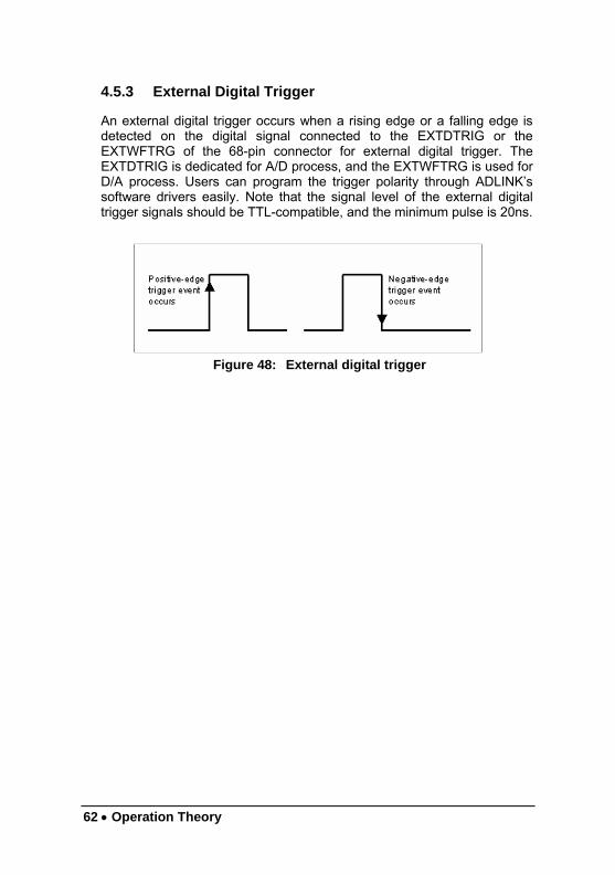
62 • Operation Theory
4.5.3 External Digital Trigger
An external digital trigger occurs when a rising edge or a falling edge is detected on the digital signal connected to the EXTDTRIG or the EXTWFTRG of the 68-pin connector for external digital trigger. The EXTDTRIG is dedicated for A/D process, and the EXTWFTRG is used for D/A process. Users can program the trigger polarity through ADLINK’s software drivers easily. Note that the signal level of the external digital trigger signals should be TTL-compatible, and the minimum pulse is 20ns.
Figure 48: External digital trigger
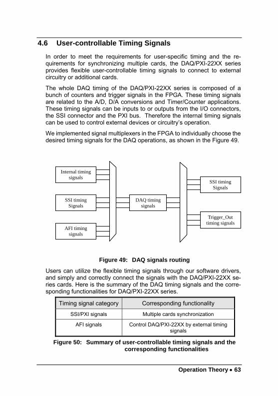
Operation Theory • 63
4.6 User-controllable Timing Signals
In order to meet the requirements for user-specific timing and the re-quirements for synchronizing multiple cards, the DAQ/PXI-22XX series provides flexible user-controllable timing signals to connect to external circuitry or additional cards.
The whole DAQ timing of the DAQ/PXI-22XX series is composed of a bunch of counters and trigger signals in the FPGA. These timing signals are related to the A/D, D/A conversions and Timer/Counter applications. These timing signals can be inputs to or outputs from the I/O connectors, the SSI connector and the PXI bus. Therefore the internal timing signals can be used to control external devices or circuitry’s operation.
We implemented signal multiplexers in the FPGA to individually choose the desired timing signals for the DAQ operations, as shown in the Figure 49.
Internal timing
signals
SSI timing Signals
AFI timing signals
DAQ timing signals
SSI timing Signals
Trigger_Out timing signals
Figure 49: DAQ signals routing
Users can utilize the flexible timing signals through our software drivers, and simply and correctly connect the signals with the DAQ/PXI-22XX se-ries cards. Here is the summary of the DAQ timing signals and the corre-sponding functionalities for DAQ/PXI-22XX series.
Timing signal category Corresponding functionality
SSI/PXI signals Multiple cards synchronization
AFI signals Control DAQ/PXI-22XX by external timing signals
Figure 50: Summary of user-controllable timing signals and the corresponding functionalities
64 • Operation Theory
4.6.1 DAQ timing signals
* SCAN_START, ADCONV and DA_TRIG, DAWR are supported by DAQ/PXI-2208.
The user-controllable DAQ timing-signals contains: (Please refer to 4.1.4.1 for the internal timing signal definition)
1. TIMEBASE, providing TIMEBASE for all DAQ operations, which could be from internal 40MHz oscillator, EXTTIMEBASE from I/O connector or the SSI_TIMEBASE. Note that the frequency range of the EXTTIMEBASE is 1MHz to 40MHz, and the EXTTIMEBASE should be TTL-compatible.
2. AD_TRIG, the trigger signal for the A/D operation, which could come from external digital trigger, analog trigger, internal software trigger and SSI_AD_TRIG. Refer to Section 4.5 for detailed description.
3. SCAN_START, the signal to start a scan, which would bring the following ADCONV signals for AD conversion, and could come from the internal SI_counter, AFI[0] and SSI_AD_START. This signal is synchronous to the TIMEBASE. Note that the AFI[0] should be TTL-compatible and the minimum pulse width should be the pulse width of the TIMEBASE to guarantee correct functionalities.
4. ADCONV, the conversion signal to initiate a single conversion, which could be derived from internal counter, AFI[0] or SSI_ADCONV. Note that this signal is edge-sensitive. When using AFI[0] as the external ADCONV source, each rising edge of AFI[0] would bring an effective conversion signal. Also note that the AFI[0] signal should be TTL-compatible and the minimum pulse width is 20ns.
5. DA_TRIG, the trigger signal for the D/A operation, which could be derived from external digital trigger, analog trigger, internal software trigger and SSI_AD_TRIG. Refer to Section 4.5 for detailed de-scription.
6. DAWR, the update signal to initiate a single D/A conversion, which could be derived from internal counter, AFI[1] or SSI_DAWR. Note that this signal is edge-sensitive. When using AFI[1] as the external DAWR source, each rising edge of AFI[1] would bring an effective update signal. Also note that the AFI[1] signal should be TTL-compatible and the minimum pulse width is 20ns.
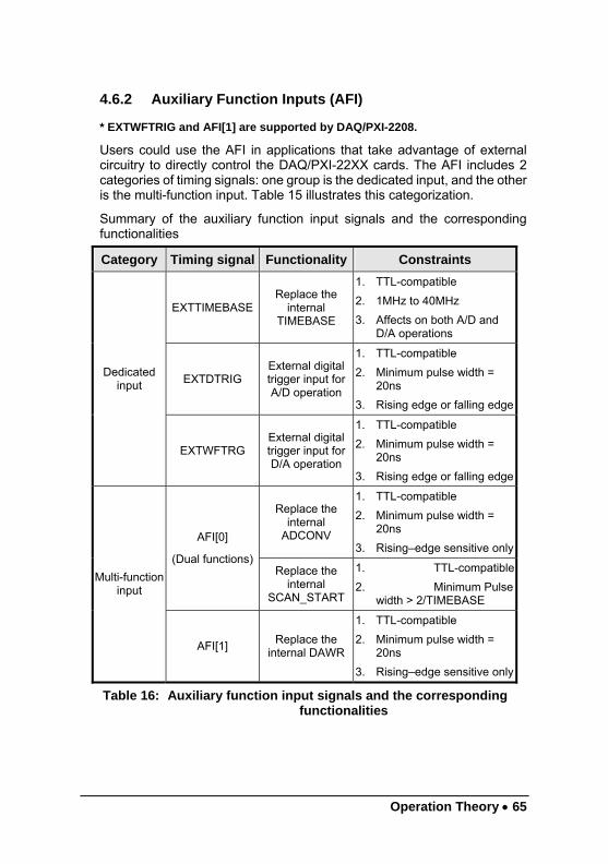
Operation Theory • 65
4.6.2 Auxiliary Function Inputs (AFI)
* EXTWFTRIG and AFI[1] are supported by DAQ/PXI-2208.
Users could use the AFI in applications that take advantage of external circuitry to directly control the DAQ/PXI-22XX cards. The AFI includes 2 categories of timing signals: one group is the dedicated input, and the other is the multi-function input. Table 15 illustrates this categorization.
Summary of the auxiliary function input signals and the corresponding functionalities
Category Timing signal Functionality Constraints
EXTTIMEBASEReplace the
internal TIMEBASE
1. TTL-compatible 2. 1MHz to 40MHz 3. Affects on both A/D and
D/A operations
EXTDTRIG External digital trigger input for A/D operation
1. TTL-compatible 2. Minimum pulse width =
20ns 3. Rising edge or falling edge
Dedicated input
EXTWFTRG External digital trigger input for D/A operation
1. TTL-compatible 2. Minimum pulse width =
20ns 3. Rising edge or falling edge
Replace the internal
ADCONV
1. TTL-compatible 2. Minimum pulse width =
20ns 3. Rising–edge sensitive only
AFI[0]
(Dual functions)Replace the
internal SCAN_START
1. TTL-compatible2. Minimum Pulse
width > 2/TIMEBASE
Multi-function input
AFI[1] Replace the internal DAWR
1. TTL-compatible 2. Minimum pulse width =
20ns 3. Rising–edge sensitive only
Table 16: Auxiliary function input signals and the corresponding functionalities
66 • Operation Theory
EXTDTRIG and EXTWFTRIG
EXTDTRIG and EXTWFTRIG are dedicated digital trigger input signals for A/D and D/A operations respectively. Please refer to section 4.5.3 for de-tailed descriptions.
EXTTIMEBASE
When the applications needs specific sampling frequency or update rate that the card could not generate from its internal TIMEBASE, the 40MHz clock, users could utilize the EXTTIMEBASE with internal counters to achieve the specific timing intervals for both A/D and D/A operations. Note that once you choose the TIMEBASE source, both A/D and D/A operations will be affected because A/D and D/A operations share the same TIMEBASE
AFI[0]
Alternatively, users can also directly apply an external A/D conversion signal to replace the internal ADCONV signal. This is another way to achieve customized sampling frequencies. The external ADCONV signal can only be inputted from the AFI[0]. As section 4.1 describes, the SI_counter triggers the generation of the A/D conversion signal, ADCONV, but when using the AFI[0] to replace the internal ADCONV signal, then the SI_counter and the internally generated SCAN_START will not be effective. By controlling the ADCONV externally, users can sample the data ac-cording to external events. In this mode, the Trigger signal and trigger mode settings will are not available. AFI[0] could also be used as SCAN_START signal for A/D operations. Please refer to sections 4.1 and 4.6.1 for detailed descriptions of the SCAN_START signal. When using external signal (AFI[0]) to replace the internal SCAN_START signal, the pulse width of the AFI[0] must be greater than two time of the period of Timebase. This feature is suitable for the DAQ-2200/PXI-2200 series, which can scan multiple channels data con-trolled by an external event. Note that the AFI[0] is a multi-purpose input, and it can only be utilized for one function at any one time.
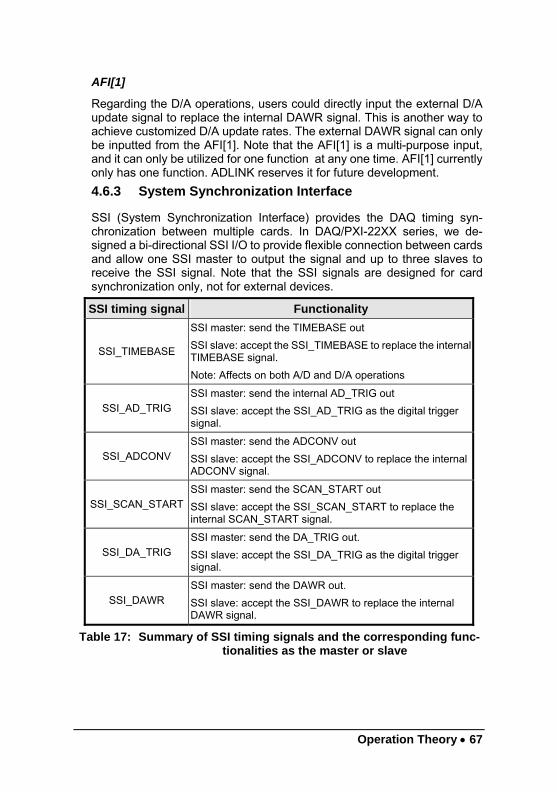
Operation Theory • 67
AFI[1]
Regarding the D/A operations, users could directly input the external D/A update signal to replace the internal DAWR signal. This is another way to achieve customized D/A update rates. The external DAWR signal can only be inputted from the AFI[1]. Note that the AFI[1] is a multi-purpose input, and it can only be utilized for one function at any one time. AFI[1] currently only has one function. ADLINK reserves it for future development. 4.6.3 System Synchronization Interface
SSI (System Synchronization Interface) provides the DAQ timing syn-chronization between multiple cards. In DAQ/PXI-22XX series, we de-signed a bi-directional SSI I/O to provide flexible connection between cards and allow one SSI master to output the signal and up to three slaves to receive the SSI signal. Note that the SSI signals are designed for card synchronization only, not for external devices.
SSI timing signal Functionality
SSI_TIMEBASE
SSI master: send the TIMEBASE out SSI slave: accept the SSI_TIMEBASE to replace the internal TIMEBASE signal. Note: Affects on both A/D and D/A operations
SSI_AD_TRIG SSI master: send the internal AD_TRIG out SSI slave: accept the SSI_AD_TRIG as the digital trigger signal.
SSI_ADCONV SSI master: send the ADCONV out SSI slave: accept the SSI_ADCONV to replace the internal ADCONV signal.
SSI_SCAN_STARTSSI master: send the SCAN_START out SSI slave: accept the SSI_SCAN_START to replace the internal SCAN_START signal.
SSI_DA_TRIG SSI master: send the DA_TRIG out. SSI slave: accept the SSI_DA_TRIG as the digital trigger signal.
SSI_DAWR SSI master: send the DAWR out. SSI slave: accept the SSI_DAWR to replace the internal DAWR signal.
Table 17: Summary of SSI timing signals and the corresponding func-tionalities as the master or slave
68 • Operation Theory
In PCI form factor, there is a connector on the top right corner of the card for the SSI. Refer to section 2.3 for the connector position. All the SSI signals are routed to the 20-pin connector from the FPGA. To synchronize multiple cards, users can connect a special ribbon cable (ACL-SSI) to all the cards in a daisy-chain configuration
In PXI form factor, we utilize the PXI trigger bus built on the PXI backplane to provide the necessary timing signal connections. All the SSI signals are routed to the P2 connector. No additional cable is needed. For detailed information of the PXI specifications, please refer to PXI specification Re-vision 2.0 from PXI System Alliance (www.pxisa.org).
The 6 internal timing signals could be routed to the SSI or the PXI trigger bus through software drivers. Please refer to section 4.6.1 for detailed in-formation of the 6 internal timing signals. Physically the signal routings are accomplished in the FPGA. Cards that are connected together through the SSI or the PXI trigger bus, will still achieve synchronization on the 6 timing signals.
The mechanism of the SSI/PXI
1. We adopt master-slave configuration for SSI/PXI. In a system, for each timing signal, there shall be only one master, and other cards are SSI slaves or with the SSI function disabled.
2. For each timing signal, the SSI master doesn’t have to be in a single card.
For example:
We want to synchronize the A/D operation through the ADCONV signal for 4 DAQ/PXI-22XX cards. Card 1 is the master, and Card 2, 3, 4 are slaves. Card 1 receives an external digital trigger to start the post trigger mode acquisition. The SSI setting could be:
a. Set the SSI_ADCONV signal of Card 1 to be the master.
b. Set the SSI_ADCONV signals of Card 2, 3, 4 to be the slaves.
c. Set external digital trigger for Card 1’s A/D operation.
d. Set SI_counter, SI2_counter, NumChan_counter and the post scan counter (PSC) on all other cards.
e. Start DMA operations for all cards, thus all the cards are waiting for the trigger event.

Operation Theory • 69
When the digital trigger condition of Card 1 occurs, Card 1 will internally generate the ADCONV signal and output this ADCONV signal to SSI_ADCONV signal of Card 2, 3 and 4 through the SSI/PXI connectors. Thus we can achieve simultaneous acquisition across four modules .
You could arbitrarily choose each of the 6 timing signals as the SSI master from any one of the cards. The SSI master can output the internal timing signals to the SSI slaves. With the SSI, users could achieve better card-to-card synchronization.
Note that when power-up or reset, the DAQ timing signals are reset to use the internal generated timing signals.
70 • Calibration
5
Calibration
This chapter introduces the calibration process to minimize AD meas-urement errors and DA output errors.
5.1 Loading Calibration Constants
The DAQ/PXI-22XX is factory calibrated before shipment by writing the associated calibration constants of TrimDACs to the on-board EEPROM. TrimDACs are devices containing multiple DACs within a single package. TrimDACs do not have memory capability. That means the calibration constants do not retain their values after the system power is turned off. Loading calibration constants is the process of loading the values of TrimDACs stored in the on-board EEPROM. ADLINK provides software to make it easy to read the calibration constants automatically when neces-sary.
There is a dedicated space for calibration constants In the EEPROM. In addition to the default bank of factory calibration constants, there are three extra user-modifiable banks. This means users can load the TrimDACs values either from the original factory calibration or from a calibration that is subsequently performed.
Because of the fact that errors in measurements and outputs will vary with time and temperature, it is recommended re-calibratation when the card is installed in the users environment. The auto-calibration function used to minimize errors will be introduced in the next sub-section.
Calibration • 71
5.2 Auto-calibration
By using the auto-calibration feature of the DAQ/PXI-22XX, the calibration software can measure and correct almost all the calibration errors without any external signal connections, reference voltages, or measurement de-vices.
The DAQ/PXI-22XX has an on-board calibration reference to ensure the accuracy of auto-calibration. The reference voltage is measured at the factory and adjusted through a digital potentiometer by using an ul-tra-precision calibrator. The impedance of the digital potentiometer is memorized after this adjustment. It is not recommended for users to adjust the on-board calibration reference except when an ultra-precision cali-brator is available.
Note: 1. Before auto-calibration procedure starts, it is recommended to
warn up the card for at least 15 minutes.
2. Please remove the cable before an auto-calibration procedure is initiated because the DA outputs would be changed in the process of calibration.
5.3 Saving Calibration Constants
After an auto-calibration is completed, users can save the new calibration constants into one of the three user-modifiable banks in the EEPROM. The date and the temperature when you ran the auto-calibration will be saved accompanied with the calibration constants. This means users can store three sets of calibration constants according to three different environ-ments and re-load the calibration constants later.
.

72 • Warranty Policy
Warranty Policy Thank you for choosing ADLINK. To understand your rights and enjoy all the after-sales services we offer, please read the following carefully:
1. Before using ADLINK’s products please read the user manual and follow the instructions exactly.
2. When sending in damaged products for repair, please attach an RMA application form.
3. All ADLINK products come with a two-year guarantee, repaired free of charge.
• The warranty period starts from the product’s shipment date from ADLINK’s factory.
• Peripherals and third-party products not manufactured by ADLINK will be covered by the original manufacturers’ warranty.
• End users requiring maintenance services should contact their local dealers. Local warranty conditions will depend on local dealers.
4. This warranty will not cover repair costs due to:
• Damage caused by not following instructions. • Damage caused by carelessness on the users’ part during product
transportation. • Damage caused by fire, earthquakes, floods, lightening, pollution,
other acts of God, and/or incorrect usage of voltage transformers. • Damage caused by unsuitable storage environments (i.e. high tem-
peratures, high humidity, or volatile chemicals. • Damage caused by leakage of battery fluid. • Damage from improper repair by unauthorized technicians. • Products with altered and/or damaged serial numbers. • Other categories not protected under our guarantees.
5. Customers are responsible for shipping costs to transport damaged products to our company or sales office.
6. To ensure the speed and quality of product repair, please download a RMA application form from our company website: www.adlinktech.com. Damaged products with attached RMA forms receive priority.
For further questions, please contact our FAE staff.
ADLINK: [email protected]


![AMENDMENT NO. llll lll - Steptoe & Johnson3 O:\HEN\HEN20312.xml [file 1 of 2] S.L.C. Sec. 2205. Modification of limitations on charitable contributions during 2020. Sec. 2206. Exclusion](https://static.fdocuments.in/doc/165x107/5f911aa13d0dc325eb6f5432/amendment-no-llll-lll-steptoe-3-ohenhen20312xml-file-1-of-2-slc.jpg)


![AMENDMENT NO. llll lll...3 O:\HEN\HEN20312.xml [file 1 of 2] S.L.C. Sec. 2205. Modification of limitations on charitable contributions during 2020. Sec. 2206. Exclusion for certain](https://static.fdocuments.in/doc/165x107/5f0d09087e708231d4385b40/amendment-no-llll-lll-3-ohenhen20312xml-file-1-of-2-slc-sec-2205.jpg)


![Original Article High intensity focused ultrasound inhibits breast cancer … · 2020. 4. 27. · HIFU inhibits breast cancer 2206 Int J Clin Exp Med 2020;13(4):2205-2215 [10]. Moreover,](https://static.fdocuments.in/doc/165x107/6002df81a9e7ac55f44947b9/original-article-high-intensity-focused-ultrasound-inhibits-breast-cancer-2020.jpg)