Nuances in Ultra-Low Power Designs for Wearable Products Low Power... · Nuances in Ultra-Low Power...
21
1 Nuances in Ultra-Low Power Designs for Wearable Products Steven Schnier and Chris Glaser March 2016
Transcript of Nuances in Ultra-Low Power Designs for Wearable Products Low Power... · Nuances in Ultra-Low Power...
1
Nuances in Ultra-Low Power Designs for Wearable Products
Steven Schnier and Chris Glaser
March 2016

Why is Low Power Needed?
• Wearables consist of many
functions
– Small Battery with Charger
– Display (AMOLED, PMOLED,
LCD, eInk, etc.)
– Radio (BLE, WLAN, LTEM,
etc.)
– MCU (microcontroller to
mobile chipset)
– Sensors (6-axis sensor,
temperature, humidity, light,
heart rate, etc)
– Vibration Motor
• How long the battery lasts
depends on carefully
managing each function
2
Host MCU
Charger
Bluetooth
LE
Sensors
Display
Li-Ion Battery
DC/DC
BuckLDO
I2C
5V Wall Adapter
DC/DC
Boost
VBAT
Monitor
Push-
Button
Controller
BAT
FET
DC/DC
Boost
HRM LED
Why is Low Power Needed?
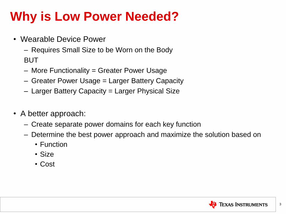
• Wearable Device Power
– Requires Small Size to be Worn on the Body
BUT
– More Functionality = Greater Power Usage
– Greater Power Usage = Larger Battery Capacity
– Larger Battery Capacity = Larger Physical Size
• A better approach:
– Create separate power domains for each key function
– Determine the best power approach and maximize the solution based on
• Function
• Size
• Cost
3
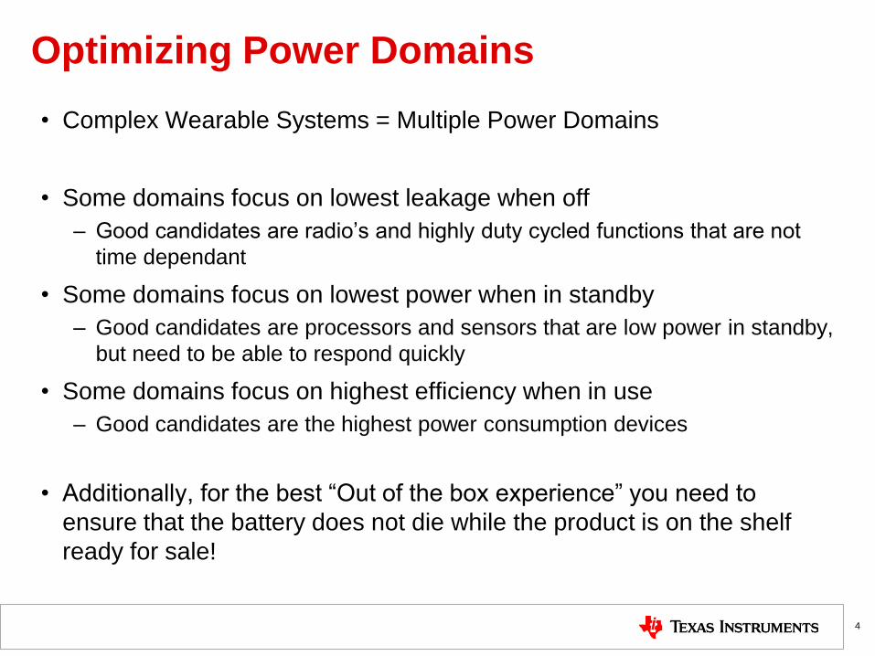
Optimizing Power Domains
• Complex Wearable Systems = Multiple Power Domains
• Some domains focus on lowest leakage when off
– Good candidates are radio’s and highly duty cycled functions that are not
time dependant
• Some domains focus on lowest power when in standby
– Good candidates are processors and sensors that are low power in standby,
but need to be able to respond quickly
• Some domains focus on highest efficiency when in use
– Good candidates are the highest power consumption devices
• Additionally, for the best “Out of the box experience” you need to
ensure that the battery does not die while the product is on the shelf
ready for sale!
4

Low Off Current – Ship Mode
• Choose an architecture that
can disconnect the battery from
the rest of the system for the
lowest leakage when the
device is being shipped or on
the shelf
• Power Path chargers have a
BAT FET that enables this
function to ~2nA at room temp!
5
Example: bq25120

Low Off Current – True Disconnect Switch
• When a sub-system is ‘off’ you want 0 current consumption
– This is not physically possible – some nA always remain
• All systems have leakage currents
– This is the current consumed when it is ‘off’
• Different DC/DC topologies have different leakage paths
6
Buck Boost
Leakage is mainly in high-side FET Leakage is in low-side FET
and to output!

Removing boost converter leakage TPS61046 contains an internal isolation switch to separate Vin from Vout

Low Off Current – Load Switch
• For devices that don’t have
load disconnect switches, a
load switch can provide the
same function
• Standalone load switches can
be used, or they can be
integrated into a larger battery
management IC
• The bq25120 has a load switch
that can be configured as a
regulated LDO output if needed
• The input can be run from the
battery, or from the DC/DC
converter to optimize efficiency
8
Example: bq25120
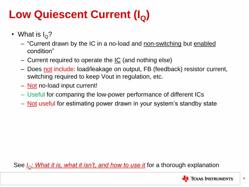
Low Quiescent Current (IQ)
• What is IQ?
– “Current drawn by the IC in a no-load and non-switching but enabled
condition”
– Current required to operate the IC (and nothing else)
– Does not include: load/leakage on output, FB (feedback) resistor current,
switching required to keep Vout in regulation, etc.
– Not no-load input current!
– Useful for comparing the low-power performance of different ICs
– Not useful for estimating power drawn in your system’s standby state
9
See IQ: What it is, what it isn’t, and how to use it for a thorough explanation

Buck IQ
• Almost always drawn from Vin
• TPS62743 IQ specification:
• For a buck, no-load input current is usually slightly greater than IQ
• Do you have no load or just a very light load (some µA or 100s of nA)?
10
IC enabled
True IQ (non-switching)
No-load input current (IC switching)

The power of an ultra-low IQ buck
11
TPS62125: 13 µA IQ TPS62743: 360 nA IQ
50% efficiency at 30 µA load 91% efficiency at 30 µA load 50% efficiency at < 1 µA load!

Boost IQ
• Some drawn from Vin but usually some drawn from Vout as well
– Vout’s IQ ultimately comes from Vin creates higher no-load input current
• TPS61220 IQ specification:
• Resulting no-load input current:
12
IC enabled
Most current is drawn from Vout!
No-load input current = 20 µA!!

High Efficiency at Full Load
• Light load efficiency is dependant on Iq and switching losses
• Full load efficiency is dependant on
– The ratio of input and output voltages
– The resistance of the FET from drain to source (RDSON) when conducting
– The DCR of the inductor
13
Example: bq25120 using inductor with 240mΩ DCR

Wearables Solutions Coverage
• bq25120
Meets all basic
functional
requirements
Smallest Solution
Size and Lowest
Power Consumption
14
• bq25120
• Add TPS61046
boost for display
• Add TPS62743 buck
if needed
Most Flexible Solution
• bq25120
• Add TPS62770
for boost and
buck and current
sink
Smallest Solution
for Full Featured
Applications
Activity Monitor Activity Monitor
With Display
Activity Monitor
With Display and
Additional Features
Sports Watch
With Display and
Full Featured
• bq2510x Smallest Linear
Charger
• TPS62743 Smallest Low Iq
DC/DC Converter
Smallest Solution IF
power path and I2C
configurability is not
needed
Audio Devices

bq25120: Battery Management for Wearables
• Fitness Accessories
• Smart Watches and other Wearable Devices
• Health Monitoring Medical Accessories
• Rechargeable Toys
15
Low Iq Linear Charger with Power Path Management, PWM Output, Load Switch, Voltage Based
Battery Monitor, and Push-Button Reset
Applications
Features
1. Low battery current draw (Iq)
< 750nA (typ) BAT Iq with 1.8V Output Enabled
< 50nA (typ) BAT Iq in Shipmode
Low Iq allows wearables to be always-on without
draining the battery. Shipmode allows shipping the
device with the longest battery shelf life.
2. Small size
2.5mm x 2.5mm WCSP Package
15 mm² solution size (components)
3. Integration
Linear Charger: 300mA, 3.4V-5.5V input, 20V max
LDO: 100mA
Buck Converter: 300mA, 2.2V- 6.6V input
Power path (switcher)
Load switch
pushbutton control
battery voltage monitor: Accurate 2% VBATREG
I2C programmable flexibility to set all key parameters
including ICHG, VBATREG, ITERM
BQ25120
Host MCU
Charger
Bluetooth
LE
Sensors
Display
Li-Ion Battery
DC/DC
BuckLDO
I2C
5V Wall Adapter
TPS61046
DC/DC
Boost
VBAT
Monitor
Push-
Button
Controller
BAT
FET
TPS61046
DC/DC
Boost
HRM LED

bq25120 – Application Schematic
For Radio,
Sensor,
Motor or
other
infrequently
used
functions
HOST can
control
CD, ILIM,
ITERM, ISET,
Hi-Z,
LS/LDO, SYS
VBATREG,
TIMER,
RESET,
VINDPM,
SHIPMODE
and see
STATUS and
FAULTS
Load Switch /
LDO input
For default and
non-HOST
Operation -
OPTIONAL
For temp sensing
- OPTIONAL
GND
HOST SDA
SCL
INT
SW
BAT
MR
BQ25120
MCU /
SYSTEM
-+
NTCTS
LS / LDO
<100mA
Load
IN
SYS
RESET
LSCTRL
VINLS
Unregulated
Load
PMIDPG
IPRETERM
ISET
ILIM
CD
IN

BQ25120
Host MCU
Charger
Bluetooth
LE
Sensors
Display
Li-Ion Battery
DC/DC
BuckLDO
I2C
5V Wall Adapter
TPS61046
DC/DC
Boost
VBAT
Monitor
Push-
Button
Controller
BAT
FET
TPS61240
DC/DC
Boost
HRM LED
Solution with bq25120 (PMP11311)
17
• bq25120
• bq51003 for Wireless Charging
• TPS61046 boost for OLED
display
• TPS61240 boost for Heart Rate
Monitor or LCD display
• TPS62743 buck
Most Flexible Solution
For Activity Monitor
With Display and
Additional Features
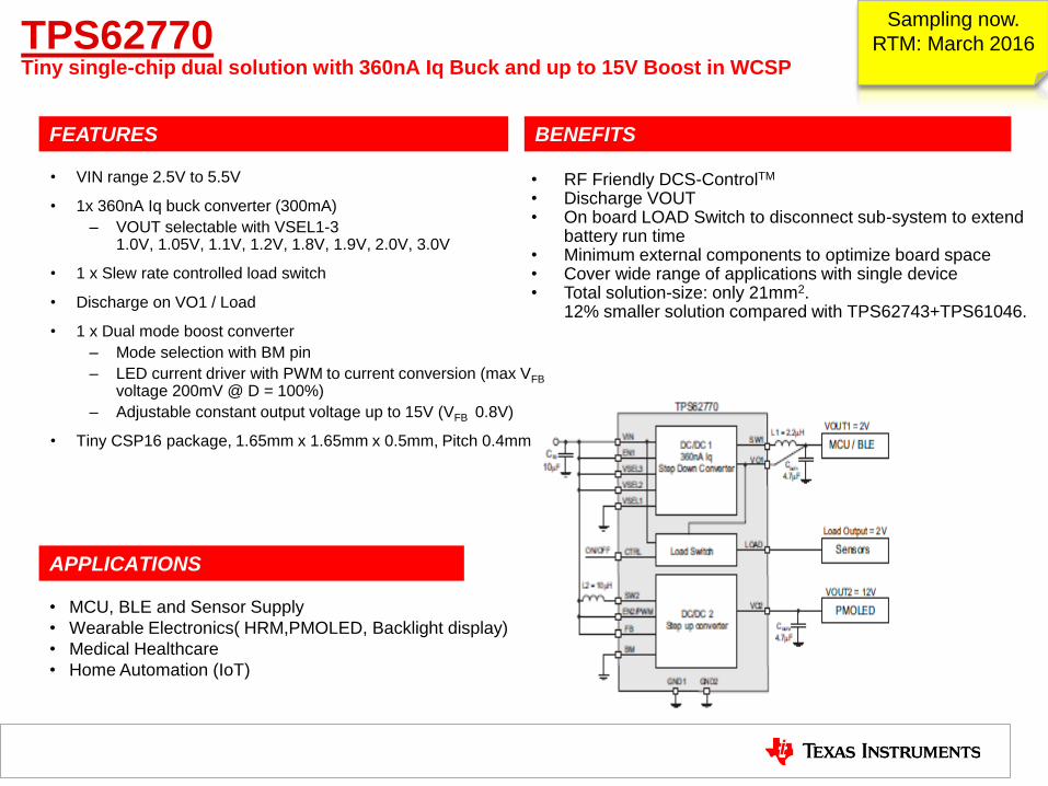
TPS62770 Tiny single-chip dual solution with 360nA Iq Buck and up to 15V Boost in WCSP
• VIN range 2.5V to 5.5V
• 1x 360nA Iq buck converter (300mA)
– VOUT selectable with VSEL1-3 1.0V, 1.05V, 1.1V, 1.2V, 1.8V, 1.9V, 2.0V, 3.0V
• 1 x Slew rate controlled load switch
• Discharge on VO1 / Load
• 1 x Dual mode boost converter
– Mode selection with BM pin
– LED current driver with PWM to current conversion (max VFB voltage 200mV @ D = 100%)
– Adjustable constant output voltage up to 15V (VFB 0.8V)
• Tiny CSP16 package, 1.65mm x 1.65mm x 0.5mm, Pitch 0.4mm
• RF Friendly DCS-ControlTM
• Discharge VOUT • On board LOAD Switch to disconnect sub-system to extend
battery run time • Minimum external components to optimize board space • Cover wide range of applications with single device • Total solution-size: only 21mm2.
12% smaller solution compared with TPS62743+TPS61046.
FEATURES BENEFITS
APPLICATIONS
• MCU, BLE and Sensor Supply
• Wearable Electronics( HRM,PMOLED, Backlight display)
• Medical Healthcare
• Home Automation (IoT)
Sampling now.
RTM: March 2016
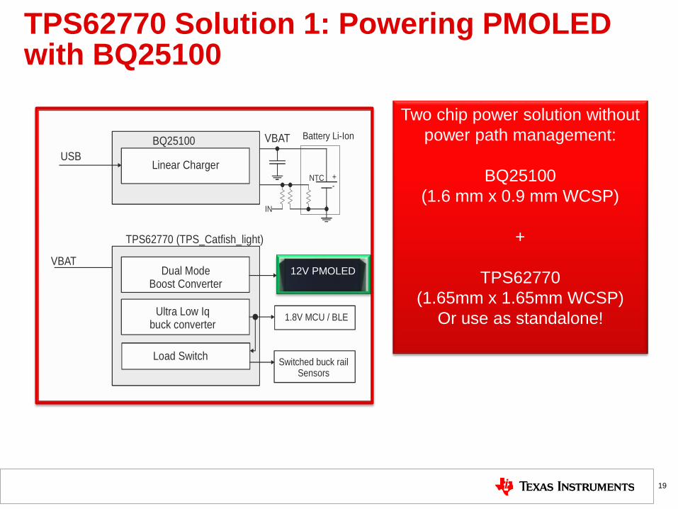
Linear Charger
BQ25100
Dual ModeBoost Converter
Ultra Low Iq buck converter
TPS62770 (TPS_Catfish_light)
12V PMOLED
Switched buck rail Sensors
Load Switch
1.8V MCU / BLE
USB
VBAT
NTC +-
Battery Li-Ion
IN
VBAT
TPS62770 Solution 1: Powering PMOLED with BQ25100
19
Two chip power solution without
power path management:
BQ25100
(1.6 mm x 0.9 mm WCSP)
+
TPS62770
(1.65mm x 1.65mm WCSP)
Or use as standalone!
12V PMOLED

TPS62770 Solution 2: Driving LED in Series for Backlight Display
20
D= 1% to 100%

TPS62770 Solution 3: Driving Green LED for HRM
21
SW2
VIN
EN2/PWMVO2
L2 = 10 H
COUT2
4.7 F
C10
IN
F
TPS62770
GND1
DC/DC 2 Step up converter
EN1
SW1
VO1
L1 = 2.2 H
C
4.7 FOUT1
VOUT1 = 2V
DC/DC 1360nA Iq
Step Down Converter
CTRLLOAD
Load Output = 2V
Load Switch
GND2
VSEL1
VSEL2
VSEL3
BM
ON/OFF
MCU / BLE
Sensors
FB
VOUT2 = 12V
PMOLED
Vout = 5V
HRM