S cientific Autonomy in Germany: The German Research Foundation

DAAAM INTERNATIONAL SCIENTIFIC BOOK 2014 pp. 239-256 Chapter 20
DEVELOPMENT OF MICRO-PLASMA WIRE
DEPOSITION PROCESS FOR LAYERED
MANUFACTURING
JHAVAR, S. & JAIN, N.K.
Abstract: This chapter presents the use of micro-plasma wire depsotion process as an alternative to the existing layer manufacturing procesess for small sized deposition. Experiments at two stages were conducted to identify important process parameters generating regular and smooth track geometry in single and multi-layer
deposition. Further investigations were conducted for enhancing the deposition quality of the process by approximating and validating the deposition. The process was found to be capable of fabricating straight walls having total wall width of 2.45 mm and effective wall width of 2.11 mm. The deposition efficiency was found to be 87% for the maximum deposition rate of 42 g/h. The microscopic examination and micro-hardness measurements revealed that the deposited wall is free from cracks, porosity and inclusions. This study confirms the capability of micro-plasma wire
depsotion process as an alternative to various established layer manufacturing processes used for meso-scale fabrication. Key words: layer manufacturing, plasma deposition, characterization, deposition
rate, tool steel
Authors´ data: Jhavar, S[uyog]; Jain, N[eelesh] K[umar], Discipline of Mechanical
Engineering, Indian Institute of Technology Indore, 453446, MP, India,
[email protected], [email protected]
This Publication has to be referred as: Jhavar, S[uyog] & Jain, N[eelesh] (2014).
Development of Micro-Plasma Wire Deposition Process for Layered Manufacturing,
Chapter 20 in DAAAM International Scientific Book 2014, pp.239-256, B. Katalinic
(Ed.), Published by DAAAM International, ISBN 978-3-901509-98-8, ISSN 1726-
9687, Vienna, Austria
DOI: 10.2507/daaam.scibook.2014.20

Jhavar, S. & Jain, N.: Development of Micro-Plasma Wire Deposition Process for L...
1. Introduction
Layer manufacturing (LM) is an advance forming process in which material is
deposited layer by layer and then two consecutive deposited layers are joined
together either to (i) produce new net-shaped or near net-shaped components; or (ii)
to add delicate features to the existing components. Fig. 1 shows the elements of a
typical LM system. Each deposited layer is created by rapid solidification of the
deposition material over a stationary or moving substrate. The Process eliminates
many steps required in the conventional manufacturing such as preparation of
drawings at different manufacturing stages, procurement of raw material of specific
shape and size, planning of man power, machines and manufacturing processes,
intermittent quality checks and allied human errors. LM technology is
interdisciplinary in nature utilizing the knowledge of computer aided
design/manufacturing (CAD/CAM), robotics, joining, sensing, monitoring, control,
etc.
Fig. 1. Elements of a typical layered manufacturing system
Diversified industries are now using LM for various rapid prototyping (RP),
rapid manufacturing (RM) and rapid tooling (RT) applications. These include
avionics and aerospace industries, automotive, biomedical, nuclear, electronics, tool-
making, special-purpose engineering, repair/remanufacturing and lifestyle Campbell
et al (2007). LM processes are used to make components for digital cameras, mobile
phones and machine parts as well as interior elements for automobiles, components
and modules for aircraft, medical and dental implants and many more. Since 1990
onwards, many LM processes have been developed, patented and commercialized
mostly for the non-metallic parts used in the various applications. However,
development of LM process for the metallic parts is still challenging and needs lot of
research to mature it.
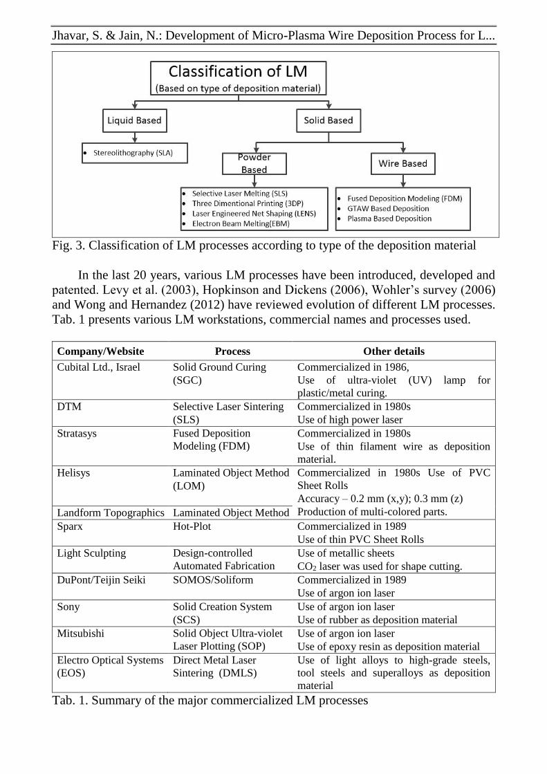
2. Classification of LM processes
Levy et al (2003) reviewed various LM processes (both patented as well as
commercialized) used for deposition of metallic materials in various RM and RT
applications. Jhavar et al (2013) presented a brief review of various LM processes as

DAAAM INTERNATIONAL SCIENTIFIC BOOK 2014 pp. 239-256 Chapter 20
repairing options for dies and moulds. Laser rapid manufacturing (LRM), laser
engineered net shaping (LENS), direct metal deposition (DMD), electron beam
melting (EBM), solid freeform fabrication (SFF), three-dimensional welding (3DW)
are some of the frequently published variants under LM technology. Various LM
processes can be classified either according to the (i) type of heat source used for
melting the material: high-energy beam processes using laser or electron beam and
electric-arc based processes; (ii) type of deposition material being used: liquid or
solid-based. Laser, electron beam and electric arc are the major energy sources used
for the LM processes for the metallic materials. Laser and electron beam are more
precise energy sources than the electric arc therefore they are more preferred for
miniature sized deposition. But, a major drawback is their poor energy conversion
efficiency which causes higher energy consumption for fabrication of components,
tooling and related applications. Use of energy efficient sources and increase in the
deposition rates are the two major concerns for LM processes. Fig. 2 presents
classification of LM processes according to the type of energy source used.
Fig. 2. Classification of the LM processes according to type of energy source
The deposition material can be supplied in the form of either liquid or solid (i.e.
powder, wire, pallets, foil, etc.) or both. Fig. 3 presents the classification of the LM
processes according to type of the deposition material. Liquid-based LM systems
were used during the initial development phase of the RP processes. These systems
utilize low melting point deposition material such as wax, polyethylene, silicon
rubber, epoxy, ABS etc. for making the prototypes. With the technological
advancement, innovative methods of using LM for manufacturing the metallic
components and tooling were developed which led to increased use of solid
deposition materials in the form of powder and/or wire. Recently developed
technological equipment have capabilities to analyse and explore various aspects of
using the deposition material in the form of powder/wire of metals, alloys, ceramics
and functionally graded materials for the LM processes.
Jhavar, S. & Jain, N.: Development of Micro-Plasma Wire Deposition Process for L...
Fig. 3. Classification of LM processes according to type of the deposition material
In the last 20 years, various LM processes have been introduced, developed and
patented. Levy et al. (2003), Hopkinson and Dickens (2006), Wohler’s survey (2006)
and Wong and Hernandez (2012) have reviewed evolution of different LM processes.
Tab. 1 presents various LM workstations, commercial names and processes used.
Company/Website Process Other details
Cubital Ltd., Israel Solid Ground Curing
(SGC)
Commercialized in 1986,
Use of ultra-violet (UV) lamp for
plastic/metal curing.
DTM
Selective Laser Sintering
(SLS)
Commercialized in 1980s
Use of high power laser
Stratasys
Fused Deposition
Modeling (FDM)
Commercialized in 1980s
Use of thin filament wire as deposition
material.
Helisys
Laminated Object Method
(LOM)
Commercialized in 1980s Use of PVC
Sheet Rolls
Accuracy – 0.2 mm (x,y); 0.3 mm (z)
Production of multi-colored parts. Landform Topographics Laminated Object Method
Sparx
Hot-Plot Commercialized in 1989
Use of thin PVC Sheet Rolls
Light Sculpting Design-controlled
Automated Fabrication
Use of metallic sheets
CO2 laser was used for shape cutting.
DuPont/Teijin Seiki SOMOS/Soliform Commercialized in 1989
Use of argon ion laser
Sony Solid Creation System
(SCS)
Use of argon ion laser
Use of rubber as deposition material
Mitsubishi Solid Object Ultra-violet
Laser Plotting (SOP)
Use of argon ion laser
Use of epoxy resin as deposition material
Electro Optical Systems
(EOS)
Direct Metal Laser
Sintering (DMLS)
Use of light alloys to high-grade steels,
tool steels and superalloys as deposition
material
Tab. 1. Summary of the major commercialized LM processes

DAAAM INTERNATIONAL SCIENTIFIC BOOK 2014 pp. 239-256 Chapter 20
3. Review of the past work
The transition of LM application from polymeric to metallic material has been
gradual and challenging. With the availability of several patents and commercial
workstations for LM of polymer based materials, the technology has matured enough,
but however same is not true for metallic materials. Laser and electron beam are more
preferred for miniature sized deposition as they are more precise energy sources than
the electric arc. But, a major drawback is their poor energy conversion efficiency
which causes higher energy consumption for fabricating the components, tooling and
related applications. Suryakumar et al. (2011) have mentioned that the deposition rate
achieved by laser or electron beam is of the order of 2-10 g/min. whereas, electric arc
based deposition processes can achieve it in the range of 50-130 g/min. Therefore, arc
based deposition techniques are preferred for bulk deposition on the metallic
components for various LM purposes. Use of energy efficient sources and increase in
the deposition rates for LM processes are two major issues. Jandric et al. (2004)
successfully built three dimensional metallic parts using gas tungsten arc welding
(GTAW) process for depositing the material. They reported that the manufactured
part was free from cracks, porosity and had uniform microstructure throughout.
Akula and Karunakaran (2006) have developed a direct metal rapid tool making
process integrating metal inert gas (MIG) and metal active gas welding (MAG) for
near-net layer deposition and computer numerical controlled (CNC) milling process
for net shaping to manufacture the dies and moulds for the metallic parts. Micro-arc
based deposition is one of the recent LM techniques having prospective applications
in repairs and fabrication at meso-scale. Horii et al. (2009) reported success in
making three dimensional structures using micro-sized wire for miniature deposition
through a micro-tungsten inert gas (μ-TIG) welding system. They mentioned that this
can be useful for meso-scale net-shaping. Almeida and Williams (2010) developed
out-of-chamber LM using gas metal arc welding (GMAW) to deposit a wall of Ti-
6Al-4V. They statistically modelled the process to predict the most appropriate
processing parameters. Baufeld et al. (2011) deposited multi-layered single bead wall
using a combination of laser beam deposition and GTAW with the help of a 6-axis
robotic system. Their results confirm that both laser and GTAW processes can be
used for LM applications. Martina et al. (2012) used plasma wire deposition to make
walls of Ti-6Al-4V. They designed their experiments using D-optimal design method
and achieved 1.8 kg/h as the highest deposition rate feeding 1.2 mm diameter wire at
100 mm/s.
Therefore, it can be understood that there is a wide gap that exists between the
process capabilities of arc-based and high-energy based depositions processes. High-
energy beam based processes are too costly for LM applications requiring miniature
or small amount of metallic deposition. No work has been reported on the
development of micro-version of arc-based processes which is economical, material-
efficient and energy-efficient.

Jhavar, S. & Jain, N.: Development of Micro-Plasma Wire Deposition Process for L...
4. Research objectives
The present research work was undertaken with the following research
objectives so as to bridge the identified research gaps:
1) To develop micro-plasma wire deposition process for LM applications for the
metallic materials so as to
Bridge the gap between the process capabilities of arc-based and high-energy
based depositions processes.
An energy-efficient, material-efficient and environment friendly alternative to
the existing LM processes.
2) To identify the ranges of process parameters for μ-plasma wire deposition process
for regular deposition.
3) To investigate the surface integrity of the deposited material in order to confirm
the process capability for LM applications.
4) To evaluate energy input per unit travel speed of worktable, volumetric feed rate
of wire per unit travel speed of worktable and material deposition rate for regular
deposition.
5) To identify the process parameters with the lowest energy input per unit travel
speed of worktable and highest deposition rate for multi-layer deposition of
straight walls.
5. Design and development of the experiment apparatus
In the present work, a computer controlled micro-plasma power supply along
with its torch was used as the power source and deposition system for the
development of the experimental apparatus for micro plasma wire deposition process.
This system had maximum plasma power capacity of 450 W with current varying in
the range of 0.1-18 A with a step of 0.1 A. A wire feeding system was designed and
developed to ensure an uninterrupted supply of the deposition material. The spool of
AISI P20 wire was loaded on the wire-feeding system which can feed the wire at rate
of 850, 1275 and 1700 mm/min. The nozzle of micro-plasma welding system was
suitably modified for feeding the wire to the melt-pool. A conventional milling
machine was used as the manipulator system to provide the required movements in
the X and Y directions. The manipulator system had capacity to provide variable
travel speed of 40, 50, 63, 80, 100 mm/min in the automatic mode with a positional
accuracy of 0.005 mm. Fig. 4 depicts the schematic diagram of the developed
experimental apparatus for the micro plasma wire deposition process for the metallic
materials.
In order to achieve the research objectives, the experiments were planned and
conducted in three stages: (i) pilot experiments for single-track deposition varying the
selected process parameters in the entire ranges available on the machine; (ii) forty
five main experiments with three replicates for single-track deposition using full

DAAAM INTERNATIONAL SCIENTIFIC BOOK 2014 pp. 239-256 Chapter 20
Fig. 4. Schematic diagram of the experimental apparatus developed for the micro
plasma wire deposition process
factorial approach; (iii) two experiments for multi-layer deposition with three
replicates. Pilot experiments helped to identify the proper ranges/values of the most
influencing parameters of micro plasma wire deposition process. Seven parameters
were selected to vary during the pilot experiments on the basis of their influence on
the performance of the micro plasma wire deposition process. They were plasma
power (P), travel speed of the worktable (v), wire feed rate (f), wire feed angle (α),
stand-off distance (X), plasma gas flow rate (Fp) and shield gas flow rate (Fs). These
parameters were varied in their entire range available on the developed experimental
apparatus as mentioned in the Tab. 2. Based upon observations during the pilot
experiments, plasma power, travel speed of the worktable and wire feed rate were
found to be the most significant parameters affecting the quality of single-track
deposition by the micro plasma wire deposition process. The ranges for these three
parameters were narrowed down while optimum values of the other four parameters
were identified for the main experiments focused on single-track deposition.
Designation: parameter name (unit) Range used for the
pilot experiments
Range / value identified for
the main experiments
P: Plasma power (W) 50 - 450 350-450
v: Travel speed of worktable
(mm/min.)
40 - 160 40-100
f: Wire feed rate (mm/min.) 850 - 1700 850-1700
α: Wire feed angle (degrees) 20 - 60 45 ± 1°
X: Stand-off distance (mm) 5 - 8 5
Fp: Plasma gas flow rate (l/min.) 0.1 - 0.5 0.4
Fs: Shield gas flow rate (l/min.) 3.0 - 8.0 5.0
Tab. 2. Input parameters and their ranges used in the pilot experiments

Jhavar, S. & Jain, N.: Development of Micro-Plasma Wire Deposition Process for L...
6. Result and discussion
It was observed during the pilot experiments that a minimum 300 W of plasma
power was required to melt the stationary AISI P20 wire of 300 µm. Further, a small portion of power is required to melt the substrate during micro plasma wire deposition process called wetting. This is required to build a strong bond between the consecutive layers. The micro-plasma power source used in the experimental apparatus had capacity to provide maximum power of 450 W. Therefore, plasma power (P) was bracketed between 350-450 W for the main experiments. Discontinuous tracks were observed when travel speed of the worktable was more than 100 mm/min, even at the maximum allowable wire feed rate of 1700 mm/min. Therefore, a range of 40-100 mm/min was selected for travel speed of the worktable. Here, the value of travel speed of worktable is limited due to available gearing ratio of the conventional milling machine, which is used as manipulator system in the developed experimental apparatus. All the designed values of wire feed rate were used in the pilot experiments. It was also experimentally found that the wire feed angle of 45 degree could produce good quality deposition at lower plasma power. This is in agreement with the previous work by (Abioye et al., 2013). Stand-off distance (SOD) of 5 mm was found to be optimum. The lower values of the SOD produces difficulty in smooth wire feeding due to smaller space, while the higher values of SOD resulted in lower plasma power density compelling higher plasma power for deposition, which results in larger HAZ. The similar results were observed by Wang et al. (2003).
Plasma gas flow rate of 0.4 litre per minute (l/min.) was found to be adequate to transfer plasma power towards the substrate, while shield gas flow rate of 5 l/min was found to be just sufficient to protect the melt pool from oxidation. It was observed that lower values of the shield gas flow rate allowed the atmospheric gases to react with the melt pool resulting in irregular (i.e., porous and uneven) deposition and spatter during deposition, whereas higher values resulted in wider melt pool generating dimple like impressions over the top surface of the deposition.
Here, the objective of the main experiments was to identify the optimum values of plasma power, wire feed rate and travel speed of the worktable based upon quality of the single-track deposition using AISI P20 wire on the substrate of the same material. Tab. 3 presents the values of the input process parameters and the average values of geometric parameters of single-track depositions in terms of geometrical aspects like deposition width, deposition height, aspect ratio, dilution, and track root angle along with their standard deviation for the 45 main experiments (Jhavar et al 2014a). It also mentions the quality of the deposition in terms of non-uniform (NU) and uniform & regular (UR). It was observed that the use of higher plasma power and lower wire feed rate caused excess melting of the substrate and deposition material and even evaporation of the deposition material causing discontinuity in the deposition and formation of the cavities which led to either no or very little deposition. While, use of lower plasma power and higher wire feed rate resulted in deposition having lower bonding between the substrate and the deposition material due to insufficient melting of the deposition material. It also resulted in collision of wire with the substrate in the extreme cases resulting in deflection of the deposition material delivery and offsetting the centre of wire from the centre of melt pool. This

DAAAM INTERNATIONAL SCIENTIFIC BOOK 2014 pp. 239-256 Chapter 20
centre offsetting caused irregular depositions due to wrong wire positioning. Hence, wire positioning is critical for better utilization of plasma energy and sound deposition. It was also noted that there is a balance of plasma power and wire feed rate required for the regular and sound deposition.
Trac
k ID
Plasma
Power
(W)
Travel speed
of worktable
(mm/min)
Wire Feed
Rate
(mm/min)
Deposition
width (mm)
Deposition
height
(mm)
Aspect
Ratio
Dilution
(%)
Track
Root
Angle
Observ
ations
1 350 40 1700 1.9± 0.1 1.8 ± 0.08 1.06 ± 0.069 1.01 ± 0.04 130 NU
2 350 50 1700 1.8 ± 0.08 1.6 ± 0.06 1.13 ± 0.058 1.46 ± 0.05 121 NU
3 350 63 1700 1.5 ± 0.06 1.3 ± 0.05 1.15 ± 0.055 1.07 ± 0.03 119 NU
4 350 80 1700 1.4 ± 0.06 1.2 ± 0.08 1.17 ± 0.079 1.72 ± 0.04 104 NU
5 350 100 1700 1.2 ± 0.05 1.0 ± 0.04 1.20 ± 0.064 3.49 ± 0.1 102 NU
6 350 40 1275 1.6 ± 0.08 1.4 ± 0.06 1.14 ± 0.066 1.02 ± 0.02 111 NU
7 350 50 1275 1.5 ± 0.04 1.3 ± 0.06 1.15 ± 0.053 1.89 ± 0.04 111 NU
8 350 63 1275 1.4 ± 0.06 1.2 ± 0.06 1.17 ± 0.066 2.46 ± 0.06 103 NU
9 350 80 1275 1.2 ± 0.04 1.0 ± 0.04 1.20 ± 0.052 2.47 ± 0.04 106 NU
10 350 100 1275 1.1 ± 0.06 0.8 ± 0.04 1.38 ± 0.074 1.59 ± 0.06 102 NU
11 350 40 850 1.5 ± 0.06 1.2 ± 0.04 1.25 ± 0.052 1.92 ± 0.06 83 NU
12 350 50 850 1.3 ± 0.06 1.0 ± 0.04 1.30 ± 0.061 2.09 ± 0.04 76 UR
13 350 63 850 1.3 ± 0.02 0.8 ± 0.06 1.63 ± 0.077 5.47 ± 0.06 74 UR
14 350 80 850 1.4 ± 0.06 0.7 ± 0.02 2.00 ± 0.052 6.80 ± 0.08 73 UR
15 350 100 850 1.5 ± 0.08 0.6 ± 0.02 2.50 ± 0.063 13.95 ± 0.16 70 NU
16 400 40 1700 2 ± 0.08 1.6 ± 0.02 1.25 ± 0.042 3.71 ± 0.06 105 NU
17 400 50 1700 2 ± 0.1 1.4 ± 0.06 1.43 ± 0.066 4.45 ± 0.12 102 NU
18 400 63 1700 1.9 ± 0.08 1.1 ± 0.06 1.73 ± 0.069 6.99 ± 0.14 83 NU
19 400 80 1700 1.8 ± 0.08 0.9 ± 0.04 2.00 ± 0.063 7.36 ± 0.08 66 NU
20 400 100 1700 1.9 ± 0.1 0.8 ± 0.04 2.38 ± 0.073 7.74 ± 0.06 61 NU
21 400 40 1275 1.9 ± 0.08 1.4 ± 0.06 1.36 ± 0.060 1.99 ± 0.04 106 NU
22 400 50 1275 1.8 ± 0.06 1.2 ± 0.04 1.50 ± 0.047 3.37 ± 0.1 98 NU
23 400 63 1275 1.8 ± 0.08 1.0 ± 0.06 1.80 ± 0.075 5.42 ± 0.14 91 NU
24 400 80 1275 1.9 ± 0.1 0.9 ± 0.04 2.11 ± 0.069 5.75 ± 0.2 82 NU
25 400 100 1275 2 ± 0.12 0.8 ± 0.04 2.50 ± 0.078 6.62 ± 0.24 75 NU
26 400 40 850 1.8 ± 008 0.9 ± 0.04 2.00 ± 0.063 4.22 ± 0.18 79 NU
27 400 50 850 1.7 ± 0.06 0.8 ± 0.02 2.13 ± 0.043 5.17 ± 0.1 77 UR
28 400 63 850 1.6 ± 0.08 0.7 ± 0.02 2.29 ± 0.058 7.29 ± 0.12 69 UR
29 400 80 850 1.8 ± 0.08 0.6 ± 0.02 3.00 ± 0.056 8.82 ± 0.16 60 UR
30 400 100 850 1.9 ± 0.1 0.5 ± 0.04 3.80 ± 0.096 10.97 ± 0.3 39 NU
31 450 40 1700 2.1 ± 0.1 1.5 ± 0.06 1.40 ± 0.062 2.88 ± 0.12 98 NU
32 450 50 1700 2.1 ± 0.1 1.3 ± 0.04 1.62 ± 0.057 5.90 ± 0.18 87 NU
33 450 63 1700 2 ± 0.1 1.0 ± 0.04 2.00 ± 0.064 6.69 ± 0.2 76 NU
34 450 80 1700 1.9 ± 0.1 0.9 ± 0.04 2.11 ± 0.069 5.92 ± 0.12 71 NU
35 450 100 1700 2.1 ± 0.1 0.8 ± 0.04 2.63 ± 0.069 20.87 ± 0.4 64 NU
36 450 40 1275 2.2 ± 0.12 1.3 ± 0.06 1.69 ± 0.071 6.18 ± 0.36 84 NU
37 450 50 1275 2.1 ± 0.08 1.1 ± 0.04 1.91 ± 0.053 7.91 ± 0.32 80 NU
38 450 63 1275 1.9 ± 0.06 0.9 ± 0.04 2.11 ± 0.055 5.12 ± 0.12 77 UR
39 450 80 1275 1.7 ± 0.08 0.7 ± 0.02 2.43 ± 0.055 3.40 ± 0.1 74 UR
40 450 100 1275 2 ± 0.08 0.6 ± 0.02 3.33 ± 0.052 1.12 ± 0.04 61 UR
41 450 40 850 1.9 ± 0.1 0.9 ± 0.04 2.11 ± 0.069 6.47 ± 0.2 77 NU
42 450 50 850 2.1 ± 0.12 0.8 ± 0.04 2.63 ± 0.076 8.66 ± 0.28 60 NU
43 450 63 850 1.8 ± 0.08 0.6 ± 0.02 3.00 ± 0.056 6.44 ± 0.22 52 NU
44 450 80 850 2 ± 0.1 0.4 ± 0.02 5.00 ± 0.071 26.09 ± 0.6 42 NU
45 450 100 850 0.6 ± 0.06 0.1 ± 0.06 6.00 ± 0.608 -- 30 NU
Tab. 3. Values of the input parameters and geometry parameters for the main
experiments (NU- Non-uniform; UR- Uniform & regular)
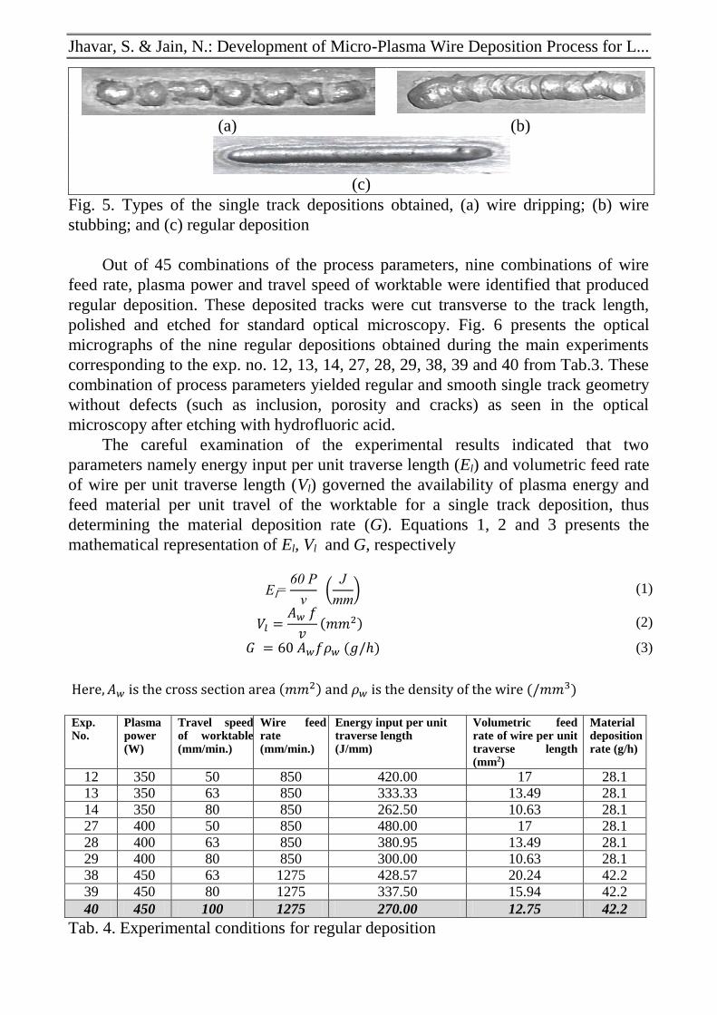
Visual examination was used to observe the quality of all 45 deposition tracks
obtained during the experiments so as to classify them in the categories of (i) wire
dripping, (ii) wire stubbing, and (ii) regular deposition, as shown in Fig. 5.
Accordingly, the corresponding parametric combinations were also identified leading
to these deposition shapes.
Jhavar, S. & Jain, N.: Development of Micro-Plasma Wire Deposition Process for L...
(a) (b)
(c)
Fig. 5. Types of the single track depositions obtained, (a) wire dripping; (b) wire
stubbing; and (c) regular deposition
Out of 45 combinations of the process parameters, nine combinations of wire
feed rate, plasma power and travel speed of worktable were identified that produced
regular deposition. These deposited tracks were cut transverse to the track length,
polished and etched for standard optical microscopy. Fig. 6 presents the optical
micrographs of the nine regular depositions obtained during the main experiments
corresponding to the exp. no. 12, 13, 14, 27, 28, 29, 38, 39 and 40 from Tab.3. These
combination of process parameters yielded regular and smooth single track geometry
without defects (such as inclusion, porosity and cracks) as seen in the optical
microscopy after etching with hydrofluoric acid.
The careful examination of the experimental results indicated that two
parameters namely energy input per unit traverse length (El) and volumetric feed rate
of wire per unit traverse length (Vl) governed the availability of plasma energy and
feed material per unit travel of the worktable for a single track deposition, thus
determining the material deposition rate (G). Equations 1, 2 and 3 presents the
mathematical representation of El, Vl and G, respectively
El=60 P
v (
J
mm) (1)
𝑉𝑙 =𝐴𝑤 𝑓
𝑣(𝑚𝑚2) (2)
𝐺 = 60 𝐴𝑤𝑓𝜌𝑤 (𝑔/ℎ) (3)
Here, 𝐴𝑤 is the cross section area (𝑚𝑚2) and 𝜌𝑤 is the density of the wire (/𝑚𝑚3)
Exp. No.
Plasma power (W)
Travel speed of worktable (mm/min.)
Wire feed rate (mm/min.)
Energy input per unit traverse length (J/mm)
Volumetric feed rate of wire per unit traverse length (mm2)
Material deposition rate (g/h)
12 350 50 850 420.00 17 28.1 13 350 63 850 333.33 13.49 28.1
14 350 80 850 262.50 10.63 28.1 27 400 50 850 480.00 17 28.1
28 400 63 850 380.95 13.49 28.1 29 400 80 850 300.00 10.63 28.1 38 450 63 1275 428.57 20.24 42.2
39 450 80 1275 337.50 15.94 42.2
40 450 100 1275 270.00 12.75 42.2
Tab. 4. Experimental conditions for regular deposition

DAAAM INTERNATIONAL SCIENTIFIC BOOK 2014 pp. 239-256 Chapter 20
Tab. 4 presents the experimental conditions for regular deposition. These
experimental conditions can be further optimized by estimation of depsotion
geometry (Jhavar et al 2014c). A comparison of various parameters as derived from
Equations 1- 3 showed that the maximum material deposition rate with least plasma
energy input per unit traverse length and nominal volume wire feed per unit traverse
length of substrate for the combination of process parameters as described for
experiment no. 40. Fig. 7 presents the process-window indicating various deposition
zones, i.e., good deposition, wire dripping and wire stubbing with respect to various
input energy per unit traverse length and wire feed per unit traverse length. It reveals
that the minimum wire feed per unit length and energy input per unit traverse length
required are 10.63 mm/min and 262.5 J/mm respectively for regular deposition.
Whereas, for regular deposition maximum wire feed per unit traverse length and
energy input per unit traverse length required are 20.24 mm/min and 480 J/mm
respectively. The data presented here is constrained by the current setup and
processing parameters. It may be noted that there was a balance of input energy per
unit traverse length and high wire feed rate required for sound deposition.
(a) (b) (c)
(d) (e) (f)
(g) (h) (i)
Fig. 6. Optical micrograph of cross-section of selected tracks (a) exp. no. 12; (b)
exp. no. 13; (c) exp. no. 14; (d) exp. no. 27; (e) exp. no. 28; (f) exp. no. 29; (g) exp.
no. 38; (h) exp. no. 39; and (i) exp. no. 40 (Jhavar et al. 2014b)

Jhavar, S. & Jain, N.: Development of Micro-Plasma Wire Deposition Process for L...
Fig. 7. Process-window indicating various deposition zones during micro-plasma
wire deposition process
Out of the nine parametric combinations, the one which gave the lowest plasma
energy input per unit traverse length and highest deposition rate (i.e. experiment no.
40 in Tab. 4) was selected for multi-layer deposition of a straight wall consisting of
15 layers with a deposition length of 50 mm for each layer. The deposition was
started from the end point of the previous layer for each subsequent layer. The
experiment was repeated thrice to confirm the process accuracy. The average values
of deposition height measured from the substrate were 7.6 mm, 8 mm and 7.8 mm for
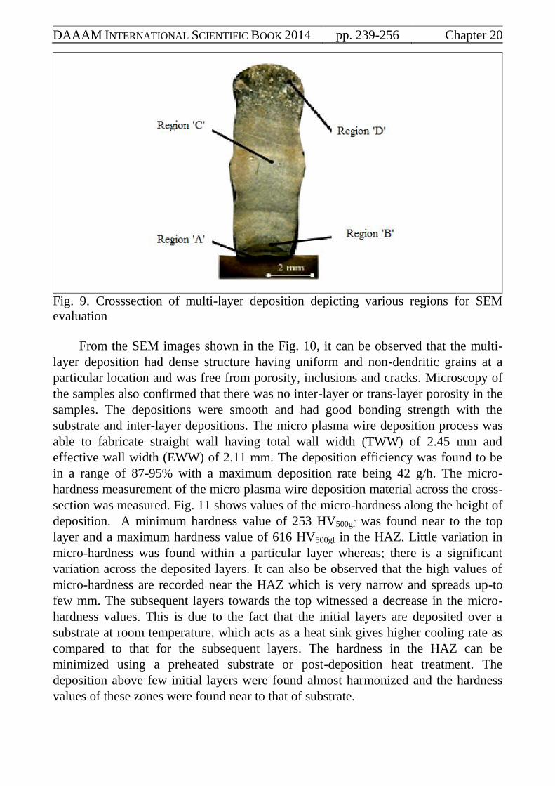
the three fabricated multi-layer deposited straight walls. Fig. 8 shows geometry of the
best quality multi-layer deposited sample. While, Fig. 9 depicts the cross-section of
multi-layer deposition. It can be seen from these figures that the multi-layer
deposition gave smooth but little wavy surface topography necessitating some
finishing operation to achieve planer deposition surface. It also signifies the complete
melting of deposition wire during deposition and good bonding between the
intermediate layers. The samples were subjected to dye penetration tests and it was
confirmed that the deposited samples were free from defects such as cracks, porosity
and inclusions at the surface.
Fig. 8. Geometry of wall fabricated by multi-layer deposition
DAAAM INTERNATIONAL SCIENTIFIC BOOK 2014 pp. 239-256 Chapter 20
Fig. 9. Crosssection of multi-layer deposition depicting various regions for SEM
evaluation
From the SEM images shown in the Fig. 10, it can be observed that the multi-
layer deposition had dense structure having uniform and non-dendritic grains at a
particular location and was free from porosity, inclusions and cracks. Microscopy of
the samples also confirmed that there was no inter-layer or trans-layer porosity in the
samples. The depositions were smooth and had good bonding strength with the
substrate and inter-layer depositions. The micro plasma wire deposition process was
able to fabricate straight wall having total wall width (TWW) of 2.45 mm and
effective wall width (EWW) of 2.11 mm. The deposition efficiency was found to be
in a range of 87-95% with a maximum deposition rate being 42 g/h. The micro-
hardness measurement of the micro plasma wire deposition material across the cross-
section was measured. Fig. 11 shows values of the micro-hardness along the height of
deposition. A minimum hardness value of 253 HV500gf was found near to the top
layer and a maximum hardness value of 616 HV500gf in the HAZ. Little variation in
micro-hardness was found within a particular layer whereas; there is a significant
variation across the deposited layers. It can also be observed that the high values of
micro-hardness are recorded near the HAZ which is very narrow and spreads up-to
few mm. The subsequent layers towards the top witnessed a decrease in the micro-
hardness values. This is due to the fact that the initial layers are deposited over a
substrate at room temperature, which acts as a heat sink gives higher cooling rate as
compared to that for the subsequent layers. The hardness in the HAZ can be
minimized using a preheated substrate or post-deposition heat treatment. The
deposition above few initial layers were found almost harmonized and the hardness
values of these zones were found near to that of substrate.

Jhavar, S. & Jain, N.: Development of Micro-Plasma Wire Deposition Process for L...
(a) (b)
(c) (d)
Fig. 10. SEM micrographs representing various parameters used to judge the
quality characteristics of multi-layer wall deposition, (a) region ‘A’ in HAZ; (b)
region ‘B’ 1mm above the substrate; (c) region ‘C’ 3 mm above the substrate and (d)
region ‘D’ 6mm above the substrate
Fig. 11. Micro-hardness profile for the best quality multi-layer deposited sample
(Jhavar et al., 2014b)

DAAAM INTERNATIONAL SCIENTIFIC BOOK 2014 pp. 239-256 Chapter 20
Fig. 12. Micro plasma wire deposition process compared with other LM processes
(Jhavar et al. 2014b)
7. Comparison of micro-plasma with Existing LM Processes
Tab. 5 presents comparison of the results of present work with some of the most recent experimental studies on multi-layer wall deposition using single bead geometry in terms of the energy source used, deposition material and its form, energy consumption per unit traverse length (J/mm), consumption rate of the deposition material, power consumption per unit deposition material consumption and TWW achieved by these processes.
Authors (year)
Type of energy source
Deposition material and its form
Energy consumption per unit traverse length (J/mm)
Consumption rate of the deposition material
Power consumption per unit deposition material consumption
TWW
Bi & Gasser (2011)
Nd:YAG laser
Powder of Ni-based super alloy
36 J/mm
1.5 g/min. 12,000 J/g 1.3 mm
Gharbi et al. (2013)
Yb:YAG laser
Powder of Ti-6Al-4V
48-75 J/mm 1 g/min. 19,200-30,000 J/g
1.9-2.1 mm
Ravi et al. (2013)
Disc laser
Powder of SC420
7.0-67.5 J/mm 2.6-12 g/min. 2,304-9,000 J/g
0.5-4.0 mm
Zhao et al. (2012)
GMAW 1.2 mm diameter wire of H08Mn2Si
1490 J/mm 2,880 mm/min. 50.4 J/mm N.A.
Present work Micro-plasma
0.3 mm diameter wire of AISI P-20 steel
270 J/mm 1,275 mm/min. 21.1 J/mm 2.45 mm
Tab. 5. Comparison of the outcome of the present work with some of the most recent experimental studies on single bead multi-layer wall deposition (Jhavar et al. 2014b) It can be observed from this comparison that though the laser based deposition processes require very less energy input per unit traverse length but their power consumption for per unit of deposition material is very high. Moreover, they have

Jhavar, S. & Jain, N.: Development of Micro-Plasma Wire Deposition Process for L...
poor energy conversion efficiency. While, conventional arc based deposition processes require very high energy per unit traverse length and use high feed rate of the deposition material but consume less power per unit deposition material consumption. They also focus higher amount of heat over larger area therefore it is difficult to use these processes for meso-scale deposition. It is evident from Table 5 that micro plasma wire deposition process is very economical and energy efficient because it requires much less power consumption per unit deposition material consumption as compared to the laser and arc based processes. Fig. 12 compares the performance of the micro plasma wire deposition process with the other competitive processes as reported by Martina et al. (2012) in terms of terms of TWW, EWW and layer height (LH). It reveals that though plasma wire deposition (PWD) can achieve smaller size deposition than the gas metal arc welding (GMAW) based processes but, it cannot achieve very small size deposition which can be achieved by the laser based processes. It is also evident from the comparison of Fig. 12 that micro plasma wire deposition process can bridge this gap and can fabricate the meso-scale components. Use of finer wire can further reduce the deposition size enabling micro plasma wire deposition process to fabricate the miniaturized parts and offer the capabilities of laser based processes at much lower cost and power consumption per unit deposition material consumption. 8. Conclusions
The work presented in this thesis illustrates the potential of micro plasma wire deposition process for layer manufacturing. Following conclusions can be drawn from the present research:
1. Micro plasma wire deposition involved low heat input as it is capable of depositing small volumes per unit length during the process.
2. For regular deposition maximum wire feed per unit traverse length and energy input per unit traverse length required are 20.24 mm/min and 480 J/mm respectively.
3. The plasma energy per unit of traverse length and volumetric wire feed rate of wire per unit traverse length were found to have threshold values of 262 J/mm and 10.6 mm3/mm respectively for the regular and continuous deposition yielding a deposition rate of 28.1 g/h.
4. The values of aspect ratio ranges between 1.3 to 4, percentage dilution ranging between 2 to 8, and track root angle ranging between 60° to 77° was observed for smooth and regular deposition.
5. Multi-layer deposition consisted of fully dense structure of good surface quality. 6. The deposition above few initial layers was found to be homogeneous and the
hardness values of these zones were found near to that of the substrate. 7. Micro-plasma wire deposition process was able to fabricate straight wall
consisting of 15 layers having TWW of 2.45 mm and a EWW of 2.11 mm with a deposition efficiency of 87%. It could achieve maximum deposition rate of 42 g/h.
8. Micro plasma wire deposition process confirmed to be cost-effective, material efficient, energy efficient and environmental friendly process for multi-layer

DAAAM INTERNATIONAL SCIENTIFIC BOOK 2014 pp. 239-256 Chapter 20
deposition and has the potential to become an alternative LM process for metallic materials.
9. Scope for the future work
The present work was the first attempt to establish micro plasma wire deposition process as an alternative to the existing LM processes therefore there is a lot of scope for future research in this area. Scope for future work may include the following:
1. Present study was conducted using conventional milling machine as manipulator system. The study can be extended to use of automated manipulators such as CNC machine or robotic arc. The deposition is expected to thereby improve in terms of deposition quality with more precision and less surface waviness.
2. Present study was limited to use of AISI P20 wires of 300μm. However, several other materials can also be used to extend the application of micro plasma wire deposition process in areas of avionics and aerospace, nuclear, biomedical and others. Use of small sized wire is also expected to give better deposition for miniaturized components.
3. Use of three dimensional heat transfer analysis using computer aided design tools (CAE) can be helpful to study the effect of plasma energy on heat affected zone and their effects can be minimized.
4. The process can be modified with the use of adaptive control to increase its capability to perfectly challenge high energy beam LM processes.
5. The process can be extended for manufacturing of functionally graded material (FGM) and metal matrix composites (MMC).
6. Use of powder based material is also an unexplored area of micro plasma wire deposition process. Its relative advantages and limitations over wire based deposition can also be studied.
10. References Abioye, T.E.; Folkes, J. & Clare, A.T. (2013). A parametric study of Inconel 625 wire laser deposition. Journal of Materials Processing Technology, 212, 203-210 Akula, S. & Karunakaran, K.P. (2006). Hybrid adaptive layer manufacturing: An Intelligent art of direct metal rapid tooling process. Robotics and Computer-Integrated Manufacturing, 22, 113-123 Almeida, P.M.S. & Williams, S. (2010). Innovative process model of Ti-6Al-4V additive layer manufacturing using cold metal transfer (CMT). Proceedings of the 21st Annual International Solid Freeform Fabrication Symposium, 25-36 Baufeld, B.; Brandl, E. & Biest, O.V.D. (2011). Wire based additive layer manufacturing: Comparison of microstructure and mechanical properties of Ti–6Al–4V components fabricated by laser-beam deposition and shaped metal deposition. Journal of Materials Processing Technology, 211, 1146-1158 Bi, G. & Gasser, A. (2011). Restoration of nickel-base turbine blade knife-edges with controlled laser aided additive manufacturing. Physics Procedia, 12, 402-209 Campbell, R.I. 2007. How designers can exploit rapid manufacturing's capabilities to add value to products. In Drstvensek, I and Katalanic, B (ed) The 1st DAAAM

Jhavar, S. & Jain, N.: Development of Micro-Plasma Wire Deposition Process for L...
International Specialized Conference on Additive Technologies, Proceedings of the 1st DAAAM International Specialized Conference on Additive, Celje, Slovenia, pp.3-4, ISBN: 3 901509 61 5 Gharbi, M.; Peyre, P., Gorny, C., Carin, M., Morville, S., Masson, P.L., Carron, D. & Fabbro, R. (2013). Influence of various process conditions on surface finishes induced by the direct metal deposition laser technique on a Ti–6Al–4V alloy. Journal of Materials Processing Technology, 213, 791- 800 Hopkinson, N. & Dickens, P., 2006. Emerging rapid manufacturing processes. In: Hopkinson, N., Hague, R., Dickens, P., (Eds.), An industrial revolution for the digital edge, John Wiley & Sons Ltd., England, pp. 55-80 Horii, T.; Kirihara, S. & Miyamoto, Y. (2009). Freeform fabrication of superalloy objects by 3D micro welding. Materials and Design, 30, 1093-1097 Jandric, Z.; Labudovic, M. & Kovacevic, R. (2004). Effect of heat sink on microstructure of three-dimensional parts built by welding-based deposition. International Journal of Machine Tools & Manufacture, 44, 785-796 Jhavar, S.; Jain, N.K. & Paul, C.P. (2014b). Development of micro-plasma transferred arc (µ-PTA) wire deposition process for additive layer manufacturing applications. Journal of Materials Processing Technology, 214, 5, 1102-1110 Jhavar, S.; Jain, N.K. & Paul, C.P. (2014c). Enhancement of deposition quality in micro-plasma transferred arc deposition process. Materials and Manufacturing Processes, 29, 8, 1017-1023 Jhavar, S.; Paul, C.P. & Jain, N.K. (2013). Causes of Failure and Repairing Options for Dies and Molds: A Review. Engineering Failure Analysis, 34, 519-535 Jhavar, S.; Paul, C.P. & Jain, N.K. (2014a). Experimental investigation on geometrical aspects of micro-plasma deposited tool steel for repair applications. International of Journal of Modern Physics: Conference Series 32, 1460347 Levy, G.N.; Schindel, R. & Kruth, J.P. (2003). Rapid manufacturing and rapid tooling with layer manufacturing (LM) technologies: state of the art and future perspectives. CIRP Annals - Manufacturing Technology, 52, 2, 589-609 Martina, F.; Mehnen, J., Williams, S.W., Colegrove, P. & Wang, F. (2012). Investigation of the benefits of plasma deposition for the additive layer manufacture of Ti–6Al–4V. Journal of Materials Processing Technology, 212, 1377-1386 Ravi, G.A.; Hao, X.J., Wain, N., Wu, X. & Attallah, M.M. (2013), Direct laser fabrication of three dimensional components using SC420 stainless steel. Materials and Design, 47, 731-736. Suryakumar, S.; Karunakaran, K.P., Bernard, A., Chandrasekhar, U., Raghavender N. & Sharma, D. (2011). Weld bead modeling and process optimization in hybrid layered manufacturing. Computer Aided Design, 43, 331-344 Wang, H.; Jiang, W., Valant, M. & Kovacevic, R. (2003). Micro plasma powder deposition as a new solid freeform fabrication process. Proceedings of the Institution of Mechanical Engineers, 217, 1641-1650 Wohlers, T. T. 2006. Rapid Prototyping & Manufacturing State of the Industry, Wohlers Report 2006. Fort Collins, CO, USA Wong, K.V. & Hernandez, A., 2012. A review of additive manufacturing. ISRN Mechanical Engineering, article ID 208760 Zhao, H.; Zhang, G., Yin, Z. & Wu, L. (2012). Three-dimensional finite element analysis of thermal stress in single-pass multi-layer weld-based rapid prototyping. Journal of Materials Processing Technology, 212, 276-285