nRF52832 NFC Antenna Tuning - Nordic Semiconductor · Revision history Date Version Description...
13
nRF52832 NFC Antenna Tuning nWP-026 White Paper v1.2 1159720_152 v1.2 / 2018-04-05
Transcript of nRF52832 NFC Antenna Tuning - Nordic Semiconductor · Revision history Date Version Description...
nRF52832 NFC AntennaTuningnWP-026
White Paperv1.2
1159720_152 v1.2 / 2018-04-05
ContentsRevision history. . . . . . . . . . . . . . . . . . . . . . . . . . . . . . . . . . iii
1 Introduction. . . . . . . . . . . . . . . . . . . . . . . . . . . . . . . . . . . 4
2 NFC antenna. . . . . . . . . . . . . . . . . . . . . . . . . . . . . . . . . . . 52.1 Choice of antenna . . . . . . . . . . . . . . . . . . . . . . . . . . . . . . . . 5
3 Estimating values. . . . . . . . . . . . . . . . . . . . . . . . . . . . . . . . 7
4 Tuning methods. . . . . . . . . . . . . . . . . . . . . . . . . . . . . . . . . 84.1 Network analyzer . . . . . . . . . . . . . . . . . . . . . . . . . . . . . . . . 84.2 Varying the frequency . . . . . . . . . . . . . . . . . . . . . . . . . . . . . . 9
4.2.1 Configuring the chip . . . . . . . . . . . . . . . . . . . . . . . . . . . . . 11
Legal notices. . . . . . . . . . . . . . . . . . . . . . . . . . . . . . . . . . . 13
1159720_152 v1.2 ii
Revision history
Date Version Description
April 2018 1.2 Update to the chip configuration process in Configuring the chip onpage 11
August 2017 1.1 Added information on overcoupling to the chapter Choice ofantenna on page 5
October 2016 1.0 First release
1159720_152 v1.2 iii
1 Introduction
This white paper describes how the nRF52832 NFC (Near Field Communication) antenna can be tuned.
A typical NFC system consists of two devices, an active and a passive device. The active device has a powersource and induces a magnetic field with a coil inductor antenna. When the passive device is placed in thismagnetic field, the varying magnetic field will induce current (power) in the passive device. The inducedpower in the passive device is used to retrieve and transmit data back to the active device.
An active device can also be called a poller, and a passive device can also be called a listener or a tag. ThenRF52832 SoC is an NFC tag device.
1159720_152 v1.2 4
2 NFC antenna
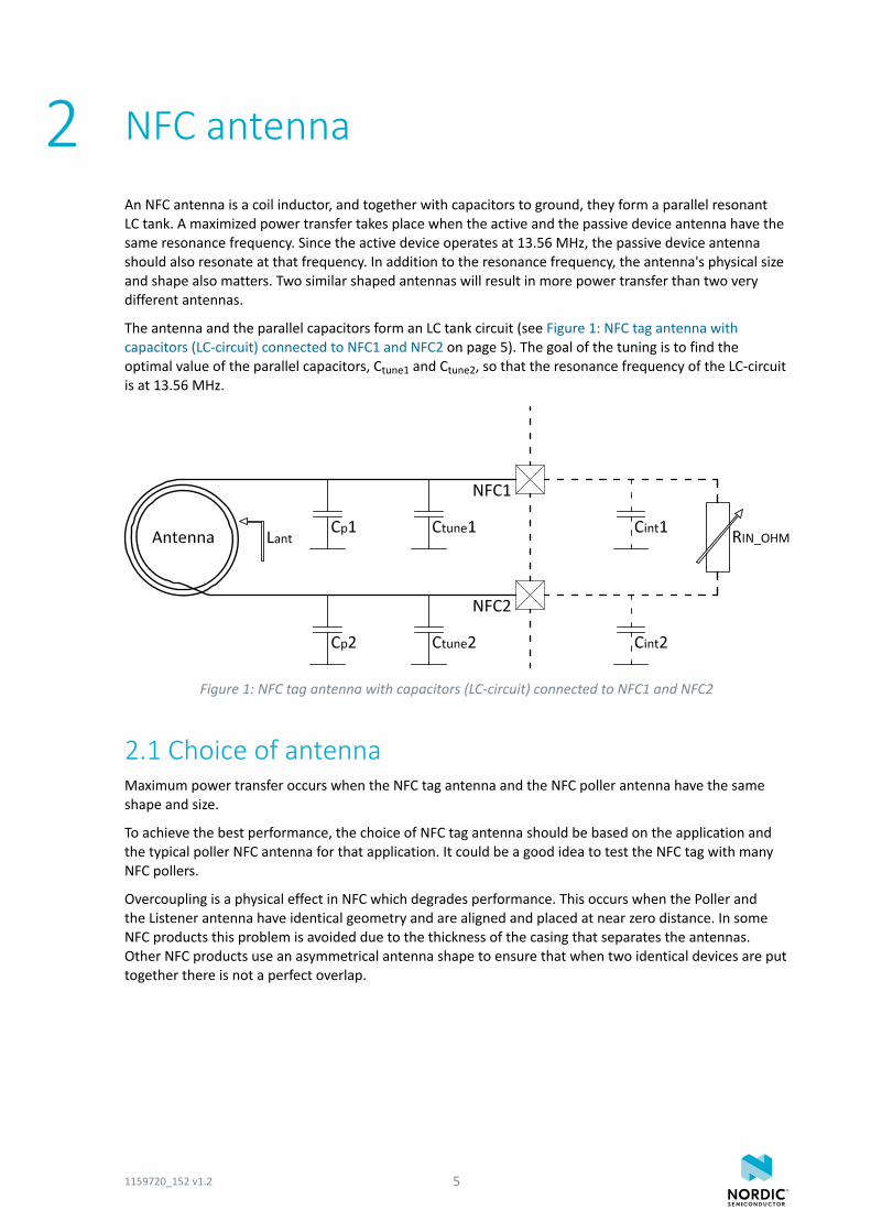
An NFC antenna is a coil inductor, and together with capacitors to ground, they form a parallel resonantLC tank. A maximized power transfer takes place when the active and the passive device antenna have thesame resonance frequency. Since the active device operates at 13.56 MHz, the passive device antennashould also resonate at that frequency. In addition to the resonance frequency, the antenna's physical sizeand shape also matters. Two similar shaped antennas will result in more power transfer than two verydifferent antennas.
The antenna and the parallel capacitors form an LC tank circuit (see Figure 1: NFC tag antenna withcapacitors (LC-circuit) connected to NFC1 and NFC2 on page 5). The goal of the tuning is to find theoptimal value of the parallel capacitors, Ctune1 and Ctune2, so that the resonance frequency of the LC-circuitis at 13.56 MHz.
Figure 1: NFC tag antenna with capacitors (LC-circuit) connected to NFC1 and NFC2
2.1 Choice of antennaMaximum power transfer occurs when the NFC tag antenna and the NFC poller antenna have the sameshape and size.
To achieve the best performance, the choice of NFC tag antenna should be based on the application andthe typical poller NFC antenna for that application. It could be a good idea to test the NFC tag with manyNFC pollers.
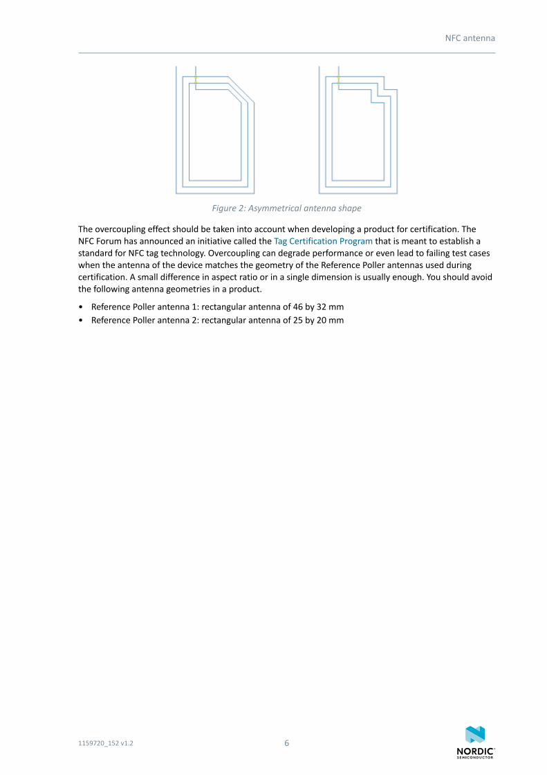
Overcoupling is a physical effect in NFC which degrades performance. This occurs when the Poller andthe Listener antenna have identical geometry and are aligned and placed at near zero distance. In someNFC products this problem is avoided due to the thickness of the casing that separates the antennas.Other NFC products use an asymmetrical antenna shape to ensure that when two identical devices are puttogether there is not a perfect overlap.
1159720_152 v1.2 5
NFC antenna
Figure 2: Asymmetrical antenna shape
The overcoupling effect should be taken into account when developing a product for certification. TheNFC Forum has announced an initiative called the Tag Certification Program that is meant to establish astandard for NFC tag technology. Overcoupling can degrade performance or even lead to failing test caseswhen the antenna of the device matches the geometry of the Reference Poller antennas used duringcertification. A small difference in aspect ratio or in a single dimension is usually enough. You should avoidthe following antenna geometries in a product.
• Reference Poller antenna 1: rectangular antenna of 46 by 32 mm• Reference Poller antenna 2: rectangular antenna of 25 by 20 mm
1159720_152 v1.2 6
3 Estimating values
Before starting to tune, you must estimate an approximate value for the capacitors Ctune1 and Ctune2.
Coming up with an estimation is important especially when using the method described in Varying thefrequency on page 9, because this method uses the estimated value to find the correct value of Ctune1and Ctune2.
Important: Ctune1 and Ctune2 must have the same value.
Complete the following steps to estimate the value of the capacitors, Ctune1 and Ctune2:
1. Find an approximate inductance (Lant) of the NFC tag antenna using an appropriate method:
• Find the value in the antenna datasheet.• Calculate the inductance based on the antenna dimensions.
2. Calculate the value of the parallel capacitors, based on the inductance of the NFC antenna.
Ctune1 and Ctune2 must have the same value, the internal capacitance Cint is approximately 4 pF, and Lantis the inductance of the NFC antenna.
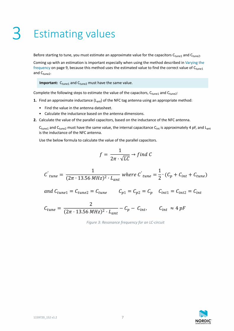
Use the below formula to calculate the value of the parallel capacitors.
Figure 3: Resonance frequency for an LC-circuit
1159720_152 v1.2 7
4 Tuning methods
There are different methods for tuning. For example, you can use a network analyzer or vary thefrequency.
Using an Network analyzer is the preferred method because there are less sources of error, and thenetwork analyzer gives actual results: For a given measurement, the network analyzer shows theresonance frequency for the tag antenna. See Network analyzer on page 8.
The method Varying the frequency uses an oscilloscope to measure the maximum voltage swing. Thismethod has more sources of errors and gives relative results. The maximum voltage swing among theresults is what is of interest, one measurement only will not give much value. See Varying the frequencyon page 9.
For the final results, it will not matter which method was used as long as the NFC tag antenna resonates at13.56 MHz after tuning.
4.1 Network analyzerThe network analyzer (S11, dB magnitude) measures the return loss in the coil antenna over a frequencyspan to find the optimal value of the parallel capacitors.
The frequency that results in a dip is the resonance frequency of the NFC tag antenna. When using thismethod, the nRF52832 chip does not need to be powered. However, if the nRF52832 SoC is powered, RINhas to be set to a fixed value. See Configuring the chip on page 11 for more details.
The required equipment for this method is:
• Network analyzer with minimum one port. The frequency range needs to cover 13.56 MHz.• Coil antenna, for example, a metal wire in a coil.• NFC tag antenna connected to the board with the nRF52832 SoC.
Complete the following steps to tune the antenna with the network analyzer method:
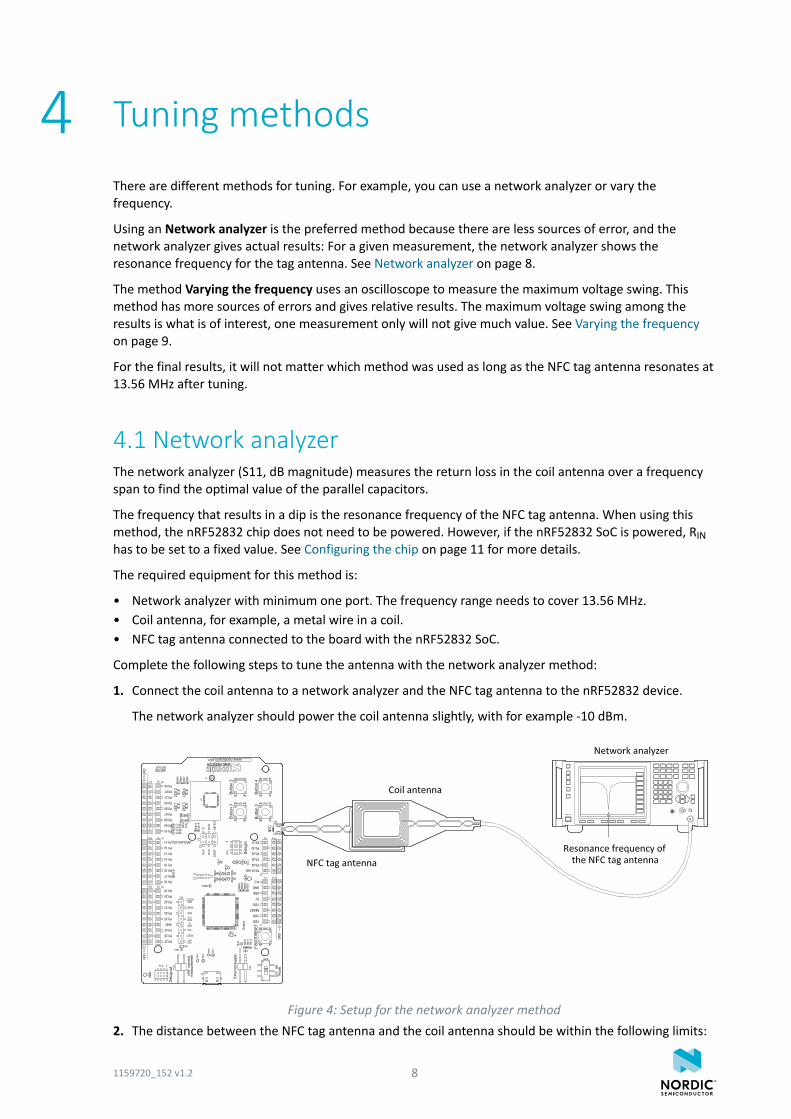
1. Connect the coil antenna to a network analyzer and the NFC tag antenna to the nRF52832 device.
The network analyzer should power the coil antenna slightly, with for example -10 dBm.
Figure 4: Setup for the network analyzer method2. The distance between the NFC tag antenna and the coil antenna should be within the following limits:
1159720_152 v1.2 8
Tuning methods
• Lower limit: A too short distance between the two antennas will pull the resonance frequencydown. The distance should therefore not be shorter than approximately 1 cm.
• Upper limit: The longer the distance between the antennas is, the weaker the loss dip in thenetwork analyzer will be. To measure the resonance frequency, the loss dip must be visible.
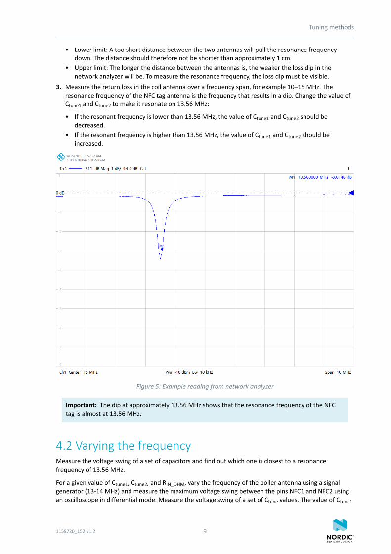
3. Measure the return loss in the coil antenna over a frequency span, for example 10–15 MHz. Theresonance frequency of the NFC tag antenna is the frequency that results in a dip. Change the value ofCtune1 and Ctune2 to make it resonate on 13.56 MHz:
• If the resonant frequency is lower than 13.56 MHz, the value of Ctune1 and Ctune2 should bedecreased.
• If the resonant frequency is higher than 13.56 MHz, the value of Ctune1 and Ctune2 should beincreased.
Figure 5: Example reading from network analyzer
Important: The dip at approximately 13.56 MHz shows that the resonance frequency of the NFCtag is almost at 13.56 MHz.
4.2 Varying the frequencyMeasure the voltage swing of a set of capacitors and find out which one is closest to a resonancefrequency of 13.56 MHz.
For a given value of Ctune1, Ctune2, and RIN_OHM, vary the frequency of the poller antenna using a signalgenerator (13-14 MHz) and measure the maximum voltage swing between the pins NFC1 and NFC2 usingan oscilloscope in differential mode. Measure the voltage swing of a set of Ctune values. The value of Ctune1
1159720_152 v1.2 9
Tuning methods
and Ctune2 that results in the highest voltage swing at 13.56 MHz, will be best value among the tested onesfor that antenna. The value of Ctune1 and Ctune2 with the highest voltage swing will be the value that resultsin an LC circuit with resonance frequency closest to 13.56 MHz, among the tested values.
The required equipment for this method is:
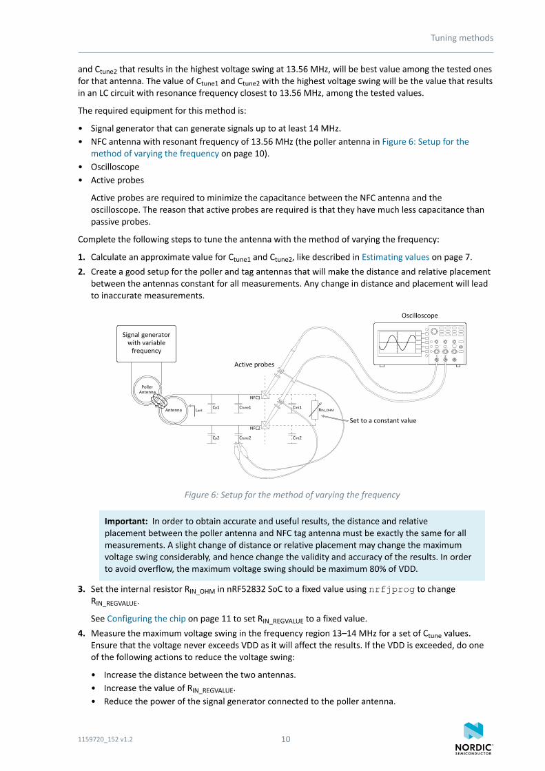
• Signal generator that can generate signals up to at least 14 MHz.• NFC antenna with resonant frequency of 13.56 MHz (the poller antenna in Figure 6: Setup for the
method of varying the frequency on page 10).• Oscilloscope• Active probes
Active probes are required to minimize the capacitance between the NFC antenna and theoscilloscope. The reason that active probes are required is that they have much less capacitance thanpassive probes.
Complete the following steps to tune the antenna with the method of varying the frequency:
1. Calculate an approximate value for Ctune1 and Ctune2, like described in Estimating values on page 7.2. Create a good setup for the poller and tag antennas that will make the distance and relative placement
between the antennas constant for all measurements. Any change in distance and placement will leadto inaccurate measurements.
Figure 6: Setup for the method of varying the frequency
Important: In order to obtain accurate and useful results, the distance and relativeplacement between the poller antenna and NFC tag antenna must be exactly the same for allmeasurements. A slight change of distance or relative placement may change the maximumvoltage swing considerably, and hence change the validity and accuracy of the results. In orderto avoid overflow, the maximum voltage swing should be maximum 80% of VDD.
3. Set the internal resistor RIN_OHM in nRF52832 SoC to a fixed value using nrfjprog to changeRIN_REGVALUE.
See Configuring the chip on page 11 to set RIN_REGVALUE to a fixed value.4. Measure the maximum voltage swing in the frequency region 13–14 MHz for a set of Ctune values.
Ensure that the voltage never exceeds VDD as it will affect the results. If the VDD is exceeded, do oneof the following actions to reduce the voltage swing:
• Increase the distance between the two antennas.• Increase the value of RIN_REGVALUE.• Reduce the power of the signal generator connected to the poller antenna.
1159720_152 v1.2 10
Tuning methods
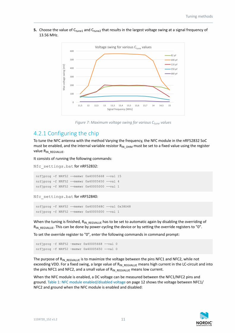
5. Choose the value of Ctune1 and Ctune2 that results in the largest voltage swing at a signal frequency of13.56 MHz.
Figure 7: Maximum voltage swing for various Ctune values
4.2.1 Configuring the chipTo tune the NFC antenna with the method Varying the frequency, the NFC module in the nRF52832 SoCmust be enabled, and the internal variable resistor RIN_OHM must be set to a fixed value using the registervalue RIN_REGVALUE.
It consists of running the following commands:
Nfc_settings.bat for nRF52832:
nrfjprog -f NRF52 --memwr 0x40005668 --val 15
nrfjprog -f NRF52 --memwr 0x40005650 --val 4
nrfjprog -f NRF52 --memwr 0x40005000 --val 1
Nfc_settings.bat for nRF52840:
nrfjprog -f NRF52 --memwr 0x4000568C --val 0x38D48
nrfjprog -f NRF52 --memwr 0x40005000 --val 1
When the tuning is finished, RIN_REGVALUE has to be set to automatic again by disabling the overriding ofRIN_REGVALUE. This can be done by power-cycling the device or by setting the override registers to "0".
To set the override register to "0", enter the following commands in command prompt:
nrfjprog –f NRF52 –memwr 0x40005668 --val 0
nrfjprog –f NRF52 –memwr 0x40005650 --val 0
The purpose of RIN_REGVALUE is to maximize the voltage between the pins NFC1 and NFC2, while notexceeding VDD. For a fixed swing, a large value of RIN_REGVALUE means high current in the LC-circuit and intothe pins NFC1 and NFC2, and a small value of RIN_REGVALUE means low current.
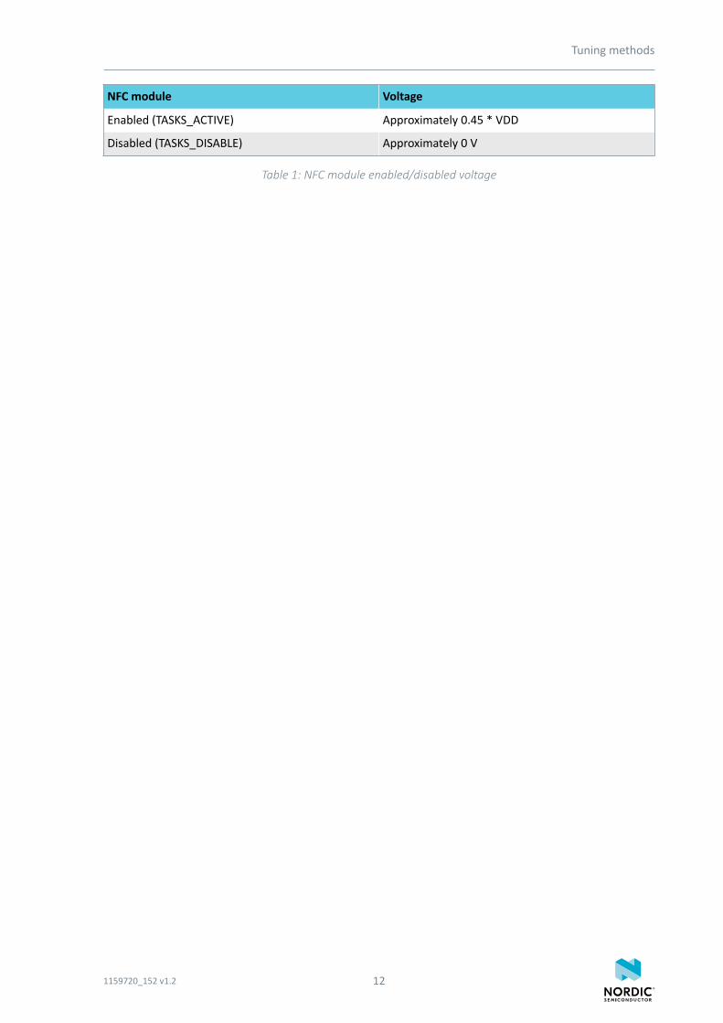
When the NFC module is enabled, a DC voltage can be measured between the NFC1/NFC2 pins andground. Table 1: NFC module enabled/disabled voltage on page 12 shows the voltage between NFC1/NFC2 and ground when the NFC module is enabled and disabled:
1159720_152 v1.2 11
Tuning methods
NFC module Voltage
Enabled (TASKS_ACTIVE) Approximately 0.45 * VDD
Disabled (TASKS_DISABLE) Approximately 0 V
Table 1: NFC module enabled/disabled voltage
1159720_152 v1.2 12
Legal noticesBy using this documentation you agree to our terms and conditions of use. Nordic Semiconductor maychange these terms and conditions at any time without notice.
Liability disclaimerNordic Semiconductor ASA reserves the right to make changes without further notice to the product toimprove reliability, function or design. Nordic Semiconductor ASA does not assume any liability arising outof the application or use of any product or circuits described herein.
All information contained in this document represents information on the product at the time ofpublication. Nordic Semiconductor ASA reserves the right to make corrections, enhancements, and otherchanges to this document without notice. While Nordic Semiconductor ASA has used reasonable carein preparing the information included in this document, it may contain technical or other inaccuracies,omissions and typographical errors. Nordic Semiconductor ASA assumes no liability whatsoever for anydamages incurred by you resulting from errors in or omissions from the information included herein.
Life support applicationsNordic Semiconductor products are not designed for use in life support appliances, devices, or systemswhere malfunction of these products can reasonably be expected to result in personal injury.
Nordic Semiconductor ASA customers using or selling these products for use in such applications do soat their own risk and agree to fully indemnify Nordic Semiconductor ASA for any damages resulting fromsuch improper use or sale.
RoHS and REACH statementNordic Semiconductor products meet the requirements of Directive 2011/65/EU of the EuropeanParliament and of the Council on the Restriction of Hazardous Substances (RoHS 2) and the requirementsof the REACH regulation (EC 1907/2006) on Registration, Evaluation, Authorization and Restriction ofChemicals.
The SVHC (Substances of Very High Concern) candidate list is continually being updated. Completehazardous substance reports, material composition reports and latest version of Nordic's REACHstatement can be found on our website www.nordicsemi.com.
TrademarksAll trademarks, service marks, trade names, product names and logos appearing in this documentation arethe property of their respective owners.
Copyright notice© 2018 Nordic Semiconductor ASA. All rights are reserved. Reproduction in whole or in part is prohibitedwithout the prior written permission of the copyright holder.
1159720_152 v1.2 13
![[nRF52832] MDBT42V-AT & MDBT42V-PAT - Version H](https://static.fdocuments.in/doc/165x107/6274638513d40b21d5452350/nrf52832-mdbt42v-at-amp-mdbt42v-pat-version-h.jpg)