Novel Transparent and Self‐Powered UV Photodetector...
9
FULL PAPER 1703754 (1 of 9) www.small-journal.com small NANO MICRO © 2018 WILEY-VCH Verlag GmbH & Co. KGaA, Weinheim Novel Transparent and Self-Powered UV Photodetector Based on Crossed ZnO Nanofiber Array Homojunction Yi Ning, Zhiming Zhang, Feng Teng, and Xiaosheng Fang* Y. Ning, Dr. Z. M. Zhang, Dr. F. Teng, Prof. X. S. Fang Department of Materials Science Fudan University Shanghai 200433, P. R. China E-mail: [email protected] The ORCID identification number(s) for the author(s) of this article can be found under https://doi.org/10.1002/smll.201703754. DOI: 10.1002/smll.201703754 D, while long-time exposure to UV radia- tion is a potential cause for skin cancer. [11] Though most short wavelength UV radia- tion can be absorbed by the stratospheric ozone, UVA radiation can easily reach the surface of people’s skin and can only be partially obstructed by sunscreen. [12] Therefore, precise detection of UVA is beneficial for related health studies, and can help researchers formulate efficient countermeasures. Zinc oxide (ZnO), as a typical wide bandgap semiconductor, has already been applied to UVA detection owing to its appropriate bandgap (≈3.37 eV) and high exciton binding energy (≈60 meV). [13] In spite of relatively low dark current and high on–off ratio reported recently, [14,15] ZnO nanowire-based UV detectors still suffer from slow response which elimi- nates their broader use in optoelectronic devices. [16] Mean- while, like many other wide bandgap semiconductors, ZnO shows intrinsic n-type conductivity due to the naturally formed internal defects, which implies the difficulty to achieve stable p-type doping. [13,17] In consequence, other p-type materials including CuSCN, [18] NiO, [19] GaN, [20] PEDOT:PSS [21] are com- monly applied to build heterojunctions with ZnO, leading to more complexity and mismatch in device structure. Though some researchers have reported the fabrication of p-type ZnO and related homojunction photodetectors by doping Cu, [22] Li, [23] Sb [24] using hydrothermal or CVD process, few have obtained stable self-powered response at zero bias and their on–off ratios are mostly around the magnitude of 10 1 at reverse bias which is much inferior to those of pure ZnO photoconductors. [14–16] Aimed at solving the abovementioned problems, we intro- duce a novel self-powered UV detector based on ZnO homo- junction using a simple doping method which is concretely described in the Experimental Section. Pure and doped ZnO nanofiber arrays are prepared via electrospinning, a low-cost and convenient fabrication method. It is reported that electro- spun polymer fibers can be used as a template to construct 1D functional devices, [25] but metallic oxides nanofibers can also be fabricated directly along with annealing. In our work, a proportional amount of Zn 2+ and Ag + (mole ratio Ag: Zn = 1:10) is directly added to the electrospinning precursor for doping. A three-electrode collector is applied to achieve highly oriented fiber arrays which shall serve as building blocks for subsequent functional devices. After precise characterization of Ag-doped ZnO nanofibers, the p-type conductivity induced by Ag + dopants is confirmed. Thus, with pure ZnO and Ag-doped A novel self-powered UV photodetector based on electrospun ZnO nanofiber arrays is introduced. Aligned pure ZnO nanofibers and Ag-doped p-type ZnO nanofibers are processed perpendicular to each other, and p–n junction arrays of ZnO nanofibers are fabricated as a result. Owing to the intrinsic inter- vals between nanofibers, the device is fully transparent on quartz substrate. Various characterization methods including TEM, XRD, and XPS are used to testify the existence form of Ag element in ZnO nanofibers, and a field effect transistor is constructed to judge their conductivity. It is discovered that the Ag doping process not only transforms ZnO to p-type conductivity, making it possible to build this self-powered photodetector, but also forms Ag nanopar- ticles in ZnO nanofibers and thus helps reduce the response time. Benefiting from the abovementioned dual effects, this UV detector is found to have an enhanced performance, with the on–off ratio up to 10 4 at zero bias and a rather short rise/decay time of 3.90 s/4.71 s. Transparent Electronics 1. Introduction In recent years, with gathered studies in low-dimensional devices, 1D nanoarrays such as nanowires, nanofibers, and nanotubes, have attracted the attention from researchers world- wide. [1–3] As for functional applications, controllable orientation and periodic arrays can work as basic building blocks for wiring, interconnecting, and functional modules in nanoelectronics and nanooptoelectronics. [1,4] Especially in the photodetecting field, the unique properties such as high surface-to-volume ratio, anisotropic transmission characteristics, [5] and great transparency, [6] have made 1D nanoarrays a prospective option for constructing photodetectors which have been playing a cru- cial role in optoelectronic circuits, [7] optical communication, [8] and video imaging. [9] Among these photodetectors, ultraviolet detectors have drawn great attention owing to people’s concerns on the UV light. UV radiation spectrum is usually divided into three bands according to the wavelength: UVC (100–280 nm), UVB (280–320 nm), and UVA (320–400 nm). [10] It is known that temperate UV light is indispensable for synthesis of Vitamin Small 2018, 14, 1703754
-
Upload
dinhkhuong -
Category
Documents
-
view
224 -
download
0
Transcript of Novel Transparent and Self‐Powered UV Photodetector...

FULL PAPER
1703754 (1 of 9)
www.small-journal.comsmall
NANO MICRO
© 2018 WILEY-VCH Verlag GmbH & Co. KGaA, Weinheim
Novel Transparent and Self-Powered UV Photodetector Based on Crossed ZnO Nanofiber Array Homojunction
Yi Ning, Zhiming Zhang, Feng Teng, and Xiaosheng Fang*
Y. Ning, Dr. Z. M. Zhang, Dr. F. Teng, Prof. X. S. FangDepartment of Materials ScienceFudan UniversityShanghai 200433, P. R. ChinaE-mail: [email protected]
The ORCID identification number(s) for the author(s) of this article can be found under https://doi.org/10.1002/smll.201703754.
DOI: 10.1002/smll.201703754
D, while long-time exposure to UV radia-tion is a potential cause for skin cancer.[11] Though most short wavelength UV radia-tion can be absorbed by the stratospheric ozone, UVA radiation can easily reach the surface of people’s skin and can only be partially obstructed by sunscreen.[12] Therefore, precise detection of UVA is beneficial for related health studies, and can help researchers formulate efficient countermeasures.
Zinc oxide (ZnO), as a typical wide bandgap semiconductor, has already been applied to UVA detection owing to its appropriate bandgap (≈3.37 eV) and high exciton binding energy (≈60 meV).[13] In spite of relatively low dark current and high on–off ratio reported recently,[14,15] ZnO nanowire-based UV detectors still suffer from slow response which elimi-
nates their broader use in optoelectronic devices.[16] Mean-while, like many other wide bandgap semiconductors, ZnO shows intrinsic n-type conductivity due to the naturally formed internal defects, which implies the difficulty to achieve stable p-type doping.[13,17] In consequence, other p-type materials including CuSCN,[18] NiO,[19] GaN,[20] PEDOT:PSS[21] are com-monly applied to build heterojunctions with ZnO, leading to more complexity and mismatch in device structure. Though some researchers have reported the fabrication of p-type ZnO and related homojunction photodetectors by doping Cu,[22] Li,[23] Sb[24] using hydrothermal or CVD process, few have obtained stable self-powered response at zero bias and their on–off ratios are mostly around the magnitude of 101 at reverse bias which is much inferior to those of pure ZnO photoconductors.[14–16]
Aimed at solving the abovementioned problems, we intro-duce a novel self-powered UV detector based on ZnO homo-junction using a simple doping method which is concretely described in the Experimental Section. Pure and doped ZnO nanofiber arrays are prepared via electrospinning, a low-cost and convenient fabrication method. It is reported that electro-spun polymer fibers can be used as a template to construct 1D functional devices,[25] but metallic oxides nanofibers can also be fabricated directly along with annealing. In our work, a proportional amount of Zn2+ and Ag+ (mole ratio Ag: Zn = 1:10) is directly added to the electrospinning precursor for doping. A three-electrode collector is applied to achieve highly oriented fiber arrays which shall serve as building blocks for subsequent functional devices. After precise characterization of Ag-doped ZnO nanofibers, the p-type conductivity induced by Ag+ dopants is confirmed. Thus, with pure ZnO and Ag-doped
A novel self-powered UV photodetector based on electrospun ZnO nanofiber arrays is introduced. Aligned pure ZnO nanofibers and Ag-doped p-type ZnO nanofibers are processed perpendicular to each other, and p–n junction arrays of ZnO nanofibers are fabricated as a result. Owing to the intrinsic inter-vals between nanofibers, the device is fully transparent on quartz substrate. Various characterization methods including TEM, XRD, and XPS are used to testify the existence form of Ag element in ZnO nanofibers, and a field effect transistor is constructed to judge their conductivity. It is discovered that the Ag doping process not only transforms ZnO to p-type conductivity, making it possible to build this self-powered photodetector, but also forms Ag nanopar-ticles in ZnO nanofibers and thus helps reduce the response time. Benefiting from the abovementioned dual effects, this UV detector is found to have an enhanced performance, with the on–off ratio up to 104 at zero bias and a rather short rise/decay time of 3.90 s/4.71 s.
Transparent Electronics
1. Introduction
In recent years, with gathered studies in low-dimensional devices, 1D nanoarrays such as nanowires, nanofibers, and nanotubes, have attracted the attention from researchers world-wide.[1–3] As for functional applications, controllable orientation and periodic arrays can work as basic building blocks for wiring, interconnecting, and functional modules in nanoelectronics and nanooptoelectronics.[1,4] Especially in the photodetecting field, the unique properties such as high surface-to-volume ratio, anisotropic transmission characteristics,[5] and great transparency,[6] have made 1D nanoarrays a prospective option for constructing photodetectors which have been playing a cru-cial role in optoelectronic circuits,[7] optical communication,[8] and video imaging.[9] Among these photodetectors, ultraviolet detectors have drawn great attention owing to people’s concerns on the UV light. UV radiation spectrum is usually divided into three bands according to the wavelength: UVC (100–280 nm), UVB (280–320 nm), and UVA (320–400 nm).[10] It is known that temperate UV light is indispensable for synthesis of Vitamin
Small 2018, 14, 1703754

1703754 (2 of 9)
www.advancedsciencenews.com www.small-journal.comsmall
NANO MICRO
© 2018 WILEY-VCH Verlag GmbH & Co. KGaA, Weinheim
ZnO nanofibers simply connected to form p–n junction, the obtained UV photodetector exhibits high-performance self-powered photoresponse, reaching a perfect balance between sensitivity and response time under zero voltage bias. This device also shows great transparency of averagely 89% at visible range and 84% at UV range on quartz substrate.
2. Results and Discussion
Figure 1a,b shows the transmission electron microscopy (TEM) image of as-prepared pure ZnO nanofiber and Ag-doped ZnO nanofiber. The electrospun nanofibers are made of stacked crys-talline grains and the width is around 500 nm as depicted. Espe-cially in Figure 1b, a dark metal nanoparticle is precipitated in the Ag-doped ZnO nanofiber with the diameter of about 250 nm. In the annealing process after electrospinning, extra Ag atoms aggregate to form nanoparticles inside the nanofibers. To con-firm the nanofibers’ composition, the lattice structure of certain grain can be observed directly from the high-resolution trans-mission electron microscopy (HRTEM) images in Figure 1c,d, with the spacing of 2.60, 2.81, 2.47, and 2.37 Å. According to
cards PDF#65-3411 and PDF#01-1164, these data correspond to ZnO (002), (100), (101), and Ag (111), respectively, suggesting that both wurtzite ZnO and metal Ag exist.
The crystal structures of prepared nanofibers are further ana-lyzed through X-ray diffraction (XRD). The full spectra of Ag-doped ZnO and pure ZnO in Figure 2a agree with the above-mentioned measurements of spacing d. More interestingly, fine analysis toward diffraction peaks ranging from 31° to 37° in Figure 2b shows a small shift (≈0.16°) to a lower 2θ angle for Ag-doped ZnO, as compared to those of pure ZnO. The spacing d can be calculated according to Bragg’s law
2 sind nθ λ= (1)
where n is the order of diffraction (usually n = 1) and λ is the X-ray wavelength (Cu Kα, λ = 1.5405 Å). For wurtzite ZnO, the lattice constants are calculated by
2
3d , 2d100 002a c= =( ) ( )
(2)
Herein, the lattice constants a and c are calculated as a = 3.249 Å and c = 5.207 Å for pure ZnO. An increase for lattice constants a and c to 3.265 and 5.229 Å occurs in Ag-doped ZnO
Small 2018, 14, 1703754
Figure 1. a) TEM image of pure ZnO nanofiber. b) TEM image of Ag-doped ZnO nanofiber. c) HRTEM image of pure ZnO nanofiber. d) HRTEM image of Ag-doped ZnO nanofiber.

1703754 (3 of 9)
www.advancedsciencenews.com www.small-journal.comsmall
NANO MICRO
© 2018 WILEY-VCH Verlag GmbH & Co. KGaA, Weinheim
simultaneously. From the reduced diffraction angle, the spac-ings of plane (100), (101), (002) have all increased in Ag-doped ZnO and its lattice has expanded. It is known that the radius of Ag+ (1.26 Å) is larger than that of Zn2+ (0.74 Å). This result indicates that not only do Ag atoms exist in the precipitated nanoparticles, but some Ag+ ions also exist in the ZnO crystals, substituting some Zn2+ ions, finally leading to distortion of the ZnO lattice.[26,27]
To determine the exact chemical state of certain ele-ments in the Ag-doped nanofibers, X-ray photoelectron spec-troscopy (XPS) is performed and the results are shown in Figure 2c. Certain atoms in different chemical environments show minute differences in their binding energies and their specific bonding with other atoms can be clarified through peak fitting. Signal intensity of Ag 3d electrons drops more slowly at the high binding energy (BE) side, resulting in two asymmetric peaks, shown in Figure 2d. Peak fitting illustrates two chemical states: metallic Ag (BE = 368.0 and 374.0 eV) and Ag+ ion (BE = 369.0 and 375.0 eV),[26] which is a mutual validation with XRD result. In ZnO lattice, however, Ag can act as an amphoteric dopant, present in substitutional or inter-stitial sites,[27] contributing to p-type conductivity and n-type conductivity, respectively, and these two doping states cannot be easily distinguished from the XPS analysis. Therefore, we have to construct field effect transistors (FET) to measure the electrical properties directly so as to determine the nanofibers’ conductivity type.
In order for certain channel length in FET device construc-tion, aligned pure ZnO or Ag-doped ZnO nanofiber arrays have to be fabricated using a three-electrode collector shown in Figure 3a with two side electrodes connected to negative voltage supply and the middle one grounded. The as-simulated strong electric field in opposite directions at the electrode edges can stretch the positively charged fibers to align themselves per-pendicular to the electrode edge, and therefore highly oriented nanofiber arrays can be obtained as shown in Figure 3b. In this way, a back gate field effect transistor can be constructed as depicted in Figure 3c to testify the nanofibers’ conductive char-acter. Aligned nanofibers are fabricated onto a p+-silicon wafer with a 300 nm thick oxide layer on the surface. Part of the blank oxide layer is polished for the exposure of silicon which shall serve as the back gate electrode, while paralleled indium elec-trodes work as drain and source with 1 mm-long nanofibers at the interval. The transfer characteristic (Id–Vg) curves under a drain bias of 2 V for pure ZnO nanofibers and Ag-doped ZnO nanofibers are exhibited in Figure 3d,e, respectively. For pure ZnO transistor, the Id–Vg curve shows a monotonous increasing trend, indicating its n-type behavior; for Ag-doped ZnO tran-sistor, the Id–Vg curve shows a monotonous decreasing trend, indicating its p-type behavior.[28,29]
From the aforementioned TEM, XRD, XPS, and FET charac-terization, we have confirmed a proper route to achieve p-type ZnO nanofibers by adding Ag+ into the electrospinning pre-cursor, and therefore make it feasible to construct related p–n
Small 2018, 14, 1703754
Figure 2. a) XRD spectra of Ag-doped ZnO and pure ZnO. b) Comparison of (100), (002), and (101) peaks from the XRD spectra of Ag-doped ZnO and pure ZnO. c) Full XPS spectra, d) XPS spectra corresponding to Ag 3d core level.

1703754 (4 of 9)
www.advancedsciencenews.com www.small-journal.comsmall
NANO MICRO
© 2018 WILEY-VCH Verlag GmbH & Co. KGaA, Weinheim
junction devices. Through layer-by-layer assembly using an extended three-electrode collector in Figure 4a, Ag-doped ZnO and pure ZnO nanofiber arrays are successively prepared, per-pendicular to each other, to form crossed junctions shown in Figure 4b. Then silver gel electrodes are processed for elec-trical measurements, each connecting about 20 nanofibers, making up our p–n junction device. This nanofiber based device can exhibit excellent transparency in all waveband owing to the scale and distribution of nanofibers. The large area of intervals between the nanofibers and the dramatic dif-fraction at the nanofibers both contribute to the high trans-mission of light. As shown in Figure 4c, the logo of Fudan University could be seen clearly beneath the transparent
device fabricated on quartz substrate (without electrodes). Its transmittance is averagely 89% at visible range and 84% at UV range as demonstrated in Figure 4d. Considering the little absorption of quartz substrate, our device could reach even a bit higher transparency. Therefore, our nanofiber-based photodetector is quite qualified as a building block for various applications in transparent electronics. From Figure S1 (Sup-porting Information), the photoluminescence spectra obtained at room temperature show the near band edge peak at 385 and 390 nm for pure ZnO and Ag-doped ZnO, respectively, indi-cating that Ag doping in ZnO can slightly reduce the band gap of the nanofibers. Owing to the plasma resonance and light scattering at Ag nanoparticles,[30,31] the emission of Ag-doped
Small 2018, 14, 1703754
Figure 3. a) Electric field distribution around the three-electrode collector and diagram of the electrospinning system. b) Optical image of the highly oriented nanofiber array. c) Schematic diagram of the field effect transistor. The transfer characteristic (Id–Vg) curve under a drain bias of 2 V for d) pure ZnO nanofibers and e) Ag-doped ZnO nanofibers.

1703754 (5 of 9)
www.advancedsciencenews.com www.small-journal.comsmall
NANO MICRO
© 2018 WILEY-VCH Verlag GmbH & Co. KGaA, Weinheim
ZnO is a little higher than that of pure ZnO, illustrating higher recombination rate.
Figure 5a,b shows the I–V curves and switching charac-teristics at 0 V bias of the device measured under dark envi-ronment and UV illumination (360 nm, 2.5 mW cm−2). It is observed that our device exhibits a distinct rectification prop-erty and photovoltaic effect with open circuit voltage of 0.55 V, short circuit current of 5.0 × 10⁻¹⁰ A, and on–off ratio up to 2.5 × 10⁴ at zero bias. By comparison, the photocurrent is only two orders larger than dark current at forward bias and three orders larger at reverse bias, which indicates zero bias is the excellent working point for this p–n junction device. Mean-while, Figure S2 (Supporting Information) illustrates the good stability in the 16 switching cycles. Figure 5c shows the device’s photoresponse spectrum at 0 V bias. Its responsivity is used to estimate device’s sensitivity and can be calculated as follows
PD ii
jj
RI
w l l∑ ∑λ
λ
λ ( )( ) ( )( )
=∆
× × +
(3)
where R, ΔI, and PD represent responsivity, difference between photocurrent and dark current, power density of illumina-tion, respectively, which are all relevant with light wavelength λ; w, li, lj represent the width of nanofibers, length of a single horizontal nanofiber, and length of a single vertical nanofiber, respectively. A sharp cutoff edge can be seen at the wavelength of 380 nm, in agreement with the bandgap of ZnO. Addition-ally, the device’s UV–vis rejection ratio [R (360 nm)/R (410 nm)] can reach up to 191, showing a highly selective detection to UV light from stray visible light source. Simultaneously, a light-intensity dependence test is conducted under 360 nm UV illu-mination. It is expected that higher light intensity induces more photogenerated carriers, and thus leads to higher photocurrent. As shown in Figure 5d, with the light power density rising from 0.5 to 2.8 mW cm−2, the measured ΔI exhibits a nonlinear increasing trend. The relation between photocurrent and light power density is often fitted with a power function[6,32]
PDI∆ ∝ α (4)
The exponent α can be retrieved from the fitting to be 0.78, indicating complex processes of photogeneration, trapping, and
Small 2018, 14, 1703754
Figure 4. a) Photo of the extended three-electrode collector. b) Optical image of crossed nanofiber arrays with two Ag-gel electrodes. c) Photo of Fudan University logo covered by our as-fabricated crossed nanofiber arrays. d) Optical transmittance of the device fabricated on quartz substrate.

1703754 (6 of 9)
www.advancedsciencenews.com www.small-journal.comsmall
NANO MICRO
© 2018 WILEY-VCH Verlag GmbH & Co. KGaA, Weinheim
recombination.[7] Taking n-type semiconductor as an example, as light intensity is increased, more electron trapping states are converted to recombination states. This conversion takes place as photogenerated electrons are doped into the semiconductor, making the steady-state quasi-fermi level EFn sweep toward the conduction band. Therefore, as the density of recombination states for electrons increases, the electron lifetime decreases, leading to the exponent α to be less than unity.[33] Derived from Equations (3) and (4), the photo responsivity R shows a depend-ence of PDα-1 (i.e., R ∝ PD−0.22), which leads to its gradual decline from 1280 to 860 µA W−1 with light power density rising from 0.5 to 2.8 mW cm−2. Due to our monochromator of 5 mm slit and 4 nm mm−1 reciprocal dispersion at slit, the used light power range can be converted to irradiance range from 0.25 to 1.4 W m−2 nm−1, corresponding with the common sunlight UVA irradiance reaching the earth surface.[11,34] This result suggests that our device could work properly in the prac-tical service conditions.
To further demonstrate the advantages of our p–n junction device, comparison has been made with ZnO-based photocon-ductors. For variable control, we use the same device struc-ture shown in Figure 4b and the same measurement condi-tions applied in Figure 5a,b, merely changing both horizontal and vertical arrays to pure ZnO or Ag-doped ZnO. Figure 6a,b respectively shows the I–V curves of pure ZnO and Ag-doped ZnO, from which no rectification property can be observed. Without a cutoff current for reverse bias (e.g., 1 V), the on–off ratios of both photoconductors can only reach the magni-tude of 102, 10-times smaller than that of p–n junction device. Figure 6c,d compares the switching characteristics of the above
three devices under the bias of 0 and 1 V, respectively. Herein, two interesting phenomena can be extracted from the depic-tion: (1) With no p–n junction, the pure ZnO device and Ag-doped ZnO device both reveal relatively weak photoresponse at zero bias nonetheless. (2) Not only does our homojunction device exhibit distinctively faster response speed (rise/decay time of 3.90 s/4.71 s at zero bias and 3.56 s/2.16 s at reverse 1 V bias) than normal pure ZnO nanofibers (rise/decay time of 30.38 s/20.96 s at 1 V bias), but the Ag-doped ZnO nanofibers could also show a similarly fast response speed (rise/decay time of 3.61 s/5.10 s at 0 V bias and 6.63 s/2.97 s at 1 V bias). An exception is that the decay time of pure ZnO nanofibers hap-pens to be 5.32 s at 0 V bias. Owing to its ultralow and unstable photocurrent, the transient current could be affected by factors usually negligible. Its zigzag ascent curve and its descent curve with a recovery both originate from the extra displacement cur-rent caused by device capacitance, and the recovery curve leads to apparent quick decay.
These two phenomena can be attributed to the Schottky con-tact between Ag metal and ZnO. Though the work function of Ag (4.26 eV) is nearly no larger than the electron affinity of ZnO (4.2 eV), owing to the existence of surface defect states,[35,36] there are quite a few reports on the Schottky con-tact between n-type ZnO and Ag.[36–38] For p-type ZnO, its fermi level is far lower than Ag metal’s, and certainly they shall form Schottky contact at the interface. In this way, once there is a little difference in the surface condition or electrode width, Schottky barriers at the two electrodes turn out to be asym-metric, leading to the photovoltaic effect.[39,40] According to the experiment results, however, this photovoltaic effect cannot
Small 2018, 14, 1703754
Figure 5. a) I–V curves and b) switching characteristics of p–n junction device measured at 0 V bias under dark environment and UV illumination (360 nm, 2.5 mW cm−2). c) Photoresponse spectrum of p–n junction device at 0 V bias. d) Light-intensity dependence of the photocurrent and respon-sivity under 360 nm UV illumination.

1703754 (7 of 9)
www.advancedsciencenews.com www.small-journal.comsmall
NANO MICRO
© 2018 WILEY-VCH Verlag GmbH & Co. KGaA, WeinheimSmall 2018, 14, 1703754
produce stable self-powered response and the responsivity is 2–3 orders of magnitude lower than our p–n junction device. Meanwhile, this Ag-ZnO Schottky contact appears not only at the electrodes, but also inside the Ag-doped nanofibers. The influence that internal p–n heterojunctions exert on ZnO thin-film device has already been elaborately described by Wang and co-workers.[16] Similarly for our nanofiber device, Schottky bar-riers expand the depletion region at the interface, blocking the carriers’ transportation. Under UV illumination, carrier recom-bination is reduced with photogenerated electrons captured by Ag nanoparticles, while the depletion areas shorten, causing more holes to be collected by electrodes; once turning off the UV light, the depletion regions expand again and obstruct the free flow of carriers, as shown in Figure S3 (Supporting Infor-mation). Hence, even if the excess carriers have not been com-pletely recombined, they do not have enough energy to cross the Schottky barrier, leading to a quick decline in measured current. Compared with oxygen adsorption or desorption at the nanofiber surface upon light illumination off or on,[14,16] the expanding or shortening of depletion regions is much faster and thus we could overcome the slow response in traditional nanostructured ZnO photodetectors. To further confirm the abovementioned effect of Schottky barriers on response time, a series of Ag-doped ZnO photoconductors are tested with dif-ferent doping ratios (Ag:Zn = 1:200, 1:100, 1:50, 1:20, 1:10). From Figure S4 (Supporting Information), the XRD spectra of these nanofibers with different doping ratios, the Ag (111) peak increases as more Ag element doped into the nanofibers,
indicating that the quantity of Ag nanoparticles is increasing. With higher density of Ag nanoparticles, more internal Schottky barriers are formed. The effects of different doping ratios can be apparently seen from Figure S5 (Supporting Information), the comparison for their response time. The higher the Ag doping ratio is, the faster the device responses to light switching. This result corroborates our explanation that the internal Schottky contact contributes to improving the response speed. Conse-quently, both the Ag-doped ZnO device and the composite p–n junction device can benefit from the internal Schottky contact and exhibit quite fast response. Hence, with pure ZnO and Ag-doped ZnO nanofibers simply connected to form p–n junction, benefiting from the abovementioned dual effects of Ag-doping, our self-powered UV photodetector exhibits an on–off ratio of 2.5 × 10⁴ and rise/decay time of 3.90 s/4.71 s at the wavelength of 360 nm and power density of 2.5 mW cm−2, reaching a per-fect balance between sensitivity and response time under zero voltage bias, compared with other polycrystalline ZnO based and ZnO homojunction based UV detectors shown in Table 1.
3. Conclusion
In summary, oriented ZnO nanofiber arrays are successfully fabricated and p-type ZnO nanofibers dispersed with Ag nano-particles are achieved by doping electrospinning precursor. Then the Ag-doped ZnO nanofibers are meticulously character-ized through TEM, XRD, XPS, and FET tests, illustrating the
Figure 6. a) I–V curves of pure ZnO photoconductor device and b) I–V curves of Ag-doped ZnO photoconductor device measured under dark environ-ment and UV illumination (360 nm, 2.5 mW cm−2). c) Switching characteristics of three devices (p–n junction, pure ZnO photoconductor, and Ag-doped ZnO photoconductor) at zero bias. d) Switching characteristics of three devices at 1 V bias.

1703754 (8 of 9)
www.advancedsciencenews.com www.small-journal.comsmall
NANO MICRO
© 2018 WILEY-VCH Verlag GmbH & Co. KGaA, WeinheimSmall 2018, 14, 1703754
existing form and function of Ag atoms in ZnO nanofibers. Based on the abovementioned electrospinning and doping methods, the crossed ZnO-based p–n junction arrays are pre-pared to construct a self-powered UVA photodetector with high transparency in all waveband. At zero bias, the device can exhibit an on–off ratio up to 2.5 × 10⁴ along with high respon-sivity of around 1 × 10³ µA W−1 under solar-like UVA illumi-nation. Moreover, quite short rise/decay time of 3.90 s/4.71 s can be achieved simultaneously. In comparison, ZnO-based conductor devices cannot obtain stable self-powered response and pure ZnO nanofibers can only reach an on–off ratio of 102 at 1 V bias, along with much longer rise/decay time of 30.38 s/20.96 s. The significantly enhanced performance can be attributed to the combined effect of p–n junction and internal Schottky barriers obtained by a simple Ag-doping method at electrospinning. Hence, due to its great performance and simple fabrication technology, this partially Ag-doped ZnO homojunction device could become a potential option for high-efficiency self-powered UVA detectors and inspire a new way to design other optoelectronic devices with various semiconductor materials.
4. Experimental SectionElectrospinning Process: ZnO nanofiber arrays were fabricated via
an aligned electrospinning method. To make the precursor, 0.9 g polyvinylpyrrolidone (PVP, Mn = 1 300 000) was mixed with 6 g ethanol and then stirred for 12 h at room temperature for full dissolution. Next, 0.8 g Zn(NO3)2∙6H2O was dissolved in 2 g deionized water and then poured into the polymer solution for another 10 h of stirring until
complete intermixing. For Ag-doped precursor, extra 0.0457 g AgNO3 was added to the Zn(NO3)2∙6H2O solution so that the mole ratio of Ag+ and Zn2+ in this precursor was 1:10; for further comparison, by changing the mass ratio of Zn(NO3)2∙6H2O and AgNO3 in the precursor, other mole ratios of 1:200, 1:100, 1:50, and 1:20 were also prepared in this way. The following mixing and preservation procedures were processed in amber bottles in case of decomposition. Afterward, the uniform mixture was transferred into a syringe and would be injected out at the rate of 0.5 mL h−1. A positive high-voltage bias of +10 kV was applied to the syringe needle which was 15 cm distant from the collector. With regard to the three-electrode collector, its electrodes at two sides were applied a negative voltage bias of −2 kV, while the center electrode was grounded with a substrate (silicon or glass) on it. The electric field distribution of this system was simulated using Ansys Maxwell 16.0 software. In this way, one layer of aligned fibers was obtained. To fabricate crossed patterns, the biased two side electrodes could simply be changed to the vertical direction and another layer could be assembled onto the substrate. Then, the composite nanofibers had to be annealed at the rate of 1 °C min−1 and kept for 2 h at 520 °C in the atmosphere, so that pure ZnO nanofibers and Ag-doped ZnO nanofibers were obtained.
Material Characterization and Electrical Measurement: The morphology of the as-prepared nanofibers was characterized by transmission electron microscopy (TECNAL G2 S-TWIN). The nanofibers’ crystal structure was tested by X-ray diffraction (Bruker D8 Advance, Cu Kα radiation). The nanofibers’ component elements and their chemical environments were measured by X-ray photoelectron spectroscopy (PHI 5000C, Mg Kα radiation) with C 1s peak at 284.4 eV as standard signal. The optical absorption spectrum was investigated using a UV–vis spectrophotometer (Hitachi U-3900H). The photoluminescence spectra were obtained on Horiba FluoroMax-4 spectrofluorometer. All the electronic and optoelectronic property tests were performed using a semiconductor parameter analyzer (Keithley 4200-SCS). The light source was a 75 W xenon arc lamp (OBB PowerArc) equipped with a monochromator of 5 mm slit and 4 nm mm−1 reciprocal dispersion at slit.
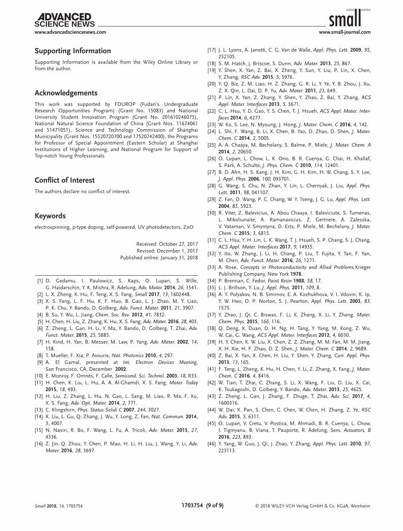
Table 1. Comparison of characteristic parameters of ZnO-based UV detectors.
Photodetector Bias Power density Dark current Photocurrent On–off ratio Rise time Decay time Method Crystalline state
Ref.
ZnO nanofibers 1 V 77.5 µW cm−2 20 pA 6.5 µA 3.3 × 10⁵ ≈100 s ≈50 s Electrospinning Polycrystal [14]
ZnO–CdO nanofibers 1 V 6.54 mW cm−2 – – 104–105 ≈4 s ≈3 s Electrospinning Polycrystal [6]
ZnO:graphdiyne thin film 10 V 0.4 mW cm−2 – – ≈105 6.1 s 2.1 s Spincoating Polycrystal [16]
ZnO homojunction
(Li-doped)−10 V 25 mW cm−2 3.6 µA 19.5 µA 5.4 – – Hydrothermal Monocrystal [23]
ZnO homojunction
(Cu-doped)−5 V 0.25 mW cm−2 112 nA 602 nA 5.4 ≈50 s ≈200 s CVD Monocrystal [22]
ZnO homojunction
(Sb-doped)−3 V 60 mW cm−2 28.3 µA 930 µA 33 15.2 s 20.3 s Hydrothermal Monocrystal [44]
Ag-doped ZnO nanowire – 15-20 mW cm−2 0.1 nA – 52 1.09 s 5 s Electrochemical
deposition
Monocrystal [45]
Sb-doped ZnO nanowire/
Au contact
0 V – 0.1 nA 23 nA 22 0.1 s – CVD Monocrystal [46]
ZnO thin film–Cu nanowires 0 V 0.8 mW cm−2 1 pA 70 pA 70 1 s 30 s Spincoating Polycrystal [41]
1 V 30 pA 2.95 nA 98 10.35 s 2 s
ZnO–SnO2 nanofibers 10 V 0.45 mW cm−2 1.7 pA 7.9 nA 4.6 × 10³ 32.2 s 7.8 s Electrospinning Polycrystal [42]
ZnO ultraporous film 5 V 100 µW cm−2 3.6 nA 1.2 mA 3.3 × 10⁵ 250 s 150 s Fame spray
pyrolysis
Polycrystal [15]
ZnO–PbS nanofibers 10 V 7.02 mW cm−2 – – ≈103 9 s 2 s Electrospinning Polycrystal [43]
ZnO homojunction
nanofibers
0 V 2.5 mW cm−2 0.02 pA 0.5 nA 2.5 × 10⁴ 3.9 s 4.7 s Electrospinning Polycrystal This work
1703754 (9 of 9)
www.advancedsciencenews.com www.small-journal.comsmall
NANO MICRO
© 2018 WILEY-VCH Verlag GmbH & Co. KGaA, WeinheimSmall 2018, 14, 1703754
Supporting InformationSupporting Information is available from the Wiley Online Library or from the author.
AcknowledgementsThis work was supported by FDUROP (Fudan’s Undergraduate Research Opportunities Program) (Grant No. 15083) and National University Student Innovation Program (Grant No. 201610246075), National Natural Science Foundation of China (Grant Nos. 11674061 and 51471051), Science and Technology Commission of Shanghai Municipality (Grant Nos. 15520720700 and 17520742400), the Programs for Professor of Special Appointment (Eastern Scholar) at Shanghai Institutions of Higher Learning, and National Program for Support of Top-notch Young Professionals.
Conflict of InterestThe authors declare no conflict of interest.
Keywordselectrospinning, p-type doping, self-powered, UV photodetectors, ZnO
Received: October 27, 2017Revised: December 1, 2017
Published online: January 31, 2018
[1] D. Gedamu, I. Paulowicz, S. Kaps, O. Lupan, S. Wille, G. Haidarschin, Y. K. Mishra, R. Adelung, Adv. Mater. 2014, 26, 1541.
[2] L. X. Zheng, K. Hu, F. Teng, X. S. Fang, Small 2017, 13, 1602448.[3] X. S. Fang, L. F. Hu, K. F. Huo, B. Gao, L. J. Zhao, M. Y. Liao,
P. K. Chu, Y. Bando, D. Golberg, Adv. Funct. Mater. 2011, 21, 3907.[4] B. Su, Y. Wu, L. Jiang, Chem. Soc. Rev. 2012, 41, 7832.[5] H. Chen, H. Liu, Z. Zhang, K. Hu, X. S. Fang, Adv. Mater. 2016, 28, 403.[6] Z. Zheng, L. Gan, H. Li, Y. Ma, Y. Bando, D. Golberg, T. Zhai, Adv.
Funct. Mater. 2015, 25, 5885.[7] H. Kind, H. Yan, B. Messer, M. Law, P. Yang, Adv. Mater. 2002, 14,
158.[8] T. Mueller, F. Xia, P. Avouris, Nat. Photonics 2010, 4, 297.[9] A. El Gamal, presented at Int. Electron Devices Meeting,
San Francisco, CA, December 2002.[10] E. Monroy, F. Omnès, F. Calle, Semicond. Sci. Technol. 2003, 18, R33.[11] H. Chen, K. Liu, L. Hu, A. A. Al-Ghamdi, X. S. Fang, Mater. Today
2015, 18, 493.[12] H. Liu, Z. Zhang, L. Hu, N. Gao, L. Sang, M. Liao, R. Ma, F. Xu,
X. S. Fang, Adv. Opt. Mater. 2014, 2, 771.[13] C. Klingshirn, Phys. Status Solidi C 2007, 244, 3027.[14] X. Liu, L. Gu, Q. Zhang, J. Wu, Y. Long, Z. Fan, Nat. Commun. 2014,
5, 4007.[15] N. Nasiri, R. Bo, F. Wang, L. Fu, A. Tricoli, Adv. Mater. 2015, 27,
4336.[16] Z. Jin, Q. Zhou, Y. Chen, P. Mao, H. Li, H. Liu, J. Wang, Y. Li, Adv.
Mater. 2016, 28, 3697.
[17] J. L. Lyons, A. Janotti, C. G. Van de Walle, Appl. Phys. Lett. 2009, 95, 252105.
[18] S. M. Hatch, J. Briscoe, S. Dunn, Adv. Mater. 2013, 25, 867.[19] Y. Shen, X. Yan, Z. Bai, X. Zheng, Y. Sun, Y. Liu, P. Lin, X. Chen,
Y. Zhang, RSC Adv. 2015, 5, 5976.[20] Y. Q. Bie, Z. M. Liao, H. Z. Zhang, G. R. Li, Y. Ye, Y. B. Zhou, J. Xu,
Z. X. Qin, L. Dai, D. P. Yu, Adv. Mater. 2011, 23, 649.[21] P. Lin, X. Yan, Z. Zhang, Y. Shen, Y. Zhao, Z. Bai, Y. Zhang, ACS
Appl. Mater. Interfaces 2013, 5, 3671.[22] C. L. Hsu, Y. D. Gao, Y. S. Chen, T. J. Hsueh, ACS Appl. Mater. Inter-
faces 2014, 6, 4277.[23] W. Ko, S. Lee, N. Myoung, J. Hong, J. Mater. Chem. C 2016, 4, 142.[24] L. Shi, F. Wang, B. Li, X. Chen, B. Yao, D. Zhao, D. Shen, J. Mater.
Chem. C 2014, 2, 5005.[25] A. A. Chaaya, M. Bechelany, S. Balme, P. Miele, J. Mater. Chem. A
2014, 2, 20650.[26] O. Lupan, L. Chow, L. K. Ono, B. R. Cuenya, G. Chai, H. Khallaf,
S. Park, A. Schulte, J. Phys. Chem. C 2010, 114, 12401.[27] B. D. Ahn, H. S. Kang, J. H. Kim, G. H. Kim, H. W. Chang, S. Y. Lee,
J. Appl. Phys. 2006, 100, 093701.[28] G. Wang, S. Chu, N. Zhan, Y. Lin, L. Chernyak, J. Liu, Appl. Phys.
Lett. 2011, 98, 041107.[29] Z. Fan, D. Wang, P. C. Chang, W. Y. Tseng, J. G. Lu, Appl. Phys. Lett.
2004, 85, 5923.[30] R. Viter, Z. Balevicius, A. Abou Chaaya, I. Baleviciute, S. Tumenas,
L. Mikoliunaite, A. Ramanavicius, Z. Gertnere, A. Zalesska, V. Vataman, V. Smyntyna, D. Erts, P. Miele, M. Bechelany, J. Mater. Chem. C 2015, 3, 6815.
[31] C. L. Hsu, Y. H. Lin, L. K. Wang, T. J. Hsueh, S. P. Chang, S. J. Chang, ACS Appl. Mater. Interfaces 2017, 9, 14935.
[32] Y. Ito, W. Zhang, J. Li, H. Chang, P. Liu, T. Fujita, Y. Tan, F. Yan, M. Chen, Adv. Funct. Mater. 2016, 26, 1271.
[33] A. Rose, Concepts in Photoconductivity and Allied Problems,Krieger Publishing Company, New York 1978.
[34] P. Brennan, C. Fedor, Paint Resin 1988, 58, 17.[35] L. J. Brillson, Y. Lu, J. Appl. Phys. 2011, 109, 8.[36] A. Y. Polyakov, N. B. Smirnov, E. A. Kozhukhova, V. I. Vdovin, K. Ip,
Y. W. Heo, D. P. Norton, S. J. Pearton, Appl. Phys. Lett. 2003, 83, 1575.
[37] Y. Zhao, J. Qi, C. Biswas, F. Li, K. Zhang, X. Li, Y. Zhang, Mater. Chem. Phys. 2015, 166, 116.
[38] Q. Deng, X. Duan, D. H. Ng, H. Tang, Y. Yang, M. Kong, Z. Wu, W. Cai, G. Wang, ACS Appl. Mater. Interfaces 2012, 4, 6030.
[39] H. Y. Chen, K. W. Liu, X. Chen, Z. Z. Zhang, M. M. Fan, M. M. Jiang, X. H. Xie, H. F. Zhao, D. Z. Shen, J. Mater. Chem. C 2014, 2, 9689.
[40] Z. Bai, X. Yan, X. Chen, H. Liu, Y. Shen, Y. Zhang, Curr. Appl. Phys. 2013, 13, 165.
[41] F. Teng, L. Zheng, K. Hu, H. Chen, Y. Li, Z. Zhang, X. Fang, J. Mater. Chem. C 2016, 4, 8416.
[42] W. Tian, T. Zhai, C. Zhang, S. Li, X. Wang, F. Liu, D. Liu, X. Cai, K. Tsukagoshi, D. Golberg, Y. Bando, Adv. Mater. 2013, 25, 4625.
[43] Z. Zheng, L. Gan, J. Zhang, F. Zhuge, T. Zhai, Adv. Sci. 2017, 4, 1600316.
[44] W. Dai, X. Pan, S. Chen, C. Chen, W. Chen, H. Zhang, Z. Ye, RSC Adv. 2015, 5, 6311.
[45] O. Lupan, V. Cretu, V. Postica, M. Ahmadi, B. R. Cuenya, L. Chow, I. Tiginyanu, B. Viana, T. Pauporte, R. Adelung, Sens. Actuators, B 2016, 223, 893.
[46] Y. Yang, W. Guo, J. Qi, J. Zhao, Y. Zhang, Appl. Phys. Lett. 2010, 97, 223113.