Identification of Potential Novel Biomarkers and Signaling Pathways ...

UNLV Theses, Dissertations, Professional Papers, and Capstones
8-1-2016
Novel Pathways to High-Efficiency Chalcopyrite Photovoltaic Novel Pathways to High-Efficiency Chalcopyrite Photovoltaic
Devices: A Spectroscopic Investigation of Alternative Buffer Devices: A Spectroscopic Investigation of Alternative Buffer
Layers and Alkali-Treated Absorbers Layers and Alkali-Treated Absorbers
Michelle Mezher University of Nevada, Las Vegas
Follow this and additional works at: https://digitalscholarship.unlv.edu/thesesdissertations
Part of the Chemistry Commons
Repository Citation Repository Citation Mezher, Michelle, "Novel Pathways to High-Efficiency Chalcopyrite Photovoltaic Devices: A Spectroscopic Investigation of Alternative Buffer Layers and Alkali-Treated Absorbers" (2016). UNLV Theses, Dissertations, Professional Papers, and Capstones. 2794. http://dx.doi.org/10.34917/9302951
This Dissertation is protected by copyright and/or related rights. It has been brought to you by Digital Scholarship@UNLV with permission from the rights-holder(s). You are free to use this Dissertation in any way that is permitted by the copyright and related rights legislation that applies to your use. For other uses you need to obtain permission from the rights-holder(s) directly, unless additional rights are indicated by a Creative Commons license in the record and/or on the work itself. This Dissertation has been accepted for inclusion in UNLV Theses, Dissertations, Professional Papers, and Capstones by an authorized administrator of Digital Scholarship@UNLV. For more information, please contact [email protected].
NOVEL PATHWAYS TO HIGH-EFFICIENCY CHALCOPYRITE PHOTOVOLTAIC
DEVICES: A SPECTROSCOPIC INVESTIGATION OF ALTERNATIVE BUFFER
LAYERS AND ALKALI-TREATED ABSORBERS
By
Michelle Mezher
Bachelor of Arts – Chemistry (ACS Accredited) University of San Diego
2012
A dissertation submitted in partial fulfillment of the requirements for the
Doctor of Philosophy – Chemistry
Department of Chemistry and Biochemistry College of Sciences
The Graduate College
University of Nevada, Las Vegas August 2016

Copyright 2016 by Michelle Mezher
All Rights Reserved

ii
Dissertation Approval
The Graduate College
The University of Nevada, Las Vegas
June 3, 2016
This dissertation prepared by
Michelle Mezher
entitled
Novel Pathways to High-Efficiency Chalcopyrite Photovoltaic Devices: A Spectroscopic
Investigation of Alternative Buffer Layers and Alkali-Treated Absorbers
is approved in partial fulfillment of the requirements for the degree of
Doctor of Philosophy – Chemistry
Department of Chemistry and Biochemistry
Clemens Heske, Ph.D. Kathryn Hausbeck Korgan, Ph.D. Examination Committee Chair Graduate College Interim Dean
Kathleen Robins, Ph.D. Examination Committee Member
David Hatchett, Ph.D. Examination Committee Member
Shubhra Bansal, Ph.D. Graduate College Faculty Representative

iii
ABSTRACT
Novel Pathways to High-Efficiency Chalcopyrite Photovoltaic Devices:
A Spectroscopic Investigation of Alternative Buffer Layers and Alkali-treated Absorbers
By
Michelle Mezher
Dr. Clemens Heske, Examination Committee Chair
Professor of Chemistry
University of Nevada, Las Vegas
Within the past few years, breakthroughs in Cu(In,Ga)Se2 (CIGSe) thin-film photovoltaic
device efficiencies (on a laboratory scale) were achieved utilizing alkali-treated (KF)
absorbers. Na incorporation in the CIGSe absorber, either diffused from the substrate or
deliberately deposited, affects the surface electronic properties of the CIGSe absorber.
The role of Na, however, is still not fully understood with some studies suggesting that Na
also passivates defects at the grain boundaries. Replacing Na with K offered an efficiency
boost resulting in KF treatments becoming the new “hot topic” in the chalcopyrite field,
both in terms of understanding how the treatment changes the absorber along with
studying the differences between alternative KF deposition methods. To provide insight
on these issues, x-ray (XPS) and ultraviolet (UPS) photoelectron spectroscopy, inverse
photoemission spectroscopy (IPES), as well as x-ray emission spectroscopy (XES) are
utilized to investigate two sample sets. The first set (Chapter 4) compares the effects of
both KF and NaF treatments on absorbers taken from the production line of STION and
the National Renewable Energy Laboratory. The purpose here is to compare how similar
alkali-treatments affect chalcopyrite devices from different sources along with comparing

iv
the alkali-treatments themselves. The second sample set (Chapter 5) investigates effects
of KF treatments when incorporated utilizing different deposition techniques.
The most recent world record efficiency for CIGSe thin-film devices was not
achieved with the KF-treatment, but with the replacement of the traditional CdS buffer
layer (between the absorber and transparent front electrode) with Zn(O,S), a material
offering the possibility of increasing the current collection in the shorter wavelength region
of the solar spectrum. To further optimize these photovoltaic devices, an understanding
of the interactions between the absorber and the buffer layer is crucial. For example,
record CdS/CIGSe devices have a flat conduction band alignment at the buffer/absorber
interface, while, in contrast, the less efficient CdS/Cu(In,Ga)S2 device exhibits a cliff-like
conduction band offset, impeding electron transport. Thus, a determination of the
conduction band offset is, among other aspects, of significant importance.
When using Zn(O,S) as the buffer layer, it should be noted that the bandgap of a
Zn(O,S) alloy exhibits a strong bowing effect as the O:S ratio varies. With the ability to
change the O:S ratio and alter the bandgap, it is thus important to understand the
chemical and electronic structure of the Zn(O,S)/CIGSe interface in high-efficiency
devices through direct and independent analysis of the heterojunction formation, the
valence band, and the conduction band. This is the first non-destructive analysis of the
interface using XPS, UPS, IPES, and XES investigating samples with varying buffer layer
thickness. A comprehensive and all-experimental depiction of the electronic level
alignment (Chapter 6) and chemical interactions (Chapter 7) at the interface will be
presented.

v
ACKNOWLEDGEMENTS
First and foremost, I would like to thank my advisor and mentor, Dr. Clemens Heske. I will
always be extremely grateful that you have provided me with the amazing opportunity of
pursuing a deeper knowledge in chemistry/physics and spectroscopy. You have been
patient and kind and instilled within me the drive to always understand why and not take
things at face-value. You have taught me to articulate my thoughts more clearly and
guided me to become a better scientist throughout my graduate years. Thank you.
Drs. Lothar Weinhardt, Moni Blum, and Marcus Bär – I am very thankful for the
guidance and lessons you have offered me at the beamline, through e-mail, and in the
labs at UNLV and HZB. I count myself lucky to have been taught by scientists top in their
field.
Drs. Kim Horsley and Doug Duncan – Your friendships both inside and outside the
lab have really made living in Vegas better after moving away from everyone I knew. From
our gif conversations, rock climbing adventures, and love of ayce sushi, these friendships
will have a lasting impact on my life. I look forward to you guys moving to San Diego ;).
I will always be grateful for past and present group members that have shared in
the love/hate relationship of lab maintenance and providing valuable friendships and
memorable discussions – Drs. Timo Hofmann, Samantha Rosenberg, Dirk Hauschild,
Manuela Wallesch, and Kyle Bowen; Lynette Kogler, James Carter, Kyle Aleshire, Chase
Aldridge, Ryan Bugni, and Sarah Alexander.
Dr. Moni Blum, Dr. Dagmar Kreikemeyer-Lorenzo, and Andi Benkert – Beamtime
buddies! I will miss our night-shift yoga sessions at the beamline, learning “the cup song”,
pitch perfect, and all of our fun adventures together!

vi
Drs. Regan Wilks, David Starr, and Jan Alsmeier, Evelyn Handick, and Leo Köhler
– You guys have made my time and experience in Berlin so much fun. Thank you for
helping me with the process of moving to Berlin, showing me the culture, teaching me in
lab, and accepting me as part of the Bär group. Regan – I’m waiting for the next time we
hang out and drink some delicious beer! Dublin would be a good place .
I’m thankful for collaborators on the F-PACE project, Dr. Kannan Ramanathan, Dr.
Lorelle Mansfield, Dr. Rebekah Garris, and Dr. Chris Muzzillo, that have provided me with
fun samples to measure and their guidance throughout the project and during HOPE.
I’m thankful for Eric Knight and all his help keeping the lab running, Wanli Yang for
maintaining the beamline, Mark Miyamoto and Debbie Masters for your skills and helping
me with all the fun administrative tasks, and of course my committee (past and present),
Dr. Kathy Robins, Dr. David Hatchett, Dr. Rama Venkat, Dr. Shubhra Bansal, and Dr.
Dennis Lindle for putting in your time and offering your guidance throughout my graduate
years.
My family, Mom and Dad – I can never put into words how much I appreciate all
the hard work and sacrifices you have made to make sure Andrew and I received a good
education. You have lived your lives always setting good examples for Andrew and
myself. Thank you for all your support. Andrew – Our competitive streak of always
needing to outdo each other academically has led to this exact moment: Look at me. I’m
the real doctor now.
Jeff George (“Professional Scientist”) – For the past four years you have been a
constant support in all aspects of my life. Thank you for always being the optimism to my
pessimism and encouraging me to be my best.

vii
My aerial family at SHINE and PFS, thank you for keeping me sane and providing
valuable and memorable friendships. In addition, thank you for making sure I didn’t fall
and die when suspended in the air or playing on the apparatuses. I think that’s also
important .
Last, but definitely not least, my favorite furry companion, Raja – Meow.
No man can reveal to you aught but that which already lies half asleep in the dawning of your knowledge. The teacher who walks in the shadow of the temple, among his followers, gives not of his wisdom but rather of his faith and his lovingness. If he is indeed wise he does not bid you enter the house of his wisdom, but rather leads you to the threshold of your own mind.
― Kahlil Gibran, The Prophet

viii
DEDICATION
In memory of Dennis Lindle, Jiddo Khalil, Khalo Zouzou, and Charles Ghawi
For my family in Lebanon

ix
TABLE OF CONTENTS ABSTRACT ................................................................................................................. iii
ACKNOWLEDGEMENTS ............................................................................................. v
DEDICATION .............................................................................................................. vii
LIST OF TABLES ........................................................................................................ x
LIST OF FIGURES .......................................................................................................xi
CHAPTER 1 INTRODUCTION .......................................................................... 1
CHAPTER 2 STRUCTURE OF THE CIGSe THIN-FILM SOLAR CELL 2.1 Formation of a p-n Junction..................................................... 5
2.2 CIGSe Substrate and Absorber Structure .............................. 6
2.2.1 CIGSe substrate and back-contact ........................... 6
2.2.2 CIGSe absorber ....................................................... 8
2.2.3 Alkali-incorporation in CIGSe ................................. 10
2.3 Buffer Layers ......................................................................... 12
2.3.1 CdS ........................................................................ 12
2.3.2 Zn(O,OH,S) ............................................................ 12
2.3.3 Electronic band-alignments .................................... 14
2.4 Window Layers ...................................................................... 16
CHAPTER 3 SPECTROSCOPIC TECHNIQUES
3.1 Introduction .......................................................................... 18
3.2 Lab-based Spectroscopies ................................................... 19
3.2.1 X-ray Photoelectron Spectroscopy (XPS) ............... 19
3.2.2 X-ray-excited Auger Electron Spectroscopy (AES) 21
3.2.3 Ultra-violet Photoelectron Spectroscopy (UPS) ...... 21
3.2.4 Inverse Photoemission Spectroscopy (IPES) ......... 23
3.2.5 Combining UPS and IPES ...................................... 23
3.2.6 Surface Sensitivity .................................................. 24
3.2.7 Peak Fitting ............................................................ 26
3.3 Sample Preparation and Measurement Parameters ........... 27
3.4 Synchrotron-Based Soft X-ray Spectroscopy ....................... 31
3.4.1 X-ray Emission (XES) ............................................. 31
3.4.2 Beamline Description .............................................. 33
CHAPTER 4 CHEMICAL AND ELECTRONIC SURFACE PROPERTIES OF
ALKALI-TREATED CIG(S)Se ABSORBERS: COMPARISON OF
INDUSTRY (STION) TO NATIONAL LAB (NREL) ABSORBERS

x
4.1 Introduction .......................................................................... 35
4.2 Experimental Details ............................................................ 36
4.3 Results and Discussion ......................................................... 38
4.4 Conclusion ........................................................................... 61
CHAPTER 5 KF COEVAPORATION VS. KF POST DEPOSITION TREATMENT:
SPECTROSCOPIC INVESTIGATION ON THE EFFECTS OF KF
FOLLOWING DIFFERENT DEPOSITION PROCESSES
5.1 Introduction .......................................................................... 63
5.2 Experimental Details ............................................................ 63
5.3 Results and Discussion ........................................................ 65
5.4 Conclusion ........................................................................... 93
CHAPTER 6 ELECTRONIC STRUCTURE OF THE Zn(O,S)/CIGSe INTERFACE
6.1 Introduction .......................................................................... 95
6.2 Experimental Details ............................................................ 96
6.3 Results and Discussion ........................................................ 98
6.4 Conclusion ......................................................................... 105
CHAPTER 7 SOFT X-RAY SPECTROSCOPY OF A COMPLEX
HETEROJUNCTION IN HIGH-EFFICIENCY THIN-FILM
PHOTOVOLTAICS: INTERMIXING AND Zn SPECIATION AT THE
Zn(O,S)/CIGSe INTERFACE
7.1 Introduction ........................................................................ 106
7.2 Experimental Details .......................................................... 107
7.3 Results and Discussion ...................................................... 108
7.4 Conclusion ......................................................................... 123
CHAPTER 8 SUMMARY ................................................................................. 124
APPENDIX LIST OF ABBREVIATIONS AND SYMBOLS ............................. 127
REFERENCES .......................................................................................................... 129
CURRICULUM VITAE .............................................................................................. 141

xi
LIST OF TABLES Table 1: Core level peak positions of the bare absorber, the thin (5 min)
Zn(O,S)/CIGSe sample, and the thick (22.5 min) Zn(O,S)/CIGSe sample,
as well as their relative shifts ............................................................... 102

xii
LIST OF FIGURES
Figure 2.1: Schematic of the band alignment p-n junction diagram and semiconductor
to metal interface. .................................................................................... 5
Figure 2.2: SEM cross-section of a typical CIGSe solar cell fabricated at NREL. Ref.
from 8. ...................................................................................................... 7
Figure 2.3: Metal flux schematic for the three-stage coevaporation process. Taken from
ref. 19. ...................................................................................................... 8
Figure 2.4: Schematics of various Na-treated CIGSe absorbers including a) diffusion
from the soda-lime glass, b) Na barrier and NaF precursor, c) NaF
coevaporated with CIGSe, and d) NaF PDT. ......................................... 11
Figure 2.5: Optical bandgap as a function of O:S ratio in a Zn(O,S) allow. Taken from
ref. 57 ..................................................................................................... 13
Figure 2.6: Schematic of several band alignment scenarios a) flat b) spike or c) cliff
configuration for the conduction band offset. ......................................... 15
Figure 2.7: Example of a CIGSe minimodule deposited onto a flexible substrate from
EMPA. Ref. from 75. .............................................................................. 16
Figure 3.1: Schematic of a) x-ray photoelectron spectroscopy (XPS) and b) x-ray Auger
electron spectroscopy (XAES) transitions .............................................. 20
Figure 3.2: Schematic of a) ultra-violet photoelectron spectroscopy (UPS) and b)
inverse photoemission spectroscopy (IPES) transitions. ....................... 22
Figure 3.3: The “Universal Curve” (line that averages the experimental data points)
presents the relationship of the inelastic mean free path of electrons as a
function of their kinetic energy relative to vacuum level. Adapted from
reference88 ............................................................................................. 25
Figure 3.4: Mg Kα survey spectra of the Cu(In0.7,Ga0.3)Se2 absorber as a function of
treatment time during a low-energy ion cleaning series. Spectra in the blue
box are shown on an enlarged energy axis in Fig. 3.5 ........................... 28

xiii
Figures 3.5: XPS spectra of the low binding energy region before and after two low-
energy ion treatment steps. ................................................................... 29
Figure 3.6: UPS and IPES spectra showing the band gap edge positions (VBM and
CBM) as well as the electronic surface bandgap of the CIGSe absorber as
a function of treatment time ................................................................... 30
Figure 3.7: Schematic of x-ray emission spectroscopy (XES) transitions. The “zero” step
of the process is colored gray while the XES process is in red .............. 31
Figure 3.8: The fluorescence and Auger yields for the K subshell as a function of Atomic
number. Ref. from 97, 98 ....................................................................... 32
Figure 3.9: Schematic of Beamline 8.0.1 at the Advanced Light Source. Taken from ref.
99 ............................................................................................................ 34
Figure 4.1: XPS survey spectra normalized to the In5/2 peak area of the NREL and
STION bare absorbers (black), both NaF-treated absorbers (red), both low
efficiency KF-treated absorbers (blue), and both high efficiency KF-treated
absorbers (pink) ..................................................................................... 38
Figure 4.2: XPS detailed spectra of the Cu 2p3/2 peak normalized to the In5/2 peak area
(left) and to Cu 2p3/2 peak height (right) of the NREL and STION bare
absorbers (black), NaF-treated absorbers (red), and low and high efficiency
KF-treated absorbers (blue, pink). ......................................................... 40
Figure 4.3: XPS detailed spectra of the Ga 2p3/2 peak normalized to the In5/2 peak area
(left) and to Ga 2p3/2 peak height (right) of the NREL and STION bare
absorbers (black), NaF-treated absorbers (red), and low and high efficiency
KF-treated absorbers (blue, pink). ......................................................... 41
Figure 4.4: XPS detailed spectra of the Ga LMM Auger peak normalized to the In 3d5/2
peak area (left) and to Ga LMM peak height (right) of the NREL and STION
bare absorbers (black), NaF-treated absorbers (red), and low and high
efficiency KF-treated absorbers (blue, pink). ......................................... 42
Figure 4.5: XPS detailed spectra of the Ga 3d / In 4d region of the NREL bare absorber
(top left), NaF-treated absorber (top right), and low and high efficiency KF-
treated absorbers (bottom left and right). ............................................... 44

xiv
Figure 4.6: XPS detailed spectra of the Ga 3d / In 4d region of the STION bare absorber
(top left), NaF-treated absorber (top right), and low and high efficiency KF-
treated absorbers (bottom left and right). ............................................... 45
Figure 4.7: XPS detailed spectra of the Se 3d peak normalized to the In 3d5/2 peak area
(left) and to Se 3s peak height (right) of the NREL and STION bare
absorbers (black), NaF-treated absorbers (red), and low and high efficiency
KF-treated absorbers (blue, pink). The S 2s peak intensity for the STION
absorbers changes as a function of alkali-treatment. ............................. 47
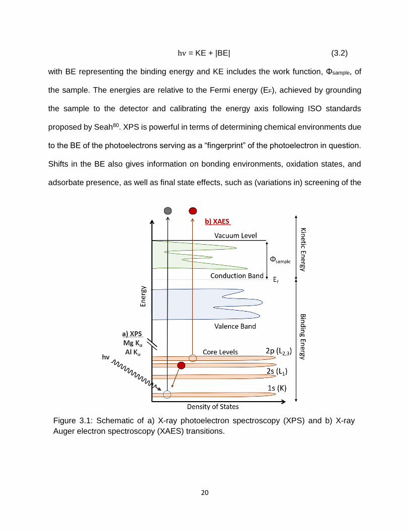
Figure 4.8: XPS detailed spectra of the In 3d5/2 peak (left) and the In MNN (right)
normalized to peak height of the NREL and STION bare absorbers (black),
NaF-treated absorbers (red), and low and high efficiency KF-treated
absorbers (blue, pink). ........................................................................... 48
Figure 4.9: XPS detailed spectra of the K 2p peak (left). A closer look at the K 2p for
the NREL absorbers is shown at the right along with K references. ...... 49
Figure 4.10: XPS detailed spectra of the Na 1s (left) and O 1s peaks (right) normalized
to the In5/2 peak area of the NREL and STION bare absorbers (black), NaF-
treated absorbers (red), and low and high efficiency KF-treated absorbers
(blue, pink). ............................................................................................ 50
Figure 4.11: Modified Auger Parameter plot of Na 1s and Na KLL. The ion treated data
are shown in red with references (111,112) in black. ............................. 52
Figure 4.12: XPS detailed spectra of the F 1s (left) and F KLL (right) peaks of the NREL
and STION bare absorbers (black), NaF-treated absorbers (red), and low
and high efficiency KF-treated absorbers (blue, pink). ........................... 53
Figure 4.13: XPS spectra of the Zn 2p peaks for the NREL (left) and STION (right) bare
absorbers (black), NaF-treated absorbers (red), and low and high efficiency
KF-treated absorbers (blue, pink). ......................................................... 54
Figure 4.14: UPS spectra taken with He II excitation of the NREL and STION bare
absorbers (black), NaF-treated absorbers (red), and low and high efficiency
KF-treated absorbers (blue, pink). ......................................................... 56
Figure 4.15: XES emission spectra excited nonresonantly with 180 eV of the S L2,3
region for the STION bare (black), NaF-treated (red), and low and high

xv
efficiency KF-treated absorbers (blue, pink). Reference spectra are
provided for comparison. ....................................................................... 58
Figure 4.16: Relative weights of the STION bare absorber spectrum was subtracted from
the alkali-treated absorber spectra and the resulting residuals are presented
with reference spectra. Multiplication factors shown. ............................ 59
Figure 4.17: XES emission spectra of the K L2,3 (left) and F Kα of the NREL and STION
bare absorbers (black), NaF-treated absorbers (red), and low and high
efficiency KF-treated absorbers (blue, pink). ......................................... 60
Figure 5.1: XPS Mg Kα survey spectrum taken of the NREL bare and KF-treated
absorbers. The ion-treated surfaces are shown in black, while the rinsed
surfaces are shown in red ...................................................................... 65
Figure 5.2: Detailed XPS Mg Kα spectra of the Cu 2p3/2 taken on the ion-treated (center)
and NH4OH treated (top) of the CKIGSe, both CIGSe, and both KF PDT
absorbers. This is compared to a previous sample set, displayed on the
bottom (four alkali-treated NREL absorbers, grown with the three-stage
coevaporation process). ......................................................................... 66
Figure 5.3: Detailed XPS Mg Kα spectra of the Se 3d region, normalized by In 3d5/2 area
(left) and peak height (right). The ion-treated spectra are shown at the
bottom, and the NH4OH treated spectra at the top. The expected locations
for oxide contributions are indicated. ..................................................... 67
Figure 5.4: Detailed XPS Mg Kα spectra of the In 3d5/2 (left) and In MNN (right) regions,
normalized by peak height. The ion-treated spectra are shown at the
bottom, while the NH4OH-treated spectra are at the top. The expected
locations for oxide, selenide, and fluoride contributions are indicated. .. 68
Figure 5.5: Detailed XPS Mg Kα spectra In MNN region, normalized by peak height, for
the clean and rinsed KF PDT absorbers. Three In-Se references are used
to fit the peaks to show contributions from In-F, In-O, and In-Se species.
The residual is shown on the bottom in purple. ...................................... 69
Figure 5.6: Detailed XPS Mg Kα spectra of the Ga 2p3/2 (left) and Ga LMM (right)
regions, normalized by the In 3d5/2 area. The ion-treated spectra are shown
at the bottom, while the NH4OH-treated spectra are at the top. The expected
locations for oxide, selenide, and fluoride contributions are indicated ... 71

xvi
Figure 5.7: Detailed XPS Mg Kα spectra of the Ga 3d and In 4d region. The dotted
spectra represent NH4OH treated absorbers while the continuous line
spectra represent the “clean” surfaces. Regions where Ga 3d and In 4d
peaks are located are boxed. ................................................................. 72
Figure 5.8: XPS detail spectra of the Ga 3d/In 4d of the pre and post-rinse CIGSe
absorber (top) and CIGSe/SiO2 (bottom). Fit curves for In:Ga contributions
to the peak are shown along with their respective residuals (purple). .... 73
Figure 5.9: XPS detail spectra of the Ga 3d/In 4d region of the CKIGSe absorber pre-
rinse (left) and post-rinse (right). Fit curves for In:Ga contributions to the
peak are shown along with their respective residuals (purple). .............. 74
Figure 5.10: XPS detail spectra of the Ga 3d/In 4d region of the pre and post-rinse KF
PDT absorber (top) and KF PDT/SiO2 (bottom). Fit curves for In:Ga
contributions to the peak are shown along with their respective residuals
(purple) .................................................................................................. 76
Figure 5.11: XPS detail spectra of the Ga 3d/In 4d region of the pre-rinse KF PDT
absorber as a function of fit curves to show the process of determining a
good fit. Fit curves for In:Ga (In 4d5/2, In 4d3/2, Ga 3d5/2, Ga 3d3/2)
contributions to the peak are shown along with their respective residuals
(purple). ................................................................................................. 78
Figure 5.12: Detailed XPS Mg Kα spectra of the F 1s region, normalized by the In 3d5/2
area. The ion-treated spectra are shown at the bottom, while the NH4OH-
treated spectra are at the top (left). The right graph is scaled to see the F 1s
peaks of the NH4OH treated absorbers (only). The expected locations for
InF3, NaF, KF, and CF3 contributions are indicated. ............................... 80
Figure 5.13: Detailed XPS Mg Kα spectra of the C 1s and K 2p region, normalized by the
In 3d5/2 area (left). The ion-treated spectra are shown at the bottom, while
the NH4OH-treated spectra are at the top (left). The right graph is magnified
to show the K 2p peaks of the NH4OH and ion-treated absorbers. The
expected locations for Ga LMM, KF, and metallic K (Kmet) are indicated..81
Figure 5.14: Detailed XPS Mg Kα spectra of the Na 1s region, normalized by the In 3d5/2
area. The ion-treated spectra are shown at the bottom, while the NH4OH-
treated spectra are at the top (left). The right graph is scaled to show the

xvii
Na 1s peaks of the NH4OH-treated absorbers (only). A line was drawn to
help guide the eye. On the left, the expected locations for NaF and NaO
contributions are indicated. .................................................................... 83
Figure 5.15: Modified Auger Parameter plot of Na 1s and Na KLL. The ion-treated data
are shown in red, NH4OH treated data in blue, and references (111,112) in
black. ..................................................................................................... 85
Figure 5.16: Detailed XPS Mg Kα spectra of the O 1s region, normalized by the In 3d5/2
area (left) and O 1s peak height (right). The ion-treated spectra are shown
at the bottom, while the NH4OH-treated spectra are at the top. The
expected locations for water, hydroxide, metal oxides, and carbonates are
indicated ................................................................................................ 86
Figure 5.17: XPS detail spectra of the O 1s peak and fit (components in black, sum in
red) of the pre and post-rinsed CIGSe (top) and CIGSe/SiO2 samples
(bottom). ................................................................................................ 87
Figure 5.18: XPS detail spectra of the O 1s peak and fit (components in black, sum in
red) of the pre and post-rinsed KF PDT (top) and KF PDT/SiO2 samples
(bottom).. ............................................................................................... 88
Figure 5.19: XPS detail spectra of the O 1s peak and fit (components in black, sum in
red) of the pre and post-rinsed CKIGSe sample. ................................... 89
Figure 5.20: UPS (He II) and IPES spectra of all absorbers. A Savitzky-Golay smooth
line is used as a guide to the eye. .......................................................... 90
Figure 5.21: UPS (He II) and IPES spectra of all absorbers. The ion-treated surfaces are
shown in black, while the rinsed surfaces are shown in red. .................. 92
Figure 6.1: XPS detail spectra of the O 1s peak and fit (components in black, sum in
red) of a) the thin (5 min) and b) the thick (22.5 min) Zn(O,S)/CIGSe
samples. The magnified residual of each fit is also shown. ................... 99
Figure 6.2: He I UPS (left) and IPES (right) spectra of the bare CIGSe absorber (bottom)
and the thick Zn(O,S)/CIGSe sample (top). VBM and CBM values
determined by linear extrapolations of the leading edges (red lines) are
shown, together with the resulting electronic surface band gaps. Error bars
are ±0.10 and ±0.15 eV for the VBM and CBM determination, respectively.

xviii
A Savitzky-Golay-smoothed line is shown for the IPES spectra as a guide to
the eye. ................................................................................................ 100
Figure 6.3: Band alignment scheme of the Zn(O,S)/CIGSe interface. The band edge
positions at the CIGSe and Zn(O,S) surfaces are shown on the left and
right, respectively. In the center, the band alignment at the interface is
shown, taking interface-induced band bending changes at the absorber
surfaces and band bending in the buffer layer into account (as indicated
by the ovals). ....................................................................................... 104
Figure 7.1: XPS survey spectra of the untreated (black) and ion treated (red)
Zn(O,S)/CIGSe sample series: CIGSe bare absorber (bottom), 5 min
Zn(O,S) (middle), and 22.5 min Zn(O,S) (top). .................................... 109
Figure 7.2: Modified Auger Parameter plot of Na 1s is shown before (red dot) and after
different 50 eV Ar+-ion energy treatment steps (red triangles) in comparison
to references (111,112) in black (error bars are ±0.05 eV on both axes).
............................................................................................................. 110
Figure 7.3: Mg Kα XPS spectra of the Se 3d peak (left) and the Ga 3d/In 4d region
(right) for the CIGSe bare absorber and Zn(O,S)/CIGSe samples of varying
thickness. To describe the 10 and 22.5 min spectra, the result of a fit with
the CIGSe lineshape and a linear background is shown. Multiplication
factors are shown in parentheses. ....................................................... 112
Figure 7.4: Effective Zn(O,S) layer thickness derived from Se 3d (blue), Ga 3d (red, 5
min), In 4d (green, 5 min), Ga 3d/In 4d combined (pink, 10 min) and nominal
thickness (black) as a function of Zn(O,S) CBD time. The 10 min nominal
thickness and Ga 3d/In 4d data were shifted slightly to differentiate between
the data points ..................................................................................... 114
Figure 7.5: XPS detail spectra of the Ga 3d/In 4d region of the CIGSe absorber (bottom)
and 5 min Zn(O,S) (top). Fit curves for In:Ga contributions to the peak are
shown along with their respective residuals (purple). .......................... 115
Figure 7.6: (Left) XPS spectra of the 22.5 min Zn(O,S) O 1s peak as a function of ion
treatment time. (Right) Fits of the O 1s peak show a change in OH/OH+O
ratio as a function of ion treatment ....................................................... 117

xix
Figure 7.7: XPS spectra of the Zn 2p3/2 peak (left) and S 2p/Se 3p peak (right) for the 5
and 22.5 min Zn(O,S) samples. Reference peak positions (111,112) are
indicated above both peak ................................................................... 119
Figure 7.8: (Left) S L2,3 and Se M2,3 emission of the Zn(O,S)/CIGSe interface as a
function of CBD time and a ZnS reference. Multiplication factors shown in
parenthesis .......................................................................................... 121
Figure 7.9: a) Difference spectra from subtracting the 22.5 min Zn(O,S) S L2,3 emission
from the 5 min (red) and 10 min(blue) spectra. b) Reference spectra for
comparison .......................................................................................... 122

1
CHAPTER 1
INTRODUCTION In 1954, the commercial solar age began with the realization that Si semiconductors
exhibited photoelectric properties, leading to the development of a Si solar cell with a 6%
energy conversion 1. Over the next 60 years, continued improvements in device
performance have resulted in crystalline and multi-crystalline single-junction Si
photovoltaics (PV) achieving 25.6% (± 0.5) and 20.8% (± 0.5) efficiencies on a laboratory
scale, respectively 2. During the 1970’s and 1980’s, it was shown that in addition to Si,
thin-film chalcogens demonstrated conversion efficiencies over 10% proving that high
efficiency photovoltaic devices did not need to be Si based, but instead consist of two
semiconductor layers with minimal lattice mismatch, suitable conductivity, and minimal
interfacial energy barriers 3. Overtime, these devices have surpassed the efficiency of
multi-crystalline Si-based devices with CdTe at 21.5% (± 0.4), and Cu(In,Ga)Se2 (CIGSe)
at 22.3% on a laboratory scale, which, however, is still well below their theoretical
maximum efficiency 2,4. In 1961, William Shockley and Hans J. Queisser formulated an
upper theoretical limit for the conversion efficiency of a single p-n junction solar cell called,
surprisingly, the Shockley-Queisser limit 5. By considering blackbody radiation, radiative
recombination, and spectrum losses, they calculated that a single-junction solar cell (with
a band-gap around 1.1 eV) has a theoretical maximum efficiency of 30% 5. If the device
were to have a tandem structure of multiple cells, the efficiencies can surpass the
Shockley-Queisser limit, with a three-junction tandem cell exhibiting a theoretical
efficiency of 63% with the highest light concentration 6. Improving the efficiency of a

2
single-junction solar cell will thus in turn improve more complex photovoltaic-based
technologies.
Not only do CdTe and CIGSe solar cells have room for improvement, but there is
also a large disparity between lab-based cells and industry-manufactured full-scaled
modules. For example, the record CIGSe module, held by MiaSole, is 15.7% (± 0.5), only
about half the theoretical maximum efficiency of a single-junction CIGSe solar cell 2,5. In
addition to conversion efficiency, the cost of production is very important, as the only way
solar energy will be competitive in the market is if it is affordable. While crystalline and
multi-crystalline Si are high in module efficiency (22.9% and 18.5% respectively), they are
very expensive to manufacture prompting a cheaper option, amorphous Si (a-Si), to
dominate the solar market despite a low module efficiency of 12.3% (± 0.3) 2. In order to
make CIGSe and CdTe more competitive in the solar market, cheaper deposition
methods and higher module efficiency is imperative.
In this dissertation, the impact of novel deposition parameters on both industry-
manufactured and lab-based Cu(In,Ga)(S,Se)2 (CIGSSe) and CIGSe are investigated in
order to offer understanding on their impact to the chemical and electronic properties of
the absorber surface/interfaces and give insight to their effect on the cell efficiency.
Industry samples are from the STION production line while lab-based samples are from
the National Renewable Energy Lab (NREL) in Golden, CO. This chapter, Chapter 1,
gives a brief introduction and motivation for this research as well as an outline for the
organization of the dissertation. Chapter 2 discusses photovoltaics and how they operate
in-depth with relevant background information on thin-film CIGSe photovoltaics. Chapter

3
3 discusses the methods used to analyze the surface and interfaces of the CIGSe
samples in order to provide a better understanding of the data analysis.
With K incorporated CIGSe devices being the “hot” topic, chapters four and five
investigate the effects of alkali-treatments on chalcopyrite absorbers. Chapter four
focuses on the chemical and electronic surface properties of NaF and KF treated
CIG(S)Se absorbers with a focus on comparing industry grade absorbers and laboratory
deposited absorbers. XPS is used to analyze changes in chemical states and how NaF
and KF alter the surface. UPS gives insight to how the valence band maximum (VBM)
changes with the alkali-treatments. XES offers a more bulk sensitive chemical view of the
treated absorbers. Different alkali-treatments result in devices with very different
conversion efficiencies.
Chapter 5 focuses on different deposition techniques of KF onto the CIGSe. A KF
post deposition treatment is compared to KF that is co-evaporated while the CIGSe
absorber is grown. Because the samples are rinsed before the buffer layer is deposited,
the unrinsed and rinsed surfaces of these samples are compared to see how an ammonia
treatment alters the surface. XPS studies and XES study the chemical changes between
the samples (both rinsed and unrinsed) while UPS and IPES are used to study electronic
structure differences. The different KF deposition techniques result in different conversion
efficiencies of completed twin samples.
Another “hot” topic for chalcopyrites is the use of more-transparent alternative
buffer layers to CdS. Chapters 6 and 7 investigate the electronic and chemical properties
of Zn(O,S), the new alternative buffer layer that lead to the new CIGSSe world efficiency
record of 22.3%4. XPS and XES are used to look at the chemical interactions at the

4
Zn(O,S)/CIGSe interface while XPS, UPS, and IPES are used to probe the electronic
structure of the buffer/absorber interface. These findings are compared to the standard
high efficiency CdS/CIGSe system. The dissertation is then brought to a close with a
summary of the work in Chapter 8.

5
CHAPTER TWO
STRUCTURE OF THE CIGSe THIN-FILM SOLAR CELL
The following chapter provides an overview of the traditional p-n junction in solar cells
and the structure and characteristics of CIGSe thin-film photovoltaics. Some of the
deposition information was received from Lorelle Mansfield and Rebekah Garris during
the HOPE (Hands-On Photovoltaics Experience) workshop at NREL while creating a
standard high-efficiency (18.5%) CIGSe device. Their contributions to this work are
gratefully acknowledged.
2.1 – FORMATION OF A TRADITIONAL p-n JUNCTION Photovoltaic devices convert the sun’s energy into electricity by relying on the
photoelectric effect, which describes the ability of matter to eject electrons when it is
excited by photons. Photons, fundamental particles of light, are absorbed in the
semiconductor material when their energy, hv, is equal to or greater than the energy of
the bandgap, resulting in the creation of electron-hole pairs. If the photon does not have
Figure 2.1: Schematic of the band alignment p-n junction diagram and semiconductor
to metal interface.
CBM
VBM+ + ++
EF
Metalback-contact
Towards front-contact
Eg
n-type p-type

6
enough energy, it would simply pass through the photovoltaic material as if it were
transparent. In order to prevent the recombination of the electron-hole pairs, a built-in
electric field in the solar cell is imperative. To create this electric field, a p-n junction is
formed by contacting a material with holes as the majority carrier (p-type) to a material
with electrons as the majority carrier (n-type), as seen in Figure 2.1. The p-n junction
displayed in the figure is at equilibrium, represented by a flat EF (Fermi energy) spanning
the materials. EF is the statistical average of occupied and unoccupied states and thus,
for an n-type semiconductor EF lies in the bandgap (Eg) closer to the conduction band
minimum (CBM) while for a p-type semiconductor, EF lies closer to the valence band
maximum (VBM). A depletion region forms at the junction due to space charge buildup
causing band-bending to occur7. An electric field, acting as a diode, separates the p-type
and n-type region, allowing electrons to flow towards the front-contact and the holes to
flow toward the back-contact. Attaching metal conductors to the p-type and n-type
materials (front-contact and back-contact) allows an electrical circuit to form after
attaching a load, thus capturing the electrons (electric current) and providing electricity to
power the load.
2.2 – CIGSe SUBSTRATE AND ABSORBER STRUCTURE 2.2.1 – Substrate and back-contact The majority of CIGSe solar cells are fabricated to incorporate the same basic structure
represented by the Scanning Electron Microscopy (SEM) cross-section of the device in
Figure 2.28 The substrate of CIGSe is typically glass, however flexible substrates (eg.
stainless steel, polyimide) rose in popularity due to the production of flexible modules and
the feasibility of roll-to-roll processing9–11. The substrate is coated with a Mo layer,

7
typically of a thickness between 0.5 and 1 μm, providing the solar cell structure with a
back-contact. Ideally, an ohmic contact (the unimpeded transfer of electrons from one
material to another) at the Mo/CIGSe interface is formed, contrasting a Schottky barrier,
which exhibits resistive losses. In reality, MoSe2 forms at the Mo/CIGSe interface12–14 and
experimental data suggests that the n-type MoSe2 forms the direct contact to the Mo
metal (instead of CIGSe) causing an upward band bending to occur at that interface
(shown in Figure 2.1) due to a Schottky-like contact15. In turn, the upward band bending
creates an electron back-reflector, reducing recombination at the Mo/CIGSe interface15–
17.
Figure 2.2: SEM cross-section of a typical CIGSe solar cell fabricated at NREL. Ref. from 8.

8
2.2.2 – CIGSe absorber
A wide variety of deposition techniques is utilized to grow the CIGSe absorber. The most
successful deposition method for research-scale solar cells is the three-stage
coevaporation process18 (an example is depicted in Figure 2.319). The first stage consists
of heating the substrate to the desired temperature and then evaporating In, Ga, and Se
evenly. During the second stage, the Ga and In sources are turned off (or blocked), while
Se and Cu are evaporated. If the second stage is Cu-rich, the grains are large (~1μm);
however, if the second stage is Cu-poor, the grains are very small. During the third stage,
the Cu is turned off while In, Ga, and Se are deposited until the absorber is In-terminated
(the In source is left on for ~20 sec longer than Ga to achieve a slightly In-rich surface).
Due to the low sticking coefficient of Se, the overpressure is required to minimize the
effect of Se partially desorbing from the surface. In contrast, the sticking coefficients for
Cu, In, and Ga are very high, causing the film composition and growth rate to be
Figure 2.3: Flux schematic for an example of the three-stage coevaporation
process. Taken from reference 19.

9
determined by the effusion rate and flux distribution of the metal precursors. Relative
Ga:In ratios determine the bandgap of the film, and thus the coevaporation process is
often adjusted accordingly (higher temperatures for larger Ga content) to achieve the
desired bandgap (the bulk bandgap of CuInSe2 is reported to be ~1.1 eV, while the
reported bulk bandgap of CuGaSe2 is ~1.6 eV20). After the deposition process is
completed, the absorber is about 2μm thick.
The three-stage coevaporation process deliberately creates gradients in the
absorber21. If conducted as described above, the final CIGSe surface is Ga poor, while
the Mo/CIGSe interface is Ga-rich and the absorber as a whole is Cu-poor with an even
more Cu-poor surface. The compositional gradients in the absorber result in bandgap
gradients with the widest bandgap at the surface, and the smallest at the back contact
prompting some studies to suggest that the gradient bandgap is due to creating an
ordered defect compound (ODC) Cu(In,Ga)3Se5 on the surface22–26.
Theoretically, the suggested ODC layer creates an n-type surface and coupling
this with the p-type bulk creates a buried p-n junction which helps minimize recombination
at the absorber/buffer interface due to the wider surface bandgap11,22,24,26. However, “n-
type” and “p-type” are strictly bulk properties and cannot be used to describe the surface.
Experimental data also shows that the ODC layer in fact does not exist and the bandgap
gradient is merely due to the Cu-poor surface in contrast to the Cu-rich bulk23,27 revealing
that the popular “buried p-n junction” idea is not accurate and the reduction in
recombination is due to band bending as a result of the band gap gradient in the CIGSe
absorber.

10
Another deposition method, favored by many industrial photovoltaic manufacturing
companies due to better scalability and lower production costs, is the two-step processing
deposition28,29. Compositional uniformity and increased throughput make this deposition
method more appealing for large-scale production. The two-step process is essentially
the selenization (and/or sulfurization) of a stacked metal alloy. Evaporation,
electrodeposition, and sputtering are some deposition techniques frequently used for
creating the bi-layer or multi-layer stacked metal alloy22. The metal precursors are often
pre-annealed to facilitate better interdiffusion in the growth of the stacked metal alloy.
Selenization (and/or sulfurization) of the metal alloy occurs in a selenized atmosphere at
high temperatures (400-500 °C) utilizing H2Se or Se vapor, and typically results in
absorbers with large grains and compositional uniformity22.
2.2.3 – Alkali incorporation in CIGSe The importance of Na incorporation in CIGSe thin-film photovoltaics was realized as early
as 1993 and continues to provide a motivation for fundamental research on the effects of
Na in CIGSe30. Schematics of various Na incorporation methods are presented in Figure
2.4. The most typical integration of Na is the use of a soda-lime glass substrate in the
CIGSe device, allowing for Na diffusion through the Mo back contact into the CIGSe
absorber (Figure 2.4-a). In an effort to control the Na-diffusion, a barrier is often deposited
between the substrate and Mo and a deliberate NaF precursor is grown on the Mo (Figure
2.4-b)31. Other Na deposition methods include co-evaporation during the CIGSe
deposition (Figure 2.4-c) or a post-deposition treatment (PDT) after the CIGSe absorber
is grown (Figure 2.4-d). Various methods of alkali-incorporation in a CIGSe device is
further explored in Chapter 5.

11
The role of Na is not fully understood and a number of studies speculate that Na
sits at the grain boundaries, inducing defect passivation32–34. Conclusive studies observe
that Na sits primarily at the surface and affects the surface electronic properties of CIGSe
absorber, altering the surface dipole and contributing to the valence band density of states
and thus the buffer/absorber interface 35–39. With the incorporation of Na proving to be
successful in CIGSe thin-film devices, the role of other alkali metals in CIGSe was studied
as well10,34,40–43. In 2014, EMPA raised the CIGSe-device world record efficiency (with a
flexible polymer substrate) from 18.7% to 20.4% by incorporating a KF post-deposition
treatment (PDT), and only a year later, ZSW increased the (glass-based) device record
to 21.7%10,42. A full understanding of the role of alkali incorporation is still of utmost
importance for further optimization of efficiency and stability, and remains a frequent
subject of study.
Soda-lime glass
Mo back contact Na barrier
Na
CIGSe NaF
CIGSe
Mo back contact Mo back contact Mo back contact
CIGSe
Co-evaporation NaF precursor Na diffusion from
substrate
CIGSe
Post-deposition
treatment a) b) c) d)
Substrate
Na barrier Na barrier
Substrate Substrate
Figure 2.4: Schematics of various Na-treated CIGSe absorbers including a) diffusion
from the soda-lime glass, b) Na barrier and NaF precursor, c) NaF coevaporated with
CIGSe, and d) NaF PDT.

12
2.3 – BUFFER LAYERS
2.3.1 – CdS
Traditionally, a p-n junction in the CIGSe device forms at the buffer/absorber interface.
Typically, n-type CdS is deposited onto the p-type CIGSe absorber to form the customary
junction and normally leads to high efficiency devices3,8,18,44,45. A chemical bath deposition
(CBD) step deposits the CdS onto the CIGSe absorber46. The absorber is immersed in a
65 °C solution of de-ionized (DI) H2O, NH4OH, CdSO4, and CH4N2S (thiourea). As the
CBD takes place, the immersed sample changes color (due to the index of refraction for
CdS) as a function of the CdS thickness. The sample is then rinsed with DI H2O and dried
with compressed N2. The CdS buffer layer plays two distinct roles in the CIGSe device: it
acts as a protection layer, minimizing damage from the ZnO sputter deposition process
(see Figure 2.2 and section 2.4), and it affects the electrical properties of the interface.
With a reported bulk bandgap of 2.4 eV47 and a thickness of 20 - 50 nm, utilizing CdS as
the buffer allows for transparency and features very good optical transmission. Our group
has experimentally shown interface intermixing between the CdS and CIGSe, with
formation of CdSe and S in a Ga-S and/or In-S enviroment48–50. Optimized high-efficiency
CdS/CIGSe devices exhibit a flat conduction band alignment at the interface25,51–53 (see
Section 2.3.3), allowing for unimpeded electron transport.
2.3.2 – Zn(O,OH,S)
Despite the success of utilizing CdS in high-efficiency CIGSe devices, the current CIGSe
device world record of 22.3%, held by Solar Frontier K.K., utilizes a Zn-based buffer layer
(their 20.9% record cell utilized Zn(O,OH,S))4,54. Zn(O,OH,S) provides transmittance in
the lower wavelength region of the solar spectrum that CdS does not provide. Thus,

13
Zn(O,OH,S) has potential for larger current collection and conversion efficiency. The
higher transparency is due to the larger optical bandgap of Zn(O,OH,S) in relation to CdS.
Although ZnO and ZnS have reported bulk bandgaps of 3.355 and 3.6 eV56, respectively,
the Zn(O,S) alloy exhibits a bowing effect in the optical bandgap as seen in Figure 2.457.
The bowing effect is due to several factors, volume deformation, charge exchange, and
structural relaxation55. Deformation of the volume occurs when replacing the binary
constituents (O and S) lattice constants, which in turn, deforms the band structure. The
chemical-electronegativity contribution due to charge exchange in the alloy is relative to
the ratio of O and S constituents, and the relaxation of the anion-cation bond lengths in
the alloy contribute to the change in the structure. The smallest bandgap of the Zn(O,S)
alloy is ~2.6 eV (when the O/(S+O) ratio is 0.40), which is larger than CdS by 0.2 eV, thus
promising higher transparency over the entire composition range. Like CdS, Zn(O,S) is
Figure 2.4: Optical bandgap as a function of O:S ratio in a Zn(O,S) allow. Taken from 57.

14
typically grown utilizing CBD, but the recipe is changed to accommodate the different
chemical properties of the constituents58.
2.3.3 – Electronic band alignments
When a conduction band electron recombines with a valence hole at an interface, electron
transport is impeded, and, in turn, the conversion efficiency of the solar cell is reduced.
Understanding how the valence and conduction bands of the absorber align with the
valence and conduction bands of the buffer layer at the interface is thus crucial in order
to tailor the absorber and buffer layer properties to reduce recombination at the interface.
Figure 2.5 shows schematics of several band alignment possibilities with the conduction
band offset being a) flat, b) a spike, or c) a cliff. For all three scenarios, the left hand side
(red) portrays the surface conduction band minimum (CBM) and surface valence band
maximum (VBM) of a hypothetical solar cell absorber relative to the Fermi energy (EF).
The right hand side (blue) displays the surface VBM and CBM of a corresponding buffer.
The center represents the interfacial band alignment, with the conduction band offset
(CBO) and valence band offset (VBO) indicated by dotted lines. Ovals represent a
correction for interface-induced band bending. The bands of the surface of a material will
always bend (towards or away EF) relative to the bulk of the sample to minimize the
surface free energy. This includes the impact of the surface dipole, as well as long-range
charge redistribution effects. This band bending will typically change when an overlayer
is deposited to form the interface (i.e., essentially replacing the surface dipole with an
interface dipole), unless it is hindered to do so by Fermi level pinning effects. The
correction for interface-induced band bending in the band alignment picture considers
such effects (if present). For a flat CBO configuration, unimpeded transport of the electron

15
takes place whereas in the spike (b) configuration, an energy barrier inhibits electron
transfer, leading to recombination. For the cliff (c) configuration, the CBO and VBO are
close enough together in energy that the electron will recombine with the valence hole.
High efficiency CdS/CIGSe and Zn(O,OH,S)/CIGSe devices exhibit a flat CBO at the
interface25,52,59,60.
The measurement of an interfacial band alignment, especially the CBO, is no trivial
task due to difficulty in measuring the unoccupied states, and thus, modeling is often
used. Before 1993, it was speculated that the efficiency of CdS/CuInSe2 (CISe) devices
was due to a type II “cliff” interfacial band alignment61–63, supported by indirect
measurements64,65. However, after an experimental study utilizing synchrotron-radiation
soft x-ray photoelectron spectroscopy and assumed band gaps presented a large CBO
spike of 1.08 eV66, subsequent investigations reported spike alignments (0.20 – 0.70 eV)
Buffer layer
Absorber layer
Surface
CBM
VBM
CBM
VBO
Interface
EF
Surface
CBO
VBM
a) b)
Buffer layer
Absorber layer
Surface
CBM
VBM
CBM
VBO
Interface
EF
Surface
CBO
VBM
Xc)
Buffer layer
Absorber layer
Surface
CBM
VBM
CBM
VBO
Interface
EF
Surface
CBO
VBM
Figure 2.5: Schematic of several band alignment scenarios, a) flat, b) spike, or c) cliff
configuration for the conduction band offset.

16
in the CBO24,67. These studies also utilized photoelectron spectroscopy to measure the
VBO of the buffer/absorber interface in chalcopyrites and assumed the CBOs based on
reported bulk bandgaps. Since, modeling studies have suggested that buffer/absorber
interfaces are less sensitive towards spikes than cliff arrangements68–71. Our group has
shown through the independent and direct measurements of both the valence band and
conduction band that a characteristic of high efficiency CdS/CIGSe, CdS/CISe,
CdS/Cu(In,Ga)(S,Se)2, and Zn(O,S)/CIGSe is the presence of a flat conduction band
alignment at the buffer/absorber interface25,51,52,60. In contrast, a cliff-like CBO was
measured for the less-efficient CdS/Cu(In,Ga)S259.
2.4 – WINDOW LAYERS
Figure 2.6: Example of a CIGSe minimodule deposited onto a flexible substrate from
EMPA. Ref. from 76.

17
The window layer for the CdS/CIGSe device is generally a bilayer of transparent
conductive oxides (TCO), most often intrinsic i-ZnO (resistive) and Al:ZnO (conductive)72–
75. The bilayer serves multiple roles, including the filling of pinholes to stop shunting,
permitting internal reflection of photons of longer wavelengths, and acting as the front
electrode74,75. After the TCO deposition, Al, Ni, and a grid stencil are used to create the
front-contact. The Ni offers adhesion while the Al is conductive. The design of the metal
contact changes depending on the TCO and expected heat resistance to allow the best
current. After the devices are tested for quality control, an anti-reflective coating is
deposited. Figure 2.6 reveals a top view of a completed CIGSe minimodule on a flexible
substrate from EMPA76.

18
CHAPTER THREE
SPECTROSCOPY TECHNIQUES
Chapter three presents an overview of both lab-based (XPS, XAES, UPS, IPES) and
synchrotron-based (XES) spectroscopy techniques that are utilized for the work published
in this dissertation. Stefan Hüfner’s Photoelectron Spectroscopy77 and Briggs and Seah’s
Practical Surface Analysis78 offer a more in-depth explanation of the photoelectron-based
techniques and serve as the basis for the information presented in this chapter. Included
in this chapter is also a brief description of the experimental set up at the Advanced Light
Source (ALS), as well as sample preparation for the spectroscopy techniques listed
above.
3.1 – INTRODUCTION Photoelectron spectroscopy (PES) is a powerful technique, probing the chemical and
electronic structure of surfaces and interfaces. The principle of this technique is based on
the photoelectric effect: photons incident on the surface of a sample cause photoelectrons
to eject, providing information on the elemental composition. While Heinrich Hertz
originally discovered the photoelectric effect in 1887, Albert Einstein elucidated the theory
in1905 eventually winning him the Nobel Prize in 1921.
Fermi’s golden rule provides the most widely used theoretical description of the
photoelectron spectrum79:
𝑊𝑖→𝑓 ∝2𝜋
ħ ⟨< 𝑓|�̂�|𝑖 >⟩
2𝛿(𝐸𝐹 − 𝐸𝑖 − ℎ𝑣) . (3.1)
Fermi’s golden rule provides the probability of a transition from a particular initial state to
a particular final state via an operator that describes the electromagnetic field. The matrix

19
element is composed of the wavefunction of the final state (<f|), the perturbation operator
describing the photon (�̂�), and the wavefunction of the initial state (<i|).The delta function
ensures energy conservation. The concept and proper choice of initial and final stated is
very important in terms of understanding the underlying principles of photoelectron
spectroscopy in general. For example, in x-ray photoelectron spectroscopy (XPS), the
initial state is the N-electron state corresponding to the ground state, while the allowable
final states each describe an N-electron configuration after the photon excitation. For
example, the simplest final state is a state in which one electron is emitted after absorbing
all of the energy of the photon, while the remaining N-1 electron system is unaffected. In
a simplified one-electron model, this can be described as an electron in the core-level
state (initial state) that is ejected into vacuum, leaving behind a core hole (final state).
Thus, following Fermi’s golden rule, the photoelectron spectrum is essentially dictated by
the probability of an electron in the core-level being excited into the vacuum, and the
resulting spectrum is a sum over all possible final states, weighted by the transition
probability (which is zero if energy conservation is not obeyed).
3.2 – LAB-BASED SPECTROSCOPIES 3.2.1 – X-ray Photoelectron Spectroscopy (XPS) XPS is a process in which photons (in the soft x-ray regime) excite electrons from the
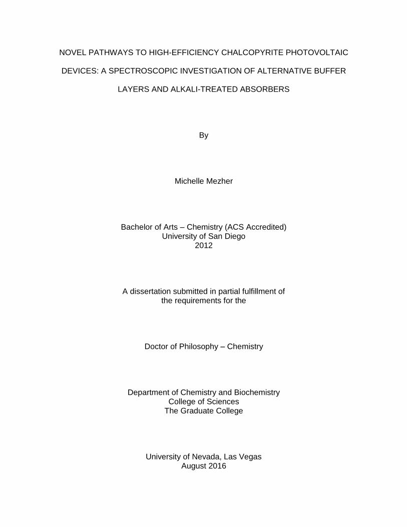
core levels into the vacuum. Their kinetic energy (KE) can be measured, offering chemical
state information, predominantly of the sample surface due to the short inelastic mean
free paths (IMFP) of the emitted photoelectrons78. A schematic of the XPS process is
displayed in Figure 3.1. The transition causes the system to be in a core-ionized state,
and energy conservation dictates that
20
hv = KE + |BE| (3.2)
with BE representing the binding energy and KE includes the work function, Φsample, of
the sample. The energies are relative to the Fermi energy (EF), achieved by grounding
the sample to the detector and calibrating the energy axis following ISO standards
proposed by Seah80. XPS is powerful in terms of determining chemical environments due
to the BE of the photoelectrons serving as a “fingerprint” of the photoelectron in question.
Shifts in the BE also gives information on bonding environments, oxidation states, and
adsorbate presence, as well as final state effects, such as (variations in) screening of the
Figure 3.1: Schematic of a) X-ray photoelectron spectroscopy (XPS) and b) X-ray
Auger electron spectroscopy (XAES) transitions.

21
hole(s) left behind in the final state. XPS spectra are usually plotted as intensity (count
rate) vs. BE, since the KE of the photoelectron is dependent on the excitation energy.
3.2.2 – X-ray-excited Auger Electron Spectroscopy (XAES)
X-ray Auger electron spectroscopy (XAES) is a secondary radiationless process that
takes place after a core-level is ionized. Figure 3.1 presents a schematic of this process.
For example, an electron in the K shell (1s core level) is ionized, leaving behind a hole
allowing an electron from an outer level, L2 (2p1/2), to relax into the hole. The energy
gained can now be used to emit a characteristic photon (X-ray fluorescence) or to emit
another electron in the same shell or a more shallow level (for example L3 (2p3/2)), leading
to Auger electron emission. The resulting notation takes into account the shells involved
in the Auger process (e.g., O KL2L3 or O KL3L2). XAES is element-specific due to the
localization of the core level wavefunction initially involved and, like XPS, sensitive to
bonding environments, oxidation states, the presence of adsorbates, and final state
effects (in this case involving two core or valence holes). XAES spectra are plotted as
intensity (count rate) vs. KE, since the KE of the Auger emission is independent of the
excitation source.
3.2.3 – Ultra-violet Photoelectron Spectroscopy (UPS)
The dispersive nature of the valence band (VB) requires a suitable excitation energy to
maximize the spectral contribution of the orbital-specific derived bands. The ionization
cross-section is largest when the excitation energy is similar to the orbital energy and
thus, while XPS can be used to probe the valence band, ultra-violet photoelectron
spectroscopy (UPS) would provide more information on this region due to the high flux of
photons and narrow line-width of the radiation78. He I (21.22 eV) and He

22
II (40.8 eV) are the most commonly used irradiation sources, however other noble gases
like Neon are used as well. By using a UV source (i.e., He discharge lamp), a valence
electron is excited out of the system and detected by the analyzer, as seen in Figure 3.2
(a). Following Fermi’s golden rule, the spectrum is dictated by the transition probability of
the valence band electron being excited to a one-electron final state at or above the
vacuum level. The UPS spectra are plotted as intensity (count rate) vs. BE (relative to
EF), with the onset of the spectra describing the maximum energy in the VB. UPS spectra
are calibrated using the EF of clean Au foil.
Figure 3.2: Schematic of a) ultra-violet photoelectron spectroscopy (UPS), and b)
inverse photoemission spectroscopy (IPES).

23
3.2.4 – Inverse Photoemission Spectroscopy (IPES)
Inverse photoemission spectroscopy (IPES) is complimentary to XPS and UPS, yielding
information on the unoccupied density of states above the EF. A schematic of the process
is shown in Figure 3.2 (b). A low energy electron beam hits the surface of the sample with
energy Ei, allowing electrons to relax into unoccupied final states with energy Ef in the
conduction band (i.e., above EF for a semiconductor). This electron relaxation emits a
photon with an energy of Ei-Ef, which is, in our case, detected with a Geiger-Müller
detector. The detector combines a SrF2 window and an Ar:I2 gas filling, creating a
bandpass filter at ~9.5 eV by combining the absorption onset of SrF2 with the molecular
photoionization energy of Iodine81:
ℎ𝑣 + 𝐼2 → 𝐼2+ + 𝑒− . (3.3)
By keeping the detection energy of the photon constant and changing the incoming
electron energy range (8-16 eV), it is possible to measure the intensity distribution of the
photons as a function of the final state energy (alternatively, it is possible to vary the
detected photon energy by using a monochromator-based detection system instead of
the band pass filter). The intensity distribution reflects the availability of empty electronic
states above the Fermi level. Similar to UPS, the IPES spectra are plotted as intensity
(count rate) vs. BE (relative to EF), with the onset of the spectra representing the minimum
energy in the conduction band (CB). The spectra are calibrated using the EF of a clean
Au foil.
3.2.5 – Combining UPS and IPES
Because UPS probes the VB and IPES probes the CB, the valence band maximum (VBM)
and conduction band minimum (CBM) can be determined. This forms the basis of band

24
offset evaluations, and can also result in experimentally derived electronic surface
bandgaps. In our group, a linear extrapolation is used to determine the VBM and CBM,
which has proven in the past to be effective in taking experimental broadening, final state
screening, inelastic losses, and dispersion of bands in k-space into
account15,23,25,51,53,59,60,82–86. Experimental broadening is, of course, present in both UPS
and IPES, and thus the linear extrapolation needs to account for a broadening-induced
tail. The tail depends on resolution and is a bigger issue for IPES spectra due to a poorer
resolution (~0.4 eV compared to ~0.2 eV for UPS). Inelastic losses and final state
screening can reduce the KE of the emitted electron, increasing the spectral intensity
below the “true” VBM (and above the “true” CBM). In k-space, the energy of the bands
depends on the crystal momentum of the electron, and hence the “true”, k-resolved VBM
and CBM will be an upper (lower) bound of the distribution of the corresponding band,
best described by a linear extrapolation.
3.2.6 – Surface Sensitivity
For XPS, UPS, XAES, and IPES, it is not the method of excitation that determines the
surface sensitivity of the measurements, but rather the inelastic mean free path (IMFP)
of the emitted (or incident) electrons. The longer the path of the electrons in the sample,
the more likely they will inelastically scatter, and the IMFP is furthermore dependent on
the kinetic energy of the electron and the sample composition (matrix). Inelastic scattering
originates from many mechanisms, including electron-electron interactions, electron-
photon interactions, electron-composition impurity interactions, etc87. After the inelastic
scattering process occurs, the scattered electrons might still reach the detector, but they
do not contribute to the intensity at the correct final state energy for

25
the transition described by Fermi’s golden rule. Instead, they contribute to the background
of the spectrum78. This also holds true for IPES, where the primary detection of photons
will come from electrons that have not lost energy prior to the radiation, while the
background arises from photons emitted from electrons that are inelastically scattered87.
Thus, the surface sensitivity of XPS, UPS, XAES, and IPES greatly depends on the IMFPs
of the electrons emitted from (relaxing into) the system. Figure 3.3 presents the “universal
curve” which shows the relationship between IMFP (λ) and the KE of the
photoelectron88,89. The IMFP of an electron is at a minimum around a KE of 20-30 eV and
Figure 3.3: The “Universal Curve” (line that averages the experimental data points)
presents the relationship of the inelastic mean free path of electrons as a function of
their kinetic energy relative to the vacuum level. Adapted from reference 88.
λ (
mo
no
layers
)
Electron Kinetic Energy (eV)

26
increases with a linear trend approximately √𝐾𝐸. The probability an electron travelling a
distance, d, through the solid without undergoing scattering:
𝑃(𝑑) = 𝑒−𝑑
𝜆 (3.3)
Thus, it is an exponentially surface-weighted signal.
3.2.7 – Peak Fitting
In XPS, characteristic peaks of different orbitals can overlap (for example, Ga 3d at 20
eV and In 4d at 18 eV), often convoluting the information that could be derived from said
peaks. Sophisticated software programs like FITYK90 allow the user to fit a spectrum
using various functions and create a model or fit (with a particular set of parameters) that
is in close agreement with the data. However, shake off or shake up satellite peaks,
multiplet splitting, etc., can cause features to appear in the spectrum that complicate fitting
the background and the “true” contributions to the peak intensity of the specific element’s
subshell.
Two popular methods to fit the background in an XPS spectrum include the
simultaneous subtraction of a linear background (generally best for semiconductors) or,
for metals, the prior removal of a Shirley background91,92 (possibly combined with the
subtraction of an additional linear background/correction function as a simultaneous
contribution during the fit). To describe the peak(s) in an XPS spectrum, symmetric Voigt
functions are most appropriate for semiconductors (all fits performed in this dissertation
use symmetric Voigt functions), as the function replicates contributions from both
Gaussian and Lorentzian broadening. The Gaussian broadening, to first approximation,
is intended to describe the experimental broadening, while the Lorentzian portion
describes lifetime broadening of the core-hole. Metal XPS peaks are generally best

27
described by asymmetric line shapes, either an asymmetric Voigt or a Doniach-Ŝunjić line
profile93. Among other parameters, fitting the peak requires taking spin-orbit splitting and
appropriately coupled values for Gaussian and Lorentzian line width contributions into
account. The resulting residual (i.e., the difference between experimental data and fit)
offers a function of merit for the fit.
3.3 – SAMPLE PREPARATION AND MEASUREMENT PARAMETERS Ultra-high vacuum (UHV) is required to detect the electrons (photons for IPES) emitted
from (or directed at) the sample to minimize collisions with gas particles between the
sample and detector. In our group, samples are stored and prepared for measurement in
an inert atmosphere environment (N2) glovebox to minimize the amount of surface
adsorbates. Once a sample is mounted onto a sample holder and electrically connected,
it is introduced into the UHV system through a load-lock without any air exposure. XPS
measurements are taken using Mg Kα (1253.6 eV; 1s → 2p transition) and Al Kα (1486.6
eV; 1s → 2p transition) radiation, and He I (21.22 eV; 1s2 → 1s2p transition) and He II
(40.81 eV; 1s → 2p transition) irradiation are used for the UPS measurements. For this
dissertation , XPS and UPS measurements were taken with a SPECS PHOIBOS 150
MCD electron analyzer (fixed analyzer transmission mode), calibrated using core-level
and Auger peaks of clean Ag, Cu, and Au foils (for XPS)78, and the EF of the Au foil (for
UPS and IPES). A commercial low-energy electron gun (Staib) and a custom-built Dose-
type detector with a SrF2 window and Ar:I2 filling81 were used for IPES experiments. The
base pressure in the chamber was better than 5×10⁻¹⁰ mbar.
Because XPS and UPS are very surface sensitive, special care (the collaborators
are asked to do the same) was taken to avoid any air exposure. Since the purpose of

28
XPS, UPS, and IPES is to derive the surface electronic and chemical structure of the
relevant surface/interface, surface adsorbates not only attenuate the pertinent peaks of
the sample, but can also cause surface oxidation rendering the surface “not relevant”. To
reduce the amount of surface adsorbates, samples were treated with a low-energy (50
eV) Ar+ ion treatment at a low incidence angle, which has shown to be very effective in
removing adsorbate (C and O) contaminants from CdS, ZnO, and chalcopyrite surfaces
without creating metallic phases25,83. An example illustrating ion treatments reducing
surface adsorbates is shown in Figure 3.4 and 3.5. XPS measurements show surface
contamination of C and O adsorbates on the bare CIGSe absorber, most notable by
analyzing the C KVV, O 1s, and O KLL peaks (note the Ga LMM peaks overlap with the
1000 800 600 400 200 0
Inte
nsity (
a.u
.)
Binding Energy (eV)
O 1s
In 3d
In 3p
O K
LL
In 3s
In M
NN
Cu 2p
C K
VV
XPS Mg KSurvey
CIGSe Bare Absorber
Ga 2p
Na 1s
120 min
0 min
60 min
Treatment Time
Figure 3.4: Mg Kα survey spectra of the Cu(In0.7,Ga0.3)Se2 absorber as a function of
treatment time during a low-energy ion cleaning series. Spectra in the blue box are
shown on an enlarged energy axis in Fig. 3.5.

29
C 1s). The pertinent CIGSe photoemission and Auger lines (Cu, In, Ga, Se), as well as
the Na lines are labeled, in addition to the adsorbate peaks associated with C and O. Two
subsequent surface cleaning steps (of 60 minutes each) were taken in order to remove
or reduce these adsorbate peaks. Due to the surface sensitivity of PES measurements,
the C and O peaks are particularly pronounced since these atoms are located on the
external surface. Consequently, all low-kinetic energy peaks (e.g., Ga 2p, Cu 2p, In MNN)
are suppressed in intensity. Comparing the survey spectra taken after each ion treatment,
the signal intensity of the CIGSe peaks are less attenuated, especially those at the higher
BE region (lower KE), as the adsorbate peaks decrease. The Na 1s and Na KLL peaks
also decrease with each treatment. Detailed spectra offer a better view of peak shifts with
400 350 300 250 200 150 100 50 0
120 min
Inte
nsity (
a.u
.)
Binding Energy (eV)
XPS Mg KSurvey
CIGSe Bare Absorber
Na 2p
Na 2s
Na KLL
Se 3s
Cu 3
s/I
n 4
s
Cu 3
p/I
n 4
p
Cu LMM
C 1s
In 4
d/G
a 3
d
Cu 3d
Se 3d
Ga 3p
Se 3p
Ga 3s
Ga L
MM
0 min
60 min
Treatment Time
Figures 3.5: XPS spectra of the low binding energy region before and after two low-energy ion treatment steps.

30
the ion treatments. The band gap offset is determined by looking at relative core level
peak shifts for the different layers. An adsorbate layer on the surface can cause the core
level peaks to shift and hence found at peak position not representative of the “true”
surface, but of the adsorbate contributions to the surface. For the untreated sample, the
valence and the conduction band are dominated by the adsorbate contribution and thus
shows a larger band gap, as seen in the UPS and IPES spectra in Figure 3.6. However,
with each ion treatment, the Cu 3d-derived peak at ~ 3eV becomes more pronounced
and the valence band and conduction band exhibit reduced values which are closer to
-6 -4 -2 0 2 4 6
+/- 0.15 eV
Treatment
Time
120 min
No
rmaliz
ed Inte
nsity
Binding Energy rel. EF (eV)
60 min
1.96 eV
IPESUPS He I
CIGSe
1.57 eV
0 min
1.27 eV
+/- 0.10 eV
Figure 3.6: UPS and IPES spectra, showing the band edge positions (VBM and CBM)
as well as the electronic surface band gap of the CIGSe absorber as a function of
treatment time.

31
previously reported values25,51,52,59,60,84,86. Note that the error bars of the techniques are
not “statistically derived”. They describe a range of probabilities.
3.4 – SYNCHROTRON-BASED SOFT X-RAY SPECTROSCOPY 3.4.1 – X-ray Emission Spectroscopy (XES)
X-ray emission spectroscopy (XES) is a photon in – photon out spectroscopy technique
in which a core-hole is filled by an electron from the valence band (as a “0th step”, a photon
has previously excited a core electron and removed it from the system). The XES
transition emits a photon with an energy given by the energy difference between the levels
Figure 3.7: Schematic of x-ray emission spectroscopy transitions. The “zero” step of
the process is colored gray while the XES process is in red.

32
involved in the transition. A schematic of the XES process is shown in Figure 3.7. The “0th
step” of the process is shown in gray, while red represents the XES process. Possible
presence of core-exciton states can be distinct and discernable in a spectrum and often
appear as additional states near the VBM (XES) or CBM (x-ray absorbance
spectroscopy)94. As a result, the core-exciton obscures the true VBM (CBM) and resulting
bandgap approximations should be taken as a minimum value23. The XES process is
governed by the dipole selection rule (Δl = ± 1), resulting in a spectrum where only suitable
valence states will be observed. XES thus represents a measurement of the partial
occupied density of states near the probed atom (i.e., the near the original core hole).
This is in contrast to XPS and XAES, which measure the total occupied density of states.
Similar to PES, the intensity of the emitted photons in the XES process also follows
Figure 3.8: The fluorescence and Auger yields for the K subshell as a function of
Atomic number Ref. from 96, 97.

33
Fermi’s Golden rule (see equation 3.1). While the surface sensitivity of PES is governed
by the IMFP of the emitted electrons, XES is governed by the attenuation lengths of the
involved photons95. Depending on the excitation energy for a XES measurement, the
near-bulk to bulk region is probed, in contrast to the surface-sensitive measurements of
PES. The x-ray emission process is in competition with the Auger emission process.
Figure 3.8 displays the fluorescence and Auger yields for the K subshell as a function of
atomic number96,97. The Auger emission dominates for low atomic numbers, causing the
probability of radiative decay in the soft x-ray regime to be very low96,98. Only for higher
atomic numbers does the fluorescence become comparable (and, eventually, dominant)
to the Auger yield. At these atomic numbers, the emitted fluorescence photon will have
energies in the hard x-ray regime and offer substantially reduced chemical information.
To nevertheless also gain insights in the chemical bonding and occupied valence
states with soft x-ray XES, it is possible to overcome the “yield challenge” by utilizing a
high flux, tunable excitation source and a high-efficiency spectrometer (as will be
described in the following section). This allows for measurement times comparable to lab-
based techniques like XPS and XAES.
3.4.2 – Beamline Description
XES experiments were performed on Beamline 8.0.1.1 at the Advanced Light Source
(ALS), Lawrence Berkeley National Laboratory. Figure 3.9 offers a look at the set-up of
Beamline 8.0.199. The synchrotron radiation is produced by a 5-cm period undulator (and
used in the first, third, or fifth harmonic). The beamline allows an energy range of 80-1250
eV and a photon flux between 1011 and 6x10¹⁵ photons per second, depending on the
resolution and energy99. Apertures and focusing mirrors shape and direct the beam

34
through the entrance slit, monochromator spherical grating, and exit slit. The beam can
be directed to either the permanently installed Soft X-ray Fluorescence (SXF)
endstation100 or the custom-built Solid and Liquid Spectroscopic Analysis (SALSA)
endstation101. SALSA utilizes a high-efficiency variable line spacing (VLS) spectrometer,
which has a spectral resolving power of E/ΔE > 1200 over the energy range 120 to 650
eV. The SXF spectrometer is based on the Rowland Circle concept and has a spectral
resolving power E/ΔE between 400 and 1900102. XES data in this dissertation were taken
on either the SALSA or SXF endstation, which will be noted in the experimental section
of each chapter.
Figure 3.9: Schematic of Beamline 8.0.1 at the Advanced Light Source (ALS). Taken from ref. 99

35
CHAPTER FOUR
CHEMICAL AND ELECTRONIC SURFACE PROPERTIES OF ALKALI-TREATED
CIG(S)Se ABSORBERS: COMPARISON OF INDUSTRY AND NATIONAL LAB THIN-
FILM CHALCOPYRITE ABSORBERS
4.1 – INTRODUCTION In November 2014, a new world record efficiency for CIGSe thin-film photovoltaics with a
flexible substrate was set by EMPA, raising the efficiency from 18.7% to 20.4%10. At this
time, NREL held the world record, 20%, for CIGSe deposited on a soda-lime glass
substrate, and today’s chalcopyrite world record is 22.3 %, achieved with Zn-based buffer
layer, CIGSSe absorber, and a soda lime glass substrate by Solar Frontier4,54,103). The
reason for the large jump in conversion efficiency was attributed to alkali-post deposition
treatments (PDT) which arguably, changed interfacial properties between CIGSe and
CdS along with mitigating optical losses in the CdS buffer layer10. With this new record,
KF treatments became the new “hot topic” in the chalcopyrite industry and only a year
after the 20.4% record was set, ZSW achieved a new world record of 21.7%104 (on a soda
lime glass substrate). While the importance of Na incorporation into the CIGSe absorber
is well known and established35–38, research into the effect of KF have only emerged in
the past few years.
A common finding with the KF-PDT is the depletion of Cu on the surface of the
CIGSe, which in turn affects the surface electronic structure; however, this has only been
reported for CIGSe deposited using the three-stage coevaporation process commonly
used to create laboratory-scale research devices 10,34,43. Industrial companies, on the
other hand, often incorporate S into the chalcopyrite absorber and do not use the three-

36
stage coevaporation process, instead opting for cheaper and streamlined deposition
processes on both rigid and flexible substrates 105–107. Because there is a need to bridge
the gap between laboratory scale and industrial module efficiencies, more research is
required in order to understand the role of KF in industry made chalcopyrites and its
comparison to laboratory scale results.
Thus, to gain insight on the effects of KF PDTs on industry deposited CIGSSe and
compare them to laboratory scale CIGSe, we employ XPS and UPS (at UNLV), as well
as XES (at the ALS) to investigate the chemical and electronic properties of the absorbers
surface.
4.2 – EXPERIMENTAL DETAILS Two alkali-PDT CIG(S)Se sample series were deposited, one at NREL and one at STION
utilizing two different absorber deposition techniques. The NREL PDIL (process
development and integration laboratory) CIGSe absorbers were deposited using the
standard three-stage process (Ga/(Ga+In) = 0.3) on a Mo-sputtered soda lime glass
substrate 18. The deposition of the STION CIGSSe absorbers utilized a proprietary 2-
stage sputter process. The first step involves physical vapor deposition of Cu, In, and Ga
while the second step involves the sulfurization and selenization of the metals to create
the CIGSSe semiconductor. Note that the STION absorbers contain S while the NREL
PDIL absorbers do not. The alkali (Na and K) post-deposition treatments were performed
at NREL for both the STION and NREL PDIL absorbers resulting in two sample sets of a
bare absorber, NaF-PDT absorber and two KF-PDT absorbers. All samples, excluding
the bare absorbers, were rinsed (100 ml H2O + 12.5 mL 28% NH4OH reagent) for four
minutes at 65 C. The samples each gave different device efficiencies with the NREL NaF-

37
treated absorber having the highest efficiency (18.2%) and one of the NREL PDIL KF-
treated absorbers having the least (2.8%). The absorbers identification is presented as
following: STION CIGSSe absorbers: “Bare-14.6%”, “NaF-14.6%”, “KF-4.5%”, and “KF-
11%”. NREL CIGSe absorbers: “Bare-17.9%”, “NaF-18.2%”, KF-2.8%”, and “KF-16.7%”.
The numbers correspond to the efficiency of that particular sample.
The samples were briefly air-exposed, packed and vacuum-sealed under dry
nitrogen before being sent to UNLV. The samples were unsealed in an inert environment,
mounted, and introduced to the UHV system. XPS, UPS (UNLV), and XES (ALS) were
utilized to investigate the chemical and electronic structure of both the STION and NREL
sample sets. Mg Kα and Al Kα irradiation and a SPECS PHOIBOS 150 MCD electron
analyzer were employed for XPS measurements and He II for the UPS measurements.
The spectra were calibrated using Auger and core-level peaks of clean Cu, Ag, and Au
foils (XPS) 80 and the Fermi energy of a clean Au foil (UPS).
X-ray emission spectroscopy was conducted at beamline 8.0.1 in the ALS utilizing
a high-transmission variable-line grating spectrometer (VLS) on the SALSA endstation101
for the S L2,3 edge. The K L2,3 and F Kα were taken on the soft x-ray fluorescence (SXF)
endstation100 installed on beamline 8.0.1 and calibrated according to the appropriate
references (CdS108 for the S L2,3 and KF for K L2,3 and F Kα).
All peaks were analyzed by fitting the different spectral intensities with Voigt
functions (with coupled Lorentzian and Gaussian widths) and a linear background using
the Fityk peak-fitting program90. The valence band maximum (VBM) was determined by
linear extrapolation of the leading edge in the valence band (UPS) spectra109. The base

38
pressure in the UNLV analysis chamber, VLS analysis chamber, and SXF chamber were
<5×10⁻¹⁰ mbar, <1×10⁻⁹ mbar, and <1×10⁻⁹ mbar, respectively.
4.3 – RESULTS AND DISCUSSION
The XPS survey spectra of the CIG(S)Se absorbers normalized to the In 3d5/2 peak area
(to look at respective Cu:In, Ga:In, and Se:In ratios) are presented in Figure 4.1. All the
pertinent CIG(S)Se peaks are present and labeled (i.e. Cu, Ga, Se, In, S) along with
peaks associated with Na and surface adsorbates (C and O). The STION annealed
absorber has an unusually high O 1s and O KLL peaks in comparison to the much smaller
O signal seen for all other samples while the C 1s and C KVV peaks are similar among
all the samples. Substantial Na 1s and Na KLL peaks are present for both the STION and
1200 1000 800 600 400 200 0
S L
MM
Inte
nsity N
orm
aliz
ed
to In
5/2
pe
ak a
rea
Binding Energy (eV)
XPS Mg K Survey
STION Bare-14.6%
(annealed)
NREL Bare-17.9%
STION NaF-14.6%
NREL NaF-18.2%
STION KF-4.5%
NREL KF-2.8%
STION KF-11%
NREL KF-16.7%
Na KLL
Se 3s
S 2s
Cu 3
s/I
n 4
s
Cu 3
p/I
n 4
p
Cu LMM
C 1s
In 4
d/G
a 3
d
Se 3d
Ga 3p
Se 3p
Ga 3s
S 2p
Ga
LM
M
CIG(S)Se
B 1s
O 1s
In 3d
In 3p
O K
LL
In 3s
In M
NN
Cu 2p
C K
VV
Ga 2p
Na 1
s
Figure 4.1: XPS survey spectra normalized to the In5/2 peak area of the NREL and STION bare absorbers (black), both NaF-treated absorbers (red), both low efficiency KF-treated absorbers (blue), and both high efficiency KF-treated absorbers (pink).

39
NREL bare absorber and small Na peaks are seen for the NREL NaF rinsed sample. The
Na peaks for the other samples are either not present or too small to view at the scale of
the survey spectra. They will be discussed in more detail later. Because the survey
spectra are normalized to the In 3d5/2 area, changes in the Cu:In ratio are clearly seen
between the rinsed samples with the low efficiency KF-rinsed samples have the largest
Cu intensities, indicating a more Cu-rich surface. The Ga signal is very weak for all the
STION absorbers, suggesting a more Ga-poor surface in comparison to the NREL
absorbers. The STION bare absorber has an additional peak at 193 eV, which is most
likely B 1s (which will be discussed in detail). While analyzing survey spectra allows for
an overview of what is occurring on the sample surfaces, detailed regions of the various
core-level and Auger peaks allow for a more in depth analysis of the surfaces.
Thus, in order to gain insight on the Cu:In ratio changes between the samples, the
Cu 2p3/2 peak in Figure 4.2 (left) is normalized to the In 3d5/2 area. Both low-efficiency KF
samples have the most Cu-rich surface in the sample series, with the amount of Cu being
comparable between the two samples. In general, the STION absorbers exhibit a more
Cu-rich surface relative to the NREL absorbers. It is well known in the CIGSe community
that a Cu-poor surface for the CIGSe absorbers helps lead to higher efficiency
devices21,24,110. Note also that while the Cu:In ratio decreases with alkali-treatment (KF-
2.8% is the exception) for the NREL absorbers, the opposite is seen for the STION
absorbers. In fact, the Cu:In ratio is almost doubled for the KF-11% absorber, suggesting
that although both set of absorbers received the same KF-PDT, the industry absorbers
do not have the same Cu depletion at the surface that has been published for research-
based laboratory scaled absorbers10,34,43. In Figure 4.2 (right), the Cu 2p peaks are

40
normalized to the main peak height in order to look at shape changes between the
spectra. The component seen at ~957 eV is indicative of Cu-O bonds and it is present in
all the samples except the low-efficiency KF-treated absorbers. The Cu 2p peaks of all
the rinsed samples shift towards lower binding energies relative to the bare absorber of
the respective sets.
The Ga intensity relative to In is investigated in Figure 4.3, left, while the shape
changes of the peak are seen on the right. In general, the STION absorbers exhibit a
more Ga-poor surface relative to the NREL absorbers. Both high-efficiency KF absorbers
exhibit the lowest Ga:In ratio indicating the surface of these absorbers are more Ga-poor
938 936 934 932 930 928
No
rma
lize
d t
o I
n 3
d5/2 A
rea
Binding Energy (eV)
Bare-14.6%
NaF-14.6%
KF-4.5%
KF-11%
STION
NRELBare-17.9%
NaF-18.2%
KF-2.8%
KF-16.7%
XPS Mg K
Cu 2p3/2
965 960 955 950 945 940 935 930 925
Bare-14.6%
NaF-14.6%
KF-4.5%
KF-11%
Binding Energy (eV)
XPS Mg K
Cu 2p
STION
NRELBare-17.9%
NaF-18.2%
KF-2.8%
KF-16.7%
Cu-O
No
rma
lize
d I
nte
nsity
Figure 4.2: XPS detailed spectra of the Cu 2p3/2 peak normalized to the In5/2 peak area
(left) and to Cu 2p3/2 peak height (right) of the NREL and STION bare absorbers (black),
NaF-treated absorbers (red), and low and high efficiency KF-treated absorbers (blue,
pink).

41
than the respective samples in their set. The NREL bare absorber Ga 2p3/2 peak is
asymmetrical suggesting the presence of multiple Ga species. All the rinsed samples
shift ~0.6 eV towards lower binding energies relative to their respective bare absorbers.
This could signal a change in chemical environment (removal/reduction of Ga-O) and/or
band bending at the surface.
To confirm that Ga-O species are present, the Ga LMM peak needs to be analyzed,
as seen in Figure 4.4 (left). A third component, indicative of a Ga-O species, is visible for
the NREL bare absorber at ~1063 eV (kinetic energy). It is more difficult to assess if this
peak is found on the STION bare absorber due to the additional peak, not associated with
1122 1120 1118 1116 1114
No
rmaliz
ed Inte
nsity to In 3
d5/2 A
rea
Binding Energy (eV)
Bare-14.6%
NaF-14.6%
KF-4.5%
KF-11%
XPS Mg K
Ga 2p3/2
STION
NRELBare-17.9%
NaF-18.2%
KF-2.8%
KF-16.7%
1122 1120 1118 1116 1114
No
rma
lize
d I
nte
nsity
Binding Energy (eV)
Bare-14.6%
NaF-14.6%
KF-4.5%
KF-11%
XPS Mg K
Ga 2p3/2
STION
NRELBare-17.9%
NaF-18.2%
KF-2.8%
KF-16.7%
Figure 4.3: XPS detailed spectra of the Ga 2p3/2 peak normalized to the In5/2 peak area
(left) and to Ga 2p3/2 peak height (right) of the NREL and STION bare absorbers
(black), NaF-treated absorbers (red), and low and high efficiency KF-treated absorbers
(blue, pink).

42
Ga LMM, at ~1060 eV. By rinsing the absorbers with an alkali-treatment, the Ga-O
contaminant species was removed and/or reduced. A small shoulder is visible for both
NaF absorbers indicating that the rinse did not completely remove the Ga-O species while
for all the KF species, the shoulder is not detected. Further analyzing the STION bare
absorber shows that the large peak at ~1060 eV is not actually part of the Ga LMM profile
and this is proven by switching excitation sources and measuring the same region.
In the top of Figure 4.4 (right), the NREL bare absorber Se LMM Auger region
taken with Al Kα is shown in blue and underneath, in black, is the same region taken Al
Kα of the STION bare absorber. The energy axis of this graph is now in binding energy
1055 1060 1065 1070 1075 1080
Inte
nsity N
orm
aliz
ed
to
In
3d
5/2
Are
a
Kinetic Energy (eV)
XPS Mg K
Ga LMM
Bare-14.6%
NaF-14.6%
KF-4.5%
KF-11%
STION
NRELBare-17.9%
NaF-18.2%
KF-2.8%
KF-16.7%
B 1s
200 195 190 185 180 175
Mg K Detailed
Al K Survey
STION bare
absorber
Binding Energy (eV)
Ga LMM
XPS Mg KAl K
Al K Survey
NREL bare absorber
STION bare
absorber
Se LMM
B 1s
Figure 4.4: XPS detailed spectra of the Ga LMM Auger peak normalized to the In 3d5/2
peak area (left) and to Ga LMM peak height (right) of the NREL and STION bare
absorbers (black), NaF-treated absorbers (red), and low and high efficiency KF-treated
absorbers (blue, pink).

43
(whereas the left graph is kinetic energy). With different excitation energies, the binding
energy of the Auger peak will change (the kinetic energy, however, will not). Thus, the
red spectrum is the same region but taken with Mg Kα excitation. This is why the Se LMM
appears in the Al Kα spectrum (but not the Ga LMM) and the Ga LMM appears in the Mg
Kα spectrum (but not the Al Kα spectrum) in this region. Using the dotted line as a guide
for the eye, there appears to be a component in the black spectrum (Al Kα) that is in the
same position as the peak in the red spectrum below. However, to make sure that this
component was not a part of the Se LMM profile, the Se LMM of the NREL bare CIGSe
absorber is featured above (blue) and it is clear that this component is not part of the Se
LMM. Thus, it is not part of the Ga LMM as well. This peak at 193 eV (1060 eV kinetic
energy) is attributed to B 1s, corroborated by literature 111,112 and suggests a B
contamination in the production line of the STION bare absorber. Note, this peak is not
found in the XPS spectra of the other samples.
In order to take a closer look at the surface Ga/(Ga+In) ratio, fits of the Ga 3d/In
4d region were created and are presented in Figure 4.5 (NREL) and Figure 4.6 (STION).
All the peaks were fit with a linear background, Voigt functions and couple Gaussian and
Lorentzian contributions. The spin-orbit splitting and the spacing between the In 4d5/2 and
In 4d3/2 and in between the Ga 3d5/2 and Ga 3d3/2 were fixed (0.86 eV for In and 0.46 eV
for Ga) according to literature113–115. The resulting residual of the fit is shown below each
region in purple (note the magnification factors). These shallow core levels already
possess some band character, and thus the quality of the fit is very surprisingly high for
the NREL absorbers, especially given all the above-mentioned boundary conditions
included in the fit. It is apparent that the surface Ga/(Ga+In) ratio changes with the alkali-

44
16171819202122
± 0.1
Ga 3d3/2
Ga 3d5/2
In 4d3/2
Binding Energy (eV)
x5
XPS Mg K
Ga 3d / In 4d
In 4d5/2
NREL Bare-17.9% Ga
Ga+In: 0.41
16171819202122
± 0.1
Binding Energy (eV)
x5
XPS Mg K
Ga 3d / In 4d
NREL NaF-18.2%
Ga
Ga+In: 0.31
16171819202122
± 0.1
Binding Energy (eV)
x5
XPS Mg K
Ga 3d / In 4d
NREL KF-2.8%
Ga
Ga+In: 0.36
16171819202122
± 0.1
Binding Energy (eV)
x6
XPS Mg K
Ga 3d / In 4d
NREL KF-16.7%
Ga
Ga+In: 0.26
Figure 4.5: XPS detailed spectra of the Ga 3d / In 4d region of the NREL bare absorber
(top left), NaF-treated absorber (top right), and low and high efficiency KF-treated
absorbers (bottom left and right).

45
21 20 19 18 17 16
± 0.1
Binding Energy (eV)
Ga 3d3/2
Ga 3d5/2
In 4d3/2
x3
XPS Mg K
Ga 3d / In 4d
In 4d5/2
STION Bare-14.6%
Ga
Ga+In: 0.11
21 20 19 18 17 16
Binding Energy (eV)
x3
XPS Mg K
Ga 3d / In 4dSTION NaF - 14.6%
Ga
Ga+In: 0.09 ± 0.1
21 20 19 18 17 16
± 0.1
Binding Energy (eV)
x3
XPS Mg K
Ga 3d / In 4dSTION KF - 4.5%
Ga
Ga+In: 0.06
21 20 19 18 17 16
± 0.1
Binding Energy (eV)
x3
XPS Mg K
Ga 3d / In 4dSTION KF - 11%
Ga
Ga+In: 0.09
Figure 4.6: XPS detailed spectra of the Ga 3d / In 4d region of the STION bare absorber
(top left), NaF-treated absorber (top right), and low and high efficiency KF-treated
absorbers (bottom left and right).

46
treatments for the NREL absorbers. The NREL bare absorber has a Ga/(Ga+In) of 0.41
± 0.10 eV. Visually, it is apparent there is more Ga at the surface due to the shoulder at
~20 eV being larger than the shoulder seen for the other NREL absorbers. The high
efficiency KF-treated NREL absorber has the lowest Ga/(Ga+In), 0.26 ± 0.10 eV, and the
low efficiency KF-treated NREL absorber has the largest Ga/(Ga+In) ratio (among the
rinsed absorbers), 0.36 ± 0.10 eV. The Ga/(Ga+In) of the NaF-treated NREL absorber is
0.31 ± 0.10 eV. There is less of a change in the Ga/(Ga+In) for the STION absorbers, as
seen in Figure 4.6. The fits themselves are also of a lower quality as seen in the residual
(note the magnification factors) due to the very small Ga content on the surface. The
addition of more components with the fixed boundary conditions did not further enhance
the residual. The STION bare absorber has a surface Ga/(Ga+In) ratio of 0.11 ± 0.10 eV
and the ratio for the treated STION absorbers do not really deviate from the bare absorber
ratio. Both the NaF and high efficiency KF-treated STION absorbers have a Ga/(Ga+In)
of 0.09 ± 0.10 eV and the low efficiency KF-treated absorber has a Ga/(Ga+In) of 0.06 ±
0.10 eV. While there is a larger difference in the Ga/(Ga+In) ratios of the treated NREL
absorbers in comparison to the untreated absorber, the Ga/(Ga+In) ratios for the STION
absorbers are essentially the same.
The Se 3d peak normalized to the In 3d5/2 peak area is shown in Figure 4.7, right,
while the Se 3s and S 2s are shown on the left. The STION absorbers exhibit a more Se-
poor surface relative to the NREL absorbers. Both the STION and NREL low efficiency
KF-treated absorbers have the highest Se:In ratio, i.e. the surface is more Se-rich. There
is a small component at ~ 59 eV present for the STION absorbers but not for the NREL
absorbers. This component is indicative of SeOx being present on the STION absorber

47
surfaces. Both NaF and high efficiency KF-treated absorbers shift toward lower binding
energy while both low efficiency KF-treated samples shift towards higher binding
energies. On the right of the figure, the Se 3s and S 2s peaks are normalized to the Se
3s of the respective sample sets. This normalization allows variations in the S:Se ratio in
the STION samples (no S is expected in the NREL absorbers) to be seen along with shifts
in the peaks. The peak shifts seen for the Se 3s follow the same pattern as discussed
above for the Se 3d. The S:Se ratio for the STION absorbers clearly change as a function
of alkali-treatment. The lowest S:Se ratio is seen for the low efficiency KF-treated sample
60 58 56 54 52 50
No
rma
lize
d I
nte
nsity to
In
3d
5/2 A
rea
Binding Energy (eV)
Bare-14.6%
NaF-14.6%
KF-4.5%
KF-11%
STION
NRELBare-17.9%
NaF-18.2%
KF-2.8%
KF-16.7%
XPS Mg K
Se 3d
236 234 232 230 228 226 224
Binding Energy (eV)
Bare-14.6%
NaF-14.6%
KF-4.5%
KF-11%
STION
NRELBare-17.9%
NaF-18.2%
KF-2.8%
KF-16.7%
XPS Mg K
Se 3s / S 2s
Se 3s
S 2s
No
rmaliz
ed Inte
nsity to S
e 3
s P
eak H
eig
ht
Figure 4.7: XPS detailed spectra of the Se 3d peak normalized to the In 3d5/2 peak
area (left) and to Se 3s peak height (right) of the NREL and STION bare absorbers
(black), NaF-treated absorbers (red), and low and high efficiency KF-treated absorbers
(blue, pink). The S 2s peak intensity for the STION absorbers changes as a function of
alkali-treatment.
48
and the highest is seen for the bare absorber. The NaF-treated absorber has a higher
S:Se ratio than the high efficiency KF-treated sample. The spectra indicate that alkali-
treatments of sulfur-containing chalcopyrites inherently changes the surface S:Se ratio.
Detailed spectra, normalized to peak height, of the In 3d5/2 (left) and the In MNN
(right) are presented in Figure 4.8. The alkali-rinsing for both the STION and NREL
samples shifts the In peak towards lower BE with the STION KF-4.5% and NREL NaF-
18.2% samples shifted the most. The shift suggests a reduction of an In-oxide species.
The STION bare absorber is shifted 0.20 eV towards lower BE relative to the NREL bare
absorber suggesting the STION bare absorber contains less surface In-oxide species
449 448 447 446 445 444 443 442 441
No
rma
lize
d I
nte
nsity
Binding Energy (eV)
Bare-14.6%
NaF-14.6%
KF-4.5%
KF-11%
STION
NRELBare-17.9%
NaF-18.2%
KF-2.8%
KF-16.7%
XPS Mg K
In 3d5/2
395 400 405 410 415
Kinetic Energy (eV)
Bare-14.6%
NaF-14.6%
KF-4.5%
KF-11%
STION
NRELBare-17.9%
NaF-18.2%
KF-2.8%
KF-16.7%
XPS Mg K
In MNN
Figure 4.8: XPS detailed spectra of the In 3d5/2 peak (left) and the In MNN (right)
normalized to peak height of the NREL and STION bare absorbers (black), NaF-treated
absorbers (red), and low and high efficiency KF-treated absorbers (blue, pink).

49
than the NREL bare absorber. Analyzing the In MNN peak reveals that indeed, there is a
reduction of In-oxide with the alkali-treatments. The added intensity on the In MNN
shoulder at ~398 eV and the depth of the dip at ~405 eV shows this. The STION and
NREL absorbers exhibit the most shallow dip with the NREL absorber a bit more shallow.
With the alkali-treatment for both sets of samples, there is a reduction in the shoulder at
~398 eV, the dip at ~405 eV becomes deeper, and there is a reduction in the peak
broadening. While the NaF and high efficiency KF-treated samples have similar surface
In-oxidation, both low efficiency KF-treated samples have the least.
There has been some question as to whether K residue is left on the absorber
surface after a KF-treatment. In fact, it can be seen with both the NREL and STION
300 298 296 294 292 290 288
No
rma
lize
d I
nte
nsity
Binding Energy (eV)
Bare-14.6%
NaF-14.6%
KF-4.5%
KF-11%
STION
NRELBare-17.9%
NaF-18.2%
KF-2.8%
KF-16.7%
XPS Mg K
K 2p
change:0.40 eV
carbonates
300 298 296 294 292 290 288
change:0.16 eV
Binding Energy (eV)
Kmetallic
K-F
NRELBare-17.9%
NaF-18.2%
KF-2.8%
KF-16.7%
XPS Mg K
K 2p
change:0.40 eV
Figure 4.9: XPS detailed spectra of the K 2p peak (left). A closer look at the K 2p for
the NREL absorbers is shown at the right along with K references.

50
absorbers in Figure 4.9, that indeed there is K deposited on the surface of not only all the
KF-treated absorbers, but also the NaF and bare NREL absorbers. However, the K
residue concentration is different between the STION and NREL absorbers, with the
STION KF-treated absorbers having a significantly lower concentration of K on the
surface relative to the NREL absorbers. It has been reported for the EMPA record
absorber that the K deposited on the surface causes the Cu depletion10. While the data
for the NREL absorbers show a considerable amount of K deposited and Cu depletion on
the surface (except KF-2.8%), the data for the STION absorbers do not follow the same
trend. There are trace amounts of K on the surface and an increase in the Cu peak. Th
1080 1078 1076 1074 1072 1070 1068 1066
Inte
nsity N
orm
aliz
ed
to In 3
d5/2
Are
a
Binding Energy (eV)
Bare-14.6%
NaF-14.6%
KF-4.5%
KF-11%
XPS Mg K
Na 1s
STION
NRELBare-17.9%
NaF-18.2%
KF-2.8%
KF-16.7%
4.9 eV
540 538 536 534 532 530 528 526
Inte
nsity N
orm
aliz
ed
to
In
3d
5/2 A
rea
Binding Energy (eV)
Bare-14.6%
NaF-14.6%
KF-4.5%
KF-11%
STION
NRELBare-17.9%
NaF-18.2%
KF-2.8%
KF-16.7%
XPS Mg K
O 1s4.7 eV
Figure 4.10: XPS detailed spectra of the Na 1s (left) and O 1s peaks (right) normalized
to the In5/2 peak area of the NREL and STION bare absorbers (black), NaF-treated
absorbers (red), and low and high efficiency KF-treated absorbers (blue, pink).

51
e NREL high efficiency KF-treated absorber has the largest K signal and is shifted 0.4 eV
towards lower BE in comparison to the NREL bare absorber (right figure). Likewise, the
K 2p peaks are shifted 0.16 eV towards lower BE. Despite the shift, the BE of the K peaks
indicates a K-F bonding environment111.
Shifting attention to Na and O, Figure 4.10 (left) shows the presence of Na on all
four NREL absorbers as well as the STION bare and NaF-treated absorber. While both
the NREL and STION bare absorbers have the largest Na peaks in their respective sets,
the STION bare absorber has a larger Na 1s peak than the NREL bare absorber. The Na
peaks for both NaF absorbers shift toward lower BE. The O 1s peak (right) shows a
significantly high intensity for the STION bare absorber and amongst the rinsed samples,
both NaF absorbers exhibit the largest O 1s peak. As well, the O 1s peak of all the rinsed
samples are shifted towards lower BE, with both NaF-treated absorbers shifted the most.
The O 1s peak is broad and asymmetrical indicating multiple O species, including
hydroxides, which is not unexpected due to the nature of the KF and NaF PDT treatments.
Both low efficiency KF absorbers have an additional component at ~537 eV, indicative of
H2O111. The Na peak for the low efficiency NREL KF absorber exhibits a drastically
shifted Na peak (almost 5 eV) in both the core-level and Auger (not shown) spectra
indicating a different chemical species present. Although both the O and Na peaks for the
NREL low-efficiency KF absorber are shifted ~5 eV towards higher BE, the shifts are not
necessarily mutually exclusive, especially since the BE of the O 1s peaks indicates the
presence of H2O on the surface. In order to further investigate the chemical environment
of Na for all the absorbers, a modified Auger parameter plot was constructed116 and is
shown in Figure 4.11. A modified Auger parameter plot aids in identifying potential

52
species using both the Na KLL and Na 1s peak separation. All of the absorbers, except
NREL KF-2.8%, are clustered between the Auger parameters 2061 and 2063 along with
all of the Na-oxide species. It is clear that the Na on the absorbers are not metallic. The
NREL KF-2.8% absorber has an Auger parameter (2061.5) that is similar to the STION
1077 1076 1075 1074 1073 1072 1071 1070984
985
986
987
988
989
990
991
992
993
994
995
996
NREL KF-2.8%
Na
K L
2,3L
2,3
Kin
etic E
nerg
y (
eV
)
Na 1s Binding Energy (eV)
NaBF4
NaF
2066
NREL KF-16.7
STION NaF
NREL NaF
STION KF-11NREL Bare 2061
2062
2063
2064
2065
2060
Na
Na2O
STION Bare
Na2S
2O
n Na
2SO
3Na
2CO
3
Na2SO
4 NaOOCH NaHCO
3
Na2SeO3 Na2C2O4
Figure 4.11: Modified Auger Parameter plot of Na 1s and Na KLL. The ion treated data
are shown in red with references (111,112) in black.

53
bare absorber and references NaHCO2, NaOOCH, and Na2SO4 indicating that these are
possible chemical environments for these two absorbers. The Auger parameter plot
shows that the Na on all of the absorber surfaces exhibits some Na-O bonding.
In order to investigate the possibility of Na-F bonding on the surface, the detailed
region of the F 1s peak (left) and the F KLL region (right) are presented in Figure 4.12. F
is detected on the surface of the STION bare and NaF-14.6% absorbers while no F is
detected for the remaining absorbers. While it appears that there is only one species of F
on the STION NaF absorber, there appears to be at least two species of F on the STION
bare absorber. The binding energy of the F on the NaF absorber indicates that the F is in
690 688 686 684 682 680 678
NaBF4
NaF
KF
No
rmaliz
ed Inte
nsity
Binding Energy (eV)
Bare-14.6%
NaF-14.6%
KF-4.5%
KF-11%
XPS Mg K
F 1s
STION
NRELBare-17.9%
NaF-18.2%
KF-2.8%
KF-16.7%
CuF2
640 650 660 670
Kinetic Energy (eV)
Bare-14.6%
NaF-14.6%
KF-4.5%
KF-11%
XPS Mg K
F KLL
STION
NRELBare-17.9%
NaF-18.2%
KF-2.8%
KF-16.7%
Figure 4.12: XPS detailed spectra of the F 1s (left) and F KLL (right) peaks of the NREL
and STION bare absorbers (black), NaF-treated absorbers (red), and low and high
efficiency KF-treated absorbers (blue, pink).

54
a Na-F and/or K-F chemical environment while the binding energy of the second F species
on the STION bare absorber (~687 eV) suggests the possibility of a NaBF4 species on
the absorber. This indeed could be possible since B is detected on the surface of the
STION bare absorber. In fact, a closer look at the spectra show that not only is there a B
contamination, but a Zn contamination as well. Figure 4.13 presents the Zn 2p region of
the NREL absorbers (left) and the STION absorbers (right). The detailed spectra for the
NREL absorbers show that Zn is found on the surface of both the KF treated samples,
with the most amount on the high efficiency KF absorber. The same trend is also seen
for the STION absorbers, where Zn is found on both the KF absorbers with the high
efficiency KF absorber have the largest amount. The fact that both Zn and B are detected
1050 1045 1040 1035 1030 1025 1020
No
rma
lize
d I
nte
nsity
Binding Energy (eV)
NRELBare-17.9%
NaF-18.2%
KF-2.8%
KF-16.7%
XPS Mg K
Zn 2p
Zn(O,S) Ref.
1050 1045 1040 1035 1030 1025 1020 1015
Binding Energy (eV)
Bare-14.6%
NaF-14.6%
KF-4.5%
KF-11%
STION
XPS Mg KSurvey
Figure 4.13: XPS spectra of the Zn 2p peaks for the NREL (left) and STION (right)
bare absorbers (black), NaF-treated absorbers (red), and low and high efficiency
KF-treated absorbers (blue, pink).

55
on some of the absorbers in the sample sets does not indicate that there is only one
source of contamination. In fact, because the Zn is only detected on all four KF-treated
absorbers, it suggests that the Zn contamination is coming from the KF post-deposition
treatment of the CIGSe absorbers. Recall that both the STION and NREL absorbers are
alkali-treated in similar fashions at NREL. The B contamination, on the other hand, is only
found on the STION bare absorber. It is also possible that there was B on the other three
STION absorbers but was rinsed off with the alkali-treatment. The STION bare absorber,
however, was not rinsed. Indeed, the presence of both Zn and B on a few of the absorbers
indicates that there are multiple sources of contamination in the deposition process of the
absorber (B) and the alkali-treatments (Zn).
With a better understanding of the chemical structure on the absorber surfaces, a
closer look into the electronic structure, notably the valence band, can take precedence.
Figure 4.14 shows the UPS valence band spectra, taken with He II excitation, stacked to
show shape changes (left) and separated to extrapolate a VBM (right). Both the NREL
and STION absorbers show the least spectral intensity close to the VBM region while
both low-efficiency KF absorbers exhibit a very large component at -3 eV (relative to EF)
that is attributed to Cu 3d-derived bands. The absence of the “Cu 3d” peak for both bare
absorbers does not indicate the lack of Cu on the surface (Figure 4.2 shows there indeed
is Cu) but the presence of surface adsorbates which broaden the valence band region25,
reflected in the derived VBMs. The VBM for the STION and NREL bare absorbers are -
1.77 eV and -1.47 ± 0.10 eV, respectively. In contrast, the VBM for both low-efficiency KF
absorbers is located much closer to EF with -0.41 ± 0.10 eV for the STION absorber and
-0.47 ± 0.10 eV for the NREL absorber. This is not surprising as the surface of these two
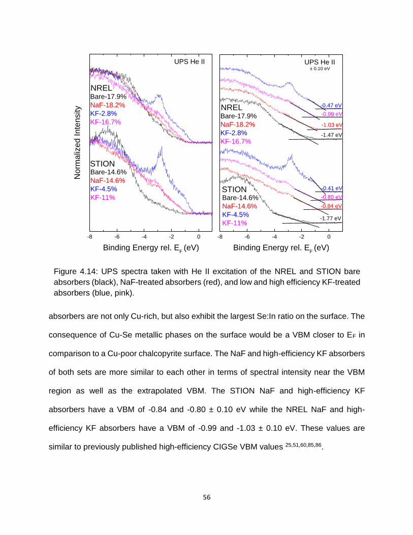
56
absorbers are not only Cu-rich, but also exhibit the largest Se:In ratio on the surface. The
consequence of Cu-Se metallic phases on the surface would be a VBM closer to EF in
comparison to a Cu-poor chalcopyrite surface. The NaF and high-efficiency KF absorbers
of both sets are more similar to each other in terms of spectral intensity near the VBM
region as well as the extrapolated VBM. The STION NaF and high-efficiency KF
absorbers have a VBM of -0.84 and -0.80 ± 0.10 eV while the NREL NaF and high-
efficiency KF absorbers have a VBM of -0.99 and -1.03 ± 0.10 eV. These values are
similar to previously published high-efficiency CIGSe VBM values 25,51,60,85,86.
-8 -6 -4 -2 0
No
rmaliz
ed Inte
nsity
Binding Energy rel. EF (eV)
Bare-14.6%
NaF-14.6%
KF-4.5%
KF-11%
STION
NRELBare-17.9%
NaF-18.2%
KF-2.8%
KF-16.7%
UPS He II
-8 -6 -4 -2 0
-1.77 eV
-0.84 eV
-0.80 eV
-0.41 eV
-1.47 eV
-1.03 eV
-0.99 eV
Binding Energy rel. EF (eV)
Bare-14.6%
NaF-14.6%
KF-4.5%
KF-11%
STION
NRELBare-17.9%
NaF-18.2%
KF-2.8%
KF-16.7%
UPS He II
-0.47 eV
± 0.10 eV
Figure 4.14: UPS spectra taken with He II excitation of the NREL and STION bare
absorbers (black), NaF-treated absorbers (red), and low and high efficiency KF-treated
absorbers (blue, pink).

57
While utilizing both XPS and UPS is advantageous to investigate the surface of
the samples, XES offers a look deeper into the bulk. Figure 4.15 presents the XES spectra
of the S L2,3 emission excited non-resonantly with an excitation of 180 eV for all four
STION absorbers. On the left, the spectra are displayed to compare spectral shape to
each other and the references above while on the right, the spectra are stacked to show
changes in intensity between the absorbers. The KF-4.5% absorber has the largest S L2,3
emission while the NaF-14.5% has the lowest. This is contrary to the XPS measurements
showing that the KF-4.5% had the least amount of S present on the surface in the set.
This suggests that the alkali-treatments are etching off S on the surface (corroborated by
XPS). In addition, there could also be a S gradient in the absorber independent of the
alkali-treatments. The STION bare absorber shows the most S on the surface (XPS),
however in the bulk (XES), it has less S than both KF absorbers. All four absorbers exhibit
similar characteristic features at ~154, 155, and 159 eV. Comparing the spectral shapes
to the reference spectra, the S in all four samples is predominantly bound to Cu and In
forming CuInS2. To take a closer look at changes between the bare absorber and the
alkali-treated absorbers, the normalized bare absorber S L2,3 emission spectra can be
subtracted from the treated absorbers and the resulting residual can be analyzed. Figure
4.16 shows the residuals of subtracting the weighted bare absorber spectrum from the
alkali-treated spectra and a comparison of the residual components to references. The
weight of the bare absorber was chosen so the resulting residual did not have negative
values. All three residuals show that there is indeed another species not evident in the
bare absorber. In fact, the two KF-treated absorbers have an additional species different

58
from the species found for the NaF absorber. The components at ~154, ~155, and ~160
eV for the KF spectra are indicative of sulfates in the absorber. The emission energy of
the main S 3s peak (~148 eV) suggests an additional In2S3 and/or Ga2S3 species not
apparent in the bare absorber spectrum.
XES measurements of both K L2,3 and F Kα can be used to determine whether
there is K and/or F in the bulk of the sample. The emission spectra of K L2,3 (left) and F
Kα (right) are presented in Figure 4.17 for the STION and NREL absorbers. The K L2,3
emission spectra show the same trends as seen on the surface: the NREL KF-treated
144 148 152 156 160 164
Norm
aliz
ed Inte
nsity
Emission Energy (eV)
XES - S L2,3
hexc.
= 180 eV
In2S
3
Cu2S
Ga2S
3
CuInS2
KF-11%
NaF-14.6%
KF-4.5%
Bare-14.6%
144 148 152 156 160 164
Norm
aliz
ed Inte
nsity
Emission Energy (eV)
XES - S L2,3
hexc.
= 180 eV
KF-11%
NaF-14.6%KF-4.5%
Bare-14.6%
STION
Figure 4.15: XES emission spectra excited nonresonantly with 180 eV of the S L2,3
region for the STION bare (black), NaF-treated (red), and low and high efficiency KF-
treated absorbers (blue, pink). Reference spectra are provided for comparison.
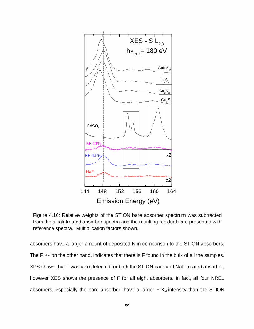
59
absorbers have a larger amount of deposited K in comparison to the STION absorbers.
The F Kα, on the other hand, indicates that there is F found in the bulk of all the samples.
XPS shows that F was also detected for both the STION bare and NaF-treated absorber,
however XES shows the presence of F for all eight absorbers. In fact, all four NREL
absorbers, especially the bare absorber, have a larger F Kα intensity than the STION
144 148 152 156 160 164
x2
CdSO4
Emission Energy (eV)
x2
XES - S L2,3
hexc.
= 180 eV
KF-11%
NaF
KF-4.5%
In2S
3
Cu2S
Ga2S
3
CuInS2
Figure 4.16: Relative weights of the STION bare absorber spectrum was subtracted
from the alkali-treated absorber spectra and the resulting residuals are presented with
reference spectra. Multiplication factors shown.

60
absorbers. Since the F is found on both the bare absorbers and the alkali-treated
absorbers, it suggests that the F may not only be from the alkali-treatments, but also a
contamination from the growth process of the absorber. Overall, the XPS, UPS, and XES
data have shown that the effects of alkali-treatments on the STION absorbers are not the
same as the NREL absorbers, although similar trends are seen within the respective
sample sets. Indeed, while there is a lot of insight and research on alkali-treated
laboratory-scale research thin-film photovoltaics, there is a need to include industry-grade
photovoltaics in these efforts with hopes of increasing overall module conversion
efficiencies.
258 259 260 261 262 263 264 265 266
No
rma
lize
d I
nte
nsity
Emission Energy (eV)
XES - K L2,3
hexc.
= 320 eV
KF-4.5%
KF-11%
STION
NRELKF-2.8%
KF-16.7%
674 675 676 677 678 679 680
Emission Energy (eV)
Bare-14.6%
NaF-14.6%
KF-4.5%
KF-11%
STION
NRELBare-17.9%
NaF-18.2%
KF-2.8%
KF-16.7%
hexc.
= 730 eVXES - F K
Figure 4.17: XES emission spectra of the K L2,3 (left) and F Kα of the NREL and STION
bare absorbers (black), NaF-treated absorbers (red), and low and high efficiency KF-
treated absorbers (blue, pink).

61
4.4 - CONCLUSION
To summarize the findings on alkali treatments of both the NREL and STION CIG(S)Se
absorbers, XPS, UPS, and XES were utilized to look at the chemical and electronic
structure of these samples. XPS shows that there is a low Ga content at surface for all
STION absorbers relative to NREL absorbers. The Ga/(Ga+In) ratio changes for the
NREL absorbers with alkali-treatments, however, the ratio does not change with the
STION absorbers. Both the STION and NREL low efficiency KF-treated absorbers have
the largest Cu:In ratio. All the alkali-treated absorbers have a low or absent Na signal on
the surface. The Na is shifted ~5 eV for the KF-2.8% absorbers, but the modified Auger
parameter suggests that it is still in a Na-Oxide bonding environment. Reduced O and
carbonate peak intensity on all Alkali-treated samples, with KF-2.8% showing a large O
1s peak at ~536 eV. F is seen in the bulk for all eight absorbers and at the surface of the
STION bare and NaF absorbers. B, Zn, and F (bulk) peaks show that there are
contaminants during the development of the absorber and/or the Alkali-treatments. The
S/Se ratio varies for all STION samples; Bare absorber shows the highest S/Se ratio,
while KF-2.8% shows the lowest. S in all STION absorbers is found mostly in a CuInS2-
like environment, with treated absorbers showing evidence of In-S and/or Ga-S bonding
environments. Both STION KF-treated absorbers and all four NREL absorbers show K at
surface and all four KF-treated absorbers have K in the bulk as well. Surface
contamination: B 1s on STION bare absorber and Zn (XPS) on the surface of both NREL
KF-treated absorbers. UPS shows that the STION bare absorber has VBM of 1.77 ± 0.10
eV (larger than expected), due to the presence of adsorbates and possibly B. The NREL
bare absorber has VBM of 1.47 ± 0.10 eV, large also due to adsorbates. The STION and

62
NREL NaF-treated absorbers have a VBM at 0.84 ± 0.10 eV and 1.03 ± 0.10 eV,
respectively, which is comparable to previously published data. The STION KF-11%
absorber has a VBM comparable to the NaF absorber in this set: 0.87 ± 0.10 eV and the
NREL KF-16.7% also has a similar VBM to the NaF absorber in respective set: 0.99 ±
0.10 eV. Both “low-efficiency” KF absorbers have similar VBM values to each other with
the STION absorber at 0.47 ± 0.10 eV and the NREL absorber at 0.41 ± 0.10 eV. The
VBM is located closer to the EF than the other absorbers, likely due to not only the large
Cu 3d band component at ~3 eV, but the large presence of Se on the surface (in
comparison to the other absorbers), potentially creating CuSe2 species.

63
CHAPTER 5
KF COEVAPORATION VS. KF POST DEPOSITION TREATMENT: SPECTROSCOPIC INVESTIGATION ON THE EFFECTS OF KF
5.1 – INTRODUCTION
With the inclusion of Na proving to be successful in chalcopyrite devices, research into
the utilization of other alkali metals became of interest11,32–38,40,41,43,117–124, especially after
EMPA raised the CIGSe world-record efficiency to 20.4% (from 18.7% for flexible
substrates and 20% for soda-lime substrates),10,103 and ZSW increased the record to
21.7% shortly after42. Both record efficiency devices utilized KF post-deposition treatment
(PDT) as the method of incorporating K, but fundamental research is needed to further
understand the role of K on the absorber and the buffer/absorber interfacial properties as
a function of K deposition parameters in order to optimize conversion efficiencies.
It is well known that Na diffuses from the soda-lime glass into the chalcopyrite
absorber34–38,122–125, however it is not known how and if the Na diffusion affects the
inclusion of K. For a more controlled inclusion of Na (K), a barrier is added to the glass
before the Mo sputter treatment to prevent such diffusion 123,126,127. It is imperative to
understand the full effects of K inclusion in the CIGSe device, especially as a function of
deposition processes, along with possible Na diffusion effects.
5.2 – EXPERIMENTAL The sample set consisted of five absorbers from NREL: two bare absorbers with and
without a SiO2 barrier, two KF-PDT treated absorbers with and without a SiO2 absorber,
and one CKIGSe absorber, for which KF was co-evaporated during the deposition of the
64
CIGSe absorber. The purpose of the SiO2 barrier is to prevent alkali atoms from diffusing
from the glass, thus allowing us to study how the KF PDT affects the CIGSe absorber. All
absorbers were grown at 525 °C with constant elemental flux profiles (i.e., not with the
NREL three-stage process) on a Mo-sputtered glass118. The efficiencies of corresponding
devices range between 9.1% (CIGSe/SiO2) and 15.5% (CKIGSe). At UNLV, the absorber
surfaces were ion-treated for a total of 60 min using 50 eV Ar+ ions at low incidence angle.
The samples were then rinsed with 100 mL H2O + 12.5 mL NH4OH at 65 °C in an inert
environment (“rinsed” and “NH4OH” will be used interchangeably in this chapter).
The absorbers were briefly exposed to air, packed, and vacuumed-sealed under
dry nitrogen before being sent to UNLV. The samples were unsealed in the inert
environment of our glove boxes, mounted, and introduced to the UHV system. XPS, UPS,
and IPES were utilized to investigate the chemical and electronic structure of the NREL
sample set. Mg Kα and Al Kα irradiation and a SPECS PHOIBOS 150 MCD electron
analyzer were employed for XPS measurements while a He discharge lamp and He II
excitation were employed for the UPS measurements. A custom-built Dose-type detector
with a SrF2 window and Ar:I2 filling,81 along with a commercial low-energy electron gun
(Staib), were used for IPES experiments. The spectra were calibrated using Auger and
core-level peaks of clean Cu, Ag, and Au foils (XPS)80 and the Fermi energy of a clean
Au foil (UPS, IPES).
All peaks were analyzed by fitting the different spectral intensities with Voigt
functions (with coupled Lorentzian and Gaussian widths) and a linear background using
the Fityk peak-fitting program90. The VBM and CBM were determined by linear
extrapolation of the leading edge in the valence band (UPS) and conduction band (IPES)

65
spectra109. The base pressure in the UNLV analysis chamber was better than 5×10⁻¹⁰
mbar.
5.3 – RESULTS AND DISCUSSION
Figure 5.1 shows the XPS Mg Kα survey spectrum taken on all five samples after ion-
treatment (black) and NH4OH rinse (red). All expected peaks (Cu, In, Ga, Se, Na) are
present (no Na on ion-treated absorbers with SiO2 barrier, as will be discussed later),
along with adsorbates, C and O. All spectra were normalized to the In 3d5/2 peak in order
to compare peak ratios to In. Detail spectra of the Cu 2p3/2 of the current sample set (left)
and a comparison with a previous NREL alkali-treated sample set (chapter 4) are shown
in Figure 5.2. It compares the effects of the rinse, KF-PDT, and co-evaporated KF on the
1200 1000 800 600 400 200 0NH
4OH
NH4OH
NH4OH
NH4OH
KF PDT/SiO2
CIGSe/SiO2
CKIGSe
KF PDT
Inte
nsity N
orm
aliz
ed
to
In
3d
5/2 A
rea
Binding Energy (eV)
F 1sK LMM
K 2s
XPS Mg K
Na KLL
Se 3s
Cu
3s/In
4s
Cu
3p
/In
4p
Cu LMM
C 1sIn
4d
/Ga
3d
Se 3d
Ga 3p
Se 3p
Ga 3s
Ga LMM
K 2pO 1s
In 3d
In 3p
O K
LL
In 3s
In M
NN
Cu 2p
C K
VV
Ga 2p
Na 1s
F KLL
CIGSe
NH4OH
Figure 5.1: XPS Mg Kα survey spectrum taken of the NREL bare and KF-treated
absorbers. The ion-treated surfaces are shown in black, while the rinsed surfaces are
shown in red.

66
NREL samples, and also shows the differences between the 3-stage coevaporation
process (bottom) and constant elemental flux (center, top). For the center and top spectra,
normalizing the Cu 2p3/2 peak to the In 3d5/2 area, shows that there is a Cu depletion at
the surface of both KF PDT absorbers that is still present after the ammonia treatment.
The Cu depletion is also seen for the “high-efficiency” three-stage KF-PDT and NaF-PDT
NREL absorbers (right). The Cu:In ratio from the 3-stage co-evaporation CIGSe absorber
(“Bare-17.9%”) is much smaller than for the CIGSe absorber grown with constant
elemental flux (left). The surfaces of the bare and CKIGSe absorber of the current sample
set are not Cu-poor. After the rinse, the Cu:In ratio increases for the CIGSe/SiO2 and
938 936 934 932 930 928
NH4OH
Inte
nsity N
orm
aliz
ed
to
In
3d
5/2 A
rea
Binding Energy (eV)
Cu 2p3/2
KF PDT/SiO2
CIGSe/SiO2
XPS Mg K
KF PDT
CIGSe
CKIGSe
3-stage coevap
KF-16.7%
NaF-18.2%
Bare-17.9%
KF-2.8%
Figure 5.2: Detailed XPS Mg Kα spectra of the Cu 2p3/2 taken on the ion-treated
(center) and NH4OH treated (top) of the CKIGSe, both CIGSe, and both KF PDT
absorbers. This is compared to a previous sample set, displayed on the bottom (four
alkali-treated NREL absorbers, grown with the three-stage coevaporation process).

67
CKIGSe, but there is no change for the CIGSe absorber. All alkali-treated absorbers and
the CIGSe/SiO2 absorber are shifted towards lower binding energy (BE) in relation to the
CIGSe. There is also no evidence for Cu-F or Cu-O species.
The detail spectra in Figure 5.3 present the Se 3d peak normalized to In 3d5/2 area
(left) and peak height (right). When normalizing the Se 3d peak to the In 3d5/2 peak, it is
clear that the KF PDT absorbers both have lower surface Se:In ratios. After the NH4OH
treatment, the Se:In ratio for the KF PDT absorbers reduce by almost half, while the ratio
stays relatively constant for the CKIGSe and both CIGSe absorbers. There are also no
Se-oxides on the surface, evident by the lack of a peak at ~ 59 eV. Normalizing the Se
3d to peak height, it is easier to see shape changes and shifts. In particular, the unrinsed
60 59 58 57 56 55 54 53 52 51 50
Binding Energy (eV)
KF PDT/SiO2
CIGSe/SiO2
KF PDT
CIGSe
CKIGSe
NH4OH
XPS Mg K
Se 3d
Inte
nsity N
orm
aliz
ed t
o In
3d
5/2 A
rea
SeOx
60 59 58 57 56 55 54 53 52 51 50
NH4OH
No
rmaliz
ed
Inte
nsity
Binding Energy (eV)
KF PDT/SiO2
CIGSe/SiO2
KF PDT
CIGSe
CKIGSe
XPS Mg K
Se 3d
SeOx
Figure 5.3: Detailed XPS Mg Kα spectra of the Se 3d region, normalized by In 3d5/2
area (left) and peak height (right). The ion-treated spectra are shown at the bottom,
and the NH4OH treated spectra at the top. The expected locations for oxide
contributions are indicated.

68
KF PDT absorber exhibits a wider shape and a shoulder at 57 eV that is reduced with the
NH4OH treatment. References111,112 suggest a Se-C bonding environment, which is
commensurate with the fact that this absorber shows the largest amount of C on the
surface (as will be discussed later in conjunction with Figure 5.13). There is no evidence
for the presence of a Se-O bonding environment on any of the absorber surfaces (SeOx
species would appear at ~59 eV). After rinsing, the Se 3d peaks for all absorbers shift
slightly to lower binding energies.
The In 3d5/2 (left) and In MNN (right) regions exhibit unusual peak shapes for both
KF PDT absorbers, as shown in Figure 5.4. The spectra are again normalized to peak
449 448 447 446 445 444 443 442 441
NH4OH
Norm
aliz
ed Inte
nsity
Binding Energy (eV)
In2Se
3
In2O
3
In 3d5/2
XPS Mg K
InF3
KF PDT/SiO2
CIGSe/SiO2
KF PDTCIGSe
CKIGSe
390 393 396 399 402 405 408 411 414
NH4OH
No
rma
lize
d I
nte
nsity
Kinetic Energy (eV)
XPS Mg K
In MNN
CIGSeKF PDTCKIGSe
CIGSe/SiO2
KF PDT/SiO2
Figure 5.4: Detailed XPS Mg Kα spectra of the In 3d5/2 (left) and In MNN (right) regions,
normalized by peak height. The ion-treated spectra are shown at the bottom, while the
NH4OH-treated spectra are at the top. The expected locations for oxide, selenide, and
fluoride contributions are indicated.

69
height (in the case of the In MNN, the most prominent peak at ~408 eV was used). In
XPS, both unrinsed KF PDT absorbers have a large shoulder at ~446.5 eV, suggesting
the presence of an In-F bonding enviroment. These two peaks are also wider than those
of the CKIGSe and both CIGSe absorbers, suggesting the presence of oxides as well.
The NH4OH treatment reduces the amount of In-F and shifts both KF PDT absorbers
towards higher BE, while CKIGSe and both CIGSe absorbers shift toward lower BE,
suggesting reduction of oxides, as will be discussed in more detail in the following.
The In MNN region is particularly useful to discern the presence of oxides, as it
offers a more distinct peak position difference between In-Se and In-O bonding
396 399 402 405 408 411 414
Norm
aliz
ed Inte
nsity
Kinetic Energy (eV)
In-Se
In-O
KF PDT (unrinsed)
XPS Mg K
In-F(x0.35)
(x0.65)
(x0.62)
396 399 402 405 408 411 414
(x0.66)
(x0.53)In-Se
In-O
Norm
aliz
ed Inte
nsity
Kinetic Energy (eV)
KF PDT - NH4OH
XPS Mg K
In-F (x0.10)
Figure 5.5: Detailed XPS Mg Kα spectra In MNN region, normalized by peak height,
for the clean and rinsed KF PDT absorbers. Three In-Se references are used to fit the
peaks to show contributions from In-F, In-O, and In-Se species. The residual is shown
on the bottom in purple.

70
environments128. The most striking feature is the overall shape of the In MNN peaks of
both KF PDT absorbers in comparison to the other absorbers. Pre-rinse, the In MNN
region for both KF PDT absorbers is a superposition of (at least) three species, most likely
In-F, In-O, and In-Se bonding environments. After the NH4OH treatment, we find a clear
reduction in the In-F species (seen in both graphs). However, we also observe an
increase in In-O species for both KF PDT absorbers, seen by the peak at ~405 eV. This
peak is larger for the KF PDT/SiO2 absorber (than for the KF PDT absorber), indicating
the presence of more In-O species. Amongst CKIGSe and both CIGSe absorbers, the
CIGSe shows the least amount of oxides, as seen by the deepest “dip” at ~405 eV.
CKIGSe and CIGSe/SiO2 both exhibit more shallow dips and a shoulder at ~399 eV. After
the NH4OH treatment, the dip is similar for these three absorbers, but slightly deeper for
the CIGSe/SiO2 absorber. This is also seen in the region 390-399 eV, where the spectral
intensity is lower. The NH4OH treatment removes/reduces oxides for CKIGSe and both
CIGSe absorbers, but adds oxides to the surface of both KF PDT absorbers. In contrast,
the NH4OH treatment reduces the In-F species on the surface of these two absorbers,
best seen in Figure 5.5. The In MNN spectra of the pre and post-rinse KF PDT absorber
were fit with an In-Se reference (ion-treated CIGSe absorber), shifted to reflect
contributions from In-O and In-F. After the rinse there is a clear decrease in In-F
contributions (from x0.35 to x0.10) and increase in In-O (from 0.62x to 0.66x). The quality
of the residual shows that three species can fit the spectra pretty well. Note, it is more
difficult to fit a spectrum using other spectra than using functions hence a more poor
residual is expected.
In addition to the presence of an In-F species on the surface of the KF PDT

71
absorbers, we find indications for the presence of a Ga-F species as well. Figure 5.6
shows survey spectra of Ga 2p3/2 (left) and Ga LMM (right). The Ga 2p3/2 peaks for both
KF PDT absorbers are shifted ~ 2eV towards higher BE, which corresponds to a Ga-F
bonding enviroment. Normalizing the Ga 2p3/2 peak to In 3d5/2 shows that the Ga:In ratio
is smallest for both KF PDT absorbers, and largest for the CIGSe absorber before the
NH4OH treatment. After the treatment, we find a Ga signal reduction at the surface for all
the absorbers, most notably for the KF PDT absorbers. After the NH4OH treatment, the
CIGSe/SiO2 absorber surface shows the largest Ga:In ratio, albeit half of the original
peak.
The Ga LMM peak shape gives a good indication for the presence of Ga-oxides.
1124 1122 1120 1118 1116 1114
NH4OH
Inte
nsity N
orm
aliz
ed to In 3
d5
/2 A
rea
Binding Energy (eV)
GaF3
XPS Mg K
Ga 2p3/2
Ga2Se
3
Ga2O
3
KF PDT/SiO2
CIGSe/SiO2
KF PDT
CIGSe
CKIGSe
1056 1059 1062 1065 1068 1071 1074
NH4OH
Inte
nsity N
orm
aliz
ed to In 3
d5
/2 A
rea
Kinetic Energy (eV)
GaF3
Ga2O
3
Ga2Se
3
XPS Mg K
Ga LMM
KF PDT/SiO2
CIGSe/SiO2
KF PDT
CIGSe
CKIGSe
Figure 5.6: Detailed XPS Mg Kα spectra of the Ga 2p3/2 (left) and Ga LMM (right)
regions, normalized by the In 3d5/2 area. The ion-treated spectra are shown at the
bottom, while the NH4OH-treated spectra are at the top. The expected locations for
oxide, selenide, and fluoride contributions are indicated.

72
For instance, we observe an extra component at ~1062 eV for the unrinsed CKIGSe and
CIGSe/SiO2 absorbers that is removed after the NH4OH treatment. The Ga LMM peaks
for both KF PDT absorbers are shifted towards lower KE and the primary peak positions
match that of Ga-F. After the NH4OH treatment, the Ga LMM peaks are reduced,
especially for the KF PDT absorbers. The Ga-O and Ga-F species are removed. The
CIGSe/SiO2 absorber shows the largest Ga LMM peak, similar to the Ga 2p3/2 peak.
The Ga 3d/In 4d region offers the opportunity to measure how the Ga/(Ga+In) ratio
changes amongst the samples before and after the NH4OH treatment, as depicted in
23 22 21 20 19 18 17 16
CIGSe
KF PDT
CKIGSe
CIGSe/SiO2
Ga 3d
No
rmaliz
ed
Inte
nsity
Binding Energy (eV)
XPS Mg K In 4d
NH4OH
KF PDT/SiO2
Figure 5.7: Detailed XPS Mg Kα spectra of the Ga 3d and In 4d region. The dotted
spectra represent NH4OH treated absorbers while the continuous line spectra
represent the “clean” surfaces. Regions where Ga 3d and In 4d peaks are located are
boxed.

73
21 20 19 18 17 16
Norm
aliz
ed Inte
nsity
Binding Energy (eV)
x3
XPS Mg K
Ga 3d / In 4d
Ga/(In+Ga)
0.30 0.10 eV
CIGSeUnrinsed
In 4d
Ga 3d
21 20 19 18 17 16
Norm
aliz
ed Inte
nsity
Binding Energy (eV)
x3
XPS Mg K
Ga 3d / In 4d
Ga/(In+Ga)
0.25 0.10 eV
CIGSeRinsed
In 4d
Ga 3d
21 20 19 18 17 16
Norm
aliz
ed Inte
nsity
Binding Energy (eV)
x3
XPS Mg K
Ga 3d / In 4d
Ga/(In+Ga)
0.33 0.10 eV
CIGSe/SiO2
Unrinsed
Ga 3d
In 4d
21 20 19 18 17 16
No
rmaliz
ed
Inte
nsity
Binding Energy (eV)
x3
XPS Mg K
Ga 3d / In 4d
Ga/(In+Ga)
0.19 0.10 eV
CIGSe/SiO2
Rinsed
In 4d
Ga 3d
Figure 5.8: XPS detail spectra of the Ga 3d/In 4d of the pre and post-rinse CIGSe
absorber (top) and CIGSe/SiO2 (bottom). Fit curves for In:Ga contributions to the
peak are shown along with their respective residuals (purple).

74
Figure 5.7. The unrinsed absorber spectra are plotted with a continuous line while the
dotted spectra represent the NH4OH treated absorbers. Clear changes are seen amongst
the samples themselves and between pre-rinse and post-rinse spectra. The pre-rinse KF
PDT and KF PDT/SiO2 spectra are broadest suggesting the presence of multiple species.
After the rinse, the spectra are more narrow and shifted towards higher BE. The CIGSe,
CKIGSe, and CIGSe/SiO2 absorbers exhibit more similar peak shapes and they all shift
towards lower BE.
The In and Ga components to the spectra are shown by fitting the data. Pre-rinse
and post-rinse fits for the CIGSe and CIGSe/SiO2 are shown in Figure 5.8, CKIGSe in
Figure 5.9, and KF PDT and KF PDT/SiO2 in Figure 5.10. The peaks were fit with a linear
21 20 19 18 17 16
Norm
aliz
ed Inte
nsity
Binding Energy (eV)
x3
XPS Mg K
Ga 3d / In 4d
Ga/(In+Ga)
0.30 0.10 eV
CKIGSeUnrinsed
Ga 3d
In 4d
21 20 19 18 17 16
Norm
aliz
ed Inte
nsity
Binding Energy (eV)
x3
XPS Mg K
Ga 3d / In 4d
Ga/(In+Ga)
0.23 0.10 eV
CKIGSeRinsed
In 4d
Ga 3d
Figure 5.9: XPS detail spectra of the Ga 3d/In 4d region of the CKIGSe absorber pre-
rinse (left) and post-rinse (right). Fit curves for In:Ga contributions to the peak are
shown along with their respective residuals (purple).

75
background and Voigt profiles, using coupled Gaussian widths for all components, and
coupled but separate Lorentzian widths for In and Ga, respectively. The ratios of the spin-
orbit split peaks were fixed according to their multiplicity, along with their respective peak
separation, 0.86 eV for In113,114 and 0.46 eV for Ga115. The data is shown with black dots,
the In 4d and Ga 3d components in black, and the resulting fit in red for Figures 5.8 and
5.9. The residual of the fit is shown below each spectrum (purple). These shallow core
levels already possess some band character, and thus the quality of the fit is very
surprisingly high, especially given all the above-mentioned boundary conditions included
in the fit. The surface Ga/(Ga+In) ratio for the pre-rinsed CIGSe and CIGSe/SiO2
absorbers samples are 0.30 and 0.33 (± 0.10), respectively, indicating a very small
change in the surface ratio with the addition of the SiO2 barrier. This is different than what
the Ga 2p detailed region shows but is similar to what the Ga LMM presents. It is
speculated that since the CIGSe/SiO2 absorber has a larger O 1s and C 1s peak (as will
be discussed in conjunction with Figures 5.13 and 5.15 later), the low KE (high BE) peaks
would be more attenuated than the CIGSe absorber and higher KE peaks. After the
NH4OH treatment, the Ga/(Ga+In) ratio decreases: 0.25 ± 0.10 eV for the CIGSe absorber
and 0.27 ± 0.10 eV for CIGSe/SiO2 indicating a small Ga depletion at the surface after
the rinse. For CKIGSe, the pre-rinse surface Ga/(Ga+In) ratio is similar to both CIGSe
and CIGSe/SiO2, 0.30 ± 0.10 eV, and exhibits a slightly larger Ga-depletion on the surface
after the rinse, 0.23 ± 0.10 eV.
Figure 5.10 portrays the fits for the pre and post-rinse KF PDT and KF PDT/SiO2
surfaces. Due to the broadness of the peaks, several species are expected to contribute
to the overall spectra and are indicated with In-Se in black, In-O in pink, In-F in teal, Ga-

76
23 22 21 20 19 18 17 16
Ga/(In+Ga)
0.16 0.10 eV
In-Se
In-O
Norm
aliz
ed Inte
nsity
Binding Energy (eV)
x3
XPS Mg K
Ga 3d / In 4d
KF PDTUnrinsed
In-F
Ga-F
21 20 19 18 17 16
No
rmaliz
ed
Inte
nsity
Binding Energy (eV)
x2
XPS Mg K
Ga 3d / In 4d
Ga/(In+Ga)
0.05 0.10 eV
KF PDTRinsed
In-Se
In-O
Ga-Se
22 21 20 19 18 17 16
Norm
aliz
ed Inte
nsity
Binding Energy (eV)
In-O
x3
XPS Mg K
Ga 3d / In 4d
Ga/(In+Ga)
0.05 0.10 eV
KF PDT/SiO2
Unrinsed
In-FGa-F
In-Se
21 20 19 18 17 16
Norm
aliz
ed Inte
nsity
Binding Energy (eV)
x3
XPS Mg K
Ga 3d / In 4d
Ga/(In+Ga)
0.14 0.10 eV
KF PDT/SiO2
Rinsed
In-Se
In-O
Ga-Se
Figure 5.10: XPS detail spectra of the Ga 3d/In 4d region of the pre and post-rinse
KF PDT absorber (top) and KF PDT/SiO2 (bottom). Fit curves for In:Ga contributions
to the peak are shown along with their respective residuals (purple).

77
F in black, and Ga-Se in purple. In contrast, the In 4d and Ga 3d peaks depicted in Figures
5.8 and 5.9 are indicative of In-Se and Ga-Se species. The presence of multiple species
for the KF PDT absorbers is corroborated by the In 3d, In MNN, Ga 2p, and Ga LMM
spectra seen previously. The peaks were identified according to references111,112 and their
peak separations fixed amongst all the spectra. With a KF PDT on the absorber, Ga-
depletion already occurs in comparison with the CIGSe and CIGSe/SiO2 absorbers. The
Ga/(Ga+In) ratio for the pre-rinse KF PDT absorber and KF PDT/SiO2 absorber are 0.16
± 0.10 eV and 0.05 ± 0.10 eV, respectively. The ratios suggest that with the addition of
the SiO2 barrier, the Ga-depletion on the surface is even more pronounced. After the
NH4OH treatment, the Ga components shift to lower binding energies (note the loss of
the shoulder at 22 eV) indicative of Ga-Se111,112 (also seen with Ga LMM). The Ga 3d/In
4d region after the NH4OH treatment is narrower for both samples. As a result, the peaks
could be fit with only two In species instead of three but that is not to say the third species
is gone. Adding a third species did not further enhance the residual, and in the case of
the rinsed KF PDT fit, it was detrimental to the other fits. The peak s are labeled as In-O
and In-Se due to their peak locations and evidence for a big reduction of In-F, but small
reduction of In-Se and an increase in In-O as seen in the n MNN spectra. The resulting
Ga/(Ga+In) ratio shows that the KF PDT surface exhibits an even more Ga-poor surface
while the ratio for the KF PDT/SiO2 absorber almost tripled (0.07 ± 0.10 eV and 0.14 ±
0.10, respectively). Overall, the Ga/(Ga+In) ratio of the KF PDT absorbers shows that the
treatment creates a more Ga-poor surface than the CIGSe and CKIGSe counterparts.
An inherent property of fitting peaks is that the more functions you add, the fit gets
better. However, the functions need to be accounted for and they need to serve a purpose

78
23 22 21 20 19 18 17 16
Norm
aliz
ed In
ten
sity
Binding Energy (eV)
x3
XPS Mg K
Ga 3d / In 4dKF PDTUnrinsed
In species
Ga
species
23 22 21 20 19 18 17 16
No
rmaliz
ed
Inte
nsity
Binding Energy (eV)
x3
XPS Mg K
Ga 3d / In 4d
KF PDTUnrinsed
In species
Ga
species
23 22 21 20 19 18 17 16
Norm
aliz
ed Inte
nsity
Binding Energy (eV)
x2
XPS Mg K
Ga 3d / In 4d
KF PDTUnrinsed
In species
Ga
species
23 22 21 20 19 18 17 16
Norm
aliz
ed Inte
nsity
Binding Energy (eV)
x2
XPS Mg K
Ga 3d / In 4dKF PDTUnrinsed
In species
Ga
species
Figure 5.11: XPS detail spectra of the Ga 3d/In 4d region of the pre-rinse KF PDT
absorber as a function of fit curves to show the process of determining a good fit. Fit
curves for In:Ga (In 4d5/2, In 4d3/2, Ga 3d5/2, Ga 3d3/2) contributions to the peak are
shown along with their respective residuals (purple).

79
in the fit. The KF PDT absorbers both required more components to fit the Ga 3d/In 4d
region than the other samples and an example of the fitting process is presented in Figure
5.11. On the bottom right, the Ga 3d/In 4d region is only fit with 5 total components: a
linear background, In 4d5/2, In 4d3/2, Ga 3d5/2, and Ga 3d3/2. The residual, shown below
the fit, exhibits a sinusoidal shape indicative of a poor fit of the peak. With the addition of
two more components (bottom left), representing the In 4d peaks, The resulting residual
shows more statistical noise towards higher binding energies, but the fit towards lower
binding energies is still poor. With the addition of another set of two components (top
right), representing In 4d again, the fit of the peak is much better (note the magnification
difference between the bottom two fits and the top two fits). Not only this, but the
components can all be accounted for using evidence of other XPS detailed regions. The
top left graph displays a fit with two more additional components, representing Ga 3d,
however, there is not a significant improvement in the residual of the fit in comparison to
the top right fit. Thus, the top right fit is used to describe the Ga 3d/In 4d region of the
unrinsed KF PDT absorber.
To summarize our findings thus far, the analysis of the Cu, In, Ga, and Se
photoemission and Auger peaks shows no evidence of Se and Cu oxides and fluorides,
but evidence of Ga and In oxides and fluorides. We see a surface depletion of Cu and Se
with the KF PDT that is even further reduced with the NH4OH treatment. So far, we see
that the KF PDT affects the surface of the CIGSe absorbers similarly for both the absorber
with the SiO2 barrier and the absorber without, while there are clear differences between
the two untreated absorbers. The bare absorber without the SiO2 barrier exhibits a larger
Cu:In ratio (compared to its counterpart), but after the NH4OH treatment, it is the

80
CIGSe/SiO2 absorber that shows the larger Cu:In ratio. The CIGSe/SiO2 absorber exhibits
a slightly larger Ga/(Ga+In) ratio than the CIGSe absorber. The surface of the CKIGSe
absorber is found to be more similar to the CIGSe (with and without SiO2) absorbers, than
the KF PDT absorbers, indicating that not only the addition of K but also the deposition
method of KF plays an important role for the surface properties. The KF absorbers exhibit
a strong Cu and Ga-depletion on the surface with the KF PDT absorber displaying the
larger Cu:In and Ga/(Ga+In) ratios before the NH4OH treatment. After the treatment, the
KF PDT still has the larger Cu:In ratio, but the KF PDT/SiO2 presents a larger Ga/(Ga+In)
ratio. The ratio change for the KF PDT/SiO2 suggests that either the deposition of Ga on
692 690 688 686 684 682 680
NH4OH InF
3KF
Inte
nsity N
orm
aliz
ed
to
In
3d
5/2 A
rea
Binding Energy (eV)
F 1s XPS Mg K
NaF
KF PDT/SiO2
CIGSe/SiO2
KF PDTCIGSe
CKIGSe
692 690 688 686 684 682 680
NH4OH
CF2
Inte
nsity N
orm
aliz
ed
to
In
3d
5/2 A
rea
Binding Energy (eV)
InF3
KF
F 1s
KF PDT/SiO2
CIGSe/SiO2
XPS Mg K
KF PDTCIGSe
CKIGSe
NaF
Figure 5.12: Detailed XPS Mg Kα spectra of the F 1s region, normalized by the In
3d5/2 area. The ion-treated spectra are shown at the bottom, while the NH4OH-treated
spectra are at the top (left). The right graph is scaled to see the F 1s peaks of the
NH4OH treated absorbers (only). The expected locations for InF3, NaF, KF, and CF3
contributions are indicated.

81
the surface occurred during the NH4OH treatment, or Ga diffused to the surface from the
bulk.
Analyzing the F peaks also offers direct insights into the local bonding
environments on the surface. Figure 5.12 shows the presence of a F 1s signal for both
the KF PDT absorbers and the CKIGSe absorber. The KF PDT peak is broader and
larger than for KF PDT/SiO2 and CKIGSe, suggesting multiple species (corroborating the
earlier evidence for the presence of Ga-F and In-F bonds). The KF PDT/SiO2 absorber is
also broad and shows a larger tail towards ~682 eV, indicative of KF. This is supported
by the KF peak intensities in Figure 5.6, where KF/SiO2 shows the largest peak. The
300 295 290 285 280
NH4OH
Kmet
Ga L3M
23M
45
Ga L3M
23M
45
Inte
nsity N
orm
aliz
ed
to
In
3d
5/2 A
rea
Binding Energy (eV)
K 2p
C 1s
KF PDT/SiO2
CIGSe/SiO2
XPS Mg K
KF PDTCIGSe
CKIGSe
KF
300 298 296 294 292 290
NH4OH K
met
Inte
nsity N
orm
aliz
ed
to
In
3d
5/2 A
rea
Binding Energy (eV)
K 2p
KF PDT/SiO2
CIGSe/SiO2
XPS Mg K
KF PDTCIGSe
CKIGSe
KF
Figure 5.13: Detailed XPS Mg Kα spectra of the C 1s and K 2p region, normalized by
the In 3d5/2 area (left). The ion-treated spectra are shown at the bottom, while the
NH4OH-treated spectra are at the top (left). The right graph is magnified to show the
K 2p peaks of the NH4OH and ion-treated absorbers. The expected locations for Ga
LMM, KF, and metallic K (Kmet) are indicated.

82
CKIGSe F 1s peak is shifted towards lower BE, matching the BE range of NaF. On this
scale, it appears that, after rinsing the absorbers, F is completely removed. However,
closer inspection (Fig. 5.12 right) suggests otherwise. On this scale, it is clear that both
KF PDT absorbers show F on the surface, with KF PDT/SiO2 having one species that
aligns well with In-F, and KF PDT having at least two species, most likely In-F and C-F.
The NH4OH treatment definitely reduces the F on the absorber surfaces, but it is not
completely removed for the KF PDT absorbers.
Having established the presence of F on the various surfaces, we now turn to K.
Detailed spectra of the C 1s and K 2p peaks are presented in Figure 5.13. In the C 1s
plot on the left, all absorbers show C on the surface; however, both unrinsed KF PDT
absorbers show the most. The spectral intensity between 287 and 291 eV is also quite
large, possibly a combination of inelastically scattered electrons from the C 1s peak and
the presence of multiple species, for example carbonates at 290 eV. This is further
corroborated by the “dip” at ~291 eV seen for the KF PDT/SiO2 absorber that is absent
for the KF PDT absorber (even though this absorber shows more C and less K). Relative
to the unrinsed KF-PDT absorbers, the C 1s peaks of the unrinsed CKIGSe and the two
CIGSe absorbers are shifted towards lower BE. However, after the NH4OH treatment, we
find more C on the surface of CKIGSe and both CIGSe absorbers, while there is a
significant decrease in C for both KF PDT absorbers (note that the shoulder at ~283 eV,
which becomes more pronounced after the rinse, is a Ga LMM Auger line). K 2p peaks
are visible for the unrinsed KF PDT absorbers, and very small peaks can also be seen
for the unrinsed CKIGSe absorber (Figure 5.13, right), indicating that there is a lower
concentration of K on the surface for the coevaporation process relative to PDT treatment.

83
The KF PDT/SiO2 absorber shows the largest K 2p peaks before the rinse, and they shift
towards lower BE relative to the KF PDT absorber. Magnifying the intensity scale (Figure
5.13, right), we also find a K 2p peak for the CKIGSe absorber, albeit very small. Like in
the case of F, the KF coevaporation deposition does show traces of K on the surface.
After the NH4OH treatment, the K is removed from KF PDT/SiO2 absorber, but it is still
present for the CKIGSe (slightly reduced) and KF PDT (greatly reduced). The K peak
position on both KF PDT absorbers before the rinse is indicative of a K-F bonding
environment. For CKIGSe, the K 2p BE position is shifted towards higher BE.
The Na 1s region for the ion- and NH4OH-treated absorbers are compared in
1076 1074 1072 1070
Na-O
No
rma
lize
d I
nte
nsity to
In
3d
5/2 A
rea
Binding Energy (eV)
XPS Mg K
Na 1s
NaF
KF PDT/SiO2
CIGSe/SiO2
KF PDTCIGSe
CKIGSe
NH4OH
1076 1074 1072 1070
NH4OH
No
rma
lize
d I
nte
nsity to
In
3d
5/2
Are
a
Binding Energy (eV)
KF PDT/SiO2
CIGSe/SiO2
KF PDTCIGSe
CKIGSe
XPS Mg K
Na 1s
Figure 5.14: Detailed XPS Mg Kα spectra of the Na 1s region, normalized by the In
3d5/2 area. The ion-treated spectra are shown at the bottom, while the NH4OH-treated
spectra are at the top (left). The right graph is scaled to show the Na 1s peaks of the
NH4OH-treated absorbers (only). A line was drawn to help guide the eye. On the left,
the expected locations for NaF and NaO contributions are indicated.

84
Figure 5.14. The effects of the SiO2 barrier are clearly seen in the ion-treated spectra, in
which there is no detectable Na peak on the surface of the samples with barrier. Among
the barrier-free absorbers, the ion-treated KF PDT absorber shows the largest Na peak,
almost triple the size of the CKIGSe Na peak. The Na peaks are broad and asymmetric,
suggesting the presence of multiple species, including Na oxides and/or NaF. NaF
species would make more sense on the CKIGSe and KF PDT absorbers since Figure 6
shows there is indeed F on the surface. Figure 5.14, right, presents magnified spectra of
the NH4OH-treated absorbers. We find trace amounts of Na on all five samples, including
the absorbers with SiO2 barrier, which might have been deposited during the NH4OH
treatment. A modified Auger parameter, α’, plot aids in identifying potential species using
both the Na KLL and Na 1s peak separation. All of the absorbers range between the α’
2060 and 2063 eV along with all of the Na-oxide species. It is clear that the Na on the
absorbers are not metallic. The rinsed CIGSe/SiO2 has the same α’ as NaHCO2,
NaOOCH, and Na2SO4 indicating that these are possible chemical environments for these
two absorbers. Na2SO4 can be ruled out since there is no S on the samples. The pre-
rinsed KF PDT absorber lies in between Na2O and NaF and the α’ could be a convolution
of the two species. Figure 5.14 shows the Na 1s peak for this absorber and the broadness
of the peak suggests multiple species. The α’ plot shows that the Na on all of the absorber
surfaces exhibits some Na-O bonding.
The variance in adsorbates on the absorber surfaces can clearly be seen in the O
1s spectra in Figure 5.16. Both, changes in the peak intensities (left) and peak position
and shape (right) are evident. The KF PDT absorbers have the largest O 1s peaks, both
before and after NH4OH treatment. The peak shapes for all the absorbers, pre and post-

85
1073.0 1072.5 1072.0 1071.5 1071.0 1070.5
988
989
990
991
992
993
994
995
2059
2060
NaF
Not Rinsed
NaOOCH
NaHCO3
Na2SO
4
Na2CO
3
Na2SO
3
Na2S
2O
n
CIGSe/SiO2
CKIGSeCIGSe
KF PDT/SiO2
KF PDT
CKIGSe
KF PDT
CIGSe
Na
K L
2,3L
2,3
Kin
etic E
ne
rgy (
eV
)
Na 1s Binding Energy (eV)
2061
2062
2063
2064
2065
Na2SeO
3
Na2C
2O
4
Na
Na2O
Rinsed
'
Figure 5.15: Modified Auger Parameter plot of Na 1s and Na KLL. The ion-treated data
are shown in red, the NH4OH treated data in blue, and references (111,112) in black.

86
rinse, are asymmetrical and broad, suggesting multiple O species, mostly contributions
from hydroxides and surface adsorbates. The changes in peak shapes and binding
energies indicate a change in the relative amounts of hydroxide and oxide contributions.
For example, the CKIGSe O 1s shifts almost 2 eV towards higher BE after the rinse,
where the peaks of H2O and OH are expected. Fits of these peaks are presented in
Figures 5.17, 5.18, and 5.19. The peaks were fit with a linear background, identical
Gaussian and Lorentzian widths, and fixed positions for all species. The residuals shown
below the spectra indicate that the quality of the fit is quite high for all the surfaces. Peak
assignments were determined utilizing references111,112,129. The unrinsed CIGSe,
538 536 534 532 530 528
NH4OH
KF PDT/SiO2
CIGSe/SiO2
Inte
nsity N
orm
aliz
ed to
In 3
d5
/2 A
rea
Binding Energy (eV)
H2O carbonates
O-HXPS Mg K
O 1s
KF PDT
CIGSe
CKIGSe
metal oxides
538 536 534 532 530 528
NH4OH
No
rma
lize
d In
ten
sity
Binding Energy (eV)
KF PDT/SiO2
CIGSe/SiO2
H2O carbonates
O-HXPS Mg K
O 1s
KF PDT
CIGSe
CKIGSe
metal oxides
Figure 5.16: Detailed XPS Mg Kα spectra of the O 1s region, normalized by the In 3d5/2
area (left) and O 1s peak height (right). The ion-treated spectra are shown at the
bottom, while the NH4OH-treated spectra are at the top. The expected locations for
water, hydroxide, metal oxides, and carbonates are indicated.

87
540 538 536 534 532 530 528
OH''
OH'
No
rmaliz
ed Inte
nsity
Binding Energy (eV)
XPS Mg K
CIGSeO 1s
metal-oxide
540 538 536 534 532 530
Binding Energy (eV)
No
rmaliz
ed Inte
nsity
XPS Mg K
Rinsed CIGSe
O 1s
OH''
metal-oxide
OH'
540 538 536 534 532 530
No
rmaliz
ed Inte
nsity
Binding Energy (eV)
XPS Mg K
CIGSe/SiO2
O 1s
OH''
metal-oxide
OH'
540 538 536 534 532 530
Norm
aliz
ed Inte
nsity
Binding Energy (eV)
XPS Mg K
Rinsed
CIGSe/SiO2
O 1s
OH''
metal-oxide
OH'
Figure 5.17: XPS detail spectra of the O 1s peak and fit (components in black, sum
in red) of the pre and post-rinsed CIGSe (top) and CIGSe/SiO2 samples (bottom).

88
540 538 536 534 532 530 528
metal-oxide
Binding Energy (eV)
No
rmaliz
ed
Inte
nsity
XPS Mg K
KF PDT
O 1s
carbonate
OH'
540 538 536 534 532 530 528
Binding Energy (eV)
No
rmaliz
ed
Inte
nsity
XPS Mg K
Rinsed KF PDT
O 1s
metal-oxide
carbonate
OH'
540 538 536 534 532 530
No
rma
lize
d I
nte
nsity
Binding Energy (eV)
XPS Mg K
KF PDT/SiO2
O 1s
x3
metal-oxide
carbonate
540 538 536 534 532 530
OH''
No
rmaliz
ed Inte
nsity
Binding Energy (eV)
XPS Mg K
Rinsed
KF PDT/SiO2
O 1s
x3
metal-oxide
carbonate
OH'
Figure 5.18: XPS detail spectra of the O 1s peak and fit (components in black, sum
in red) of the pre and post-rinsed KF PDT (top) and KF PDT/SiO2 samples (bottom).

89
CIGSe/SiO2, and CKIGSe all have O bonding to H on their surfaces in various bonding
environments represented by the peaks located at ~533 eV (OH’) and ~538 eV (OH”).
The unrinsed KF PDT absorbers do not have OH” on the surface, suggesting the OH”
was removed during the KF PDT. However, the KF PDT absorbers do have carbonate
peaks that are not found for the CIGSe and CKIGSe absorbers. Recall that both unrinsed
KF PDT absorbers had the largest C 1s peaks and evidence of carbonates at ~290 eV
(Figure 5.13). Rinsing the CIGSe and CKIGSe absorbers cause the O 1s peak to shift
towards lower BE and changes the OH:O ratio. For the CIGSe and CIGSe/SiO2
absorbers, the OH:O ratio decreases while for CKIGSe it increases. The OH” peak also
decreases for both CIGSe absorbers but increases for the CKIGSe absorber. Rinsing the
540 538 536 534 532 530 528
OH'
Binding Energy (eV)
No
rmaliz
ed
Inte
nsity
XPS Mg K
CKIGSe
O 1s
metal-oxide
OH''
540 538 536 534 532 530 528
No
rmaliz
ed
Inte
nsity
Binding Energy (eV)
x2
XPS Mg K
Rinsed CKIGSe
O 1s
OH'
metal-oxide
OH''
Figure 5.19: XPS detail spectra of the O 1s peak and fit (components in black, sum
in red) of the pre and post-rinsed CKIGSe sample.

90
KF PDT absorbers increases the metal-oxide peak (recall the increase in In-oxide species
after rinsing both KF PDT absorbers). However, the other species behave differently
between the samples. For the KF PDT absorber, the carbonate peak increases by about
a third, the OH’ peak decreases, and there is no indication of OH” on the surface. For the
-12 -10 -8 -6 -4 -2 0 2 4 6
NH4OH
No
rma
lize
d I
nte
nsity
Binding Energy rel. EF (eV)
KF PDT/SiO2
CIGSe/SiO2
KF PDTCIGSe
CKIGSe
EF
UPS He II IPES
Figure 5.20: UPS (He II) and IPES spectra of all absorbers. A Savitsky-Golay smooth
line is used as a guide to the eye.

91
KF PDT/SiO2 absorber, there is an addition of OH” and OH’ species and a reduction in
the carbonate peak. Rinsing all the absorbers does not produce the same result amongst
the samples.
Figure 5.20 shows UPS (He II) and IPES data of the valence (VB) and conduction
band (CB) and their edge positions with respect to the Fermi energy. The NH4OH treated
absorbers are shown on top, while the ion-treated are on the bottom. The spectra are
stacked to show changes in spectral intensity and shifts of the leading edge. For the ion-
treated surfaces, the KF PDT/SiO2 and CIGSe/SiO2 absorbers exhibit CBM’s furthest
from EF, while both KF PDT absorbers show VBMs furthest from the EF. The Cu 3d band
(at approx. -3 eV) is most pronounced for the CIGSe and CKIGSe absorbers (pre-rinse).
Post-rinse, the spectral weights of most of the absorbers are very similar with more
changes seen in the VBM. The KF PDT/SiO2 is the outlier with the valence band and
conduction band spectra shifted farther from the EF and the spectral weight being
different.
Figure 5.21 separated the UPS/IPES spectra to present changes in the bandgap
among the different samples and as a function of NH4OH treatment. The ion-treated
surfaces are shown in black, while the rinsed surfaces are shown in red. In comparison
to both CIGSe absorbers all KF incorporated samples exhibit a widening of the bandgap,
with the largest post-rinse bandgap being 2.93 ± 0.15 eV, and the smallest 2.02 ± 0.15 eV.
The electronic surface bandgaps of the two CIGSe absorbers are 1.60 and 1.66 ± 0.15
eV. The majority of the change between KF-treated and untreated CIGSe absorbers
comes from changes in the conduction band maximum. Although the spectral weight
distributions of the valence band change after rinsing, the derived valence band maxima
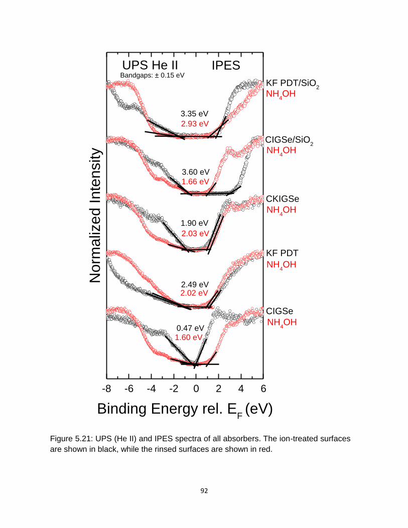
92
-8 -6 -4 -2 0 2 4 6
NH4OH
NH4OH
NH4OH
NH4OH
NH4OH
Bandgaps: 0.15 eV
3.35 eV
2.93 eV
3.60 eV
1.66 eV
1.90 eV
2.03 eV
2.49 eV2.02 eV
0.47 eV1.60 eV
No
rma
lize
d I
nte
nsity
Binding Energy rel. EF (eV)
IPESUPS He II
KF PDT/SiO2
CIGSe/SiO2
CKIGSe
KF PDT
CIGSe
Figure 5.21: UPS (He II) and IPES spectra of all absorbers. The ion-treated surfaces
are shown in black, while the rinsed surfaces are shown in red.

93
(VBMs) do not deviate much from the “pre-rinse” VBMs. The largest change is seen for
the CIGSe/SiO2 absorber, where the pre-rinse bandgap was 3.60 ± 0.15 eV and the post-
rinse 1.66 ± 0.15 eV.
5.4 – CONCLUSION
In summary, XPS, UPS, and IPES were used to investigate the chemical and electronic
properties of this alkali study. We find that the Cu:In ratio is smallest for both KF PDT
absorbers (in comparison to the large Cu peak seen for the bare CIGSe absorbers),
suggesting that the KF PDT leads to a depletion of Cu from the surface of nominally
stoichiometric films. We note that the Cu:In ratio of the bare CIGSe absorbers deposited
with constant elemental flux is much larger than the three-stage coevaporated PDIL
CIGSe absorbers, and thus a reduction of the Cu surface content can be more easily
achieved.
In-F and Ga-F species are found on the ion-treated surfaces of both KF PDT
absorbers. After the NH4OH treatment, the Ga-F and Ga-O bonds are removed, and a
Ga depletion of the surfaces is observed. In-F bonds are greatly reduced, but still present,
and the contribution of In-O species is enhanced. The Ga/(In+Ga) ratio of the CIGSe,
CKIGSe, and CIGSe/SiO2 absorbers are larger than the KF PDT absorbers. The ratio
decreases after the NH4OH treatment except for the KF PDT/SiO2 absorber where there
is an increase.
Both K and F are deposited on the surfaces of the KF PDT absorbers, and K and
F are also observed the surface of the CKIGSe film, but to a smaller degree. The NH4OH
treatment removes the K completely from the surface of KF PDT/SiO2, significantly

94
reduces K and F on KF PDT, and slightly reduces K and F for CKIGSe. Na is present on
CIGSe, KF PDT, and CKIGSe pre and post-rinse but Na is only observed for the SiO2
absorbers after the NH4OH rinse, suggesting that Na is deposited during the NH4OH
treatment. The Na on all the absorbers are found in an Na-O bonding environment.
UPS and IPES show that incorporation of K widens the bandgap of the CIGSe
absorber, with the largest surface bandgap (among the rinsed samples) of 2.93 ± 0.15 eV
found for the KF PDT/SiO2 absorbers. In future experiments (projects), it would thus be
of great interest to also determine the band alignment between such modified absorber
surfaces (with K-induced bandgap widening) and both standard (CdS) and alternative
[(Zn(O,S)] buffer materials to study the impact on the interfacial electronic structure.

95
CHAPTER SIX
ELECTRONIC STRUCTURE OF THE Zn(O,S)/CIGSe THIN-FILM SOLAR CELL
INTERFACE
The majority of the following chapter has been previously published in Progress in Photovoltaics: Research and Applications and reports work performed to study the electronic properties of alternative buffer materials. Reprinted with permission from Michelle Mezher, Rebekah Garris, Lorelle M. Mansfield, Kimberly Horsley, Lothar Weinhardt, Douglas Duncan, Monika Blum, Samantha G. Rosenberg, Marcus Bär, Kannan Ramanathan, and Clemens Heske, Electronic structure of the Zn(O,S)/CIGSe thin-film solar cell interface, Progress in Photovoltaics: Research and Applications 2016, In Print. Copyright 2016 John Wiley and Sons.
6.1 – INTRODUCTION
Cu(In,Ga)Se2 (CIGSe) thin-film photovoltaic devices have achieved a record efficiency of
22.3% on a laboratory scale4. Traditionally, high-efficiency devices contain a CdS buffer
layer between CIGSe absorber and transparent front electrode42. In contrast, the recent
breakthrough was achieved with an alternative Cd-free buffer layer [Zn(O,S)], and other
groups have also reported high conversion efficiencies for the Zn(O,S)/CIGSe
system58,130–132. Such buffers are desirable as they offer higher transparency and thus
the possibility of increasing the current collection in the shorter wavelength region. For
further optimizing such alternative buffer layers, understanding the interactions between
the chalcopyrite absorber and the buffer layer is crucial, and several studies with this
focus have already been published84,133–136.
A characteristic of record CdS/CIGSe devices is the presence of a flat conduction
band alignment at the buffer/absorber interface, both for CdS/CuInSe2 and
CdS/Cu(In,Ga)(S,Se)225,52,59. In contrast, the less efficient CdS/Cu(In,Ga)S2 system has
been shown to exhibit a cliff-like conduction band offset (CBO)51. It is thus important to

96
understand the band alignment at the Zn(O,S)/CIGSe interface by direct and independent
analysis of the valence and conduction band energies without the detrimental effects of
sputter depth-profiling, and to compare its commonalities and differences with respect to
the CdS-containing CIG(S)Se thin-film photovoltaic systems.
When using Zn(O,S) as a buffer material, it should be noted that ZnS and ZnO
have large optical band gaps, 3.54 eV137 and 3.3 eV138, respectively, whereas the band
gap of the Zn(O,S) alloy can show a strong bowing effect as the O:S ratio varies139,140,
with a minimum at 2.6 eV for a S/(S +O) ratio of 45%57. Nevertheless, even at this
minimum, Zn(O,S) still exhibits an optical band gap that is approximately 0.2 eV larger
than that of CdS (2.4 eV47), promising a higher transparency. To thus gain insights into
the electronic level alignment when utilizing Zn(O,S) buffers, it is pertinent to perform a
detailed experimental study; here, we present the first non-destructive analysis of the
interface using XPS, UPS, and IPES, investigating samples with varying buffer layer
thickness.
6.2 – EXPERIMENTAL
A Zn(O,S)/CIGSe sample series was deposited at NREL, consisting of a CIGSe “bare”
absorber and two Zn(O,S)/CIGSe interface samples of varying Zn(O,S) thickness. The
absorbers were deposited onto a Mo-coated soda lime glass substrate using the standard
three-stage process and a bulk Ga/(Ga+In) ratio of 0.318. Our surface-sensitive XPS
studies find a Ga/(Ga+In) ratio of 0.33 and 0.32 (± 0.10) for the CIGSe and thinnest buffer
layer sample, respectively. The Zn(O,S) films were grown by chemical bath deposition
(CBD) utilizing zinc sulfate, thiourea, ammonium hydroxide, and dimethyl sulfoxide141.

97
Auger depth profiling studies at NREL showed that the CBD process yielded Zn(O,S)
films with a composition of ~25 at% S and ~20 at% O (S/(S+O) ~ 0.56). The CBD time
was varied to control the thickness of the Zn(O,S) layer on the absorber – the “thick”
Zn(O,S)/CIGSe sample was deposited by the standard 22.5 minute CBD process,
whereas the “thin” Zn(O,S)/CIGSe sample was deposited by an abbreviated 5 minute
CBD. Completed twin devices demonstrated an average efficiency of 17.7% (with a
maximum of 17.8%). According to our XPS analysis, the thick layer is clearly a “closed”
layer [Chapter 7].
XPS, UPS, and IPES were performed at UNLV to investigate all three samples. XPS
measurements were taken using Mg Kα and Al Kα radiation, and He I and II irradiation
were used for the UPS measurements. In this paper, only the results obtained with Mg Kα
and He I radiation are shown (while the other results nevertheless contributed to the
overall interpretation). XPS and UPS measurements were taken with a SPECS PHOIBOS
150 MCD electron analyzer, calibrated using core-level and Auger peaks of clean Ag, Cu,
and Au foils (for XPS)78, and the Fermi energy of the Au foil (for UPS and IPES). All
samples were treated with a low-energy (50 eV) Ar+ ion treatment at a low incidence
angle. This has been shown25,83 to be very effective in removing C and O contaminants
from chalcopyrite, CdS, and ZnO surfaces without creating metallic phases commonly
found when sputter-cleaning or depth-profiling such surfaces with higher ion energies.
The CIGSe absorber was treated for a total of 120 min, and both Zn(O,S)/CIGSe samples
were treated for 20 min each to remove (a portion of) the surface adsorbates while
minimizing any potential beam damage (note that intense x-ray and electron flood gun
irradiation has been shown to induce changes in the zinc hydroxide / zinc oxide ratio of

98
hydroxide-rich films142,143). All peaks were analyzed by fitting the different spectral
intensities with Voigt functions (with coupled Lorentzian and Gaussian widths) and a
linear background using the Fityk peak-fitting program90. A commercial low-energy
electron gun (Staib) and a home-built Dose-type detector with a SrF2 window and Ar:I2
filling81 were used for IPES experiments. The valence band maximum (VBM) and
conduction band minimum (CBM) were determined by linear extrapolation of the leading
edge in the valence band (UPS) and conduction band (IPES) spectra82. The base
pressure in the chamber was <5×10⁻¹⁰ mbar.
6.3 – RESULTS AND DISCUSSION
Figure 6.1 presents Mg Kα XPS spectra of the O 1s region of the thick and thin
Zn(O,S)/CIGSe samples. The shape and broadness of the O 1s peak in both samples
indicates the presence of multiple chemical species. Indeed, a fit analysis shows that a
single Voigt peak does not give a satisfactory description, indicating that at least two
species are present. Conversely, we find that the quality of the fit achieved with two Voigt
functions for each O 1s region (with a linear background and identical Gaussian and
Lorentzian widths for all the species) is already very high, and that a third component
does not lead to a significant further improvement. Consequently, the residuals shown
below each spectrum show a statistical distribution without any evidence for additional
peaks.
Comparing the binding energies with values from literature, the two components
for both samples can be assigned to ZnO and Zn(OH)2111,144. Since the Zn(O,S) is
deposited onto the CIGSe via a wet-chemical deposition route, Zn-OH bonds are not

99
unexpected58, suggesting that the dehydrogenation of the Zn(O,S) layer is incomplete for
both the thin and thick Zn(O,S)/CIGSe samples53,139. The possibility of a sulfate species
was also taken into account since the O 1s peak location of a sulfate species and a
hydroxide species are similar. However, none of our sulfur XPS spectra show any
evidence for sulfates. Overall, our XPS, x-ray excited Auger electron spectroscopy and x-
ray emission spectroscopy results suggest the presence of up to 4 different Zn species
(associated with Zn-containing bonds similar to those in ZnO, ZnS, Zn(OH)2, and ZnSe)
[Chapter 7].
534 533 532 531 530 529
x3N
orm
aliz
ed
In
ten
sity
Binding Energy (eV)
a) Thin
b) Thick
x3
XPS Mg K
O 1s
ZnO
Zn(OH)2
ZnO
Zn(OH)2
Zn(O,S)/CIGSe
Figure 6.1: XPS detail spectra of the O 1s peak and fit (components in black, sum in
red) of a) the thin (5 min) and b) the thick (22.5 min) Zn(O,S)/CIGSe samples. The
magnified residual of each fit is also shown.

100
UPS and IPES spectra to analyze the valence (VB) and conduction band (CB),
respectively, of the bare CIGSe absorber and the thick (22.5 min) Zn(O,S) CBD buffer
layer are shown in Figure 6.2. The VBM and CBM for the bare CIGSe absorber are found
at -1.05 (±0.10) below and 0.50 (±0.15) eV above the Fermi energy, respectively. The
thus derived electronic surface band gap of 1.55 (±0.18) eV agrees well with previously
-8 -6 -4 -2 0 2 4 6
± 0.18 eV
± 0.18 eV
-2.30 eV
0.45 eV
-1.05 eV
IPESUPS - He I
Zn(O,S)
CIGSe
2.75 eV
1.55 eV
Norm
aliz
ed Inte
nsity
Binding Energy rel. EF (eV)
EF
0.50 eV
Figure 6.2: He I UPS (left) and IPES (right) spectra of the bare CIGSe absorber (bottom)
and the thick Zn(O,S)/CIGSe sample (top). VBM and CBM values determined by linear
extrapolations of the leading edges (red lines) are shown, together with the resulting
electronic surface band gaps. Error bars are ±0.10 and ±0.15 eV for the VBM and CBM
determination, respectively. A Savitzky-Golay-smoothed line is shown for the IPES
spectra as a guide to the eye.

101
measured CIGSe surface band gaps of high efficiency absorbers with Cu-poor
surfaces23,25,52,59,85,86. The VBM and CBM of the Zn(O,S) layer are found at -2.30 (±0.10)
eV and 0.45 (±0.15) eV, respectively, deriving an electronic surface band gap of 2.75
(±0.18) eV. Note that the optical (bulk) band gap of a pure Zn(O,S) alloy with a S/(S+O)
ratio of ~56% is expected to be ~2.6 (±0.10) eV57. A larger Zn(O,S) surface band gap in
our case might be due to various reasons, including the presence of Zn-OH bonds (as
shown by the O 1s spectra) and the above-mentioned presence of multiple Zn-containing
species53.
To derive a complete description of the band alignment at the interface, additional
information is needed to take into account how the band bending at the absorber surface
changes during the formation of the interface, as well as whether/how a band bending
evolves in the buffer layer (as a function of thickness). For this purpose, the thin
Zn(O,S)/CIGSe sample serves as an intermediate step in the interface formation (note
that it is not possible to derive electronic structure information from an interface by sputter
depth-profiling through the top layer due to the induced structural and chemical defects
and compositional changes associated with preferential sputtering). Deriving the band
bending changes is done by comparing the core-level peak positions of the CIGSe
absorber (Se, In, Cu) to those of the thin Zn(O,S)/CIGSe sample, as listed in Table 1
(top). The observed shifts lie between 0.03 eV and 0.10 eV and indicate a very small
upward shift [0.06 eV] of the absorber surface band edges as the interface starts to form.
In other words: the (expected) downward band bending at the absorber surface is slightly
reduced by the interface formation. This needs to be compared with the CdS/CIG(S)Se
system, where we either find a negligible impact on the band edge positions25,52,59 or a

102
small additional downward shift [unpublished]. The here-observed (small) upward shift
could have several origins, including a small change in the CIGSe surface dipole upon
becoming an interface dipole to the Zn(O,S) layer, and a possible charge transfer across
the interface to influence the space-charge region. The latter interpretation would require
that the Fermi level at the interface is not pinned.
To investigate whether/how band bending evolves in the buffer layer as a function
of thickness, the core-level binding energy differences between the thin and thick Zn(O,S)
samples (Zn, O, and S core levels) are compared, as listed in Table 1 (bottom). As the
buffer layer thickness increases, the Zn, O, and S core-level peaks from the thin
Zn(O,S)/CIGSe sample also shift toward lower BE. For a quantitative analysis, we need
to take into account that the buffer layer consists of multiple chemical species, as
discussed above. For oxygen, we thus analyze both components (i.e., the ZnO and
Zn(OH)2 species) separately in order to avoid spurious peak shifts due to a variation in
Table 6.1: Core level peak positions of the bare absorber, the thin (5 min) Zn(O,S)/CIGSe sample, and the thick (22.5 min) Zn(O,S)/CIGSe sample, as well as their relative shifts.
Core Level CIGSe BE (eV) Thin 5 min Zn(O,S) BE (eV)
Shift
Se 3d 54.33 54.30 0.03
In 3d5/2 444.78 444.68 0.10
Cu 2p3/2 932.56 932.52 0.04
Core Level Thin 5 min Zn(O,S) BE (eV)
Thick 22.5 min Zn(O,S) BE (eV)
Shift
S 2p3/2 161.91 162.12 0.21
O 1s (Zn(OH)2) 532.06 532.25 0.19
O 1s (ZnO) 530.89 531.08 0.19
Zn 2p3/2 1022.33 1022.41 0.08

103
ZnO/Zn(OH)2 ratio. For sulfur, we expect one dominant species (ZnS), and thus the S
2p3/2 binding energy is taken “as derived”. For Zn, finally, we argue that there are too
many different species overlapping within the Zn 2p3/2 peak, and thus it is not possible to
separate band bending effects from variations in relative abundance of the different
species. We therefore list the binding energy values in Tab. 6.1, but do not use them for
the band alignment determination (hence shaded gray in Tab. 6.1). Overall, we derive a
shift of 0.20 eV for the buffer layer core levels. Note that the S and O core levels all shift
in unison, suggesting that these shifts are due to band bending in the buffer layer, rather
than to chemical shifts due to an altered S/(S+O) or OH/(O+OH) ratio in the buffer layer
itself. This interpretation is corroborated by a quantitative analysis of the OH/(O+OH)
ratio, which derives values for the 5 and 22.5 min Zn(O,S) samples [Chapter 7] that are
equal within the error bars of such a determination.
The full band alignment of the Zn(O,S)/CIGSe interface, including the band
bending correction, is depicted in Figure 6.3. A small conduction band offset (CBO = 0.09
± 0.20 eV) is found, indicating that the conduction band alignment at the Zn(O,S)/CIGSe
interface is essentially flat (small spike), as in25,52,59,143. Likewise, a considerable valence
band offset (VBO = 1.15 ± 0.15 eV) is formed, creating a hole barrier and decreasing
interfacial recombination. Note that the error bars were determined as a best-faith
estimate of the Gaussian distribution around the derived value (they should not be
misinterpreted as a “box of equal probability”).
As mentioned in the introduction, we have consistently found flat conduction
alignments in optimized CIG(S)Se-based devices25,52,59, with the exception of
CdS/Cu(In,Ga)S2, for which a cliff was found51. Given the fact that the O/S ratio of the

104
Zn(O,S) layer gives an additional optimization parameter for this alternative buffer layer,
it is not necessarily to be expected that a flat conduction band alignment is found. In
particular, modeling studies have suggested that buffer/absorber interfaces are far less
sensitive towards spikes than towards cliff arrangements68–70. Nevertheless, empirical
optimization time-and-again leads to electronic level alignments that are very close to
“flat”, suggesting that such an optimized level alignment should be considered one of the
primary design criteria for constructing deliberately-tailored thin film photovoltaic devices.
Eg: 2.75 ± 0.18 eV
VBO:
± 0.15 eV ± 0.15 eV
± 0.15 eV
± 0.20 eV
± 0.10 eV ± 0.10 eV
Interface
Zn(O,S) Surface
1.05 eV
0.50 eV
2.30 eV
EF
0.45 eV 0.09 eV
1.11 eV
CIGSe Surface
0.06 eV
0.20 eV
Eg: 1.55 ± 0.18 eV
CBO:
Figure 6.3: Band alignment scheme of the Zn(O,S)/CIGSe interface. The band edge
positions at the CIGSe and Zn(O,S) surfaces are shown on the left and right,
respectively. In the center, the band alignment at the interface is shown, taking
interface-induced band bending changes at the absorber surfaces and band bending
in the buffer layer into account (as indicated by the ovals).

105
6.4 – CONCLUSION
The electronic structure of the Zn(O,S)/CIGSe interface was analyzed using x-ray, UV
and inverse photoemission. We find evidence for multiple chemical environments of
oxygen in the Zn(O,S) buffer layer, best described by ZnO and Zn(OH)2 components.
Detailed analysis of the bare CIGSe and thick Zn(O,S)/CIGSe samples, together with an
optimally chosen thin Zn(O,S) intermediate sample to monitor variations of band bending
due to interface formation and increasing buffer layer thickness, allowed for a
comprehensive and all-experimental depiction of the electronic level alignment at the
interface. We find an essentially flat conduction band alignment (small spike) and a
significant valence band offset (i.e., a hole barrier). Such a structure is expected to allow
for unobstructed electron transport across this interface, beneficial for high-efficiency thin
film solar cells.

106
CHAPTER SEVEN
SOFT X-RAY SPECTROSCOPY OF A COMPLEX HETEROJUNCTION IN HIGH-
EFFICIENCY THIN-FILM PHOTOVOLTAICS: INTERMIXING AND Zn SPECIATION
AT THE Zn(O,S)/CIGSe INTERFACE
7.1 – INTRODUCTION
Cu(In,Ga)Se2 (CIGSe) thin-film photovoltaic devices have recently achieved a world-
record efficiency of 22.3% on a laboratory scale utilizing a Zn-based buffer layer (the
20.9% world-record cell from Solar Frontier K.K. utilized Zn(O,S) as the buffer layer)4.
While CdS-based CIGSe devices have traditionally dominated the record efficiencies for
this materials class,45 other groups report high conversion efficiencies with a Zn(O,S)
buffer as well (up to 21.0 %)58,131,132,145. An understanding of the interface formation is
crucial for optimizing these buffer layers and the buffer/absorber interface. While several
studies have been published showing theoretical and experimental interfacial band
alignments,60,84,133,134,136,140 there is a need to better understand the chemical interactions
at the buffer/absorber interface, as this information can aid in deliberately tailoring the
electronic band alignment. We note that current state-of-the-art Zn(O,S)-based devices
feature a flat conduction band alignment60.
Previous studies have revealed a S/Se intermixing at the CdS/CIG(S)Se interface
of high efficiency thin film devices with a chemical bath-deposited buffer layer48–50,146.
Only few studies report on intermixing at the heterojunction between Zn(O,S) and
chalcopyrites139,147. To gain better insights into the formation of the Zn(O,S)/CIGSe buffer
layer and the chemical interactions at the interface in current state-of-the-art devices, we
employ x-ray photoelectron spectroscopy (XPS), x-ray-excited Auger electron

107
spectroscopy (XAES), and synchrotron-based soft x-ray emission spectroscopy (XES) on
Zn(O,S)/CIGSe samples with varying buffer layer thickness.
7.2 – EXPERIMENTAL
The sample set was deposited at the National Renewable Energy Laboratory (NREL). It
consists of a CIGSe bare absorber and three Zn(O,S)/CIGSe interface samples of varying
Zn(O,S) chemical bath deposition (CBD) times141. The standard three-stage process, with
a nominal Ga/(Ga+In) ratio of 0.3, was used to grow the CIGSe absorbers on Mo-
sputtered glass18. The “thick” Zn(O,S) sample was deposited using the standard 22.5 min
CBD process, and for the “thin” and “intermediate” samples, the process was interrupted
after 5 and 10 min, respectively. Completed twin devices showed an average conversion
efficiency of 17.7%. The CBD process yielded Zn(O,S) buffer films with a S/(S+O) ratio
of ~0.56, as derived by Auger depth profiling studies conducted at NREL.
XPS and XAES were conducted at UNLV, while XES was performed at the
Advanced Light Source (ALS), Lawrence Berkeley National Laboratory. XPS
measurements were taken using Mg and Al Kα radiation with a SPECS PHOIBOS 150
MCD electron analyzer and calibrated using the Auger and core-level peaks of clean Cu,
Ag, and Au foils80. The XES spectra were taken at the SALSA endstation101 on beamline
8.0.1 at the ALS, utilizing the variable line-space grating (VLS) spectrometer. The spectra
were calibrated using the prominent emission features of CdS108. The base pressure for
the XPS and XES measurements were <5x10⁻¹⁰ and <1x10⁻⁹ mbar, respectively.
The samples were briefly air-exposed (less than 5 min) before being packaged in
a vacuum-sealed container. At UNLV, the samples were immediately introduced into an

108
inert gas-filled glovebox, mounted on a sample holder, and transferred into the ultra-high
vacuum system. The samples were measured “as-received” and also after a low-energy
(50 eV) Ar+ ion treatment (two subsequent 60 min treatments for CIGSe, and three
subsequent 20 min treatments for each of the 5 and 22.5 min absorbers) at low incidence
angle, which has been shown to be effective in (partially) removing adsorbates from
chalcopyrites, ZnO, and CdS surfaces without creating metallic phases often found with
higher ion energies25,83. XPS peaks were analyzed by fitting with Voigt functions, coupled
Gaussian and Lorentzian widths, and a linear background using the Fityk Peak Fitting
Program90. For quantification, inelastic mean free paths (IMFPs) were determined by the
QUASES software148.
7.3 – RESULTS AND DISCUSSION
XPS survey spectra of the bare CIGSe absorber and the 5 and 22.5 min Zn(O,S)/CIGSe
samples are shown in Figure 7.1. The respective “as-received” spectra are shown in
black, while the “ion-treated” spectra are shown in red. The pertinent CIGSe and Zn(O,S)
photoemission and Auger lines (of Cu, In, Ga, Se, Zn, O, and S), as well as the Na lines
are labeled, in addition to the adsorbate peak associated with C. For the as-received
CIGSe absorber, the O 1s peak is particularly pronounced, especially when the
photoionization cross section is taken into account149,150. Due to the presence of this
adsorbate layer, all high-binding energy peaks in the survey spectrum (e.g., Ga 2p, Cu
2p, In MNN, Zn 2p) are suppressed in intensity. The low-energy ion treatment removes
the majority of the adsorbate species, as well as most of the Na surface species, and thus
the surface-sensitive peaks mentioned above gain in intensity. The CIGSe absorber was

109
treated for a total of 120 min, and the Zn(O,S)/CIGSe samples were treated for a total of
60 min in several steps. In Fig. 7.1 and the subsequent analysis, data after the first 20
min treatment is shown/used in order to minimize ion beam influences. In fact, as will be
discussed later, the two subsequent ion treatments of the Zn(O,S)/CIGSe samples
induced signs of surface alteration (dehydrogenation). This indicates that Zn(O,S) is more
susceptible to low-energy ion treatments (and other irradiation) than the CIGSe absorber,
CdS, or ZnO25,83,142,143. As the Zn(O,S) thickness is increased, Fig. 1 shows that all peaks
from the CIGSe absorber surface are attenuated, as expected. Small CIGSe-related core-
level peaks are detected in the spectra of the thin Zn(O,S)/CIGSe sample (e.g., the In 3d
and Se 3d peaks in Fig. 1, center). In contrast, the 22.5 min Zn(O,S) sample shows no
evidence of absorber-related peaks, suggesting that it is a continuous layer.
1200 1000 800 600 400 200 0
Se 3p
Ga 2s
Inte
nsity (
a.u
.)
Binding Energy (eV)
In M
NN In 3d
In 3s
In 3pCu 2p
Na 1s
Ga 2p
C K
VV
XPS Mg K
Zn 2p
O KLL
O 1s
S LMM
Na KLL
Se 3s
S 2s
Cu LMM
C 1s
In 4
d/G
a 3
d
Se 3d
Se 3p
S 2p
Ga LMM
Zn 3d
Zn 3p
Zn 3s
Zn LMM
Ion-Treated
Ion-Treated
Ion-Treated
22.5 min
Zn(O,S)/CIGSe
CIGSe
5 min
Zn(O,S)/CIGSe
Figure 7.1: XPS survey spectra of the untreated (black) and ion-treated (red)
Zn(O,S)/CIGSe sample series: CIGSe bare absorber (bottom), 5 min Zn(O,S) (center),
and 22.5 min Zn(O,S) (top).

110
The Na peak intensity for the CIGSe bare absorber decreases with ion treatment,
in parallel to a reduction of the oxygen and carbon signals [we note that the carbon signal
for the Zn(O,S) layers is quite sizable, which we assign to an incorporation during the
1073 1072 1071 1070988
989
990
991
992
993
994
995
996
0 min
60 min
2061
2062
2063
2064
2065
Na2S
2O
n Na
2SO
3Na
2CO
3
Na2SO
4 NaOOCH NaHCO
3
2066
Na2SeO
3
Na2C
2O
4
Na K
L2,3L
2,3
Kin
etic E
nerg
y (
eV
)
Na 1s Binding Energy (eV)
Na
Na2O
120 min
'
Figure 7.2: Modified Auger Parameter plot of Na 1s is shown before (red dot) and after different 50 eV Ar+-ion energy treatment steps (red triangles) in comparison to references (111,112) in black (error bars are ±0.05 eV on both axes). .

111
CBD process]. To gain further insight into the chemical state of Na on the CIGSe surface
and the cause of this intensity decrease, the modified Auger parameters α’ of Na were
calculated. Figure 7.2 shows the Wagner plot116 for the CIGSe absorber surface (red, ion-
treatment times as indicated), along with relevant references (black)111. The modified
Auger parameter is calculated by summing the binding energy of the Na 1s core level and
the kinetic energy of the KL2,3L2,3 Auger peak, and information about the chemical state
is gained by comparing with reference data116 along three axes: the Na 1s binding energy
(abscissa), the Na KLL kinetic energy (ordinate), and α’ (diagonal and right ordinate). The
location of the CIGSe data on the Wagner plot is indicative of Na in an oxidized chemical
environment. It is clearly different from metallic Na, but close to a large variety of O and/or
C containing Na compounds. Thus, upon ion treatment, Na is likely to be desorbed along
with the surface adsorbates. Based on earlier studies,35–38 this is not unexpected for air-
exposed CIGSe surfaces and also assumed to happen in the chemical bath solution.
Core-level peaks from the CIGSe absorber can be detected in the spectra of the
thin Zn(O,S)/CIGSe sample, indicating that the 5 min CBD of Zn(O,S) results in a layer
that is inhomogeneous and/or thinner than the region from which XPS information can be
derived (note that XPS signals are governed by an exponential attenuation function, not
a “box” function associated with a specific information depth). The absorber peaks
detected for Cu, In, and Ga are of low intensity, while, in comparison, the Se 3d peak is
larger, indicating the possibility of Se diffusion into the Zn(O,S) layer, as will be discussed
now. For the purpose of studying Se diffusion at this interface, we also include the
Zn(O,S)/CIGSe sample of intermediate thickness (10 min CBD). Figure 7.3 shows XPS
spectra of the Se 3d peak (left) and the Ga 3d/In 4d peak (right) for the CIGSe bare

112
absorber and the Zn(O,S)/CIGSe samples of increasing thickness. Due to their similar
kinetic energies, the Se 3d, Ga 3d, and In 4d peaks are expected to have similar inelastic
mean free paths (IMFPs), allowing the attenuation factors of these peaks to be compared
as an initial step. The Se peak is strongly attenuated as the Zn(O,S) CBD time increases,
but nevertheless it is still detectable even after the standard deposition time of 22.5 min.
In contrast, the peaks of the 10 min Zn(O,S)/CIGSe and 22.5 min Zn(O,S)/CIGSe
samples are extremely small (if present at all), even when magnified 100x (note that the
59 58 57 56 55 54 53 52 51 22 21 20 19 18 17 16 15
No
rma
lize
d I
nte
nsity
Binding Energy (eV)
Se 3dXPS Mg K
22.5 min Zn(O,S)
10 min Zn(O,S)
5 min Zn(O,S)
CIGSe
(x6)
(x75)
(x75)
In 4dCIGSe
22.5 min Zn(O,S)
(x100)
(x100)
10 min Zn(O,S)
5 min Zn(O,S)(x8)
Ga 3d / In 4d
Ga 3d
Figure 7.3: Mg Kα XPS spectra of the Se 3d peak (left) and the Ga 3d/In 4d region
(right) for the CIGSe bare absorber and Zn(O,S)/CIGSe samples of varying
thickness. To describe the 10 and 22.5 min spectra, the result of a fit with the CIGSe
lineshape and a linear background is shown. Multiplication factors are shown in
parentheses.

113
Ga 3d/In 4d peaks lie on the onset of the O 2s peak, at ~ 26 eV, giving rise to the steep
background observed for the 10 and 22.5 min sample). The detection of a Se signal even
after 22.5 min of Zn(O,S) CBD suggests an outdiffusion of Se during the CBD process,
similar to the CdS/CIGSe and CdS/CIGSSe interfaces48–50. All other core-level and
Auger peaks (not shown) were analyzed in a similar fashion, but no peaks were visible
for the 10 min and 22.5 min Zn(O,S) CBD sample (but note that these peaks might be
governed by shorter attenuation lengths due to their lower kinetic energy and will be
discussed in greater detail below).
In order to analyze the possibility of Se, Ga, and/or In diffusion more quantitatively,
Figure 7.4 presents an “effective Zn(O,S) layer thickness” as a function of the Zn(O,S)
CBD time. The nominal thickness values (determined by Scanning Electron Microscopy
at NREL) are shown as black data points and a line, while the effective thicknesses
derived from the Se 3d, Ga 3d, and In 4d intensity attenuation are plotted in color and
labeled (red, green and pink colors: Ga 3d/In 4d, blue: Se 3d). If there is no diffusion of
the element in question, the effective layer thickness should be similar to the nominal
thickness, while it is expected to be lower in the case of diffusion into the buffer layer. The
effective thickness derived for a given peak is calculated using
deff = λ ln(I0 / I). (7.1)
The IMFP is represented by λ, I0 is the peak intensity in the bare absorber, and I is
the peak intensity in the corresponding Zn(O,S)/CIGSe sample. We find that the Se 3d-
based effective layer thickness lies significantly below the nominal thickness line, even
when taking the error bars into account. Thus, the attenuation of the Se signal is lower
than expected, suggesting that Se is diffusing into the buffer layer during the CBD

114
process. In contrast, for the 5 min sample, the Ga 3d and In 4d effective thicknesses are
larger and on (Ga) or very close (In) to the nominal line. For the 10 min sample, we note
0 5 10 15 20 25
0
5
10
15
20
25
30
Zn(O,S) Nominal
Thickness
In 4d
Effective Z
n(O
,S)
Layer
Thic
kness (
nm
)
Deposition Time (min)
Se 3dGa 3d
Ga 3d/In 4d
Figure 7.4: Effective Zn(O,S) layer thickness derived from Se 3d (blue), Ga 3d (red,
5 min), In 4d (green, 5 min), Ga 3d/In 4d combined (pink, 10 min) and nominal
thickness (black) as a function of Zn(O,S) CBD time. The 10 min nominal thickness
and Ga 3d/In 4d data were shifted slightly along the abscissa to differentiate between
the data points.

115
that the Ga 3d/In 4d region also includes the Mg Kβ excitation of the O 2s line, which
would give rise to a satellite approximately 9 eV lower than the O 2s peak (~17 eV), and/or
contributions from inelastically scattered Zn 3d electrons (peak at ~10 eV). Nevertheless,
because the peak in the Ga 3d/In 4d region is clearly present for the 10 min sample, we
show the effective layer thickness based on the attenuation of the combined Ga 3d/In 4d
peak (pink), ignoring possible O 2s or Zn 3d are contributions (leading to a large and
asymmetric error bar). The effective layer thickness is again close to the nominal
thickness line, suggesting that there is no significant diffusion of In or Ga into the buffer.
22 21 20 19 18 17 16
x2
5 min
Zn(O,S)
Ga 3d/In 4d
Binding Energy (eV)
x5
In 4d
XPS Mg K
CIGSe
Ga 3d
In 4d
Ga 3d
No
rmaliz
ed Inte
nsity
Figure 7.5: XPS detail spectra of the Ga 3d/In 4d region of the CIGSe absorber
(bottom) and 5 min Zn(O,S) (top). Fit curves for In:Ga contributions to the peak are
shown along with their respective residuals (purple).

116
For the 22.5 min sample, we argue that there is no detectable Ga 3d/In 4d peak, noting
the absence of the (normally dominant) In 3d5/2 peak. The finding of a Se outdiffusion into
the Zn(O,S) buffer layer is reminiscent of the CdS/CIGSe interface, in which a pronounced
S-Se exchange at the interface is found48–50. In the present case of a Zn(O,S) buffer, the
diffusion of Se into the buffer layer leads us to speculate that it is most likely in a Zn-Se
bonding environment.
Figure 7.5 shows fits of the Ga 3d/In 4d peaks of the bare CIGSe absorber and the
5 min Zn(O,S) sample in order to see if the Ga/(Ga+In) ratio at the absorber surface
changes with the addition of the buffer layer. The peaks were fit with a linear background
and Voigt profiles, using coupled Gaussian widths for all components, and coupled but
separate Lorentzian widths for In and Ga, respectively. The ratios of the spin-orbit split
peaks were fixed according to their multiplicity, along with their respective peak
separation, 0.86 eV for In113,114 and 0.46 eV for Ga115. The data is shown with black dots,
the In 4d components in green, the Ga 3d components in blue, and the resulting fit in red.
The residual of the fit is shown below each spectrum (purple). We note that these shallow
core levels already possess some band character, and thus the quality of the fit is very
surprisingly high, especially given all the above-mentioned boundary conditions included
in the fit. The surface Ga/(Ga+In) ratio for the CIGSe absorber and 5 min Zn(O,S)/CIGSe
samples are 0.33 and 0.32 (± 0.10), respectively, indicating no change in the surface ratio
with the addition of the buffer layer. Having thus gained a detailed description of the
absorber surface, we can now take a closer look at the overlayer and its contributions to
the interface formation.

117
As mentioned previously, the 5 and 22.5 min Zn(O,S)/CIGSe samples were ion
treated in three 20 min increments. Figure 7.6 (left) shows XPS spectra of the 22.5 min
Zn(O,S)/CIGSe O 1s peak as a function of ion treatment time. The purpose of the low
energy ion treatment is to remove surface adsorbates without creating metallic species
at the surface. Indeed, we see that with the 20 min treatment, the O peak is reduced
(partial removal of adsorbates) and the main peak position is identical to the untreated
surface. However, with each subsequent treatment, the peak shifts toward lower BE and
536 534 532 530 528
60 min
40 min
No
rmaliz
ed Inte
nsity
Binding Energy (eV)
0 min
20 min H2O
ZnO
x2
0 min
O 1s
XPS Mg K
Zn(OH)2
ZnO
Zn(OH)2
x3
ZnOZnO
Zn(OH)2
x2
60 min
Zn(OH)2
Thick Zn(O,S) 20 min
x2
40 min
Figure 7.6: (Left) XPS spectra of the 22.5 min Zn(O,S) O 1s peak as a function of ion
treatment time. (Right) Fits of the O 1s peak show a change in OH/(OH+O) ratio as a
function of ion treatment time.

118
the shape changes as well. This is also true for the Zn and S peaks (not shown): the
untreated and 20 min treated surface peak positions are identical, and with each
subsequent treatment, the peak shifts to lower BE. The broadness and shape of the O
1s peak suggest that there are multiple chemical species of O in the (untreated) Zn(O,S)
film. On the right of Figure 7.6, a fit analysis of the peak (as a function of ion treatment)
shows that at least three species are present at the untreated surface, and at least two O
species after each treatment. The peaks were normalized to peak height in order to easily
visualize changes in peak component ratios. The peaks were fit with a linear background,
identical Gaussian and Lorentzian widths, and fixed positions for all species. The
residuals shown below the spectra indicate that the quality of the fit is quite high for the
ion-treated surfaces. In contrast, the untreated O 1s peak shows a characteristic
oscillation, which can be reduced by decoupling the Lorentzian width of this fit from that
of the other three spectra. We thus derive that the spectrum of the untreated surface is a
convolution of at least three species. Because there is a reduction in the O 1s peak
intensity with the first ion treatment step, we believe that such additional species need to
be ascribed to surface adsorbates. Based on their binding energies, the three
components for the untreated peak are assigned to H2O, Zn(OH)2, and ZnO111,112. For
the treated peaks, the components are assigned to Zn(OH)2 and ZnO only. The presence
of Zn(OH)2 suggests that the dehydrogenation of the Zn(O,S) layer during deposition is
incomplete, indicating that a better description of this layer would be “Zn(O,OH,S)”. Also,
it cannot be ruled out that Zn(OH)2 might be formed at the surface during the (brief) air
exposure. The fits of the O 1s peaks show that, with increasing ion treatment time, the
OH/(O+OH) ratio changes - a reduction in Zn(OH)2 and an increase in ZnO suggests that

119
the Zn(O,S) surface is more susceptible to the low-energy ion treatment than, e.g., the
ZnO surface commonly used as a window layer CIGSe devices. This beam-induced
dehydrogenation is not unexpected, as similar results have been found utilizing intense
x-rays and electron flood gun irradiation on Zn(OH)2-rich samples142,143. Nevertheless, we
use data from the 20 min ion treatment for our analysis because this surface represents
the best compromise between reduced contributions from surface adsorbates and
minimal ion beam damage.
The Zn 2p3/2 and S 2p/Se 3p spectra for the 5 and 22.5 min Zn(O,S)/CIGSe
samples are shown in Figure 7.7, along with the binding energy markers for several
1028 1026 1024 1022 1020 1018 170 168 166 164 162 160 158 156
No
rma
lize
d I
nte
nsity
Binding Energy (eV)
Zn 2p3/2
ZnSe
ZnSZn(OH)
2
ZnOZn(SO
4)
22.5 min
5 min
Zn(SO4) ZnS
XPS Mg K
22.5 min
5 min
Se 3p
S 2p
Figures 7.7: XPS spectra of the Zn 2p3/2 peak (left) and S 2p/Se 3p peaks (right) for
the 5 and 22.5 min Zn(O,S) samples. Reference peak positions (111,112) are indicated
above both peaks.

120
references111,112. Because the binding energies of the Zn references overlap (left), and
because the observed peak is rather broad, it does not allow for an unambiguous
assignment of the different species. This is not necessarily surprising – so far, our analysis
has suggested three bonding partners for Zn, namely O and OH from the O 1s peak fit
and Se from the diffusion analysis. Furthermore, bonding to sulfur is also expected for the
Zn(O,S) film surfaces. The S 2p/Se 3p spectra (right) show (a) the presence of sulfur in
a sulfide environment, as expected, (b) the presence of Se for the 5 min samples (as
discussed above; note that the Se 3p peak is much weaker than the Se 3d peak, and
hence it is not seen for the 22.5 min sample), and (c) no evidence for sulfates on the
surface.
XES spectra of the S L2,3 and Se M2,3 emission as a function of Zn(O,S) CBD time,
excited non-resonantly with a photon energy of 180 eV, are presented in Figure 7.8. The
CIGSe spectrum shows the Se M2,3 emission, while the Zn(O,S)/CIGSe samples are
dominated by S L2,3 emission. The magnification factors at the right hand side of each
spectrum show that the Se M2,3 is significantly weaker than the S L2,3 emission. The
intensity differences between the Se M2,3 and S L2,3 emission is due to the difference in
fluorescence yield for the S 3s to S 2p transition (S L2,3) and the Se 4s to Se 3p transition
(Se M2,3). As the Zn(O,S) layer is deposited, the characteristic spectrum of ZnS emerges.
In particular, the two features at ~151.2 and ~152.4 eV (in the ZnS reference) are
associated with electrons from the Zn 3d-derived band decaying into the S 2p1/2 and S
2p3/2 core holes. We do note that the Zn 3d-derived features are slightly shifted towards
lower emission energies (by ~0.2 eV), indicating a different Zn chemical environment due
to the presence of multiple Zn species (ZnS, ZnSe, Zn(OH)2, and ZnO). There is no

121
evidence of sulfates, as seen by the lack of a dominant peak at ~161 eV,143,151 in contrast
to a photoinduced sulfate formation observed for ILGAR-Zn(O,OH)/CIGSSe143,151.
To gain insights into the component(s) contributing to the 5 min and 10 min spectra,
the 22.5 min spectrum (i.e., the S L2,3 emission of the Zn(O,S) overlayer) was subtracted
after normalizing all spectra to overall peak area. The resulting difference spectra are
presented in Figure 7.9-a (bottom). The 5 min difference (red) and the 10 min difference
(blue) both show a dip at ~147.5 eV and a maximum at 150 eV, which we interpret as a
144 148 152 156 160 164
No
rma
lize
d I
nte
nsity
S L2,3
(x40)
(x1.3)
Emission Energy (eV)
(x3)
CIGSe
ZnS Ref.
22.5 min
10 min
5 min
Se M2,3
XESh
exc. 180 eV
"Zn 3d"
Figure 7.8: S L2,3 and Se M2,3 emission of the Zn(O,S)/CIGSe interface as a function of
CBD time and a ZnS reference. Multiplication factors are shown in parentheses.

122
spectral-weight shift of the main S L2,3 peak. Comparison with reference compounds
(Ga2S3, In2S3, CuInS2, CuS, Cu2S, and Zn(O,S), Figure 7.9-b) suggests that this could be
indicative for a different chemical environment of the sulfur atoms near the substrate.
Furthermore, we observe a maximum at ~ 153.5 eV; at this energy, Ga2S3, In2S3, and
CuInS2 all exhibit additional partial density of states. A strong contribution of S-Cu bonds
can, however, likely be ruled out due to the absence of any spectral difference at ~ 159
eV (i.e., the region of the Cu 3d contributions in CuInS2 and the Cu sulfides). The
144 146 148 150 152 154 156 158 160
Cu2S
CuS
b)
(5 min-22.5 min)x20
In2S
3
Ga2S
3
CuInS
No
rma
lize
d I
nte
nsity
Emission Energy (eV)
Zn(O,S)
(10 min-22.5 min)x30
XES
S L2,3
hexcit.
= 180 eV
a)
Figure 7.9: a) Difference spectra from subtracting the 22.5 min Zn(O,S) S L2,3 emission
from the 5 min (red) and 10 min(blue) spectra. b) Reference spectra for comparison.

123
difference spectra thus suggest that, in addition to the Zn-S bonding environment in the
Zn(O,S) buffer layer, additional S chemical bonding environments are present at the
interface to the CIGSe absorber, most likely in an S-In and/or S-Ga bonding environment,
similar to what has been previously observed for the CdS/CIGSe interface48.
7.4 – CONCLUSION
The Zn(O,S)/CIGSe interface has been investigated using XPS, XAES, and XES to
investigate the chemical structure. Detailed analysis of the bare CIGSe absorber and
Zn(O,S)/CIGSe samples of varying CBD times allowed for a comprehensive analysis of
the chemical interactions at this interface. We find evidence for an upward diffusion of Se
into the buffer layer, most likely in a Zn-Se environment, and intermixing of S at the
interface, most likely in a S-Ga and/or S-In environment. We find multiple chemical
environments of Zn, best described by ZnO, Zn(OH)2, ZnS, and ZnSe. There is no
evidence for sulfates in the Zn(O,S) layer (photoinduced or otherwise), but we do find
evidence for Ar+ ion beam-induced dehydrogenation of the Zn(O,S) layer. The resulting
chemical interactions during the Zn(O,S)/CIGSe interface formation are found to be quite
similar to those at the CdS/CIGSe interface48–50 but feature a higher degree of complexity
with respect to the local chemical environment of the group II component.

124
CHAPTER EIGHT
SUMMARY
In this dissertation, the impact of novel deposition parameters on both industry-
manufactured and lab-based chalcopyrites are investigated and presented. The two new
“hot topics” of the chalcopyrite photovoltaic field include the use of KF post-deposition
treatments and alternative buffer layers. To provide insight on these novel pathways to
high efficiency CIGSe devices, XPS, UPS, IPES, as well as XES and XAES are utilized
to investigate multiple sample sets designed to create a thorough approach that offers
insight on the electronic and chemical structures of the treated absorbers and/or the
absorber/buffer interface. The purpose of this is to aid in the further optimization of high
efficiency CIGSe thin-film photovoltaics.
Chapters 4 and 5 explore the effects of the first “hot topic”, alkali-treatments, on
CIGSe absorbers. The absorbers presented in Chapter 4 were taken from the production
line of STION and the National Renewable Energy Laboratory. In general, the alkali-
treatments on these absorbers are shown to partially remove surface adsorbates, change
the surface Cu:In (STION and NREL), Se:In (STION and NREL), and Ga/(Ga+In) ratios
(NREL). The treatments deposit K, F, and/or Na on the surface and changes to the S/Se
ratios are seen for the STION absorbers. Alkali-treatments change the VBM position and
large differences are found between high efficiency KF samples and low efficiency KF
samples. This indicates the KF-treatment process does not affect the substrate
homogenously. While trends were similar within the STION and NREL absorber sets
separately, the alkali-treatments do not affect the STION and NREL absorbers the same.
Chapter 5 investigates effects of KF treatments when incorporated utilizing

125
different deposition techniques and SiO2 barriers deposited on the soda-lime glass. We
find that the Cu:In ratio is smallest for both KF PDT suggesting that the KF PDT leads to
a depletion of Cu from the surface of nominally stoichiometric films. Both K and F are
deposited on the surfaces of the KF PDT absorbers, and K and F are also observed the
surface of the CKIGSe film, but to a smaller degree. In-F and Ga-F species are found on
the ion-treated surfaces of both KF PDT absorbers. After the NH4OH treatment, the Ga-
F and Ga-O bonds are removed, and a Ga depletion of the surfaces is observed. In-F
bonds are greatly reduced, but still present, and the contribution of In-O species is
enhanced. The NH4OH treatment also removes the K completely from the surface of KF
PDT/SiO2, significantly reduces K and F on KF PDT, and slightly reduces K and F for
CKIGSe. Na is present on CIGSe, KF PDT, and CKIGSe pre and post-rinse but Na is
only observed for the SiO2 absorbers after the NH4OH rinse, suggesting that Na is
deposited during the NH4OH treatment. The Na on all the absorbers are found in an Na-
O bonding environment. UPS and IPES show that incorporation of K widens the bandgap
of the CIGSe absorber, with the largest surface bandgap (among the rinsed samples) of
2.93 ± 0.15 eV found for the KF PDT/SiO2 absorbers.
The second “hot topic” leading to high efficiency and world-record CIGSe devices
is the use of alternative buffer layers, most notable Zn(O,S), a material offering the
possibility of increasing the current collection in the shorter wavelength region of the solar
spectrum. To further optimize these photovoltaic devices, an understanding of the
interactions between the absorber and the buffer layer is crucial and this investigation is
presented in Chapters 6 and 7. Chapter 6 presents the electronic structure of the
Zn(O,S)/CIGSe interface utilizing XPS to monitor variations of band bending due to

126
interface formation and increasing buffer layer thickness, UPS to measure the valence
band maximums, and IPES to measure the conduction band minimums of the samples.
The interfacial band alignment features an essentially flat conduction band offset (0.09 ±
0.20 eV) and a significant valence band offset (1.11 ± 0.15 eV) acting as a hole barrier.
Such an alignment allows for unobstructed electron transport and limits the interfacial
recombination, beneficial for high-efficiency thin film solar cells. In addition to the band
alignment, multiple chemical environments for O are found in the Zn(O,S) buffer layer
best described by ZnO and Zn(OH)2 components, further investigated in Chapter 7.
Chapter 7 presents the chemical structure of the Zn(O,S)/CIGSe interface with
evidence for the diffusion of Se upward into the buffer layer, most likely in a Zn-Se bonding
environment. S also intermixes at the interface, most likely creating Ga-S and/or In-S
species. With the interfacial intermixing, evidence indicates multiple bonding
environments of Zn, best described by ZnO, Zn(OH)2, ZnS, and ZnSe. Overall, the
resulting chemical interactions at the Zn(O,S)/CIGSe interface are very similar to the
chemical interactions at the CdS/CIGSe interface.
127
APPENDIX
LIST OF ABBREVIATIONS AND SYMBOLS
α' Modified Auger Parameter
ACS American Chemical Society
ALS Advanced Light Source
AM 1.5 Air-mass 1.5
B Boron
BE Binding energy
CB Conduction band
CBD Chemical bath deposition
CBM Conduction band maximum
CdS Cadmium Sulfide
CdTe Cadmium Telluride
CIGSe Cu(In1-xGax)Se2
CIGSSe Cu(In1-xGax)(S,Se)2
DI De-ionized
EF Fermi level
Eg Band gap
Evac Vacuum level
FAT Fixed Analyzer Transmission
FWHM Full width at half maximum
HOPE Hands on Photovoltaic Experience
hν Photon energy
ILGAR Ion laser gas reaction
IMFP Inelastic Mean Free Path
IPES Inverse Photoemission Spectroscopy
KE Kinetic energy
KF Potassium Fluoride
NaF Sodium Fluoride
NREL National Renewable Energy Laboratory

128
ODC Ordered defect compound
PDIL Process development and integration laboratory
PDT Post-deposition treatment
PV Photovoltaic
PVD Physical Vapor Deposition
Si Silicon
SURE Summer Undergraduate Research Experience
TCO Transparent conductive oxide
UHV Ultra-high Vacuum
UPS Ultra-violet Photoelectron Spectroscopy
VB Valence band
VBM Valence band maximum
Φ Work Function
XAES X-ray Auger Electron Spectroscopy
XES X-ray Emission Spectroscopy
XPS X-ray Photoelectron Spectroscopy
ZnO Zinc Oxide
Zn(OH2) Zinc Hydroxide
Zn(O,S) Zinc Oxysulfide
ZnS Zinc Sulfide
ZnSe Zinc Selenide

129
REFERENCES
(1) This Month in Physics History
http://www.aps.org/publications/apsnews/200904/physicshistory.cfm (accessed
Oct 21, 2015).
(2) Green, M. A.; Emery, K.; Hishikawa, Y.; Warta, W.; Dunlop, E. D. Solar Cell
Efficiency Tables (Version 46). Prog. Photovolt. Res. Appl. 2015, 23 (7), 805–812.
(3) Shay, J. L.; Wagner, S.; Kasper, H. M. Efficient CuInSe2/CdS Solar Cells. Appl.
Phys. Lett. 1975, 27 (2), 89–90.
(4) http://www.solar-frontier.com/eng/news/2015/C051171.html (accessed Dec 10,
2015).
(5) Shockley, W.; Queisser, H. J. Detailed Balance Limit of Efficiency of P‐n Junction
Solar Cells. J. Appl. Phys. 1961, 32 (3), 510–519.
(6) Vos, A. D. Detailed Balance Limit of the Efficiency of Tandem Solar Cells. J. Phys.
Appl. Phys. 1980, 13 (5), 839.
(7) Pierret, RF. Semiconductor Device Fundamentals 2nd Edition
(8) Repins, I.; Contreras, M. A.; Egaas, B.; DeHart, C.; Scharf, J.; Perkins, C. L.; To,
B.; Noufi, R. 19·9%-Efficient ZnO/CdS/CuInGaSe2 Solar Cell with 81·2% Fill
Factor. Prog. Photovolt. Res. Appl. 2008, 16 (3), 235–239.
(9) Kaufmann, C. A.; Neisser, A.; Klenk, R.; Scheer, R. Transfer of Cu(In,Ga)Se2 Thin
Film Solar Cells to Flexible Substrates Using an in Situ Process Control. Thin
Solid Films 2005, 480–481, 515–519.
(10) Chirilă, A.; Reinhard, P.; Pianezzi, F.; Bloesch, P.; Uhl, A. R.; Fella, C.; Kranz, L.;
Keller, D.; Gretener, C.; Hagendorfer, H.; Jaeger, D.; Erni, R.; Nishiwaki, S.;
Buecheler, S.; Tiwari, A. N. Potassium-Induced Surface Modification of
Cu(In,Ga)Se2 Thin Films for High-Efficiency Solar Cells. Nat. Mater. 2013, 12
(12), 1107–1111.
(11) Caballero, R.; Kaufmann, C. A.; Eisenbarth, T.; Unold, T.; Klenk, R.; Schock, H.-
W. High Efficiency Low Temperature Grown Cu(In,Ga)Se2 Thin Film Solar Cells
on Flexible Substrates Using NaF Precursor Layers. Prog. Photovolt. Res. Appl.
2011, 19 (5), 547–551.
(12) Nishiwaki, S.; Kohara, N.; Negami, T.; Wada, T. MoSe2 Layer Formation at
Cu(In,Ga)Se 2/Mo Interfaces in High Efficiency Cu(In1- xGax)Se2 Solar Cells. Jpn.
J. Appl. Phys. 1998, 37 (Part 2, No. 1A/B), L71–L73.
(13) Bär, M.; Weinhardt, L.; Heske, C.; Nishiwaki, S.; Shafarman, W. N. Chemical
Structures of the Cu(In,Ga)Se2/Mo and Cu(In,Ga)(S,Se)2 /Mo Interfaces. Phys.
Rev. B 2008, 78 (7), 75404.
(14) Weinhardt, L.; Blum, M.; Bär, M.; Heske, C.; Fuchs, O.; Umbach, E.; Denlinger, J.
D.; Ramanathan, K.; Noufi, R. Chemical Properties of the Cu(In,Ga)Se2/Mo/glass
Interfaces in Thin Film Solar Cells. Thin Solid Films 2007, 515 (15), 6119–6122.

130
(15) Bär, M.; Nishiwaki, S.; Weinhardt, L.; Pookpanratana, S.; Shafarman, W. N.;
Heske, C. Electronic Level Alignment at the Deeply Buried absorber/Mo Interface
in Chalcopyrite-Based Thin Film Solar Cells. Appl. Phys. Lett. 2008, 93 (4),
42110-042110–042113.
(16) Pettersson, J.; Törndahl, T.; Platzer-Björkman, C.; Hultqvist, A.; Edoff, M. The
Influence of Absorber Thickness on Cu(In,Ga)Se2 Solar Cells With Different Buffer
Layers. IEEE J. Photovolt. 2013, 3 (4), 1376–1382.
(17) Gloeckler, M.; Sites, J. R. Potential of Submicrometer Thickness Cu(In ,Ga)Se2
Solar Cells. J. Appl. Phys. 2005, 98, 103703–103703.
(18) Contreras, M. A.; Egaas, B.; Ramanathan, K.; Hiltner, J.; Swartzlander, A.;
Hasoon, F.; Noufi, R. Progress toward 20% Efficiency in Cu(In,Ga)Se2
Polycrystalline Thin-Film Solar Cells. Prog. Photovolt. Res. Appl. 1999, 7 (4),
311–316.
(19) https://www.researchgate.net/figure/277695065_fig3_Figure-75-Sketch-of-the-
three-stage-process-Values-are-given-for-information (accessed May 9, 2016).
(20) Markvart, T.; Castañer, L. Practical Handbook of Photovoltaics: Fundamentals
and Applications; Elsevier, 2003.
(21) Contreras, M. A.; Tuttle, J.; Gabor, A.; Tennant, A.; Ramanathan, K.; Asher, S.;
Franz, A.; Keane, J.; Wang, L.; Scofield, J.; Noufi, R. High Efficiency
Cu(In,Ga)Se2-Based Solar Cells: Processing of Novel Absorber Structures. In
IEEE Photovoltaic Specialists Conference - 1994; Vol. 1, pp 68–75 vol.1.
(22) Kemell, M.; Ritala, M.; Leskelä, M. Thin Film Deposition Methods for CuInSe2
Solar Cells. Crit. Rev. Solid State Mater. Sci. 2005, 30 (1), 1–31.
(23) Bär, M.; Nishiwaki, S.; Weinhardt, L.; Pookpanratana, S.; Fuchs, O.; Blum, M.;
Yang, W.; Denlinger, J. D.; Shafarman, W. N.; Heske, C. Depth-Resolved Band
Gap in Cu(In,Ga)(S,Se)2 Thin Films. Appl. Phys. Lett. 2008, 93 (24), 244103-
244103–3.
(24) Schmid, D.; Ruckh, M.; Grunwald, F.; Schock, H. W. Chalcopyrite/defect
Chalcopyrite Heterojunctions on the Basis of CuInSe2. J. Appl. Phys. 1993, 73 (6),
2902–2909.
(25) Morkel, M.; Weinhardt, L.; Lohmüller, B.; Heske, C.; Umbach, E.; Riedl, W.;
Zweigart, S.; Karg, F. Flat Conduction-Band Alignment at the CdS/CuInSe2 Thin-
Film Solar-Cell Heterojunction. Appl. Phys. Lett. 2001, 79 (27), 4482–4484.
(26) Siebentritt, S.; Gütay, L.; Regesch, D.; Aida, Y.; Deprédurand, V. Why Do We
Make Cu(In,Ga)Se2 Solar Cells Non-Stoichiometric? Sol. Energy Mater. Sol. Cells
2013, 119, 18–25.
(27) Liao, D.; Rockett, A. Cu Depletion at the CuInSe2 Surface. Appl. Phys. Lett. 2003,
82 (17), 2829–2831.

131
(28) Grindle, S. P.; Smith, C. W.; Mittleman, S. D. Preparation and Properties of
CuInS2 Thin Films Produced by Exposing Sputtered Cu‐In Films to an H2S
Atmosphere. Appl. Phys. Lett. 1979, 35 (1), 24–26.
(29) Chu, T. L.; Chu, S. S.; Lin, S. C.; Yue, J. Large Grain Copper Indium Diselenide
Films. J. Electrochem. Soc. 1984, 131 (9), 2182–2185.
(30) Hedstrom, J.; Ohlsen, H.; Bodegard, M.; Kylner, A.; Stolt, L.; Hariskos, D.; Ruckh,
M.; Schock, H. W. ZnO/CdS/Cu(In,Ga)Se2 Thin Film Solar Cells with Improved
Performance. In , Conference Record of the Twenty Third IEEE Photovoltaic
Specialists Conference, 1993; pp 364–371.
(31) Kim, M. S.; Yun, J. H.; Yoon, K. H.; Ahn, B. T. Fabrication of Flexible CIGS Solar
Cell on Stainless Steel Substrate by Co-Evaporation Process. Solid State
Phenom. 2007, 124–126, 73–76.
(32) Kronik, L.; Cahen, D.; Schock, H. W. Effects of Sodium on Polycrystalline
Cu(In,Ga)Se2 and Its Solar Cell Performance. Adv. Mater. 1998, 10 (1), 31–36.
(33) Niles, D. W.; Al-Jassim, M.; Ramanathan, K. Direct Observation of Na and O
Impurities at Grain Surfaces of CuInSe2 Thin Films. J. Vac. Sci. Technol. A 1999,
17 (1), 291–296.
(34) Contreras, M. A.; Egaas, B.; Dippo, P.; Webb, J.; Granata, J.; Ramanathan, K.;
Asher, S.; Swartzlander, A.; Noufi, R. On the Role of Na and Modifications to
Cu(In,Ga)Se2 Absorber Materials Using Thin-MF (M=Na, K, Cs) Precursor Layers
Conference Record of the Twenty-Sixth IEEE Photovoltaic Specialists
Conference, 1997; pp 359–362.
(35) Heske, C.; Eich, D.; Fink, R.; Umbach, E.; Kakar, S.; van Buuren, T.; Bostedt, C.;
Terminello, L. J.; Grush, M. M.; Callcott, T. A.; Himpsel, F. J.; Ederer, D. L.;
Perera, R. C. C.; Riedl, W.; Karg, F. Localization of Na Impurities at the Buried
CdS/Cu(In, Ga)Se2 Heterojunction. Appl. Phys. Lett. 1999, 75 (14), 2082–2084.
(36) Heske, C.; Eich, D.; Groh, U.; Fink, R.; Umbach, E.; van Buuren, T.; Bostedt, C.;
Franco, N.; Terminello, L. .; Grush, M. .; Callcott, T. .; Himpsel, F. .; Ederer, D. .;
Perera, R. C. .; Riedl, W.; Karg, F. Self-Limitation of Na Content at the
CdS/Cu(In,Ga)Se2 Solar Cell Heterojunction. Thin Solid Films 2000, 361–362,
360–363.
(37) Heske, C.; Richter, G.; Chen, Z.; Fink, R.; Umbach, E.; Riedl, W.; Karg, F.
Influence of Na and H2O on the Surface Properties of Cu(In,Ga)Se2 Thin Films. J.
Appl. Phys. 1997, 82 (5), 2411–2420.
(38) Heske, C.; Fink, R.; Umbach, E.; Riedl, W.; Karg, F. Na‐induced Effects on the
Electronic Structure and Composition of Cu(In,Ga)Se2 Thin‐film Surfaces. Appl.
Phys. Lett. 1996, 68 (24), 3431–3433.
(39) Heske, C.; Eich, D.; Fink, R.; Umbach, E.; van Buuren, T.; Bostedt, C.; Kakar, S.;
Terminello, L. J.; Grush, M. M.; Callcott, T. A.; Himpsel, F. J.; Ederer, D. L.;
Perera, R. C. C.; Riedl, W.; Karg, F. Semi-Quantitative and Non-Destructive

132
Analysis of Impurities at a Buried Interface: Na and the CdS/Cu(In,Ga)Se2
Heterojunction. Surf. Interface Anal. 2000, 30 (1), 459–463.
(40) Ümsür, B.; Calvet, W.; Steigert, A.; Lauermann, I.; Gorgoi, M.; Prietzel, K.;
Greiner, D.; Kaufmann, C. A.; Unold, T.; Lux-Steiner, M. Investigation of the
Potassium Fluoride Post Deposition Treatment on the CIGSe/CdS Interface Using
Hard X-Ray Photoemission Spectroscopy – a Comparative Study. Phys. Chem.
Chem. Phys. 2016. 18, 14129-14138.
(41) Handick, E.; Reinhard, P.; Alsmeier, J.-H.; Köhler, L.; Pianezzi, F.; Krause, S.;
Gorgoi, M.; Ikenaga, E.; Koch, N.; Wilks, R. G.; Buecheler, S.; Tiwari, A. N.; Bär,
M. Potassium Postdeposition Treatment-Induced Band Gap Widening at
Cu(In,Ga)Se₂ Surfaces--Reason for Performance Leap? ACS Appl. Mater.
Interfaces 2015, 7 (49), 27414–27420.
(42) Jackson, P.; Hariskos, D.; Wuerz, R.; Kiowski, O.; Bauer, A.; Friedlmeier, T. M.;
Powalla, M. Properties of Cu(In,Ga)Se2 Solar Cells with New Record Efficiencies
up to 21.7%. Phys. Status Solidi RRL – Rapid Res. Lett. 2015, 9 (1), 28–31.
(43) Pistor, P.; Greiner, D.; Kaufmann, C. A.; Brunken, S.; Gorgoi, M.; Steigert, A.;
Calvet, W.; Lauermann, I.; Klenk, R.; Unold, T.; Lux-Steiner, M.-C. Experimental
Indication for Band Gap Widening of Chalcopyrite Solar Cell Absorbers after
Potassium Fluoride Treatment. Appl. Phys. Lett. 2014, 105 (6), 63901.
(44) Goto, H.; Hashimoto, Y.; Ito, K. Efficient Thin Film Solar Cell Consisting of
TCO/CdS/CuInS2/CuGaS2 Structure. Thin Solid Films 2004, 451–452, 552–555.
(45) Green, M. A.; Emery, K.; Hishikawa, Y.; Warta, W.; Dunlop, E. D. Solar Cell
Efficiency Tables (Version 47). Prog. Photovolt. Res. Appl. 2016, 24 (1), 3–11.
(46) Hariskos, D.; Powalla, M.; Chevaldonnet, N.; Lincot, D.; Schindler, A.; Dimmler, B.
Chemical Bath Deposition of CdS Buffer Layer: Prospects of Increasing Materials
Yield and Reducing Waste. Thin Solid Films 2001, 387 (1–2), 179–181.
(47) Melo, O. de; Hernández, L.; Zelaya‐Angel, O.; Lozada‐Morales, R.; Becerril, M.;
Vasco, E. Low Resistivity Cubic Phase CdS Films by Chemical Bath Deposition
Technique. Appl. Phys. Lett. 1994, 65 (10), 1278–1280.
(48) Pookpanratana, S.; Repins, I.; Bär, M.; Weinhardt, L.; Zhang, Y.; Félix, R.; Blum,
M.; Yang, W.; Heske, C. CdS/Cu(In,Ga)Se2 Interface Formation in High-Efficiency
Thin Film Solar Cells. Appl. Phys. Lett. 2010, 97 (7), 74101-074101–074103.
(49) Heske, C.; Eich, D.; Fink, R.; Umbach, E.; van Buuren, T.; Bostedt, C.; Terminello,
L. J.; Kakar, S.; Grush, M. M.; Callcott, T. A.; Himpsel, F. J.; Ederer, D. L.; Perera,
R. C. C.; Riedl, W.; Karg, F. Observation of Intermixing at the Buried
CdS/Cu(In, Ga)Se2 Thin Film Solar Cell Heterojunction. Appl. Phys. Lett. 1999, 74
(10), 1451–1453.
(50) Weinhardt, L.; Bär, M.; Pookpanratana, S.; Morkel, M.; Niesen, T. P.; Karg, F.;
Ramanathan, K.; Contreras, M. A.; Noufi, R.; Umbach, E.; Heske, C. Sulfur

133
Gradient-Driven Se Diffusion at the CdS/CuIn(S,Se)2 Solar Cell Interface. Appl.
Phys. Lett. 2010, 96 (18), 182102-182102–182103.
(51) Weinhardt, L.; Fuchs, O.; Groß, D.; Storch, G.; Umbach, E.; Dhere, N. G.; Kadam,
A. A.; Kulkarni, S. S.; Heske, C. Band Alignment at the CdS∕Cu(In,Ga)S2 Interface
in Thin-Film Solar Cells. Appl. Phys. Lett. 2005, 86 (6), 62109-062109–3.
(52) Weinhardt, L.; Fuchs, O.; Gross, D.; Storch, G.; Dhere, N. G.; Kadam, A. A.;
Kulkarni, S. S.; Visbeck, S.; Niesen, T. P.; Karg, F.; Heske, C.; Umbach, E.
Comparison of Band Alignments at Various CdS/Cu(In,Ga)(S,Se)2 Inter-Faces in
Thin Film Solar Cells. In Conference Record of the 2006 IEEE 4th World
Conference on Photovoltaic Energy Conversion; 2006; Vol. 1, pp 412–415.
(53) Weinhardt, L.; Bär, M.; Muffler, H.-J.; Fischer, C.-H.; Lux-Steiner, M. C.; Niesen,
T. P.; Karg, F.; Gleim, T.; Heske, C.; Umbach, E. Impact of Cd2+-Treatment on the
Band Alignment at the ILGAR-ZnO/CuIn(S,Se)2 Heterojunction. Thin Solid Films
2003, 431–432, 272–276.
(54) Nakamura, M.; Yoneyama, N.; Horiguchi, K.; Iwata, Y.; Yamaguchi, K.; Sugimoto,
H.; Kato, T. Recent R and D Progress in Solar Frontier’s Small-Sized
Cu(InGa)(SeS)2 Solar Cells. In 2014 IEEE 40th Photovoltaic Specialist
Conference (PVSC); 2014; pp 0107–0110.
(55) Bernard, J. E.; Zunger, A. Electronic Structure of ZnS, ZnSe, ZnTe, and Their
Pseudobinary Alloys. Phys. Rev. B 1987, 36 (6), 3199–3228.
(56) Ashrafi, A.; Jagadish, C. Review of Zincblende ZnO: Stability of Metastable ZnO
Phases. J. Appl. Phys. 2007, 102 (7), 71101.
(57) Meyer, B. K.; Polity, A.; Farangis, B.; He, Y.; Hasselkamp, D.; Krämer, T.; Wang,
C. Structural Properties and Bandgap Bowing of ZnO1−xSx Thin Films Deposited
by Reactive Sputtering. Appl. Phys. Lett. 2004, 85 (21), 4929–4931.
(58) Hariskos, D.; Menner, R.; Jackson, P.; Paetel, S.; Witte, W.; Wischmann, W.;
Powalla, M.; Bürkert, L.; Kolb, T.; Oertel, M.; Dimmler, B.; Fuchs, B. New Reaction
Kinetics for a High-Rate Chemical Bath Deposition of the Zn(S,O) Buffer Layer for
Cu(In,Ga)Se2-Based Solar Cells. Prog. Photovolt. Res. Appl. 2012, 20 (5), 534–
542.
(59) Weinhardt, L.; Morkel, M.; Gleim, T.; Zweigart, S.; Niesen, T. P.; Karg, F.; Heske,
C.; Umbach, E. Band Alignment at the CdS/CuIn(S,Se)2 Heterojunction in Thin
Film Solar Cells. Proc. 17th Eur. Photovolt. Sol. Energy Conf. 2001, 1261.
(60) Mezher, M.; Garris, R.; Mansfield, L. M.; Horsley, K.; Weinhardt, L.; Duncan, D.
A.; Blum, M.; Rosenberg, S. G.; Bär, M.; Ramanathan, K.; Heske, C. Electronic
Structure of the Zn(O,S)/Cu(In,Ga)Se2 Thin-Film Solar Cell Interface. Prog.
Photovolt. Res. Appl. 2016, In Print.
(61) Rothwarf, A. CuInSe2/Cd(Zn)S Solar Cell Modeling and Analysis. Sol. Cells 1986,
16, 567–590.
(62) Swank, RK. Surface Properties of II-VI Compounds Phys. 1967; Rev. 153, 844.

134
(63) Romeo, N. Solar Cells Made by Chalcopyrite Materials. Jpn. J. Appl. Phys. 1980,
19 (S3), 5.
(64) Turowski, M.; Kelly, M. K.; Margaritondo, G.; Tomlinson, R. D. Direct Confirmation
of the Conduction‐band Lineup in the CuInSe2‐CdS Heterojunction Solar Cell.
Appl. Phys. Lett. 1984, 44 (8), 768–770.
(65) Turowski, M.; Margaritondo, G.; Kelly, M. K.; Tomlinson, R. D. Photoemission
Studies of CuInSe2 and CuGaSe2 and of their Interfaces with Si and Ge. Phys.
Rev. B 1985, 31 (2), 1022–1027.
(66) Nelson, A. J.; Gebhard, S.; Rockett, A.; Colavita, E.; Engelhardt, M.; Höchst, H.
Synchrotron-Radiation Photoemission Study of CdS/CuInSe2 Heterojunction
Formation. Phys. Rev. B 1990, 42 (12), 7518–7523.
(67) Löher, T.; Jaegermann W.; Pettenkofer.; Formation and Electronic Properties of
the CdS/CuInSe2 (011) Heterointerface studied by Synchrotron-induced
Photoemission. J. Appl. Phys. 1995, 77, 731.
(68) Liu, X.; Sites, J. R. Calculated Effect of Conduction‐band Offset on CuInSe2 Solar‐
cell Performance. AIP Conference Proceedings; 1996; Vol. 353, pp 444–452.
(69) Wei, S.-H.; Zunger, A. Band Offsets at the CdS/CuInSe2 Heterojunction. Appl.
Phys. Lett. 1993, 63 (18), 2549–2551.
(70) Niemegeers, A.; Burgelman, M.; Vos, A. D. On the CdS/CuInSe2 Conduction
Band Discontinuity. Appl. Phys. Lett. 1995, 67 (6), 843–845.
(71) Niemegeers, A.; Burgelman, M.; Herberholz, R.; Rau, U.; Hariskos, D.; Schock,
H.-W. Model for Electronic Transport in Cu(In,Ga)Se2 Solar Cells. Prog. Photovolt.
Res. Appl. 1998, 6 (6), 407–421.
(72) Ellmer, K.; Klein, A.; Rech, B. Transparent Conductive Zinc Oxide: Basics and
Applications in Thin Film Solar Cells; Springer Science & Business Media, 2007.
(73) Scheer, R.; Messmann-Vera, L.; Klenk, R.; Schock, H.-W. On the Role of Non-
Doped ZnO in CIGSe Solar Cells. Prog. Photovolt. Res. Appl. 2012, 20 (6), 619–
624.
(74) Jiang, M.; Tang, K.; Yan, X. Characterization of Intrinsic ZnO Thin Film Deposited
by Sputtering and Its Effects on CuIn1−xGaxSe2 Solar Cells. J. Photonics Energy
2012, 2 (1), 028502–1.
(75) Shafarman, W. N.; Stolt, L. Cu(InGa)Se2 Solar Cells. In Handbook of Photovoltaic
Science and Engineering; Luque, A., Hegedus, S., Eds.; John Wiley & Sons, Ltd,
2003; pp 567–616.
(76) A new world record for solar cell efficiency http://phys.org/news/2013-01-world-
solar-cell-efficiency.html (accessed May 10, 2016).
(77) Hüfner, S. Photoelectron Spectroscopy - Principles and Applications; Springer
Science & Business Media, 2013.
(78) Briggs, D.; Seah, M. P. Practical Surface Analysis, Auger and X-Ray
Photoelectron Spectroscopy; Wiley, 1990.

135
(79) Feibelman, P. J.; Eastman, D. E. Photoemission spectroscopy—Correspondence
between Quantum Theory and Experimental Phenomenology. Phys. Rev. B 1974,
10 (12), 4932–4947.
(80) Seah, M. P. Summary of ISO/TC 201 Standard: VII ISO 15472 : 2001—surface
Chemical Analysis—x-Ray Photoelectron Spectrometers—calibration of Energy
Scales. Surf. Interface Anal. 2001, 31 (8), 721–723.
(81) Denninger, G.; Dose, V.; Scheidt, H. A VUV Isochromat Spectrometer for Surface
Analysis. Appl. Phys. 1979, 18 (4), 375–380.
(82) Gleim, T.; Heske, C.; Umbach, E.; Schumacher, C.; Gundel, S.; Faschinger, W.;
Fleszar, A.; Ammon, C.; Probst, M.; Steinrück, H.-P. Formation of the
ZnSe/(Te/)GaAs(1 0 0) Heterojunction. Surf. Sci. 2003, 531 (1), 77–85.
(83) Weinhardt, L.; Heske, C.; Umbach, E.; Niesen, T. P.; Visbeck, S.; Karg, F. Band
Alignment at the I-ZnO/CdS Interface in Cu(In,Ga)(S,Se)2 Thin-Film Solar Cells.
Appl. Phys. Lett. 2004, 84 (16), 3175–3177.
(84) Bär, M.; Ennaoui, A.; Klaer, J.; Sáez-Araoz, R.; Kropp, T.; Weinhardt, L.; Heske,
C.; Schock, H.-W.; Fischer, C.-H.; Lux-Steiner, M. C. The Electronic Structure of
the [Zn(S,O)/ZnS]/CuInS2 Heterointerface – Impact of Post-Annealing. Chem.
Phys. Lett. 2006, 433 (1–3), 71–74.
(85) Bär, M.; Repins, I.; Contreras, M. A.; Weinhardt, L.; Noufi, R.; Heske, C. Chemical
and Electronic Surface Structure of 20%-Efficient Cu(In,Ga)Se2 Thin Film Solar
Cell Absorbers. Appl. Phys. Lett. 2009, 95 (5), 52106-052106–3.
(86) Horsley, K.; Pookpanratana, S.; Krause, S.; Hofmann, T.; Blum, M.; Weinhardt, L.;
Bar, M.; George, K.; Van Duren, J.; Jackrel, D.; Heske, C. Electronic and
Chemical Properties of Non-Vacuum Deposited Chalcopyrite Solar Cells; IEEE,
2011; pp 000374–000378.
(87) Caroli, C.; Lederer-Rozenblatt, D.; Roulet, B.; Saint-James, D. Inelastic Effects in
Photoemission: Microscopic Formulation and Qualitative Discussion. Phys. Rev. B
1973, 8 (10), 4552–4569.
(88) Seah, M. P.; Dench, W. A. Quantitative Electron Spectroscopy of Surfaces: A
Standard Data Base for Electron Inelastic Mean Free Paths in Solids. Surf.
Interface Anal. 1979, 1 (1), 2–11.
(89) Seah, M. P. An Accurate and Simple Universal Curve for the Energy-Dependent
Electron Inelastic Mean Free Path. Surf. Interface Anal. 2012, 44 (4), 497–503.
(90) Wojdyr, M. Fityk: A General-Purpose Peak Fitting Program. J. Appl. Crystallogr.
2010, 43 (5–1), 1126–1128.
(91) Repoux, M. Comparison of Background Removal Methods for XPS. Surf.
Interface Anal. 1992, 18 (7), 567–570.
(92) Shirley, D.A.; High-Resolution X-Ray Photoemission Spectrum of the Valence
Bands of Gold. Phys. Rev. B; 1972; 5, 4709.

136
(93) Doniach, S.; Ŝunjić, M. Many-Electron Singularity in X-Ray Photoemission and X-
Ray Line Spectra from Metals. J. Phys. C Solid State Phys. 1970, 3 (2), 285.
(94) Weinhardt, L.; Fuchs, O.; Batchelor, D.; Bär, M.; Blum, M.; Denlinger, J. D.; Yang,
W.; Schöll, A.; Reinert, F.; Umbach, E.; Heske, C. Electron-Hole Correlation
Effects in Core-Level Spectroscopy Probed by the Resonant Inelastic Soft X-Ray
(95) CXRO X-Ray Interactions With Matter http://henke.lbl.gov/optical_constants/
(96) Attwood, David. Soft X-Rays and Extreme Ultraviolet Radiation: Principles and
Applications. Cambridge University Press, 2013.
(97) Comparison of Auger Yield and Fluorescence Yield as a Function of Atomic
Number.; 2007
https://commons.wikimedia.org/wiki/File:Auger_xray_wiki_in_png_format.png
(accessed Apr 18, 2016)
(98) Salem, S. I.; Panossian, S. L.; Krause, R. A. Experimental K and L Relative X-Ray
Emission Ratess. At. Data Nucl. Data Tables 1974, 14 (2), 91–109.
(99) Beamline 8.0.1 https://www-als.lbl.gov/index.php/ring-leaders/115-801.html
(accessed Apr 11, 2016).
(100) Perera, R. C. C.; Shuh, D. K.; Hudson, E. A.; Yurkas, J.; Callcott, T. A.; Jia, J.;
Ellis, A. W.; Himpsel, F. J.; Carlisle, J. A.; Ederer, D. L.; Stohr, J.; Samant, M. G.;
Terminello, L. J. First Experimental Results from the IBM/Penn/Tulane/LBL
Undulator Beamline at the ALS. Rev. Sci. Instrum. 1995, 66 (2), 1394.
(101) Blum, M.; Weinhardt, L.; Fuchs, O.; Bär, M.; Zhang, Y.; Weigand, M.; Krause, S.;
Pookpanratana, S.; Hofmann, T.; Yang, W.; Denlinger, J. D.; Umbach, E.; Heske,
C. Solid and Liquid Spectroscopic Analysis (SALSA)--a Soft X-Ray Spectroscopy
Endstation with a Novel Flow-through Liquid Cell. Rev. Sci. Instrum. 2009, 80
(12), 123102.
(102) Fuchs, O.; Weinhardt, L.; Blum, M.; Welgand, M.; Umbach, E.; Bär, M.; Heske, C.;
Denlinger, J.; Chuang, Y.-D.; McKinney, W.; Hussain, Z.; Gullikson, E.; Jones, M.;
Batson, P.; Nelles, B.; Follath, R. High-Resolution, High-Transmission Soft X-Ray
Spectrometer for the Study of Biological Samples. Rev. Sci. Instrum. 2009, 80.
(103) Green, M. A.; Emery, K.; Hishikawa, Y.; Warta, W. Solar Cell Efficiency Tables
(Version 33). Prog. Photovolt. Res. Appl. 2009, 17 (1), 85–94.
(104) ZSW sets 21.7% CIGS cell record | PV-Tech http://www.pv-
tech.org/news/zsw_sets_21.7_cigs_cell_record (accessed Feb 4, 2015).
(105) Global Solar Energy - http://www.globalsolar.com/company/technology (accessed
Mar 7, 2016).
(106) Stion - http://www.stion.com/technology/gen-1/ (accessed Mar 7, 2016).
(107) MiaSolé - http://miasole.com/products/.
(108) Weinhardt, L.; Fuchs, O.; Fleszar, A.; Bär, M.; Blum, M.; Weigand, M.; Denlinger,
J. D.; Yang, W.; Hanke, W.; Umbach, E.; Heske, C. Resonant Inelastic Soft X-Ray

137
Scattering of CdS: A Two-Dimensional Electronic Structure Map Approach. Phys.
Rev. B 2009, 79 (16), 165305.
(109) Gleim, T.; Heske, C.; Umbach, E.; Schumacher, C.; Faschinger, W.; Ammon, C.;
Probst, M.; Steinrück, H.-P. Reduction of the ZnSe/GaAs(100) Valence Band
Offset by a Te Interlayer. Appl. Phys. Lett. 2001, 78 (13), 1867–1869.
(110) Schmid, D.; Ruckh, M.; Schock, H. W. Photoemission Studies on Cu(In, Ga)Se2
Thin Films and Related Binary Selenides. Appl. Surf. Sci. 1996, 103 (4), 409–429.
(111) Moulder, J. F. Handbook of X-Ray Photoelectron Spectroscopy: A Reference
Book of Standard Spectra for Identification and Interpretation of XPS Data;
Physical Electronics Division, Perkin-Elmer Corporation, 1992.
(112) NIST X-ray Photoelectron Spectroscopy (XPS) Database Main Search Menu
http://srdata.nist.gov/xps/main_search_menu.aspx (accessed Jan 13, 2016).
(113) Gebhardt, R. K.; Sloboshanin, S.; Schaefer, J. A.; Chassé, T. Arsenic Interlayers
at the Sn/InP(001) Interface. Appl. Surf. Sci. 1999, 142 (1–4), 94–98.
(114) Cherkashinin, G.; Krischok, S.; Himmerlich, M.; Ambacher, O.; Schaefer, J. A.
Electronic Properties of C 60 /InP(001) Heterostructures. J. Phys. Condens.
Matter 2006, 18 (43), 9841.
(115) Beach, R. A.; Piquette, E. C.; McGill, T. C. XPS Study of Oxygen Adsorption on
(3x3) Reconstructed MBE Grown GaN Surfaces. MRS Internet J. Nitride
Semicond. Res. 1999, 4 (S1), Art. No. G6.26.
(116) Moretti, G. Auger Parameter and Wagner Plot in the Characterization of Chemical
States by X-Ray Photoelectron Spectroscopy: A Review. J. Electron Spectrosc.
Relat. Phenom. 1998, 95 (2–3), 95–144.
(117) Mansfield, L. M.; Noufi, R.; Muzzillo, C. P.; DeHart, C.; Bowers, K.; To, B.;
Pankow, J. W.; Reedy, R. C.; Ramanathan, K. Enhanced Performance in
Cu(In,Ga)Se Solar Cells Fabricated by the Two-Step Selenization Process With a
Potassium Fluoride Postdeposition Treatment. IEEE J. Photovolt. 2014, 4 (6),
1650–1654.
(118) Muzzillo, C. P.; Mansfield, L. M.; Ramanathan, K.; Anderson, T. J. Properties of
Cu1−xKXInSe2 Alloys. J. Mater. Sci. 2016, 51 (14), 6812–6823.
(119) Ishizuka, S.; Yamada, A.; Fons, P. J.; Shibata, H.; Niki, S. Interfacial Alkali
Diffusion Control in Chalcopyrite Thin-Film Solar Cells. ACS Appl. Mater.
Interfaces 2014, 6 (16), 14123–14130.
(120) Salomé, P. M. P.; Rodriguez-Alvarez, H.; Sadewasser, S. Incorporation of Alkali
Metals in Chalcogenide Solar Cells. Sol. Energy Mater. Sol. Cells 2015, 143, 9–
20.
(121) Theelen, M.; Hans, V.; Barreau, N.; Steijvers, H.; Vroon, Z.; Zeman, M. The
Impact of Alkali Elements on the Degradation of CIGS Solar Cells. Prog.
Photovolt. Res. Appl. 2015, 23 (5), 537–545.

138
(122) Yoon, J.-H.; Seong, T.-Y.; Jeong, J. Effect of a Mo Back Contact on Na Diffusion
in CIGS Thin Film Solar Cells. Prog. Photovolt. Res. Appl. 2013, 21 (1), 58–63.
(123) Zellner, M. B.; Birkmire, R. W.; Eser, E.; Shafarman, W. N.; Chen, J. G.
Determination of Activation Barriers for the Diffusion of Sodium through CIGS
Thin-Film Solar Cells. Prog. Photovolt. Res. Appl. 2003, 11 (8), 543–548.
(124) Scofield, J. H.; Asher, S.; Albin, D.; Tuttle, J.; Contreras, M.; Niles, D.; Reedy, R.;
Tennant, A.; Noufi, R. Sodium Diffusion, Selenization, and Microstructural Effects
Associated with Various Molybdenum Back Contact Layers for CIS-Based Solar
Cells. 1994; IEEE First World Conference on Photovoltaic Energy Conversion,
Vol. 1, pp 164–167.
(125) Schmid, D.; Ruckh, M.; Grunwald, F.; Schock, H. W. Chalcopyrite/defect
Chalcopyrite Heterojunctions on the Basis of CuInSe2. J. Appl. Phys. 1993, 73 (6),
2902–2909.
(126) Hamilton, J. P.; Hrdina, K. E. Diffusion Barriers for Photovoltaic Devices by
Leaching. Patent WO2013082343 A1, June 6, 2013.
(127) Herz, K.; Eicke, A.; Kessler, F.; Wächter, R.; Powalla, M. Diffusion Barriers for
CIGS Solar Cells on Metallic Substrates. Thin Solid Films 2003, 431–432, 392–
397.
(128) Weinhardt, L.; Fuchs, O.; Groß, D.; Umbach, E.; Heske, C.; Dhere, N. G.; Kadam,
A. A.; Kulkarni, S. S. Surface Modifications of Cu(In,Ga)S2 Thin Film Solar Cell
Absorbers by KCN and H2O2/H2SO4 Treatments. J. Appl. Phys. 2006, 100 (2),
24907-024907–4.
(129) Brown, M. A.; Faubel, M.; Winter, B. X-Ray Photo- and Resonant Auger-Electron
Spectroscopy Studies of Liquid Water and Aqueous Solutions. Annu. Rep. Sect. C
Phys. Chem. 2009, 105, 174.
(130) ZSW raises efficiency of cadmium-free CIGS solar cells to record 21%
http://www.semiconductor-today.com/news_items/2015/feb/zsw_250215.shtml
(accessed Apr 15, 2015).
(131) Contreras, M. A.; Nakada, T.; Hongo, M.; Pudov, A. O.; Sites, J. R.
ZnO/ZnS(O,OH)/Cu(In,Ga)Se2/Mo Solar Cell with 18.6% Efficiency. In
Proceedings of 3rd World Conference on Photovoltaic Energy Conversion, 2003;
2003; Vol. 1, p 570–573 Vol.1.
(132) Klenk, R.; Steigert, A.; Rissom, T.; Greiner, D.; Kaufmann, C. A.; Unold, T.; Lux-
Steiner, M. C. Junction Formation by Zn(O,S) Sputtering Yields CIGSe-Based
Cells with Efficiencies Exceeding 18%. Prog. Photovolt. Res. Appl. 2014, 22 (2),
161–165.
(133) Grimm, A.; Just, J.; Kieven, D.; Lauermann, I.; Palm, J.; Neisser, A.; Rissom, T.;
Klenk, R. Sputtered Zn(O,S) for Junction Formation in Chalcopyrite-Based Thin
Film Solar Cells. Phys. Status Solidi RRL – Rapid Res. Lett. 2010, 4 (5–6), 109–
111.

139
(134) Kieven, D.; Grimm, A.; Lauermann, I.; Lux-Steiner, M. C.; Palm, J.; Niesen, T.;
Klenk, R. Band Alignment at Sputtered ZnSxO1–x/Cu(In,Ga)(Se,S)2
Heterojunctions. Phys. Status Solidi RRL – Rapid Res. Lett. 2012, 6 (7), 294–296.
(135) Pankow, J. W.; Steirer, K. X.; Mansfield, L. M.; Garris, R. L.; Ramanathan, K.;
Teeter, G. R. Band Alignment of CBD Deposited Zn(O,S)/Cu(In1-xGax)Se2
Interface. Photovoltaic Specialist Conference (PVSC), 2014 IEEE 40th; 2014; pp
1670–1673.
(136) Terada, N.; Widodo, R. T.; Itoh, K.; Kong, S. H.; Kashiwabara, H.; Okuda, T.;
Obara, K.; Niki, S.; Sakurai, K.; Yamada, A.; Ishizuka, S. Characterization of
Interface Nature and Band Alignment in CBD-CdS/Cu(In,Ga)Se2 Bi-Layer
Structure by Photoemission and Inverse Photoemission Spectroscopy. Thin Solid
Films 2005, 480–481, 183–187.
(137) Hervé, P.; Vandamme, L. K. J. General Relation between Refractive Index and
Energy Gap in Semiconductors. Infrared Phys. Technol. 1994, 35 (4), 609–615.
(138) Srikant, V.; Clarke, D. R. On the Optical Band Gap of Zinc Oxide. J. Appl. Phys.
1998, 83 (10), 5447–5451.
(139) Eicke, A.; Ciba, T.; Hariskos, D.; Menner, R.; Tschamber, C.; Witte, W. Depth
Profiling with SNMS and SIMS of Zn(O,S) Buffer Layers for Cu(In,Ga)Se2 Thin-
Film Solar Cells. Surf. Interface Anal. 2013, 45 (13), 1811–1820.
(140) Platzer-Björkman, C.; Törndahl, T.; Abou-Ras, D.; Malmström, J.; Kessler, J.;
Stolt, L. Zn(O,S) Buffer Layers by Atomic Layer Deposition in Cu(In,Ga)Se2 Based
Thin Film Solar Cells: Band Alignment and Sulfur Gradient. J. Appl. Phys. 2006,
100 (4), 44506-044506–044509.
(141) Ramanathan, K.; Mann, J.; Glynn, S.; Christensen, S.; Pankow, J.; Li, J.; Scharf,
J.; Mansfield, L.; Contreras, M.; Noufi, R. A Comparative Study of Zn(O,S) Buffer
Layers and CIGS Solar Cells Fabricated by CBD, ALD, and Sputtering. In 2012
38th IEEE Photovoltaic Specialists Conference (PVSC); 2012; pp 001677–
001681.
(142) Duchoslav, J.; Steinberger, R.; Arndt, M.; Stifter, D. XPS Study of Zinc Hydroxide
as a Potential Corrosion Product of Zinc: Rapid X-Ray Induced Conversion into
Zinc Oxide. Corros. Sci. 2014, 82, 356–361.
(143) Reichardt, J.; Bär, M.; Grimm, A.; Kötschau, I.; Lauermann, I.; Sokoll, S.; Lux-
Steiner, M. C.; Fischer, C.-H.; Heske, C.; Weinhardt, L.; Fuchs, O.; Jung, C.;
Gudat, W.; Niesen, T. P.; Karg, F. Inducing and Monitoring Photoelectrochemical
Reactions at Surfaces and Buried Interfaces in Cu(In,Ga)(S,Se)2 Thin-Film Solar
Cells. Appl. Phys. Lett. 2005, 86 (17), 172102-172102–172103.
(144) Deroubaix, G.; Marcus, P. X-Ray Photoelectron Spectroscopy Analysis of Copper
and Zinc Oxides and Sulphides. Surf. Interface Anal. 1992, 18 (1), 39–46.

140
(145) Friedlmeier, T. M.; Jackson, P.; Bauer, A.; Hariskos, D.; Kiowski, O.; Wuerz, R.;
Powalla, M. Improved Photocurrent in Cu(In,Ga)Se2 Solar Cells: From 20.8% to
21.7%. IEEE J. Photovolt. 2015, 5 (5), 1487–1491.
(146) Heske, C. Spectroscopic Investigation of Buried Interfaces and Liquids with Soft
X-Rays. Appl. Phys. Mater. Sci. Process. 2004, 78 (6), 829–835.
(147) Bär, M.; Ennaoui, A.; Klaer, J.; Kropp, T.; Sáez-Araoz, R.; Lehmann, S.; Grimm,
A.; Lauermann, I.; Loreck, C.; Sokoll, S.; Schock, H.-W.; Fischer, C.-H.; Lux-
Steiner, M. C.; Jung, C. Intermixing at the Heterointerface between ZnS∕Zn(S,O)
Bilayer Buffer and CuInS2 Thin Film Solar Cell Absorber. J. Appl. Phys. 2006, 100
(6), 64911.
(148) QUASES-IMFP-TPP2M program based on: Tanuma, S.; Powell, C.J.; Penn, D.R.
Calculations of Electron Inelastic Mean Free Paths. V. Data for 14 Organic
Compounds Over the 50-2000 eV range. Surf. Interface Anal. 1994, 21, 165-176.
(149) Scofield, J. H. Hartree-Slater Subshell Photoionization Cross-Sections at 1254
and 1487 eV. J. Electron Spectrosc. Relat. Phenom. 1976, 8 (2), 129–137.
(150) Yeh, J. J.; Lindau, I. Atomic Subshell Photoionization Cross Sections and
Asymmetry Parameters: 1 ⩽ Z ⩽ 103. At. Data Nucl. Data Tables 1985, 32 (1), 1–
155.
(151) Duncan, D. A.; Kephart, J. M.; Horsley, K.; Blum, M.; Mezher, M.; Weinhardt, L.;
Häming, M.; Wilks, R. G.; Hofmann, T.; Yang, W.; Bär, M.; Sampath, W. S.;
Heske, C. Characterization of Sulfur Bonding in CdS:O Buffer Layers for CdTe-
Based Thin-Film Solar Cells. ACS Appl. Mater. Interfaces 2015, 7 (30), 16382–
16386.

141
CURRICULUM VITAE Graduate College
University of Nevada, Las Vegas
Michelle Mezher Degree:
Bachelor of Arts, Chemistry, 2012 University of San Diego
Special Honors and Awards:
1. Mountain Mines Scholarship, award from UNLV Department of Chemistry and Biochemistry, 2015-2016
2. Nowak Notre Dame Scholarship, award from UNLV Department of Chemistry and Biochemistry, 2015-2016
3. Hands On Photovoltaics Experience (HOPE) – National Renewable Energy Lab – 2014 (participant)
4. QUANTSOL International Summer School on Photovoltaics and New Concepts of Quantum Solar Energy Conversion – Helmholtz-Zentrum Berlin für Materialien und Energie, Hirschegg, Austria, 2013 (participant)
5. UNLV Middle Eastern Scholarship, Fall 2013
6. DAAD RISE Professional Scholarship (Deutscher Akademischer Austausch Dienst (German Academic Exchange Service) Research Internships in Science and Engineering) Helmholtz-Zentrum Berlin für Materialien und Energie, 2013
7. American Chemical Society- Division of Colloid and Surface Chemistry- Student Poster Award 1st Place, Spring Conference San Diego, 2012
8. SURE (Summer Undergraduate Research Experience) Award, University of San Diego, 2011
9. Circle of Excellence Scholar, award from University of San Diego, 2008-2012
10. Provost Scholar, award from University of San Diego, 2008-2012
11. Academic Competiveness Award, award from University of San Diego, 2008-2012
142
Publications:
1. M. Mezher, R. Garris, L. M. Mansfield, D. Hauschild, M. Blum, K. Horsley, D. A. Duncan,
W. Yang, M. Bär, L. Weinhardt, K. Ramanathan, and C.
Heske, “Soft x-ray spectroscopy of a complex heterojunction in high-efficiency thin-film photovoltaics: intermixing and Zn speciation at the Zn(O,S)/CIGSe interface” Submitted to ACS Appl. Mater. Interfaces.
2. D.A. Duncan, R. Mendelsberg, M. Mezher, K. Horsley, S. G. Rosenberg, M. Blum, G. Xiong, L. Weinhardt, M. Gloeckler, and C. Heske, “A New Look at the Electronic Structure of Transparent Conductive Oxides – A Case Study of the Interface between Zinc Magnesium Oxide and Cadmium Telluride” Submitted to Advanced Materials Interfaces.
3. M. Mezher, R. Garris, L.M. Mansfield, K. Horsley, L. Weinhardt, D.A. Duncan, M. Blum, S.G. Rosenberg, M. Bär, Kannan Ramanathan, and Clemens Heske, “Electronic Structure of the Zn(O,S)/Cu(In,Ga)Se2 Thin-Film Solar Cell Interface” Progress in Photovoltaics: Research and Applications In Print, 2016.
4. D.A. Duncan, J.M. Kephart, K. Horsley, M. Blum, M. Mezher, L. Weinhardt, M. Häming, R.G. Wilks, T. Hofmann, W. Yang, M. Bär, W.S. Sampath, and C. Heske, “Characterization of sulfur bonding in CdS:O buffer layers for CdTe-based thin-film solar cells” ACS Appl Mater Interfaces 7, 16382-6 (2015)
5. L. Benz, A. Park, J. R. Corey, M. P. Mezher, V. C. Park, “A fundamental investigation of the interaction of petroleum-relevant organosulfur compounds with TiO2(110)”, Langmuir, 128, 10209, 2012.
Oral Presentations (presenter indicated with*):
1. M. Mezher*, M. Blum, M. Bär, L. Weinhardt, R.G. Wilks, M. Häming, S.G. Rosenberg, W. Yang, R. Garris, L. Mansfield, K. Ramanathan, and C. Heske, “Chemical and Electronic Structure of the Zn(O,S)/Cu(In,Ga)Se2 Interface” Materials Research Society Spring Meeting, San Francisco, CA 2015.
2. S G. Rosenberg*, M. Mezher, K. Horsley, D.A. Hanks, M. Blum, M. Baer,
W. Yang, R. Wilks, D. Kreikemeyer-Lorenzo, L. Weinhardt, J. Lee, W. Shafarman, R. Birkmire, K. Ramanathan, and C. Heske, ”Chemical Structure and Electronic Level Alignment at the (Ag,Cu)(In,Ga)Se2/Mo Thin-Film Solar Cell Interface” Materials Research Society Spring Meeting, San Francisco, CA 2015.
143
3. M. Mezher*, M. Blum, K. Horsley, D. Hanks, M. Weir, T. Hofmann, M. Bär, L. Weinhardt, and C. Heske, “Chemical and Electronic Structure of In-Terminated Cu(In,Ga)Se2 Thin Film Surfaces” Materials Research Society Spring Meeting, San Francisco, CA 2013.
Poster Presentations:
1. M. Mezher*, K. Horsley*, R. Garris, L.M. Mansfield, M. Blum, D.A. Duncan, W. Yang, M. Bar, L. Weinhardt, R. Wieting, K. Ramanathan, C. Heske, “Chemical and Electronic Analysis of Cu(In,Ga)Se2 Thin-Film Photovoltaic Materials” DOE SunShot Thin-Film Workshop, Denver, CO, August 2015
2. M. Mezher* K. Horsley, R. Garris, L.M. Mansfield, M. Blum, D.A. Duncan, W. Yang, M. Bar, L. Weinhardt, R. Wieting, K. Ramanathan, C. Heske, “Chemical and Electronic Analysis of Cu(In,Ga)Se2 Thin-Film Photovoltaic Materials”, Hands on Photovoltaic Experience (HOPE), Denver, CO, July 2014.
3. K. Horsley*, M. Mezher, D. Hanks, M. G. Weir, T. Hofmann, W. Yang, R. G. Wilks, M. Haeming, M. Blum, M. Baer, L. Weinhardt, K. Ramanathan, M. Contreras, R. Noufi, C. Heske, “Surface Spectroscopy for Chemical and Electronic Analysis of Thin-film Photovoltaic Materials”, Presented at the 2nd DOE Thin-Film Workshop Poster Session at NREL, Golden CO, October 2013.
4. A. Park*, M. Mezher*, and L. Benz, “A fundamental investigation of the
interaction of petroleum-relevant organosulfur compounds with TiO2(110)” American Chemical Society- Division of Colloid and Surface Chemistry, Spring 2012.
5. M. Mezher* and D. Devine, “Correlation of Variation of Brightness to the Formation of Planetary Disks” Creative Collaborations, University of San Diego, Spring 2011
Dissertation Title:
Novel Pathways to High-Efficiency Chalcopyrite Photovoltaic Devices: A Spectroscopic Investigation of Alternative Buffer Layers and Alkali-Treated Absorbers
Dissertation Examination Committee:
Chairperson, Clemens Heske, Dr. rer. nat. Committee Member, David Hatchett, Ph. D. Committee Member, Kathy Robins, Ph. D. Graduate Faculty Representative, Shubhra Bansal, Ph. D.