Novel Concepts for Conformal Load-bearing Antenna Structure · novel CLAS concepts including...
111
Novel Concepts for Conformal Load-bearing Antenna Structure Paul J. Callus Air Vehicles Division Defence Science and Technology Organisation DSTO-TR-2096 ABSTRACT This report describes the activities undertaken by the author during his Defence Science Fellowship on the topic of Conformal Load-bearing Antenna Structure (CLAS) at the Air Force Research Laboratory, Air Vehicles Directorate, Structures Division, Advanced Structural Concepts Branch (AFRL/VASA), Multifunctional Structures Team at the Wright Patterson Air Force Base, Ohio, USA, from June 2006 to August 2007. The aim of CLAS is to enhance the performance and capability of air vehicles by integrating antennas into the load-bearing airframe structure. The author and AFRL/VASA team devised new CLAS concepts and selected one, Slotted Waveguide Antenna Stiffened Structure (SWASS), for further evaluation. In SWASS the top-hat cross-section stiffeners on thin skins or blade stiffeners in sandwich panels would serve the dual purpose of acting both as structural stiffeners and as slotted waveguide antennas. This concept was partially validated by modelling, design, manufacture and testing at the coupon level. Waveguides were manufactured from carbon fibre reinforced plastic and their insertion loss measured. Conventional AS4/3501-6 prepreg tape waveguides exhibited the lowest losses and, although these losses were well above those for metallic waveguides, they were expected to be acceptable for first generation SWASS antennas. Work is continuing to complete the validation. Approved for public release RELEASE LIMITATION
Transcript of Novel Concepts for Conformal Load-bearing Antenna Structure · novel CLAS concepts including...

Novel Concepts for Conformal Load-bearing Antenna Structure
Paul J. Callus
Air Vehicles Division
Defence Science and Technology Organisation
DSTO-TR-2096
ABSTRACT
This report describes the activities undertaken by the author during his Defence Science Fellowship on the topic of Conformal Load-bearing Antenna Structure (CLAS) at the Air Force Research Laboratory, Air Vehicles Directorate, Structures Division, Advanced Structural Concepts Branch (AFRL/VASA), Multifunctional Structures Team at the Wright Patterson Air Force Base, Ohio, USA, from June 2006 to August 2007. The aim of CLAS is to enhance the performance and capability of air vehicles by integrating antennas into the load-bearing airframe structure. The author and AFRL/VASA team devised new CLAS concepts and selected one, Slotted Waveguide Antenna Stiffened Structure (SWASS), for further evaluation. In SWASS the top-hat cross-section stiffeners on thin skins or blade stiffeners in sandwich panels would serve the dual purpose of acting both as structural stiffeners and as slotted waveguide antennas. This concept was partially validated by modelling, design, manufacture and testing at the coupon level. Waveguides were manufactured from carbon fibre reinforced plastic and their insertion loss measured. Conventional AS4/3501-6 prepreg tape waveguides exhibited the lowest losses and, although these losses were well above those for metallic waveguides, they were expected to be acceptable for first generation SWASS antennas. Work is continuing to complete the validation.
Approved for public release
RELEASE LIMITATION


Published by DSTO 506 Lorimer St Fishermans Bend, Victoria 3207 Australia Telephone: (03) 9626 7000 Fax: (03) 9626 7999 © Commonwealth of Australia 2008 AR-014-093 February 2008 APPROVED FOR PUBLIC RELEASE


Novel concepts for Conformal Load-bearing Antenna Structure
Executive Summary
Conformal Load-bearing Antenna Structure (CLAS) replaces blade, wire or dish antennas with electromagnetic radiators that are embedded in the airframe structure. This approach shows great promise to enhance the performance and capability of aircraft by (i) reducing weight, drag and signature, (ii) enhancing the damage resistance and structural efficiency of airframes that contain antennas, and (iii) enhancing the electromagnetic performance of antennas. DSTO initiated Task AIR 05/246 “Multifunctional Aircraft Structure” in July 2005 to evaluate the benefits and limitations of, and gain practical experience in, integrating functional systems into aircraft structures with an emphasis on CLAS. In support of this work the author was selected to complete a Defence Science Fellowship (DSF) at the Air Force Research Laboratory, Air Vehicles Directorate, Structures Division, Advanced Structural Concepts Branch (AFRL/VASA), Multifunctional Structures Team at the Wright Patterson Air Force Base, Ohio, USA. The DSF was undertaken from 26 June 2006 to 26 August 2007. The first six months consisted of (i) continued learning on the topic of antennas, (ii) briefings on the work conducted by AFRL/VASA and a literature review on CLAS, and (iii) a series of identify - brainstorm – investigate – document - feedback cycles. The DSF provided the author with the time, unencumbered by organisational responsibilities, to focus on these creative cycles while being co-located with the very experienced AFRL/VASA team. This combination resulted directly in the creation of a number of novel CLAS concepts including Slotted Waveguide Antenna Stiffened Structure (SWASS). In SWASS the top-hat cross-section stiffeners commonly used to reinforce thin aircraft skins, or blade stiffeners in sandwich panels, serve the dual purpose of acting both as structural stiffeners and as waveguides. Slots cut through the outer skin and into these waveguide stiffeners would create waveguide antenna arrays. This concept was selected for validation and further development and is being patented by AFRL. Work from January to March 2007 focused on learning the FEKO electromagnetic modelling software and applying it to SWASS. Models of WR-90 waveguides containing four slots with a range of shapes, dimensions and orientations, were created and the radiation patterns predicted. From April to August 2007 techniques for manufacturing SWASS waveguides were developed. Waveguide specimens were manufactured using a range of standard and novel carbon fibre reinforced plastic (CFRP) materials and processes then electromagnetic testing was conducted on selected specimens. The insertion loss of AS4/3501-6 prepreg tape waveguides was modelled well by the attenuation due to conductor loss with conductivity of approximately 27 x 103 S m-1. Although the insertion loss in these waveguides was approximately two orders of magnitude greater than that for a standard metallic waveguide (approximately 0.05 dB cm-1 compared to 0.0006 dB cm-1), it was considered acceptable for first generation SWASS antennas. Surprisingly, losses were substantially higher in waveguides manufactured from metal-coated carbon fibres and

nano-fibre filled epoxy resins (0.16 to 0.22 dB cm-1), both of which were expected to have higher conductivity than standard CFRP. In addition the insertion losses for waveguides manufactured from these materials could not be explained on the basis of conductor loss. Further work is required to explain this observation. Experiments to evaluate the effect of slots on the mechanical and radiofrequency (RF) performance of individual waveguide sticks and planar waveguide arrays are ongoing. This work will culminate in the design, manufacture and test of a demonstrator 305 mm x 305 mm Ku band SWASS radar. During the DSF the author participated in five technical conferences and training courses and conducted a review of relevant literature. The resultant understanding of RF physics, antennas, radars and electronic warfare allowed him to more effectively address the competing requirements for aircraft structures and antennas. The training also provided the skills necessary to operate effectively the electromagnetic modelling software. The success of the DSF has prompted DSTO and AFRL to support strongly a continued collaboration on the development of SWASS. A proposal for a Collaborative Program, under The Technical Cooperation Program, Aerospace Systems Group, Technical Panel 4 (TTCP AER TP-4), has been submitted and is awaiting approval. The most significant limitation to additional progress during the DSF was security restrictions. There was very limited access to facilities and no access to information that had not been expressly approved for foreign disclosure. These restrictions prevented potentially valuable interactions and information exchanges, and slowed the experimental program because the lessons learned from other AFRL CLAS programs were not able to be shared.

Author
Paul J. Callus Air Vehicles Division Dr Paul Callus gained his PhD from Monash University in 1993. He worked with CSIRO developing electrode coatings for ceramic fuel cells then at RMIT investigating the mechanical behaviour of textile composites. He joined DSTO in 1997 and is currently a Senior Research Scientist in the Advanced Composite Technologies Work Group. His major work programs have focused on understanding the mechanical behaviour of advanced fibre composites, the development of composite replacement panels with an emphasis on airworthiness certification, and more recently to develop multifunctional aircraft structure for the Australian Defence Force. He has recently completed a Defence Science Fellowship on this topic in the Advanced Structural Concepts Branch of the Air Force Research Laboratory at Wright Patterson Air Force Base, Dayton, Ohio.
____________________ ________________________________________________


Contents
1. INTRODUCTION............................................................................................................... 1
2. BACKGROUND.................................................................................................................. 1 2.1 Multifunctional Aircraft Structure (MAS) ........................................................... 1 2.2 Conformal Load-bearing Antenna Structure (CLAS) ........................................ 2 2.3 DSTO Task and the DSF ......................................................................................... 2
3. ALTERNATIVE CLAS CONCEPTS................................................................................ 3 3.1 Introduction ............................................................................................................... 3 3.2 Cavity-backed slot-spiral......................................................................................... 3
3.2.1 Concept ....................................................................................................... 3 3.2.2 Description of parts ................................................................................... 3 3.2.2.1 Spiral............................................................................................................ 4 3.2.2.1.1 Spiral diameter........................................................................................... 4 3.2.2.1.2 Spiral shape ................................................................................................ 6 3.2.2.2 Balun and feed ........................................................................................... 6 3.2.2.2.1 Balun............................................................................................................ 6 3.2.2.2.2 Feed ............................................................................................................. 7 3.2.2.3 Termination ................................................................................................ 7 3.2.2.4 Reflection cavity......................................................................................... 7 3.2.2.4.1 Diameter ..................................................................................................... 7 3.2.2.4.2 Depth........................................................................................................... 7 3.2.3 Advantages................................................................................................. 7 3.2.4 Limitations.................................................................................................. 8 3.2.5 Integration of cavity-backed slot-spiral antenna into aircraft structure8
3.3 Slot-fed microstrip with non-uniform substrate ................................................ 8 3.3.1 Concept ....................................................................................................... 8 3.3.2 Description ................................................................................................. 8 3.3.3 Advantages............................................................................................... 11 3.3.4 Limitations................................................................................................ 11 3.3.5 Integration of slot-fed microstrip antenna with non-uniform substrate into aircraft structure.............................................................................................. 11
3.4 In-plane microstrip antenna ................................................................................. 12 3.5 Slot array................................................................................................................... 15
3.5.1 Ground plane ........................................................................................... 15 3.5.2 Slot ............................................................................................................. 15 3.5.2.1 Shape ......................................................................................................... 15 3.5.2.2 Size............................................................................................................. 15 3.5.2.2.1 Upper slot size limit ................................................................................ 16 3.5.2.2.2 Lower size limit ....................................................................................... 17 3.5.2.3 Array geometry and slot spacing .......................................................... 17 3.5.2.4 Dielectric ................................................................................................... 18 3.5.3 Waveguides as stiffeners ........................................................................ 20

3.6 Slotted Waveguide Antenna Stiffened Structure (SWASS) ........................... 21 3.6.1 Slotted Waveguide Antenna (SWA) ..................................................... 21 3.6.2 Geometry .................................................................................................. 23 3.6.3 Frequency range ...................................................................................... 27 3.6.3.1 Waveguides .............................................................................................. 27 3.6.3.2 Slots in waveguides................................................................................. 28 3.6.4 Guided wavelength................................................................................. 30 3.6.5 Radiation pattern..................................................................................... 30 3.6.6 Beam steering ........................................................................................... 32 3.6.7 Waveguide termination.......................................................................... 33 3.6.8 Feeding...................................................................................................... 33
3.7 Enhanced structurally embedded microstrip .................................................... 33
4. SWASS FOR AEROSONDE ........................................................................................... 35 4.1 Introduction ............................................................................................................. 35 4.2 Background .............................................................................................................. 36 4.3 Aerosonde................................................................................................................. 36
4.3.1 Basic airframe........................................................................................... 36 4.3.2 Systems requiring antenna..................................................................... 36
4.4 Antenna selection ................................................................................................... 37 4.5 SWASS in Aerosonde ............................................................................................ 39
4.5.1 Size............................................................................................................. 40 4.5.2 Number of antennas................................................................................ 41 4.5.3 Location..................................................................................................... 41 4.5.4 Installation ................................................................................................ 42
4.6 Research program ................................................................................................... 43 4.7 Would this be true multifunctional structure?.................................................. 44 4.8 Outcome.................................................................................................................... 44
5. ELECTROMAGNETIC MODELLING ......................................................................... 45 5.1 Model ........................................................................................................................ 45 5.2 FEKO modelling ..................................................................................................... 45
5.2.1 Effect of feed............................................................................................. 45 5.2.2 Effect of inter-waveguide skins ............................................................. 49 5.2.3 Effect of skin material ............................................................................. 49 5.2.4 Effect of conductivity .............................................................................. 51 5.2.5 Effect of slot length.................................................................................. 54 5.2.6 Effect of slot angle ................................................................................... 56 5.2.7 Longitudinal-slots ................................................................................... 57 5.2.8 Circular slots ............................................................................................ 58
5.3 Demonstrator SWASS panel................................................................................. 60
6. EXPERIMENTAL PROGRAM ....................................................................................... 62 6.1 Introduction ............................................................................................................. 62 6.2 Specimens................................................................................................................. 62
6.2.1 Fibres ......................................................................................................... 62

6.2.2 Resin and consolidation technique ....................................................... 63 6.2.3 Specimen types ........................................................................................ 63 6.2.4 Testing....................................................................................................... 64 6.2.4.1 Un-slotted waveguides........................................................................... 64 6.2.5 Results and discussion............................................................................ 65
6.3 Structural element................................................................................................... 69 6.3.1 Tooling ...................................................................................................... 69
6.4 Future work.............................................................................................................. 71
7. CONFERENCES AND TRAINING............................................................................... 71 7.1 Second Annual Advanced Signature Technology Symposium (ASTS)....... 71 7.2 CONDS(W) Science Week .................................................................................... 72 7.3 FEKO Training Course .......................................................................................... 72 7.4 Fundamental Principles of Electronic Warfare ................................................. 73 7.5 Principles of Modern Radar.................................................................................. 73 7.6 IEEE Antennas and Propagation Society International Symposium............ 74
8. FOLLOW-ON DSTO/AFRL PROGRAM ..................................................................... 74
9. SECURITY RESTRICTIONS .......................................................................................... 75
10. CONCLUSIONS................................................................................................................ 76
11. ACKNOWLEDGEMENTS .............................................................................................. 77
12. REFERENCES .................................................................................................................... 77
APPENDIX A: TEST SPECIMEN MANUFACTURE DETAILS................................. 80


DSTO-TR-2096
Abbreviations and Nomenclature a Width of broad-wall in a rectangular waveguide ADF Australian Defence Force AFIT Air Force Institute of Technology AFRL (United States) Air Force Research Laboratory AFRL/VASA (United States) Air Force Research Laboratory, Air Vehicles Directorate,
Structures Division, Advanced Structural Concepts Branch AFRL/SN (United States) Air Force Research Laboratory, Sensors Directorate AFRL/SNRE (United States) Air Force Research Laboratory, Sensors Directorate, RF
Sensor Technology Division, EW Techniques Development and Analysis Branch
AFRL/SNRR (United States) Air Force Research Laboratory, Sensors Directorate, RF Sensor Technology Division, Reference Systems and Analysis Branch
b Offset in a slot-spiral antenna b Width of narrow-wall in a rectangular waveguide B Susceptance BVID Barely Visible Impact Damage c Speed of light CAI Compression-After-Impact CFRP Carbon Fibre Reinforced Plastic CLAS Conformal Load-bearing Antenna Structure CONDS(W) Counsellor Defence Science (Washington) CP Collaborative Program d Diameter D Depth Dmax Outer diameter of spiral slot Dmin Inner diameter of spiral slot DC Direct Current DIA Defense Intelligence Agency DSF Defence Science Fellowship DSTO Defence Science and Technology Organisation DSTO-AVD Defence Science and Technology Organisation - Air Vehicles Division DSTO-EWRD Defence Science and Technology Organisation – Electronic Warfare and
Radar Division DUL Design Ultimate Load E-field Electrical field of an electromagnetic wave ETW Elevated Temperature Wet EM Electromagnetic EW Electronic Warfare f Frequency fco Cut-Off Frequency fmin Minimum Frequency fmax Maximum Frequency FHC Filled-Hole-Compression G Conductance

DSTO-TR-2096
GFRP Glass Fibre Reinforced Plastic HPBW Half Power Beam Width k Wavenumber L Length LCAIR Large Commercial Aircraft Infrared Signature Tool MAS Multifunctional Aircraft Structure MASINT Measurement and Signatures Intelligence MIMO Multiple Input, Multiple Output MLFMM Multilevel Fast Multipole Method MoM Method of Moments n Number of half-wave loops across the width of a waveguide N/R Not Reported NSP National Signatures Program OHC Open-Hole-Compression OML Outer Mould Line OSU Ohio State University PEC Perfect Electrical Conductor PO Physical Optics QFRP Quartz Fibre Reinforced Plastic r Spiral slot radius RF Radio Frequency RFID Radio Frequency Identification Rs Surface resistivity RTM Resin Transfer Moulding S11 Reflection S-parameter S21 Transmission S-parameter SD Slot Depth SL Slot Length SLL Side-Lobe Level SUAV Small Uninhabited Aerial Vehicle SWA Slotted Waveguide Antenna SWASS Slotted Waveguide Antenna Stiffened Structure t Thickness TDMA Time Division Multiple Access TEmn Transverse Electrical Wave with a mn mode shape TE10 Transverse Electrical Wave with the low-loss 10 mode shape TMmn Transverse Magnetic Wave with a mn mode shape T/R Transmit/Receive TTCP The Technical Cooperation Program TTCP AER TP-4 The Technical Cooperation Program, Aerospace Systems Group,
Technical Panel 4 - Structures and Dynamics of Air Vehicle UAV Uninhabited Aerial Vehicle UDRI University of Dayton Research Institute USAF United States Air Force UTD Uniform Theory of Diffraction VARTM Vacuum Assisted Resin Transfer Moulding VNA Vector Network Analyser

DSTO-TR-2096
w Width WPAFB Wright Patterson Air Force Base Y Admittance α Spiral growth rate αc Attenuation due to conductor loss β Propagation constant δs Skin depth εeff Effective relative permittivity εr Relative permittivity εrair Relative permittivity of free space εrAnt Relative permittivity of the dielectric in the second region of the second
dielectric layer of a microstrip antenna with a non-uniform substrate εrJunct Relative permittivity of the dielectric in the junction region of a microstrip
antenna with a non-uniform substrate εrm Relative permittivity of medium m εrn Relative permittivity of medium n εrStub Relative permittivity of the dielectric in the stub region of a microstrip
antenna with a non-uniform substrate εrSubst Relative permittivity of the dielectric substrate in a microstrip antenna η Impedance λ Wavelength λ0 Wavelength in free space λc (2*a) in a rectangular waveguide λg Guided Wavelength λmin Minimum wavelength λmax Maximum wavelength σ Electrical conductivity μr Relative permeability μrair Relative permeability of free space μrAnt Relative permeability of the second region of the second dielectric layer of
a microstrip antenna with a non-uniform substrate μrJunct Relative permeability of the dielectric in the junction region of a
microstrip antenna with a non-uniform substrate μrm Relative permeability of medium m μrn Relative permeability of medium n μrStub Relative permeability of the dielectric in the stub region of a microstrip
antenna with a non-uniform substrate μrTransf Relative permeability of the quarter wave transformer region in a
microstrip antenna with a non-uniform substrate σ Conductivity θ Angular position around a slot-spiral antenna ω Angular frequency

DSTO-TR-2096
1
1. Introduction
This report describes the activities undertaken by the author during his Defence Science Fellowship (DSF) at the Air Force Research Laboratory, Air Vehicles Directorate, Structures Division, Advanced Structural Concepts Branch (AFRL/VASA), Multifunctional Structures Team at the Wright Patterson Air Force Base (WPAFB), Ohio, USA, from 26 June 2006 until 26 August 2007. The report consists of nine sections in addition to this introduction. Section 2 describes the general field of multifunctional aircraft structure, including the concept of Conformal Load-bearing Antenna Structure (CLAS) and the background to the DSF. Section 3 describes the CLAS concepts that were conceived and investigated during the DSF. The final concept described in that Section was selected for electromagnetic (EM) modelling and experimental validation. Section 4 describes a potential application for that concept, Section 5 the EM modelling and Section 6 the experimental work program to validate it. Section 7 describes the conferences and training courses that were attended. Section 8 describes the proposed follow-on interaction between the Defence Science and Technology Organisation (DSTO) and Air Force Research Laboratory (AFRL) arising from this DSF. Section 9 describes the conditions that limited even further progress during the DSF and finally a conclusion is given in Section 10.
2. Background
2.1 Multifunctional Aircraft Structure (MAS)
Just as shifting from fabric and wood to metal monocoque construction during the 1930s produced a quantum leap in aircraft performance, so the adoption of multifunctional aircraft structure (MAS) offers the potential to radically alter the capabilities of military air vehicles. The current approach is to design, manufacture and maintain airframes and functional systems separately. Although this reduces complexity it does introduce weight, drag, volume and signature penalties. Integrating airframe structure with systems that; monitor structural integrity, change shape at a gross and local level, transmit and receive signals across the entire EM spectrum, produce and store power, act as weapons and provide ballistic protection would reduce significantly many of these penalties. Airframes constructed as MAS would enhance aircraft capability and/or reduce through-life-support costs, rather than acting as parasitic, albeit necessary, weight. MAS technology has the potential to radically alter the way aircraft are designed, manufactured, operated and supported. It would allow aircraft to be designed and operated around mission requirements rather than the functional systems (particularly the military functions of receiving and transmitting data, delivering weapons and self-protection) being constrained by the vehicle [1]. The potential benefits of MAS has been reflected in the

DSTO-TR-2096
2
substantial research and development programs that have been conducted over the last forty years aimed at demonstrating the technology and raising it to a level of maturity where it is being designed into at least one aircraft, the F-35 Joint Strike Fighter. 2.2 Conformal Load-bearing Antenna Structure (CLAS)
One type of MAS that shows considerable promise is CLAS. CLAS refers to load-bearing aircraft structure, typically exterior skins manufactured from carbon fibre reinforced plastic (CFRP) composites, that also contain radiofrequency (RF) transmitters and receivers. The concept of CLAS is to replace existing antennas, particularly blades and wires, that protrude from the outer mould line (OML) with airframe structure that (i) supports primary structural loads, (ii) conforms to the OML and (iii) can perform the transmit/receive (T/R) function. CLAS reduces drag and has the potential to reduce weight, volume and signature, and enhance RF performance. Such structure may be retrofitted to enhance the capability of existing airframes but would produce the greatest benefits when incorporated in the design of new aircraft. 2.3 DSTO Task and the DSF
DSTO has acknowledged the potential benefits of MAS technology for the Australian Defence Force (ADF) by standing-up Task AIR 05/246 “Multifunctional aircraft structure” in July 2005. The aim of this Task was to investigate the benefits and limitations of, and gain practical experience in, MAS technology with an emphasis on CLAS. In support of this goal the author was selected, in mid-2005, to conduct a DSF on the topic of CLAS. The DSTO representative on The Technical Cooperation Program, Aerospace Systems Group, Technical Panel 4 - Structures and Dynamics of Air Vehicles (TTCP AER TP-4) contacted the AFRL representative on this Panel to circulate a request-for-interest. Mr William Baron of the Multifunctional Structures Team in AFRL/VASA responded and, after a number of email exchanges and agreement on the content of a mutually beneficial research program, he became the US sponsor of the DSF. The AFRL/VASA Multifunctional Structures Team has been conducting research on the topic of CLAS since the early 1990s. The senior members of the team, Mr James Tuss and Mr William Baron, have proposed, selected and managed the contracts where all of the United States Air Force (USAF) CLAS demonstrators have been devised, analysed, designed, manufactured, tested and flown. Reference [2], a DSTO review of the topic of CLAS as it applies to the ADF, was largely complete prior to the commencement of the DSF. The draft report was revised early in the DSF to include the information and insights regarding USAF programs provided by J. Tuss and W. Baron.

DSTO-TR-2096
3
3. Alternative CLAS Concepts
3.1 Introduction
Much of the first six months of the DSF was focused on conceiving and evaluating alternative CLAS concepts. The general approach to this work was to: Identify as a team, either (i) some notion or vision of what CLAS could
be, or (ii) the limitation(s) of an existing CLAS concept Brainstorm as a team, to devise concept(s) that may satisfy the
notion/vision or overcome the identified limitation Investigate and document the author would investigate selected concept(s), typically
through an internet search, and produce a short report Feedback the Multifunctional Structures Team would review the report
and provide feedback. This would often create further ideas and questions and lead to another iteration of the identify/brainstorm/investigate/document/feedback process.
This process was assisted greatly by the lack of organisational responsibilities on the author. Being unencumbered with duties such as managing staff, attending training, providing inputs to other workgroups, performing administrative tasks or other corporate duties meant that he was free to focus on technical issues. This allowed for frequent and timely feedback to the team, which generated significant momentum and greatly enhanced the creative process. It led directly to the creation of the concepts described in the remainder of Section 3. 3.2 Cavity-backed slot-spiral
3.2.1 Concept
A cavity-backed slot-spiral antenna is a spiral shaped slot cut through a ground plane. As shown in Fig. 1 (a), the slot is filled with a dielectric and an enclosure located behind the slot. The slot is fed with RF energy and radiates this energy broadside to the ground plane. The enclosure, or cavity, is shaped to reflect radiation back through the slot and reinforce the radiation that radiates directly out of the front face. In a CLAS implementation of a cavity-backed slot-spiral antenna the ground plane could be the outer skin while the cavity would be produced by skin stiffeners if the CLAS was a hat-stiffened skin or the inner face-sheet if it was a sandwich structure. 3.2.2 Description of parts
The operating frequencies, construction materials and dimensions of four slot-spiral antennas selected from the literature are shown in Table 1. More detailed descriptions of these parts are given in the remainder of Section 3.2.2.

DSTO-TR-2096
4
(a) (b) (c) (d) Figure 1: Diagrams showing the (a) cross-section, (b) inside and (c) outside of a slot spiral
antenna. (d) Photograph of a demonstrator meander-slot spiral antenna installed on a C-135/372 aircraft [3]
3.2.2.1 Spiral Typically slot-spiral antennas consist of a metal coated dielectric substrate with Archimedes spiral shaped slots cut through the metal. A typical cross-section is shown in Fig. 1 (a) and faces in Figs 1 (b) and (c). The two parameters that define a spiral are its diameter and shape.
3.2.2.1.1 Spiral diameter For spirals on dielectric substrates the slot diameters are given by Equations 1 [4] and 2 [5]. It is often desirable to minimise spiral diameter, which can be done by increasing substrate
Meandering slot-spiral
Balun

DSTO
-TR-2096
5
Table 1: Characteristics of reported cavity-backed slot-spiral antenna Frequency/Wavelength Range Substrate Spiral Cavity
Ref. fmin (GHz) λmax (mm)
fmax (GHz) λmin (mm)
Substrate Material
Diel. const (εr)
Thick-ness (t) (mm)
Metal t (μm)
Dia. (mm)
Growth rate (α)
(mm/rad.)
Angle (rad.)
Slot width (w) (mm)
No. of slots
Dia. (d)
(mm)
Depth (D)
(mm)
[3] 0.050 6000
1.30 231 FR-4 4.15 3.175 N/R ≈460 Variable N/R 0.762 2 452 61
[4] 0.2 l500
4 75
RT/Duroid 5880 Rogers RO4003
RO3006 RO3010
2.2 3.38 6.15 10.2
0.5 35 127 2.8 24.5 0.762 2 149 N/R1
[5] 2 150
18 17 Duroid 5880 2.2 1.524 N/R N/R N/R N/R N/R 2 N/R N/R
[6] 1.5 200
6 50 RT/Duroid 5880
2.2, 3.38, 6.1
0.786 N/R N/R
0.2077, 0.2395, 0.2713, 0.3349, 0.3668
N/R 0.508, 0.63, 0.762 4 85 15
[7] 2.3 130 FR-4 4.15 0.508 N/R N/R 2.8194 24.6 0.762 2 146 12.7
Notes 1 Not Reported (N/R)

DSTO-TR-2096
6
permittivity (ε) and thickness, or by adding inductive or capacitive loading to the slots. One technique to achieve this loading is by meandering the slot, as shown in Fig. 1 (d).
eff
Dεπ
λmaxmax ≈ (1)
eff
Dεπ
λminmin ≈ (2)
Where:
Dmax = outer diameter of slot (m) Dmin = inner diameter of slot (m) λmax = maximum wavelength, i.e. wavelength at lowest frequency (m) λmin = minimum wavelength, i.e. wavelength at highest frequency (m) εeff = effective permittivity (ε). That depends on dielectric substrate, slot geometry
and aperture coupling. Given as close to 1 in [4]
3.2.2.1.2 Spiral shape Slots are simple Archimedes spirals with a shape as defined in Equation 3. r = αθ + b (3) Where:
r = slot radius at given angular position (m) α = growth rate (m/radian) θ = angular position (radians) b = offset. Given as 0 in [4]
3.2.2.2 Balun and feed
3.2.2.2.1 Balun Transmission lines such as coaxial cables are unbalanced because the current through the central conductor travels a different path to that in the sheath. The efficiency of antennas that are fed directly with such lines is very poor. A balun is a device used to cancel or choke the current in one line so that the distance it travels is the same as (matches) that in the other, thereby producing a balanced input. A planar “infinite balun” is typically used in cavity-backed slot-spiral antenna. This balun is a microstrip line connected to the metal portion of the antenna and it spirals into the centre of the antenna in the space between the slots. The width of the microstrip is set to match the impedance at the input (periphery of slot) and feed (centre of the slot). It may be calculated using a Klopfenstein impedance transformer and typical values have been 50 Ω

DSTO-TR-2096
7
(corresponding to 1.14 mm wide) at the input and 67.5 Ω (corresponding to 0.673 mm wide) at the feed. The coaxial connector is soldered to the end of the microstrip line balun.
3.2.2.2.2 Feed The feed is typically created by shorting the microstrip line balun across the slot at the centre of the antenna. In ref. [4] it was reported that the microstrip line was longer (0.66 mm) than that required to traverse the slot, resulting in a pad on the opposite side of the slot. A shorting via (0.46 mm diameter) was soldered to this pad. 3.2.2.3 Termination To maximise antenna performance it is necessary to prevent reflection from end of the slots. In one design it was necessary to limit this reflection to a maximum of -26 dB in order to produce an axial reflection of less than 1 dB [4]. The reflections may be absorbed by resistors soldered across the slots near the ends of those slots. Both discrete chip-resistors and deposited thick-film resistors have been used for this. In refs [3, 4] a lossy implementation of the Klopfenstein impedance transformer was used to calculate the resistance and location of each resistor. 3.2.2.4 Reflection cavity
3.2.2.4.1 Diameter Typically the reflecting cavity is just large enough to accommodate slots and termination resistors. In one case a 14.9 cm diameter cavity was used for a 12.7 cm diameter slot [4].
3.2.2.4.2 Depth The cavity must be deep enough to allow the back radiation to be reflected back through the slots. If the cavity is too shallow then the fields in the slots are modified and if it is too deep then destructive interference reduces gain. It has been reported that depth should be greater than λmax/100 and less than λmin/4 [4]. The depth of two antennas in ref. [4] was 6.35 mm and 12.7 mm, corresponding to ≈λ/60 and ≈λ/30 at 750 MHz respectively. 3.2.3 Advantages
Broadband Typical cavity backed spirals operate in the 200 MHz - 6 GHz range with bandwidths ranging from 6:1 to 9:1.
Gain Gain is increased relative to that of traditional spiral antenna because the back-
direction radiation reflects off the cavity and contributes to the overall pattern, rather than being absorbed by a lossy dielectric absorber behind the front-face.

DSTO-TR-2096
8
Size As with all spiral antennas, the coiled radiating element reduces the outer diameter of the antenna when compared to the equivalent linear antenna.
3.2.4 Limitations
Feed An infinite balun feed is required to establish the slot-line wave. This may be relatively difficult to implement without disturbing the OML.
3.2.5 Integration of cavity-backed slot-spiral antenna into aircraft structure
A significant hurdle to integrating cavity-backed slot-spiral antenna into aircraft structure would be the feed for the slot-spiral. This has been implemented, as shown in Fig. 1 (d), by soldering an infinite balun (a microstrip line of varying width) on the outside of the ground plane. This configuration would not be preferred for CLAS because it would be outside the OML, increasing vulnerability to environmental degradation and damage and potentially disrupting airflow. It is expected that substantial work would be required to redesign the antenna so that the balun was inside the OML. It is likely that practicable designs to integrate this antenna into structure could be conceived. Ideally the outer CFRP skin could be used as the ground plane, thereby obviating the need for a bathtub shaped recess in the load-bearing CFRP structure and a non-load-bearing glass fibre reinforced plastic (GFRP) dielectric cover. Existing CFRP stiffeners, such as top-hat cross-section stiffeners or the inner skin of a sandwich structure, could be used to create the cavity. 3.3 Slot-fed microstrip with non-uniform substrate
3.3.1 Concept
A slot microstrip antenna is a slot cut through a conducting ground plane that has been deposited onto the top face of a layer of dielectric substrate. A microstrip feed line is located on the back-face of the dielectric and terminates below the slot. Current flows between the patch and the ground plane, thus creating RF radiation that is radiated out through the slot and into free-space. 3.3.2 Description
Conventional microstrip antennas are mounted on substrates that have homogeneous dielectric properties, typical values being 2 < εr < 10 and μr = 1. Selection of the value of permittivity is a compromise between (i) minimizing transmission losses and maximizing antenna efficiency, favouring low εr, and (ii) minimizing antenna size and maximizing energy coupling, favouring high εr. Most substrate materials are non-magnetic so μr is usually very close to 1. The usual approach in the design of microstrip antennas is to minimize transmission losses so εr tends to be relatively low. Common substrate materials include RT/Duroid ® 5880 εr = 2.2 or RT/Duroid ® 6002 εr = 2.94. However this leads to larger antenna size and lower antenna efficiency than if the substrate had a high εr.

DSTO-TR-2096
9
The aim of the non-uniform substrate is to address this problem by modifying εr of the substrate so that it is optimal for each part of the antenna structure [8]. The concept applies equally to microstrip slot antennas as shown in Fig. 2 (a) and slot-fed microstrip patch antennas as shown in Fig. 2 (b). Referring to Fig. 2 (a), the construction is similar to that of classical microstrip slot antenna. The body of the antenna consists of a dielectric substrate coated with a thin metal ground plane into which is cut the radiating slot. The slot is fed by a metal microstrip feed line bonded to the back-face of the dielectric substrate. This feed line crosses the slot (junction dielectric region) and extends for some distance beyond it (stub dielectric region). Multiple slots may be used to generate dual polarizations. In non-uniform substrate antennas the relative permittivity of the stub dielectric region is higher, εrStub ≈ 4 - 60, than that of the dielectric substrate, εrSubst ≈ 2 - 3. The material, size, shape and location of the stub dielectric region can be controlled to improve coupling between the feed line and the slot. The relative permittivity of the junction dielectric region (εrJunct) must be higher than that of the first dielectric region to help concentrate the electromagnetic field, but may be different than that of the stub dielectric region (εrStub). The permeability of the stub, junction and quarter wave transformer are controlled so that the
impedance (η = εμ
) of each adjacent section matches. When this condition is satisfied there
is no loss of energy at the interfaces. Impedance matching is achieved for a plane wave normally incident on the interface between mediums n and m when Equation 4 is satisfied.
mr
mr
nr
nr
εμ
εμ
= (4)
Where: μrn = relative permeability of medium n εrn = relative permittivity of medium n μrm = relative permeability of medium m εrm = relative permittivity of medium m The desired permittivity and permeability are calculated by firstly considering the junction dielectric. If the antenna is to be used in air then the intrinsic impedance of the junction must be matched with that of air. For air, μrair / εrair = 1, thus for the junction dielectric region μrJunct = εrJunct. The stub dielectric is then impedance matched to the junction dielectric region. In similar fashion this requires μrStub = εrStub. Finally, a quarter wave transformed is used to match the impedance of the junction dielectric with the substrate dielectric. It is beyond the scope of this report to describe the calculations to determine μrTransf and length (L) of the transformer. If a patch antenna is added, as shown in Fig. 2 (b), then the impedance matching calculations need to be repeated for the patch plus the underlying elements.

DSTO-TR-2096
10
(a)
(b)
Figure 2: Cross-sections of (a) microstrip slot antenna with continuous transfer feed stub, and (b) slot-fed microstrip patch antenna with continuous transfer feed stub [8]
Patch Radiator Antenna dielectric
2 < εrAnt < 3 μr = μrAnt
Dielectric Substrate
2 < εrSubst < 3 μrSubst
Feed Line Stub
Junction dielectric region εrJunct > εrSubst
Set μrJunct = εrJunct so η of Junction matches η of
environment (air)
Stub dielectric region 4 < εrStub < 60+
Set μrStub = εrStub so η of Stub matches η of
Junction
Ground Plane
Second dielectric layer First dielectric region
4 < εr21 < 60+ Set μr21 = εr21 so η of Second layer
matches η of environment
Slot
Dielectric Substrate
2 < εrSubst < 3 μrSubst
Feed Line Stub
Junction dielectric region εrJunct > εrSubst
Set μrJunct = εrJunct so η of Junction matches η of
environment (air)
Stub dielectric region 4 < εrStub < 60+
Set μrStub = εrStub so η of Stub matches η of
Junction
Ground Plane
Slot
¼ wave transformer dielectric εrTransf = εrSubst
Set μrTransf so η of Junction matches η of Substrate
L = λ/4 at operating frequency
¼ wave transformer dielectric εrTransf = εrSubst
Set μrTransf so η of Transformer matches η of Substrate
L = λ/4 at operating frequency

DSTO-TR-2096
11
Reference [8] described possible methods of changing μr in dielectric substrate materials using meta-materials. The general approach is to (i) perforate unfired ceramic dielectric tape using mechanical or directed energy means, (ii) infiltrate the resultant voids with paramagnetic or ferromagnetic materials that have been dispersed at the atomic- or nano-scale, (iii) assemble the unfired components into the shape of the final assembly, (iv) fire the assembly, (v) conduct non-destructive testing, and (vi) section the assembly to produce the final antenna system. 3.3.3 Advantages
The efficiency of microstrip antennas would be enhanced substantially if the (i) εr of the dielectric substrate was controlled to minimise transmission losses remote from the antenna and maximise energy coupling within the antenna, and (ii) μr was controlled to equal εr throughout the substrate, thereby impedance matching the interfaces. 3.3.4 Limitations
It is unlikely that materials with the appropriate combination of εr and μr, possibly meta-materials, would have the required mechanical properties to form load-bearing airframe structure. However it is quite possible that they would tolerate the strains experienced by such structures and so could probably be satisfactorily accommodated within CLAS. As operating frequency increases the antenna dimensions will decrease and tolerances will tighten commensurately. Complex manufacture processes that are not currently used for the production of aircraft structure may be required to fabricate these materials to the required dimension and tolerance. 3.3.5 Integration of slot-fed microstrip antenna with non-uniform substrate into
aircraft structure
The following two issues are expected to be the major technical hurdles to incorporating this antenna concept into CLAS: Materials The first challenge would be to produce dielectrics with the combinations of
permittivity and permeability that are required by the antenna design. One hypothesis is that this could be achieved by mixing traditional structural dielectrics such as GFRP or quartz fibre reinforced plastic (QFRP) with paramagnetic or ferromagnetic particles, such as nickel micro-strands.
Integration The second challenge would be to integrate these materials into the CLAS. The
feasibility of manufacturing will depend on the size requirements and the tolerance on these sizes, for the various regions. If the regions are small and/or the tolerances very tight, then this challenge may be very difficult to overcome in the standard aircraft production environment.
DSTO-TR-2096
12
3.4 In-plane microstrip antenna
Figure 3 is a diagram of a typical microstrip patch antenna. An electric field is created in dielectric substrate between the radiating patch and ground plane and is radiated into free space. The disadvantage of this configuration is that the dielectric substrate in the region of the patch tends to be a few millimetres (≈0.1”) thick for X-band (8 - 12 GHz) applications and thicker as frequency decreases. This is of the same order as the thickness of composite aircraft skins and so would lead to at least a doubling of skin thickness. This is increased even further because the stiffness of dielectric substrates is very low so additional supporting structure is required to accommodate this. As represented in Fig. 4, this thickness is usually accommodated in sandwich skin CLAS by recessing the outer load-bearing skin. Unfortunately the materials that are used in the recess, typically dielectric resins, non-metallic honeycomb core and GFRP, are significantly less stiff than the CFRP skins they replace. Loads applied to this structure, even if purely in-plane of the skin, will create secondary bending. The skin must therefore be thickened to resist this bending, adding weight and complexity to the antenna. It is hypothesised that the antenna concept shown in Fig. 5 could overcome this disadvantage. A radiating patch, possibly copper with a thickness of ≈15 μm although load-bearing CFRP would be preferred if it was found to be sufficiently conductive, would be deposited onto an insulating layer. A ring of dielectric material would be deposited on the insulating layer around the entire periphery of the radiator. The dielectric thickness would be the same as the radiator and its width controlled to produce the desired electric field. Ideally the thickness of the insulator would be such that the thickness of the radiator/insulator couple was equal to a single CFRP ply thickness of 125 – 250 μm. Figure 3: Diagram of a conventional microstrip antenna
Coaxial connector
l
w
Dielectric Substrate
Ground Plane
Radiating Patch
Radiating Slot #1
Radiating Slot #2 Feed
Connection
Electric field lines between radiator and
ground plane

DSTO-TR-2096
13
Figure 4: Diagram of a microstrip antenna integrated into a bathtub recess in a CFRP outer skin [9] Figure 5: Diagram of the in-plane microstrip antenna concept
Radiating antenna elements. (Single or array of elements)
Antenna dielectric filling recess between
ground plane and radiating element(s)
“Top hat” and “z” structural stiffeners co-cured with outer skin. Typically 1-2 mm thick
and 10-25 mm high
CFRP outer skin. Acts as ground
plane for antenna elements. Typically
2-3 mm thick
Bathtub shape moulded into outer skin to accommodate
antenna elements and dielectric layers
Direct connection to coaxial cable from either
rear (shown) or side
l
w
Coaxial connector
Ground Plane – CFRP skin
Dielectric Layer separating radiator from ground plane
Insulating layer between radiator and ground plane
Centre feed of coaxial cable passes through hole in ground plane and into radiator
Radiating patch
Shield of coaxial cable connected to CFRP skin.
May need conductive polymer?
Cut-out in outer ply of CFRP skin to accept
radiator, dielectric and insulator Electric field lines
between radiator and ground plane Outer ply of
CFRP skin

DSTO-TR-2096
14
With this construction the entire antenna could be located in the outer ply of a CFRP skin. Given that outer plies tend to be off-axis with respect to the main load and therefore do not carry substantial loads, then this antenna should have minimal impact on the load-bearing capacity of an aircraft skin. It would be very convenient to manufacture the radiator patch, dielectric ring and cut-out using conventional prepreg composites. The acceptability of these materials will depend on whether the cutting, lay-up and cure can produce parts with acceptable tolerances. It may be relatively straightforward for low frequencies such as Very High Frequency (VHF) and Ultra High Frequency (UHF), where antenna dimensions would be in the order of 100 mm, but not for high frequencies such as X-band where antenna dimensions would be in the order of 10 mm. Testing would be required to determine the most appropriate manufacture technique. It will be necessary to pass the central (feed) wire of a coaxial cable through the skin and into the radiator. This hole will not adversely affect structural integrity provided it is smaller than a few millimetres diameter, which should be readily achievable given that feed wires are in the order of 1 mm diameter. This should not unacceptably degrade structural integrity because composite aircraft structure is designed on the basis of open-hole-compression (OHC) or filled-hole-compression (FHC) strength. Typically such structure is designed to support Design Ultimate Load (DUL) in the presence of 6.35 mm (1/4”) diameter open-holes or filled-holes respectively. Some of the technical issues that will need to be solved in order to validate this concept are: 1. Can acceptable power be transmitted through the thin layer of dielectric? 2. How does the in-plane configuration affect the width, and tolerances on the width, of
the dielectric layer? The answers to these questions will dictate the manufacturing technique.
3. Is the conductivity of CFRP sufficient for it to act as a ground plane? If not, can the fibres and/or resin be treated to increase conductivity?
4. How would the sheath of a coaxial lead be electrically connected to the composite skin? 5. What materials could be used as the insulator? This material must (i) insulate the
radiator from the ground plane when less than 100 μm thick, (ii) be able to be manufactured to the required dimensions, (iii) be incorporated with the other antenna materials, and (iv) withstand the imposed structural loads and strains. It is possible that a thin ply of conventional GFRP fabric will be sufficient, but this would need to be confirmed by analysis then test.
6. What will be the radiation pattern and polarisation direction? These would be predicted using EM modelling then validated by test.
The in-plane microstrip concept appears to have good potential as a CLAS approach and may well be pursued in the future. However it could be argued that this approach, like all other CLAS designs reported in the literature, may be considered as merely enhancing the packaging of conventional antenna components into load-bearing structure. As an alternative, approaches were sought where the inherent features of airframe structures would act as the antenna and/or a minimum of additional antenna components would be required to be integrated into this structure. These approaches are discussed in Sections 3.5 and 3.6.

DSTO-TR-2096
15
3.5 Slot array
Most CLAS concepts focus on the enhanced packaging of conventional antenna elements, such as metallic radiators and dielectric substrates, into aircraft structure. An alternative option is to impart antenna functionality by removing material, but with an acceptable degradation in stiffness and strength. One way of achieving this would be to cut slots, or an array of slots, in an outer skin. 3.5.1 Ground plane
In this concept the CFRP used in aircraft structures would act as a ground plane. The direct current (DC) conductivity of unidirectional CFRP in the direction of the fibres (σCFRP UD 0°) ≈ 103 S m-1 and perpendicular to the fibres (σCFRP UD 90°) ≈ 10 S m-1. The in-plane conductivity of multi-directional laminates, such as fabrics and cross-ply tape laminates, is (σCFRP MD in-plane°) ≈ 103 S m-1. The conductivity of metals is three orders of magnitude greater (σcopper = 59 x 106 S m-1, σaluminium = 38 x 106 S m-1 and σnickel = 14 x 106 S m-1). Testing will be required to establish whether the conductivity of CFRP is sufficient at RF for it to act as a ground plane. If the conductivity of conventional CFRP were found to be insufficient for it to act as a ground plane it is hypothesised that coating the carbon fibres with metal will improve it. Carbon fibres coated with nickel and/or copper is commercially available. If this is still insufficient, then further increases in conductivity may be achieved by increasing the conductivity of the epoxy resin matrix. One way to do this is to mix conducting fillers such as silver particles, carbon black, nickel micro-strands, carbon nano-tubes or carbon nano-fibres, into the resin. The effect of slot depth would need to be evaluated. CFRP aircraft skins range in thickness from 0.5 - 25 mm with the as-manufactured thickness variation in the order of 0.2 mm for unidirectional tape and 0.4 mm for woven fabric. In contrast, traditional ground planes are manufactured as 10 - 40 μm thick layers of copper electrodeposited onto a dielectric substrate with thickness variations in the order of a few μm. Analysis of the latter case can be simplified significantly by assuming constant through-the-thickness currents. It is very unlikely this assumption will remain valid for the thicker, lower conductivity, CFRP skin. 3.5.2 Slot
3.5.2.1 Shape Slot shape shall be designed to produce the desired radiation pattern. A small sample of potential slot shapes is show in Fig. 6. Establishing an appropriate slot shape would require EM modelling and testing. It would be necessary to ensure that the loss of stiffness and/or strength of the selected slot were not so great that the structure could no longer support DUL. 3.5.2.2 Size Antenna size will be dictated by the frequency of the radiation, with the major dimension of the slot being in the order of a quarter to half wavelength (λ). This size may be modified by changing the permittivity of the dielectric material in the slot. As explained below, there will be upper and lower limits on the antenna size and therefore upper and lower limits on λ.

DSTO-TR-2096
16
Figure 6: Some notional slot shapes
3.5.2.2.1 Upper slot size limit The upper limit on the size of antenna slots would probably be dictated by structural considerations. Ideally slot arrays would be incorporated into an airframe without additional reinforcement but with an acceptable degradation in stiffness and/or strength. Aircraft structures must support DUL. The ideal case would be that the structure could still support DUL with no structural credit given to the antenna, i.e. for structural purposes the slots could be treated as open holes. If this requirement were too onerous, because slot sizes were so large or separation so small that the structure could no longer support DUL, then the local region would need to be reinforced or structural credit given to the dielectric in the slots. This may be achieved by filling slots with load-bearing, but RF transparent, material. Fortunately, composite aircraft structure is designed so that it can support DUL in the worst service environment with the composite in its most degraded end-of-life condition and in the presence of:
(a) filled fastener holes, typically 6.35 mm (¼”) – 12.7 mm (½”) diameter but may be larger,
(b) manufacturing defects, typically simulated with 50.8 mm (2”) diameter disbonds, and
(c) Barely Visible Impact Damage (BVID). All of these defects reduce the strength and stiffness of composite aircraft structure from that of the (well manufactured/undamaged/unaged/unnotched) material limit. In most cases the worst affected property is compression strength and the critical design allowable for composite aircraft structure is often the compression-after-impact (CAI) strength in the Elevated Temperature Wet (ETW) condition. In some cases this may be only 30 - 40 % of the strength of undamaged and unnotched CFRP. Ideally the upper limit on slot shapes, sizes and array geometries would be such that the compression strength of the structure is not reduced below that of the un-slotted structure designed using the ETW CAI design allowable. In the absence of detailed analysis, SWASS

DSTO-TR-2096
17
arrays consisting of circular slots a few millimetres in diameter and separated by ten millimetres or so would probably fulfil this criterion. Such an array would be much sparer than a conventional slot arrays. Larger, more closely spaced, slots may be acceptable however reinforcement of the skin and/or slot will be required.
3.5.2.2.2 Lower size limit The lower limit on antenna size will probably be controlled by the accuracy and tolerance of the manufacturing process. Table 2 shows that as frequency increases then wavelength and antenna size decreases. It is estimated that for CFRP aircraft skins the minimum feature size that could be reliably produced in an untrimmed hand laid-up part would be in the order of 10 mm, about the size of an X-band antenna. Low-precision machining would reduce this feature size to ≈ 1 mm and precision machining would reduce it to ≈ 0.5 mm. Precision machined metallic slots could probably be manufactured down to ≈ 0.2 mm in size. In addition to the absolute size of the antenna it is necessary to consider the tolerance on these dimensions. Assuming that, in the absence of detailed analysis, an antenna must be within 1 % of the nominal size then Table 2 shows the tolerance on antenna size and the potential manufacturing techniques. This list is only an indication of some potential manufacturing techniques and any selected specific technique would need to be validated. 3.5.2.3 Array geometry and slot spacing The final array configuration would be dictated by the required antenna characteristics. Table 2: Characteristic dimensions of antennas and potential manufacturing techniques
Band Frequency λ in air (mm)
Approximate major dimension of antenna (mm)
1 % of major dimension (mm)
Manufacture technique
VHF 30 MHz 10,000 1500 15 Untrimmed composite
UHF 300 MHz 1,000 250 2.5 Untrimmed composite
L-band 1 GHz 300 100 1
Low-precision machined composite
X-band 10 GHz 30 10 0.1 Machined
composite
Ku 15 GHz 20 5 0.05 Precision machined composite
Ka 27 GHz 11 3 0.03 Machined metal
DSTO-TR-2096
18
Antennas could vary from a single slot radiator, to a one-dimensional array of slots in a single waveguide “stick” to a two-dimensional planar array of waveguide stiffeners. It is expected that a single slot-size would not be sufficiently broadband to cover the full range of frequencies of interest for military antennas. This may be at least partially overcome by using slots of different sizes in the same part. 3.5.2.4 Dielectric slots It will be necessary to fill the slots with dielectric material. This will restore aerodynamic surfaces while allowing for RF transmission. The minimalist approach would be to fill slots with a low modulus polymer resin window. Ideally this window would accommodate structural deformation while remaining bonded to the slot walls. Although it is possible that such a resin could be found, it is more likely that dielectric resins would be too brittle to be used in the neat form. Thus slot windows will probably be manufactured from composites such as GFRP or QFRP. There are a number of approaches to incorporate a GFRP/QFRP window into a CFRP skin. The simplest approach, shown in Fig. 7 (a), would be to lay-up a dielectric window into a straight-sided slot. This may be done into a slot machined in a pre-cured skin or with the slot cut into the un-cured skin plies. Unfortunately the load-bearing capability or strain tolerance of straight sided windows is expected to be very low. In-plane loads in the skin will produce axial stresses at the interface between the skin and window. There would be no fibres bridging this interface, so the applied loads will be supported by the resin. Even though the modulus of GFRP/QFRP is only one third that of CFRP, allowing the window to deform much more easily than the skin, the lack of bridging fibres mean that the interface will fail at low load. The load-bearing capacity of the window would be improved substantially by scarfing the joint as shown in Fig. 7 (b). The window could be manufactured by laying up into a scarfed slot machined into a pre-cured skin or stepped cut-outs in uncured skin plies. The scarf angle required to restore full DUL capacity is approximately 3° with the composite materials and adhesive used in modern CFRP aircraft structures. This produces a scarf length to skin thickness ratio of close to 20:1 (20 mm of scarf width for every 1 mm of skin thickness), which would probably be prohibitively large with typical slot sizes and skin thickness. Efficient load transfer would be achieved by interleaving the GFRP/QFRP window plies and CFRP skin plies as shown in Fig. 7 (c). Obviously interleaving could only be performed with uncured prepregs or dry fibres. The disadvantage of this technique is the relatively poor control on window size because no post-cure, close tolerance, machining could be performed. This may be acceptable for larger VHF/UHF antennas but would certainly not be suitable for X-band and possibly even L-band, where tolerances are expected to be less than 0.1 mm. In addition the thickness of the skin would increase in the region of the window and this would need to be accounted for during design. Closer control of slot size could be achieved by producing an oversized window and using a thin metallic bush, the inner edge of which had been precision machined to the slot size. Fig. 7 (d) shows a thin bush inserted on the outer ply of an interleaved structure. The full-thickness, straight-sided, bush shown in Fig. 7 (e) would probably be easier to manufacture and produce
DSTO-TR-2096
19
(a)
(b)
(c)
(d)
(e)
(f)
(g) Figure 7: Cross-sections of schemes for incorporating dielectric windows into load-bearing skins. (a)
Straight-sided window, (b) scarfed window, (c) dielectric plies interleaved with load-bearing plies, (d) thin metallic bush, (e) straight-sided metal bush, (f) metal bush with scarf interface, and (g) metal plate containing the entire array
Load-bearing CFRP skin
Dielectric GFRP window
Full thickness metallic bush
Metallic bush with two sided scarf
Skin/window scarf joint
Thin metallic bush
Metallic plate containing entire array
DSTO-TR-2096
20
accurate slots, but the load-bearing capacity of this configuration would be similar to that of the scheme shown in Fig. 7 (a). The tapered bush configuration shown in Fig. 7 (f) would produce both the close tolerance of precision machined metal bushes and good load transfer characteristic of scarf joints. In addition the skin would not thicken around the window as it did with the interleaved ply scheme. However for a 3° scarf these bushes may be prohibitively large in even moderately thick skins and/or with closely spaced arrays. For small slots or arrays it may be easier to machine the entire array into a single metal plate then bond the plate into the skin, as shown in Fig. 7 (g). This scheme could produce slots with very close tolerance but the higher density and lower stiffness of metals, even titanium, would negate some of the benefits of CFRP structures. 3.5.3 Waveguides as stiffeners
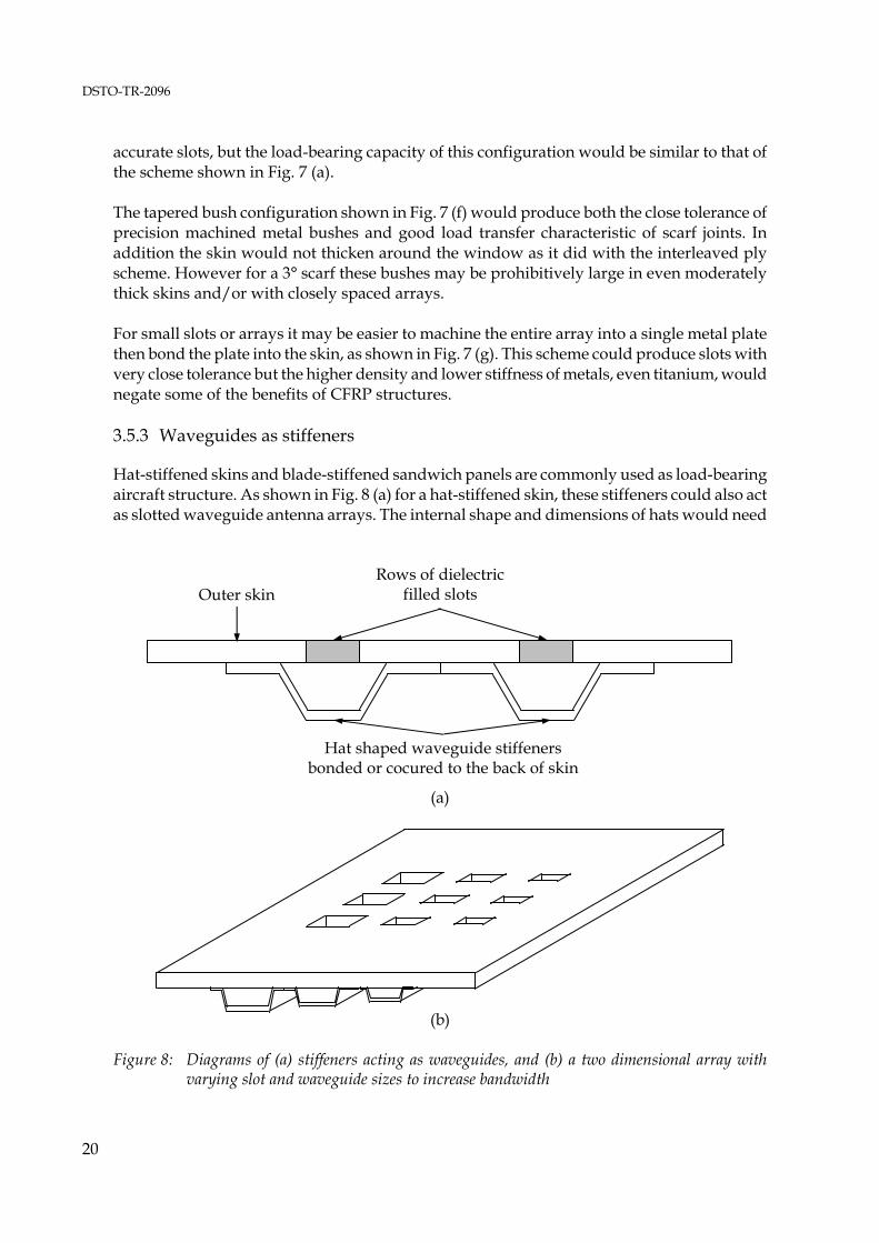
Hat-stiffened skins and blade-stiffened sandwich panels are commonly used as load-bearing aircraft structure. As shown in Fig. 8 (a) for a hat-stiffened skin, these stiffeners could also act as slotted waveguide antenna arrays. The internal shape and dimensions of hats would need
(a)
(b) Figure 8: Diagrams of (a) stiffeners acting as waveguides, and (b) a two dimensional array with
varying slot and waveguide sizes to increase bandwidth
Rows of dielectric filled slots Outer skin
Hat shaped waveguide stiffeners bonded or cocured to the back of skin

DSTO-TR-2096
21
to be designed so that they provided both the necessary structural support and also acted as waveguides for the desired frequencies. Fortunately the sizes of some standard rectangular waveguides are close to that of commonly used hat-stiffeners and sandwich panel thicknesses. For example WR-90 waveguides (with X-band operating frequencies of 8 - 12 GHz) are 22.86 x 10.16 mm, similar to the core depth of many sandwich panels. Additional design freedom may be obtained by filling waveguides with dielectric materials. If required, this may be used to extend the range of operating frequencies in waveguide while retaining their dimensions to satisfy structural requirements. Aircraft structures are relatively large. The outer skins of many would provide tens of square metres of surface area on which to install antennas for a wide range of frequencies without interference from each-other. However it may still be desirable to reduce the area of any particular array. One option to realise this would be to design individual slots with increased bandwidth. Another would be to use multiple waveguide stiffener dimensions as shown in Fig. 8 (b), each tuned for a different frequency band. A third would be to disperse the slots for a higher frequency among the slots for a lower frequency. For the final technique to be realised two issues must be resolved. The first arises because radiator separation tends to be of the same order as radiator size. There needs to be sufficient differences in the wavelength of each band for there to be sufficient space between the radiators in the low frequency band to accommodate the radiators for the higher frequency band. It is likely that this will be the case given the wide range of frequencies shown in Table 2. A 10:1 frequency separation will mean that, as shown in Fig. 9, almost all of the radiators for a 10 x 10 high frequency array would fit in the space between two adjacent radiators in the low frequency array. Secondly, and possibly more difficult will be feeding. It will not be possible to feed slots using straight hat-stiffener waveguides if the slots in the arrays are not aligned or are separated by slots that must be fed by different waveguides. Microstrip feed lines may be suitable for such situations. 3.6 Slotted Waveguide Antenna Stiffened Structure (SWASS)
SWASS is a refinement of the slot-array concept described in Section 3.5. Section 3.6 will describe some of the properties of waveguide antennas then how these may be integrated with stiffeners. 3.6.1 Slotted Waveguide Antenna (SWA)
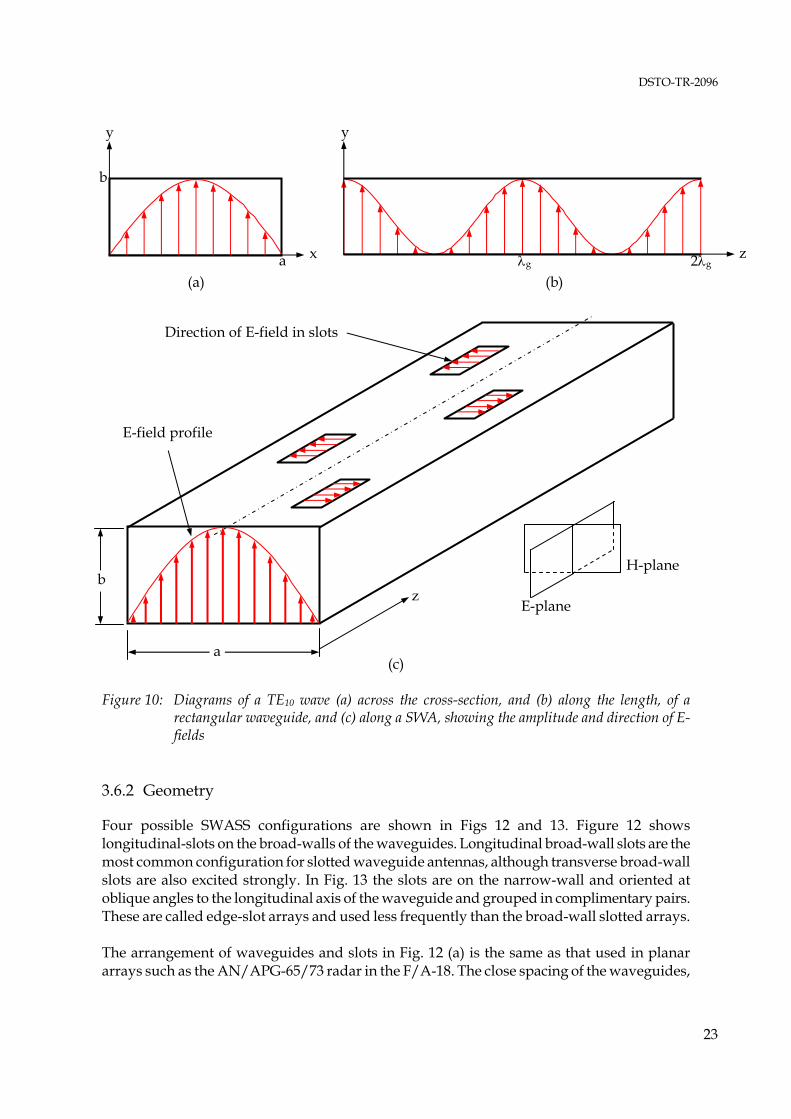
A rectangular waveguide is a length of electrically conducting tube with internal dimensions such that RF waves of particular frequencies propagate along that tube. The electric and magnetic fields of waves transmitted along waveguides have characteristic shapes that are known as propagating modes. In most applications only the fundamental TE10 propagation mode is desired because this transmits energy with minimum loss. A tube will not act as an efficient waveguide if its cross-section is either too small because the TE10 mode cannot propagate, or too large because the resultant additional propagation modes will increase losses. Figure 10 shows the cross-section of a TE10 wave in an SWA. The electrical field (E-field) of the

DSTO-TR-2096
22
(a) (b) Figure 9: Square arrays with node spacing’s of (a) d, and (b) 10d, and simulated slot radiators with
side lengths of 0.4d centred on each node RF wave points in the direction of the narrow-wall (dimension “b”) and, as shown in Fig. 10 (a), has a sinusoidal profile across the width of the waveguide with field strength of zero at the sidewalls and maximum along the centreline. As shown in Fig. 10 (b), the profile of the E-field along the waveguide is also sinusoidal with peaks and zeros at intervals of half a guided wavelength. Waves will be standing when the waveguide ends are electrically shorted or travelling when the ends of the waveguide are open. SWA are commonly known as leaky waveguide antenna. However, the mechanism by which these antennas operate is different to that suggested by their name. Energy does not move down waveguides like water flowing through a pipe and slots do not act merely like holes in the pipe. In reality, the variations in E-field strength across the width and along the length of waveguide walls sets up time varying electric (and associated magnetic) currents on these walls. Slots cut into the walls, such as those on the broad-wall shown in Fig. 10 (c), disrupt the currents in the walls and create electric fields across the slots. These fields will couple with the energy inside the waveguide and radiate that energy outside the waveguide. A typical SWA and its radiation pattern in the E- and H-planes are shown in Fig. 11. In this figure the antenna was oriented perpendicular to the ground so the azimuth pattern in Fig. 11 (b) was that of the H-plane from Fig. 10 (c) and the elevation plane shown in Fig. 11 (c) was that of the E-plane from Fig. 10 (c). Judicious positioning and sizing of the slots maximizes the efficiency of energy transfer from the waveguide to free space and controls the direction and polarization of the radiated energy. For example circular polarization may be obtained by using cross-shaped slots [10].
DSTO-TR-2096
23
(a) (b)
(c)
Figure 10: Diagrams of a TE10 wave (a) across the cross-section, and (b) along the length, of a rectangular waveguide, and (c) along a SWA, showing the amplitude and direction of E-fields
3.6.2 Geometry
Four possible SWASS configurations are shown in Figs 12 and 13. Figure 12 shows longitudinal-slots on the broad-walls of the waveguides. Longitudinal broad-wall slots are the most common configuration for slotted waveguide antennas, although transverse broad-wall slots are also excited strongly. In Fig. 13 the slots are on the narrow-wall and oriented at oblique angles to the longitudinal axis of the waveguide and grouped in complimentary pairs. These are called edge-slot arrays and used less frequently than the broad-wall slotted arrays. The arrangement of waveguides and slots in Fig. 12 (a) is the same as that used in planar arrays such as the AN/APG-65/73 radar in the F/A-18. The close spacing of the waveguides,
H-plane
E-plane
a
b
Direction of E-field in slots
E-field profile
z
b
y
x a z
y
λg 2λg

DSTO-TR-2096
24
(b) (a) (c) Figure 11: (a) A simple slotted waveguide antenna and the typical (b) azimuthal (H-plane) [11], and
(c) elevation (E-plane) [11] radiation patterns for such an antenna with the narrow-walls contacting each-other, allows the lateral distance between the slots (perpendicular to waveguide longitudinal axis) to be less than λ/2. This is important because a larger spacing, such as that shown in Fig. 12 (b), would produce unwanted sidelobes called grating lobes. It may be possible that the effect of grating lobes could be compensated by using very large numbers of radiating slots, however substantial modelling and testing would be required to validate this hypothesis. CLAS offers the possibility of very large numbers (tens of thousands) of radiating slots because the area available on the external surface of aircraft is generally much larger than that available for traditional waveguide arrays.

DSTO-TR-2096
25
(a)
(b) Figure 12: Diagrams showing SWASS configurations with longitudinal-slots on waveguide
stiffener broad-walls. (a) Blade-stiffened sandwich panel and (b) hat-stiffened skin
+x
+y
+z +z
+y
+x
+x
+y
+z +z
+y
+x

DSTO-TR-2096
26
(a)
(b) Figure 13: Diagram showing SWASS configurations with edge-slots on waveguide stiffener
narrow-walls. (a) Blade-stiffened sandwich panel and (b) hat-stiffened skin The layout shown in Fig. 12 (a) is classified as a blade-stiffened sandwich panel. In this configuration the waveguide broad-walls would be analogous to the face-sheets, supporting axial, bending and in-plane shear loads, while the narrow-walls would transfer loads between the face-sheets and prevent these outer skins from buckling. The strength and stiffness of this structure would be far greater for a given skin and blade thickness than the hat-stiffened arrangement shown in Fig. 12 (b). However this does not mean that only the blade-stiffened sandwich configuration would be used. There are many locations within aircraft structures where loads are oriented very strongly in one direction and structural stiffening in only that direction is required. It is also quite likely that hat-stiffened skins would be easier and cheaper to manufacture and support than blade-stiffened sandwich panels. However it is also possible that the spacing between the rows of waveguide stiffeners in the hat-stiffened configuration may be so large that unacceptable grating lobes would be generated.
+x
+y
+z +z
+y
+x
+x
+y
+z +z
+y
+x

DSTO-TR-2096
27
Longitudinal broad-wall slots tend to be quite narrow and would have little effect on load-bearing capacity, relative to that of the un-slotted structure, in the direction of the waveguide. This is fortunate because in well designed structure the hat- and blade-stiffeners are oriented in the direction of the major load. However broad-wall slots almost overlap in the longitudinal direction, producing an effective discontinuity along the entire length of the slot array. Load-bearing capacity is expected to be substantially lower perpendicular to this discontinuity. This may be important, and preclude even the blade-stiffened broad-wall slot designs, if significant in-plane shear or transverse axial loads exist. An alternative SWASS geometry for situations where loads were significant in more than one in-plane direction would be the edge-slot arrays shown in Fig. 13. The fractional area of skin cut by edge-slots would be much lower in the transverse direction (compared to longitudinal broad-wall slots) but larger in the stiffener direction. This increased fractional area cut by edge-slots in the stiffener direction may be partially compensated for by the deeper stiffeners. These would certainly increase bending stiffness substantially (doubling thickness increases bending stiffness by a factor of eight). Finally, the edge-slot design may permit a hat-stiffened skin (Fig. 13 (b)) to maintain the desired < λ/2 separation between the rows of slots because the waveguide stiffeners would be narrower in that direction. As with the broad-wall slot arrangement an inner face-sheet, as shown in Fig. 13 (a) may be added where greater stiffness/strength is required. Structural modelling would be required to establish the relative structural merits of SWASS with broad-wall and narrow-wall slots, and thus the potential applications for each. 3.6.3 Frequency range
3.6.3.1 Waveguides The potential operating frequency range of a SWASS antenna will be controlled by the cross-sectional shape and dimensions of the waveguide stiffeners. Although waveguides with elliptical and circular cross-sections are commercially available, only standard rectangular section waveguides have been considered because performance data is widely available and these waveguide cross-sections approximate that of hat-stiffeners. It is suspected that common stiffener cross-sectional shapes such as trapezoids and half-ellipses could be designed to propagate RF waves efficiently however the modelling and experimental validation that is required to verify this was beyond the scope of the work reported here. RF waves propagate within waveguides in discrete modes, with the mode name referring the shape of the electric and magnetic fields within the waveguide. For most applications, including SWASS, it is desired that the waveguide propagate only the dominant TE10 mode because this mode maximises energy transmission. The minimum frequency that can propagate in a waveguide is called the cut-off frequency (fco) and, for standard rectangular waveguides, is calculated using Equation 5. Although rectangular waveguides do operate in the single TE10 mode at frequencies from fco - 2fco, the practical limits are from 1.25fco - 1.89fco. For example, as shown in Table 3, the recommended

DSTO-TR-2096
28
frequency range for WR-90 waveguides, fco = 6.56 GHz, is 8.20 - 12.40 GHz, even though the waveguide will support single TE10 mode propagation from 6.56 - 13.11 GHz.
a2cfco = (5)
Where: c = speed of light (m s-1) a = width of broad-wall (m) Standard rectangular waveguides are available for frequencies ranging from L to G band, as shown in Table 3. It is estimated that the typical range of stiffener heights in aircraft structures is approximately 100 - 12 mm. Assuming that this range could be used for SWASS stiffeners then this would correspond to standard rectangular waveguides from R to K band. Thus, a first estimate for the potential frequency range of SWASS antennas is 1.70 – 26.5 GHz. The bandwidth for any particular SWASS antenna will probably be much smaller. As stated previously, the practical frequency range for any single waveguide is 1.25fco – 1.89fco. This equates to bandwidths of approximately 1.5:1 or 40 %. However, as described in Section 3.6.3.2, slots are narrowband and normally would not operate over the entire bandwidth of a waveguide. The bandwidth of a SWASS antenna array could be increased by varying the dimensions of slots or the slot separation within any single waveguide stiffener and/or using multiple waveguides, each with a different cross-section, in the part. 3.6.3.2 Slots in waveguides Literature on the topic of slot waveguide antennas, whether narrow- or broad-wall slots, has focused almost entirely on resonant slots. In analysing these arrays, the antenna is treated as a transmission line and the appropriate circuit equations invoked. Admittance (Y) is defined as Y = G + jB, where G is conductance and B is susceptance. For a slot antenna, at resonance the slot dimensions (length, width, angle) are such that B = 0 so that its admittance is real and equal to the conductance. The frequency range over which B can be considered zero is very narrow. Consequently bandwidths of 1 - 3 % (a few hundred MHz at a centre frequency of 10 GHz) are typical for resonant slots in waveguides. When designing resonant edge-slot antenna it is necessary to know the relation between slot Table 3: Frequency range and dimensions of selected standard rectangular waveguides
Inside dimensions (mm) Band Waveguide designation
Recommended frequency range (GHz) a b
L WR-650 1.12-1.70 165.10 82.55 R WR-430 1.70-2.60 109.22 54.61 X WR-90 8.2-12.4 22.86 10.16 K WR-42 18.0 – 26.5 10.70 4.32 G WR-5 140 – 220 1.30 0.65

DSTO-TR-2096
29
length and susceptance for the particular combination of slot angle, slot width, waveguide dimensions and frequency. It is difficult to obtain this data experimentally and the results for only a few combinations have been published. The author has obtained the design data from one group [12] and this approach may be used if it was decided to use a resonant edge slot antenna array in a SWASS. Resonant slots are in the order of 0.5λ0 (where λ0 is free space wavelength) long. However the short narrow-walls of waveguides are only around 0.4λ0 long. Thus narrow-wall slots are usually extended by cutting through the narrow-wall and down into the broad-walls. The parameter called “slot depth” is half the difference between the required slot length and the length available for the slot on the narrow-wall. While it is acceptable to penetrate into the broad-wall in stand-alone waveguides, this will not be acceptable in SWASS waveguide stiffeners. Firstly, extending a slot into the broad-wall could require the removal of some of the outer skin to allow access for a cutting tool into this wall. This would reduce further the structural strength of the SWASS. Secondly, slot extension into the broad-wall would direct some radiation against the back-face of the outer skin. This radiation would need to be absorbed, increasing weight and complexity of the SWASS. For these reasons it is strongly desired that the slots in SWASS be restricted to the outer skin (narrow-wall) only. Two publications have been found that focus on doing just this and both show promise for application to SWASS. In the first, it was predicted that changing the εr of the material within a slot would change the susceptance of the slot [13]. It was predicted that an open (εr = 1) 10 mm long, 1.6 mm wide, 25° edge slot in a WR-90 waveguide would be too short to resonate. However, if εr = 1.5 then the slot would resonate at 13 GHz while if εr = 3.5 it would resonate at 10.5 GHz. The predicted susceptance and conductance of slots was found to compare favourably to a numerical analysis but no experimental validation was reported. It should be possible to develop techniques that reliably fill SWASS slots with material of different εr (see Section 3.5.2.4). One possibility would be to machine slots in pre-cured SWASS then cover the slots with an appliqué that was produced from a material with the desired εr. The second publication described a 33.5 - 35.1 GHz frequency scanning, travelling wave, radar produced by Daimler-Benz Aerospace in 1995 [14]. A meander waveguide was made by folding a 5 m long Ka band (26.5 - 40.0 GHz) waveguide in a rectangular raster pattern. A travelling wave was launched at one end of the waveguide and an absorber used at the end of the waveguide to prevent reflections from the energy that remained after the slots. Effective energy transfer to the slots meant that the power loss to this absorber was only 1 dB. The close proximity of adjacent legs in the meandering waveguide meant that the edge slots could not extend down from the narrow-wall into the broad-wall. Thus below-resonant-length slots were investigated. When measuring the transmission S-parameters (S21) for 9 - 11 mm long crossed slot pairs in a WR-90 waveguide at 10.9 GHz, it was observed that the magnitude of S21 approached one and phase approached zero as slot length decreased. This behaviour was similar to that of a series-resonator circuit. From these measurements the radiation coupling loss per slot pair was calculated.

DSTO-TR-2096
30
The slot lengths and angles were designed to yield an amplitude profile that would produce the desired beam characteristics. The selected profile was a 20 element, -40 dB side lobe level, n = 4, Villeneuve distribution that had been factored to account for the experimentally measured coupling losses. The array was manufactured and performance measured experimentally. Although non-symmetrical shoulders were observed on the main beam because of the finite susceptance and associated phase error between the slots, and the first side lobe levels were -35 dB rather than -40 dB, the radar it appeared to function reasonably well. The bandwidth of this radar was over 6 % (2.1 GHz at 34.4 GHz), substantially greater than the 1 - 3 % for resonant slots. Unfortunately this is still around one order of magnitude less than the 40 % bandwidth available within any particular waveguide and desired for SWASS. Further research is required to develop slots that are capable of radiating across the entire bandwidth available in a waveguide. Alternative shapes, such as slot spirals, may be useful. Until the research to identify broadband slots is conducted then SWASS antennas would probably be restricted to bandwidths of 1 - 6 %. 3.6.4 Guided wavelength
It should be noted that the wavelength of a wave propagating in a waveguide (known as the guided wavelength λg) is not the same as that of the same frequency wave propagating in free space. Free space wavelength is given by the classical Equation 6 while guided wavelength in a rectangular waveguide is given by Equation 7.
fc
0 =λ (6)
2
c
2
0
g11
1
⎟⎟⎠
⎞⎜⎜⎝
⎛λ
−⎟⎟⎠
⎞⎜⎜⎝
⎛λ
=λ (7)
Where: f = frequency λg = guided wavelength λc = 2a where a is the width of the inside of the broad-wall 3.6.5 Radiation pattern
The radiation pattern produced by a single slot in a conducting ground plane is similar to that of a wire dipole - a doughnut shaped beam, omni-directional transverse to the radiator and zero along the longitudinal axis of the radiator. Figure 14 (a) shows one half of the radiation pattern for a half wavelength wire dipole oriented along the x-axis. This is very similar to the pattern from a slot in an infinite x-y ground plane. A slot array is a row of appropriately sized and located slots in a waveguide. Such an array

DSTO-TR-2096
31
(a) (b)
(c) Figure 14: The radiation pattern for a (a) single half wavelength dipole along the x-axis, sectioned
along the x-y plane, and a slot in the x-y plane, (b) row of slots oriented along the x-axis [15], and (c) planar array in the x-y plane [15]
modifies the pattern shown in Fig. 14 (a) by reducing the width of the beam in the H-plane (x-z plane), producing the pancake shaped pattern shown in Fig. 14 (b). In general, the greater the number of slots then the narrower the beam (smaller half power beam width (HPBW)) and the greater it’s gain. The typical design process for a slot array in a waveguide focuses on calculating the number, location, dimension and orientation of slots that are required to
x y
z
Planar slot array
Main beam
Sidelobes
z
x
y
θ
φ
Sidelobes
Edge slot array in
waveguide
Wire dipole
Slot in infinite x-y ground
plane
z
y
x

DSTO-TR-2096
32
produce the desired gain and HPBW in the main lobe while limiting the size and extent of sidelobes to an acceptable level. A planar array is created by extending the linear array from Fig. 14 (b) in the transverse direction. This focuses the pattern in both the H-plane (x-z plane) and E- plane (y-z plane) to create a pencil beam. In the case of Fig. 14 (c), the array is distributed over the x-y plane and the pencil beam oriented in the z-direction. 3.6.6 Beam steering
Beam steering is achieved by a coordinated variation of the phase between the waves incident at each slot in the array. If a planar array was fed through a single port that was manifolded into all of the waveguide stiffeners then the phase difference between each slot would be constant and dictated by the electrical length of waveguide between the feed and slot. Judicious selection of this length would produce a pencil beam oriented in the desired direction. Typically this would be broadside (z-axis in Fig. 14 (c)) or end-fire (x-axis in Fig. 14 (c)) but it could be another direction. The gain and HPBW of the beam would depend on the number of slots in the x- direction and waveguides in the y- direction. This beam would be called a staring beam and could only be steered by mechanically moving the entire array. If each waveguide were fed individually then the phase of the wave travelling down each waveguide may be varied independently and beam may be steered about the longitudinal axis of the waveguides (x-axis in Fig. 14 (c)) but not the transverse axis (y-axis in Fig. 14 (c)). Steering about the transverse axis (y-axis in Fig. 14 (c)) would require that the phase between adjacent slots within each of the waveguides be controlled. The conventional approach to steering the beam about this axis would be to either (i) retain the staring beam and mechanically steer the entire array about this axis, or (ii) use a separate T/R module for each slot. If the first approach were used then the antenna would no longer be CLAS, while the second could add considerable weight and complexity to the antenna. There are two potential approaches to produce full beam steering in SWASS. The first would be to produce SWASS components that contain multiple sub-arrays, each with a different (but fixed) beam angle about the transverse axis and steer about the longitudinal axis by controlling the phase between the sub-arrays. This may be practicable on large aircraft structures such as wing or fuselage skins because they have large surface areas. With tens of square metres (hundreds of square feet) available it may be practicable to produce many moderately sized sub-arrays, say 305 mm x 305 mm (1’ x 1’) arrays of 10 x 10 = 100 elements, each transmitting/receiving at a slightly different, but fixed, angle. The second approach hypothesises that an electronic device could be connected across each slot to control the phase radiated from that slot. A varactor is an electronic circuit element whose capacitance changes depending on the applied voltage [16]. It is possible that the capacitance could be controlled so that the slot radiates only when the RF wave reaches the desired strength, thereby creating an effective phase lag for that slot. Substantial modelling

DSTO-TR-2096
33
and experimental work would be required to verify test the feasibility of this approach in SWASS. 3.6.7 Waveguide termination
SWASS waveguides could be designed to operate with either standing or travelling waves. The former can be used to produce a resonant array while the latter would be used for travelling wave arrays. Standing waves are created by shorting or blanking the ends of the waveguide. Judicious selection of the waveguide length, position of the end shorts and spacing of the slots will create a standing wave with maximum power delivered to the slots. Travelling waves are created by leaving the waveguide ends open. If a travelling wave approach were chosen for SWASS an absorber would probably need to be located beyond the last slot to prevent radiation from being reflected back down the waveguide or leaking into the surrounding structure. 3.6.8 Feeding
A common way of feeding slotted waveguides is through a probe feed. With this feed the centre wire of a coaxial cable passes through a hole in the waveguide wall while the sheath is grounded to the waveguide wall. To create a standing wave an electrical short is located one quarter of a guided wavelength (λg/4) in the backward direction from the probe feed. Waves travelling in this backward direction reflect off the short and propagate in the forward direction. This reflected wave reinforces with the wave travelling in the forward direction directly from the probe feed. A wave propagating in one waveguide (the feed waveguide) may be used to feed other waveguides (radiating waveguide or other feed waveguides). The usual arrangement in planar slot arrays, such as those in many airborne radars, is to locate a feed waveguide behind, and transverse to, a bank of radiating waveguides. Slots cut in the common walls of the feed and fed waveguides allow the radiation to couple between these waveguides. The phase of any wave reaching a slot may be controlled by adjusting the location and size of the feed and radiating waveguides. This technique may be suitable for SWASS, although it will add thickness to the structure. 3.7 Enhanced structurally embedded microstrip
The researchers from the Pohang University of Science and Technology (Department of Mechanical Engineering, Pohang, Republic of Korea) have been major contributors to the CLAS literature. Their designs are based on integrating microstrip antenna into bonded honeycomb, two of which are shown in Fig. 15. In their designs, the inner skin supports structural loads, outer skins are a RF transparent window and internal layers support the skins, antenna radiator and antenna feed. The separation distance between these layers is determined with consideration to the RF requirements. Both single element antennas and antenna arrays have been manufactured and tested. The major limitation of these designs is that the skins have been manufactured from RF transparent GFRP or QFRP. Both of these materials have much lower stiffness than the

DSTO-TR-2096
34
(a) (b)
(c) Figure 15: CLAS concepts and test specimens from ref. [17]. Diagrams of (a) direct-fed stacked patch
antenna and (b) aperture-coupled patch antenna and (c) a photograph of a fabricated direct-fed stacked patch antenna
preferred CFRP. Neither GFRP nor QFRP are considered sufficiently stiff for the production of primary load-bearing aircraft structure. An alternative approach would be, as shown in Fig. 16, to replace these outer GFRP/QFRP face-sheets with CFRP face-sheets. Dielectric filled holes would couple the RF radiation from the microstrip, mounted inside the outer face-sheet, and free space. The permittivity of the dielectric plug could be controlled to miniaturise the microstrip and thus reduce the size of the hole in the outer face-sheet. Composite aircraft structure is designed to support DUL in the presence of manufacturing defects and operationally induced damage. Ideally it would be possible to incorporate the dielectric filled holes in a CFRP skin with no change in the design of the face-sheets or remainder of the structure. The size of an X-band microstrip antenna is in the order of 5 - 10

DSTO-TR-2096
35
Figure 16: Diagram of a concept for embedding microstrip antennas in sandwich panels mm diameter. It is possible that the hole in the face-sheet would be of the same size as the patch. Even if the holes needed to be larger, it should be relatively straightforward to accommodate this because designing composite aircraft structure to accommodate holes is a commonly performed process. The microstrip antenna would be positioned anywhere within the thickness of the sandwich panel to optimise RF performance while the sandwich panel thickness would be optimised for structural performance. With the configuration shown in Fig. 16 it may be possible for the outer CFRP face-sheet to act as the ground-plane. In addition antenna miniaturisation techniques, such as increasing the dielectric constant of the microstrip substrate or dielectric plug in front of the microstrip, may be used to reduce further the required hole size. Substantial modelling and testing would be required to validate these approaches.
4. SWASS for Aerosonde
4.1 Introduction
Uninhabited Air Vehicles (UAVs) that carry sensing, transmitting or jamming payloads can contribute to an Electronic Warfare (EW) capability. However the antennas for some EW systems are relatively heavy and/or bulky and so degrade the speed, range, endurance and payload of UAVs. It is hypothesized that some UAV performance may be restored by replacing such antennas with CLAS, thereby enhancing EW effectiveness.
Inner (load-bearing) CFRP face-sheet
Honeycomb core recessed for antenna package.
Depth set for structural performance
Outer (load-bearing) CFRP face-sheet
Dielectric plug between the microstrip and free space. Thickness set for RF performance
Microstrip deposited on dielectric substrate
Feed options Corporate microstrip line feed Coaxial wire feed
CFRP or metal coated CFRP ground plane
DSTO-TR-2096
36
During discussions with Dr Kim Brown, a DSTO scientist on a DSF at the United States Air Force Research Laboratory, Sensors Directorate, RF Sensor Technology Division, EW Techniques Development and Analysis Branch (AFRL-SNRE), Kim identified an opportunity to test this hypothesis. As part of his DSF he coordinated a TTCP flight trial at Fort Bliss, Texas, planned for October 2007. At the trial, UAVs fitted with jammers shall be flown against real threat radars. DSTO has purchased six Aerosonde Small Uninhabited Aerial Vehicles (SUAVs) [18] and is using these in its EW research program [19]. These SUAVs shall be used in the trial. It was proposed that the jammer antennas on one be replaced by CLAS and the resulting speed, range, endurance, payload and jamming effectiveness be measured. The remainder of Section 4 is a proposal that described a candidate conformal antenna concept and the steps necessary to evaluate this concept. In February 2007 it was decided not to pursue this proposal because the pressure to produce a working demonstrator for a specific application in a tight timeframe would divert resources from a generic validation of the SWASS concept and a greater understanding of the potential design space for this concept. 4.2 Background
The weight and cost of many EW systems, such as sensors, receivers and jammers are sufficiently low (a few kilograms and a few thousand dollars) that they may be carried as payloads in SUAVs. The advantages of SUAVs are that they can traverse battlefields within time periods suitable for tactical roles, be networked and replaced at relatively low cost. SUAVs fitted with appropriate systems could contribute significantly to jamming and suppression of enemy air defences, electronic support measures and signals intelligence [19]. Although many EW systems can be carried by SUAVs, their weight and size do reduce performance (speed, range, endurance and payload). Intuitively, restoring performance of a SUAV to that of the “clean” platform would maximize its effectiveness as an EW platform. It is hypothesized that one way to do this is to replace heavy and/or bulky antennas with CLAS. 4.3 Aerosonde
4.3.1 Basic airframe
Some characteristics and performance data for the Aerosonde SUAV are shown in Table 4. A photograph and diagrams of a “clean” Aerosonde is shown in Figs 17 and 18 respectively. 4.3.2 Systems requiring antenna
A range of systems on DSTO’s Aerosondes require antennas. These include basic control and navigation of the SUAV and specialist EW systems. Table 5 lists some of these systems and the required antenna characteristics. Figure 19 shows an Aerosonde fitted with the antennas for a DSTO jammer.

DSTO-TR-2096
37
Table 4: Published specifications of the Aerosonde [20] Parameter Value
Speed 65-115 km h-1 Range >3000 km Endurance >30 h Payload 2.5 kg Max. Altitude <20,000 ft Weight 12-14 kg Wingspan 2.9 m
Figure 17: Photograph of a “clean” Aerosonde SUAV [21] 4.4 Antenna selection
It was decided to focus this proposal on the T/R antennas for the DSTO jammer. This was done because these antennas were perceived as being relatively large and heavy and so would offer the greatest potential for performance gains through drag and weight reductions. In addition, of all the systems detailed in Table 5, the jammer T/R antennas operate at the highest frequency so the antenna components would be the smallest, making them more amenable to replacement by SWASS.

DSTO-TR-2096
38
Figure 18: Drawings of the Aerosonde SUAV [22]
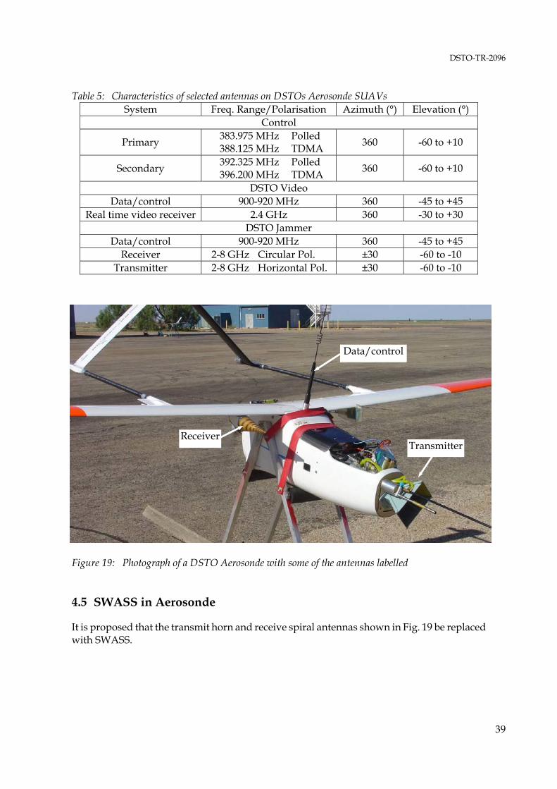
DSTO-TR-2096
39
Table 5: Characteristics of selected antennas on DSTOs Aerosonde SUAVs System Freq. Range/Polarisation Azimuth (°) Elevation (°)
Control
Primary 383.975 MHz Polled 388.125 MHz TDMA 360 -60 to +10
Secondary 392.325 MHz Polled 396.200 MHz TDMA 360 -60 to +10
DSTO Video Data/control 900-920 MHz 360 -45 to +45
Real time video receiver 2.4 GHz 360 -30 to +30 DSTO Jammer
Data/control 900-920 MHz 360 -45 to +45 Receiver 2-8 GHz Circular Pol. ±30 -60 to -10
Transmitter 2-8 GHz Horizontal Pol. ±30 -60 to -10
Figure 19: Photograph of a DSTO Aerosonde with some of the antennas labelled 4.5 SWASS in Aerosonde
It is proposed that the transmit horn and receive spiral antennas shown in Fig. 19 be replaced with SWASS.
Receiver Transmitter
Data/control

DSTO-TR-2096
40
4.5.1 Size
An estimate was made of the typical cross-section of an Aerosonde wing. This was drawn approximately full-size in Fig. 20, together with a number of standard rectangular waveguides. The drawing suggests that a C-band rigid rectangular waveguide, with a minimum usable frequency of 5.85 GHz, would be the largest standard rectangular waveguide that would fit inside an Aerosonde wing. As indicated in Table 5, this waveguide Figure 20: Full-scale drawings of the cross-section of selected rigid rectangular waveguides and an
estimate of the typical cross-section of an Aerosonde wing
X-Band 8-12GHz
1.00” x 0.50”
C-Band 5.85-8.20 GHz 1.50” x 0.75”
R-Band 1.70-2.60 GHz 4.46” x 2.31”
H-Band
3.95-5.85 GHz 2.00” x 1.00”
S-Band 2.60-3.95 GHz 3.00” x 1.50”

DSTO-TR-2096
41
would support somewhat less than half of the desired frequency range for the jammer. It is possible that non-standard shapes may exist that support lower frequencies with the same outer dimensions, however identifying them was beyond the scope of this proposal. Waveguides with intermediate cross-sections and therefore intermediate frequency bands would also fit the wing. Such tubes could readily be produced either as an off-the-shelf tube or by machining down suitable bar or tube stock. 4.5.2 Number of antennas
The T/R antennas in the DSTO jammer system operate simultaneously. Thus separate transmit and receive antennas would be required. One way of achieving this would be to mount the transmit antenna in one wing and the receive antenna in the opposite wing. 4.5.3 Location
A major factor in determining the radiation pattern relative to the aircraft will be the orientation of the SWASS on the aircraft. The examples described in this proposal focus on installing the SWASS inside the wing with the waveguide longitudinal oriented span-wise. However, as shown in Fig. 21, there are a range of installation locations that would allow substantially different radiation patterns. Figure 21: Possible SWASS installation locations and orientations on an Aerosonde
Span-wise in wing
Chord-wise in wing
Vertical in fuselage
Longitudinal in fuselage Wrapped around fuselage
Tail boom
Leading edge

DSTO-TR-2096
42
Obviously there will be advantages and limitations for each location. For example SWASS mounted chord-wise in the wing or vertical in the fuselage would be much shorter than that mounted span-wise in the wing. Similarly the depth (“b” dimension) of SWASS installed in the fuselage may be limited to the thickness of the honeycomb core, around 10 mm. 4.5.4 Installation
The simplest installation approach would be, as shown in Fig. 22 (a), to insert a stand-alone
(a)
(b)
(c)
(d) Figure 22: Drawings showing potential conformal antenna approaches
Wing cross-section
Rigid rectangular waveguide SWA or cavity-backed slot-spiral antenna bonded to inside wall of
wing-skin
Shaped SWA (machined metal or dielectric foam core wrapped with metal foil) installed behind
wing-skin
Remove section of wing-skin and replace with SWA
(machined metal or dielectric foam core wrapped with CFRP)
New CFRP wing-skin with integral blade stiffener(s) located so that they form
waveguide walls. May use dielectric foam core

DSTO-TR-2096
43
SWA into the wing and bond it to the inner wing-skin. Aerosonde wing-skins are constructed from GFRP and so would be reasonably transparent to RF radiation. Installing the SWA inside the wings should not markedly reduce antenna performance and it will not be load-bearing. This approach would be suitable for a range of other stand-alone antenna types, such as the cavity-backed slot-spiral antenna described in Section 3.2. Such alternative antenna types may be considered if the pattern or bandwidth of SWASS proved to be unsuitable. The cross-section of the SWASS waveguide could be shaped to fit convenient features such as the leading edge. This option is shown in Fig. 22 (b). It is unlikely that the internal profile of wings, or other features in SUAVs, would remain sufficiently constant for standard rectangular or circular waveguides to remain flush along their length. Therefore this option would probably require custom made waveguides such as the leading edge profile shown. A more structurally efficient approach would be to cut out and remove some of the wing-skin and replace it with SWASS, as shown in Fig. 22 (c). The SWASS would be adhesively bonded into the cut-out such that its outer skin finished flush with the pre-existing surface of the wing-skin. The stiffening effect of the SWASS would mean that the wing-skin could be thinner and still support flight-loads. However implementing this by thinning down an already thin wing-skin would be quite difficult. The most structurally efficient approach would be to re-manufacture the entire wing with internal blades that act both as stiffeners and waveguide walls, as shown in Fig. 22 (d). These stiffeners would allow the wing-skin thickness to be reduced while retaining sufficient strength and stiffness. If the GFRP material were retained as the construction material then the waveguide walls would need to be lined with a conductor such as aluminium or copper foil. An attractive alternative would be to manufacture the wing from CFRP. This material is structurally superior, stiffer and stronger, to GFRP and its conductivity may sufficiently high that a liner on the waveguide walls would not be required. The approaches represented in Fig. 22 (c) and (d) could also be used to install SWASS into the Aerosonde’s honeycomb stiffened fuselage. The outer skin and honeycomb core could be cut away then the SWASS bonded onto the exposed inner skin. A more efficient approach would be to re-manufacture the fuselage with integral blade stiffeners, positioning the structural stiffeners such that they also act as waveguide walls. 4.6 Research program
The concepts detailed in Section 4.5 may be tested by conducting the following research program:
1. Develop detailed specifications for the required T/R antenna performance. 2. Perform a first-order evaluation of potential SWASS concepts and select the concept
that shows the most promise. Terminate project if no realistic candidate can be identified.
3. Perform detailed structural analysis and RF modelling of the selected candidate. 4. Experimentally validate the RF models and predictions. Use simplified or generic
specimens where possible.
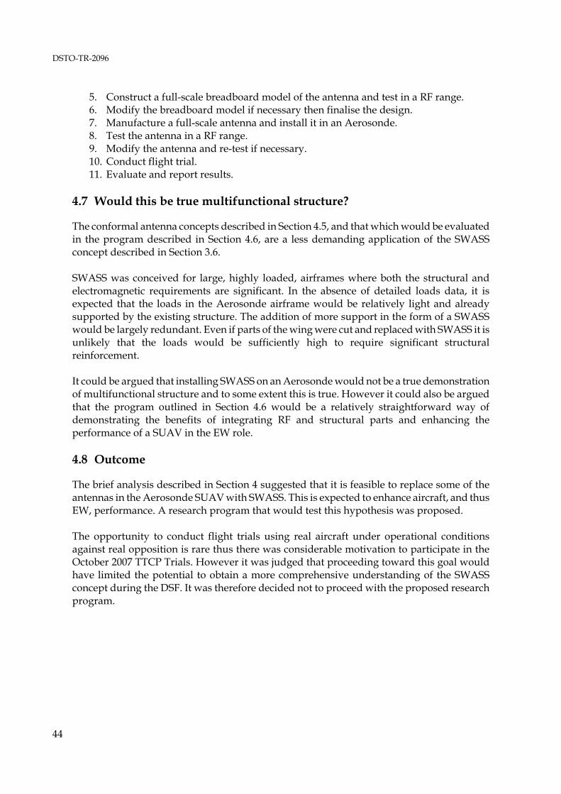
DSTO-TR-2096
44
5. Construct a full-scale breadboard model of the antenna and test in a RF range. 6. Modify the breadboard model if necessary then finalise the design. 7. Manufacture a full-scale antenna and install it in an Aerosonde. 8. Test the antenna in a RF range. 9. Modify the antenna and re-test if necessary. 10. Conduct flight trial. 11. Evaluate and report results.
4.7 Would this be true multifunctional structure?
The conformal antenna concepts described in Section 4.5, and that which would be evaluated in the program described in Section 4.6, are a less demanding application of the SWASS concept described in Section 3.6. SWASS was conceived for large, highly loaded, airframes where both the structural and electromagnetic requirements are significant. In the absence of detailed loads data, it is expected that the loads in the Aerosonde airframe would be relatively light and already supported by the existing structure. The addition of more support in the form of a SWASS would be largely redundant. Even if parts of the wing were cut and replaced with SWASS it is unlikely that the loads would be sufficiently high to require significant structural reinforcement. It could be argued that installing SWASS on an Aerosonde would not be a true demonstration of multifunctional structure and to some extent this is true. However it could also be argued that the program outlined in Section 4.6 would be a relatively straightforward way of demonstrating the benefits of integrating RF and structural parts and enhancing the performance of a SUAV in the EW role. 4.8 Outcome
The brief analysis described in Section 4 suggested that it is feasible to replace some of the antennas in the Aerosonde SUAV with SWASS. This is expected to enhance aircraft, and thus EW, performance. A research program that would test this hypothesis was proposed. The opportunity to conduct flight trials using real aircraft under operational conditions against real opposition is rare thus there was considerable motivation to participate in the October 2007 TTCP Trials. However it was judged that proceeding toward this goal would have limited the potential to obtain a more comprehensive understanding of the SWASS concept during the DSF. It was therefore decided not to proceed with the proposed research program.

DSTO-TR-2096
45
5. Electromagnetic Modelling
5.1 Model
Models of a simplified SWASS antenna, consisting of four edge slots in a three guided wavelength long section of WR-90 waveguide, were created using the EM modelling software FEKO. The basic shape of these models is shown in Fig. 23 and the parameters named in this figure are described in Table 6. Each model was meshed with 1750-1850 elements, typical examples of which are shown in Fig. 24. The waveguide models were excited with 10 GHz standing TE10 waves and the method of moments (MoM) solution invoked to predict the surface currents on the waveguide walls, E- fields within the waveguide and radiation pattern. Solution times were in the order of 30 seconds. 5.2 FEKO modelling
5.2.1 Effect of feed
The first parameter to be investigated was the method used to create the RF wave. Feeding can be implemented in FEKO either through a wire probe or by an impressed excitation. A common way of launching a RF wave inside a waveguide is to connect a coaxial cable to the waveguide. The coaxial sheath is grounded to the waveguide wall while the wire core passes through a hole in the waveguide wall and into the waveguide. The location of the feed wire is selected to produce the desired wave. Simulating this in FEKO was achieved by creating a “wire probe” at the same location as the coaxial core wire would be in an actual waveguide, electrically connecting the probe to the walls of the waveguide (the “union” action in FEKO) and defining the wire probe to be a feed port. The feed probe in the FEKO model of the SWASS waveguide was located a distance of λg/4 from the end of the waveguide so that waves reflected from this end would reinforce with those radiating directly from the wire. An electrical short was placed λg/4 beyond the last slot, thereby producing a standing wave. FEKO also has the capability to launch TEmn or TMmn waves from a surface using the AW Excitation within the EDITFEKO advanced solution settings and scripting tool. The TE10 wave in the SWASS model was launched from the end of the waveguide, the position of which was changed so that it coincided with the location of the wire port, a distance of λg from the first slot. The procedure for obtaining the impressed wave was to: define the vertices of the launch surface, ensure that the surface normal pointed in the desired direction of wave propagation, mesh the surface, save the model. This created model.cfx, model.cfm and model.pre files, open the model.pre file and choose Excitations AW define the names of the launch face, face vertices and excitation mode (TE10 in this case),
and

DSTO
-TR-2096
46
Figure 23: Diagram showing a FEKO model of a SWASS waveguide and the X, Y, Z coordinates of the key features
Slot4 Corner 1 Corner 2 X = -3*SlotSep/2-SlotLprojxaxis/2-SlotWprojxaxis/2 -3*SlotSep/2-SlotLprojxaxis/2+SlotWprojxaxis/2 Y = SlotLprojyaxis/2-SlotWproyyaxis/2 SlotLprojyaxis/2+SlotWproyyaxis/2 Z = -DimWTN/2 -DimWTN/2 Corner 3 Corner 4 X = -3*SlotSep/2+SlotLprojxaxis/2+SlotWprojxaxis/2 -3*SlotSep/2+SlotLprojxaxis/2-SlotWprojxaxis/2 Y = -SlotLprojyaxis/2+SlotWproyyaxis/2 -SlotLprojyaxis/2-SlotWproyyaxis/2 Z = -DimWTN/2 -DimWTN/2
Radius 1 (at rear of slot) Centre point X = -3*SlotSep/2-SlotLprojxaxis/2 Y = SlotLprojyaxis/2 Z = -DimWTN/2 Radius (X) = SlotWidth/2 (Y) = SlotWidth/2
Radius 2 (at front of slot) Centre point X = -3*SlotSep/2+SlotLprojxaxis/2 Y = -SlotLprojyaxis/2 Z = -DimWTN/2 Radius (X) = SlotWidth/2 (Y) = SlotWidth/2
+X
+Y +Z
End1 Corner 1 X = 3*SlotSep/2+DimPortGap+DimE1S+DimWTE/2 Y = -Dimb/2-DimWTB/2 Z = -DimWTN/2 Corner 2 X = 3*SlotSep/2+DimPortGap+DimE1S+DimWTE/2 Y = Dimb/2+DimWTB/2 Z = -DimWTN/2 Corner 3 X = 3*SlotSep/2+DimPortGap+DimE1S+DimWTE/2 Y = Dimb/2+DimWTB/2 Z = -DimWTN-Dima-DimWTN/2 Corner 4 X = 3*SlotSep/2+DimPortGap+DimE1S+DimWTE/2 Y = -Dimb/2-DimWTB/2 Z = -DimWTN-Dima-DimWTN/2
Wire feed probe End 1 X = 3*SlotSep/2+DimPortGap Y = -Dimb/2-DimWTB/2 Z = -DimWTN-Dima/2 End 2 X = 3*SlotSep/2+DimPortGap Y = Dimb/2+DimWTB/2 Z = -DimWTN-Dima/2
Slot1 Corner 1 Corner 2 X = 3*SlotSep/2+SlotLprojxaxis/2-SlotWprojxaxis/2 3*SlotSep/2+SlotLprojxaxis/2+SlotWprojxaxis/2 Y = SlotLprojyaxis/2+SlotWproyyaxis/2 SlotLprojyaxis/2-SlotWproyyaxis/2 Z = -DimWTN/2 -DimWTN/2 Corner 3 Corner 4 X = 3*SlotSep/2-SlotLprojxaxis/2+SlotWprojxaxis/2 3*SlotSep/2-SlotLprojxaxis/2-SlotWprojxaxis/2 Y = -SlotLprojyaxis/2-SlotWproyyaxis/2 -SlotLprojyaxis/2+SlotWproyyaxis/2 Z = -DimWTN/2 -DimWTN/2
Radius 1 (at rear of slot) Centre point X = 3*SlotSep/2+SlotLprojxaxis/2 Y = SlotLprojyaxis/2 Z = -DimWTN/2 Radius (X) = SlotWidth/2 (Y) = SlotWidth/2
Radius 2 (at front of slot) Centre point X = 3*SlotSep/2-SlotLprojxaxis/2 Y = -SlotLprojyaxis/2 Z = -DimWTN/2 Radius (X) = SlotWidth/2 (Y) = SlotWidth/2
Slot2 Corner 1 Corner 2 X = SlotSep/2-SlotLprojxaxis/2-SlotWprojxaxis/2 SlotSep/2-SlotLprojxaxis/2+SlotWprojxaxis/2 Y = SlotLprojyaxis/2-SlotWproyyaxis/2 SlotLprojyaxis/2+SlotWproyyaxis/2 Z = -DimWTN/2 -DimWTN/2 Corner 3 Corner 4 X = SlotSep/2+SlotLprojxaxis/2+SlotWprojxaxis/2 SlotSep/2+SlotLprojxaxis/2-SlotWprojxaxis/2 Y = -SlotLprojyaxis/2+SlotWproyyaxis/2 -SlotLprojyaxis/2-SlotWproyyaxis/2 Z = -DimWTN/2 -DimWTN/2
Radius 1 (at rear of slot) Centre point X = SlotSep/2-SlotLprojxaxis/2 Y = SlotLprojyaxis/2 Z = -DimWTN/2 Radius (X) = SlotWidth/2 (Y) = SlotWidth/2
Radius 2 (at front of slot) Centre point X = SlotSep/2+SlotLprojxaxis/2 Y = -SlotLprojyaxis/2 Z = -DimWTN/2 Radius (X) = SlotWidth/2 (Y) = SlotWidth/2
Slot3 Corner 1 Corner 2 X = -SlotSep/2+SlotLprojxaxis/2-SlotWprojxaxis/2 -SlotSep/2+SlotLprojxaxis/2+SlotWprojxaxis/2 Y = SlotLprojyaxis/2+SlotWproyyaxis/2 SlotLprojyaxis/2-SlotWproyyaxis/2 Z = -DimWTN/2 -DimWTN/2 Corner 3 Corner 4 X = -SlotSep/2-SlotLprojxaxis/2+SlotWprojxaxis/2 -SlotSep/2-SlotLprojxaxis/2-SlotWprojxaxis/2 Y = -SlotLprojyaxis/2-SlotWproyyaxis/2 -SlotLprojyaxis/2+SlotWproyyaxis/2 Z = -DimWTN/2 -DimWTN/2
Radius 1 (at rear of slot) Centre point X = -SlotSep/2+SlotLprojxaxis/2 Y = SlotLprojyaxis/2 Z = -DimWTN/2 Radius (X) = SlotWidth/2 (Y) = SlotWidth/2
Radius 2 (at front of slot) Centre point X = -SlotSep/2-SlotLprojxaxis/2 Y = -SlotLprojyaxis/2 Z = -DimWTN/2 Radius (X) = SlotWidth/2 (Y) = SlotWidth/2
End2 Corner 1 X = -3*SlotSep/2-DimE2S-DimWTE/2 Y = -Dimb/2-DimWTB/2 Z = -DimWTN/2 Corner 2 X = -3*SlotSep/2-DimE2S-DimWTE/2 Y = Dimb/2+DimWTB/2 Z = -DimWTN/2 Corner 3 X = -3*SlotSep/2-DimE2S-DimWTE/2 Y = Dimb/2+DimWTB/2 Z = -DimWTN-Dima-DimWTN/2 Corner 4 X = -3*SlotSep/2-DimE2S-DimWTE/2 Y = -Dimb/2-DimWTB/2 Z = -DimWTN-Dima-DimWTN/2

DSTO
-TR-2096
47
Table 6: The name, description and values of variables used to construct the FEKO models shown in Fig. 23 Variable Full variable name Description Expression Value
Dima Dimension a Waveguide depth 22.86 mm 22.86 mm Dimb Dimension b Waveguide width 10.16 mm 10.16 mm
DimE1S Dimension from End 1 to Slot 1 Distance from feed end of waveguide to first slot (or wire feed) Lamg/4 9.9267798 mm
DimE2S Dimension from End 2 to Slot 1 Distance from far end of waveguide to last slot Lamg/4 9.9267798 mm
DimPortGap Dimension Port Gap Distance from wire feed port to first slot Lamg 39.707119 mm DimWTB Dimension Wall Thickness Broad Thickness of broad-walls 0.5 mm 0.5 mm DimWTE Dimension Wall Thickness End Thickness of end-walls 0.5 mm 0.5 mm DimWTN Dimension Wall Thickness Narrow Thickness of narrow-walls 0.5 mm 0.5 mm
Lam0 Lamda zero Free space wavelength 1000*c0/Freq 29.979246 mm Lamco Lamda CO Wavelength at cut-off frequency 2*Dima 45.72 mm
Lamg Lambda G Guided wavelength 1/sqrt((1/Lam0)^2-(1/Lamco)^2) 39.707119 mm
MeshE Mesh – Elements Element edge length Lamg/10 3.9707119 mm MeshR Mesh – Radius Wire segment radius Lamg/600 0.0661785 mm MeshS Mesh – segment Mesh segment length Lamg/40 0.9926780 mm
SlotAngleDeg Slot Angle in Degrees 20.0° 20.0° SlotAngleRad Slot Angle in Radians SlotAngleDeg*pi/180 0.3490659 rad.
SlotLength Slot Length Length of straight sides of slot. Radiused ends must be added to this SlotLength 6.2-8.9 mm
SlotLengthwithradiusends
Total Slot Length including both radiused ends SlotLengh+SlotWidth 7.8-10.5 mm
SlotLprojxaxis Slot Length as projected onto x axis SlotLength*sin(SlotAngleRad) 2.8729692 mm SlotLprojyaxis Slot Length as projected onto y axis SlotLength*cos(SlotAngleRad) 7.8934180 mm
SlotSep Separation between slots Lamg/2 19.853560 mm SlotWidth Slot width 1.6 mm 1.6 mm
SlotWprojxaxis Slot Width as projected onto x axis SlotWidth*cos(SlotAngleRad) 1.5035082 mm SlotWprojyaxis Slot Width as projected onto y axis SlotWidth*sin(SlotAngleRad) 0.5472322 mm

48
Figure 24: Screen-dumps of typical FEKO models run the FEKO MoM solver from the EDITFEKO screen. The SWASS waveguides models were constructed from the default material, a perfect electrical conductor (PEC) and had the same inner dimensions as a standard WR-90 waveguide, 22.86 mm x 10.16 mm. The four slots were; 2.00 mm wide, oriented at ±70° to the longitudinal axis of the waveguide and extended 2.8 mm into the broad-wall. The gap between the final slot or wire probe and the end-wall was λg/4. Simulations were run to test the difference between the AW Excitation and the wire probe method. Figure 25 shows the resultant X-Z plane (H-plane) radiation pattern from these two excitation methods. The amplitudes produced by each method was different because the (a) (b) Figure 25: (a) Polar and (b) linear H-plane antenna patterns for wire probe feed and impressed TE10
wave (AW Card function) on a four edge-slot array in a WR-90 waveguide
z x
y x y z

DSTO-TR-2096
49
default excitation voltages that were used in each were not calibrated to produce the same field strength within the waveguides. There appeared to be very little difference in the patterns predicted by the two excitation methods. All subsequent models used the wire probe method. 5.2.2 Effect of inter-waveguide skins
In SWASS the waveguides would form part of a larger structure, either a hat-stiffened skin or a blade-stiffened sandwich. The first step in evaluating the effect of this additional structure on the radiation pattern was to determine the effect of a front-face skin. Models were created that contained the slotted waveguide and a half wavelength wide skin running the length of the waveguide. This was done for two slot cases, 0.00 mm (slots in the edge-wall only) shown in Fig. 26 (a) and 2.80 mm deep (the same configuration as in Section 5.2.1) shown in Fig. 26 (b). The predicted radiation patterns are shown in Fig. 26. It was observed that the addition of the skin was predicted to have little effect on gain, H-plane HPBW and sidelobe location. However the side-lobe level (SLL) was predicted to increase over 5 dB for slots that extend into the broad-wall and 3 dB for slots restricted to the narrow-wall only. It is most likely that this increase was due to reflections from the skin. Extending the skin further was expected to increase the SLL even more, however this was not modelled. 5.2.3 Effect of skin material
The waveguide walls were modelled as (i) PEC, (ii) “thin dielectric” and (iii) “lossy conductor with metallic medium”. The default material was 0.1 mm thick PEC. PEC walls are also the idealised basis on which many EM analytical solutions are founded. Predictions made with PEC walls were therefore considered a baseline for SWASS. The conductivity of CFRP is finite and this was expected to affect significantly the radiation pattern relative to that from a waveguide manufactured from PEC. σcarbon fibres ≈ 104 S m-1, two orders of magnitude less than that of metals. As indicated previously, under DC conditions σCFRP UD 0° ≈ 103 S m-1, σCFRP UD 90° ≈ 10 S m-1 and σCFRP MD in-plane ≈ 103 S m-1. FEKO can account for finite conductivity in two ways, the “thin dielectric” and the “lossy conductor with metallic medium”. Predictions were made to test the effect of these two FEKO solution techniques. Models were created with each of these materials. The PEC was 0.1 mm thick, the thin dielectric and metallic medium were 1.27 mm (0.05”) thick with a conductivity of 1000 S m-1. This thickness was chosen because it is the thickness of standard metallic WR-90 waveguides. A double wall waveguide, constructed of 0.1 mm PEC walls separated by 1.27 mm, was also modelled to examine the effect of finite wall thickness. Figure 27 shows the predicted H-plane radiation patterns. The PEC and layered dielectric were practically identical. For the model with finite PEC walls the central beam was predicted
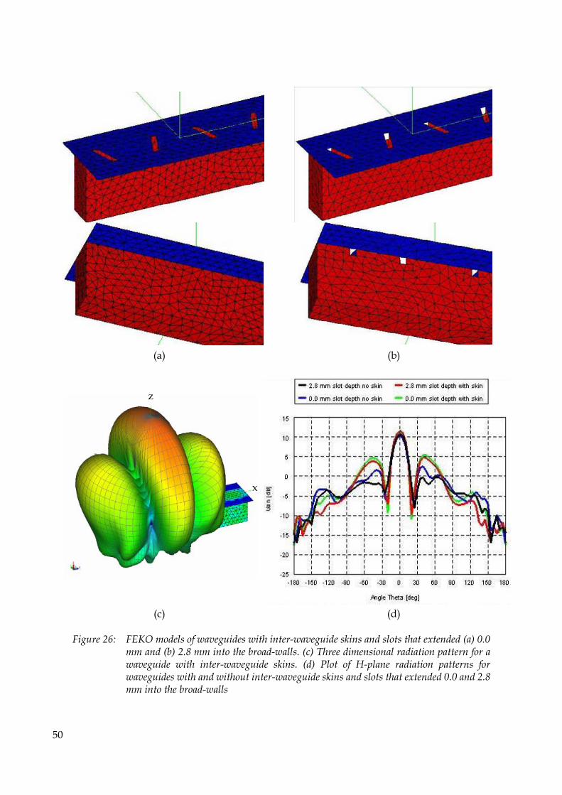
50
(a) (b) (c) (d) Figure 26: FEKO models of waveguides with inter-waveguide skins and slots that extended (a) 0.0
mm and (b) 2.8 mm into the broad-walls. (c) Three dimensional radiation pattern for a waveguide with inter-waveguide skins. (d) Plot of H-plane radiation patterns for waveguides with and without inter-waveguide skins and slots that extended 0.0 and 2.8 mm into the broad-walls
x
z

DSTO-TR-2096
51
Figure 27: Predicted H-plane radiation patterns for waveguide model with different materials to be very close to that of the single wall PEC, however the first null was deeper, the first SLL slightly higher and the side lobe shape smoother. In contrast the metallic medium model predicted an approximately 5 dB lower gain, 3 dB lower SLL and a different pattern shape. It was decided that all subsequent models would be constructed using the layered dielectric as this was expected to be the most reasonable representation of CRFP waveguides. 5.2.4 Effect of conductivity
As indicated previously, it was expected that the finite conductivity of CFRP composites would affect significantly the radiation pattern from a SWASS antenna. Four identical models, except for the conductivity of the layered dielectric waveguide skin, were analysed and the results are shown in Fig. 28. The predicted H-plane pattern of a waveguide constructed from 1.27 mm (0.05”) thick, σ = 1000 S m-1, dielectric was almost identical to the waveguide modelled as a 0.1 mm PEC. At σ = 100 S m-1 the gain fell by 7 dB and SLL by 1 dB relative to the PEC. The shape of the pattern was very similar although the sidelobes were smoother and more clearly defined. A fourth simulation, with σ = 10 S m-1, predicted a severely distorted pattern. There was no longer a single broadside peak with distinct sidelobes, but rather two very weak peaks oriented at ±45° from the longitudinal axis of the waveguide and no clear sidelobes. These results predict that the radiation pattern from CFRP waveguides should be reasonably close to that predicted for PEC waveguides provided that the effective conductivity of the

52
(a) (b) (c) (d) Figure 28: (a) Predicted H-plane radiation patterns for layered dielectric waveguides modelled with
different conductivities. Three dimensional representations of the antenna patterns for conductivities of (b) 1000 S m-1, (c) 100 S m-1 and (d) 10 S m-1
waveguide walls remained around 1000 S m-1. It is uncertain whether this can be achieved in real CFRP waveguides. Certainly the conductivity of a quasi-isotropic CFRP laminate under direct current (DC) conditions is close to 1000 S m-1. Although conductivity is nominally independent of frequency, there is still some uncertainty regarding the behaviour of laminates at RF.

DSTO-TR-2096
53
The finite thickness of non-conducting resin that covers the conductive carbon fibres in a CFRP composite was not expected to influence dramatically the RF propagation in the waveguide. Certainly this layer may create some resistive (Ohmic) loss, but energy was expected to simply penetrate through the resin for the few tens of micrometres of resin skin down to the fibres. Of less certainty was the effect of ply stacking sequence. This may be particularly important because of the two order of magnitude difference in the longitudinal and transverse DC conductivity, 1000 S m-1 and 10 S m-1 respectively, for unidirectional plies. This difference raised two questions. The first was whether waveguide losses could be reduced by orienting the inner ply either (i) parallel to the longitudinal axis of the waveguide so that the conductive path would be in the direction of propagation, or (ii) perpendicular to the edge wall so that the fibres would be parallel to the changing current in the edge walls? The second was, whether orientation would be unimportant because the in-plane conductivity of a multi-ply, multi-angle, laminate would be effectively quasi-isotropic due to the large number of contacting fibres between adjacent plies? The skin depth concept may assist in answering these questions. RF electrical currents do not flow through the entire cross-section of a conductor as visualised in the classical “water-through-a-garden-hose” explanation of DC current flow. Rather, RF currents flow preferentially near the surface, with peak current at the surface and a gradually reducing magnitude deeper into the conductor. The depth that the current falls to 37 % (= 1/e) of its surface value is known as the skin depth and is defined by Equation (8).
⎥⎥⎦
⎤
⎢⎢⎣
⎡−⎟
⎠⎞
⎜⎝⎛
ωεσ
+με
ω
=δ
112
12
s (8)
Where: sδ = Skin depth (m) ω = Angular frequency (=2πf) (radians s-1) Skin depth for a range of conductivities and frequencies are shown in Table 7. Skin depth decreases as conductivity and frequency increase. It is less than 10 μm for metallic conductors at frequencies greater than a few hundred MHz but increases considerably for the finite conductivities in CFRP. Assuming that a single ply of CFRP unidirectional tape is ≈ 125 μm thick and CFRP fabric is ≈ 250 μm thick then at 10 GHz the skin depth is approximately one ply for σ = 1000 S m-1 and 6 - 13 plies for σ = 10 S m-1. Hat-stiffeners, and thus SWASS waveguides, typically contain between two and ten plies. It is hypothesised that although ply orientation may have some effect on the propagation losses in SWASS waveguides perhaps it will not be as much as predicted by the argument presented in the previous paragraph. If a current within a CFRP waveguide wall encounters high conductivity material because the current is parallel to fibre direction, then the skin

54
Table 7: Skin depth for possible SWASS materials and frequencies Material CFRP Al Cu σ (S m-1) 1 10 100 1,000 10,000 100,000 1.00E+06 3.80E+07 5.90E+07
Frequency ω (rad s-1) Skin Depth (μm) 1 kHz 6.28E+03 15,915,495 5,032,921 1,591,549 503,292 159,155 50,329 15,915 2,582 2,072
10 kHz 6.28E+04 5,032,924 1,591,558 503,292 159,155 50,329 15,915 5,033 816 655 100 kHz 6.28E+05 1,591,558 503,320 159,155 50,329 15,915 5,033 1,592 258 207
1 MHz 6.28E+06 503,320 159,156 50,329 15,915 5,033 1,592 503 82 66 10 MHz 6.28E+07 159,243 50,332 15,916 5,033 1,592 503 159 26 21
100 MHz 6.28E+08 50,610 15,924 5,033 1,592 503 159 50 8 7 1 GHz 6.28E+09 16,823 5,061 1,592 503 159 50 16 3 2 8 GHz 5.03E+10 8,397 1,860 565 178 56 18 6 1 1
10 GHz 6.28E+10 8,125 1,682 506 159 50 16 5 1 1 12 GHz 7.54E+10 7,958 1,553 463 145 46 15 5 1 1 20 GHz 1.26E+11 7,682 1,257 360 113 36 11 4 1 0 40 GHz 2.51E+11 7,549 987 257 80 25 8 3 0 0
depth will be shallow, the current will flow easily and the RF wave will propagate with little loss. If the conductivity is low because the direction of current flow is transverse to a ply, then the skin depth will increase in accordance with Equation 8. The increased skin depth will drive the current down into deeper plies. If any of these plies are oriented more favourably then current will flow through that ply. This is almost a self-compensating mechanism for increasing skin depth in any ply albeit with larger losses. SWASS waveguides would probably contain at least two plies and these would probably be oriented at 90° to each-other. The greater the number of ply angles then the more likely that there will be a low-loss conduction path close to the direction of current in the wall and the lower the transmission loss in that waveguide. In effect, a multi-directional laminate may behave like a conductor with finite conductivity. This would need to be verified experimentally. If the skin depth is greater than the wall thickness of the SWASS waveguide then some of the energy will leak out of the waveguide. It is unlikely that this will occur to any significant extent because at least one ply of even a two ply waveguide is expected to be oriented within 45° or so of the current direction and thus the skin depth should be less than the thickness of that ply. 5.2.5 Effect of slot length
Models were created for SWASS waveguides containing edge-slots that ranged in length from very short (slot length (SL) = 7.80 mm = 0.196 λg) and entirely located on the narrow-wall, through to extending well into the broad-wall (slot length = 19.81 mm = 0.592 λg). The predicted far-field antenna patterns for these models are shown in Fig. 29. Note that the edge-wall-only slots were modelled with rounded ends. These were considered to be a more realistic representation of the geometry that could be machined using conventional cutting tools such as end mills. Round ended slot would also be preferred from a structural perspective because these would soften stress concentrations. The ends of slots that extended into the broad-wall were flat and parallel to the long axis of the waveguide, consistent with the profile that would be achieved by cutting the slots with a flat bottomed

DSTO-TR-2096
55
(a) (b)
(c)
Figure 29: H-plane radiation patterns for slots (a) on the narrow-wall only (SL = slot length) and (b)
extending into the broad-wall (SD = slot depth). (c) Effect of slot length on gain
Effect of slot length on gain/directivity of a four element edge slot array
10
11
12
13
14
15
16
17
18
19
20
21
22
23
0.1511 0.2015 0.2518 0.3022 0.3526 0.4030 0.4533 0.5037
Slot length (L/ g)
Gai
n (d
B)
6 8 10 12 14 16 18 20
Slot Length (mm)
Gain (dB)Gain (dB)Directivity (dB)Directivity (dB)
2.0 mm wide slots that wrap around onto broad-wall
1.6 mm wide slots on edge-
wall only

56
end mill. It was found that slot length had little effect on pattern shape, that consisted of a central beam with major sidelobes, but it did have significant effect on gain and SLL. The optimum slot length was expected to be approximately λg/2. Achieving this length is the reason that edge-slots are usually extended from the narrow-wall around onto the broad-wall. Surprisingly, as shown in Fig. 29 (c), there was very little difference predicted in gain, approximately 11.2 dB, for all slots that extended into the broad-wall, (0.272 < λ0 < 0.499 or 0.361 < λg < 0.661). In these cases the SLL increased as slot depth decreased. Slot length was then shortened so that the slots only occupied the narrow-wall and the results were quite surprising. Gain increased significantly up to a peak of 22.6 dB for a slot length of 7.9 mm (0.199 λg). As shown in Fig. 29 (a) the antenna patterns appeared to be almost identical as slot length decreased, but with gain increasing. This behaviour in short, non-resonant, edge slots has been reported elsewhere [14]. It is of some concern that a change of just 0.1 mm in slot length, from 7.9 mm to 7.8 mm, was sufficient to change the radiation pattern from a single broadside peak and maximum gain to a pattern with two low-gain peaks at +45° and +135°. Also, increasing the slot length by just 0.1 mm (to 8.0 mm) reduced the predicted gain from 22.6 to 20.8 dB. Ideally the gain would be relatively constant over the tolerances of the slot manufacturing plus an allowance for changes that may occur during operational service. This would probably not be the case for this SWASS configuration. Slots will probably be precision milled, offering an accuracy of ≈ 0.01 mm. With a gain change of 0.1 dB for each 0.01 mm change in slot size, it should be possible to produce slot gains within 0.2 dB or so of the target value. However the changes arising from transient and permanent structural deformation or environmental degradation are not known. It is quite possible that variations accumulated over a service life of 20-30 years could change slot dimensions, and thus antenna performance, significantly. Given the strong influence of size on gain these factors should be investigated. 5.2.6 Effect of slot angle
Radiation patterns were predicted for the SWASS waveguide with 8 mm long x 1.60 mm wide slots with rounded ends (1.6 mm diameter end). Selected results are shown in Fig. 30. Just as with slot length, slot angle influenced gain strongly. The peak gain of 29.5 dB was attained for slots oriented at 71° from the longitudinal axis. An increase of just 1° produced the two lobe, low-gain, pattern described in Section 5.2.4 and shown in Fig. 30 (a). A decrease of 1° (to 70°) reduced the gain from 29.5 to 22.6 dB as shown in Figs 30 (c) and (d). It is likely that precision milling would be sufficiently accurate to mill slots into a SWASS outer skin at angles that produce maximum gain. However the tolerances on these angles appear tighter than for slot length. An error of just 0.1° on slot angle will produce a change of 1 dB. This corresponds to a linear difference of just 0.014 mm over an 8 mm long slot. An added difficulty in machining slots on the surface of SWASS parts will be locating the slot

DSTO-TR-2096
57
(a) (b) (c) (d) Figure 30: Polar radiation plots for slot angles of (a) 72°, (b) 71°, and (c) 70°, and (d) a linear
radiation plot for slot angles of 71 to 0°(longitudinal edge-slot) position relative to the buried waveguides. Doing this should be relatively straightforward on small flat specimens where the waveguide ends are visible and accessible from the outer skin. It would be considerably more difficult in large, doubly curved, panels with waveguide stiffeners that terminated well within the periphery of the part. 5.2.7 Longitudinal-slots
The radiation pattern from longitudinal edge-wall slots was predicted. The slots were modelled along the centreline of the edge-wall, 1.6 mm wide with rounded ends, and ranged

58
in length from 8.0 mm to 19.0 mm. As shown in Fig. 31, the pattern for these slots contained a null in the broadside direction, H-plane minor lobes at ±10° and major lobes at ±40°. Clearly none of these patterns would be acceptable for SWASS. In an attempt to produce an acceptable radiation pattern, the longitudinal-slots were offset from the centreline, just as with the broad-wall slots in conventional slotted waveguide antennas. As shown in Fig. 32 this had little effect on the very poor radiation pattern. The pattern shape was similar, with a broadside null surrounded by minor and major side-lobes. The central null was oriented at ±5° depending on slot length. It was not surprising that the pattern for longitudinal edge slots was predicted to be so poor. The magnitude of the E-field along the edge wall of rectangular waveguides is very low and, at any single location along a waveguide, approximately constant between the broad-walls. The longitudinal edge slots would disrupt these weak fields, creating commensurately weak E-fields across the slots and radiating weakly. As expected, Fig. 32 showed that offsetting the slots from the centreline would not improve this situation. 5.2.8 Circular slots
As a first attempt at identifying a broadband slot, the radiation patterns were predicted for four circular slots ranging in diameter from 5 - 10 mm. As shown in Fig. 33 the patterns were similar to those for longitudinal-slots, a broadside null surrounded by H-plane minor and major sidelobes. (a) (b) Figure 31: (a) Three dimensional representation of the predicted radiation pattern, E-field in the
waveguide and surface currents for longitudinal-slots along the narrow-wall centreline. (b) Linear H-plane radiation plots for longitudinal edge slots of the indicated length

DSTO-TR-2096
59
(a) (b) Figure 32: Predicted radiation plots for 14 mm long longitudinal edge slots with (a) 2 mm offset from
the centreline (Case 37) in polar form and (b) indicated offset in linear form (a) (b) Figure 33: Predicted radiation plots for four circular edge slots of (a) 5.0 mm diameter (Case 48) in
polar form on a linear scale and (b) indicated diameter in linear form on a dB scale
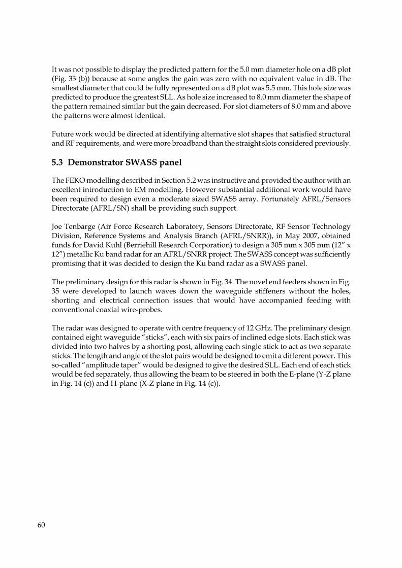
60
It was not possible to display the predicted pattern for the 5.0 mm diameter hole on a dB plot (Fig. 33 (b)) because at some angles the gain was zero with no equivalent value in dB. The smallest diameter that could be fully represented on a dB plot was 5.5 mm. This hole size was predicted to produce the greatest SLL. As hole size increased to 8.0 mm diameter the shape of the pattern remained similar but the gain decreased. For slot diameters of 8.0 mm and above the patterns were almost identical. Future work would be directed at identifying alternative slot shapes that satisfied structural and RF requirements, and were more broadband than the straight slots considered previously. 5.3 Demonstrator SWASS panel
The FEKO modelling described in Section 5.2 was instructive and provided the author with an excellent introduction to EM modelling. However substantial additional work would have been required to design even a moderate sized SWASS array. Fortunately AFRL/Sensors Directorate (AFRL/SN) shall be providing such support. Joe Tenbarge (Air Force Research Laboratory, Sensors Directorate, RF Sensor Technology Division, Reference Systems and Analysis Branch (AFRL/SNRR)), in May 2007, obtained funds for David Kuhl (Berriehill Research Corporation) to design a 305 mm x 305 mm (12” x 12”) metallic Ku band radar for an AFRL/SNRR project. The SWASS concept was sufficiently promising that it was decided to design the Ku band radar as a SWASS panel. The preliminary design for this radar is shown in Fig. 34. The novel end feeders shown in Fig. 35 were developed to launch waves down the waveguide stiffeners without the holes, shorting and electrical connection issues that would have accompanied feeding with conventional coaxial wire-probes. The radar was designed to operate with centre frequency of 12 GHz. The preliminary design contained eight waveguide “sticks”, each with six pairs of inclined edge slots. Each stick was divided into two halves by a shorting post, allowing each single stick to act as two separate sticks. The length and angle of the slot pairs would be designed to emit a different power. This so-called “amplitude taper” would be designed to give the desired SLL. Each end of each stick would be fed separately, thus allowing the beam to be steered in both the E-plane (Y-Z plane in Fig. 14 (c)) and H-plane (X-Z plane in Fig. 14 (c)).

DSTO-TR-2096
61
Figure 34: Preliminary design of a SWASS, Ku band radar, panel
Figure 35: Details of the waveguide end-launcher

62
6. Experimental Program
6.1 Introduction
A building-block test program was conceived to validate the SWASS concept. This program was focused on designing, manufacturing and testing the 305 mm x 305 mm (12” x 12”) SWASS panel containing a Ku band radar as described in Section 5.3. The planned test program is shown in Table 8. At the time of completion of the DSF, only the RF tests had been conducted on ten un-slotted waveguides. Further RF tests are required on other un-slotted waveguides before the waveguide material can be finalised. Additional coupon specimens are then planned to evaluate the effects of one, then multiple, slot(s) on the mechanical behaviour of, and radiation patterns from, waveguides manufactured from the optimal material. Finally, a smaller number of RF and mechanical tests will be conducted on the full-scale SWASS radars (structural element specimens) to validate the predictions made by EM modelling and structural analysis. 6.2 Specimens
6.2.1 Fibres
Two basic classes of CFRP material were evaluated. The first class consisted of one material, AS4/3501-6, a conventional aerospace grade pre-impregnated (prepreg) unidirectional tape. Table 8: The building-block test program that will be used to validate the SWASS concept
Test type
Specimen type Class of test Type of test Purpose
RF S-parameter Identify suitable waveguide materials Waveguide
– No slots Mechanical Axial compression Baseline mechanical property
RF Radiation pattern
Validate predicted radiation pattern for selected slot size/shape/location Waveguide
- Single slot Mechanical Axial
compression Establish effect of selected slots on a critical mechanical property
Coupon
Waveguide - Multiple
slots RF Radiation
pattern Validate predicted radiation pattern of slotted stick
RF Radiation pattern
Validate models pattern from a demonstrator SWASS
Axial compression
Struct-ural
element
Multi-stick array -
(SWASS demonstrat-
or) Mechanical In-plane
shear
Establish effect of slots on critical mechanical properties for the demonstrator SWASS

DSTO-TR-2096
63
The second class consisted of four different types of dry fibre fabrics that were consolidated using epoxy resin in liquid or film form. The dry fibres in these fabrics were 6k T650 carbon fibre tows braided into unidirectional fabrics. The 6k tows in these fabrics were oriented in the 0° direction and were held in place by 1k carbon tows oriented at ±45°. The 6k tows were either: (i) uncoated designation 6k T650, or coated with (ii) 20 wt % Cu then 10 wt % Ni designation 6/20/10, (iii) 40 wt % Cu then 10 wt % Ni designation 6/40/10, or (iv) 50 wt % Ni designation 6/50. 6.2.2 Resin and consolidation technique
The prepreg tape was pre-impregnated with 3501-6 resin and used in the as-received condition. These specimens were laid-up then cured either in an autoclave using the manufacturers recommended cure cycle or in an oven under vacuum. Most specimens manufactured from the dry fibres were infiltrated with liquid Epon 862 resin with 26.4 wt % Epicure Curing Agent W. Early specimens were prepared using the conventional liquid moulding techniques of Vacuum Assisted Resin Transfer Moulding (VARTM) or Resin Transfer Moulding (RTM). Latter specimens were prepared using prepreg that had been manufactured in-house. To manufacture this prepreg, liquid Epon 862 resin was firstly heated to 71 °C (160 °F) and degassed for 15 - 30 minutes. The weight of resin necessary to give a desired fibre volume fraction was metered onto the dry fabric. Finally the wetted fabric was staged in an autoclave at 689 kPa (100 psi) and 93 °C (200 °F) for a controlled time. The pressure ensured a uniform minimum thickness of the prepreg and the temperature/time were selected to leave a tacky, but workable, resin. The resulting prepreg was laid-up using the conventional prepreg lay-up technique and cured in the autoclave. 10 wt % of Pyrograf III (PR-24-LHT-XT) nano-fibres was added to the Epon 862 resin and this resin was formed into 0.076 mm (0.003”) or 0.178 mm (0.007”) thick films. Some specimens were manufactured with this material then consolidated using Resin Film Infusion (RFI). This resin did not appear to flow well so for some specimens the nano-reinforced film was used to line the inner face of the waveguide and liquid Epon 862 added to the outer face to ensure complete wetting out of the fibres. 6.2.3 Specimen types
The coupon level specimens were waveguide sticks with a nominal internal cross-section of 22.86 mm x 10.16 mm and lengths ranging from 200 mm to 350 mm. All waveguide sticks were cut to length using a diamond saw with no lubricant. RF tests were conducted on these specimens in the un-slotted condition. The RF tests required that standard WR-90 waveguide flanges be bonded onto the ends of the waveguide sticks. To do this the following procedure was followed. A small continuous bead of conductive epoxy resin (EG8020, AI Technology, 70 Washington Rd, Princeton Jct., NJ 08550, http://www.aitechnology.com) was metered around the mating surface of a UG 135-U MB waveguide flange using a wooden spatula. This flange was slid over the 22.8 mm x 10.1

64
mm (0.9” x 0.4”) section of a 22.8 mm x 10.1 mm x 25.4 mm (0.9” x 0.4” x 1”) aluminium aligning block that had been fastened to a flat base-plate. This block was used to maintain alignment of the stick and flange while the adhesive cured. The waveguide stick was slid over the aligning block until it pressed onto the conductive resin and made a positive connection with the mating surface of the flange. It was found that the EG8020 adhesive was compliant when cured so a thick continuous bead of cyanoacrylate adhesive (M-Bond 200) was then overlaid over the fillet between the waveguide and flange. The cyanoacrylate was allowed to cure overnight. The waveguide stick and flange were slid off the aligning block after curing. Removal sometimes required a moderate amount of prising and took some time because conductive adhesive was sometimes extruded into the waveguide section and partially bonded to the aligning block. Any conductive adhesive that remained on the inner wall of the waveguide was abraded off using coarse then medium grade sanding sticks. Abrading was continued until there was a smooth, debris-free, transition between the flange and waveguide. The flange installation procedure was repeated at the opposite end of the waveguide stick. 6.2.4 Testing
6.2.4.1 Un-slotted waveguides The first series of RF tests were used to establish whether any of the materials were suitable as waveguides. A TE10 wave was launched in the CFRP waveguides by connecting the output port of a HP 8510 Vector Network Analyser to the waveguide, through a coaxial cable, SMA-to-WR90 adaptor and short section of metallic WR-90 waveguide. The transmitted signal was analysed by connecting the opposite end of the CFRP waveguide to the input port of the Vector Network Analyser (VNA) using a similar series of components (waveguide section, adaptor, cable). The experimental setup is shown in Fig. 36. The insertion (S12) and return (S11) loss parameters for ten CFRP waveguides were measured over the operating frequencies of WR-90 waveguides, 7 – 12 GHz. The insertion losses are plotted in Fig. 37 and values at 10 GHz tabulated in Table 9. Figure 37 also shows the predicted attenuation due to conductor loss as defined by Equation 8 [23]. The conductivity for each set of waveguide data was calculated by conducting a least squares best fit between the experimental results and Equation 8.
( )2323 2 kab
kbaRs
c += πηβ
α (8)
Where: cα = Attenuation due to conductor loss for the TE10 mode (Np m-1)
sR = Wall surface resistance (Ω) = σμπ 0f
σ = Conductivity (S m-1) a = Waveguide broad-wall width (m)

DSTO-TR-2096
65
Figure 36: Experimental setup for measuring insertion and return loss of un-slotted waveguides b = Waveguide narrow-wall width (m)
β = Propagation constant (m-1) = 2
2 ⎟⎠⎞
⎜⎝⎛−
ank π
k = Wavenumber = 002 μεπf n = number of half-wave loops across the width of the waveguide = 1 for TE10
propagation mode 6.2.5 Results and discussion
Metal lined waveguides
As expected the standard metallic waveguide had the lowest insertion loss at only 0.0006 dB cm-1. The loss for an AS4/3501-6 waveguide lined with aluminium foil (DSF1301) was five times greater than that of the metallic waveguide, however with an insertion loss of 0.003 dB cm-1 it was still considered to be a reasonable waveguide. The losses in this waveguide were consistent with the attenuation due to conductor loss with

DSTO
-TR-2096
66
Figure 37: Measured insertion losses for CFRP waveguides and predicted attenuation due to conductor loss (Alpha_c) for the specified conductivity
(sigma)
0.00
0.05
0.10
0.15
0.20
0.25
0.30
0.35
0.40
0.45
0.50
7.0 7.5 8.0 8.5 9.0 9.5 10.0 10.5 11.0 11.5 12.0
Frequency (GHz)
Inse
rtio
n lo
ss (d
B/cm
)
DSF1301 Al lined AS4/3501-6Alpha_c (dB/cm) at sigma (S/m) of 11,200,000DSF1201 AS4/3501-6 [90 0]DSF1001 AS4/3501-6 [0 90]DSF0302 AS4/3501-6 [+45 -45]Alpha_c (dB/cm) at sigma (S/m) of 27,500DSF0601 6kC / Epon862Alpha_c (dB/cm) at sigma (S/m) of 2,600DSF0502 6kC+50%Ni / Epon862Alpha_c (dB/cm) at sigma (S/m) of 1,900DSF0403 6kC+40%Cu+10%Ni / Epon862+10%nano-fibreDSF0901 6kC+40%Cu+10%Ni / Epon862+10%nano-fibreDSF1101 6kC+40%Cu+10%Ni / Epon862+10%nano-fibreDSF0501 6kC+20%Cu+10%Ni / Epon862+10%nano-fibreAlpha_c (dB/cm) at sigma (S/m) of 1,500

DSTO-TR-2096
67
Table 9: Insertion loss of un-slotted waveguides at 10 GHz
Specimen ID Class Material
Insertion loss (dB
cm-1) Reference Standard metallic WR-90 waveguide 0.0006
DSF1301 Metal lined Aluminium lined AS4/3501-6 0.003 DSF1201 AS4/3501-6 [90 0]s lay-up 0.048 DSF1001 [0 90]s lay-up 0.050 DSF0302
Standard aerospace prepreg tape
[±45]s lay-up 0.061
DSF0601 Braided standard
carbon fibres/Standard resin
6k T650 braided fabric/Epon 862 0.157
DSF0502 Braided metal coated
carbon fibres/Standard resin
6/50 C/Ni braided fabric/Epon 862 0.167
DSF0403 6/40/10 C/Cu/Ni braided fabric/ Epon 862 0.168
DSF0901 6/40/10 C/Cu/Ni braided fabric/ 0.007” nano-fibre filled Epon 862 film 0.194
DSF1101 6/40/10 C/Cu/Ni braided fabric/ 0.007” nano-fibre filled Epon 862 film 0.219
DSF0501
Braided metal coated carbon fibres/Standard resin containing 10 wt
% PR-24-LHT-XT nano-fibres
6/20/10 C/Cu/Ni braided fabric/ 0.003” nano-fibre filled Epon 862 film 0.224
σ = 11.2 x 10⁶ S m-1. This conductivity is about one third that of aluminium (σAl = 38.0 x 10⁶ S m-1). One source of the larger loss was that the foil was not continuous around the walls of DSF1301. There was a seam, of less than 1 mm width, along the centreline of one broad-wall for the length of the specimen because the foil was not long enough to wrap fully around the mandrel. The seam increased the Ohmic resistance of that wall and thus losses. Overlapping the foil to ensure continuous contact was expected to reduce these losses, however this was not attempted because there was a risk that the thickness of an overlapping seam would lead to a reduction in fibre compaction pressure outside the overlap. The hard inner mandrel and outer tools would have prevented uniform compaction of the plies in the face containing the overlap. While a high-conductivity metal liner would enhance significantly the RF performance of a SWASS antenna, such a lining would introduce additional and possibly undesirable processing steps and inspection requirements. The costs of incorporating such linings can be justified in applications where ultimate performance is critical, such as space-based radars. The X-band antenna on the TerraSAR-X satellite used CFRP waveguides that were coated with silver [24]. In that application even the walls of the slots were metal coated. It is uncertain, but probably unlikely, that similar approaches could be justified for SWASS in aircraft.

DSTO-TR-2096
68
Highly conductive liners also increase the vulnerability of the structure to damage. If the SWASS were designed on the basis of an intact liner, then environmental degradation or damage due to events such as impact would degrade the liner and thus antenna performance, possibly substantially. Such structure would require inspection techniques that could identify damage and repair techniques that could restore conductivity. Both would add to through-life-support costs. Standard prepreg tape waveguides The results from the AS4/3501-6 unidirectional prepreg tape were very encouraging. The insertion losses of DSF[0302, 1001, 1201] were in the order of 0.5 dB m-1, corresponding to a loss of ≈ 12 % of the wave energy per metre, regardless of lay-up. The behaviour matched well that predicted for conductor loss with σ = 27.5 x 10³ S m-1. This conductivity is close to three orders of magnitude greater than the DC conductivity of CFRP. Further work is required to validate this measurement and explain the difference with DC conductivity. Given their high apparent conductivity and moderate insertion loss, it was judged that AS4/3501-6 prepreg tape would be acceptable for use as the first generation of SWASS waveguides. Uncoated or metal coated braided carbon fibres/unfilled epoxy The insertion losses in DSF0[502 and 601] were much greater than that of the specimens manufactured from AS4/3501-6 prepreg tape. The insertion loss in DSF0601 was consistent with attenuation due to conductor loss at σ = 2.6 x 10³ S m-1. In contrast the performance of DSF0502 did not match at all well the attenuation due to conductor loss. The measured losses were significantly higher at low frequency and lower at high frequencies. The three major differences between the materials in DSF0502, DSF0601 and the AS4/3501-6 prepreg tape waveguides, were (i) fibre architecture, (ii) fibre volume fraction, (iii) fibre coating, each of which is discussed below. DSF0[502 and 601] were manufactured from braided fabrics that contained 87 - 94 wt % (87 – 91 vol. %) carbon fibres in the axial direction and 5 - 11 wt % (7 – 11 vol. %) in the ±45° bias direction. The fabrics were considered unidirectional because most of the fibres were in the axial direction. One hypothesis to explain the high losses in these waveguide was that, during compaction and consolidation the bias tows restrained the axial tows and prevented them from flattening and contacting closely the adjacent axial tows. This would lead to relatively high conductivity within the individual axial tows but poor conductivity between adjacent tows. In contrast the prepreg tape contained no bias tows and the individual fibres were distributed uniformly across the cross-section of the ply, leaving much smaller gaps between adjacent fibres and improving the conductivity of the tape relative to the braided fabric. This argument is not supported by the results. Both DSF0502 and DSF0601 were braided, however only the performance of DSF0601 could be explained in terms of conductor loss. Thus it was concluded that the increased losses in DSF0[502 and601] were not caused by their braided architecture. Fibre volume fraction was significantly lower in the dry fabric specimens. The vacuum pressure under which they were compacted and consolidated was only sufficient to produce

DSTO-TR-2096
69
fibre volume fractions of 40 - 50 vol. % for DSF0[502 and 601], but 60 - 70 vol. % in the prepreg tape specimens. A lower fibre volume fraction was expected to reduce conductivity by increasing the distance between adjacent fibres. However, as with material architecture, both DSF0[502 and 601] would have had similar fibre volume fractions yet the performance of one was explained by considering conductor loss while the other was not. It was concluded that different fibre volume fraction was not likely to be the cause of performance differences. The final possibility was fibre coating. It was expected that carbon fibres coated with metal (nickel in the case of DSF0502) would be more conductive than untreated carbon fibres (DSF0601) and therefore produce waveguides with lower losses. This was clearly not the case. The metal coating was the only clear difference between DSF0502 and DSF0601 and is most likely the reason for the difference between the two specimens. It is hypothesised that the closely spaced, metal coated, carbon fibres interact with the RF waves, creating local inductive or capacitive circuits (complex impedance). This interaction was somewhat unexpected given the five and a half orders of magnitude difference between the length scales of these components. Carbon fibres are 7 μm diameter and λg ≈ 40 mm at 10 GHz. Further analysis is required to establish the mechanism of this interaction. Untreated or metal coated braided carbon fibres/nano-fibre filled epoxy Surprisingly, the specimens containing 10 wt % PR-24-LHT-XT nano-fibres in the Epon 862 epoxy resin behaved even more poorly than the waveguides manufactured from unfilled resin. Insertion losses ranged from very similar to that of the metal coated fibres in standard resin (DSF0502) at 0.168 dB cm-1 up to a very lossy 0.224 dB cm-1. The losses in these waveguides did not follow the attenuation due to conductor loss. Prior to testing it was expected that the nano-fibres would have provided conductive paths through the resin and into the structural carbon fibres. This should have improved the effective conductivity of the waveguide and therefore reduced insertion loss. Clearly this was not the case. Instead, the nano-fibres appear to have acted as absorbers. The literature has reported that nano-fibre filled resins can act as effective RF absorbers. It is possible that there will be particular configurations of nano-fibres, such as preferential alignments, that minimise losses in the RF currents. Substantial further work would be required to establish the nature of the interaction then develop techniques to exploit it in the SWASS waveguides. 6.3 Structural element
6.3.1 Tooling
A lay-up tool for the curing of structural element specimens was designed and machined. As shown in Fig. 38 the tool consisted of a Base Plate onto which were fastened a Fixed Restraining Bar and a Sliding Restraining Bar. The tool was large enough to prepare a 355 mm x 355 mm (14” a 14”) panel. The first step in laying-up a SWASS panel would be to lay-up the skin, if required, on the tool surface of the Base Plate and debulk it. Next, pre-wrapped and debulked waveguide mandrels

DSTO-TR-2096
70
Figure 38: Drawing of the SWASS panel lay-up tool would be placed on the Base Plate, the first mandrel being located along the corner between the Base Plate and Fixed Restraining Bar and subsequent mandrels packed against the most recently located mandrel. The desired specimen width would be created by packing the appropriate number of wrapped mandrels onto the Base Plate. If there was a gap between the last wrapped mandrel and the Sliding Restraining Bar then a spacer block would be required to fill it. Lateral pressure on the wrapped mandrels would be applied by the Sliding Restraining Bar. Threaded rods, passing between the Fixed and Sliding Restraining Bars
12” x 12”
14” x 14”
19” x 2” x 1” Fixed Restraining Bar
19” x 19” x ½” Base Plate
19” x 2 ½” x 1” Sliding Restraining Bar
2 off 26” x 1/2−20 threaded rods
9 off holes with 2” spacing to suit 3/8-24 x 1 ½” cap screw grade 8
with flat washers through Fixed
Restraining Bar. Tap thread through into
Base Plate to suit bolts
9 off 3/8” wide x 1” long slots with 2” spacing in Sliding Restraining Bar.
Tap thread into Base Plate to suit 3/8-24 x 1 ½” grade 8 cap screw,
through slots
14” = =
1.0”
2.0”
Tap for ½-20 threaded rod
Close clearance through-hole to suit
½” threaded rod
Blue lines constitute virtual layout of part
TOP VIEW
SIDE VIEW
END VIEW
DSTO-TR-2096
71
would be tightened to pull the Sliding Restraining Bar against the mandrels. Once the desired pressure/position had been achieved the Sliding Restraining Bar would be fastened to the Base Plate and the threaded rods removed. A second skin, if required, would be laid-up separately, debulked, then located on the stack of wrapped mandrels and debulked again. Finally, the tool with the laid-up part would be loaded into an autoclave and the part cured. No full-size structural element specimens were manufactured on this tool during the DSF. The tool was commissioned by manufacturing two 152 mm x 152 mm (6” x 6”) panels. These panels were prepared using the technique described in the previous paragraph except that the mandrels and skins were not debulked prior to placing on the tool. The quality of the cured parts were reasonable, however there were some wrinkles in the skins. It is most likely that these were caused by relative movement of the waveguides and skins during cure, and that debulking each part prior to assembly on the tool would have eliminated this problem. 6.4 Future work
It is planned that the remainder of the test program described in Table 8 be completed by the AFRL/VASA and DSTO teams in 2008.
7. Conferences and Training
7.1 Second Annual Advanced Signature Technology Symposium (ASTS)
7-9 November 2006, Dayton, Ohio The Symposium was held at the Air Force Institute of Technology (AFIT), located at WPAFB, and was sponsored by The Measurement And Signatures Intelligence (MASINT) Association and General Dynamics Information Technology (formerly Anteon Corp.), in cooperation with the Defense Intelligence Agency (DIA), National Signatures Program (NSP) and Wright Patterson MASINT Development Consortium. A major aim of the Symposium was to support the NSP. This is a joint, multi-agency, venture initiated by the DIA to meet increased customer demands for signature data. The NSP’s overarching goal is to facilitate access to high-quality signatures to a diverse customer base. The NSP leverages the full spectrum of signature related activities (initial collection, processing, development and detailed analysis) within the Department of Defense, intelligence community, industry and academia. The keynote speaker at the Symposium stated that the NSP was keen to expand signature collaboration with Commonwealth countries, however no details of any collaboration were given. The technical papers in the Symposium focused largely on terahertz and infrared radiation with an emphasis on the; creation of a database of reference signatures, interpretation of spectra and accounting for atmospheric effects. It is unlikely that this work will be applicable to CLAS or SWASS in the near to medium term because at the very high frequencies of these

DSTO-TR-2096
72
radiations the sensors are optical. It would be very difficult with existing technology to develop glass and crystal sensors, either load-bearing or strain tolerant, suitable for integration into airframe structure. The one Australian contribution to the Symposium was presented by FLTLT Samuel Harkiss, a RAAF Officer completing a Masters Degree at AFIT. His paper was titled “AFIT’s large commercial aircraft infrared signature tool (LCAIR)”. The tool consisted of a model of an aircraft (A340-300) and signature prediction algorithms. It is being refined by successive AFIT students under the supervision of Dr M. Marciniak. FLTLT Harkiss incorporated multiple bounce and bi-directional reflectance to the model although the improvements in accuracy offered by these additions were not quantified. 7.2 CONDS(W) Science Week
29 November – 1 December 2006, Washington, District of Columbia This excellent initiative by the Counsellor, Defence Science Washington (CONDS(W)) brought together all DSTO staff on long term attachment in North America for an annual meeting. It created a face-to-face link to DSTO, which appeared to be particularly useful for isolated staff. The major part of the program consisted of presentations by each of the posted staff describing their work program. A key theme emerging from these presentations was the wide range of work that DSTO supports. Attachments range from staff; working on specific platforms such as the Wedgetail Resident Project Team, fully integrated into organisations that transition technology directly into the military, to DSF’s undertaking more long range research. Most presenters also provided information regarding their experiences, personal situations and lessons learned. This too was very informative. A half day was used for briefings by Embassy of Australia staff and providing mandatory training to posted staff. The briefing by the policy section was a particular highlight. Its insights regarding the US system of government and culture explained many of the author’s experiences and observations both within AFRL and the greater United States. 7.3 FEKO Training Course
20-21 December 2006, Hampton, Virginia The first half day describing the theory of electromagnetism and the basis for the Method of Moments (MoM) solution to Maxwells Equations. The remaining one and a half days were conducted at the keyboard with the participants performing tutorial problems of increasing complexity. This training provided an excellent overview of the capabilities of FEKO and allowed the author to commence EM modelling immediately after the course. The major advantages of FEKO over other commercially available EM software are its user-friendly graphical interface and multiple solvers. Although the primary solution technique is MoM, FEKO also contains Multilevel Fast Multipole Method (MLFMM), Uniform Theory of Diffraction (UTD) and Physical Optics (PO) solvers. This allows problems to be solved efficiently regardless of their electrical size.

DSTO-TR-2096
73
Extensive use was made of the excellent technical support provided by the course organisers, Electromagnetic Software and Systems (USA) Inc. (EMSS USA, Langley Research Park, 144 Research Drive, Hampton VA 23666, http://www.emssusa.com) upon completion of the course. Well over ten requests for information regarding EM modelling principles and using FEKO were made in January and February 2007. All were answered on the same day and, where appropriate, the responses contained detailed “how-to” instructions complete with screen-dumps from the appropriate FEKO worksheet annotated with instructions on what to do. This was an excellent resource and contributed strongly to good progress in EM modelling and the results presented in Section 5. 7.4 Fundamental Principles of Electronic Warfare
Association of Old Crows, 12-15 February 2007, Alexandria, Virginia This course focused more on the principles and underlying physics rather than the hardware used to implement it. In this sense the courses were of limited direct applicability to CLAS. However the high quality of the lectures and lecturer provided a valuable introduction to these topics and a framework within which the role of the antenna could be understood. This course was presented by David Adamy and consisted of 16 approximately 90 minute sessions. It followed the chapters from references [25, 26] and provided an excellent overview of the EW field. The topics covered were; threats, radio propagation, antennas, receivers, digital signals, EW processing, search, emitter location, radar characteristics, jamming, electronic protection in modern radar, decoys, chaff, corner reflectors, infrared and electro-optics considerations and EW simulation. A significant amount of the course had the participants solving practical problems on radio wave propagation, communication range, radar warning receivers, jamming and decoys. This hands-on approach greatly reinforced the presentation material. The calculations for these problems were simplified by using slide rules and nomograms that had been devised and supplied by the presenter. 7.5 Principles of Modern Radar
Georgia Institute of Technology, 23-27 April 2007, Las Vegas, Nevada This was an intensive course that consisted of 32 approximately one hour lectures. The lecture topics covered radar principles, systems, techniques, phenomenology and the basics of radar technology. Specific topics included antennas, transmitters, receivers, clutter and noise, detection, signal processing, waveform design, Doppler techniques, resolution, and multi-path and reflectivity measurements. As with the Fundamental Principles of EW course, this course focused more on signal processing than radar hardware and was therefore of limited direct applicability to the development of CLAS, however the insight this course gave to a field outside the author’s previous training was excellent.

DSTO-TR-2096
74
7.6 IEEE Antennas and Propagation Society International Symposium
11-15 June 2007, Honolulu, Hawaii The Technical Program for this conference was held over four days, with close to fifteen parallel sessions per day. Presenters represented the full spectrum of work in the field of antennas from fundamental and applied studies at universities and government laboratories, through to products from industrial suppliers. Clearly only a fraction of all presentations could be attended. The major themes of those sessions that were attended were the growing use of; meta-materials in antennas, radiofrequency identification (RFID) tag antennas and multiple input, multiple output (MIMO) devices. The topic of most direct relevance to CLAS was antenna miniaturisation through the use of meta-materials. Meta-materials are dielectric materials that contain dispersions, at the atomic- or nano-scale, of other materials such as magnetic particles or fibres. In this way it is possible to control the gross electrical and magnetic properties of the material, a very useful capability in the construction of antennas. In general meta-materials do not have sufficiently high stiffness and strength to act as load-bearing structure, however their mechanical properties are likely to be sufficient for them to be incorporated into CLAS. Possible applications for meta-materials would include substrates for microstrip antennas, windows for SWASS slots and wall liners for SWASS waveguides. A single paper was presented on the topic of CLAS [27]. This paper described tests conducted on probe-fed four element microstrip arrays embedded in flat and curved honeycomb sandwich panels. Each panel was damaged with the same energy from an instrumented drop-weight impact machine. It was found that the radiation pattern was strongly dependent on the curvature of the undamaged panel and that the extent of damage decreased as panel curvature increased. The effect of impact damage on radiation pattern was not reported. Short Courses were presented on the final day of the conference. The author attended “Miniaturization and material design methods for antennas”, presented by Professor J. Volakis, Dr C-C. Chen and S. Koulouridis of the Ohio State University (OSU). The highlight of the course was the session presented by C.-C. Chen, who clearly and succinctly described the fundamental principles of antenna operation, performance and miniaturisation. The subsequent sessions described the research performed at OSU applying these principles to reduce the size of antennas while maintaining acceptable performance.
8. Follow-on DSTO/AFRL Program
Both DSTO-AVD and AFRL/VASA were keen to continue the collaboration because of the success of the DSF and the promising potential of the SWASS concept. An attempt was made

DSTO-TR-2096
75
to create a bilateral agreement between DSTO and AFRL on this topic however the agreement did not progress beyond the AFRL International Affairs Office. As an alternative, a Collaborative Program (CP) has been proposed under The Technical Cooperation Program, Aerospace Systems Group, Technical Panel 4 - Structures and Dynamics of Air Vehicles, Key Technical Area 4B - Structural Design of Aerospace Systems (TTCP AER TP-4 KTA-4B). This proposal has received strong support from the USAF and Australian members on TTCP AER TP-4. The CP has been submitted and is awaiting approval. The aim of the proposed CP is to extend the work that was commenced during the DSF. A series of projects would be conducted to devise and validate concepts/approaches/techniques to increase further the SWASS design space. The following is a non-exhaustive list of features or desired capabilities that were proposed as the basis for selecting these projects;
increased bandwidth, increased gain, beam steering capability, control over beam width, optimized stiffener cross-section, increased tolerance to structural deformation, simplified feeding, reduced effect of slots on structural strength, and low-cost manufacture of precision dielectric-filled slots.
The selected concepts/approaches/techniques would be analysed using structural and electromagnetic modelling and promising predictions validated by testing at the coupon and structural element level.
9. Security Restrictions
The most significant limitation to additional progress during the DSF were the restrictions on access to facilities and information. Fortunately the relationship between the author and AFRL/VASA team was excellent and substantial progress was made in the development of CLAS technology while working within these limitations. The author had unescorted access to his office building and the WPAFB public access areas but an escort was required to enter the AFRL/VASA laboratory building. No access was granted to any other local facility, even those such as the AFRL/SN building that were directly applicable to the approved work program. A Request for Visit Authorisation process was required to gain access to any of these, or other, facilities. These restrictions did slow progress because a substantial part of the DSF work program required access to the composite manufacturing facilities housed in the AFRL/VASA laboratory building. The time and timing

DSTO-TR-2096
76
of work conducted in this building had to be coordinated with the escort. Not being permitted to enter the AFRL/SN building meant that staff from AFRL/SNRR and Berriehill Research Corporation were required to perform the electromagnetic testing. This diverted these staff from their planned work programs and limited the learning experience of the author. The access to information was substantially more restricted than access to facilities. No access was gained to any information that was not in the open literature or had not been expressly approved for foreign disclosure. This certainly limited the potential areas of interaction and probably some progress in this DSF because relevant lessons that the experienced AFRL/VASA team had learned in previous projects could not be disclosed. As indicated previously, despite the limitations on movement and information the author considers that the DSF was very successful. The author was co-located with the originators of the CLAS concept and new concepts were devised. One of these, SWASS, was selected for further development and is being patented by AFRL.
10. Conclusions
The author conducted a successful Defence Science Fellowship (DSF) on the topic of Conformal Load-bearing Antenna Structure (CLAS) with the Air Force Research Laboratory, Air Vehicles Directorate, Structures Division, Advanced Structural Concepts Branch (AFRL/VASA), Multifunctional Structures Team at the Wright Patterson Air Force Base, Ohio, USA, from June 2006 until August 2007. The aim of CLAS is to enhance the performance and capability of air vehicles by integrating antennas into the load-bearing airframe structure. The author and AFRL/VASA team devised a new CLAS concept, called Slotted Waveguide Antenna Stiffened Structure (SWASS), where the top-hat cross-section stiffeners commonly used to reinforce thin composite aircraft skins or blade stiffeners in sandwich panels also serve as slotted waveguide antennas. The concept was partially validated by modelling, design, manufacture and testing at the coupon level. AFRL is patenting this concept while work is continuing to complete the validation and establish a baseline capability. The DSF provided the author with the opportunity to work unencumbered by organisational responsibilities with the originators of the CLAS concept. This allowed him and AFRL/VASA team to devise a range of novel CLAS, and commence validation of the SWASS, concepts. Security restrictions limited further, potentially valuable, interactions and information exchanges.

DSTO-TR-2096
77
11. Acknowledgements
The author is grateful to DSTO for providing funding and selecting him to undertake the DSF. Bill Baron (AFRL/VASA) is thanked for answering the initial request for expressions-of-interest then acting as the US sponsor for the DSF. He, Jim Tuss (AFRL/VASA) and LT John-David de la Harpe (USAF) provided outstanding technical assistance, logistical support and friendship. They are largely responsible for the technical success of the DSF and the enjoyment that the author and his family experienced while in the US. Larry Mack (Selectek) is thanked for his ongoing support in the laboratory, particularly keeping the manufacturing facilities running, machining tooling and operating the autoclave. Caleb Gillespie joined the AFRL/VASA Team in June 2007 and was a great help in the laboratory. Joe Tenbarge (AFRL/SNRR) and Michael Corwin (AFRL/SNRR) are thanked for providing AFRL/SN support. The efforts of David Kuhl (Berriehill Research Corporation) in conducting the waveguide tests and commencing the design of the demonstrator SWASS panel are gratefully acknowledged. Finally, the contribution of Dr Kim Brown (DSTO - EWRD), a fellow DSF recipient also working at WPAFB, is acknowledged. His enthusiasm and understanding of electronic warfare contributed greatly to the creative process. He was largely responsible for initiating the proposal to install SWASS in an Aerosonde UAV as described in Section 4.
12. References
1. Air Force Research Laboratory, “Transforming the future of warfare with unmanned air vehicles”, AFRL Horizons Technical Articles Online, VA0209, September, 2002 http://www.afrlhorizons.com/Briefs/Sept02/VA0209.html
2. Callus, P. J., “Conformal load bearing antenna structure for Australian Defence Force aircraft”, DSTO Technical Report, DSTO-TR-1963, March, 2007, 40 pp.
3. Volakis, J., “A broadband VHF-L band cavity-backed slot spiral antenna”, AFRL-IF-RS-TR-2005-169, Air Force Research Laboratory, Information Directorate, Rome Research Site, 525 Brooks Rd, Rome, New York, May, 2005, 58 pp.
4. Volakis, J. L., Nurnberger, M. W. and Filipovic, D. S., “A broadband cavity-backed slot spiral antenna”, IEEE Antennas and Propagation magazine, Vol. 43, No. 6, December 2001, pp. 15-26
5. Schreider, L., Begaud, X., Soiron, M. and Perpere, B., “Archimedian microstip spiral antenna loaded by chip resistors inside substrate”, 2004 IEEE Antennas and Propagation Society International Symposium, Volume 1, Monterey, California, USA, 20-25 June 2004, pp. 1066-1069.

DSTO-TR-2096
78
6. Bhobe, A., Cencich, T., Burford, J., Filipovic, D., “Broadband dual-mode slot antenna”, 2003 Antenna Applications Symposium, Monticello, Illinois, USA, 17-19 September 2003, 13 pp.
7. Filipovic, D.S., Siah, E.S., Sertel, K., Liepa, V.V. and Volakis, J.L., “A thin broadband cavity-backed slot spiral antenna for automotive applications”, International Symposium of the IEEE Antennas and Propagation Society, Volume 1, Boston, Massachusetts, USA, 8-13 July, 2001, pp. 414-417.
8. Killen, W.D, Pike, R.T. and Delgado, H.J., “High efficiency slot fed microstrip antenna having an improved stub”, United States Patent 6,791,496 B1, 14 September 2004, 17 pp.
9. Rowe, W. and Ghorbani, K., “Investigation of conformal load-bearing antenna structures”, School of Electrical & Computer Engineering, RMIT University, Melbourne, Victoria, 3001, 30 March 2006, 30 March 2006, 9 pp.
10. Ando & Hirokawa Laboratory, “Crossed-Slot”, Animation, accessed 23 October 2006, http://www-antenna.ee.titech.ac.jp/research/animation-e.html
11. Marshall, T., “Unidirectional waveguide antennas”, accessed 23 October 2006, http://www.trevormarshall.com/waveguides.htm
12. Gosselin, R. B., “A computer-aided approach for designing edge-slot waveguide arrays”, 2003 Antenna Applications Symposium, Monticello, Illinois, USA, 17-19 September, 2003, 25. pp.
13. Heidari, A. A., Fofooraghi, K. and Hakkak, M., “Reducing resonant length of sidewall-inclined slots in a rectangular waveguide”, Microwave and Optical Technology Letters, Vol. 37, No. 3, 5 May 2003, pp. 222-226.
14. Solbach, K., “Below-resonant-length slot radiators for traveling-wave-array antennas”, IEEE Antennas and Propagation Magazine, Vol. 38, No. 1, February, 1996, pp. 7-14.
15. Banalis, C. A., “Antenna Theory”, Third Edition, John Wiley and Sons. Inc., 2005, 1099 pp.
16. Kruger, B. E., “Edge slotted waveguide antenna array with selectable radiation direction”, United States Patent, 4,229,745, 21 Oct 1980, 7 pp.
17. You, C.S., Hwang, W., Park, H.C., Lee, R.M., and Park, W.S., “Microstrip antenna for SAR application with composite sandwich construction: surface-antenna-structure demonstration”, Journal of Composite Materials, Vol. 37, No. 4, 2003, pp. 351-364.
18. Aerosonde Pty Ltd, Home web page, accessed 23 October 2006, http://www.aerosonde.com
19. Finn, A., Brown, K. and Lindsay, “Miniature UAV’s & future electronic warfare”, Land Warfare Conference, Brisbane, Australia, 22-24 October 2002, 13 pp. http://www.aerosonde.com/downloads/Aerosonde_DSTO_EW.pdf
20. Aerosonde Pty Ltd, “The Aerosonde system”, 4 pp. http://www.aerosonde.com/downloads/the_aerosonde_system.doc
21. Aerosonde Pty Ltd, “Aerosonde “Sting””, 2000pixels image, downloaded 23 October 2006, http://www.aerosonde.com/images/upload/1597563953_aero_black_2000.jpg
22. Aerosonde Pty Ltd, “Aerosonde “3view””, A4 format 300dpi image, downloaded 23 October 2006, http://www.aerosonde.com/images/upload/950769439_aerosonde_3vu_2004_300dpi.jpg
23. Pozar, D. “Microwave Engineering”, Third Edition, John Wiley and Sons, 2005, 700 pp.

DSTO-TR-2096
79
24. Stangl, M., Werninghaus, R. and Zahn, R., “The TerraSAR-X active phased array antenna”, IEEE Int. Symp. on Phased Array Systems and Technology, 14-17 October, 2003, pp. 70-75.
25. Adamy, D, “EW101: A first course in electronic warfare”, Artech House Inc., 685 Canton St, Norwood, Massachussets, USA, 2001, 308 pp.
26. Adamy, D., “EW102: A second course in electronic warfare”, Artech House Inc., 685 Canton St, Norwood, Massachussets, USA, 2004, 274 pp.
27. You, C., Hwang, W. and Tentzeris, M. M., “Impact behaviour and radiation performance of a structurally integrated antenna array conformed around cylindrical bodies”, IEEE- Antennas and Propagation Society (AP-S) International Symposium, Paper 965, Honolulu, Hawaii, USA, 11-15 June 2007, pp. 3844-3847.

DSTO
-TR-2096
80
Appendix A: Test Specimen Manufacture Details
The test specimens manufactured during the DSF are described in Table A.1 and the attendant notes at the foot of this table. Table A1: Specimen material, manufacture and test details
Run Manufacture Date
Specimen ID Type1 Fibre2 Fibre
Form3 Lay-up4 Resin5 Manufacture
Technique6 Mandrel Number7
Outer Tool8
Cure Cycle9 Test10
DSF01 8/2/07 DSF0101 1 1 1 1 1 1 0 1 1 1 DSF02 1/3/07 DSF0201 1 1 1 1 1 1 1 2 1 1
DSF0301 1 1 1 1 1 1 1 3 2 1 DSF03 20/3/07 DSF0302 1 1 1 1 1 1 2 2 2 2 DSF0401 1 2 2 2 2 2 1 3 2 1 DSF0402 1 3 2 2 2 2 2 3 2 1 DSF0403 1 4 2 2 2 2 3 3 2 2 DSF0404 1 5 2 2 2 2 4 3 2 1 DSF0405 2 2 2 3 2 2 99 2 2 1 DSF0406 2 2 2 4 2 2 99 2 2 1 DSF0407 2 2 2 5 2 2 99 2 2 1 DSF0408 2 3 2 3 2 2 99 2 2 1 DSF0409 2 3 2 4 2 2 99 2 2 1 DSF0410 2 3 2 5 2 2 99 2 2 1 DSF0411 2 4 2 3 2 2 99 2 2 1 DSF0412 2 4 2 4 2 2 99 2 2 1 DSF0413 2 4 2 5 2 2 99 2 2 1 DSF0414 2 5 2 3 2 2 99 2 2 1 DSF0415 2 5 2 4 2 2 99 2 2 1
DSF04 11/4/07
DSF0416 2 5 2 5 2 2 99 2 2 1 DSF0501 1 3 2 2 2 2 5 3 2 2 DSF05 23/5/07 DSF0502 1 5 2 2 3 3 4a 4 2 2
DSF06 29/6/07 DSF0601 1 2 2 2 4 4 5 5 3 2

DSTO
-TR-2096 81
Run Manufacture Date
Specimen ID Type1 Fibre2 Fibre
Form3 Lay-up4 Resin5 Manufacture
Technique6 Mandrel Number7
Outer Tool8
Cure Cycle9 Test10
DSF07 28/6/07 DSF0701 1 1 1 4 1 1 4 3 1 1 DSF0801 2 2 2 3 5 2 99 2 1 1 DSF0802 2 3 2 3 5 2 99 2 1 1 DSF0803 2 4 2 3 5 2 99 2 1 1 DSF08 2/7/07
DSF0804 2 5 2 3 5 2 99 2 1 1 DSF09 3/7/07 DSF0901 1 4 2 6 5 2 6 6 1 2 DSF10 3/7/07 DSF1001 1 1 1 4 1 1 8 6 1 2 DSF11 9/7/01 DSF1101 1 4 2 2 5 + 3 4 6 5 3 2 DSF12 5/7/07 DSF1201 1 1 1 7 1 1 7 6 1 2 DSF13 9/7/07 DSF1301 1 1 1 8 1 1 8 6 1 2
DSF1401 1 5 3 2 3 1 6 7 1 1 17/7/07 DSF1402 1 5 4 2 3 1 7 7 1 1 DSF1403 1 5 5 2 3 1 8 7 1 1 DSF14
19/7/07 DSF1404 1 5 6 2 3 1 ? 8 1 1 DSF1501 1 1 1 1 1 1 1a 7 1 1 DSF15 19/7/07 DSF1502 1 1 1 1 1 1 2a 7 1 1 DSF1601 2 Nil N/A N/A 5 2 99 2 1 1 DSF1602 2 5 2 4 5 2 99 2 1 1 DSF1603 2 5 2 9 5 2 99 2 1 1 DSF16 19/7/07
DSF1604 2 5 2 9 5 2 99 2 1 1 DSF1701 1 1 1 1 1 1 3a 7 1 1 DSF17 20/7/07 DSF1702 1 1 1 1 1 1 2b 7 1 1
DSF18 23/7/07 DSF18[1-23] 3 2-5 2 9 3 5 99 9 4 1
DSF19 26/7/07 DSF19 3 4 7 9 3 5 99 9 5 1 DSF20 30/7/07 DSF20 3 2-5 8 9 3 5 99 9 6 1 DSF21 1/8/07 DSF21 3 3-5 8 9 3 5 99 9 7 1
DSF2201 1 1 1 1 1 1 9 9 4 3 DSF22 1/8/07 DSF2202 2 1 1 4 1 1 99 2 4 3

DSTO
-TR-2096
82
Run Manufacture Date
Specimen ID Type1 Fibre2 Fibre
Form3 Lay-up4 Resin5 Manufacture
Technique6 Mandrel Number7
Outer Tool8
Cure Cycle9 Test10
DSF2203 2 4 DSF19 4 3 1 99 2 4 3 DSF2301 1 2 DSF20 10 6 1 3a 7 4 1 DSF2302 1 3 DSF24 10 6 1 1b 7 4 1 DSF2303 1 5 DSF25 10 6 1 2b 7 4 1 DSF2304 1 4 DSF25 10 6 1 9 7 4 1
DSF23
DSF2305 1 3 DSF25 10 6 1 5a 7 4 1 DSF24 3/8/07 DSF24 3 3 8 9 3 5 99 9 8 1 DSF25 8/8/07 DSF25 3 3-5 8 9 3 5 99 9 8 1
DSF2601 1 1 1 1 1 1 10 7 4 4 DSF2602 1 1 1 1 1 1 14 7 4 4 DSF26 14/8/07 DSF2603 1 1 1 1 1 1 17 7 4 4 DSF2701 1 1 1 1 1 1 11 7 4 4 DSF2702 1 1 1 1 1 1 12 7 4 4 DSF2703 1 1 1 1 1 1 15 7 4 4 DSF27 17/8/07
DSF2704 1 1 1 1 1 1 16 7 4 4 DSF2801 4 1 1 11 1 1 20-25 10 4 1 DSF28 23/8/07 DSF2802 5 1 1 11 1 1 26-31 10 4 1
Notes: 1 Type
1 Fibres (prepreg or dry) laid-up around an aluminium mandrel 2 Flat part 3 In-house prepreg 4 SWASS panel. Fibres laid-up around mandrels. Broad-walls butted together. Inner and outer skins 5 SWASS panel. Fibres laid-up around mandrels. Narrow-walls butted together. Inner and outer skins

DSTO-TR-2096
83
2 Fibre 1 AS4 Hexcel AS4/3501-6, 35 %, 150 AW, 12” tape, Date of
Manufacture: 7 Nov 2001, Lot: P2106-4 2 6/C 6k T650 carbon fibres braided by A&P Technology such that 6k
fibres were in 0° direction and held in place by 1 k carbon tows at ±45°
3 6/20/10 C/Cu/Ni 6k T650 carbon coated by Diamond Fibre with 20 wt % Cu then 10 wt % Ni. Fibres resized. Fibres braided by A&P Technology such that metal coated fibres were in 0° direction and held in place by 1 k carbon tows at ±45°
4 6/40/10 C/Cu/Ni 6k T650 carbon coated by Diamond Fibre with 40 wt % Cu then 10 wt % Ni. Fibres resized. Fibres braided by A&P Technology such that metal coated fibres were in 0° direction and held in place by 1 k carbon tows at ±45°
5 6/50 C/Ni 6k T650 carbon coated by Diamond Fibre with 50 wt % Ni. Fibres resized. Fibres braided by A&P Technology such that metal coated fibres were in 0° direction and held in place by 1 k carbon tows at ±45°
3 Fibre Form
1 Prepreg tape 2 Dry fibre braided fabric 3 Dry fibre braided fabric infused with liquid resin for Vf = 50 vol. % 4 Dry fibre braided fabric infused with liquid resin for Vf = 33 vol. % 5 Dry fibre braided fabric infused with liquid resin for Vf = 25 vol. % 6 Dry fibre braided fabric infused with liquid resin for Vf = 20 vol. % 7 Dry fibre braided fabric infused with liquid resin for Vf = 56 vol. % 8 Dry fibre braided fabric infused with liquid resin for Vf = 45 vol. %
4 Lay-up 1 [45 -45]s 2 [0 90] 3 [0]4 4 [0 90]s 5 [45 0 -45 90]s 6 [90 0] 7 [90 0]s 8 [Aluminium foil ±452] 9 [0] 10 [45 -45] 11 Waveguides [45 -45], skins [90 0]s
5 Resin 1 3501-6 as prepreg with fibre

DSTO-TR-2096
84
2 0.003” thick sheet of Epon 862 + 10 % #94 (University of Dayton Research Institute (UDRI) designation for Pyrograf III (PR-24-LHT-XT) nano-fibres). Film manufactured by UDRI in Jan/Feb 2007
3 Epon 862 as liquid with 26.4 wt % Epi-cure Curing Agent W 4 Epon 862 as liquid with 13.5 wt % Epi-cure Curing Agent W 5 0.007” thick sheet of Epon 862 + 10 % #94 (UDRI designation for Pyrograf III (PR-24-
LHT-XT) nano-fibres). Film manufactured by UDRI on 29 June 2007 6 No additional resin used. Resin contained in in-house prepreg
6 Manufacture Technique 1 Prepreg lay-up 2 Resin Film Infusion (RFI) 3 Vacuum Assisted Resin Transfer Moulding (VARTM) 4 Resin Transfer Moulding (RTM) 5 Meter resin onto dry fibre then stage in an autoclave
7 Mandrel Number 0 As-received 25.4 mm x 12.7 mm aluminium extrusion cut to 360 mm length 1 305 mm x 25.4 mm x 12.7 mm aluminium extrusion machined to nominal 22.784 mm x
10.135 mm (0.897” x 0.399”) section. Sharp edges broken but not rounded 1a Mandrel 1 wrapped with two plies of “super slick” Teflon tape (Saint Gobain, R253, 2” x
18 yards, Lot 207043) 1b Mandrel 1 wrapped with one ply of “super slick” Teflon tape (Saint Gobain, R253, 2” x
18 yards, Lot 207043) 2 305 mm x 25.4 mm x 12.7 mm aluminium extrusion machined to nominal 22.784 mm x
10.135 mm (0.897” x 0.399”) section. Sharp edges broken but not rounded 2a Mandrel 2 wrapped with three plies of “super slick” Teflon tape (Saint Gobain, R253, 2”
x 18 yards, Lot 207043) 2b Mandrel 2 wrapped with one ply of Teflon tape (2255-2, 3” x 18 yards, Lot 7070116) 3 305 mm x 25.4 mm x 12.7 mm aluminium extrusion machined to nominal 22.784 mm x
10.135 mm (0.897” x 0.399”) section. Sharp edges broken but not rounded 3a Mandrel 3 wrapped with one ply of “super slick” Teflon tape (Saint Gobain, R253, 2” x
18 yards, Lot 207043) 4 305 mm x 25.4 mm x 12.7 mm aluminium extrusion machined to nominal 22.784 mm x
10.135 mm (0.897” x 0.399”) section. Sharp edges broken but not rounded 4.a Mandrel 4 with 0.8 mm (1/32”) radius along all edges 5 355 mm x 25.4 mm x 12.7 mm aluminium extrusion machined to taper. Nominal small
end 22.657 mm x 10.008 mm (0.892” x 0.394”) and large end 22.911 mm x 10.262 mm (0.902” x 0.404”). 0.8 mm (1/32”) radius along all edges
5a Mandrel 5 wrapped with one ply of “super slick” Teflon tape (Saint Gobain, R253, 2” x 18 yards, Lot 207043)
6 Tapered mandrel. Length: 355 mm, Large end: 22.87 mm x 10.22 mm, Small end: 22.48 x 10.06 mm
7 Tapered mandrel. Length: 355 mm, Large end: 22.87 mm x 10.22 mm, Small end: 22.48 x 10.06 mm
8 Tapered mandrel. Length: 355 mm, Large end: 22.87 mm x 10.22 mm, Small end: 22.48 x 10.06 mm

DSTO-TR-2096
85
9 Parallel mandrel (Length: 355 mm, End 1: 22.68 mm x 10.04 mm, End 2: 22.73 mm x 10.03 mm) with one ply of “super slick” Teflon tape
10-42 Parallel mandrel (406 mm x 22.54 mm x 9.86 mm) with one ply “super slick” Teflon tape. Final outside dimension 22.78 mm x 10.10 mm
99 Flat caul plate 8 Outer Tool 1 Peel ply, non-perforated Teflon, breather cloth, bagging film 2 Non-porous (glass filled) Teflon, breather cloth, bagging film 3 Floating, 305 mm long, machined aluminium “L” cross-section (long leg 22 mm wide,
short leg 10 mm wide) hard outer moulds directly against part 4 Dry fibres wrapped with two layers of VARTM resin dispersion media (stretchable
diamond shaped pattern). Floating, machined aluminium “L” shaped (long leg 22 mm wide, short leg 10 mm wide) floating hard outer moulds located against dispersion media
5 RTM mould. 16 mm thick aluminium plates fastened together to fully enclose perform. Hard end-caps fastened to mould and flanges of vacuum inlet and outlet ports
6 Floating, 305 mm long, machined aluminium “L” cross-section (long leg 22 mm wide, short leg 10 mm wide) hard outer moulds. Flash tape along faces directly against part
7 Floating, 305 mm long, machined aluminium “L” cross-section (long leg 22 mm wide, short leg 10 mm wide) hard outer moulds. Single ply of non-perforated Teflon between part and tool taped to one tool and pulled taut.
8 Floating, 305 mm long, machined aluminium “L” cross-section (long leg 22 mm wide, short leg 10 mm wide) hard outer moulds. Single ply of bagging film between part and tool
9 Non-porous (glass filled) Teflon, aluminium caul plate, breather cloth, bagging film 10 SWASS panel lay-up tool 9 Cure Cycle 1 Vacuum oven. Tambient (≈3°F min-1) → 350 °F (hold 2 h) → Tambient (oven cool). Maintain
vacuum throughout cure 2 Autoclave cure
Tambient (heat at 1.5 °F min-1, full vacuum, 50 psi) → 240 °F (vent vacuum) → 350 °F (heat at 3.7°F min-1 while ramping pressure from 50-100 psi, hold 1 h at 350 °F and 100 psi) → 150 °F (cool to 150 °F while maintaining 100 psi then vent) → Tambient
3 Oven. Tambient (≈3°F min-1) → 350 °F (hold 2 h) → Tambient (oven cool). Part vented to atmosphere throughout cure
4 Autoclave cure Tambient (heat at 3-5 °F min-1, full vacuum on part, increase chamber pressure to 85 psi) → 240 °F then hold 1 h → 350 °F (heat at 3-5 °F min-1 with vacuum on part. Increase pressure in chamber to 100 psi). Hold 2 h at 350 °F → cool at 3-5 °F min-1 to 150 °F while maintaining 100 psi in chamber

DSTO-TR-2096
86
→ vent vacuum on part and chamber at 150 °F → Tambient
5 Autoclave staging Tambient (heat at 3-5 °F min-1, full vacuum on part, increase chamber pressure to 100 psi) → 200 °F (hold 2 h 25 min) → Vent part and chamber to atmosphere then cool at 3-5 °F min-1 → Tambient
6 Autoclave staging Tambient (heat at 3-5 °F min-1, full vacuum on part, increase chamber pressure to 100 psi) → 200 °F (hold 1 h 40 min) → Vent part and chamber to atmosphere then cool at 3-5 °F min-1 → Tambient
7 Autoclave staging Tambient (heat at 3-5 °F min-1, full vacuum on part, increase chamber pressure to 100 psi) → 200 °F (hold 1 h 30 min) → Vent part and chamber to atmosphere then cool at 3-5 °F min-1 → Tambient
8 Autoclave staging Tambient (heat at 3-5 °F min-1, full vacuum on part, increase chamber pressure to 100 psi) → 200 °F (hold 45 min) → Vent part and chamber to atmosphere then cool at 3-5 °F min-1 → Tambient
10 Test 1 Not tested 2 Flanges bonded to ends then S-parameters (S11, S21) measured in RASCAL 3 Through-panel transmission loss 4 Slots to be milled in one narrow wall. Flanges to be bonded to ends. S-parameters to be
measured in RASCAL The following notes describe each of the manufacturing trials and the lessons learned from each. DSF 01 Approach Wrapped prepreg tape around oversize mandrel using ruler for
assistance. Oven cured under vacuum. Comments Very difficult to use out-of-date prepreg. Material was stiff in the fibre
direction, brittle transverse to fibre direction and had nil tack. Any transverse tension, which was unavoidable given the ±45° lay-up, caused ply splitting.
Inspection Part appeared reasonable but peel ply was thoroughly embedded into part and had to be removed by abrading.

DSTO-TR-2096
87
Lessons Learned Manufacture of waveguides is feasible. Do not use peel ply.
DSF02 Approach Wrapped prepreg tape around correct size mandrel using ruler and hot-
air gun. Wrapped with porous Teflon and oven cured under vacuum. Comments Prepreg was still very difficult to work without suitable tooling.
Effectiveness of hot-air gun was questionable. The temperature at which the prepreg softened and gained some tack, but did not fall apart, was very difficult to maintain.
Inspection Smooth outer skin but the inner surface did not follow the mandrel along the corners and the outer surface bunched along the corners.
Lessons Learned Hot-air gun was not practicable for material in this condition. Require a more effective technique to press the fibre against the mandrel.
DSF03 Approach Wrapped prepreg over mandrel using an “L” section hard outer tooling.
Cured in autoclave, one specimen under hard tool and one under vacuum bag.
Comments Although working with the prepreg was still difficult, it was much easier to get it to conform to the mandrel without bunching along the corners when using the hard outer tool.
Inspection Specimen cured under hard tool appeared good. Inner surfaces contacted mandrel even along the corners and outer surfaces were flat with no bunching along the corners. Specimen cured under vacuum bag was poor. Inner surfaces were not flat near the corners and one outer face had bunched.
Lessons Learned The hard tool was very useful during lay-up and was required during curing even when using the autoclave.
DSF04 Approach Wrapped metal coated carbon fibre fabric and nano-fibre reinforced
resin film over mandrels. Hard outer tools. Autoclave cured. Comments Lay-up of inner 0° ply was very easy but outer 90° ply was very difficult.
Resin film assisted to hold fibres in position, but plies were still very difficult to position. Cutting plies to final size was extremely difficult.
Inspection Resin did not appear to flow nor cure properly. Very flaky and brittle and not wetting fibres. Mandrels needed to be hammered to remove them from the specimens. Surface finish was good except along corners where hard tools did not contact. Resin and fibres bunched along these edges.
Lessons Learned Need new resin film. Desirable to redesign hard outer tools to minimise the gap along the two edges where the tool overlapped.

DSTO-TR-2096
88
DSF05 Approach For first specimen, wrap metal coated carbon fibres over a parallel sided
mandrel and retain using two layers of diamond pattern resin dispersion media. VARTM infuse. Break out from vacuum bag, add hard outer tools, re-bag and cure in autoclave. For second specimen repeat DSF04 but use tapered mandrel.
Comments Very difficult to hold dry fibres in position, especially outer 90° ply, when not using resin film. VARTM appeared to be very successful. Resin flowed steadily through, and fully wetted-out, dry fibres.
Inspection First part very easy to remove from tapered mandrel. Second part difficult to remove from un-tapered mandrel. Resin had filled the spaces around the resin dispersion media and created a ≈1 mm thick layer of resin around the part. Not possible to remove this resin because of bunched fibres along corners not supported by hard tool.
Lessons Learned Nano-fibre reinforced resin should be discarded. Need a continuous hard outer tool.
DSF06 Approach Wrap metal coated carbon fibres over tapered mandrel. Slide package
into hard outer mould. RTM infuse. Oven cure. Comments Attempt 1 – (a) Mastik used to seal gaps between mould plates and bolt
holes. Eventually able to seal all leaks, but every opening had to be covered. Need a better way of sealing if this mould is to be used for production. (b) Mastik used to hold vacuum ports to ends of mould. Mastik (i) strength was marginal for holding ports to mould with stiff inlet feed line, and (ii) was sucked into gap between mandrel and mould. Pinched off inlet end so very little resin infiltrated into the part. Attempt 2 – (a) 1/16” silicone sealant sheet used between mould-lid and mould-side-plates. (b) Vacuum ports fastened to end of mould using screws and mounting plates. RTM appeared to be reasonably successful. Resin appeared to fully wet-out dry fibres. Uneven outer surface along face in contact with silicone sheet.
Inspection Some incomplete filling along outer surface. Lessons Learned Mould needs to be well sealed and hard mounted to vacuum ports.
Do not use silicone sheet as a tooling surface. DSF07 Approach Wrap prepreg over parallel sided mandrel using floating L section outer
tools. Locate seams along centreline of broad-walls.
Comments Technique of wrapping getting easier. Very difficult to extract mandrel from part. Use cinder block/Kwik grips/tent peg/hammer technique.
Inspection Narrow walls contain split and crushed plies. Lessons Learned Do not use parallel sided mandrel.

DSTO-TR-2096
89
DSF08 Approach RFI flat specimens using freshly made 0.007” nano-fibre reinforced Epon
862 film. One ply resin per preform ply. Seam in centreline of broad-walls.
Comments Lay-up and cure easy to perform. Inspection Good wet-out in carbon perform only. Very little flow on metal coated
carbon fibre preforms. Can see dry fibres on back-face of cured part. Lessons Learned Nano-fibre reinforced resin does not flow. DSF09 Approach Iron one sheet of 0.007” nano-fibre reinforced Epon 862 film into a ply of
6/40/10 fabric. Wrap two 90° lengths of this ply over mandrel. Cover with one 0° length of this ply. Vacuum bag and oven cure.
Comments Parts wrap reasonably easily when coated with resin film. Inspection Nano-fibre reinforced resin did not flow. Outside of part is dry fibre. Lessons Learned Do not expect nano-fibre reinforced epoxy to flow. DSF10 Approach Wrap prepreg around tapered mandrel in [0 90]s lay-up. Seam in
centreline of broad-walls. Comments Lay-up of 0° plies is very easy. Inspection Good. Lessons Learned Wrapping now appears to be a routine procedure. 0° plys are
particularly easy. DSF11 Approach Use four plies flash-break tape (each 0.09 mm thick) along central spacer
to open width of RTM tool to suit 6/40/10 fabric. Loosen bolts on tool. Wrap 0.007” nano-fibre reinforced Epon 862 film, then [0 90] lay-up of 6/40/10 fabric over tapered mandrel. Tighten bolts to adjust tool cavity size to give desired wall thickness of 0.808 mm. Vacuum bag. RTM run.
Comments Could get reasonable tolerances on cavity size by loosening bolts, loading fabric then tightening bolts on tool. Made loading fabric much easier. Took over 15 min to fill part. Intermittent resin flow from outlet port Lots of leaking during RTM run. Leaked resin filled some cap-head screw heads.
Inspection Incomplete filling of cavity. Part appeared reasonable but with voids along outer edges.
Lessons Learned Need to mastik all potential leak sites in addition to vacuum bagging the entire tool.
DSF12 Approach Routine prepreg tape wrap of tapered mandrel with floating hard outer
tools. Seam in centreline of broad-walls. Comments Difficult to lay down 90° ply first.

DSTO-TR-2096
90
Inspection Good. Lessons Learned Nil. DSF13 Approach Wrap single ply of domestic aluminium foil (0.017 mm thick) around
tapered mandrel. Followed by routine [±45]s prepreg wrap with floating hard outer tools. Seam in centre of broad-walls.
Comments Narrow gap (< 1 mm) along seam. Need to improve technique to get perfect butt joint.
Inspection Good. Lessons Learned Relatively easy to add metal foil liner to waveguide. DSF14 Approach Mix Epon 862 then vacuum degas at 160°F for 30 min. Meter onto C/Ni
6/50 fabric to give Vf of 50, 33, 25 and 20 vol. %. Stage at 200 °F for 2 h 25 min under vacuum. Cut prepreg fabric to length and wrap mandrels. Cover with non-perforated Teflon then hard L section tools. Cure in oven under vacuum.
Comments First parts made using in-house prepreg. Pre-pregged fabric is far easier to work with. Can be more accurately cut and will hold position once wrapped around mandrel.
Inspection Depression along broad-wall caused by unrestrained resin shrinkage. Outer ply cut along centreline of broad-wall (seam) cannot prevent bending of wall.
Appearance is not bad but many resin starved channels on faces. Insufficient resin in prepreg to fill these channels.
Lessons Learned Need to locate seam of outer ply along an edge, not down the centreline of a wall.
Need to get Vf about right in the prepreg. Too much resin makes the fabric gooey and messy to work with. Too little resin and the parts have unfilled surface channels. May be difficult to strike this balance if staging under vacuum only.
Wrapping uncured parts with a single layer of non-porous Teflon (between prepreg and outer tool) dramatically assists manufacture and release of cured part.
DSF15 Approach Routine prepreg tape wrap of parallel sided mandrel coated with single
ply of kapton tape. Vacuum oven cure. Comments Impossible to remove waveguide from mandrel. Inspection Not inspected. Part left on mandrel. Lessons Learned It may be difficult to remove parts from parallel sided mandrels even if
the mandrels are coated with a non-slip surface.

DSTO-TR-2096
91
DSF16 Approach 4” x 4” RFI infiltration test specimens with 0.007” nano-fibre filled epoxy.
Place plies of 6/50 C/Ni fibre fabric between or under resin plies. Change fabric/resin ratios. Autoclave cure under non-porous Teflon.
Comments Very easy to manufacture. Inspection 6 plies of 0.007” nano-filled epoxy resin film was well cured and
consolidated as a single piece of brittle epoxy resin. Hints of incomplete wetting (some dry fibres) with two plies of resin per
single ply of fabric. Severe oil canning in unbalanced lay-up of one ply fabric with six plies
resin laid on one side only. Lessons Learned Epoxy resin appears to behave acceptably – the epoxy component does
appear to flow but the nano-fibre reinforcement is definitely not mobile. May even need excess number of resin sheets when using this material to
compensate for the lack of flow. DSF17 Approach Wrap [±45]s AS4/3501-6 around parallel sided mandrel with one ply
super-slick and regular Teflon. Seams on centreline of broad-wall. Tape a piece of non-porous Teflon to one hard, floating, L section tool and pull taut to improve corners. Debulk after each ply. Standard 350 °F/2 h/100 psi autoclave cure.
Comments Non-porous Teflon makes lay-up easier. Appears to give greater pressure along edges.
Inspection Both parts can be easily removed from parallel sided mandrels but easier with super-slick Teflon.
Lessons Learned Use super-slick Teflon over parallel sided mandrels. Taping a piece of non-porous Teflon to one outer tool, and pulling this
taught during wrapping, makes lay-up and breaking the cured part off the outer tools easier and improves consolidation of the edges.
DSF18 Approach 4” x 4” [0 90]s conductivity specimens, half specimens have 0.007” nano-
fibre filled epoxy as outer ply. Meter resin to give fibre volume fraction of 30 - 60 vol. %. Autoclave cure under aluminium caul plates.
Comments Small flat parts were easy to lay-up. Inspection Nice parts. Final thickness of each material is similar regardless of
amount of resin added. Lessons Learned Only need slight excess of resin and autoclave will ensure maximum Vf
reached. DSF19 Approach In-house prepreg manufacture. Meter vacuum degassed resin onto fabric
for theoretical fibre content of 45 vol. %. Cover with non-porous Teflon then aluminium caul plate. Stage in autoclave (200°F, 2 h 25 min, 100 psi).

DSTO-TR-2096
92
Comments Easy process although metering resin onto many individual pieces of fabric was surprisingly time consuming.
Inspection Very boardy prepreg. Lessons Learned Shorter staging time required. It was hypothesised that the thermal mass
in autoclave increased the time at high temperature. DSF20 Approach In-house prepreg manufacture. Meter vacuum degassed resin onto fabric
for theoretical fibre content of 45 vol. %. Cover with non-porous Teflon then aluminium caul plate. Stage in autoclave (200°F, 1 h 40 min, 100 psi).
Comments Same as for DSF 19. Inspection Very boardy prepreg. Lessons Learned Shorter staging time required. DSF21 Approach In-house prepreg manufacture. Meter vacuum degassed resin onto fabric
for theoretical fibre content of 45 vol %. Cover with non-porous Teflon then aluminium caul plate. Stage in autoclave (200°F, 1 h 30 min, 100 psi).
Comments Same as for DSF 19. Inspection Very variable results. Glass fibre prepreg was very tacky. Metal coated
fibres prepreg was very boardy. Large stains were observed around the 6/20/10 and 6/40/10 C/Cu/Ni fabrics and a smaller stain around the 6/50 C/Ni fabric. Nil stain was observed around the 6k C and glass fibre fabrics. Perhaps the Cu and/or Ni leached out of the fabrics and catalyses the resin?
Lessons Learned Shorter staging time required. DSF22 Approach Prepreg fabric (DSF19) and AS4/3501-6 tape laid into 12” x 12” [0 90]s
squares. Pour extra uncured resin onto DSF19 prepreg to fill gaps between 4” wide strips. Autoclave cure.
Comments Easy process. Inspection Parts look good – flat with good consolidation. Gaps between 4” wide strips are probably too large. Lessons Learned Large flat parts are easy. Should clean outer edges (cut outer 1-2 mm off) of 4” wide braided fibre
strips before laying up large flat panels. The cut edges produce a much closer butt joint.
DSF23 Approach Wrap in-house metal coated fibre prepreg (DSF25) around parallel sided
mandrel coated with one ply super-slick Teflon. Some seams on broad-wall and some on narrow-wall. Tape non-porous Teflon to one hard, floating, L section tool and pull taut to improve consolidation along

DSTO-TR-2096
93
edges. Vacuum debulk at 200 °F after each ply. Standard 350 °F/2 h/100 psi autoclave cure.
Comments In-house prepreg still more difficult to wrap than AS4/3501-6 prepreg. Heating during debulking allows fibres to move. Plies that initially appeared too short moved to produce good butt joints.
Inspection More difficult to remove from mandrels. Lessons Learned Fibres in in-hose prepregs will move when warm debulked. Need to retard staging in in-house prepregs. DSF24 Approach In-house prepreg manufacture. Meter vacuum degassed resin onto fabric
for theoretical fibre content of 45 vol. %. Cover with non-porous Teflon then aluminium caul plate. Stage in autoclave (200°F, 45 min, 100 psi).
Comments Easy to perform. Inspection Prepreg looks tacky. Lessons Learned Need to autoclave stage prepregs for only 45 min. DSF25 Approach In-house prepreg manufacture. Meter vacuum degassed resin onto fabric
for theoretical fibre content of 45 vol. %. Cover with non-porous Teflon then aluminium caul plate. Stage in autoclave (200°F, 45 min, 100 psi)
Comments Easy to perform. Inspection Prepreg still a little firm. Lessons Learned Still do not have full control over the level of tack (amount of staging) in
in-house prepregs manufactured in the autoclave. DSF26 Approach Wrap [±45]s AS4/3501-6 around parallel sided mandrel coated with one
ply super-slick Teflon. Seams on centreline of broad-wall. Tape non-porous Teflon to one hard, floating, L section tool and pull taut to improve corners. Debulk after each ply. Standard 350 °F/2 h/100 psi autoclave cure.
Comments Nil anomalies. Inspection Excellent finish. Lessons Learned Manufacture of single waveguides is now a standard procedure. DSF27 Approach Same as DSF26. Comments Same as DSF26. Inspection Same as DSF26. Lessons Learned Same as DSF26. DSF28 Approach Wrap [±45]s AS4/3501-6 around parallel sided mandrel coated with one
ply super-slick Teflon. Seams on centreline of broad-wall. Tape non-porous Teflon to one hard, floating, L section tool and pull taut to improve corners. Debulk after each ply.

DSTO-TR-2096
94
Lay-up [90 0]s skins onto SWASS panel lay-up tool. Locate six wrapped mandrels, with narrow-walls butted together and six mandrels with broad-walls butted together onto tool. Lay up a [90 0]s skin onto each stack. Tighten threaded rod and fasten Sliding Restraining Bar in position. Standard 350 °F/2 h/100 psi autoclave cure.
Comments Lay-up of parts and use of tool was relatively straightforward. No recommendations for modification of tool.
Inspection Some wrinkles in skins. Possibly arising because skins were not debulked before panels assembled and Sliding Restraining Bar tightened.
Lessons Learned Need to debulk all skins and waveguides separately before assembling the SWASS panel on the tool, and then debulk the entire assembly once on the tool.

Page classification: UNCLASSIFIED
DEFENCE SCIENCE AND TECHNOLOGY ORGANISATION
DOCUMENT CONTROL DATA 1. PRIVACY MARKING/CAVEAT (OF DOCUMENT)
2. TITLE Novel concepts for Conformal Load-bearing Antenna Structure
3. SECURITY CLASSIFICATION (FOR UNCLASSIFIED REPORTS THAT ARE LIMITED RELEASE USE (L) NEXT TO DOCUMENT CLASSIFICATION) Document (U) Title (U) Abstract (U)
4. AUTHOR(S) Paul J. Callus
5. CORPORATE AUTHOR DSTO Melbourne 506 Lorimer St Fishermans Bend Victoria 3207 Australia
6a. DSTO NUMBER DSTO-TR-2096
6b. AR NUMBER AR-014-093
6c. TYPE OF REPORT Technical Report
7. DOCUMENT DATE February 2008
8. FILE NUMBER 2007/1125661/1
9. TASK NUMBER NAV 07/058
10. TASK SPONSOR DGNCI
11. NO. OF PAGES 94
12. NO. OF REFERENCES 27
13. DOWNGRADING/DELIMITING INSTRUCTIONS To be reviewed three years after date of publication
14. RELEASE AUTHORITY Chief, Air Vehicles Division
15. SECONDARY RELEASE STATEMENT OF THIS DOCUMENT
Approved for public release OVERSEAS ENQUIRIES OUTSIDE STATED LIMITATIONS SHOULD BE REFERRED THROUGH DOCUMENT EXCHANGE, PO BOX 1500, EDINBURGH, SA 5111 16. DELIBERATE ANNOUNCEMENT
No Limitations 17. CITATION IN OTHER DOCUMENTS Yes 18. DSTO Research Library Thesaurus Antennas, Radiofrequency, Concept development and experimentation, Waveguides, Electromagnetic analysis, Structural performance, Composite materials 19. ABSTRACT This report describes the activities undertaken by the author during his Defence Science Fellowship on the topic of Conformal Load-bearing Antenna Structure (CLAS) at the Air Force Research Laboratory, Air Vehicles Directorate, Structures Division, Advanced Structural Concepts Branch (AFRL/VASA), Multifunctional Structures Team at the Wright Patterson Air Force Base, Ohio, USA, from June 2006 to August 2007. The aim of CLAS is to enhance the performance and capability of air vehicles by integrating antennas into the load-bearing airframe structure. The author and AFRL/VASA team devised new CLAS concepts and selected one, Slotted Waveguide Antenna Stiffened Structure (SWASS), for further evaluation. In SWASS the top-hat cross-section stiffeners on thin skins or blade stiffeners in sandwich panels would serve the dual purpose of acting both as structural stiffeners and as slotted waveguide antennas. This concept was partially validated by modelling, design, manufacture and testing at the coupon level. Waveguides were manufactured from carbon fibre reinforced plastic and their insertion loss measured. Conventional AS4/3501-6 prepreg tape waveguides exhibited the lowest losses and, although these losses were well above those for metallic waveguides, they were expected to be acceptable for first generation SWASS antennas. Work is continuing to complete the validation.
Page classification: UNCLASSIFIED