Nonlinear photonic crystal microdevices for optical ...soljacic/opt_trans_OL.pdf · displays...
3
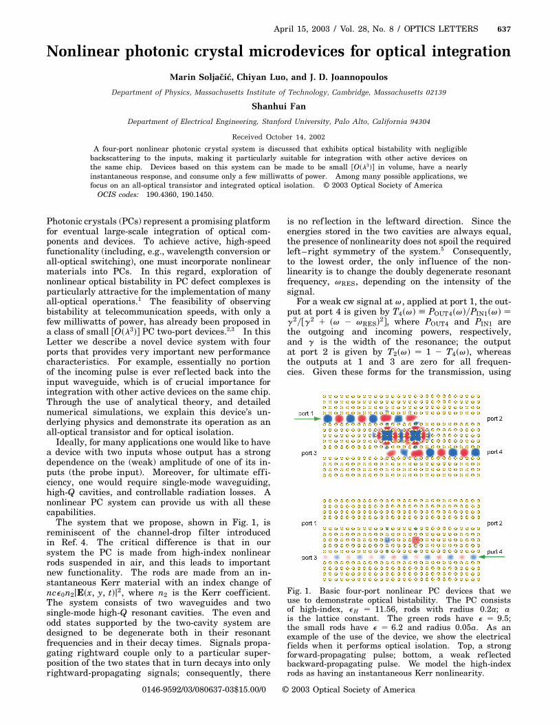
April 15, 2003 / Vol. 28, No. 8 / OPTICS LETTERS 637 Nonlinear photonic crystal microdevices for optical integration Marin Soljaˇ cic ´, Chiyan Luo, and J. D. Joannopoulos Department of Physics, Massachusetts Institute of Technology, Cambridge, Massachusetts 02139 Shanhui Fan Department of Electrical Engineering, Stanford University, Palo Alto, California 94304 Received October 14, 2002 A four-port nonlinear photonic crystal system is discussed that exhibits optical bistability with negligible backscattering to the inputs, making it particularly suitable for integration with other active devices on the same chip. Devices based on this system can be made to be small Ol 3 in volume, have a nearly instantaneous response, and consume only a few milliwatts of power. Among many possible applications, we focus on an all-optical transistor and integrated optical isolation. © 2003 Optical Society of America OCIS codes: 190.4360, 190.1450. Photonic crystals (PCs) represent a promising platform for eventual large-scale integration of optical com- ponents and devices. To achieve active, high-speed functionality (including, e.g., wavelength conversion or all-optical switching), one must incorporate nonlinear materials into PCs. In this regard, exploration of nonlinear optical bistability in PC defect complexes is particularly attractive for the implementation of many all-optical operations. 1 The feasibility of observing bistability at telecommunication speeds, with only a few milliwatts of power, has already been proposed in a class of small Ol 3 PC two-port devices. 2,3 In this Letter we describe a novel device system with four ports that provides very important new performance characteristics. For example, essentially no portion of the incoming pulse is ever reflected back into the input waveguide, which is of crucial importance for integration with other active devices on the same chip. Through the use of analytical theory, and detailed numerical simulations, we explain this device’s un- derlying physics and demonstrate its operation as an all-optical transistor and for optical isolation. Ideally, for many applications one would like to have a device with two inputs whose output has a strong dependence on the (weak) amplitude of one of its in- puts (the probe input). Moreover, for ultimate eff i- ciency, one would require single-mode waveguiding, high-Q cavities, and controllable radiation losses. A nonlinear PC system can provide us with all these capabilities. The system that we propose, shown in Fig. 1, is reminiscent of the channel-drop filter introduced in Ref. 4. The critical difference is that in our system the PC is made from high-index nonlinear rods suspended in air, and this leads to important new functionality. The rods are made from an in- stantaneous Kerr material with an index change of nce 0 n 2 jEx, y , tj 2 , where n 2 is the Kerr coefficient. The system consists of two waveguides and two single-mode high-Q resonant cavities. The even and odd states supported by the two-cavity system are designed to be degenerate both in their resonant frequencies and in their decay times. Signals propa- gating rightward couple only to a particular super- position of the two states that in turn decays into only rightward-propagating signals; consequently, there is no ref lection in the leftward direction. Since the energies stored in the two cavities are always equal, the presence of nonlinearity does not spoil the required left–right symmetry of the system. 5 Consequently, to the lowest order, the only influence of the non- linearity is to change the doubly degenerate resonant frequency, v RES , depending on the intensity of the signal. For a weak cw signal at v, applied at port 1, the out- put at port 4 is given by T 4 v P OUT 4 vP IN1 v g 2 g 2 1 v2v RES 2 , where P OUT 4 and P IN1 are the outgoing and incoming powers, respectively, and g is the width of the resonance; the output at port 2 is given by T 2 v 1 2 T 4 v, whereas the outputs at 1 and 3 are zero for all frequen- cies. Given these forms for the transmission, using Fig. 1. Basic four-port nonlinear PC devices that we use to demonstrate optical bistability. The PC consists of high-index, e H 11.56, rods with radius 0.2a; a is the lattice constant. The green rods have e 9.5; the small rods have e 6.2 and radius 0.05a. As an example of the use of the device, we show the electrical fields when it performs optical isolation. Top, a strong forward-propagating pulse; bottom, a weak ref lected backward-propagating pulse. We model the high-index rods as having an instantaneous Kerr nonlinearity. 0146-9592/03/080637-03$15.00/0 © 2003 Optical Society of America
Transcript of Nonlinear photonic crystal microdevices for optical ...soljacic/opt_trans_OL.pdf · displays...
April 15, 2003 / Vol. 28, No. 8 / OPTICS LETTERS 637
Nonlinear photonic crystal microdevices for optical integration
Marin Soljacic, Chiyan Luo, and J. D. Joannopoulos
Department of Physics, Massachusetts Institute of Technology, Cambridge, Massachusetts 02139
Shanhui Fan
Department of Electrical Engineering, Stanford University, Palo Alto, California 94304
Received October 14, 2002
A four-port nonlinear photonic crystal system is discussed that exhibits optical bistability with negligiblebackscattering to the inputs, making it particularly suitable for integration with other active devices onthe same chip. Devices based on this system can be made to be small �O�l3�� in volume, have a nearlyinstantaneous response, and consume only a few milliwatts of power. Among many possible applications, wefocus on an all-optical transistor and integrated optical isolation. © 2003 Optical Society of America
OCIS codes: 190.4360, 190.1450.
Photonic crystals (PCs) represent a promising platformfor eventual large-scale integration of optical com-ponents and devices. To achieve active, high-speedfunctionality (including, e.g., wavelength conversion orall-optical switching), one must incorporate nonlinearmaterials into PCs. In this regard, exploration ofnonlinear optical bistability in PC defect complexes isparticularly attractive for the implementation of manyall-optical operations.1 The feasibility of observingbistability at telecommunication speeds, with only afew milliwatts of power, has already been proposed ina class of small �O�l3�� PC two-port devices.2,3 In thisLetter we describe a novel device system with fourports that provides very important new performancecharacteristics. For example, essentially no portionof the incoming pulse is ever ref lected back into theinput waveguide, which is of crucial importance forintegration with other active devices on the same chip.Through the use of analytical theory, and detailednumerical simulations, we explain this device’s un-derlying physics and demonstrate its operation as anall-optical transistor and for optical isolation.
Ideally, for many applications one would like to havea device with two inputs whose output has a strongdependence on the (weak) amplitude of one of its in-puts (the probe input). Moreover, for ultimate eff i-ciency, one would require single-mode waveguiding,high-Q cavities, and controllable radiation losses. Anonlinear PC system can provide us with all thesecapabilities.
The system that we propose, shown in Fig. 1, isreminiscent of the channel-drop filter introducedin Ref. 4. The critical difference is that in oursystem the PC is made from high-index nonlinearrods suspended in air, and this leads to importantnew functionality. The rods are made from an in-stantaneous Kerr material with an index change ofnce0n2jE�x, y, t�j2, where n2 is the Kerr coeff icient.The system consists of two waveguides and twosingle-mode high-Q resonant cavities. The even andodd states supported by the two-cavity system aredesigned to be degenerate both in their resonantfrequencies and in their decay times. Signals propa-gating rightward couple only to a particular super-position of the two states that in turn decays into onlyrightward-propagating signals; consequently, there
0146-9592/03/080637-03$15.00/0
is no ref lection in the leftward direction. Since theenergies stored in the two cavities are always equal,the presence of nonlinearity does not spoil the requiredleft–right symmetry of the system.5 Consequently,to the lowest order, the only inf luence of the non-linearity is to change the doubly degenerate resonantfrequency, vRES, depending on the intensity of thesignal.
For a weak cw signal at v, applied at port 1, the out-put at port 4 is given by T4�v� � POUT4�v��PIN1�v� �g2��g2 1 �v 2 vRES�2�, where POUT4 and PIN1 arethe outgoing and incoming powers, respectively,and g is the width of the resonance; the outputat port 2 is given by T2�v� � 1 2 T4�v�, whereasthe outputs at 1 and 3 are zero for all frequen-cies. Given these forms for the transmission, using
Fig. 1. Basic four-port nonlinear PC devices that weuse to demonstrate optical bistability. The PC consistsof high-index, eH � 11.56, rods with radius 0.2a; ais the lattice constant. The green rods have e � 9.5;the small rods have e � 6.2 and radius 0.05a. As anexample of the use of the device, we show the electricalfields when it performs optical isolation. Top, a strongforward-propagating pulse; bottom, a weak ref lectedbackward-propagating pulse. We model the high-indexrods as having an instantaneous Kerr nonlinearity.
© 2003 Optical Society of America
638 OPTICS LETTERS / Vol. 28, No. 8 / April 15, 2003
perturbation theory with a small nonlinear indexchange, one can self-consistently f ind the nonlin-early induced resonance shift, and thereby thesteady-state transmission of cw signals through thesystem. Such analysis shows2 that the systemwill exhibit optical bistability if the carrier fre-quency v0 is sufficiently below the resonantfrequency, d � �vRES 2 v0��g .
p3, and that
the steady-state values of the cw powers arePOUT4
S�PIN1S � 1��1 1 �POUT4
S�P0 2 d�2�, andPOUT2
S�PIN1S � 1 2 POUT4
S�PIN1S , where characteris-
tic power P0 � 1��kQ2�vRES�c�n2�r�jMAX� and k is ameasure of nonlinear feedback given by
k �µ
cvRES
∂d
�
RVOL ddr�jE�r� ? E�r�j2 1 2jE�r� ? E��r�j2�n2�r�n2�r�
�RVOL ddrjE�r�j2n2�r��2n2�r�jMAX
,
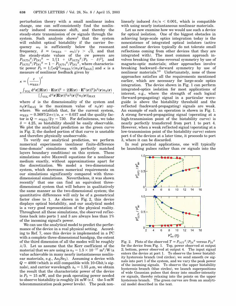
where d is the dimensionality of the system andn2�r�jMAX is the maximum value of n2�r� any-where. We establish that, for the current system,vRES � 0.3697�2pc��a, k � 0.037 and the quality fac-tor is Q � vRES�2g � 730. For definiteness, we taked � 4.25, so bistability should be easily observable.We plot the analytical prediction as the green curvein Fig. 2; the dashed portion of that curve is unstableand therefore physically unobservable.
To verify our analytical prediction, we performnumerical experiments (nonlinear finite-differencetime-domain6 simulations with perfectly matchedlayers boundary conditions) on this system. Thesesimulations solve Maxwell equations for a nonlinearmedium exactly, without approximations apart forthe discretization. We model a two-dimensionalsystem, which decreases numerical requirements onour simulations signif icantly compared with three-dimensional simulations. Nevertheless, it was shownrecently7 that one can find an equivalent three-dimensional system that will behave in qualitativelythe same manner as the two-dimensional system; thequantitative differences will only be of a geometricalfactor close to 1. As shown in Fig. 2, this devicedisplays optical bistability, and our analytical modelis a very good representation of the physical reality.Throughout all these simulations, the observed ref lec-tions back into ports 1 and 3 are always less than 1%of the incoming signal’s power.
We can use the analytical model to predict the perfor-mance of the device in a real physical setting. Accord-ing to Ref. 7, once this device is implemented in a PCwith a complete three-dimensional bandgap, the extentof the third dimension of all the modes will be roughlyl�3. Let us assume that the Kerr coeff icient of thematerial that we are using is n2 � 1.5 3 10217 m2�W (avalue achievable in many nearly instantaneous nonlin-ear materials, e.g., As2Se2). Assuming a device withQ � 4000 (which is still compatible with 10-Gbit�s sig-nals), and carrier wavelength l0 � 1.55 mm, we obtainthe result that the characteristic power of the deviceis P0 � 15 mW, and the peak operating power neededto observe bistability is roughly 24 mW (c.f. the 5-mWtelecommunication peak power levels). The peak non-
linearly induced dn�n , 0.001, which is compatiblewith using nearly instantaneous nonlinear materials.
Let us now examine how we would use such a devicefor optical isolation. One of the biggest obstacles inachieving large-scale optics integration today is thenonexistence of integrated optical isolators (activeand nonlinear devices typically do not tolerate smallref lections coming from other devices that they areintegrated with). The most common approach in-volves breaking the time-reversal symmetry by use ofmagneto-optic materials; other approaches involvebreaking backward–forward symmetry by use ofnonlinear materials.8,9 Unfortunately, none of theseapproaches satisfies all the requirements mentionedearlier, which are necessary for large-scale opticsintegration. The device shown in Fig. 1 can performintegrated-optics isolation for most applications ofinterest, e.g., where the strength of each logical(forward-propagating) signal in a particular wave-guide is above the bistability threshold and theref lected (backward-propagating) signals are weak.An example of such an operation is shown in Fig. 1.A strong forward-propagating signal (operating at ahigh-transmission point of the bistability curve) isnearly perfectly transferred from port 1 to port 4.However, when a weak ref lected signal (operating at alow-transmission point of the bistability curve) entersport 4 of the devices at a later time, it proceeds to port3, where it can be discarded.
In real practical applications, one will typicallybe launching pulses rather than cw signals into the
Fig. 2. Plots of the observed T � POUTS�PIN
S versus PINS
for the device from Fig. 1. Top, power observed at output2; bottom, power observed at output 4. The input signalenters the device at port 1. To observe the lower bistabil-ity hysteresis branch (red circles), we send smooth cw sig-nals into port 1 of the system, and we vary the peak powerof the incoming signals. To observe the upper bistabilityhysteresis branch (blue circles), we launch superpositionsof wide Gaussian pulses that decay into smaller-intensitycw signals, thereby relaxing into the points on the upperhysteresis branch. The green curves are from an analyti-cal model described in the text.
April 15, 2003 / Vol. 28, No. 8 / OPTICS LETTERS 639
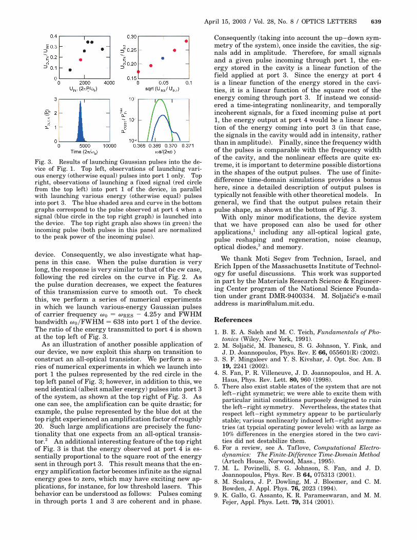
Fig. 3. Results of launching Gaussian pulses into the de-vice of Fig. 1. Top left, observations of launching vari-ous energy (otherwise equal) pulses into port 1 only. Topright, observations of launching a f ixed signal (red circlefrom the top left) into port 1 of the device, in parallelwith launching various energy (otherwise equal) pulsesinto port 3. The blue shaded area and curve in the bottomgraphs correspond to the pulse observed at port 4 when asignal (blue circle in the top right graph) is launched intothe device. The top right graph also shows (in green) theincoming pulse (both pulses in this panel are normalizedto the peak power of the incoming pulse).
device. Consequently, we also investigate what hap-pens in this case. When the pulse duration is verylong, the response is very similar to that of the cw case,following the red circles on the curve in Fig. 2. Asthe pulse duration decreases, we expect the featuresof this transmission curve to smooth out. To checkthis, we perform a series of numerical experimentsin which we launch various-energy Gaussian pulsesof carrier frequency v0 � vRES 2 4.25g and FWHMbandwidth v0�FWHM � 638 into port 1 of the device.The ratio of the energy transmitted to port 4 is shownat the top left of Fig. 3.
As an illustration of another possible application ofour device, we now exploit this sharp on transition toconstruct an all-optical transistor. We perform a se-ries of numerical experiments in which we launch intoport 1 the pulses represented by the red circle in thetop left panel of Fig. 3; however, in addition to this, wesend identical (albeit smaller energy) pulses into port 3of the system, as shown at the top right of Fig. 3. Asone can see, the amplif ication can be quite drastic; forexample, the pulse represented by the blue dot at thetop right experienced an amplification factor of roughly20. Such large amplifications are precisely the func-tionality that one expects from an all-optical transis-tor.2 An additional interesting feature of the top rightof Fig. 3 is that the energy observed at port 4 is es-sentially proportional to the square root of the energysent in through port 3. This result means that the en-ergy amplif ication factor becomes infinite as the signalenergy goes to zero, which may have exciting new ap-plications, for instance, for low threshold lasers. Thisbehavior can be understood as follows: Pulses comingin through ports 1 and 3 are coherent and in phase.
Consequently (taking into account the up–down sym-metry of the system), once inside the cavities, the sig-nals add in amplitude. Therefore, for small signalsand a given pulse incoming through port 1, the en-ergy stored in the cavity is a linear function of thefield applied at port 3. Since the energy at port 4is a linear function of the energy stored in the cavi-ties, it is a linear function of the square root of theenergy coming through port 3. If instead we consid-ered a time-integrating nonlinearity, and temporallyincoherent signals, for a f ixed incoming pulse at port1, the energy output at port 4 would be a linear func-tion of the energy coming into port 3 (in that case,the signals in the cavity would add in intensity, ratherthan in amplitude). Finally, since the frequency widthof the pulses is comparable with the frequency widthof the cavity, and the nonlinear effects are quite ex-treme, it is important to determine possible distortionsin the shapes of the output pulses. The use of finite-difference time-domain simulations provides a bonushere, since a detailed description of output pulses istypically not feasible with other theoretical models. Ingeneral, we find that the output pulses retain theirpulse shape, as shown at the bottom of Fig. 3.
With only minor modif ications, the device systemthat we have proposed can also be used for otherapplications,1 including any all-optical logical gate,pulse reshaping and regeneration, noise cleanup,optical diodes,3 and memory.
We thank Moti Segev from Technion, Israel, andErich Ippen of the Massachusetts Institute of Technol-ogy for useful discussions. This work was supportedin part by the Materials Research Science & Engineer-ing Center program of the National Science Founda-tion under grant DMR-9400334. M. Soljacic’s e-mailaddress is [email protected].
References
1. B. E. A. Saleh and M. C. Teich, Fundamentals of Pho-tonics (Wiley, New York, 1991).
2. M. Soljacic, M. Ibanescu, S. G. Johnson, Y. Fink, andJ. D. Joannopoulos, Phys. Rev. E 66, 055601(R) (2002).
3. S. F. Mingaleev and Y. S. Kivshar, J. Opt. Soc. Am. B19, 2241 (2002).
4. S. Fan, P. R. Villeneuve, J. D. Joannopoulos, and H. A.Haus, Phys. Rev. Lett. 80, 960 (1998).
5. There also exist stable states of the system that are notleft–right symmetric; we were able to excite them withparticular initial conditions purposely designed to ruinthe left–right symmetry. Nevertheless, the states thatrespect left–right symmetry appear to be particularlystable; various nonlinearly induced left–right asymme-tries (at typcial operating power levels) with as large as10% differences in the energies stored in the two cavi-ties did not destabilize them.
6. For a review, see A. Taf love, Computational Electro-dynamics: The Finite-Difference Time-Domain Method(Artech House, Norwood, Mass., 1995).
7. M. L. Povinelli, S. G. Johnson, S. Fan, and J. D.Joannopoulos, Phys. Rev. B 64, 075313 (2001).
8. M. Scalora, J. P. Dowling, M. J. Bloemer, and C. M.Bowden, J. Appl. Phys. 76, 2023 (1994).
9. K. Gallo, G. Assanto, K. R. Parameswaran, and M. M.Fejer, Appl. Phys. Lett. 79, 314 (2001).


![THERMAL BONDING OF POLYMER MICRODEVICES … · · 2013-02-27THERMAL BONDING OF POLYMER MICRODEVICES USING A PRESSURE -ASSISTED BOILING POINT CONTROL SYSTEM Taehyun Park 1, ... [Pa]](https://static.fdocuments.in/doc/165x107/5abf715d7f8b9aa15e8e0473/thermal-bonding-of-polymer-microdevices-bonding-of-polymer-microdevices-using.jpg)
![UNIVERSITÉ FRANÇOISRABELAIS DETOURS THÈSE · 1.28 Comparaisondes performancesde BGApar letest IPC-9702[18] . . . . . . 60 1.29 Méthode detest utiliséeparMotorola etAdvanced MicroDevices](https://static.fdocuments.in/doc/165x107/5f8a5091f039a82f860d2196/universit-franoisrabelais-detours-thse-128-comparaisondes-performancesde.jpg)


![INVITED PAPER PlasmonsinGraphene: …soljacic/graphene_Proceedings_IEEE.pdf · Polarization of graphene and plasmons under strain have been investigated in [54] and [55]. Plasmons](https://static.fdocuments.in/doc/165x107/5ae4b30d7f8b9ae1578b4a90/invited-paper-plasmonsingraphene-soljacicgrapheneproceedingsieeepdfpolarization.jpg)