
Nonlinear optics in photonic nanowires - … · Nonlinear optics in photonic nanowires Mark A....
21
Nonlinear optics in photonic nanowires Mark A. Foster 1 , Amy C. Turner 2 , Michal Lipson 2 , and Alexander L. Gaeta 1 1 School of Applied and Engineering Physics, Cornell University, Ithaca, NY 14853 2 School of Electrical and Computer Engineering, Cornell University, Ithaca, NY 14853 [email protected] Abstract: We review recent research on nonlinear optical interactions in waveguides with sub-micron transverse dimensions, which are termed photonic nanowires. Such nanowaveguides, fabricated from glasses or semiconductors, provide the maximal confinement of light for index guiding structures enabling large enhancement of nonlinear interactions and group-velocity dispersion engineering. The combination of these two properties make photonic nanowires ideally suited for many nonlinear optical applications including the generation of single-cycle pulses and optical processing with sub-mW powers. © 2008 Optical Society of America OCIS codes: (190.4370) Nonlinear optics, fibers; (190.4390) Nonlinear optics, integrated op- tics References and links 1. P. Dumais, F. Gonthier, S. Lacroix, A. Villeneuve, P. G. J. Wigley, and G. I. Stegeman, “Enhanced self-phase modulation in tapered fibers,” Opt. Lett. 18, 1996–1998 (1993). 2. D. Akimov, M. Schmitt, R. Maksimenka, K. Dukel’skii, Y. Kondrat’ev, A. Khokhlov, V. Shevandin, W. Kiefer, and A. M. Zheltikov, “Supercontinuum generation in a multiple-submicron-core microstructure fiber: toward limiting waveguide enhancement of nonlinear-optical processes,” Appl. Phys. B 77, 299–305 (2003). 3. A.M. Zheltikov, “The physical limit for the waveguide enhancement of nonlinear-optical processes,” Opt. Spec- trosc. 95, 410–415 (2003). 4. V. Finazzi, T. M. Monro, and D. J. Richardson, “The role of confinement loss in highly nonlinear silica holey fibers,” IEEE Photon. Technol. Lett. 15, 1246–1248 (2003). 5. M. A. Foster, K. D. Moll, A. L. Gaeta, “Optimal waveguide dimensions for nonlinear interactions,” Opt. Express 12, 2880–2887 (2004), http://www.opticsexpress.org/abstract.cfm?URI=OPEX-12-13-2880 . 6. Y. Lize, E. Magi, V. Ta’eed, J. Bolger, P. Steinvurzel, and B. Eggleton, “Microstructured opti- cal fiber photonic wires with subwavelength core diameter,” Opt. Express 12, 3209–3217 (2004), http://www.opticsinfobase.org/abstract.cfm?URI=oe-12-14-3209 . 7. C. Koos, L. Jacome, C. Poulton, J. Leuthold, and W. Freude, “Nonlinear silicon-on- insulator waveguides for all-optical signal processing,” Opt. Express 15, 5976–5990 (2007), http://www.opticsinfobase.org/abstract.cfm?URI=oe-15-10-5976 . 8. L. M. Tong, R. R. Gattass, J. B. Ashcom, S. L. He, J. Y. Lou, M. Y. Shen, I. Maxwell, and E. Mazur, “Subwavelength-diameter silica wires for low-loss optical wave guiding,” Nature 426, 816–819 (2003). 9. M. Hu, C. -y. Wang, Y. Li, Z. Wang, L. Chai, and A. Zheltikov, “Multiplex frequency conversion of unamplified 30-fs Ti: sapphire laser pulses by an array of waveguiding wires in a random-hole microstructure fiber,” Opt. Express 12, 6129–6134 (2004), http://www.opticsinfobase.org/abstract.cfm?URI=oe-12-25-6129 10. S. Leon-Saval, T. Birks, W. Wadsworth, P. St. J. Russell, M. Mason, “Supercontin- uum generation in submicron fibre waveguides,” Opt. Express 12, 2864–2869 (2004), http://www.opticsexpress.org/abstract.cfm?URI=OPEX-12-13-2864 . 11. N. A. Wolchover, F. Luan, A. K. George, J. C. Knight, and F. G. Omenetto, “High nonlinearity glass photonic crystal nanowires,” Opt. Express 15, 829–833 (2007), http://www.opticsinfobase.org/abstract.cfm?URI=oe-15-3-829 . 12. C. Grillet, C. Smith, D. Freeman, S. Madden, B. Luther-Davies, E. Magi, D. Moss, and B. Eggleton, “Efficient coupling to chalcogenide glass photonic crystal waveguides via silica optical fiber nanowires,” Opt. Express 14, 1070–1078 (2006), http://www.opticsinfobase.org/abstract.cfm?URI=oe-14-3-1070 . #89450 - $15.00 USD Received 6 Nov 2007; revised 5 Jan 2008; accepted 5 Jan 2008; published 16 Jan 2008 (C) 2008 OSA 21 January 2008 / Vol. 16, No. 2 / OPTICS EXPRESS 1300
-
Upload
nguyendiep -
Category
Documents
-
view
226 -
download
0
Transcript of Nonlinear optics in photonic nanowires - … · Nonlinear optics in photonic nanowires Mark A....
Nonlinear optics in photonic nanowires
Mark A. Foster1, Amy C. Turner2, Michal Lipson2, and Alexander L.Gaeta1
1School of Applied and Engineering Physics, Cornell University, Ithaca, NY 148532School of Electrical and Computer Engineering, Cornell University, Ithaca, NY 14853
Abstract: We review recent research on nonlinear optical interactionsin waveguides with sub-micron transverse dimensions, which are termedphotonic nanowires. Such nanowaveguides, fabricated from glasses orsemiconductors, provide the maximal confinement of light for indexguiding structures enabling large enhancement of nonlinear interactionsand group-velocity dispersion engineering. The combination of these twoproperties make photonic nanowires ideally suited for many nonlinearoptical applications including the generation of single-cycle pulses andoptical processing with sub-mW powers.
© 2008 Optical Society of AmericaOCIS codes: (190.4370) Nonlinear optics, fibers; (190.4390) Nonlinear optics, integrated op-tics
References and links1. P. Dumais, F. Gonthier, S. Lacroix, A. Villeneuve, P. G. J. Wigley, and G. I. Stegeman, “Enhanced self-phasemodulation in tapered fibers,” Opt. Lett. 18, 1996–1998 (1993).
2. D. Akimov, M. Schmitt, R. Maksimenka, K. Dukel’skii, Y. Kondrat’ev, A. Khokhlov, V. Shevandin, W. Kiefer,and A. M. Zheltikov, “Supercontinuum generation in a multiple-submicron-core microstructure fiber: towardlimiting waveguide enhancement of nonlinear-optical processes,” Appl. Phys. B 77, 299–305 (2003).
3. A. M. Zheltikov, “The physical limit for the waveguide enhancement of nonlinear-optical processes,” Opt. Spec-trosc. 95, 410–415 (2003).
4. V. Finazzi, T. M. Monro, and D. J. Richardson, “The role of confinement loss in highly nonlinear silica holeyfibers,” IEEE Photon. Technol. Lett. 15, 1246–1248 (2003).
5. M. A. Foster, K. D. Moll, A. L. Gaeta, “Optimal waveguide dimensions for nonlinear interactions,” Opt. Express12, 2880–2887 (2004), http://www.opticsexpress.org/abstract.cfm?URI=OPEX-12-13-2880.
6. Y. Lize, E. Magi, V. Ta’eed, J. Bolger, P. Steinvurzel, and B. Eggleton, “Microstructured opti-cal fiber photonic wires with subwavelength core diameter,” Opt. Express 12, 3209–3217 (2004),http://www.opticsinfobase.org/abstract.cfm?URI=oe-12-14-3209.
7. C. Koos, L. Jacome, C. Poulton, J. Leuthold, and W. Freude, “Nonlinear silicon-on-insulator waveguides for all-optical signal processing,” Opt. Express 15, 5976–5990 (2007),http://www.opticsinfobase.org/abstract.cfm?URI=oe-15-10-5976.
8. L. M. Tong, R. R. Gattass, J. B. Ashcom, S. L. He, J. Y. Lou, M. Y. Shen, I. Maxwell, and E. Mazur,“Subwavelength-diameter silica wires for low-loss optical wave guiding,” Nature 426, 816–819 (2003).
9. M. Hu, C. -y. Wang, Y. Li, Z. Wang, L. Chai, and A. Zheltikov, “Multiplex frequency conversion of unamplified30-fs Ti: sapphire laser pulses by an array of waveguiding wires in a random-hole microstructure fiber,” Opt.Express 12, 6129–6134 (2004), http://www.opticsinfobase.org/abstract.cfm?URI=oe-12-25-6129
10. S. Leon-Saval, T. Birks, W. Wadsworth, P. St. J. Russell, M. Mason, “Supercontin-uum generation in submicron fibre waveguides,” Opt. Express 12, 2864–2869 (2004),http://www.opticsexpress.org/abstract.cfm?URI=OPEX-12-13-2864.
11. N. A. Wolchover, F. Luan, A. K. George, J. C. Knight, and F. G. Omenetto, “Highnonlinearity glass photonic crystal nanowires,” Opt. Express 15, 829–833 (2007),http://www.opticsinfobase.org/abstract.cfm?URI=oe-15-3-829.
12. C. Grillet, C. Smith, D. Freeman, S. Madden, B. Luther-Davies, E. Magi, D. Moss, and B. Eggleton, “Efficientcoupling to chalcogenide glass photonic crystal waveguides via silica optical fiber nanowires,” Opt. Express 14,1070–1078 (2006), http://www.opticsinfobase.org/abstract.cfm?URI=oe-14-3-1070.
#89450 - $15.00 USD Received 6 Nov 2007; revised 5 Jan 2008; accepted 5 Jan 2008; published 16 Jan 2008(C) 2008 OSA 21 January 2008 / Vol. 16, No. 2 / OPTICS EXPRESS 1300

13. J. S. Foresi, P. R. Villeneuve, J. Ferrera, E. R. Thoen, G. Steinmeyer, S. Fan, J. D. Joannopoulos, L. C. Kimerling,H. I. Smith, and E. P. Ippen, “Photonic-bandgap microcavities in optical waveguides,” Nature 390, 143–145(1997).
14. Y. A. Vlasov and S. J. McNab, “Losses in single-mode silicon-on-insulator strip waveguides and bends,” Opt.Express 12, 1622–1631 (2004), http://www.opticsinfobase.org/abstract.cfm?URI=oe-12-8-1622.
15. J. P. Zhang, D. Y. Chu, S. L. Wu, S. T. Ho, W. G. Bi, C. W. Tu, R. C. Tiberio, “Photonic-wire laser,” Phys. Rev.Lett. 75, 2678–2681 (1995).
16. G. A. Siviloglou, S. Suntsov, R. El-Ganainy, R. Iwanow, G. I. Stegeman, D. N. Christodoulides, R.Morandotti, D. Modotto, A. Locatelli, C. De Angelis, F. Pozzi, C. R. Stanley, and M. Sorel, “En-hanced third-order nonlinear effects in optical AlGaAs nanowires,” Opt. Express 14, 9377–9384 (2006),http://www.opticsinfobase.org/abstract.cfm?URI=oe-14-20-9377.
17. L. Tong, J. Lou, and E. Mazur, “Single-mode guiding properties of subwavelength-diameter silica and silicon wire waveguides,” Opt. Express 12, 1025–1035 (2004),http://www.opticsinfobase.org/abstract.cfm?URI=oe-12-6-1025.
18. L. Yin, Q. Lin, G. P. Agrawal, “Dispersion tailoring and soliton propagation in silicon waveguides,” Opt. Lett.31, 1295–1297 (2006).
19. E. Dulkeith, F. Xia, L. Schares, W. M. J. Green, Y. A. Vlasov, “Group index and groupvelocity dispersion in silicon-on-insulator photonic wires,” Opt. Express. 14, 3853–3863 (2006),http://www.opticsinfobase.org/abstract.cfm?URI=oe-14-9-3853 .
20. A. C. Turner, C. Manolatou, B. S. Schmidt, M. Lipson, M. A. Foster, J. E. Sharping, A. L. Gaeta, “Tai-lored anomalous group-velocity dispersion in silicon channel waveguides,” Opt. Express 14, 4357–4362 (2006),http://www.opticsinfobase.org/abstract.cfm?URI=oe-14-10-4357.
21. V. R. Almeida, C. A. Barrios, R. R. Panepucci, M. Lipson, M. A. Foster, D. G. Ouzounov, and A. L. Gaeta,“All-optical switching on a silicon chip,” Opt. Lett. 29, 2867–2869 (2004).
22. R. Espinola, J. Dadap, R. Osgood, Jr., S. McNab, and Y. Vlasov, “Raman amplificationin ultrasmall silicon-on-insulator wire waveguides,” Opt. Express 12, 3713–3718 (2004),http://www.opticsinfobase.org/abstract.cfm?URI=oe-12-16-3713.
23. D. Dimitropoulos, R. Jhaveri, R. Claps, J. C. S. Woo, and B. Jalali, “Lifetime of photogenerated carriers insilicon-on-insulator rib wavegudies,” Appl. Phys. Lett. 86 071115 (2005).
24. A. Zheltikov, “Gaussian-mode analysis of waveguide-enhanced Kerr-type nonlinearity of optical fibers and pho-tonic wires,” J. Opt. Soc. Am. B 22 1100–1104 (2005).
25. G. P. Agrawal, Nonlinear Fiber Optics (Academic Press, Boston, 1989).26. A. W. Snyder and J. D. Love, Optical Waveguide Theory (Kluwer Academic Publishers, 1983).27. C. R. Pollock and M. Lipson, Integrated Photonics (Kluwer Academic Publishers, 2003).28. J. K. Ranka, R. S. Windeler, and A. J. Stentz, “Visible continuum generation in air silica microstructure optical
fibers with anomalous dispersion at 800nm,” Opt. Lett. 25, 25–27 (2000).29. W. J. Wadsworth, A. Ortigosa-Blanch, J. C. Knight, T. A. Birks, T. -P. M. Man, and P. S. J. Russell, “Supercon-
tinuum generation in photonic crystal fibers and optical fiber tapers: a novel light source,” J. Opt. Soc. Am. B 19,2148–2155 (2002).
30. A. V. Husakou and J. Herrmann, “Supercontinuum generation of higher-order solitons by fission in photoniccrystal fibers,” Phys. Rev. Lett. 87, 203901 (2001).
31. A. L. Gaeta, “Nonlinear propagation and continuum generation in microstructured optical fibers,” Opt. Lett. 27,924–926 (2002).
32. J. M. Dudley and S. Coen, “Numerical simulations and coherence properties of supercontinuum generation inphotonic crystal and tapered optical fibers,” IEEE J. Sel. Top. Quantum Electron. 8, 651–659 (2002).
33. J. M. Dudley, L. Provino, N. Grossard, H. Maillotte, R. S. Windeler, B. J. Eggleton, and S. Coen, “Supercon-tinuum generation in air-silica microstrcutured fibers with nanosecond and femtosecond pulse pumping,” J. Opt.Soc. Am. B 19, 765–771 (2002).
34. J. M. Dudley, G. Genty, and S. Coen, “Supercontinuum generation in photonic crystal fiber,” Rev. Mod. Phys.78, 1135–1184 (2006).
35. T. A. Birks and Y. W. Li, “The shape of fiber tapers,” J. Lightwave Technol. 10, 432–438 (1992).36. L. Shi, X. Chen, H. Liu, Y. Chen, Z. Ye, W. Liao, and Y. Xia, “Fabrication of submicron-
diameter silica fibers using electric strip heater,” Opt. Express 14, 5055–5060 (2006),http://www.opticsinfobase.org/abstract.cfm?URI=oe-14-12-5055.
37. R. R. Gattass, G. T. Svacha, L. Tong, and E. Mazur, “Supercontinuum genera-tion in submicrometer diameter silica fibers,” Opt. Express 14, 9408–9414 (2006),http://www.opticsinfobase.org/abstract.cfm?URI=oe-14-20-9408.
38. E. Magi, P. Steinvurzel, and B. Eggleton, “Tapered photonic crystal fibers,” Opt. Express 12, 776–784 (2004),http://www.opticsinfobase.org/abstract.cfm?URI=oe-12-5-776.
39. M. A. Foster and A. L. Gaeta, “Ultra-low threshold supercontinuum generation in sub-wavelength waveguides,”Opt. Express 12, 3137–3143 (2004), http://www.opticsinfobase.org/abstract.cfm?URI=oe-12-14-3137.
40. L. Tong, L. Hu, J. Zhang, J. Qiu, Q. Yang, J. Lou, Y. Shen, J. He, and Z. Ye, “Pho-
#89450 - $15.00 USD Received 6 Nov 2007; revised 5 Jan 2008; accepted 5 Jan 2008; published 16 Jan 2008(C) 2008 OSA 21 January 2008 / Vol. 16, No. 2 / OPTICS EXPRESS 1301

tonic nanowires directly drawn from bulk glasses,” Opt. Express 14, 82–87 (2006),http://www.opticsinfobase.org/abstract.cfm?URI=oe-14-1-82.
41. E. Magi, H. Nguyen, and B. Eggleton, “Air-hole collapse and mode transitions in microstructured fiber photonicwires,” Opt. Express 13, 453–459 (2005), http://www.opticsinfobase.org/abstract.cfm?URI=oe-13-2-453.
42. M. Kolesik and J. V. Moloney, “Nonlinear optical pulse propagation simulation: From Maxwell’s to unidirec-tional equations,” Phys. Rev. E 70, 036604 (2004).
43. M. Kolesik, E. M. Wright, and J. V. Moloney, “Simulation of femtosecond pulse propagation in sub-microndiameter tapered fibers,” Appl. Phys. B 79, 293–300 (2004).
44. B. Kibler, J. M. Dudley, and S. Coen, “Supercontinuum generation and nonlinear pulse propagation in photoniccrystal fiber: influence of the frequency-dependent effective area,” Appl. Phys. B 81, 337–342 (2005).
45. M. A. Foster, J. M. Dudley, B. Kibler, Q. Cao, D. Lee, R. Trebino, and A. L. Gaeta, “Nonlinear pulse propagationand supercontinuum generation in photonic nanowires: experiment and simulation,” Appl. Phys. B 81, 363–367(2005).
46. B. T. Kuhlmey, H. C. Nguyen, M. J. Steel, and B. J. Eggleton, “Confinement loss in adiabatic photonic crystalfiber tapers,” J. Opt. Soc. Am. B 23, 1965–1974 (2006).
47. C. M. B. Cordeiro, W. J. Wadsworth, T. A. Birks, and P. S. J. Russell, “Engineering the dispersion of taperedfibers for supercontinuum generation with a 1064 nm pump laser,” Opt. Lett. 30, 1980–1982 (2005).
48. J. C. Travers, S. V. Popov, and J. R. Taylor, “Extended blue supercontinuum generation in cascaded holey fibers,”Opt. Lett. 30, 3132–3134 (2005).
49. C. Xiong, A. Witkowska, S. G. Leon-Saval, T. A. Birks, and W. J. Wadsworth, “Enhanced vis-ible continuum generation from a microchip 1064nm laser,” Opt. Express 14, 6188–6193 (2006),http://www.opticsinfobase.org/abstract.cfm?URI=oe-14-13-6188.
50. M. A. Foster, A. L. Gaeta, Q. Cao, and R. Trebino, “Soliton-effect compression of supercon-tinuum to few-cycle durations in photonic nanowires,” Opt. Express 13, 6848–6855 (2005),http://www.opticsinfobase.org/abstract.cfm?URI=oe-13-18-6848.
51. M. A. Foster, Q. Cao, R. Trebino, and A. L. Gaeta, “Pulse Self-Compression of Supercontinuum in PhotonicNanowires,” in 15th International Conference on Ultrafast Phenomena, OSA Technical Digest Series (CD) (Op-tical Society of America, 2006), paper WC5.
52. M. V. Tognetti and H. M. Crespo, “Sub-two-cycle soliton-effect pulse compression at 800 nm in photonic crystalfibers,” J. Opt. Soc. Am. B 24, 1410–1415 (2007).
53. N. Akhmediev and M. Karlsson, “Cherenkov radiation emitted by solitons in optical fibers,” Phys. Rev. A 51,2602–2607 (1995).
54. I. Cristiani, R. Tediosi, L. Tartara, and V. Degiorgio, “Dispersive wave generation by solitons in microstructuredoptical fibers,” Opt. Express 12, 124–135 (2004), http://www.opticsinfobase.org/abstract.cfm?URI=oe-12-1-124.
55. A. B. Fedotov, S. O. Konorov, E. E. Serebryannikov, D. A. Sidorov-Biryukov, V. P. Mitrokhin, K, V, Dukel’skii,A. V. Khokhlov, V. S. Shevandin, Yu. N. Kondrat’ev, M. Scalora, and A. M. Zheltikov, “Assorted non-linearoptics in microchannel waveguides of photonic-crystal fibers,” Opt. Commun. 255, 218–224 (2005).
56. S. O. Konorov, D. A. Akimov, E. E. Serebryannikov, A. A. Ivanov, M. V. Alfimov, K. V. Dukel’skii, A. V.Khokhlov, V. S. Shevandin, Yu. N. Kondrat’ev, and A. M. Zheltikov, “High-order modes of photonic wiresexcited by the Cherenkov emission of solitons,” Laser Phys. Lett. 2, 258–261 (2005).
57. D. Akimov, T. Siebert, W. Kiefer, and A. Zheltikov, “Optical parametric amplification of a blueshifted output ofa photonic-crystal fiber,” J. Opt. Soc. Am. B 23, 1988–1993 (2006).
58. H. K. Tsang, C. S. Wong, T. K. Liang, I. E. Day, S. W. Roberts, A. Harpin, J. Drake, M. Asghari, “Opticaldispersion, two-photon absorption and self-phase modulation in silicon waveguides at 1.5 µmwavelength,” Appl.Phys. Lett. 80, 416–418 (2002).
59. M. Dinu, F. Quochi, H. Garcia, “Third-order nonlinearities in silicon at telecom waveguides,” Appl. Phys. Lett.82, 2954–2956 (2003).
60. D. J. Moss, L. Fu, I. Littler, B. J. Eggleton, “Ultrafast all-optical modulation via two-photon absorption in silicon-on-insulator waveguides,” Electron. Lett. 41, 320–321 (2005).
61. T. Liang, L. Nunes, T. Sakamoto, K. Sasagawa, T. Kawanishi, M. Tsuchiya, G. Priem, D.Van Thourhout, P. Dumon, R. Baets, H. Tsang, “Ultrafast all-optical switching by cross-absorption modulation in silicon wire waveguides,” Opt. Express 13, 7298–7303 (2005),http://www.opticsinfobase.org/abstract.cfm?URI=oe-13-19-7298.
62. T. K. Liang, L. R. Nunes, M. Tsuchiya, K. S. Abedin, T. Miyazaki, D. Van Thourhout, W. Bogaerts, P. Dumon, R.Baets, H. K. Tsang, “High speed logic gate using two-photon absoprtion in silicon waveguides,” Opt. Commun.265 171–174 (2006).
63. R. A. Soref, B. R. Bennett, “Electrooptical effects in silicon,” IEEE J. Quantum Electron. 23, 123–129 (1987).64. S. Stepanov, S. Ruschin, “Modulation of light by light in silicon-on-insulator waveguides,” Appl. Phys. Lett. 83,
5151–5153 (2003).65. V. R. Almeida, C. A. Barrios, R. R. Panepucci, M. Lipson, “All-optical control of light on a silicon chip,” Nature
431, 1081–1084 (2004).66. V. R. Almeida, Q. Xu, M. Lipson, “Ultrafast integrated semiconductor optical modulator based on the plasma-
#89450 - $15.00 USD Received 6 Nov 2007; revised 5 Jan 2008; accepted 5 Jan 2008; published 16 Jan 2008(C) 2008 OSA 21 January 2008 / Vol. 16, No. 2 / OPTICS EXPRESS 1302

dispersion effect,” Opt. Lett. 30 2403–2405 (2005).67. S. F. Preble, Q. Xu, B. S. Schmidt, M. Lipson, “Ultrafast all-optical modulation on a silicon chip,” Opt. Lett. 30
2891–2893 (2005).68. Q. Xu, M. Lipson, “Carrier-induced optical bistability in silicon ring resonators,” Opt. Lett. 31 341–343 (2006).69. C. Manolatou, M. Lipson, “All-optical silicon modulators based on carrier injection by two-photon absorption,”
J. Lightwave Technol. 24 1433–1439 (2006).70. Q. Xu, M. Lipson, “All-optical logic based on silicon micro-ring resonators,” Opt. Express 15 924–929 (2007),
http://www.opticsinfobase.org/abstract.cfm?URI=oe-15-3-924.71. S. F. Preble, Q. Xu, M. Lipson, “Changing the colour of light in a silicon resonator,” Nature Photonics 1 293–296
(2007).72. P. Dong, S. F. Preble, M. Lipson, “All-optical compact silicon comb switch,” Opt. Express 15 9600–9605 (2007),
http://www.opticsinfobase.org/abstract.cfm?URI=oe-15-15-9600.73. R. Claps, D. Dimitropoulos, Y. Han, B. Jalali, “Observation of Raman emission in silicon waveguides at 1.54 m,”
Opt. Express 10, 1305–1313 (2002), http://www.opticsexpress.org/abstract.cfm?URI=OPEX-10-22-1305.74. R. Claps, D. Dimitropoulos, B. Jalali, “Stimulated Raman scattering in silicon waveguides,” IEEE Electron. Lett.
38, 1352–1354 (2002).75. R. Claps, D. Dimitropoulos, V. Raghunathan, Y. Han, B. Jalali, “Observation of stimu-
lated Raman amplification in silicon waveguides,” Opt. Express 11, 1731–1739 (2003),http://www.opticsinfobase.org/abstract.cfm?URI=oe-11-15-1731.
76. T. K. Liang, H. K. Tsang, “Role of free carriers from two-photon absorption in Raman amplification in silicon-on-insulator waveguides,” Appl. Phys. Lett. 84, 2745–2747 (2004).
77. R. Claps, V. Raghunathan, D. Dimitropoulos, B. Jalali, “Influence of nonlinear absorp-tion on Raman amplification in Silicon waveguides,” Opt. Express 12, 2774–2780 (2004),http://www.opticsexpress.org/abstract.cfm?URI=OPEX-12-12-2774.
78. Q. Xu, V. Almeida, M. Lipson, “Time-resolved study of Raman gain in highlyconfined silicon-on-insulator waveguides,” Opt. Express 12, 4437–4442 (2004),http://www.opticsinfobase.org/abstract.cfm?URI=oe-12-19-4437.
79. O. Boyraz, B. Jalali, “Demonstration of a silicon Raman laser,” Opt. Express 12, 5269–5273 (2004),http://www.opticsinfobase.org/abstract.cfm?URI=oe-12-21-5269.
80. J. I. Dadap, R. L. Espinola, R. M. Osgood Jr., S. J. McNab, Y. A. Vlasov, “Spontaneous Raman scattering inultrasmall silicon waveguides,” Opt. Lett. 29, 2755–2757 (2004).
81. Q. Xu, V. R. Almeida, M. Lipson, “Demonstration of high Raman gain in a submicrometer-size silicon-on-insulator waveguide,” Opt. Lett. 30, 35–37 (2005).
82. V. Raghunathan, R. Claps, D. Dimitropoulos, B. Jalali, “Parametric Raman Wavelength Conversion in ScaledSilicon Waveguides,” J. Lightwave Technol. 23, 2094–2102 (2005).
83. R. Jones, H. Rong, A. Liu, A. Fang, M. Paniccia, D. Hak, O. Cohen, “Net continuous wave optical gain ina low loss silicon-on-insulator waveguide by stimulated Raman scattering,” Opt. Express 13, 519–525 (2005),http://www.opticsinfobase.org/abstract.cfm?URI=oe-13-2-519.
84. H. Rong, A. Liu, R. Jones, O. Cohen, D. Hak, R. Nicolaescu, A. Fang, M. Panniccia, “An all-silicon Ramanlaser,” Nature 433, 292–294 (2005).
85. H. Rong, R. Jones, A. Liu, O. Cohen, D. Hak, A. Fang, M. Paniccia, “A continuous-wave Raman silicon laser,”Nature 433, 725–728 (2005).
86. S. Blair, K. Zheng, “Intensity-tunable group delay using stimulated Raman scat-tering in silicon slow-light waveguides,” Opt. Express 14, 1064–1069 (2006),http://www.opticsinfobase.org/abstract.cfm?URI=oe-14-3-1064.
87. Y. Okawachi, M. A. Foster, J. E. Sharping, A. L. Gaeta, Q. Xu, M. Lipson, “All-optical slow-light on a photonicchip,” Opt. Express 14, 2317–2322 (2006), http://www.opticsinfobase.org/abstract.cfm?URI=oe-14-6-2317.
88. D. Dimitropoulos, V. Raghunathan, R. Claps, B. Jalali, “Phase-matching and non-linear optical processes in silicon waveguides,” Opt. Express 12, 149–160 (2004),http://www.opticsinfobase.org/abstract.cfm?URI=oe-12-1-149.
89. O. Boyraz, T. Indukuri, B. Jalali, “Self-phase-modulation induced spectral broadening in silicon waveguides,”Opt. Express 12, 829–834 (2004), http://www.opticsinfobase.org/abstract.cfm?URI=oe-12-5-829.
90. A. Cowan, G. Rieger, J. Young, “Nonlinear transmission of 1.5 µm pulses through single-mode silicon-on-insulator waveguide structures,” Opt. Express 12, 1611–1621 (2004),http://www.opticsinfobase.org/abstract.cfm?URI=oe-12-8-1611.
91. O. Boyraz, P. Koonath, V. Raghunathan, B. Jalali, “All optical switching and con-tinuum generation in silicon waveguides,” Opt. Express 12, 4094–4102 (2004),http://www.opticsinfobase.org/abstract.cfm?URI=oe-12-17-4094.
92. R. L. Espinola, J. I. Dadap, R. M. Osgood, S. J. McNab, Y. A. Vlasov, “C-band wave-length conversion in silicon photonic wire waveguides,” Opt. Express 13, 4341–4349 (2005),http://www.opticsinfobase.org/abstract.cfm?URI=oe-13-11-4341.
93. H. Fukuda, K. Yamada, T. Shoji, M. Takahashi, T. Tsuchizawa, T. Watanabe, J. Takahashi, S.
#89450 - $15.00 USD Received 6 Nov 2007; revised 5 Jan 2008; accepted 5 Jan 2008; published 16 Jan 2008(C) 2008 OSA 21 January 2008 / Vol. 16, No. 2 / OPTICS EXPRESS 1303

Itabashi, “Four-wave mixing in silicon wire waveguides,” Opt. Express 13, 4629–4637 (2005),http://www.opticsinfobase.org/abstract.cfm?URI=oe-13-12-4629.
94. H. Rong, Y. -H. Kuo, A. Liu, M. Paniccia, O. Cohen, “High efficiency wavelength con-version of 10 Gb/s data in silicon waveguides,” Opt. Express 14, 1182–1188 (2006),http://www.opticsinfobase.org/abstract.cfm?URI=oe-14-3-1182.
95. M. A. Foster, A. C. Turner, J. E. Sharping, B. S. Schmidt, M. Lipson, A. L. Gaeta, “Broad-band optical parametricgain on a silicon photonic chip,” Nature 441, 960–963 (2006).
96. K. Yamada, H. Fukuda, T. Tsuchizawa, T. Watanabe, T. Shoji, S. Itabashi, “All-optical efficient wavelengthconversion using silicon photonic wire waveguide,” IEEE Photon. Technol. Lett. 18, 1046–1048 (2006).
97. Q. Lin, J. Zhang, P. M. Fauchet, G. P. Agrawal, “Ultrabroadband parametric generationand wavelength conversion in silicon waveguides,” Opt. Express 14, 4786–4799 (2006),http://www.opticsinfobase.org/abstract.cfm?URI=oe-14-11-4786.
98. E. Dulkeith, Y. A. Vlasov, X. Chen, N. C. Panoiu, R. M. Osgood, Jr., “Self-phase-modulationin submicron silicon-on-insulator photonic wires,” Opt. Express 14, 5524–5534 (2006),http://www.opticsinfobase.org/abstract.cfm?URI=oe-14-12-5524.
99. R. Dekker, A. Driessen, T. Wahlbrink, C. Moormann, J. Niehusmann, M. Forst, “Ultrafast Kerr-induced all-optical wavelength conversion in silicon waveguides using 1.55 µm femtosecond pulses,” Opt. Express 14, 8336–8346 (2006), http://www.opticsinfobase.org/abstract.cfm?URI=oe-14-18-8336.
100. Y. -H. Kuo, H. Rong, V. Sih, S. Xu, M. Paniccia, O. Cohen, “Demonstration of wavelengthconversion at 40 Gb/s data rate in silicon waveguides,” Opt. Express 14, 11721–11726 (2006),http://www.opticsinfobase.org/abstract.cfm?URI=oe-14-24-11721.
101. I. W. Hsieh, X. Chen, J. I. Dadap, N. C. Panoiu, R. M. Osgood, S. J. McNab, Y. A. Vlasov, “Ultrafast-pulse self-phase modulation and third-order dispersion in Si photonic wire-waveguides,” Opt. Express 14, 12380–12387(2006), http://www.opticsinfobase.org/abstract.cfm?URI=oe-14-25-12380.
102. J. E. Sharping, K. F. Lee, M. A. Foster, A. C. Turner, B. S. Schmidt, M. Lipson, A. L. Gaeta, P. Kumar,“Generation of correlated photons in nanoscale silicon waveguides,” Opt. Express 14, 12388–12393 (2006),http://www.opticsinfobase.org/abstract.cfm?URI=oe-14-25-12388.
103. L. Yin, Q. Lin, G. P. Agrawal, “Soliton fission and supercontinuum generation in silicon waveguides,” Opt. Lett.32, 391–393 (2007).
104. I. W. Hsieh, X. Chen, J. I. Dadap, N. C. Panoiu, R. M. Osgood, Jr., S. J. McNab, Y. A. Vlasov, “Cross-phasemodulation-induced spectral and temporal effects on co-propagating femtosecond pulses in silicon photonicwires,” Opt. Express 15, 1135–1146 (2007), http://www.opticsinfobase.org/abstract.cfm?URI=oe-15-3-1135.
105. J. Zhang, Q. Lin, G. Piredda, R. W. Boyd, G. P. Agrawal, P. M. Fauchet, “Optical solitons in a silicon waveguide,”Opt. Express 15, 7682–7688 (2007), http://www.opticsinfobase.org/abstract.cfm?URI=oe-15-12-7682.
106. R. Salem, M. A. Foster, A. C. Turner, D. F. Geraghty, M. Lipson, A. L. Gaeta,“All-optical regeneration on a silicon chip,” Opt. Express 15, 7802–7809 (2007),http://www.opticsinfobase.org/abstract.cfm?URI=oe-15-12-7802.
107. M. A. Foster, A. C. Turner, R. Salem, M. Lipson, A. L. Gaeta, “Broad-band continuous-waveparametric wavelength conversion in silicon nanowaveguides,” Opt. Express 15, 12949–12958 (2007),http://www.opticsinfobase.org/abstract.cfm?URI=oe-15-20-12949.
108. R. Salem, M. A. Foster, A. C. Turner, D. F. Geraghty, M. Lipson, A. L. Gaeta, “Signal regeneration using low-power four-wave mixing on silicon chip,” Nature Photonics 2, 35–38 (2008).
109. A. C. Turner, M. A. Foster, A. L. Gaeta, and M. Lipson, “Ultra-low power nonlinear frequency conversion in asilicon photonic structure,” submitted for publication.
110. I.W. Hsieh, X. G. Chen, X. P. Liu, J. I. Dadap, N. C. Panoiu, C. Y. Chou, F. N. Xia, W.M. Green, Y. A. Vlasov, andR. M. Osgood, “Supercontinuum generation in silicon photonic wires,” Opt. Express 15, 15242–15249 (2007).
111. A. D. Bristow, N, Rotenberg, H. M. van Driel, “Two-photon absorption and Kerr coefficiecnts of silicon for850-2200 nm,” Appl. Phys. Lett. 90, 191104 (2007).
112. Q. Lin, J. Zhang, G. Piredda, R. W. Boyd, P. M. Fauchet, G. P. Agrawal, “Dispersion of silicon nonlinearities inthe near infrared region,” Appl. Phys. Lett. 91, 021111 (2007).
113. A. Chin, K. Y. Lee, B. C. Lin, S. Horng, “Picosecond photoresponse of carriers in Si ion-implanted Si,” Appl.Phys. Lett. 69, 653–655 (1996).
114. P. V. Mamyshev, “All-optical data regeneration based on self-phase modulation effect,” in Proc. European Con-ference on Optical Communications (ECOC98), p. 475, (1998).
115. K. P. Nayak, P. N. Melentiev, M. Morinaga, F. L. Kien, V. I. Balykin, K. Hakuta, “Optical nanofiber asan efficient tool for manipulating and probing atomic fluorescence,” Opt. Express 15, 5431–5438 (2007),http://www.opticsinfobase.org/abstract.cfm?URI=oe-15-9-5431.
116. E. C. Magi, L. B. Fu, H. C. Nguyen, M. R. Lamont, D. I. Yeom, B. J. Eggleton, “Enhanced Kerr nonlin-earity in sub-wavelength diameter As2Se3 chalcogenide fiber tapers,” Opt. Express 15, 10324–10329 (2007),http://www.opticsinfobase.org/abstract.cfm?URI=oe-15-16-10324.
117. M. R. Lamont, C. M. de Sterke, and B. J. Eggleton, “Dispersion engineering of highly nonlinearAs2S3 waveguides for parametric gain and wavelength conversion,” Opt. Express 15, 9458–9463 (2007),
#89450 - $15.00 USD Received 6 Nov 2007; revised 5 Jan 2008; accepted 5 Jan 2008; published 16 Jan 2008(C) 2008 OSA 21 January 2008 / Vol. 16, No. 2 / OPTICS EXPRESS 1304

http://www.opticsinfobase.org/abstract.cfm?URI=oe-15-15-9458.118. P. P. Absil, J. V. Hryniewicz, B. E. Little, P. S. Cho, R. A. Wilson, L. G. Joneckis, P. T. Ho, “Wavelength
conversion in GaAs micro-ring resonators,” Opt. Lett. 25, 554–556 (2000).119. V. Van, T. A. Ibrahim, P. P. Absil, F. G. Johnson, R. Grover, P. T. Ho, “Optical signal processing using nonlinear
semiconductor microring resonators,” IEEE J. Sel. Tops. Quantum Electron. 8, 705–713 (2002).120. J. E. Heebner, N. N. Lepeshkin, A. Schweinsberg, G. W. Wicks, R. W. Boyd, R. Grover, P. T. Ho, “Enhanced
linear and nonlinear optical phase response of AlGaAs microring resonators,” Opt. Lett. 29, 769–771 (2004).121. R. El-Ganainy, S. Mokhov, K. G. Makris, D. N. Christodoulides, R. Morandotti, “Soli-
tons in dispersion-inverted AlGaAs nanowires,” Opt. Express 14, 2277–2282 (2006),http://www.opticsinfobase.org/abstract.cfm?URI=oe-14-6-2277.
122. J. Meier, W. S. Mohammed, A. Jugessur, L. Qian, M. Mojahedi, J. S. Aitchison,“Group velocity inversion in AlGaAs nanowires,” Opt. Express 15, 12755–12762 (2007),http://www.opticsinfobase.org/abstract.cfm?URI=oe-15-20-12755.
123. F. Benabid, J. C. Knight, G. Antonopoulos, and P. St. J. Russell, “Stimulated Raman scattering in hydrogen-filledhollow-core photonic crystal fiber,” Science 298, 399–402 (2002).
124. D. G. Ouzounov, F. R. Ahmad, D. Muller, N. Venkataraman, M. T. Gallagher, M. G. Thomas, J. Silcox, K.W. Koch, and A. L. Gaeta, “Generation of megawatt optical solitons in hollow-core photonic band-gap fibers,”Science 301, 1702–1704 (2003).
125. F. Benabid, G. Bouwmans, J. C. Knight, and P. St. J. Russell, “Ultrahigh efficiency laser wavelength conversionin a gas-filled hollow core photonic crystal fiber by pure stimulated Raman scattering in molecular hydrogen,”Phys. Rev. Lett. 93, 123903 (2004).
126. S. Ghosh, J. E. Sharping, D. G. Ouzounov, and A. L. Gaeta, “Resonant optical interactions with moleculesconfined in photonic band-gap fibers,” Phys. Rev. Lett. 94, 093902 (2005).
127. S. Ghosh, A. R. Bhagwat, C. K. Renshaw, S. Goh, A. L. Gaeta, and B. J. Kirby, “Low-light-level optical interac-tions with rubidium vapor in a photonic band-gap fiber,” Phys. Rev. Lett. 97, 023603 (2006).
128. V. R. Almeida, Q. Xu, C. A. Barrios, M. Lipson, “Guiding and confining light in void nanostructure,” Opt. Lett.29, 1209–1211 (2004).
129. J. T. Robinson, C. Manolatou, L. Chen, M. Lipson, “Ultrasmall mode volumes in dielectric optical microcavities,”Phys. Rev. Lett. 95, 143901 (2005).
130. G. S. Wiederhecker, C. M. B. Cordeiro, F. Couny, F. Benabid, S. A. Maier, J. C. Knight, C. H. B. Cruz, H.L. Fragnito, “Field enhancement within an optical fibre with a subwavelength air core,” Nature Photonics 1,115–118 (2007).
1. Introduction
Nonlinear optical processes benefit from high optical intensities and long interaction lengths. Ina bulk geometry, achieving higher intensities from a fixed optical power requires tighter focus-ing. However, such focusing leads to a shortened interaction length due to the reduced confocalparameter, which for many nonlinear processes results in no net increase in efficiency despitethe higher intensities. Waveguiding geometries, such as optical fibers enable high optical inten-sities over extended interaction lengths as long as km’s. However, dispersion and loss act to capthe effective interaction length for nonlinear processes, and further improvements in efficiencyrequire increasing the material nonlinearity of the waveguide or increasing the effective non-linearity by further reducing the guided-mode area. This pursuit of ever-smaller guided-modeareas spawns the question, how small can one make the waveguide core and still confine light?Calculations show that the minimal dimensions are sub-micron for most high-index contrast
structures [1–7]. Waveguides with sub-micron dimensions are known as photonic nanowiresand are fabricated from a variety of materials, including silica glass [8–10], SF6 glass [11],chalcogenide glass [12], silicon [13, 14], InGaAs [15], and AlGaAs [16]. Examples of suchwaveguides are shown in Fig. 1. In addition to enhanced nonlinearities, ultra-small corewaveguides provide other useful properties such as highly engineerable group-velocity disper-sion (GVD) [5,6,17–20], reduced free-carrier lifetimes in semiconductors [21–23], and a mini-mal optical footprint for optimal integration of photonic chips. The combination of these proper-ties enables impressive demonstrations of the applicability of maximally confining waveguidesincluding all-optical modulators, switches, pulse delays, regenerators, amplifiers, pulse com-pressors, and wavelength converters.
#89450 - $15.00 USD Received 6 Nov 2007; revised 5 Jan 2008; accepted 5 Jan 2008; published 16 Jan 2008(C) 2008 OSA 21 January 2008 / Vol. 16, No. 2 / OPTICS EXPRESS 1305

Fig. 1. Examples of various types of glass and semiconductor photonic nanowires. (a) Silica glassphotonic nanowire [8]. (b) Cross-section of a random hole silica glass microstructured fiber in whichthe interstitial regions are used as sub-µm guiding cores [9]. (c) Cross-sections of a tapered silica-glass microstructured fiber [10] and a (d) tapered SF6-glass microstructured fiber [11]. (e) Chalco-genide glass planar nanowaveguide with a microstructured photonic crystal cladding [12]. (f) Sili-con nanowaveguide with an integrated resonant structure [13]. (g) Cross-section of a unclad siliconnanowaveguide [14]. (h) InGaAs photonic nanowire ring laser (top view) [15]. (i) Cross-section of anAlGaAs photonic nanowire [16].
2. Maximal nonlinearity
For large index contrast structures the dimensions of maximal confinement for the visible andnear-infraredwavelength regimes are sub-micron. As an example, we consider two prototypicalsystems: a glass-rod-in air confining 800-nm light and a rectangular 1-to-1.5 aspect ratio em-bedded silicon-on-insulator waveguide confining 1550-nm light in the TE polarization mode.In Fig. 2 we plot the mode intensity profile for several different core areas. For core areas of1 µm2, the mode stays well confined to the core for both materials. As the dimensions are re-duced below 1 µm, the mode area undergoes the same decrease. Eventually, as the waveguidedimensions are further reduced, the evanescent field begins to dominate, and the waveguide nolonger tightly confines the light. This point is reached sooner in the glass-rod-in-air due to thelower index contrast. In this evanescent regime, the effective nonlinearity is diminished if thenonlinear material is assumed to be solely in the core. This confinement behavior determinesthe optimal size for the effective nonlinearity of the waveguide as illustrated in Fig. 3 [1–7].The confinement behavior described above is universal to all index-guiding structures and
many potential materials exist for nonlinear photonics. Although determining the precise di-mensions for optimization requires modeling of the exact waveguide of interest, the followingempirical relationship has been developed [5] and verified theoretically [24] to predict the op-
#89450 - $15.00 USD Received 6 Nov 2007; revised 5 Jan 2008; accepted 5 Jan 2008; published 16 Jan 2008(C) 2008 OSA 21 January 2008 / Vol. 16, No. 2 / OPTICS EXPRESS 1306

µ
µ
µ
µµ µ µ
µ
µ
µ
µ
µ
!
!
Fig. 2. Field intensity distribution inside glass-rod-in-air and silicon-on-insulator photonic nanowiresfor various sub-micron core sizes and wavelengths of 800 nm (glass-rod-in-air) and 1550 nm (silicon-on-insulator). The field remains confined as the core is reduced until a point at which the evanescentfield dominates. This point occurs at larger core areas in the glass-rod-in-air due to the smaller indexcontrast.
timal core area as a function of wavelength and core and cladding indices of refraction:
A =0.573! 2
(ncore+nclad)1.2(ncore!nclad)0.8, (1)
where A is the optimal core area, ! is the vacuum wavelength, ncore is the core index ofrefraction, and nclad is the cladding index of refraction. Using this relationship, one can readilypredict what dimensions are optimal for maximal confinement of propagating light in a widevariety of new materials. Since the optimal core area is relatively consistent among waveguides
!
" ! /
" ! /
Fig. 3. Nonlinearity as a function of core area of a silica glass rod in air and silicon waveguide with a1-to-1.5 aspect ratio embedded in a SiO2 cladding.
#89450 - $15.00 USD Received 6 Nov 2007; revised 5 Jan 2008; accepted 5 Jan 2008; published 16 Jan 2008(C) 2008 OSA 21 January 2008 / Vol. 16, No. 2 / OPTICS EXPRESS 1307

µ
µ
µ
Fig. 4. Waveguide contribution to the group-velocity dispersion (GVD) in (a) silica-glass and (b)silicon photonic nanowires of various dimensions. As the core is reduced in size, the point at whichthe waveguide-GVD changes from anomalous to normal shifts to shorter wavelengths. The overallbehavior of the waveguide dispersion among nanowires of different materials exhibits similar featuresthat occur at smaller (larger) characteristic dimensions for larger (smaller) index contrasts.
of various rectangular and elliptical cross-sectional shapes this optimal area can be determinedindependent of the desired cross-sectional shape [5]. A rule of thumb is to use slightly largerthan the optimal dimensions, since the nonlinearity falls off rapidly for waveguide dimensionssmaller than optimal, as seen in Fig. 3.Typically, other factors such as propagation loss and group-velocity dispersionwill determine
the precise waveguide dimensions. Nevertheless, due to the high sensitivity of confinementin photonic nanowires to wavelength and to waveguide dimensions, these parameters can behighly-controlled while remaining close to the optimal effective nonlinearity.
µ
µ
µ
Fig. 5. Net group-velocity dispersion of (a) silica glass photonic nanowires and (b) silicon photonicnanowires of various dimensions compared to the bulk dispersion of their respective core material.As the core is reduced in size the zero-GVD points shift to shorter wavelengths. The overall behaviorof the net-GVD is characterized primarily by the waveguide-GVD (Fig. 4) and is consistent amongnanowires of different materials although they occur at smaller (larger) characteristic dimensions forlarger (smaller) index contrasts.
#89450 - $15.00 USD Received 6 Nov 2007; revised 5 Jan 2008; accepted 5 Jan 2008; published 16 Jan 2008(C) 2008 OSA 21 January 2008 / Vol. 16, No. 2 / OPTICS EXPRESS 1308

3. Engineered dispersion
For many nonlinear optical processes, the group-velocity dispersion (GVD) of a device is ofcritical importance [25]. The GVD controls the broadening of ultrafast pulses, the walkoff be-tween pump and probe pulses, the phase-matching of parametric processes, and the generationof temporal optical solitons. The GVD in a waveguiding geometry is determined by both theintrinsic material dispersion and by a contribution from the confinement of the waveguide. Fortypical low-index contrast waveguides with core sizes on the order of a few microns, the GVDis characterized mainly by the material-GVD with a small correction due to the waveguidecontribution [26, 27]. However for large index contrast waveguides, the waveguide dispersionplays an increased role, which allows for a high degree of GVD engineering and the high-impact demonstration of supercontinuum generation using 800-nm Ti:Sapphire pulses in sev-eral micron diameter silica microstructured fibers [28–34]. As the core is reduced to sub-microndimensions in these high index contrast waveguides, the waveguide dispersion becomes dom-inant to the degree that in photonic nanowires the material dispersion is a small correction tothe waveguide dispersion allowing the overall-GVD to be highly engineered [5, 6, 17–20].The waveguide contribution to the GVD exhibits universal features among photonic
nanowires of various materials. Figure 4 shows plots of the waveguide contribution to the GVDfor (a) a glass-rod-in-air of various sub-micron dimensions and (b) a rectangular 1-to-1.5 as-pect ratio embedded silicon-on-insulator waveguide of various dimensions. In both cases, asthe core area is reduced, the first zero-GVD point is pushed to shorter wavelengths, and withfurther reduction in size, a second zero-GVD point is pushed into the near infrared until eventu-ally a region of large normal-GVD reaches the wavelengths of interest. This behavior resultingfrom the waveguide dispersion is shared by all nanowires although for larger index contraststhe magnitude of the GVD increases and the shifts between anomalous-GVD and normal-GVDoccur at smaller characteristic dimensions.Figure 5 shows the net-GVD of the photonic nanowires when the material-GVD of the core
is included. Comparison of Figs. 4 and 5 illustrates the dominance of the waveguide dispersionover the material dispersion for photonic nanowires. At the respective wavelengths of interest(800-nm and 1550-nm), a wide variety of net-GVD values are accessible. For the silica photonicnanowire GVD values from 300 to -3,500 ps/(nm·km) are achievable at 800-nm comparedto the material GVD of -100 ps/(nm·km). In the silicon-on-insulator nanowaveguide, an evenlarger range of values of 1,500 to -18,200 ps/(nm·km) is achievable as a result of the largeindex contrast, despite the the larger material GVD of silicon of -900 ps/(nm·km). As photonicnanowires of new materials are developed, the same flexibility in the net-GVD can be expecteddue to this dominant contribution from waveguide dispersion.
4. Silica-glass photonic nanowires
Much of the interest in silica glass photonic nanowires began after a demonstration of fabrica-tion and guiding in 100-nm scale glass fibers by Tong et al. [8] in 2003. This interest quicklylead to new methods for fabrication including flame and resistive heat tapering of single-modefiber [10, 35–37], tapering of microstructured fiber such that the core diameter is sub-µm insize [6, 10, 38, 39], and drawing photonic nanowires directly from bulk glass [40]. The use oftapered single-mode fiber provides nanowires with access to the evanescent field as well asa model glass-rod-in-air system while the tapering of microstructured fiber provides a moremechanically and environmentally robust structure since the outer diameter can remain muchlarger than 1 µm. A hybrid technique has also been demonstrated in which using microstruc-tured fiber one can taper small regions and gain access to the evanescent field [41]. Thesesystems have found applications both in linear optics as sensors and in nonlinear optics for su-percontinuum generation and other forms of frequency conversion. In this paper, we will focus
#89450 - $15.00 USD Received 6 Nov 2007; revised 5 Jan 2008; accepted 5 Jan 2008; published 16 Jan 2008(C) 2008 OSA 21 January 2008 / Vol. 16, No. 2 / OPTICS EXPRESS 1309
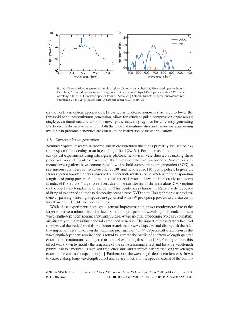
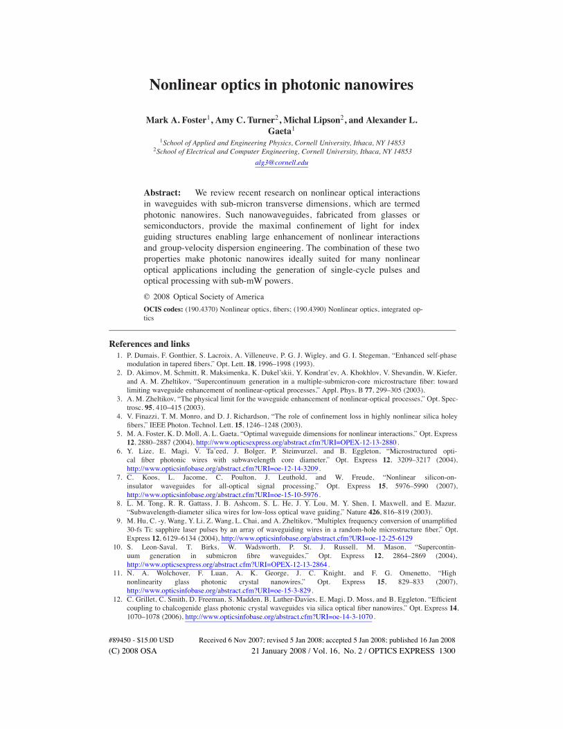
Fig. 6. Supercontinuum generated in silica glass photonic nanowires. (a) Generated spectra from a2-cm long 510-nm diameter tapered single-mode fiber using 600-ps 140-nJ pulses with a 532 centerwavelength [10]. (b) Generated spectra from a 3.5-cm long 650-nm diameter tapered microstructuredfiber using 25-fs 125-pJ pulses with an 820-nm center wavelength [39].
on the nonlinear optical applications. In particular, photonic nanowires are used to lower thethreshold for supercontinuum generation, allow for efficient pulse-compression approachingsingle-cycle durations, and allow for novel phase matching regimes for efficiently generatingUV to visible dispersive radiation. Both the maximal nonlinearities and dispersion engineeringavailable in photonic nanowires are crucial to the realization of these applications.
4.1. Supercontinuum generation
Nonlinear optical research in tapered and microstructured fibers has primarily focused on ex-treme spectral broadening of an injected light field [28–34]. For this reason the initial nonlin-ear optical experiments using silica-glass photonic nanowires were directed at making theseprocesses more efficient as a result of the increased effective nonlinearity. Several experi-mental investigations have demonstrated low-threshold supercontinuum generation (SCG) insub-micron core fibers for femtosecond [37, 39] and nanosecond [10] pump pulses. In general,larger spectral broadeningwas observed in fibers with smaller core diameters for correspondinglengths and pump powers. Still, the maximal spectral extent achievable in photonic nanowiresis reduced from that of larger core fibers due to the positioning of the anomalous-GVD regimeon the short wavelength side of the pump. This positioning clamps the Raman self-frequencyshifting of generated solitons to the nearby second zero-GVD point. Using photonic nanowires,octave-spanning white-light spectra are generated with kW peak pump powers and distances ofless than 2 cm [10, 39], as shown in Fig 6.While these experiments highlight a general improvement in power requirements due to the
larger effective nonlinearity, other factors including dispersion, wavelength-dependent loss, awavelength-dependent nonlinearity, and multiple-stage spectral broadening typically contributesignificantly to the resulting spectral extent and structure. The impact of these factors has leadto improved theoretical models that better match the observed spectra and distinguish the rela-tive impact of these factors on the nonlinear propagation [42–44]. Specifically, inclusion of thewavelength-dependent nonlinearity is found to increase the predicted short-wavelength spectralextent of the continuum as compared to a model excluding this effect [43]. For larger fibers thiseffect was shown to modify the timescale of the self-steepening effect and for long wavelengthpumps lead to a reduced Raman-self frequency shift and therefore a decreased long wavelengthextent to the continuum spectrum [44]. Furthermore, the wavelength dependent loss was shownto cause a sharp long-wavelength cutoff and an asymmetry in the spectral extent of the contin-
#89450 - $15.00 USD Received 6 Nov 2007; revised 5 Jan 2008; accepted 5 Jan 2008; published 16 Jan 2008(C) 2008 OSA 21 January 2008 / Vol. 16, No. 2 / OPTICS EXPRESS 1310
uum for small core diameters [45, 46].Rich propagation dynamics result from the multiple-stage continuum process in tapered mi-
crostructured fibers. In one experiment ultrashort pulses where launched in the anomalous-GVD regime near the first dispersion point of an untapered 2.3-µm core diameter microstruc-tured fiber. The self-phase modulation in the initially untapered fiber lead to the generation ofseveral spectrally separated solitons. Once these solitons reach the sub-µm tapered region, thesolitonic conditions change due to the larger nonlinearity and the modified dispersion. This leadthe initially generated solitons to each undergo further spectral broadening in the tapered re-gion allowing for a greater extent of the supercontinuum particularly in the visible regime [45].While this multiple-stage continuumwas initially demonstrated using photonic nanowires, sim-ilar multiple-stage broadening processes have been shown to increase visible components ofSCG in fibers with cores larger than 1-µm [47–49].
4.2. Pulse compression
Beyond increasing the efficiency of nonlinear processes such as SCG, the use of photonicnanowires allows for propagation in novel dispersive regimes. Typically, for SCG the inputpulse is launched in the anomalous-GVD regime and has a pulse energy corresponding to ahigher-order soliton. The soliton order is given by N =
!LD/LNL, where LD = Tin2/ |#2| is the
dispersion length, LNL = 1/("P0) is the nonlinear length, Tin is the duration of the input pulse,#2 is the GVD at the center wavelength, " is the effective nonlinearity, and P0 is the peak powerof the input pulse. Launching a higher-order soliton allows the propagating pulse to undergosoliton-effect compression [25]. In the initial stages of SCG, the propagating pulse spectrallybroadens and compresses slightly but then inevitably breaks apart into a series of solitonic com-ponents, which has been termed soliton fission [30]. The engineerable dispersion of photonicnanowires allows one to choose the dispersive conditions to maintain the phase overlap of thebroadened spectrum during the initial stages of SCG and thus delay soliton fission. In this way,increased soliton-effect compression is possible. If the photonic nanowire is cut short enoughthat the pulse exits prior to fission, then a compressed pulse is available for further interactionsand measurement [50].To achieve broadband soliton effect compression, one requires a large region of anomalous-
GVD with low third-order dispersion. The GVD engineering available with photonic nanowiresallows for such optimization. Specifically, the use of silica photonic nanowires with diameterson the order of the wavelength of the guided light allows for such a dispersive regime. Futher-more for typical sub-100-fs input pulses, the photonic nanowire length must be on the orderof a millimeter. Operating under these conditions, the propagating pulse is compressed effi-ciently to extremely short durations in the initial stages of spectral broadening and exits thewaveguide before soliton fission. Compression of 70-fs pulses to 6.8 fs pulses has been ex-perimentally demonstrated as shown in Fig 7 and simulations and preliminary measurementspredict single-cycle pulse durations are possible [50,51].While fibers with core diameters largerthan 1-µm also allow for considerable soliton-effect compression, compression factors as largeas those achievable in photonic nanowires are not expected due to the increased third-orderdispersion [52].
4.3. UV-visible dispersive-wave generation
Cherenkov radiation is associated with the generation of optical waves from particles travelingfaster than the speed of light in a material. However, it can also be observed in radiation emittedfrom short pulses of light [30, 53, 54]. This effect has lead to some confusion since pulsesof light certainly cannot travel faster than their own luminal velocity. The Cherenkov typephase-matching results from the definite phase relationship between the propagating pulse and
#89450 - $15.00 USD Received 6 Nov 2007; revised 5 Jan 2008; accepted 5 Jan 2008; published 16 Jan 2008(C) 2008 OSA 21 January 2008 / Vol. 16, No. 2 / OPTICS EXPRESS 1311
Fig. 7. Retrieved few-optical-cycle pulse self-compressed from the 70-fs input pulse by propagationin the 980-nm core diameter and 2-mm-long photonic nanowire pictured above the plot [50].
the emitted radiation, which does not exist for superluminal particles. This phase relationshipallows the pulse to travel at its luminal group velocity but phase-match to dispersive waves inmuch the same way as the superluminal particle.Consider a pulse of light traveling from point A to point B separated by a distance $z. This
pulse of light starts at point A at time t = 0 with a phase of %A = 0. At point A the pulsegenerates a dispersive wave with a phase of %A = 0. The pulse then travels to point B at itsgroup velocity vg and therefore arrives at point B at time t = $t = $z/vg. In traveling to pointB, the pulse accumulates a phase as a result of the distance traversed and the time expired.The phase of the pulse at point B is then %B = n(&p)&p$z/c!&p$t+n2I&p$z/(2c), where nis the index of refraction, n2 is the nonlinear index of refraction, & p is the angular frequencyof the pulse, c is the speed of light, and I is the intensity of the pulse. If this pulse generatesfurther dispersive radiation at point B and time t = $t, this second dispersive wave will havean initial phase of %B. For the generated dispersive radiation to be phase matched, the phaseaccumulated by the dispersive wave traveling from point A to B in time $t must be equal to thephase of the second emitted dispersive wave at point B and time t = $t. This condition leads tothe established phase matching condition of dispersive waves emitted by solitonic pulses [30],that is,
n(&d)&dc
! &dvg
=n(&p)&p
c! &p
vg+n2I&p
2c. (2)
While the ability to phase-match radiation is clear, the connection to Cherenkov radiation isnot as obvious. The essential difference between a particle and the pulse is that the particle emitsradiation with a constant initial phase. In contrast, the dispersive wave generated by the pulseis emitted with an initial phase that is directly related to the accumulated phase of the pulse asit propagates. Furthermore, the dispersive wave that is emitted at point B with an initial phase
#89450 - $15.00 USD Received 6 Nov 2007; revised 5 Jan 2008; accepted 5 Jan 2008; published 16 Jan 2008(C) 2008 OSA 21 January 2008 / Vol. 16, No. 2 / OPTICS EXPRESS 1312
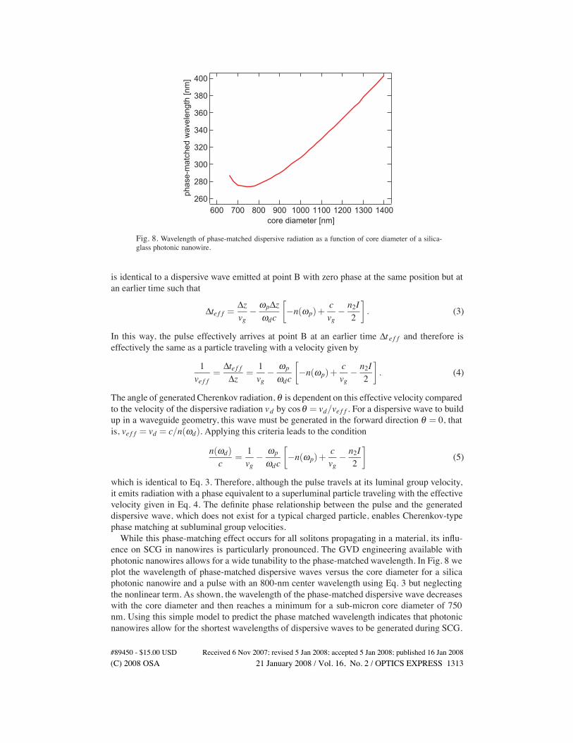
Fig. 8. Wavelength of phase-matched dispersive radiation as a function of core diameter of a silica-glass photonic nanowire.
is identical to a dispersive wave emitted at point B with zero phase at the same position but atan earlier time such that
$te f f =$zvg
!&p$z&dc
"!n(&p)+
cvg
! n2I2
#. (3)
In this way, the pulse effectively arrives at point B at an earlier time $t e f f and therefore iseffectively the same as a particle traveling with a velocity given by
1ve f f
=$te f f
$z=1vg
!&p
&dc
"!n(&p)+
cvg
! n2I2
#. (4)
The angle of generated Cherenkov radiation, ' is dependent on this effective velocity comparedto the velocity of the dispersive radiation vd by cos' = vd/ve f f . For a dispersive wave to buildup in a waveguide geometry, this wave must be generated in the forward direction ' = 0, thatis, ve f f = vd = c/n(&d). Applying this criteria leads to the condition
n(&d)c
=1vg
! &p
&dc
"!n(&p)+
cvg
! n2I2
#(5)
which is identical to Eq. 3. Therefore, although the pulse travels at its luminal group velocity,it emits radiation with a phase equivalent to a superluminal particle traveling with the effectivevelocity given in Eq. 4. The definite phase relationship between the pulse and the generateddispersive wave, which does not exist for a typical charged particle, enables Cherenkov-typephase matching at subluminal group velocities.While this phase-matching effect occurs for all solitons propagating in a material, its influ-
ence on SCG in nanowires is particularly pronounced. The GVD engineering available withphotonic nanowires allows for a wide tunability to the phase-matched wavelength. In Fig. 8 weplot the wavelength of phase-matched dispersive waves versus the core diameter for a silicaphotonic nanowire and a pulse with an 800-nm center wavelength using Eq. 3 but neglectingthe nonlinear term. As shown, the wavelength of the phase-matched dispersive wave decreaseswith the core diameter and then reaches a minimum for a sub-micron core diameter of 750nm. Using this simple model to predict the phase matched wavelength indicates that photonicnanowires allow for the shortest wavelengths of dispersive waves to be generated during SCG.
#89450 - $15.00 USD Received 6 Nov 2007; revised 5 Jan 2008; accepted 5 Jan 2008; published 16 Jan 2008(C) 2008 OSA 21 January 2008 / Vol. 16, No. 2 / OPTICS EXPRESS 1313
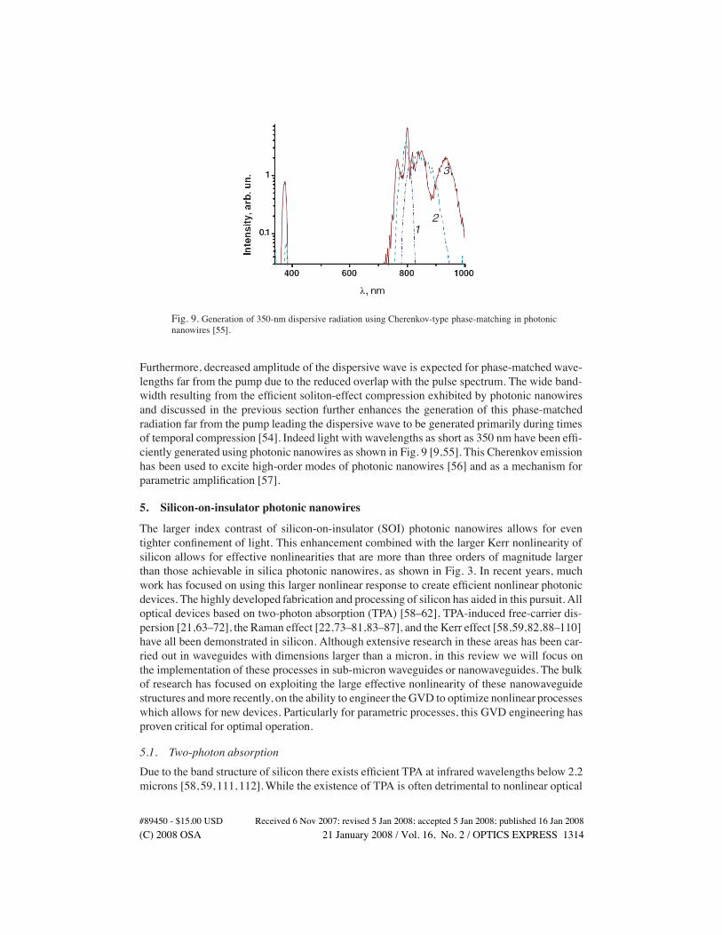
Fig. 9. Generation of 350-nm dispersive radiation using Cherenkov-type phase-matching in photonicnanowires [55].
Furthermore, decreased amplitude of the dispersive wave is expected for phase-matched wave-lengths far from the pump due to the reduced overlap with the pulse spectrum. The wide band-width resulting from the efficient soliton-effect compression exhibited by photonic nanowiresand discussed in the previous section further enhances the generation of this phase-matchedradiation far from the pump leading the dispersive wave to be generated primarily during timesof temporal compression [54]. Indeed light with wavelengths as short as 350 nm have been effi-ciently generated using photonic nanowires as shown in Fig. 9 [9,55]. This Cherenkov emissionhas been used to excite high-order modes of photonic nanowires [56] and as a mechanism forparametric amplification [57].
5. Silicon-on-insulator photonic nanowires
The larger index contrast of silicon-on-insulator (SOI) photonic nanowires allows for eventighter confinement of light. This enhancement combined with the larger Kerr nonlinearity ofsilicon allows for effective nonlinearities that are more than three orders of magnitude largerthan those achievable in silica photonic nanowires, as shown in Fig. 3. In recent years, muchwork has focused on using this larger nonlinear response to create efficient nonlinear photonicdevices. The highly developed fabrication and processing of silicon has aided in this pursuit. Alloptical devices based on two-photon absorption (TPA) [58–62], TPA-induced free-carrier dis-persion [21,63–72], the Raman effect [22,73–81,83–87], and the Kerr effect [58,59,82,88–110]have all been demonstrated in silicon. Although extensive research in these areas has been car-ried out in waveguides with dimensions larger than a micron, in this review we will focus onthe implementation of these processes in sub-micron waveguides or nanowaveguides. The bulkof research has focused on exploiting the large effective nonlinearity of these nanowaveguidestructures andmore recently, on the ability to engineer the GVD to optimize nonlinear processeswhich allows for new devices. Particularly for parametric processes, this GVD engineering hasproven critical for optimal operation.
5.1. Two-photon absorption
Due to the band structure of silicon there exists efficient TPA at infrared wavelengths below 2.2microns [58, 59, 111, 112].While the existence of TPA is often detrimental to nonlinear optical
#89450 - $15.00 USD Received 6 Nov 2007; revised 5 Jan 2008; accepted 5 Jan 2008; published 16 Jan 2008(C) 2008 OSA 21 January 2008 / Vol. 16, No. 2 / OPTICS EXPRESS 1314

Fig. 10. An all-optical switch based on TPA-induced free-carrier dispersion in a siliconnanowaveguide ring resonator. (a) SEM image of the device. (b) Experimental switching realiza-tion [65].
processes, it has proven to be useful for a variety of photonic devices. Using solely TPA, anultrafast switch has been demonstrated in silicon nanowaveguides requiring peak powers of 1.8W for operation [61, 62]. Furthermore, many all-optical devices using silicon nanowaveguideshave made use of TPA-induced free-carrier injection. In this process, the photons absorbedthrough TPA generate free electrons and holes. The presence of these free carriers locally mod-ifies the refractive index and the loss of the silicon structures such that [63],
$n = ! e2! 2
8(2c2)0n
"$Nemce"
+$Nhmch"
#, (6)
$* =e3! 2
4(2c3)0n
"$Ne
mce"2µe+
$Nhmch"
2µh
#, (7)
where $n and $* are the changes in the index of refraction and absorption, respectively, e isthe electronic charge, )0 is the permittivity of free space, n is the inherent refractive index ofcrystalline silicon, mce
" is the conductivity effective mass of electrons, mch" is the conductivity
effective mass of holes, µe is the electron mobility, and µh is the mobility of holes [63]. A majorlimitation of devices based on this effect is speed, and as such photonic nanowires provide anadded advantage. The speed of devices based on carrier effects is generally limited by the free-carrier lifetime. For bulk silicon, the free-carrier lifetime is dependent on the level of doping.As the doping level is increased, the lifetime is reduced but is accompanied by an increasein optical loss. Using typical doping levels for optical purposes, the free-carrier lifetime ofbulk silicon is on the µs time scale. Therefore for silicon devices with large dimensions, thefastest devices based on free-carrier effects are limited to these speeds [64]. This lifetime can bereduced using a number of techniques including sweeping out carriers with a reversed-biasedPIN structure [83] and ion implantation [113]. However, the simplest technique to reduce thecarrier lifetime is to increase the rate of surface recombination. By making the waveguide cross-section smaller, the ratio of surface area to volume increases, and correspondingly the rateof surface recombination increases. Therefore using the smallest possible waveguide cross-sections (ie. photonic nanowires) provides the shortest free-carrier lifetimes and the fastestdevice performance with minimal added complexity.Combining the extremely efficient TPA available in highly confining silicon nanowaveguides
with the reduced free-carrier lifetimes available in nanowaveguides, optical bistability, all-optical switching, and all-optical wavelength conversion have been demonstrated in silicon
#89450 - $15.00 USD Received 6 Nov 2007; revised 5 Jan 2008; accepted 5 Jan 2008; published 16 Jan 2008(C) 2008 OSA 21 January 2008 / Vol. 16, No. 2 / OPTICS EXPRESS 1315

Fig. 11. All-optical pulse delay in a silicon nanowaveguide using stimulated Raman scattering. (a)Picture of the device. (b) Experimental measurement of a 1.3 pulse width delay [87].
nanowaveguides using power levels as low as 10 mW with free-carrier lifetimes of approxi-mately 500 ps. [21, 65, 66, 68–72]. As an example, an all-optical switch based on TPA-inducedfree-carrier dispersive tuning of an microresonator is shown in Fig. 10. By incorporatingreverse-biased PIN structures, free-carrier lifetimes shorter than 50 ps have been reported forthese nanowaveguide all-optical devices [67].
5.2. Raman amplification and oscillation
Silicon exhibits a strong and relatively narrow (#1 nm) Raman response. Using this re-sponse, several Raman-based all-optical devices have been developed for the SOI platform.The achievement of large Raman amplification and Raman oscillation was demonstrated usinglarge waveguide cross-sections and incorporating a PIN diode for CW operation [79, 83–85].A major hurdle to creating a Raman oscillator in silicon was the nonlinear loss resulting fromTPA and TPA-induced free-carrier absorption (FCA). To remove FCA and to lower the powerrequirements for such devices, the use of silicon nanowaveguides can provide a benefit. Asnoted in the previous section, the use of photonic nanowires allows for a reduction in the free-carrier lifetime, which allows not only for faster devices but also reduces the build up of freecarriers leading to lower densities and reduced losses incurred by FCA [76, 77]. Using siliconphotonic nanowires, Raman amplification of 3.1 dB without the need for a reversed-biased PINstructure has been demonstrated using peak pump powers of 2.8 W [22, 78, 80–82].A further application of the efficient Raman process in silicon nanowaveguides has included
slow light [86, 87]. The narrow gain feature induced by the Raman effect creates a rapidlyvarying phase velocity as predicted by the Kramers-Kronig relations. This rapidly varying phasevelocity leads to slow group velocities at the center of the gain feature. Utilizing this effect, all-optical delays of 1.3 pulse widths have been demonstrated in SOI photonic nanowires as shownin Fig. 11 [87].
5.3. Self-phase and cross-phase modulation
The tight confinement of SOI photonic nanowires allows for efficient effects derived from theKerr nonlinearity. These parametric nonlinear processes often depend on the GVD for effi-cient operation. Perhaps the most straightforward parametric process to observe is that of self-phase modulation in which the Kerr-induced phase shift of a propagating pulse causes a red(blue) frequency shift on the front (back) of the pulse [25]. This effect generally character-izes the initial stages of supercontinuum generation discussed previously [34]. In silicon pho-
#89450 - $15.00 USD Received 6 Nov 2007; revised 5 Jan 2008; accepted 5 Jan 2008; published 16 Jan 2008(C) 2008 OSA 21 January 2008 / Vol. 16, No. 2 / OPTICS EXPRESS 1316

0 1 2 3 4 5 60
1
2
3
4
5
6
7
simulationexperiment
outp
ut p
ower
(a.u
.)
Input Peak Power (W)
input
input output
Drop (output)
Pass8 mm
Kerr medium BPF
1548 1550 1552 1554 1556
spec
tral d
ensit
y (5
dB/
div)
1548 1550 1552 1554 1556wavelength (nm)wavelength (nm)
5.6 W3.2 W0.8 W0.2 W
pulse peak power
Fig. 12. All-optical SPM-based regenerator using a silicon nanowaveguide and integrated ring res-onator band-pass filter (BPF). (a) Diagram of the device. (b) Experimental and simulated power trans-fer function. (c) Experimentally measured SPM broadening and filtered output for several pump pow-ers [106].
tonic nanowires, self-phase modulation has been observed for both picosecond and femtosec-ond pulses [98, 101]. Asymmetric spectral broadening is observed due to an additional rapidphase shift from the TPA-generated free-carriers, which aids the blue shift at the back of thepulse but opposes the red shift at the front. Additional spectral characteristics have been identi-fied to result from dispersive-wave generation, from non-negligible third-order dispersion, andfrom soliton-formation [101, 103, 105, 110].With the incorporation of an integrated spectral filter, an all-optical regeneration device has
been demonstrated [106] using silicon nanowaveguides based on the technique originally pro-posed by Mamyshev [114]. A schematic of the device is shown in Fig. 12(a). Signal regen-eration relies upon a nonlinear power transfer through the device typically in the shape of anS-like step function, as shown in Fig. 12(b). This reduces the noise on the 0’s and 1’s of a datastream after being processed through the system. The silicon nanowaveguide device operates at6-W peak powers, which represents an 8-fold reduction from previous integrated SPM-basedtechniques.Cross-phase modulation is comparable to self-phase modulation except that the impact of
the Kerr-induced phase shift occurs on a second generally weaker propagating pulse. Devicesbased on this effect have been demonstrated to be efficient in silicon photonic nanowires, andthe effects of the GVD have been observed to greatly impact the interaction when the pulsesare of significantly different wavelengths [99, 104].
#89450 - $15.00 USD Received 6 Nov 2007; revised 5 Jan 2008; accepted 5 Jan 2008; published 16 Jan 2008(C) 2008 OSA 21 January 2008 / Vol. 16, No. 2 / OPTICS EXPRESS 1317

Fig. 13. Wavelength conversion across four telecommunications bands using four-wave mixing in sil-icon nanowaveguides (a) Conversion efficiency as a function of wavelength. The efficiency is shapedby the combined effects of the GVD and the fourth order dispersion of the nanowaveguide. (b) Exper-imentally observed FWM wavelength conversion from 1477 nm to 1672 nm [107].
5.4. Four-wave mixing
Four-wavemixing in silicon waveguides involves the third-orderKerr nonlinearity. This processhas been shown to be efficient and broadband in silicon provided that the conditions of phase-matching are met [82, 88, 92–97, 100, 107]. Group-velocity dipsersion engineering of siliconphotonic nanowires allows for the zero-GVD point or the anomalous-GVD region to be locatedin the C-band. In waveguides with near-zero-GVD, conversion of continuous-wave light canbe achieved at efficiencies of -10 dB over bandwidths larger than 150 nm [97, 107]. Utilizinghigher-order dispersion to achieve phase-matching wavelength conversion across four telecom-munications bands has been achieved as seen in Fig. 13. In silicon nanowaveguides FWMwavelength conversion requires peak powers of only 100-mW. Furthermore, in a pulsed exper-iment and with waveguides exhibiting anomalous-GVD, it was demonstrated that parametricamplification is achievable with reduced free-carrier lifetimes using peak powers on the order of1 W [95]. This demonstration indicates the potential for a wavelength-agile CMOS-compatiblesource on chip in the form of a FWM-based optical parametric oscillator.Resonant enhancement of FWM has been demonstrated in silicon nanowaveguide ring res-
onators [109]. The addition of a resonant structure further reduces the peak power requiredto observe this nonlinear process. Using input peak powers below 1 mW, FWM wavelengthconversion has been observed in a micrometer-scale silicon nanowaveguide ring resonator. Theability to observe nonlinear interactions at sub-mW power levels in a micrometer-scale devicedemonstrates the potential scalability of nonlinear optical devices on a single photonic chip. Atthese ultra-low power levels and sizes, it is possible to realize hundreds of devices operatingsimultaneously on a single chip.Regeneration devices based on FWM have also been demonstrated in silicon photonic
nanowires [108]. These processes rely on the ultrafast response of the FWM process and onthe quadratic dependence on the pump power. Using a variety of pump and signal configu-rations, reshaping and retiming of actual 10-Gbps return-to-zero and non-return-to-zero datastreams have been demonstrated using average powers of only 30 mW [108].
6. Future directions
As highlighted in the previous sections, extensive research has been carried out on applyingmaximally confining waveguides for nonlinear optical functionality. Nevertheless, many av-enues remain unexplored. The majority of research has investigated nonlinear processes in sil-
#89450 - $15.00 USD Received 6 Nov 2007; revised 5 Jan 2008; accepted 5 Jan 2008; published 16 Jan 2008(C) 2008 OSA 21 January 2008 / Vol. 16, No. 2 / OPTICS EXPRESS 1318

ica glass and silicon nanowaveguides, which is driven by the mature fabrication and broadavailability of these materials. Other materials may have more favorable nonlinear propertiessuch as + (2) responses, a larger + (3) response, or lower linear and nonlinear losses. Researchinto the nonlinear optical properties of photonic nanowires of these materials will undoubtedlyemerge once the challenges of fabrication are overcome. Furthermore, many materials can-not be formed into waveguides. Photonic nanowires have potentially large evanaescent fieldsas seen in the 0.06 µm2 waveguides in Fig. 2. Using the access to the evanescent field avail-able in photonic nanowires, integration of new materials, such as gases, with highly confiningwaveguides is emerging [115]. With these new areas of research, in addition to further applica-tions of silica glass and silicon waveguides, photonic nanowires will continue to provide lowerpower levels and new functionalities to nonlinear optical devices.
6.1. Other materials
Research has begun on the fabrication and application of photonic nanowires from novel glasseswith large nonlinear responses including SF6 and chalcogenides [11,116]. In particular chalco-genide glasses have a nonlinear response which is 2 to 3 orders of magnitude larger than silicaglass and a relatively high linear refractive index. The combination of these two properties al-lows the effective nonlinearity of chalcogenide glass photonic nanowires to be more than 3orders of magnitude larger than silica glass nanowires, which promises the extension of manyapplications of nonlinear optics in optical fibers to more readily achievable power levels. Self-phase modulation has been observed in tapered fibers of SF6 and chalcogenide glasses usingpeak power levels as low as 1 W. Core diameters as small as 400 nm have been achieved inSF6 glass, but nonlinear effects in sub-micron chalcogenide fibers have yet to be reported. Ad-ditionally, dispersion engineering and phase-matching of parametric processes such as FWMhave not been experimentally demonstrated in photonic nanowires of these materials but shouldbe expected in the near future with improved fabrication [116, 117].Other semiconductor materials are also being explored for implementation in nonlinear opti-
cal devices. Nanowaveguides have been fabricated from AlGaAs and GaAs and several demon-strations of efficient nonlinear processes such as self-phase modulation and FWM have beenobserved [16,118–121]. The linear propagation loss of these waveguides has typically impededtheir performance, but with further improvements in the fabrication process this challenge willcertainly be overcome. Dispersion engineering and anomalous-GVD near 1550 nm have re-cently been demonstrated in AlGaAs nanowaveguides [122]. Efficient nonlinear optics usingIII-V nanowaveguides promises new realms of integrated nonlinear optical devices incorpo-rated with optically active III-V devices such as lasers, amplifiers, and modulators.
6.2. Evanescent nonlinearities
A wide variety of useful nonlinear optical materials intrinsically cannot be fabricated as wave-guides such as gases and liquids. Through the potentially large evanescent fields, photonicnanowires provide a route towards incorporating these materials in a high-confinement guided-wave geometry. When the dimensions of a photonic nanowire are reduced slightly below theoptimal confinement point, a large evanescent field is produced, as seen in Fig. 2. For a rangeof sizes, this mostly evanescent mode still has a relatively small mode-field area and thus alarge effective nonlinearity. In Fig. 14 the effective nonlinearity for a silica photonic nanowiresurrounded by an evanescent nonlinear material with an index close to 1 (i.e. a gas) is plot-ted as a function of core diameter for a wavelength of 800 nm. The optimal core diame-ter for evanescent nonlinearities is 340 nm. At this optimal size, the effective nonlinearity ismore than an order of magnitude larger than those currently available in hollow-core photonicbandgap fibers, which is also a promising system for guided-wave integration with nonlinear
#89450 - $15.00 USD Received 6 Nov 2007; revised 5 Jan 2008; accepted 5 Jan 2008; published 16 Jan 2008(C) 2008 OSA 21 January 2008 / Vol. 16, No. 2 / OPTICS EXPRESS 1319

"!
Fig. 14. Effective nonlinearity as a function of core diameter of a silica-glass photonic nanowireassuming a gaseous nonlinear cladding material with a nonlinear index coefficient n2. As a comparisonthe effective nonlinearity of a commercially available 800-nm hollow-core photonic bandgap fiber(Crystal Fiber HC-800-02) with a 5-µmmode field diameter and "!3/n2 = 0.205 is shown by the reddashed line.
gases [123–127]. Interactions with gases have been experimentally demonstrated using silicaglass photonic nanowires [115], and integrated optical nanowaveguides have also been analyzedfor this purpose with novel slot and hole geometries being explored to maximize the evanescentfield strength [7, 128–130].
7. Conclusions
Photonic nanowires allow for maximal effective nonlinearities and a large degree of dispersionengineering. These properties in combination with the potentially large evanescent fields andminimal optical footprint allow such nanowaveguides to be ideally suited for a host of nonlinearoptical interactions and devices. With the incorporation of new materials and the demonstra-tion of novel effects, photonic nanowires should continue to provide unique nonlinear opticalfunctionality at even lower power levels.
Acknowledgements
This work is funded by the Center for Nanoscale Systems, supported by the NSF and the NewYork State Office of Science, Technology and Academic Research, and the DARPA DSO Slow-Light Program.
#89450 - $15.00 USD Received 6 Nov 2007; revised 5 Jan 2008; accepted 5 Jan 2008; published 16 Jan 2008(C) 2008 OSA 21 January 2008 / Vol. 16, No. 2 / OPTICS EXPRESS 1320


![Optics and spectroscopy of gold nanowires€¦ · Priya Vasanthakumar To cite this version: Priya Vasanthakumar. Optics and spectroscopy of gold nanowires. Other [cond-mat.other].](https://static.fdocuments.in/doc/165x107/5ed30ae671c9d22f9b3ae415/optics-and-spectroscopy-of-gold-nanowires-priya-vasanthakumar-to-cite-this-version.jpg)
