Nondestructive and Contactless Characterization Method for Spatial Mapping of the Thickness and
24
Chapter 1 Nondestructive and Contactless Characterization Method for Spatial Mapping of the Thickness and Electrical Properties in Homo-Epitaxially Grown SiC Epilayers Using Infrared Reflectance Spectroscopy Sadafumi Yoshida, Yasuto Hijikata and Hiroyuki Yaguchi Additional information is available at the end of the chapter http://dx.doi.org/10.5772/50749 1. Introduction Silicon carbide (SiC) is one of the most promising semiconducting materials for the fabrica‐ tion of high power electronic devices with extremely low loss, owing to its excellent physical properties, such as high breakdown electric field, high saturation electron drift velocity, and high thermal conductivity. Nowadays, some kinds of devices, such as SBDs, JFETs and MOSFETs have been on the market. For the fabrication of SiC devices with high yield rates, i.e., for reducing the scattering of device specification, the production of high-quality, large- diameter epi-wafers with uniform thickness and electrical properties is indispensable. In or‐ der to characterize the electrical and thickness uniformity of the epi-wafers during the device process, i.e., to know how the thickness, doping concentration and mobility are dis‐ tributed over the SiC epi-layers, it is necessary to develop the characterization method that can perform the determinations of thickness and electrical properties simultaneously in a nondestructive and noncontact way. To characterize the distribution of the electrical properties over SiC wafers and homo-epi- wafers, conductivity mapping is often performed [1]. However, the distribution of carrier concentration and mobility cannot provide from the conductivity mapping, because the con‐ ductivity depends both on the distribution of dopant concentration and the crystallinity and/or distribution of crystal defects. In order to characterize the distribution of carrier con‐ centration and mobility over epi-layers, electrical measurement techniques such as Hall ef‐ © 2013 Yoshida et al.; licensee InTech. This is an open access article distributed under the terms of the Creative Commons Attribution License (http://creativecommons.org/licenses/by/3.0), which permits unrestricted use, distribution, and reproduction in any medium, provided the original work is properly cited.
Transcript of Nondestructive and Contactless Characterization Method for Spatial Mapping of the Thickness and

Chapter 1
Nondestructive and Contactless CharacterizationMethod for Spatial Mapping of the Thickness andElectrical Properties in Homo-Epitaxially Grown SiCEpilayers Using Infrared Reflectance Spectroscopy
Sadafumi Yoshida, Yasuto Hijikata andHiroyuki Yaguchi
Additional information is available at the end of the chapter
http://dx.doi.org/10.5772/50749
1. Introduction
Silicon carbide (SiC) is one of the most promising semiconducting materials for the fabrica‐tion of high power electronic devices with extremely low loss, owing to its excellent physicalproperties, such as high breakdown electric field, high saturation electron drift velocity, andhigh thermal conductivity. Nowadays, some kinds of devices, such as SBDs, JFETs andMOSFETs have been on the market. For the fabrication of SiC devices with high yield rates,i.e., for reducing the scattering of device specification, the production of high-quality, large-diameter epi-wafers with uniform thickness and electrical properties is indispensable. In or‐der to characterize the electrical and thickness uniformity of the epi-wafers during thedevice process, i.e., to know how the thickness, doping concentration and mobility are dis‐tributed over the SiC epi-layers, it is necessary to develop the characterization method thatcan perform the determinations of thickness and electrical properties simultaneously in anondestructive and noncontact way.
To characterize the distribution of the electrical properties over SiC wafers and homo-epi-wafers, conductivity mapping is often performed [1]. However, the distribution of carrierconcentration and mobility cannot provide from the conductivity mapping, because the con‐ductivity depends both on the distribution of dopant concentration and the crystallinityand/or distribution of crystal defects. In order to characterize the distribution of carrier con‐centration and mobility over epi-layers, electrical measurement techniques such as Hall ef‐
© 2013 Yoshida et al.; licensee InTech. This is an open access article distributed under the terms of theCreative Commons Attribution License (http://creativecommons.org/licenses/by/3.0), which permitsunrestricted use, distribution, and reproduction in any medium, provided the original work is properly cited.

fect measurements and capacitance-voltage (C–V) measurements have been widely used.These techniques, however, are disadvantageous as a device fabrication process monitoringtool because they require the formation of electrodes on a sample. By using a mercury probeas an electrode, C–V measurements can be performed without the formation of electrodes ona sample. However, the problems caused by the contamination with mercury contact havebeen pointed out, recently.
Optical measurement techniques such as Raman scattering spectroscopy [2-5], infrared (IR)spectroscopic ellipsometry [6], optical absorption measurements [7] have been used to esti‐mate the carrier concentration in SiC wafers as a nondestructive and contactless method. IRreflectance measurements have been used to estimate the electrical properties of GaAs [8] andSiC [9]. Macmillan et al. [10] reported that the thickness of homo-epitaxially grown SiC wa‐fers can be estimated from the interference oscillations in IR reflectance spectra observed bothbelow and upper frequency ranges of the reststrahlen band (800–1000cm–1 for SiC). Nowa‐days, the reflectance measurements in near IR spectral range (1000–4000cm–1) is widely usedto estimate the thickness of homo-epitaxially grown SiC layers in the SiC device process. Asthe thickness of epilayers used for power devices are in the range from several to several tensμm, the observation of reflectance spectra in near IR spectral range is suitable to analyze theoscillation of reflectance caused by the interference effects of light in the epilayers.
We have developed the method of obtaining the thickness and electrical properties of semi‐conductor wafers and epi-wafers, simultaneously, by using IR reflectance spectroscopy[11-15]. In this paper, we will summarize the development of the method, and will discussthe validity of the electrical properties derived from the IR reflectance by comparing withthose estimated from Hall effect and C–V measurements. Finally, we will show the results ofapplying this method to characterize the electrical activation of impurity and crystallinedamages in the ion-implanted, and post-implantation-annealed SiC epilayers.
2. Characterization method of the electrical properties in SiC wafersusing IR reflectance spectroscopy
2.1. Method of obtaining carrier concentration and mobility from IR reflectancespectroscopy [11,12]
The values of dielectric constants of semiconductors in IR spectral region can be calculatedas a function of wavelength or frequency using the dispersion equation. For the analysis ofIR reflectance spectra, a number of dielectric function models have been proposed [16-20].The classical dielectric function (CDF) model [16], which assumes the damping constant ofthe LO phonon is the same as that of the TO phonon, has been widely used. In the case ofwide bandgap semiconductors with an overdamped plasmon system like SiC, the reflec‐tance spectrum is, however, strongly dependent on LO-phonon damping because the plas‐mon is overdamped and the LO phonon frequency is much higher than the plasma frequencyexcept for heavily doped cases. For these reasons, we have chosen to use the modified classi‐
Physics and Technology of Silicon Carbide Devices4

cal dielectric function (MDF) model taking into account the contribution of the TO phonondamping constant and the LO phonon damping constant independently [17]. Consideringthe contributions from phonons and plasmons, the dielectric constant is given as
ε(ω)=ε∞( ωL 2−ω 2− iΓL ωωT 2−ω 2− iΓT ω
−ωp2
ω 2 + iγpω ) (1)
where ε∞ is the high frequency dielectric constant, ωT and ωL are the TO- and LO-phononfrequencies, respectively, ΓT and Γl are the TO- and LO-phonon damping constants, respec‐tively, γp is the free-carrier damping constant, and ωp is the plasma frequency of the free car‐riers, which is given by
ωp =N e 2
m * ε∞(2)
where N, e, and m* are the free carrier concentration, electron charge, and effective mass, re‐spectively. The free-carrier damping constant γp is the inverse of the scattering time τ andtherefore the free-carrier mobility can be derived using the following relation,
μ =e
m * γp(3)
Assuming that the wafers are uniformed in the depth direction, we used the normal-inci‐dence reflectance of a semi-infinite medium R, which is expressed as
R(ω)=(n −1)2 + k 2
(n + 1)2 + k 2 (4)
where n and k are the optical constants, derived from ε/ε0=(n–ik)2.
The carrier concentration and mobility can be determined by fitting the experimental infra‐red reflectance spectrum with calculated ones. To fit the spectra, we used the least-squaresmethod based on eqs. (1) and (4), where we adopted ωp, γp, and ΓL as adjustable parameters.
2.2. Measurements of IR reflectance spectra of SiC wafers and estimation of electricalproperties [12]
Single crystal wafers of commercially produced n-type (nitrogen doped) 6H-SiC were used.IR reflectance spectra were measured using two Fourier-transform infrared (FTIR) spec‐trometers, JASCO FT/IR–VM7 for the far-infrared region (30–600 cm–1) and JASCO FT/IR670-PLUS for the middle-infrared region (400–2000 cm–1), respectively. For far-infrared re‐flectance measurements, two light sources (a mercury arc-lamp and nichrome light source),
Nondestructive and Contactless Characterization Method for Spatial Mapping of the Thickness and ElectricalProperties in Homo-Epitaxially Grown SiC Epilayers Using Infrared Reflectance Spectroscopy
http://dx.doi.org/10.5772/50749
5

three beam splitters (4, 12, 25 μm thick Mylar films) and a p-DTGS (pyroelectric deuteratedtriglycine sulfate) detector were used. For middle-infrared reflectance measurements, a highintensity ceramic light source, a KBr beam splitter, and a TGS detector were employed. EachIR reflectance spectrum was measured with 1 cm–1 spectral resolution. The light diameterswere 5 mm for far-infrared measurements, and 3 mm for middle-infrared measurements.The measurements were performed for (0001) Si-faces of 6H-SiC wafers at nearly normal in‐cidence. An Al mirror was used as a reflectance reference.
Figure 1. Infrared reflectance spectra measured for 6H-SiC wafers with various carrier concentrations at room temper‐ature (dotted line). The solid lines show the fitted spectra calculated using MDF model. The values of carrier concen‐tration and mobility obtained from fitting to the measured IR spectra are described in the figure [12].
The dotted lines in Figure 1 show the typical infrared reflectance spectra of several 6H-SiCwafers of different carrier concentrations at room temperature. The plasma edges and rest‐strahlen bands appear in the far-IR and middle-IR regions, respectively. We derived the val‐ues of carrier concentration and mobility by the curve fitting of calculated curves to theobserved ones. For the curve fitting, we chose ωp, ΓL, γp as adjustable parameters. For thevalues of the other parameters, we employed those obtained from Raman scattering meas‐urements, ε∞=6.52ε0, ωT=797cm–1, ωL=969.4cm–1, ΓT=2cm–1, and m*=0.35m0 for 6H-SiC[2]. Sincethe light is normally incident on the (0001) face of the samples, these parameters are all forthe modes vibrating perpendicular to the c-axis.
From the curve fitting analysis, we obtained a good fit for each experimental spectrum,which was obtained by measuring nine samples with carrier concentrations in the range of4×1017~3×1019cm–3. The solid lines in Figure 1 show examples of the fitted curves obtained byfitting to the typical IR reflectance spectra shown as the dotted line in each figure. The free-
Physics and Technology of Silicon Carbide Devices6

carrier concentration and drift mobility were derived from the best-fit parameters of ωp andγp using eqs.(2) and (3), mentioned above. The values of free-carrier concentration and mo‐bility obtained are also given in each figure.
As shown in Figure 1 (c), there is a slight discrepancy at approximately 900 cm–1 between thespectrum observed and that calculated using the MDF model (eq. (1)). This discrepancy in‐creases with increasing carrier concentration in the high 1019 cm–3 range. For heavily dopedSiC crystals, the CDF and MDF models would be inappropriate because the MDF model isderived considering the effects of phonons and plasmons independently. In the case ofheavily doped SiC crystals, the plasma frequency is closed to the phonon frequency and theLO phonon and plasmon are strongly coupled. Therefore, though the MDF mode can ap‐proximately estimate the electrical properties of heavily doped SiC wafer, it is necessary touse another dielectric function mode that takes into account the effect of LO phonon-plas‐mon coupled modes [19,20] to obtain more accurate values.
2.3. Comparison with the values derived from Hall effect measurements [12]
For the confirmation of the validity of the values of carrier concentration and mobility de‐rived from IR reflectance spectra, we performed Hall effect measurements for the same sam‐ples used for IR reflectance measurements and compared between the values obtained fromthe optical and electrical methods. The 6H-SiC wafers with a wide variety of carrier concen‐trations ranging from 3.4×10¹⁷ to 2.4×1019cm–3 were used.
We cut the SiC wafers to a size of 5×5 mm2 for the Hall effect measurements using van derPauw method. After chemical cleaning, ohmic contacts were fabricated at the corners of eachsample by the evaporation of nickel and subsequent heat treatment at 1000°C for 10 min. IRreflectance measurement and Hall measurement were carried out at room temperature.
Figure 2. Comparison of (a) carrier concentration and (b) mobility values, NIR, μIR obtained from IR reflectance spectro‐scopy measurements with those from Hall effect measurements, NHall, μHall. The broken lines represent the case of com‐plete agreement with each other [12].
Nondestructive and Contactless Characterization Method for Spatial Mapping of the Thickness and ElectricalProperties in Homo-Epitaxially Grown SiC Epilayers Using Infrared Reflectance Spectroscopy
http://dx.doi.org/10.5772/50749
7
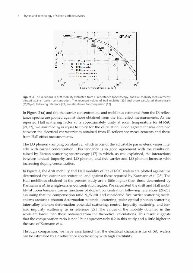
Figure 3. The variations in drift mobility evaluated from IR reflectance spectroscopy, and Hall mobility measurementsplotted against carrier concentration. The reported values of Hall mobility [23] and those calculated theoretically(NA/ND=0) following reference [24] are also shown for comparison [12].
In Figure 2 (a) and (b), the carrier concentrations and mobilities estimated from the IR reflec‐tance spectra are plotted against those obtained from the Hall effect measurements. As thereported Hall scattering factor rH is approximately unity at room temperature for 6H-SiC[21,22], we assumed rH is equal to unity for the calculation. Good agreement was obtainedbetween the electrical characteristics obtained from IR reflectance measurements and thosefrom Hall effect measurements.
The LO phonon damping constant ΓL, which is one of the adjustable parameters, varies line‐arly with carrier concentration. This tendency is in good agreement with the results ob‐tained by Raman scattering spectroscopy [17] in which, as was explained, the interactionsbetween ionized impurity and LO phonon, and free carrier and LO phonon increase withincreasing doping concentration.
In Figure 3, the drift mobility and Hall mobility of the 6H-SiC wafers are plotted against thedetermined free carrier concentration, and against those reported by Karmann et al [23]. TheHall mobilities obtained in the present study are a little higher than those determined byKarmann et al. in a high-carrier-concentration region. We calculated the drift and Hall mobi‐lity at room temperature as functions of dopant concentration following references [24-26],assuming that the compensation ratio NA/ND=0, and considered five carrier scattering mech‐anisms (acoustic phonon deformation potential scattering, polar optical phonon scattering,intervalley phonon deformation potential scattering, neutral impurity scattering, and ion‐ized impurity scattering) as in reference [29]. The values of the mobility obtained in thiswork are lower than those obtained from the theoretical calculations. This result suggeststhat the compensation ratio is not 0 but approximately 0.2 in this study and a little higher inthe case of Karmann et al.
Through comparison, we have ascertained that the electrical characteristics of SiC waferscan be estimated by IR reflectance spectroscopy with high credibility.
Physics and Technology of Silicon Carbide Devices8

2.4. Spatial mapping of the electrical properties over SiC wafers [11,12]
To demonstrate the capability of the method proposed, we performed the spatial mappingof the distribution of the carrier concentration and mobility of a commercially produced 2inch 6H-SiC wafer. For the spatial mapping, we employed a micro FTIR (JASCO IrtronIRT-30 infrared microscope), which was equipped with a mercury cadmium telluride (MCT)detector. The diameter of the beam was 0.1 mm and the interval between measured pointswas 5 mm (a total of 120 measurement points). We performed the measurements in the spec‐tral range of 560–2000 cm–1 with a spectral resolution of 4cm–1.
Figure 4 shows an example of the spatial distribution of the free-carrier concentration andmobility of a commercially produced 2-inch 6H-SiC wafer obtained using this technique.This measurement technique needs no prior surface treatment, because the native oxide lay‐er thickness and surface roughness are not more than 3 nm and their influence on the reflec‐tance spectra is negligible in IR region. The uniformity of free-carrier concentration andmobility throughout this wafer except for 5 mm from the edge were estimated to be approx‐imately ±9% and ±15%, respectively. The free-carrier concentration mapping shows that thefree-carrier concentration in the central region is greater than that in the edge region. On theother hand, the mobility mapping shows the negative correlation of the mobility distribu‐tion with that of carrier concentration. When conductivity mapping is used as the methodfor the mapping of electrical properties of the wafer, it leads to the misleading conclusionthat the electrical uniformity over the wafers is approximately ±5% and the wafer is almostuniform, because the conductivity is determined as the product of carrier concentration andmobility. Therefore, the proposed IR reflectance spectroscopic method is more appropriatefor the characterization of the distribution of the electrical properties of SiC wafers.
Figure 4. Spatial mapping of (a) carrier concentration and (b) mobility in a commercially produced 2 inch 6H-SiC wafer[12].
Nondestructive and Contactless Characterization Method for Spatial Mapping of the Thickness and ElectricalProperties in Homo-Epitaxially Grown SiC Epilayers Using Infrared Reflectance Spectroscopy
http://dx.doi.org/10.5772/50749
9
3. Characterization method of the electrical properties and thickness ofepilayers using IR reflectance spectroscopy
3.1. Method of obtaining the carrier concentration, mobility, and thickness of epilayers,simultaneously [13]
In this section, we propose the method for the simultaneous determination of the electricalproperties, i.e., free carrier concentration and mobility, and the thickness of epilayers as wellas bulk layer by IR reflectance measurements. First, we will explain the procedure of obtain‐ing carrier concentration, mobility and thickness of the epilayers on SiC wafers. Then, wewill compare the electrical properties derived from the IR reflectance analyses with thosefrom Hall effect measurements for n-type epilayers grown on p-type substrates, and withthose from C–V measurements in the case of n-type epilayers on n-type substrates. Finallywe will discuss the validity of the obtained values from the proposed method.
The carrier concentration and mobility of epilayers and substrates, as well as the thicknessof the epilayers can be determined simultaneously by fitting the calculated reflectance spec‐tra to measured ones. The reflectance R from an air/ epilayer/substrate structure at normalincidence is given by
221 2
21 2
2,1
i
i
r r e ndR wherer r e
d
d
pdl
-
-
+= =
+(5)
where r1 and r2 are the Fresnel reflection coefficients at the air/epilayer and the epilayer/substrate interface, respectively, and δ is the phase shift of light in the epilayer, n and d arethe refractive index and the thickness of epilayer, respectively, and λ is wavelength. The op‐tical constants of SiC in IR spectral range are derived from the dielectric constants as a func‐tion of the frequency of the incident light, given by eq.(1) both for substrate and epilayer. Asin the case of SiC bare wafers written in Section 2, we fitted the calculated spectrum to themeasured one by adjusting the values of ωp, γp, ΓT and ΓL of the epilayer and those of thesubstrate, and the epilayer thickness d. From these values, we can obtain the carrier concen‐tration N and mobility μ of the epilayer and substrate using eqs. (3) and (4). In the calcula‐tion, we adopted the values ε∞=6.56, ωT=798cm–1, ωL=970cm–1, and m*
MG=0.58m0, m*MK =0.31m0,
obtained from the Raman scattering measurements of 4H-SiC [2] and optical detection of cy‐clotron resonance (ODCR) [27]. Considering that the free carriers distribute themselves inproportion to the square root of each effective mass, the averaged effective mass, m*=(m*
MKm*MG)1/2, and m*=(1/m*MK
1/2+1/m*MG1/2)/(1/m*MK
3/2+1/m*MG3/2) were used for the calculation
of the carrier concentration and mobility, respectively.
Physics and Technology of Silicon Carbide Devices10

3.2. Measurements of IR reflectance spectra and derivation of electrical properties andthickness of SiC epi-wafers [13]
Samples used in this study were nitrogen doped n-type 4H-SiC epilayers grown on n- and p-type 4H-SiC substrates supplied from National Institute of Advanced Industrial Science andTechnology (AIST). The epilayers were grown on 4H-SiC (0001) Si face 8 off substrates bychemical vapor deposition (CVD). The details of the epilayer growth have been describedelsewhere [28]. In the case of the n-type epilayers on p-type substrates, the carrier concentra‐tion of the epilayers was in the range between 3×10¹⁷ and 2×1018 cm–3, and that of the sub‐strates was typically 4×1016 cm–3. On the other hand, in the case of the n-type epilayers on n-type substrates, the net doping concentration (ND– NA) of the epilayers was in the rangebetween 1×10¹⁷ and 8×1017 cm–3, and that of the substrates was typically 5×1018 cm–3. Thethickness of the epilayers were 6~7 μm, measured by scanning electron microscope (SEM)observation of the cleaved facet of the samples. The IR reflectance spectra in the frequencyrange of 80–2000 cm–1 were measured at room temperature using same spectrometers men‐tioned in Section 2.2. Hall effect measurements were performed at room temperature usingvan der Pauw method for n-type epilayers on p-type substrates. Ohmic contacts were fabri‐cated on the epilayer surfaces by the electron beam evaporation of Ni and subsequent an‐nealing at 900°C for 30min in N2 atmosphere. C–V measurements were performed at roomtemperature using a mercury probe as a Schottky contact.
100
80
60
40
20
0
Ref
lect
ance
(%)
2000150010005000
Wave number(cm-1
)
Nsub = 2.6!1016
cm-3
sub = 60 cm2/(V·s)
Nepi = 3.2!1017
cm-3
epi = 296 cm2/(V·s)
d = 6.6 µm
Experiment
Fitted curve
Figure 5. IR reflectance spectrum of an n-type epilayer on a p-type substrate at room temperature denoted by dashedline. The solid line shows the fitted curve calculated using the MDF model. The values estimated from this fitting arelisted in the figure [13].
Nondestructive and Contactless Characterization Method for Spatial Mapping of the Thickness and ElectricalProperties in Homo-Epitaxially Grown SiC Epilayers Using Infrared Reflectance Spectroscopy
http://dx.doi.org/10.5772/50749
11

At first, we estimated the carrier concentration and mobility of n-type epilayers on p-type sub‐strates from the reflectance measurements, and compared with these values obtained fromHall effect measurements. Figure 5 shows typical IR reflectance spectra measured for the n-type epilayers on p-type substrates. The solid line denotes the calculated values fitted to theexperimental one shown as the dashed line. The values Nepi = 3.2×1017 cm–3, μepi = 296 cm2/(Vs), and d = 6.60 μm were obtained by a curve fitting analysis. These values are listed in thefigure. In the case of p-type substrate whose carrier concentration is low in general, the reflec‐tance spectrum is almost independent of the electrical properties of the substrate, thus, it isdifficult to estimate the carrier concentration and mobility of the substrate. Therefore, weused the values for the p-type substrate without epilayer obtained from the Hall effect meas‐urements. The thickness of the epilayers obtained from the IR reflectance measurements andthose measured from the SEM observation coincide with each other within ±1%.
The carrier concentrations and mobilities obtained from the IR reflectance measurementsare plotted with respect to those obtained from Hall effect measurements in Figures 6 (a)and (b), respectively. Since the Hall scattering factor rH is reported to be approximately uni‐ty at room temperature for 4H-SiC [27,29] as in the case of 6H-SiC, we directly comparedthe drift mobilities estimated from the IR reflectance measurements and those of the Hallmobilities obtained from the Hall effect measurements. The error bars shown in the fig‐ures represent the accuracy of the fitting analysis, and the accuracy is about ±4% for boththe carrier concentration and the mobility, whereas the accuracy of the values derived fromHall effect measurements is about ±10%. As can be seen from these figures, the electricalproperties obtained from the reflectance spectra are in good agreement with those ob‐tained from the Hall effect measurements. These results suggest that the proposed meth‐od is valid for obtaining the values of carrier concentration and mobility of the epilayers.However, careful observation confirms that the values of carrier concentration and mobili‐ty derived from the infrared reflectance measurements are slightly lower than those ob‐tained from the Hall effect measurements. The difference can be explained by theconsideration that the part of free carriers trapped in defects or bounded by dopants can‐not follow in the THz frequency range used for the reflectance measurements, unlike inHall effect measurements, where a direct current is supplied.
Next, we estimated the values of carrier concentration and mobility for n-type epilayers onn-type substrates from the IR reflectance spectra measured. Figure 7 shows a typical IR re‐flectance spectrum observed and its fitted curve. The values Nepi = 1.3×1017 cm–3, μepi = 403cm2/(V s) and d = 4.45 μm; and Nsub = 7.1×1018 cm–3, μsub = 53 cm2/(V s) were obtained by curvefitting analysis as the parameters of the epilayer and substrate, respectively. The accuracy ofthe carrier concentration and mobility of epilayerss derived from the fitting of the IR reflec‐tance spectrum is about ±10%. In Figure 8, the free carrier concentration estimated from theIR reflectance spectra is plotted with respect to the net doping concentrations ND– NA de‐rived from C–V measurements. We calculated the free carrier concentrations n from the netdoping concentrations using
Physics and Technology of Silicon Carbide Devices12

n(T ) + NA =N (h )
1 + {gn(T ) / NC}exp ΔE (h ) / kBT +N (k )
1 + {gn(T ) / NC}exp ΔE (k ) / kBT (6)
NC =2MC( m*d .s . kBT2πℏ2 )3/2
(7)
6
810
17
2
4
6
810
18
2
4
NF
TIR
(cm
-3)
6 7 8 9
1017
2 3 4 5 6 7 8 9
1018
2 3 4
NHall (cm-3
)
(a)
400
300
200
100
FT
IR [
cm
2/(
V·s
)]
400300200100
Hall [cm
2/(V·s)]
(b)
Figure 6. Values of (a) carrier concentration and (b) mobility estimated from IR reflectance measurements and Halleffect measurements. The dotted line in the figures corresponds to the case of complete agreement with each other[13].
Nondestructive and Contactless Characterization Method for Spatial Mapping of the Thickness and ElectricalProperties in Homo-Epitaxially Grown SiC Epilayers Using Infrared Reflectance Spectroscopy
http://dx.doi.org/10.5772/50749
13

100
80
60
40
20
0
Ref
lect
ance
(%
)
2000150010005000
WaveNumber (cm-1
)
Nsub = 7.1!1018
cm-3
µsub = 53 cm2/(V·s)
Nepi = 1.3!1017
cm-3
µepi = 403 cm2/(V·s)
d = 4.45 µm
Experiment Fitted Curve
Figure 7. IR reflectance spectrum of an n-type epilayer on an n-type substrate denoted by dashed line. The solid lineshows the fitted curve calculated using the MDF model. The values estimated from this fitting analysis are listed in thefigure [13].
4
6
810
17
2
4
6
810
18
2
4
NF
TIR
(cm
-3)
6 7 8 9
1017
2 3 4 5 6 7 8 9
1018
2 3 4
ND – NA (cm-3
)
calculated free carrier concentration
for NA/ND = 0
Figure 8. Values of the carrier concentration estimated from the IR reflectance for n-type epilayers on n-type sub‐strates as a function of dopant concentration obtained from C–V measurements for each sample. The solid line repre‐sents the theoretical carrier concentration for T=300K assuming zero doping concentration (NA=0) using eq. (6). Thedashed line represents NFTIR=ND–NA [13].
Physics and Technology of Silicon Carbide Devices14
where kB is the Boltzmann constant, T is the temperature, NA is the concentration of accept‐ors, and N(h) and N(k) are the concentrations of the nitrogens occupied at hexagonal and cu‐bic lattice sites, respectively. Since the number of hexagonal sites is equal to those of cubicsites for 4H-SiC, the donor concentration ND is given by N(h) + N(k). The values of ΔE(h)andΔE(k) are the ionization energies of the nitrogen donor at hexagonal and cubic latticesites, respectively, and g = 2 is the spin degeneracy factor. Equation (7) gives the effectivedensity of states, where Mc = 3 is the number of equivalent conduction band minima, andm*
d.s. is the density-of-states effective mass. The values of ΔE(h) and ΔE(k) were set as 50meV and 100 meV, respectively, referring to the reported experimental data [30,31]. The val‐ues of m*
MΓ = 0.58m0, m*MK = 0.31m0, m*
ML = 0.33m0 derived from ODCR measurements [27]were adopted. The solid line in Figure 8 shows the free carrier concentrations calculated as afunction of the net doping concentration, where we assumed that NA/ ND = 0 or ND / (NA +ND) = 1, because the epilayers we measured are hardly compensated [32]. The values ob‐tained from the IR reflectance spectra are slightly lower than the calculated values, as in thecase for the samples of n-type epilaers on p-type substrates. The value of drift mobility cal‐culated in consideration of five carrier scattering mechanisms [24] is 340 cm2/(Vs), in the caseof NA/ ND = 0 and ND –NA =2.7×1017cm–3, which is almost the same as the value obtained fromthe IR reflectance spectrum, i.e., 403 cm2/(Vs). This result also indicates that the compensa‐tion of the sample is low.
3.3. Extension of the carrier concentration range down to 1016cm–3 order using Terahertzfrequency range [14]
We have shown that the carrier concentration and mobility of substrate and epilayers aswell as the thickness of epilayer are obtained simultaneously from IR reflectance spectra inthe frequency range of 80–2000cm–1, and confirmed that the values of the carrier concentra‐tion, mobility and epilayer thickness estimated from IR reflectance spectroscopy are valid.However, it was difficult to estimate the electrical properties of homo-epilayers with carrierconcentrations less than 1×1017 cm–3 without IR reflectance spectra less than 80 cm–1. Figure 9is the variation of plasma frequency with carrier concentration calculated from eq.(2) for 4H-SiC. The figure indicates the plasma frequencies are smaller than 100cm–1 for the carrier con‐centration less than 1017 cm–3. Figure 10 shows the variations of the reflectance spectrum ofepilayers with the decrease of carrier concentrations from 3×10¹⁸ to 3×1016cm–3. The magni‐fied features of the calculated reflectance spectra for 1×1017cm–3, 5×10¹⁶, and 1–5×1015cm–3 inTerahertz frequency range are shown in Figure 11. These figures suggest that it is necessaryto measure a spectrum down to around 20cm–1 for extending the carrier concentration downto the order of 1016 cm–1.
From these considerations, we extended the spectral range of the reflectance measurementsdown to 20 cm–1 (0.6 THz) by using terahertz reflectance spectroscopy to be able to apply themethod for epilayers with the carrier concentrations in the range of 1016 cm–3. Also we havecompared the free carrier concentrations estimated from reflectance measurements with thenet doping concentrations obtained from C–V measurements to discuss the validity of thischaracterization method.
Nondestructive and Contactless Characterization Method for Spatial Mapping of the Thickness and ElectricalProperties in Homo-Epitaxially Grown SiC Epilayers Using Infrared Reflectance Spectroscopy
http://dx.doi.org/10.5772/50749
15

Samples used in this study were nitrogen doped n-type 4H-SiC epilayers grown on n-type4H-SiC substrates by chemical vapor deposition (CVD) [28]. The net doping concentration(ND– NA) of the epilayers was in the range between 5×10¹⁶ and 1×1018 cm–3, and that of thesubstrates was typically 5×1018 cm–3. The thickness of the epilayers was 6–7 μm, measured bySEM observation. C–V measurements were performed using gold electrodes evaporated onthe samples as Schottky contacts. The reflectance spectra were measured at room tempera‐ture for the spectral region of 20–100 cm–1, 80–600 cm–1 and 540–2000 cm–1 using terahertztime-domain spectroscopy (THz-TDS) (Aispec: pulse IRS 1000/2000), FTIR spectrometers(JASCO: IR-VM7) and (JASCO: Irtron IRT-30), respectively.
1016! 1017! 1018! 1019!
101!
103!
102!
1!
1015!
Carrier Concentration N (cm-3)!
Pla
sma
Fre
quen
cy !
p (c
m-1
)!
Wav
elen
gth!"!
(µm
) !
103!
102!
101!
1!
Figure 9. Variation of plasma frequency ωp with carrier concentration N.
Nepi=3!1016cm-3!
Nepi=1!1017cm-3!
Nepi=3!1017cm-3!
Nepi=1!1018cm-3!
Nepi=3!1018cm-3!
Figure 10. Calculated reflectance spectra of the SiC epilayers (3μm thick) with various carrier concentrations on a SiCwafer (Nsub=5.5×10¹⁸, μsub=50cm2/Vs).
Physics and Technology of Silicon Carbide Devices16

Nepi=1~10!1015cm-3
Nepi=1!1017cm-3
Nepi=5!1016cm-3
Ref
rect
ance
(
! )
Wave Number (cm-1)!
Figure 11. Calculated reflectance spectra of the SiC epilayers (5μm thick) with low carrier concentrations on a SiC wa‐fer (Nsub=4×1018cm–3, μsub=50cm2/Vs).
Figure 12. Measured and calculated reflectance spectra of an n-type epilayer on an n-type substrate at room temper‐ature. The values estimated from this fitting analysis are listed in the figure [14].
We have estimated the values of carrier concentration and mobility for the samples of n-typeepilayers on n-type substrates from the IR reflectance spectra measured. Figure 12 shows themeasured and calculated reflectance spectra of the epilayer with a net doping concentrationaround 5×1016 cm–3 at room temperature. As shown in the figure, reflectance spectrum meas‐ured by THz reflectance spectroscopy are well connected with that measured by IR reflec‐tance spectroscopy at around 100 cm–1, and we obtained a good fit between the measured andthe calculated spectrum. From the values of fitting parameters, the values Nepi = 3.2×1016 cm–3,μepi = 562 cm2/(V s) and d = 6.14 μm, and Nsub = 6.8×1018 cm–3, μsub = 63 cm2/(V s) were obtained.
In Figure 13, the free carrier concentrations estimated from the IR reflectance spectra areplotted against the net doping concentrations ND– NA derived from C–V measurements. Wecalculated the free carrier concentrations n from the net doping concentrations using eq.(6).The solid line in the figure shows the free carrier concentrations calculated as a function ofnet doping concentration. We assumed that NA/ ND = 0 or ND / (NA + ND) = 1, because theepilayers we measured are hardly carrier-compensated [32]. The values obtained from the
Nondestructive and Contactless Characterization Method for Spatial Mapping of the Thickness and ElectricalProperties in Homo-Epitaxially Grown SiC Epilayers Using Infrared Reflectance Spectroscopy
http://dx.doi.org/10.5772/50749
17

reflectance spectra are in fairly good agreement with solid line, suggesting that the values ofthe carrier concentrations estimated from IR reflectance spectra have a sufficient validity.However, a careful look confirms that the values of carrier concentration derived from thereflectance measurements are slightly lower than those estimated from the electrical meas‐urements as in the case of carrier concentrations higher than 1017cm–3. The same tendencywas observed in the comparisons with the Hall effect measurements for the samples of n-type epilayers on p-type substrates as shown in Figure 8. This tendency is considered to bepartly because of the adoption of inappropriate effective mass values for the calculation ofreflectance spectra. It is also considered as a cause that the part of free carriers trapped in thedefects or bounded by dopants cannot follow in the THz frequency range used for the re‐flectance measurements, as mentioned above.
4. Characterization of electrical properties and residual crystallinedamage in ion-implanted and post-implantation-annealed 4H-SiCepilayers using IR reflectance spectroscopy
4.1. Method of obtaining the electrical properties and crystalline damage in ion-implanted SiC epilayers [15]
Ion implantation is an indispensable process for selective area doping into crystalline siliconcarbide (SiC), because the doping of impurities by thermal diffusion is hard to apply for SiCdevice process due to very small diffusion constant of impurities in SiC. After the ion im‐plantation, annealing at high temperatures is necessary for activating the dopants electrical‐ly as well as recovering the crystallinity of SiC damaged by ion implantation. Hall effectmeasurements, secondary ion mass spectroscopy (SIMS) and transmission electron micro‐scopy (TEM) have been widely used to characterize the electrical properties, depth profile ofthe impurities and crystalline damage of implanted layers, respectively. These techniquesare, however, inappropriate to use as device process monitoring tools because Hall effectmeasurement requires the formation of electric contacts, and SIMS and TEM observationsresult in the destruction of the samples. Recently, the short period and high temperature an‐nealing is used in SiC device process [35]. To make clear the effect of short period high-tem‐perature annealing, we investigated the annealing period dependence at the annealingtemperature of 1700°C.
Recently, it has been reported that the crystalline damage induced by ion implantation af‐fects the infrared (IR) reflectance spectra around the reststrahlen region (~800–1000 cm–1)[33,34], and the difference of carrier concentration between epitaxial layer and substrate in‐duces the interference oscillation in the near IR region (1000–4500 cm–1). In this study, weperformed the IR reflectance measurements in the spectral range between 600 and 8000 cm–1
for high-dose phosphorus ion implanted and post-implantation-annealed 4H-SiC wafers tocharacterize both the electrical properties and crystalline damage of the implanted layerswithout destruction and contactless.
Physics and Technology of Silicon Carbide Devices18

Figure 13. The carrier concentration estimated from the reflectance spectra for an n-type epilayer on an n-type sub‐strate as a function of doping concentration obtained from C–V measurements for each sample. The solid line repre‐sents the theoretical carrier concentration for T=300K assuming zero doping concentration (NA=0) using eq. (6). Thedotted line represents NFTIR=ND–NA as a guide to the eye [14].
4.2. High-dose phosphorus ion implantation, post-implantation annealing and IRreflectance measurements [15]
The samples used in this study were 4H-SiC (0001) substrates with p-type ~5 μm thick com‐mercially produced epitaxial layers. The multi-energy implantations of phosphorus ions at500°C were carried out through the 10 nm thick oxide film in six steps (40–250 keV) in orderto form a box-shaped profile with a thickness of 0.3 μm. The total implanted dose was 7×10¹⁵
cm–2. After removing the oxide film by HF, the post implantation annealing was conductedin Ar atmosphere. To investigate the annealing temperature dependence of crystalline re‐covery and electrical properties in the implanted layers, the samples were annealed for 30min at different temperatures of 1200°C, 1300°C, and 1400°C. In addition, to apply the IR re‐flectance analysis to the short-period high-temperature annealing process, we also carriedout the post implantation annealing at 1700°C for various periods between 0.5 and 10 min.IR reflectance measurements were carried out at room temperature on nearly normal inci‐dence using a micro FT-IR spectrometer (light beam diameter was 0.1 mm). The spectral res‐olution and range were 4 cm–1 and 600–8000 cm–1, respectively.
4.3. Analysis of carrier concentration, mobility and crystalline damage from IR reflectancespectra [15]
Figure 14 shows the annealing temperature dependence of IR reflectance spectrum. For as-implanted samples, the reflectivity maximum and the shape in the reststrahlen band de‐creases and becomes blunt, respectively, as compared to those of unimplanted samples.After the high temperature annealing, the reflectivity maximum in the reststrahlen band re‐covers to that of unimplanted samples. This is resulted from the crystalline recovery in im‐planted layer. In the spectral range above ~2000 cm–1, the evident interference oscillation isobserved. It indicates that the implanted dopants are activated and the refractive index of an
Nondestructive and Contactless Characterization Method for Spatial Mapping of the Thickness and ElectricalProperties in Homo-Epitaxially Grown SiC Epilayers Using Infrared Reflectance Spectroscopy
http://dx.doi.org/10.5772/50749
19

implanted layer is changed by the change of carrier concentration. We can see the tendenciesthat the reflectance around 1000 cm–1 becomes larger with increasing the annealing tempera‐ture. We analyzed the observed spectra to evaluate the damage of the ion implantation lay‐ers assuming that the implanted layers are composed of two phases, recrystallized SiCphase and defective SiC phase. We have derived the effective dielectric constants εeff of im‐planted layers using an effective medium approximation (EMA) [33],
0= (1− f )εc −εeff
εc + 2εeff+ f
εd −εeffεd + 2εeff
(8)
1000! 2000 3000 4000
80!
60!
40!
20!
0!
100
Ref
lect
ance
(!
)!
Annealing for 30 minutes!
Wavenumber (cm-1) !
Figure 14. The IR reflectance spectra obtained from the 4H-SiC wafers high-dose implanted and post implantationannealed for 30 minutes [15].
undamaged surface layer!
carrier-concentration-plateau layer!
defective SiC phase!
graded-carrier-concentration layer!
recrystalized SiC phase!
dimpla!
Figure 15. The structural model of the ion implanted SiC wafers used in the calculation of reflectance spectra [15].
Physics and Technology of Silicon Carbide Devices20

2000! 4000! 6000! 8000!
80!
60!
40!
20!
0!
100
Ref
lect
ance
(!
)!
Wavenumber (cm-1)!
Figure 16. Observed (dotted line) and fitted IR reflectance spectra (solid line) for the samples annealed at 1400℃ for30 min. The best fit parameters are described in the figure [15].
where εc and εd are the dielectric constants of re-crystallized and damaged phases, respec‐tively, and f is the volume fraction of damaged phase. We assumed that the frequency de‐pendence of both the dielectric constants of re-crystallized phase and defective phasefollows the MDF model given by eq.(1). Referring to the result of TEM observations, we em‐ployed the structural model that the ion implanted layer is composed of 3 layers: an undam‐aged surface layer, a carrier-concentration- plateau layer, and a graded-carrier-concentrationlayer as shown in Figure 15. Furthermore, we assumed that the volume fraction of defectivephase in a graded-carrier-concentration layer is same as that in a carrier-concentration-pla‐teau layer. For a graded-carrier- concentration layer, we used the multi-layer structure ap‐proximation assuming that the free carrier concentration decreases exponentially with depthand the mobility changes in inverse proportion to carrier concentration.
4.4. Annealing temperature dependences of electrical activity and re-crystallization [15]
As an example of curve fitting analysis, the spectrum of the sample annealed at 1400°C for30 min and the fitted curve are show in Figure 16. We obtained a good fit in the whole spec‐tral region measured. The best-fit parameters derived are also described in the figure. Figure17 (a) shows the annealing temperature dependence of the volume fraction of the defectivephase. By post implantation annealing, the volume fraction of defective SiC drastically de‐creases from 92 % (as implanted) to 2.9 % (1200°C annealed), and decreases a little with in‐creasing of annealing temperature up to 1400°C. Figure 17 (b) shows the annealingtemperature dependence of the carrier concentration (open circle) and the mobility (open tri‐angle) in the re-crystallized phase. For comparison, the electrical properties derived fromHall effect measurements [35] are also plotted in the figure (filled symbols). We can see agood agreement in the electrical characteristics between IR reflectance spectroscopy andHall effect measurements. The free carrier concentrations are almost constant in the temper‐ature range studied, as in the case of the volume fraction of defective phase. In contrast, thecarrier mobility becomes large with increasing the annealing temperature. These resultsshow that the post implantation annealing at a temperature as low as 1200°C reduces thevolume fraction of defective SiC drastically and put the impurities in substitutional lattice
Nondestructive and Contactless Characterization Method for Spatial Mapping of the Thickness and ElectricalProperties in Homo-Epitaxially Grown SiC Epilayers Using Infrared Reflectance Spectroscopy
http://dx.doi.org/10.5772/50749
21

sites, but the crystalline recovery of re-crystallized phase is insufficient. In other words, theannealing temperature higher than 1400°C is necessary for improving the mobilities, as wellas for activating the impurities.
Figure 18 shows the IR reflectance spectra for the samples annealed for various annealingperiods. The spectrum for the sample annealed for 0.5 min is almost the same as that for thesample annealed at 1400°C for 30 min. There is little change with annealing period up to 10min in the reflectance spectra except for the oscillation periods. Since the oscillation periodsare concerned with the thickness of the implanted layer, these changes suggest that thethickness of the implanted layers is changed by evaporation or precipitation in the implant‐ed SiC layer. From the analysis, the thickness of the implanted layer dimpla decreases from0.25 μm (0.5 min annealed) to 0.19 μm (10 min annealed), and the thickness of a graded-car‐rier-concentration layer increases from 0.05 μm to 0.08 μm. The volume fraction of defectiveSiC phase decreases drastically down to 2.9 % by 0.5 min annealing and is almost constantup to 10min. The derived annealing period dependence of free carrier concentration andmobility also shows that the recovering of the crystallinity and the electrical activation aresufficient by the annealing even for 0.5 min. These results indicate that the high temperatureannealing as high as 1700°C puts the impurities onto substitutional lattice sites and recoversthe crystallinity of the implanted layers within 1 min.
Figure 17. The annealing temperature dependences of (a) volume fraction of defective SiC phase, and (b) free carrierconcentration and mobility in re-crystallized SiC phase. The values determined from Hall effect measurement alsoplotted in (b) for comparison [15].
Wavenumber (cm-1) !
2000! 4000! 6000!
80!
60!
40!
20!
0!
Ref
lect
ance
(!
)!
100!
8000!
Annealing at 1700!!
Figure 18. The IR reflectance spectra obtained from the samples annealed at 1700°C for various annealing periods [15].
Physics and Technology of Silicon Carbide Devices22

5. Conclusion
We proposed the method for estimating the electrical properties, such as, carrier concentra‐tion and mobility of semiconductor wafers using IR reflectance spectroscopy. In the method,the observed spectra are fitted with the calculated ones, and the free carrier concentrationand mobility are determined from the fitted parameters. In the calculation, we used themodified dielectric function (MDF) model for the dispersion relation of dielectric constants.We demonstrated the estimations of carrier concentrations and mobilities of commerciallyproduced 6H-SiC wafers from observed IR reflectance spectra in the frequency range of 400–2000cm–1. We showed that the free carrier concentration and mobility obtained from IR re‐flectance measurements agree well with the values obtained from Hall-effect measurementsin the carrier concentration range of 1017~1019 cm–3, which suggests that we can estimate thecarrier concentration and mobility accurately in a nondestructive and noncontact way. Wedemonstrated spatial mappings of carrier concentration and mobility in 2-inch 6H-SiC wa‐fers using this method and showed its usefulness to characterize the spatial distribution ofthe carrier concentration and mobility in SiC wafers.
Next, we applied this method to the simultaneous determination of the carrier concentra‐tion, mobility and thickness of homo-epilayers, and the carrier concentration and mobility ofsubstrates. IR reflectance spectra with the frequency range of 80–2000 cm–1 were measuredfor n-type 4H-SiC epilayers on p-type and n-type 4H-SiC substrates with different carrier con‐centrations. The obtained values of electrical properties for n-type epilayers on p-type sub‐strates were compared with the values obtained from Hall-effect measurements, and thosefor n-type epilayers on n-type substrates were compared with the values from C–V measure‐ments. Through these comparisons, we showed that the characterization method using IR re‐flectance measurements can determine the electrical property and the thickness of SiC homo-epilayers simultaneously and accurately. We also showed that the extension of the observationfrequency range to Terahertz region (down to 20cm–1) enables us to characterize the wafersand epilayers with carrier concentrations ranged from 1016 to 1019cm–3 orders.
Finally, we performed the characterization of both the electrical properties and crystallinedamage in high-dose phosphorous implanted and post implantation annealed 4H-SiC layersusing IR reflectance spectroscopy. The characterization revealed that the impurities are acti‐vated by annealing at a temperature as low as 1200°C for 30 min, though the sufficient re‐covery of the crystallinity needs higher annealing temperatures than 1200°C. It is also foundfrom the IR reflectance analyses that the annealing at 1700°C activates the impurities and re‐covers the crystallinity of implanted layer within 1 min. These results suggest that the meth‐od can give the information of, not only the electrical properties, but also the crystallinedamages of ion-implanted SiC epilayers simultaneously.
In conclusion, the electrical characteristics of SiC wafers and the electrical properties andthickness of SiC epilayers can be obtained simultaneously from the analyses of IR reflec‐tance spectroscopy in nondestructive and contactless manner, which makes possible to ob‐tain the spatial mapping of the electrical characteristics and thickness of SiC epilayers byscanning a probing light beam. Therefore, the method we proposed is a useful technique as
Nondestructive and Contactless Characterization Method for Spatial Mapping of the Thickness and ElectricalProperties in Homo-Epitaxially Grown SiC Epilayers Using Infrared Reflectance Spectroscopy
http://dx.doi.org/10.5772/50749
23
a monitoring tool of SiC device-process, i.e., the monitoring of the doping concentration, car‐rier mobility and thickness, and their uniformity over the wafers in homo-epitaxial growthprocess, and the recovery of crystallinity and electrical activation of impurities in post-im‐plantation-annealing process.
Author details
Sadafumi Yoshida1*, Yasuto Hijikata2 and Hiroyuki Yaguchi2
*Address all correspondence to: [email protected]
1 Advanced Power Electronics Research Center, National Institute of Advanced IndustrialScience and Technology (AIST), Japan
2 Graduate School of Science and Engineering, Saitama University, Japan
References
[1] Stibal, R., Muller, S., Jantz, W., Pozina, G., Magnusson, B., & Ellison, A. (2003). Phys.Status Solidi, C0, 1013.
[2] Harima, H., Nakashima, S., & Uemura, T. (1995). Raman scattering from anisotropicLO-phonon-plasmon-coupled mode in n-type 4H- and 6H-SiC. J. Appl. Phys., 78,1996-2005.
[3] Burton, J. C., Sun, L., Pophristic, M., Lukas, S. J., Long, F. H., Feng, Z. C., & Ferguson,I. T. (1998). Spatial characterization of doped SiC wafers by Raman spectroscopy. J.Appl. Phys., 84, 6268-6273.
[4] Chafai, M., Jaouhari, A., Terres, A., Anton, R., Martin, E., Jimenez, J., & Mitchel, W.C. (2001). Raman scattering from LO phonon-plasmon coupled modes and Hall-ef‐fect in n-type silicon carbide 4H-SiC. J. Appl. Phys., 90, 5211-5215.
[5] Yugami, H., Nakashima, S., Mitsuishi, A., Uemoto, A., Furukawa, K., Suzuki, A., &Nakashima, S. (1987). Characterization of the free-carrier concentrations in doped β-SiC crystals by Raman scattering. J. Appl. Phys., 61, 354-358.
[6] Tiwald, T. E., Woollam, J. A., Zoller, S., Christiansen, J., Gregory, R. B., Wetteroth, J.A., Wilson, S. R., & Powell, A. R. (1999). Carrier concentration and lattice absorptionin bulk and epitaxial silicon carbide determined using infrared ellipometry. Phys.Rev. B, 60, 11464-11474.
[7] Weingärtner, R., Wellmann, P. J., Bickermann, M., Hofman, D., Straubinger, T. L., &Winnacker, A. (2002). Determination of charge carrier concentration in n- and p-dop‐ed SiC based on optical absorption measurements. Appl. Phys. Lett., 80, 70-72.
Physics and Technology of Silicon Carbide Devices24
[8] Holm, R. T., Gibson, J. W., & Palik, E. D. (1977). Infrared reflectance studies of bulkand epitaxial-film n-type GaAs. J. Appl. Phys., 48, 212-223.
[9] Holm, R. T., Klein, P. H., & Nordquist, P. E. R., Jr. (1986). Infrared reflectance evalua‐tion of chemically vapor deposited β-SiC films grown on Si substrates. J. Appl. Phys.,60, 1479-1485.
[10] Macmillan, M. F., Henry, A., & Janzen, E. (1998). Thickness Determination of LowDoped SiC Epi-Films on Highly Doped SiC Substrates. J. Electron. Mater., 27, 300-303.
[11] Yaguchi, H., Narita, K., Hijikata, Y., Yoshida, S., Nakashima, S., & Oyanagi, N.(2002). Spatial Mapping of the Carrier Concentration and Mobility in SiC Wafers byMicro Fourier-Transform Infrared Spectroscopy. Mater. Sci. Forum, 389-393, 621-624.
[12] Narita, K., Hijikata, Y., Yaguchi, H., Yoshida, S., & Nakashima, S. (2004). Characteri‐zation of Carrier Concentration and Mobility in n-type SiC Wafers Using Infrared Re‐flectance Spectroscopy. Jpn. J. Appl. Phys., 43, 5156.
[13] Oishi, S., Hijikata, Y., Yaguchi, H., & Yoshida, S. (2006). Simultaneous Determinationof Carrier Concentration, Mobility, and Thickness of SiC homoepilayers by InfraredReflectance Spectroscopy. Jpn. J. Appl. Phys., 45, L1226-L1229.
[14] Oishi, S., Hijikata, Y., Yaguchi, H., & Yoshida, S. (2007). Simultaneous Determinationof the Carrier Concentration, Mobility and Thickness of SiC Homo-Epilayers UsingTerahertz Reflectance Spectroscopy. Mater. Sci. Forum, 556-557, 423-426.
[15] Narita, K., Hijikata, Y., Yaguchi, H., Yoshida, S., Senzaki, J., & Nakashima, S. (2004).Characterization of electrical properties in high-dose implanted and post-implanta‐tion-annealed 4H-SiC wafers using infrared reflectance spectroscopy. Mater. Sci. Fo‐rum, 457-460, 905-908.
[16] Neyret, E., Ferro, G., Juillaguet, S., Bluet, J. M., Jaussaud, C., & Camassel, J. (1999).Optical investigation of residual doping species in 6H and 4H-SiC layers grown bychemical vapor deposition. Materials Science and Engineering B, 61-62, 253-257.
[17] Nakashima, S., & Harima, H. (2004). Spectroscopic analysis of electrical properties inpolar semiconductors with over-damped plasmons. J. Appl. Phys., 95, 3541-3546.
[18] Perkowitz, S. (1993). Optical Characterization of Semiconductors, Academic Press, Lon‐don.
[19] Perkowitz, S., & Thorland, R. T. (1975). Generalized Dielectric Function and the Plas‐mon-Phonon Coupling in GaAs and CdTe. Solid State Commun., 16, 1093-1096.
[20] Kukharskii, A. A. (1972). Sov. Phys.-Solid State, 14, 1501.
[21] Pensl, G., & Choyke, W. J. (1993). Electrical and optical characterization of SiC. Physi‐ca B, 185, 264-283.
[22] Chen, G. D., Lin, J. Y., & Jiang, H. X. (1975). Effects of electron mass anisotropy onHall factors in 6H-SiC. Appl. Phys. Lett., 68, 1341-1343.
Nondestructive and Contactless Characterization Method for Spatial Mapping of the Thickness and ElectricalProperties in Homo-Epitaxially Grown SiC Epilayers Using Infrared Reflectance Spectroscopy
http://dx.doi.org/10.5772/50749
25

[23] Karmann, S., Suttrop, W., Schöner, A., Schadt, M., Haberstroh, C., Engelbrecht, F.,Helbig, R., Pensl, G., Stein, R., & Leibenzedar, S. (1992). Chemical vapor depositionand characterization of undoped and nitrogen-doped single crystalline 6H-SiC. J.Appl. Phys., 72, 5437-5442.
[24] Iwata, H., & Itoh, K. M. (2001). Donor and acceptor concentration dependence of theelectron Hall mobility and the Hall scattering factor in n-type 4H- and 6H-SiC. J.Appl. Phys., 89, 6228-6234.
[25] Iwata, H., Itoh, K. M., & Pensl, G. (2000). Theory of the anisotropy of the electronHall mobility in n-type 4H- and 6H-SiC. J. Appl. Phys., 88, 1956-1961.
[26] Kinoshita, T., Itoh, K. M., Schadt, M., & Pensl, G. (1999). Theory of the electron mobi‐lity in n-type 6H-SiC. J. Appl. Phys., 85, 8193-8198.
[27] Volm, D., Meyer, B. K., Hofman, D. M., Chen, W. M., Son, N. T., Persson, C., Lindefelt, U.,Kordina, O., Sorman, E., Konstantinov, A. O., Monemar, B., & Janzen, E. (1996). Determi‐nation of the electron effective-mass tensor in 4H SiC. Phys. Rev. B, 53, 15409-15412.
[28] Kojima, K., Suzuki, T., Kuroda, S., Nishio, J., & Arai, K. (2003). Epitaxial Growth ofHigh-Quality 4H-SiC Carbon-Face by Low-Pressure Hot-Wall Chemical Vapor Dep‐osition. Jpn. J. Appl. Phys., 42, L637-L639.
[29] Rutsch, G., Devaty, R. P., Choyke, W. J., Langer, D. W., & Rowland, L. B. (1998).Measurement of the Hall scattering factor in 4H and 6H SiC epilayers from 40 to 290K and in magnetic fields up to 9 T. J. Appl. Phys., 84, 2062-2064.
[30] Götz, W., Schöner, A., Pensl, G., Suttrop, W., Choyke, W. J., Stein, R., & Leibenzeder,S. (1993). Nitrogen donors in 4H-silicon carbide. J. Appl. Phys., 73, 3332-3338.
[31] Capano, M. A., Cooper, J. A., Jr., Melloch, M. R., Saxler, A., & Mitchel, W. C. (2000).Ionization energies and electron mobilities in phosphorus- and nitrogen-implanted4H-silicon carbide. J. Appl. Phys., 87, 8773-8777.
[32] Nishio, J., Kushibe, M., Masahara, K., Kojima, K., Oono, T., Ishida, Y., Takahashi, T.,Suzuki, T., Tanaka, T., Yoshida, S., & Arai, K. (2002). Investigation of Residual Im‐purities in 4H-SiC Epitaxial Layers Grown by Hot-Wall Chemical Vapor Deposition.Mater. Sci. Forum, 389-393, 215-218.
[33] Chang, W. Z., Feng, Z. C., Lin, J., Liu, R., Wee, A. T. S., Tone, L., & Zhao, J. H. (2002).Infrared reflection investigation of ion-implanted and post-implantation-annealedepitaxially grown 6H-SiC. Surf. Interface Anal., 33, 500-505.
[34] Camassel, J., Wang, H. Y., Pernot, J., Godignon, P., Mestres, N., & Pascual, J. (2002).Infrared Investigation of Implantation Damage in 6H-SiC. Mater. Sci. Forum, 389-393,859-862.
[35] Senzaki, J., Fukuda, K., & Arai, K. (2003). Influences of postimplantation annealingconditions on resistance loweing in high-phosphorus-implanted 4H-SiC. J. Appl.Phys., 94, 2942-2947.
Physics and Technology of Silicon Carbide Devices26