Non-Optical Applications of Photonic Crystal Structures · Fig. 3 -Band Structure of Kronig-Penney...
25
i Non-Optical Applications of Photonic Crystal Structures A Report to the US Air Force Office of Scientific Research Alexander J. Glass, Ph.D. University of New Mexico ~tUiO TATT;rpr~I A Approved for Pubic Release Distribution Unlimited Aklass2OO264ahoo. corn 23 February 2005 20051013 169
Transcript of Non-Optical Applications of Photonic Crystal Structures · Fig. 3 -Band Structure of Kronig-Penney...

i
Non-Optical Applications of Photonic CrystalStructures
A Report to the US Air Force Office of Scientific Research
Alexander J. Glass, Ph.D.
University of New Mexico
~tUiO TATT;rpr~I AApproved for Pubic Release
Distribution Unlimited
Aklass2OO264ahoo. corn
23 February 2005
20051013 169
Non-Optical Applications of Photonic Crystal Structures
Alexander J. Glass, Ph.D.
University of New Mexico
I. Introduction
The propagation of waves in periodic structures was first analyzed in detail by Leon Brillouin, inhis early book, Quantenstatistikl, and in his comprehensive volume, Wave Propagation inPeriodic Structures2. The unique properties that arise from the interaction of a periodicdisturbance (a wave) and a periodic structure, such as a crystal lattice, are primarily manifestedonly when the wavelength of the disturbance is comparable to the lattice spacing. In most naturalcrystals, the lattice spacing is typically a fraction of a nanometer, corresponding to thewavelength of an electron in a conduction state. Thus, the well-known band theory of electronicconduction in solids3 was one of the first applications of Brillouin's work in more than onedimension. (Electrical circuits and transmission lines provide one-dimensional examples of wavepropagation in a periodic medium.)
As the technology of synthetic materials advanced, it became possible to construct periodic* structures with lattice spacing comparable to the wavelength of light. The foremost example ofthis approach is the manufacture of multi-layer dielectric coatings for use in optical systems .Alternate layers of high and low-index materials are deposited on the surface of an opticalelement to control the reflection and transmission of light. Anti-reflection coatings based onoptical interference were first developed by Smakula5 at Carl Zeiss, Inc. in 1936, and thetechnology of multiplayer coatings developed greatly during the second World War, as bothsides sought to improve the performance of optical devices. Further advances in micro-fabrication accompanied the development of microprocessors and large-scale electronicintegration. By the late 1980s, the capability existed to manufacture entirely new materials("meta-materials") with complex internal structures on any scale, from individual atom size up tooptical wavelengths and beyond.
The field of photonic crystals was launched with the publication by Eli Yablonovich 6'7 in 1987 ofa paper on inhibition of spontaneous emission in a three-dimensional periodic structure, followedshortly by a discussion of a possible realization of a material displaying a three-dimensionalphotonic band gap. About the same time, Phillip Russell8 and co-workers introduced the conceptof "photonic crystal fibers," optical fibers drawn with a specifically structured cross-section thatlimits the propagation of light to certain bands of frequencies. Again, this technology wasenabled by advances in the fabrication of fiber optics, and takes advantage of the extremeflexibility of design afforded by the properties of silicate glass.
An extensive bibliography of books, reports and papers dealing with photonic crystals andrelated topics has been placed on the Internet by Prof. Jonathan Dowling at Louisiana StateUniversity. The bibliography contains 6 references to computer codes, 40 references to booksand special journal issues, 79 references to special reports, 4851 journal citations, and 140references to sonic band gap materials (phononic crystals).
-1-

The literature on band gap materials has grown exponentially since 1987. The accompanyingfigure, taken from Dowling's bibliography, shows the growth of photonic band gap publicationsfrom 1987 to 2002. The growth curve is well modeled by the expression, N = 6*exp((year-1987)/3).
1200 ........ PBG Publications By Year
1000 6*Exp[(year-1 987) /31C Sooo
, 800
. 600
S400
I. 200
Year1988 1990 1992 1994 1996 1998 2000 2002
Fig. 1 - Growth of Photonic Band Gap Publications
Many of the primary applications of photonic crystal structures are in the optical frequency range(400nm to 10 gim). Two-dimensional structures - both photonic crystal fibers and planar,integrated photonic circuit elements, have attracted a great deal of attention. Because of thepotential to limit the phase space for the optical decay of excited atoms, three-dimensionalphotonic crystals have attracted significant interest for basic physics investigations.
Designing and fabricating structures on the scale of fractions of a gm, especially in two or threedimensions, requires precision equipment and careful assembly. For research purposes, manyinvestigators chose to test their concepts at the more convenient and forgiving scale of shortwavelength radio frequencies - millimeter waves or microwaves. Thus, in their early paper onface-centered-cubic photonic crystal structures, Yablonovich and Gmitter7 constructed andevaluated a number of models for fcc structures, on the microwave scale (1-20 GHz), using anarray of spherical voids (filled with air) in a matrix of low-loss dielectric (microwave refractiveindex = 3.5). Three-dimensional arrays could be fabricated using conventional machiningtechniques. Thus, empirical investigations, involving cut-and-try experimentation, could becarried out quickly and at reasonable cost to prove concepts and design materials for use in theoptical regime. Regarding operating in the microwave regime, the authors commented:
"We have elected to do our initial experimental work at microwave frequencies, wherethe periodic dielectric structures can be fabricated by conventional machine tools.Furthermore, this has enabled us to use sophisticated microwave homodyne detectiontechniques to measure the phase and amplitude of the electromagnetic Bloch functionspropagating through the 'Photonic Crystal'."
-2-
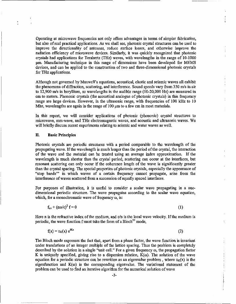
Operating at microwave frequencies not only offers advantages in terms of simpler fabrication,but also of real practical applications. As we shall see, photonic crystal structures can be used toimprove the directionality of antennas, reduce surface losses, and otherwise improve theradiation efficiency of microwave devices. Similarly, it was quickly recognized that photoniccrystals had applications for Terahertz (THz) waves, with wavelengths in the range of 10-1000gim. Manufacturing technique in this range of dimensions have been developed for MEMSdevices, and can be applied to the construction of two and three-dimensional photonic crystalsfor THz applications.
Although not governed by Maxwell's equations, acoustical, elastic and seismic waves all exhibitthe phenomena of diffraction, scattering, and interference. Sound speeds vary from 330 m/s in airto 12,900 m/s in beryllium, so wavelengths in the audible range (10-20,000 Hz) are measured incm to meters. Phononic crystals (the acoustical analogue of photonic crystals) in this frequencyrange are large devices. However, in the ultrasonic range, with frequencies of 100 kHz to 10Mhz, wavelengths are again in the range of 100 gtm to a few cm in most materials.
In this report, we will consider applications of photonic (phononic) crystal structures tomicrowave, mm-wave, and THz electromagnetic waves, and acoustic and ultrasonic waves. Wewill briefly discuss recent experiments relating to seismic and water waves as well.
II. Basic Principles
Photonic crystals are periodic structures with a period comparable to the wavelength of thepropagating wave. If the wavelength is much longer than the period of the crystal, the interactionof the wave and the material can be treated using an average index approximation. If thewavelength is much shorter than the crystal period, scattering can occur at the interfaces, butresonant scattering can only occur if the coherence length of the wave is significantly greaterthan the crystal spacing. The special properties of photonic crystals, especially the appearance of"stop bands"' in which waves of a certain frequency cannot propagate, arise from theinterference of waves scattered from a succession of equally spaced interfaces.
For purposes of illustration, it is useful to consider a scalar wave propagating in a one-dimensional periodic structure. The wave propagates according to the scalar wave equation,which, for a monochromatic wave of frequency co, is:
fxx + (nco/c) 2 f = 0 (1)
Here n is the refractive index of the medium, and c/n is the local wave velocity. If the medium isperiodic, the wave function f must take the form of a Blochl° mode,
f(x) = UK(X) e iKx (2)
The Bloch mode expresses the fact that, apart from a phase factor, the wave function is invariantunder translations of an integer multiple of the lattice spacing. Thus the problem is completelydescribed by the solution in a single "unit cell." For a given frequency co, the propagation factorK is uniquely specified, giving rise to a dispersion relation, K(O). The solution of the waveequation for a periodic structure can be rewritten as an eigenvalue problem, where uK(x) is theeigenfunction and K((o) is the corresponding eigenvalue. The variational statement of theproblem can be used to find an iterative algorithm for the numerical solution of wave
-3-
propagation problems in complex, multi-dimensional photonic crystal designs (See Appendix Dof the monograph on photonic crystals by Joannopoulos, Meade, and Winn"
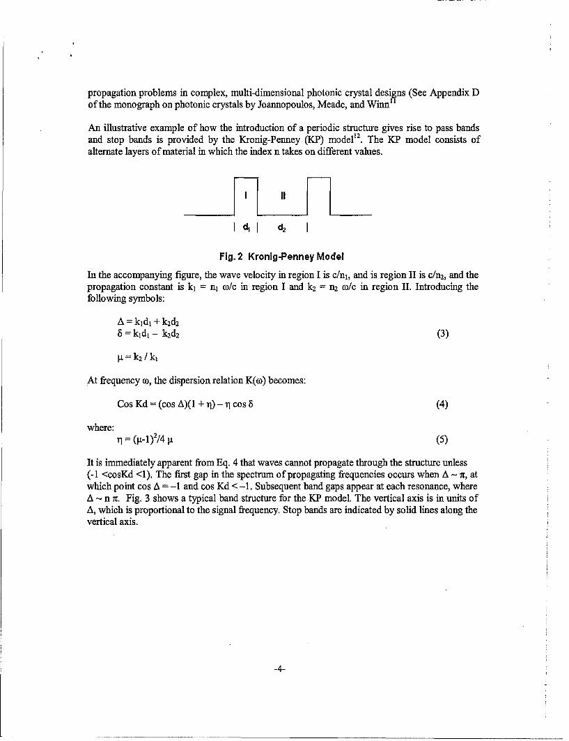
An illustrative example of how the introduction of a periodic structure gives rise to pass bandsand stop bands is provided by the Kronig-Penney (KP) model12. The KP model consists ofalternate layers of material in which the index n takes on different values.
I I
Id1 d2 I
Fig. 2 Kronig-Penney Model
In the accompanying figure, the wave velocity in region I is c/ni, and is region I1 is c/n 2, and thepropagation constant is ki = n, cr/c in region I and k2 = n2 (0/c in region II. Introducing thefollowing symbols:
A = kid, + k2 d28 =kid, - k2 d2 (3)
=k 2 / k,
At frequency (o, the dispersion relation K(o)) becomes:
Cos Kd = (cos A)(l + TI) -rl cos 8 (4)
where:T1 = (R--1) 2/4 jj (5)
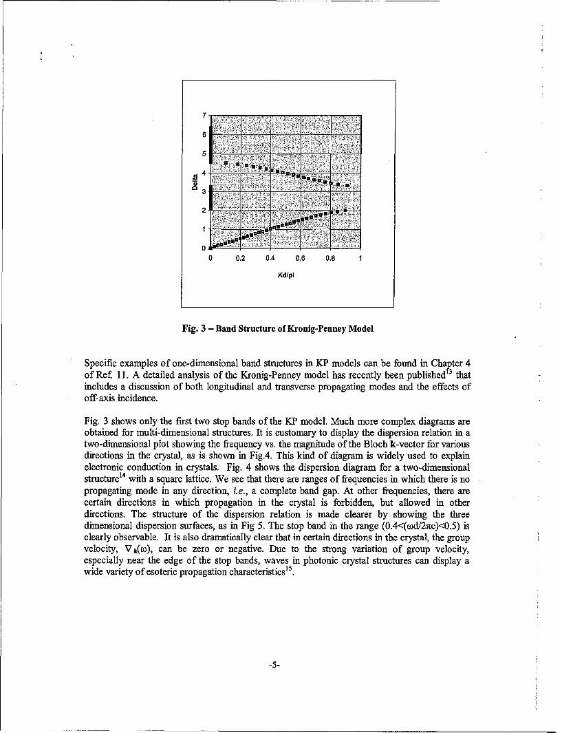
It is immediately apparent from Eq. 4 that waves cannot propagate through the structure unless(-1 <cosKd <1). The first gap in the spectrum of propagating frequencies occurs when A - a, atwhich point cos A = -1 and cos Kd < -1. Subsequent band gaps appear at each resonance, whereA - n 7r. Fig. 3 shows a typical band structure for the KP model. The vertical axis is in units ofA, which is proportional to the signal frequency. Stop bands are indicated by solid lines along thevertical axis.
-4-
5 ',, -6 .. :•, Y.',••I •ih i•!; V';.:
44
2
0 0.2 0.4 0.6 0.8 1
Kdlpl
Fig. 3 - Band Structure of Kronig-Penney Model
Specific examples of one-dimensional band structures in KP models can be found in Chapter 4of Ref 11. A detailed analysis of the Kronig-Penney model has recently been published thatincludes a discussion of both longitudinal and transverse propagating modes and the effects ofoff-axis incidence.
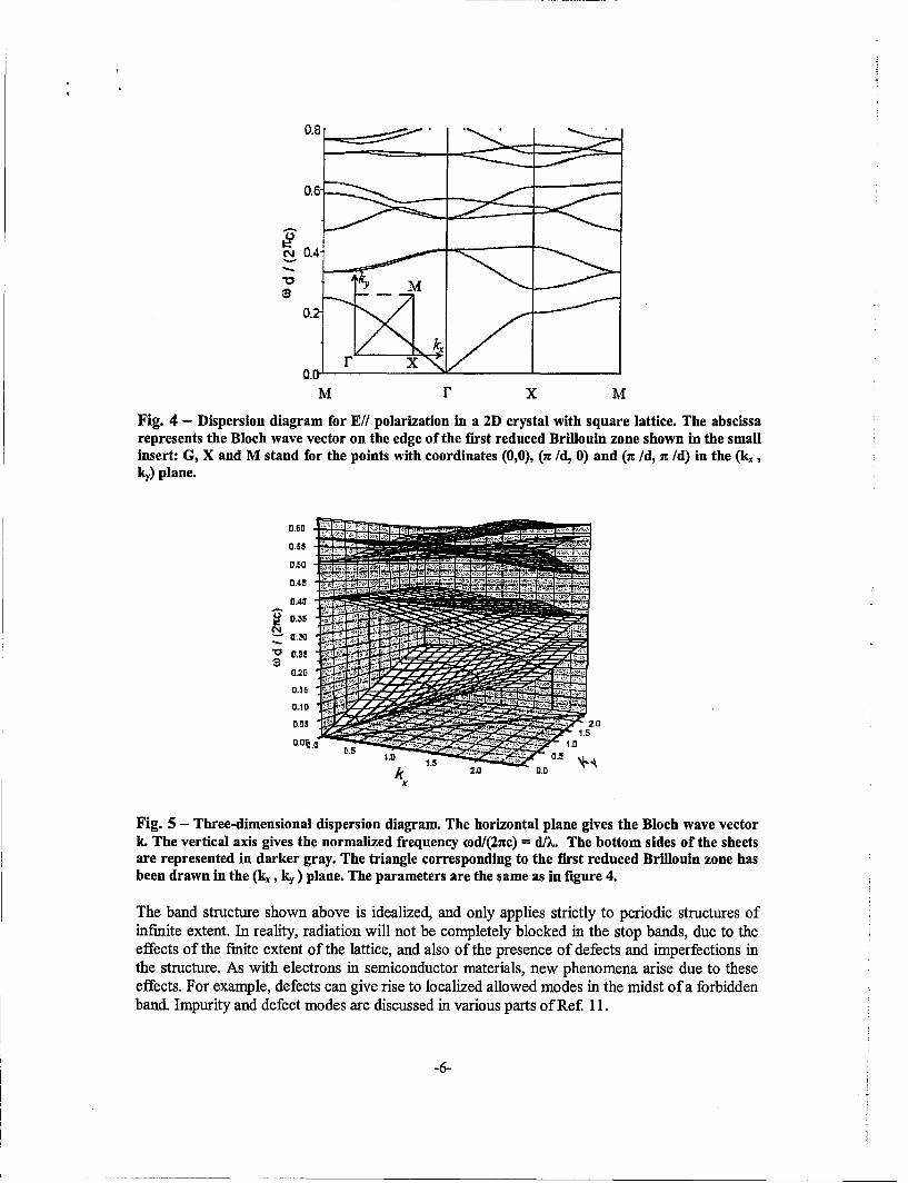
Fig. 3 shows only the first two stop bands of the KP model. Much more complex diagrams areobtained for multi-dimensional structures. It is customary to display the dispersion relation in atwo-dimensional plot showing the frequency vs. the magnitude of the Bloch k-vector for variousdirections in the crystal, as is shown in Fig.4. This kind of diagram is widely used to explainelectronic conduction in crystals. Fig. 4 shows the dispersion diagram for a two-dimensionalstructure14 with a square lattice. We see that there are ranges of frequencies in which there is nopropagating mode in any direction, i.e., a complete band gap. At other frequencies, there arecertain directions in which propagation in the crystal is forbidden, but allowed in otherdirections. The structure of the dispersion relation is made clearer by showing the threedimensional dispersion surfaces, as in Fig 5. The stop band in the range (0.4<(oxd/2I2c)<0.5) isclearly observable. It is also dramatically clear that in certain directions in the crystal, the groupvelocity, V k(0)), can be zero or negative. Due to the strong variation of group velocity,especially near the edge of the stop bands, waves in photonic crystal structures can display a15wide variety of esoteric propagation characteristics .
-5-
0.8
0.06
M r X M
Fig. 4 - Dispersion diagram for E// polarization in a 2D crystal with square lattice. The abscissarepresents the Bloch wave vector on the edge of the first reduced Brillouin zone shown in the smallinsert: G, X and M stand for the points with coordinates (0,0), (n Id, 0) and (a /d, U /d) in the (k,,ky) plane.
0.55
0.35
"0 ID
0.20:
0.15
0.1D -1
0.0t .0+" .
D.S 0.. 1.
k 2.0 0.
Fig. 5 - Three-dimensional dispersion diagram. The horizontal plane gives the Bloch wave vectork. The vertical axis gives the normalized frequency €od/(2-xc) = d/I. The bottom sides of the sheetsare represented in darker gray. The triangle corresponding to the first reduced Brillouin zone hasbeen drawn in the (k1 , ky ) plane. The parameters are the same as in figure 4.
The band structure shown above is idealized, and only applies strictly to periodic structures ofinfinite extent. In reality, radiation will not be completely blocked in the stop bands, due to theeffects of the finite extent of the lattice, and also of the presence of defects and imperfections inthe structure. As with electrons in semiconductor materials, new phenomena arise due to theseeffects. For example, defects can give rise to localized allowed modes in the midst of a forbiddenband. Impurity and defect modes are discussed in various parts of Ref 11.
-6-
In what follows, we will not go into detail concerning computational methods. Simply stated,there are two commonly used approaches to modeling photonic crystal structures. Both start withthe "Master Equation," which for electromagnetic problems is obtained from Maxwell'sequations as:
Curl [(curl H(r))/E(r)] = (co /c)2 H(r), (6)
where Maxwell's equations have been written in the frequency domain. For acoustics problems,the master equation is written:
X div [(grad P)/p] = -co2 p (7)
As in the Kronig-Penney model, we invoke the Bloch theorem, and look for solutions that areperiodic in space, with a periodicity given by the functional form, exp(ik.r). Then we seek thedispersion relation in the form co (k). The dispersion relation is an expression of the eigenvaluesof the master equation as k is varied over all directions in the crystal. To obtain the eigenvalues,the master equation is usually converted to a variational problem and solved by conventionalmatrix methods. The calculation is straightforward, but requires a large number of basisfunctions to obtain the band structure accurately.
The other approach is to view the master equation as a propagation problem in the time domain,and solve the initial condition problem for the geometry under investigation. This method ismore suited to analysis of finite structures and structures containing defects. The most commonmethod used to solve the propagation equation is the Finite Difference Time Domain (FTDT)method. A summary of various computational methods can be found in the book'6,Electromagnetic Applications of Photonic Band Gap Materials and Structures.
A general analysis of wave propagation in periodic structures has been carried out' 7 byEconomou and Sigalas, in Greece. They contrast the two possible topologies of band gapmaterials, a) Cermets, in which the scattering medium (low-velocity) is distributed in isolatedinclusions surrounded by the host medium (high-velocity), and b) Networks, in which thescattering medium inclusions are connected, and form a continuous network throughout the hostmaterial. The two topologies are analyzed for both the electromagnetic and acoustic masterequations. For acoustic (and elastic) waves, they find that the cermet topology is more favorablefor the formation of spectral gaps (stop bands), whereas for the electromagnetic case, thenetwork topology is more favorable. They offer general rules relating the fractional bandwidth ofand the upper frequency of the first stop band to the fill factor and velocity ratio of the twomedia.
If. Microwave Applications
Because of the difficulties in fabricating photonic crystal structures at the scale of an opticalwavelength, much of the experimental work has been done using microwaves. At microwavefrequencies (3-300 GHz) wavelengths are measured in cm or nmm, so conventional machiningtechniques can be used to fabricate components. Dielectric materials exhibit high refractiveindices at these frequencies, and additionally, metallic components can be used, adding anotherdimension to the design space. In addition, structure can be added to the individual elements of a
-7-
photonic crystal array, so that each component of the array becomes a circuit element, with anadjustable capacitance and inductance.
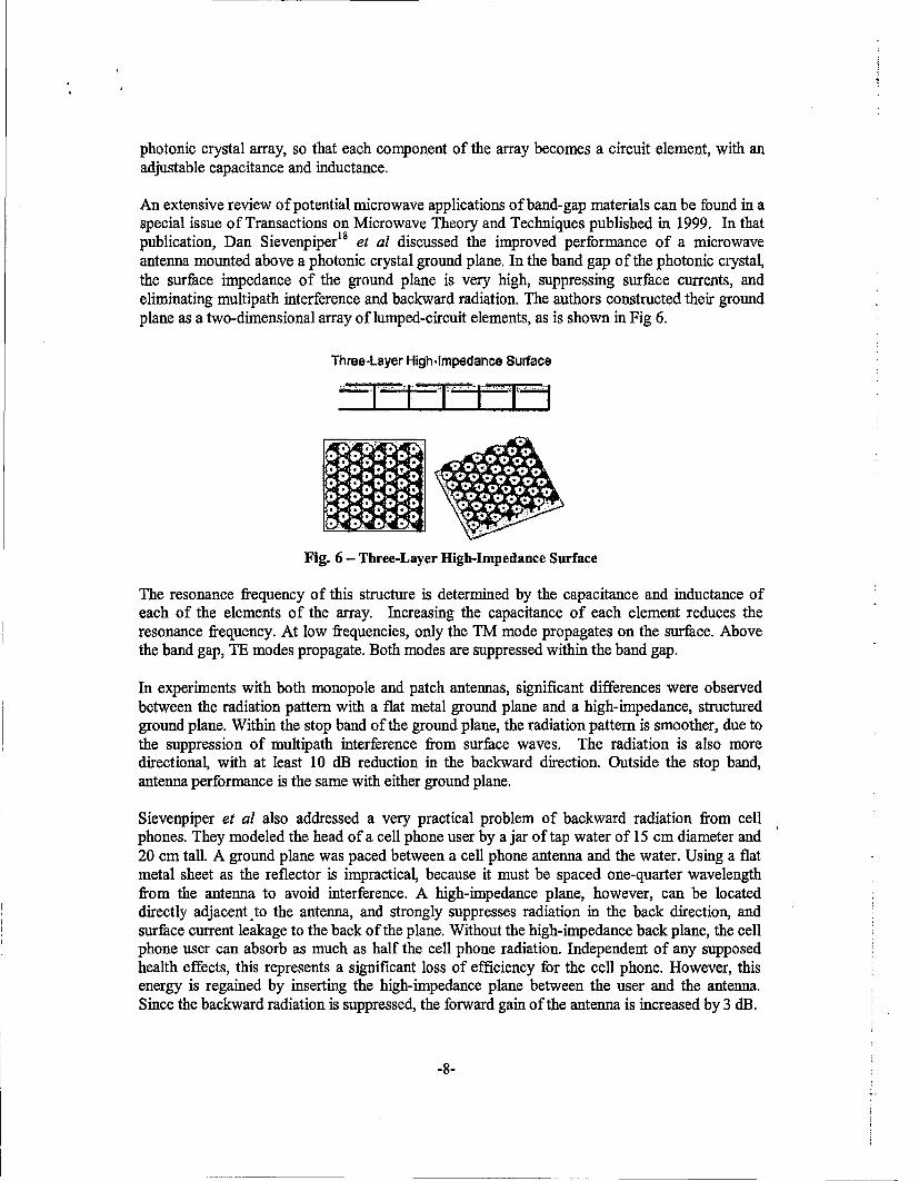
An extensive review of potential microwave applications of band-gap materials can be found in aspecial issue of Transactions on Microwave Theory and Techniques published in 1999. In thatpublication, Dan Sievenpiper18 et al discussed the improved performance of a microwaveantenna mounted above a photonic crystal ground plane. In the band gap of the photonic crystal,the surface impedance of the ground plane is very high, suppressing surface currents, andeliminating multipath interference and backward radiation. The authors constructed their groundplane as a two-dimensional array of lumped-circuit elements, as is shown in Fig 6.
Three-Layer Highb.Impedance Surface
Fig. 6 - Three-Layer High-Impedance Surface
The resonance frequency of this structure is determined by the capacitance and inductance ofeach of the elements of the array. Increasing the capacitance of each element reduces theresonance frequency. At low frequencies, only the TM mode propagates on the surface. Abovethe band gap, TE modes propagate. Both modes are suppressed within the band gap.
In experiments with both monopole and patch antennas, significant differences were observedbetween the radiation pattern with a flat metal ground plane and a high-impedance, structuredground plane. Within the stop band of the ground plane, the radiation pattern is smoother, due tothe suppression of multipath interference from surface waves. The radiation is also moredirectional, with at least 10 dB reduction in the backward direction. Outside the stop band,antenna performance is the same with either ground plane.
Sievenpiper et al also addressed a very practical problem of backward radiation from cellphones. They modeled the head of a cell phone user by a jar of tap water of 15 cm diameter and20 cm tall. A ground plane was paced between a cell phone antenna and the water. Using a flatmetal sheet as the reflector is impractical, because it must be spaced one-quarter wavelengthfrom the antenna to avoid interference. A high-impedance plane, however, can be locateddirectly adjacent to the antenna, and strongly suppresses radiation in the back direction, andsurface current leakage to the back of the plane. Without the high-impedance back plane, the cellphone user can absorb as much as half the cell phone radiation. Independent of any supposedhealth effects, this represents a significant loss of efficiency for the cell phone. However, thisenergy is regained by inserting the high-impedance plane between the user and the antenna.Since the backward radiation is suppressed, the forward gain of the antenna is increased by 3 dB.
-8-
Cell phone manufacturers have not adopted the practice of using a high-impedance back plane toshield cell phone users, however 19. Apparently, they concluded that it would add an unacceptableamount to the cost and size of cell phones.
Several other authors have explored the use of high-Z surfaces to improve antennaperformance 20' 21. As the authors of Ref 19 point out, "The microstrip patch antenna is a verypopular design, because of its low profile, it can be non-planar, is easy to manufacture, and isinexpensive and robust." Patch antenna performance, however, is limited by surface wave lossesand interference. The use of a band-gap material to create a high-impedance back plane allowsthe antenna to be placed directly on the back plane, to make a more compact package.Suppression of the surface current leads to a more directional radiation pattern, and suppressionof side lobes due to interference.
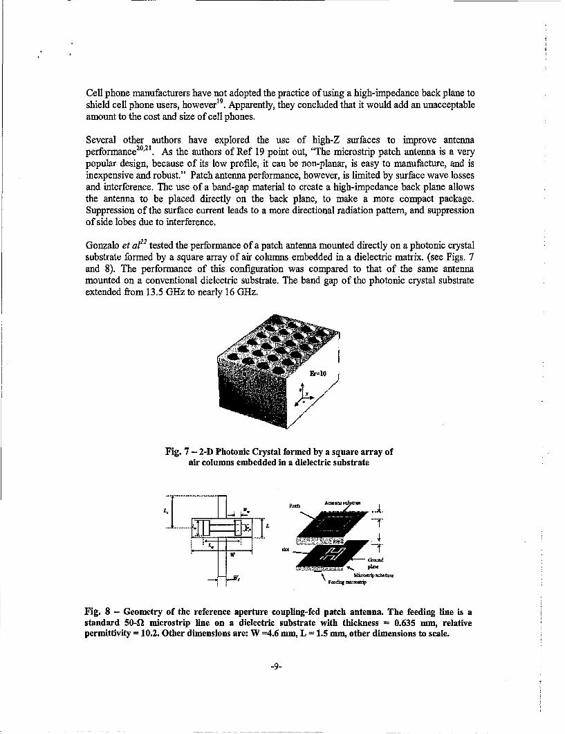
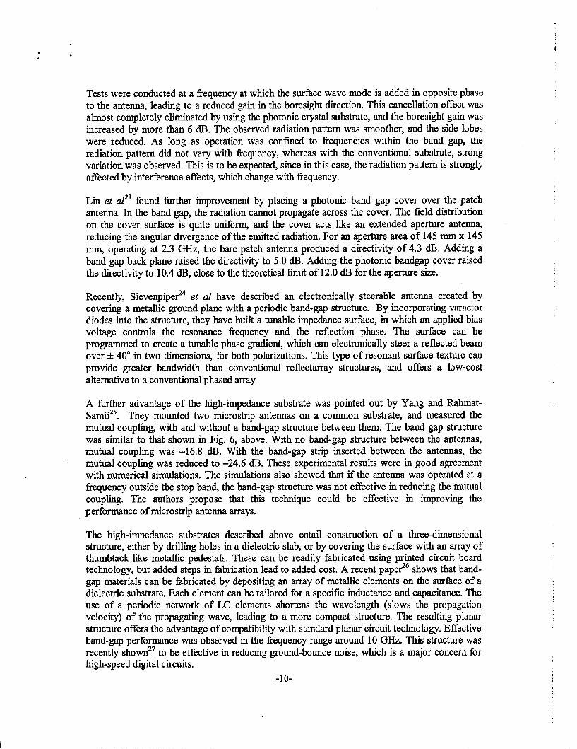
Gonzalo et at22 tested the performance of a patch antenna mounted directly on a photonic crystalsubstrate formed by a square array of air columns embedded in a dielectric matrix. (see Figs. 7and 8). The performance of this configuration was compared to that of the same antennamounted on a conventional dielectric substrate. The band gap of the photonic crystal substrateextended from 13.5 GI-z to nearly 16 GHz.
S Er=1/
Fig. 7 - 2-D Photonic Crystal formed by a square array ofair columns embedded in a dielectric substrate
"-•"•' -••
Fig. 8 - Geometry of the reference aperture coupling-fed patch antenna. The feeding line is astandard 50-4 microstrip line on a dielectric substrate with thickness = 0.635 mm, relativepermittivity = 10.2. Other dimensions are: W -4.6 mm, L = 1.5 mm, other dimensions to scale.
-9-
Tests were conducted at a frequency at which the surface wave mode is added in opposite phaseto the antenna, leading to a reduced gain in the boresight direction. This cancellation effect wasalmost completely eliminated by using the photonic crystal substrate, and the boresight gain wasincreased by more than 6 dB. The observed radiation pattern was smoother, and the side lobeswere reduced. As long as operation was confined to frequencies within the band gap, theradiation pattern did not vary with frequency, whereas with the conventional substrate, strongvariation was observed. This is to be expected, since in this case, the radiation pattern is stronglyaffected by interference effects, which change with frequency.
Lin et al23 found further improvement by placing a photonic band gap cover over the patchantenna. In the band gap, the radiation cannot propagate across the cover. The field distributionon the cover surface is quite uniform, and the cover acts like an extended aperture antenna,reducing the angular divergence of the emitted radiation. For an aperture area of 145 mm x 145mm, operating at 2.3 GHz, the bare patch antenna produced a directivity of 4.3 dB. Adding aband-gap back plane raised the directivity to 5.0 dB. Adding the photonic bandgap cover raisedthe directivity to 10.4 dB, close to the theoretical limit of 12.0 dB for the aperture size.
Recently, Sievenpiper2 4 et al have described an electronically steerable antenna created bycovering a metallic ground plane with a periodic band-gap structure. By incorporating varactordiodes into the structure, they have built a tunable impedance surface, in which an applied biasvoltage controls the resonance frequency and the reflection phase. The surface can beprogrammed to create a tunable phase gradient, which can electronically steer a reflected beamover + 400 in two dimensions, for both polarizations. This type of resonant surface texture canprovide greater bandwidth than conventional reflectarray structures, and offers a low-costalternative to a conventional phased array
A further advantage of the high-impedance substrate was pointed out by Yang and Rahmat-Samii25. They mounted two microstrip antennas on a common substrate, and measured themutual coupling, with and without a band-gap structure between them. The band gap structurewas similar to that shown in Fig. 6, above. With no band-gap structure between the antennas,mutual coupling was -16.8 dB. With the band-gap strip inserted between the antennas, themutual coupling was reduced to -24.6 dB. These experimental results were in good agreementwith numerical simulations. The simulations also showed that if the antenna was operated at afrequency outside the stop band, the band-gap structure was not effective in reducing the mutualcoupling. The authors propose that this technique could be effective in improving theperformance of microstrip antenna arrays.
The high-impedance substrates described above entail construction of a three-dimensionalstructure, either by drilling holes in a dielectric slab, or by covering the surface with an array ofthumbtack-like metallic pedestals. These can be readily fabricated using printed circuit boardtechnology, but added steps in fabrication lead to added cost. A recent paper26 shows that band-gap materials can be fabricated by depositing an array of metallic elements on the surface of adielectric substrate. Each element can be tailored for a specific inductance and capacitance. Theuse of a periodic network of LC elements shortens the wavelength (slows the propagationvelocity) of the propagating wave, leading to a more compact structure. The resulting planarstructure offers the advantage of compatibility with standard planar circuit technology. Effectiveband-gap performance was observed in the frequency range around 10 GHz. This structure wasrecently shown27 to be effective in reducing ground-bounce noise, which is a major concern forhigh-speed digital circuits.
-10-
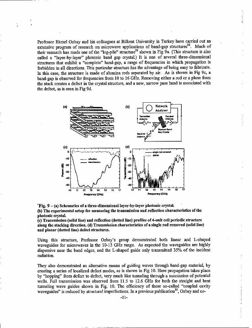
Professor Ekmel Ozbay and his colleagues at Bilkent University in Turkey have carried out anextensive program of research on microwave applications of band-gap structures28. Much oftheir research has made use of the "log-pile" structure29 shown in Fig 9a. (This structure is alsocalled a "layer-by-layer" photonic band gap crystal.) It is one of several three-dimensionalstructures that exhibit a "complete" band-gap, a range of frequencies in which propagation isforbidden in all directions. This particular structure has the advantage of being easy to fabricate.In this case, the structure is made of alumina rods separated by air. As is shown in Fig 9c, aband-gap is observed for frequencies from 10 to 16 GHz. Removing either a rod or a plane fromthe stack creates a defect in the crystal structure, and a new, narrow pass band is associated withthe defect, as is seen in Fig 9d.
(a) (bl) Q Niawark
(C) (d)-
0.i............ ... 0 Si, . a a-10 . .. ... .. .M d - --10
-30 3
-50 -60,
IC 11 t 12 IA 14 5 16 17 10 Ii 12 IS 14 16 1$ 17
Pt1Queny(OIHZ) PIqe-MNUf~~IZ)
'Fig. 9 -(a) Schematics of a three-dimensional layer-by-layer photonic crystal.(b) The experimental setup for measuring the transmission and reflection characteristics of thephotonic crystal.(c) Transmission (solid line) and reflection (dotted line) profiles of 4-unit cell periodic structurealong the stacking direction. (d) Transmission characteristics of a single rod removed (solid line)and planar (dotted line) defect structures.
Using this structure, Professor Ozbay's group demonstrated both linear and L-shapedwaveguides for microwaves in the 10-13 GI~z range. As expected the waveguides are highlydispersive near the band edges, and the L-shaped guide only transmitted 35% of the incidentradiation.
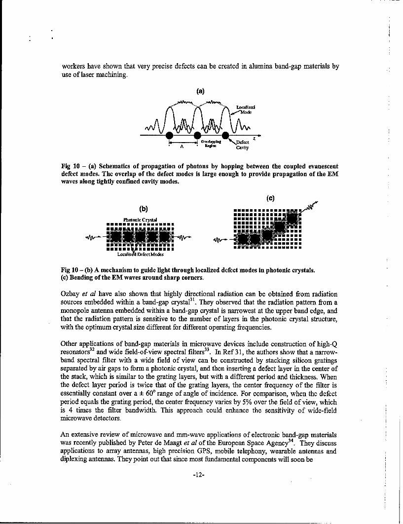
They also demonstrated an alternative means of guiding waves through band-gap material, bycreating a series of localized defect modes, as is shown in Fig 10. Here propagation takes placeby "hopping" from defect to defect, very much like tunneling through a succession of potentialwells. Full transmission was observed from 11.5 to 12.6 GHz for both the straight and benttunneling wave guides shown in Fig. 10. The efficiency of these so-called "coupled cavitywaveguides" is reduced by structural imperfections. In a previous publication30 , Ozbay and co-
-11-
workers have shown that very precise defects can be created in alumina band-gap materials by
use of laser machining.
(a)
1ncalizcd
A 1II Cavity
Fig 10 - (a) Schematics of propagation of photons by hopping between the coupled evanescentdefect modes. The overlap of the defect modes is large enough to provide propagation of the EMwaves along tightly confined cavity modes.
(C)(b) mumm===n=sllllo__
ihotanffe CrystalEKiiEEii Em...
•nu'iuc:; uw m.i ..Uuunil• l~~~ niunuu
Localim¢d Dcfct Mods
Fig 10 - (b) A mechanism to guide light through localized defect modes in photonic crystals.(c) Bending of the EM waves around sharp corners.
Ozbay et al have also shown that highly directional radiation can be obtained from radiationsources embedded within a band-gap crystal31. They observed that the radiation pattern from amonopole antenna embedded within a band-gap crystal is narrowest at the upper band edge, andthat the radiation pattern is sensitive to the number of layers in the photonic crystal structure,with the optimum crystal size different for different operating frequencies.
Other applications of band-gap materials in microwave devices include construction of high-Qresonators32 and wide field-of-view spectral filters33. In Ref 31, the authors show that a narrow-band spectral filter with a wide field of view can be constructed by stacking silicon gratingsseparated by air gaps to form a photonic crystal, and then inserting a defect layer in the center ofthe stack, which is similar to the grating layers, but with a different period and thickness. Whenthe defect layer period is twice that of the grating layers, the center frequency of the filter isessentially constant over a ± 600 range of angle of incidence. For comparison, when the defectperiod equals the grating period, the center frequency varies by 5% over the field of view, whichis 4 times the filter bandwidth. This approach could enhance the sensitivity of wide-fieldmicrowave detectors.
An extensive review of microwave and mm-wave applications of electronic band-gap materialswas recently published by Peter de Maagt et al of the European Space Agency 34 . They discussapplications to array antennas, high precision GPS, mobile telephony, wearable antennas anddiplexing antennas. They point out that since most fundamental components will soon be
-12-

available using band-gap technology, "a fully integrated receiver could be developed ... and trueintegration of active and passive band-gap components can now begin to materialize." Of theseveral important applications for band gap structures that have been identified anddemonstrated, the one nearest to practical use is for conformal antennas, making use of a high-impedance ground plane. Other variants on antenna design attractive for near-term applicationare highly steerable antennas and antennas embedded in clothing 35. Fabrication of microwaveband-gap structures is attractively simple, and the capacitance and inductance of individualelements can be tailored easily. Band-gap structures are compatible with millimeter waveintegrated circuits.
IV. Terahertz Applications
The term, Terahertz Radiation, refers to the portion of the electromagnetic spectrum between300 GHz and 3 THz36 (100-1000 prn). This region of the spectrum has not been exploited untilrecently, mainly because of strong water absorption over much of the frequency range, and alack of suitable sources and detectors. There has been some scientific interest in THzspectroscopy, however. Most simple molecules have strong rotational absorption lines in thisregion. It is also a region of great interest to astronomers, since the radiation from interstellardust is well approximated by a 30 K black body spectrum, which peaks at about 100 itm.Currently, THz devices are under investigation for medical imaging applications, although theapplications are limited by the prevalence of water in tissue. The primary applications are indentistry and dermatology .
The scale length of Terahertz devices simplifies the problems of fabrication and assembly forphotonic crystal structures. Devices can be assembled using well-developed MEMS techniques,and can be compact and highly integrated.. Many of the applications considered parallel those inthe microwave region, including improving the directionality of antennas, both in transmissionand in imaging arrays. DeMaagt et al38 report on the improved directionality of a dipole antennaoperating at 500 GHz when mounted on a "woodpile" photonic crystal with a 3-dimensionalbandgap extending from 480-540 GHz.. They measured improvement from 2 dB directivity foran air-suspended dipole to 11 dB for the same dipole backed with a photonic crystal. The entiredevice was approximately six mm2 in area. The ultimate objective is to assemble such devicesinto an imaging array.
A recent Japanese paper 39 describes a different way in which photonic crystals can enhance theprocess of THz generation. A common method of generating TI-Iz radiation is by beating twosingle-mode lasers operating with a THz difference frequency on a photoconductive antenna4.The Japanese group embedded the photoconducting antenna between two photonic crystalstructures. The embedded antenna achieved a peak emission intensity of more than twice that ofa bare antenna. Strong enhancement was observed near the band edge of the photonic crystal,due to the high density of states at that frequency.
As in the microwave range, metallic elements can be used with THz devices. A Scottish researchgroup41 has developed a tunable metallic photonic crystal filter for THz applications that consistsof an array of movable metallic grids. Tuning is achieved by moving alternate grids sideways,changing the transverse periodicity of the array. This research is also interesting because itdemonstrates some of the manufacturing techniques that can be employed in the THz and mm-wave regime. The first prototype42 of this filter was fabricated from sheets of aluminum alloymachined to a thickness of 500 Rim. The cross-sectional area of the filter, including mechanical
-13-

supports, was 60mm x 40mm, with a transverse grid spacing of 1.8 mm. This device was testedat 70-110 GHz (mm-wave), and demonstrated tunability of the pass-band over a range of 3.5GHz, with an insertion loss of 1.1-1.7 dB.
The authors then fabricated and tested a similar device, but manufactured from gold-coatedsilicon, using conventional MEMS techniques. Since the skin depth of gold at the operatingfrequency (70-150 GHz) is about 0.25 pm, a coating thickness of 1.2 grm was sufficient. Thisdevice showed tunability over a range of 7 GI-z, with an insertion loss of 1 dB or less over theoperating range. The authors comment that the use of MEMS fabrication techniques allow theconstruction of devices operating at higher frequencies (1-5 TI-z), where conventionalmachining techniques cannot be used. Their work also demonstrates the value of prototyping atlower frequencies.
A group at Tohuko University has recently demonstrated a novel method of fabricating photoniccrystals for THz applications 43. They fabricated 300 jim-diameter copper spheres, and packedthem into an fcc structure on a graphite base. The spheres were lightly sintered to form "necks"between adjacent spheres, constructing a three-dimensional template for an inverse photoniccrystal. The interstitial spaces in the template were filled with a dielectric epoxy resin. After theresin was cured, the copper spheres were etched away, leaving a regular array of air holes in theepoxy matrix. The resulting structure exhibited a 160-GHz-wide stop band around 500 GHz inthe [ 111 ] direction.
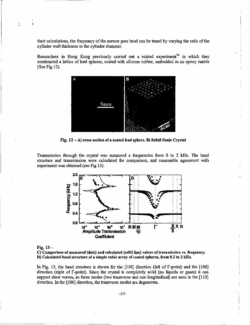
AFOSR has sponsored research on integrated optics for TI-z devices, especially at the highfrequency end of the THz range. A group at the University of Delaware has demonstrated the useof a planar photonic crystal waveguide to create a compact integrated optics device operating at30 THz (10 jim) 44. A waveguide was created by leaving a solid stripe through the center of atwo-dimensional photonic crystal., as is shown in Fig. 11. Transmission was tested using a CO2laser operating at frequencies from 10.1 gtm to 10.7 Wim (28.0 - 29.7 jim)., and was also modeledusing a 3D-Finite-Difference-Time-Domain (FDTD) method4 5. Both the measured andcalculated transmission are shown in Fig 12. The scatter in the experimental data is attributedpartly to imperfections in the fabrication process, and partly to possible variations in the insertionloss as the input laser is tuned from line to line. The gap in data from 28.6 to 29.0 THz is due tothe unavailability of laser lines at those frequencies.
-14-
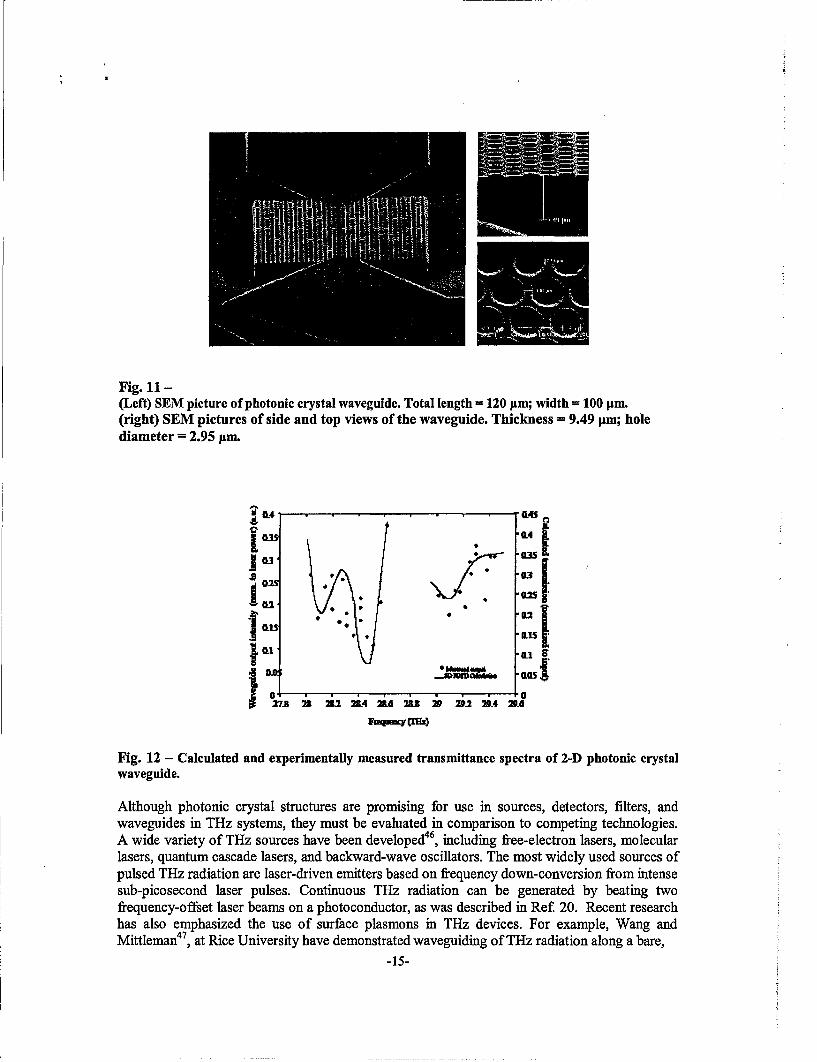
Fig. 11-(Left) SEM picture of photonic crystal waveguide. Total length f 120 Pm; width = 100 pm.(right) SEM pictures of side and top views of the waveguide. Thickness = 9.49 prm; holediameter = 2.95 pm.
S0.4. 0.43
l:0351W 0.L
025
FL IS0.0.15
27Bit 2i, 32i34 2id 213 2a 2D.2 29.4 29.8
Fig. 12 - Calculated and experimentally measured transmittance spectra of 2-D photonic crystalwaveguide.
Although photonic crystal structures are promising for use in sources, detectors, filters, andwaveguides in THz systems, they must be evaluated in comparison to competing technologies.A wide variety of THz sources have been developed46, including free-electron lasers, molecularlasers, quantum cascade lasers, and backward-wave oscillators. The most widely used sources ofpulsed THz radiation are laser-driven emitters based on frequency down-conversion from intensesub-picosecond laser pulses. Continuous THz radiation can be generated by beating twofrequency-offset laser beams on a photoconductor, as was described in Ref. 20. Recent researchhas also emphasized the use of surface plasmons in THz devices. For example, Wang andMittlemannT, at Rice University have demonstrated waveguiding of THz radiation along a bare,
-15-

stainless-steel wire with low attenuation and negligible group velocity dispersion.Metamaterials 48 comprising discrete circuit elements also hold out great promise for applicationin the THz frequency range, and may suffer less from significant group dispoersion effects thanthose composed of photonic crystal structures.
Terahertz radiation represents a new area of physics and engineering research. Unlike themicrowave regime, an extensive body of techmology does not already exist for THz use, so newapproaches and devices do not face the same barriers to entry. The physical scale of photoniccrystal structures in the THz'range is commensurate with the use of established MEMSfabrication techniques. It is very likely that in certain applications, especially those in whichbroad bandwidth is not required, photonic crystal devices will find significant specializedapplications for THz devices. In 2002, the European Space Agency (ESA) launched a multi-laboratory project called "Star Tiger" to develop Thz imaging technology based on the use ofphotonic crystal mirrors. The project successfully produced a prototype imaging system on achip 49. The THz waves were detected by heterodyning the signal down to radio frequencies, dueto the lack of direct detectors. ESA has continued research on THz applications of band-gapmaterials, and is currently developing THz imaging arrays50 .
IV. Elastic, Acoustic and Ultrasonic Applications
Shortly after the publication of the first few papers on Photonic Crystals (Ref. 6,7), researchbegan on applying band-gap structures to acoustic and elastic waves 51. The literature on theseapplications is nowhere as extensive as on photonic applications, and much of the research iscarried out outside the US, with active groups in Spain, France, Taiwan, Hong Kong, Greece,South Korea and Canada. Acoustical experiments do not require as sophisticated methods ormaterials as microwave or optical experiments. A Spanish research group52 constructed a"phononic crystal" by hanging an array of aluminum cylinders from a rotating support, anddriving a speaker with a frequency generator and observing the transmission with conventionalmicrophones. Experiments were conducted at audio frequencies (250-3500 Hz) and attenuationand phase delay were observed. Several configurations were examined, with rod diametersvarying from 1 to 4 cm, and lattice spacings of 5.5 and 11 cm. in square and hexagonal lattices.The experimental results showed the expected agreement with theory, with strong attenuationwithin the band gap (although the data was quite noisy) and anomalous dispersion at the bandedges. In addition, the authors observed "deaf bands," which were regions of frequency wheresound in certain directions was trapped inside the structure for reasons of symmetry.
As in the microwave regime, the design space for elastic band gap structures is very large, withseveral parameters that can be chosen to determine the structure's response. Whether in two orthree dimensions, the location and extent of the stop bands depends on the dimensions, soundspeeds and densities of the materials used, and the internal structure of the lattice components.Thus, in an array of cylinders, the cylinders can be solid or have a hollow core, which can befilled with a separate material, or the outside of the cylinder can be coated with a disparatematerial. Khelif et a153 modeled a two-dimensional band gap structure of steel cylinders in water,and calculated the transmission properties of this lattice, comparing results with solid cylindersto those from hollow cylinders of various wall thickness. With solid cylinders, the band gapextended from 100 kf-z to 200 kHz. With hollow cylinders, the upper band edge was extended to220 kHz, and a narrow pass band was introduced within the band gap, due to a resonance withinthe cylinders that interferes with the wave cancellations within the entire lattice. According to
-16-
their calculations, the frequency of the narrow pass band can be tuned by varying the ratio of thecylinder wall thickness to the cylinder diameter.
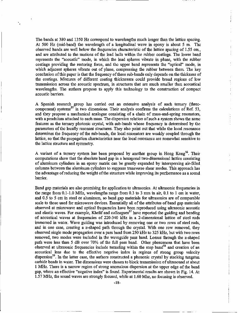
Researchers in Hong Kong previously carried out a related experiment54 in which theyconstructed a lattice of lead spheres, coated with silicone rubber, embedded in an epoxy matrix(See Fig. 12).
Fig. 12 - A) cross section of a coated lead sphere. B) 8x8x8 Sonic Crystal
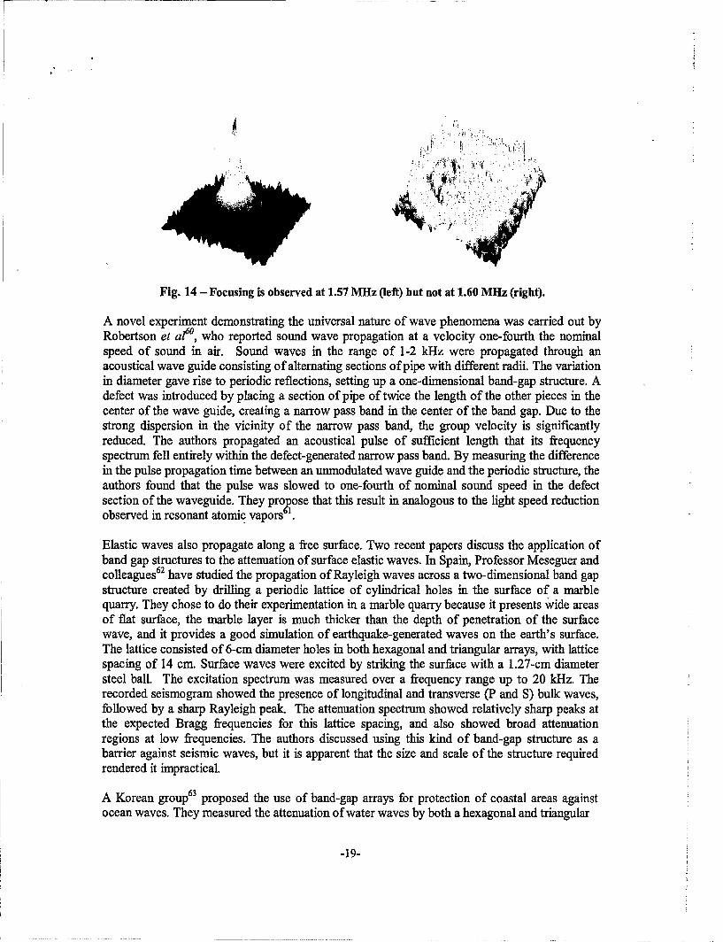
Transmission through the crystal was measured a frequencies from 0 to 2 kHz. The bandstructure and transmission were calculated for comparison, and reasonable agreement withexperiment was obtained (see Fig 13).
2.0 "CD
0.0
0.8
0. • 10.a 1W 1W"' RMM ] XXRAmplitude Transmission 10 5
Coeff'dent
Fig. 13-C) Comparison of measured (dots) and calculated (solid line) values of transmission vs. frequency.D) Calculated band structure of a simple cubic array of coated spheres, from 0.2 to 2 kHz.
In Fig. 13, the band structure is shown for the [110] direction (left of F-point) and the [100]direction (right of F-point). Since the crystal is completely solid (no liquids or gases) it cansupport shear waves, so three modes (two transverse and one longitudinal) are seen in the [110]direction. In the [100] direction, the transverse modes are degenerate.
-17-
The bands at 380 and 1350 Hz correspond to wavelengths much longer than the lattice spacing.At 500 Hz (mid-band) the wavelength of a longitudinal wave in epoxy is about 5 m. Theobserved bands are well below the frequencies characteristic of the lattice spacing of 1.55 cm.,and are attributed to the motions of the lead balls within the rubber coatings. The lower bandrepresents the "acoustic" mode, in which the lead spheres vibrate in phase, with the rubbercoatings providing the restoring force, and the upper band represents the "optical" mode, inwhich adjacent spheres vibrate out of phase, compressing the rubber between them. The keyconclusion of this paper is that the frequency of these sub-bands only depends on the thickness ofthe coatings. Mixtures of different coating thicknesses could provide broad regions of lowtransmission across the acoustic spectrum, in structures that are much smaller than acousticalwavelengths. The authors propose to apply this technology to the construction of compactacoustic barriers.
A Spanish research group has carried out an extensive analysis of such ternary (three-component) systems55 in two dimensions. Their analysis confirms the calculations of Ref 53,and they propose a mechanical analogue consisting of a chain of mass-and-spring resonators,with a pendulum attached to each mass. The dispersion relation of such a system shows the samefeatures as the ternary photonic crystal, with sub-bands whose frequency is determined by theparameters of the locally resonant structures. They also point out that while the local resonancedetermines the frequency of the sub-bands, the local resonators are weakly coupled through thelattice, so that the propagation characteristics near the local resonance are somewhat sensitive tothe lattice structure and symmetry.
A variant of a ternary system has been proposed by another group in Hong Kong56. Theircomputations show that the absolute band gap in a hexagonal two-dimensional lattice consistingof aluminum cylinders in an epoxy matrix can be greatly expanded by interspersing air-filledcolumns between the aluminum cylinders to suppress transverse shear modes. This approach hasthe advantage of reducing the weight of the structure while improving its performance as a soundbarrier.
Band gap materials are also promising for application to ultrasonics. At ultrasonic frequencies inthe range from 0.1-1.0 MHz, wavelengths range from 0.3 to 3 mmn in air, 0.1 to 1 cm in water,and 0.5 to 5 cm in steel or aluminum, so band gap materials for ultrasonics are of comparablescale to those used for microwave devices. Essentially all of the attributes of band gap materialsobserved at microwave and optical frequencies have been reproduced using ultrasonic acousticand elastic waves. For example, Khelif and colleagues57 have reported the guiding and bendingof acoustical waves at frequencies of 220-340 kHz in a 2-dimensional lattice of steel rodsimmersed in water. Wave guiding was introduced by removing one or two rows of steel rods,and in one case, creating a z-shaped path through the crystal. With one row removed, theyobserved single mode propagation over a pass band from 250 kHz to 325 kHz, but with two rowsremoved, two modes were included in the waveguide pass band. Losses through the z-shapedpath were less than 5 dB over 70% of the full pass band. Other phenomena that have beenobserved at ultrasonic frequencies include tunneling within the stop band58 and creation of anacoustical lens due to the effective negative index in regions of strong group velocitydispersion". In the latter case, the authors constructed a phononic crystal by stacking tungstencarbide beads in water. The dimensions were chosen to block transmission of ultrasound at about1 MHz. There is a narrow region of strong anomalous dispersion at the upper edge of the bandgap, where an effective "negative index" is found. Experimental results are shown in Fig. 14. At1.57 MHz, the sound waves are strongly focused, while at 1.60 Mhz, no focusing is observed.
-18-
SI,
Fig. 14 - Focusing is observed at 1.57 MHz (left) but not at 1.60 MHz (right).
A novel experiment demonstrating the universal nature of wave phenomena was carried out byRobertson et a?6 , who reported sound wave propagation at a velocity one-fourth the nominalspeed of sound in air. Sound waves in the range of 1-2 kHz were propagated through anacoustical wave guide consisting of alternating sections of pipe with different radii. The variationin diameter gave rise to periodic reflections, setting up a one-dimensional band-gap structure. Adefect was introduced by placing a section of pipe of twice the length of the other pieces in thecenter of the wave guide, creating a narrow pass band in the center of the band gap. Due to thestrong dispersion in the vicinity of the narrow pass band, the group velocity is significantlyreduced. The authors propagated an acoustical pulse of sufficient length that its frequencyspectrum fell entirely within the defect-generated narrow pass band. By measuring the differencein the pulse propagation time between an unmodulated wave guide and the periodic structure, theauthors found that the pulse was slowed to one-fourth of nominal sound speed in the defectsection of the waveguide. They propose that this result in analogous to the light speed reductionobserved in resonant atomic vapors
Elastic waves also propagate along a free surface. Two recent papers discuss the application ofband gap structures to the attenuation of surface elastic waves. In Spain, Professor Meseguer andcolleagues 62 have studied the propagation of Rayleigh waves across a two-dimensional band gapstructure created by drilling a periodic lattice of cylindrical holes in the surface of a marblequarry. They chose to do their experimentation in a marble quarry because it presents wide areasof flat surface, the marble layer is much thicker than the depth of penetration of the surfacewave, and it provides a good simulation of earthquake-generated waves on the earth's surface.The lattice consisted of 6-cm diameter holes in both hexagonal and triangular arrays, with latticespacing of 14 cm. Surface waves were excited by striking the surface with a 1.27-cm diametersteel ball. The excitation spectrum was measured over a frequency range up to 20 kHz. Therecorded seismogram showed the presence of longitudinal and transverse (P and S) bulk waves,followed by a sharp Rayleigh peak. The attenuation spectrum showed relatively sharp peaks atthe expected Bragg frequencies for this lattice spacing, and also showed broad attenuationregions at low frequencies. The authors discussed using this kind of band-gap structure as abarrier against seismic waves, but it is apparent that the size and scale of the structure requiredrendered it impractical.
A Korean group63 proposed the use of band-gap arrays for protection of coastal areas againstocean waves. They measured the attenuation of water waves by both a hexagonal and triangular
-19-
2-dimensional lattice, at frequencies up to 10 Hz. 20 to 30 dB attenuation was observed overmuch of the frequency range, although the authors say that a more extensive array would lead tohigher attenuation. They propose that a hexagonal lattice with a spacing of 10m would provideprotection against most coastal water waves, and would be more eco-friendly than massive solidbarriers.
Band-gap structures have many positive attributes for application to acoustic and elastic waves.Readily available materials provide a wide range of parameters, especially mass density andsound speed. Thus, "high contrast" materials can be used to make compact structures. The scalelength of acoustic and elastic wave devices is convenient for fabrication, especially for ternarystructures, which offer real advantages for extending the stop bands and inserting narrow passbands. The use of fluid materials can effectively eliminate shear waves, simplifying thestructures.
At acoustical frequencies, the use of band gap materials for noise barriers has been extensivelystudied. Ternary systems offer some possibilities of providing high attenuation at lowfrequencies, while keeping the barrier at a reasonable size. However, conventional sound-absorbing materials are very effective, and it will be difficult to displace them for mostapplications. As in the microwave regime, band-gap materials are proposed for use in ultrasonicsystems as filters, wave guides, add-drop multiplexers, lenses, and components in detectors andtransmitters. At ultrasonic frequencies, band-gap structures may be the preferred approach forsome applications, especially those in which frequency selectivity is required.
V. Summary and Conclusions
Research on band-gap materials has been active and growing since its start in 1987. Although alarge fraction of the research is aimed toward optical applications, microwave, THz andacoustical applications have been extensively studied, in part due to the fact that construction ofband gap materials at these wavelengths is easier and less expensive. Furthermore, as we haveshown, there are valid applications of band-gap structures and concepts throughout theelectromagnetic and acoustic spectra. The one application that stands out as closest to practicalapplication is in the area of microwave and mm-wave antenna design, where the suppression ofsurface waves can lead to more compact conformal designs.
After nearly twenty years of study, the scientific community has a much clearer picture of thepossibilities and limitations of band-gap materials. Research is still flourishing, and innovation isstill taking place, although there appears to be a reduction in funding for new projects. Researchin this field provides an excellent training ground for students in physics and engineering, since itcombines elements of applied mathematics, wave theory and materials science with practicalapplications. The field has attracted university research groups all around the world.
At present, apart from the antenna applications, there does not seem to be a "killer application"for band-gap materials. However, there are several areas of application, especially in THzdevices, microwave integrated circuits, and possible ultrasonics, where new components anddevices based on these structures will become part of the inventory. As we have shown, there isgreat flexibility in designing band-gap structures, with widely varying materials properties andconfigurations to choose from. At the wavelengths applicable to microwave and acoustical
-20-
devices, additional flexibility is provided by using structured elements or ternary configurations,to combine the effects of local resonances with the overall symmetry properties of the crystal.
VL. Acknowledgements
I would like to thank the following people for instructive and illuminating discussions: Dr. PeterdeMaagt, (European Space Agency), Professor Yahya Rahmat-Samii (Univ. of California in LosAngeles), Professor Kevin Malloy (Univ. of New Mexico), Dr. Daniel Sievenpiper (HughesResearch Laboratory), and Professor Eli Yablonovich (Univ. of California in Los Angeles). Iwould also like to thank the following staff members of the Air Force Weapons Laboratory inAlbuquerque for discussions of the possible relevance of band-gap structures to Air Forceprograms: Dr. Harro Ackermann, Dr. Anastasias Gavrielides, Dr. Concetto Giuliano, Dr. VernSchlie and Dr. Peter Turchi. The support of Dr. Jack Agee and the U.S. Air Force Office ofScientific Research is gratefully acknowledged.
VH. References
1 L.Brillouin, Quantenstatistik, Springer-Verlag, Berlin (1931).2 L.Brillouin, Wave Propagation in Periodic Structures, McGraw-Hill Book Company, New York (1946).3 J.M.Ziman, Electrons in Metals, Taylor & Francis Ltd., London (1962).4 M. Born and E. Wolf, Principles of Optics, Pergamon Press, Oxford, sixth edition (1993).' R. Kingslake, History of the Photographic Lens, Academic Press, Boston, (1989).6 E. Yablonovich, "Inhibited spontaneous emission in solid-state physics and electronics", Phys. Rev. Lett. 58, 20591987).E. Yablonovitch, and T.J.Gmitter, "Photonic Band Structures: The face-centered cubic case," Phys. Rev. Lett 63,
1950, (1989).s T.A.Birks, J.C.Knight and P.St.J.Russell,, "Endlessly single-mode photonic crystal fiber," Opt. Lett. 22, 9611987).J. Dowling, http://baton.phvs.lsu.edu/~idowling/pb bib.html#R
10 F. Bloch, Zeitschrift fur Physik 52, 555 (1928)."J.D.Joannopoulos, R.D.Meade, and J.N.Winn, Photonic Crystals, Princeton Univ. Press, Princeton, NJ (1995)12 1-deL.Kronig and W.G.Penney, Proc. Royal Soc. 130, 499 (1931)13 S. Mishra and S. Satpathy, "One-dimensional photonic crystal: The Kronig-Penney Model," Phys. Rev. B 68,
045121 (2003).14 B.Gralek, S.Enoch and G.Tayeb, "Anomalous refractive properties of photonic crystals," J. Opt. Soc. Am. A 17,1012-1020 (2000)15 S.Enoch, G.Tayeb and B.G-ralak, "The richness of the dispersion relation of electromagnetic bandgap materials,"IEEE Transactions On Antennas And Propagation, 51, 2659-2666 (2003)16Progress in Electromagnetics Research, PIER 41, (A. Priou and T. Itoh, Editors), Cambridge, MA (2003). Each
chapter of this book can be found on the Web at http:/!cetaweb.mit.edu/pier/pier41/pier41.html."17 E.N.Economou and M.M.Sigalas, "Classical wave propagation in periodic structures: Cermet versus networktopology," Phys. Rev. B48, 13 434-13 438 (1993)18 D. Sievenpiper, L.Zhang,R-F.J.Broas, N.G.Alexopolous, and E. Yablonovitch, "High-impedance electromagneticsurfaces with a forbidden frequency band," Transactions on Microwave Theory and Techniques 47, 2059-2074(1999)9 E. Yablonovitch, Personal Communication.
20 R. Gonzalo, P.J.I.de Maagt, M.Sorolla,"Enhanced patch antenna performance by suppressing surface waves using
?hotonic band-gap structures," IEEE Transaction on Microwave Theory and Techniques 47, 2131-2138 (1999)J.S.Colburn and Y.Rahmat-Samii, "Patch antennas on externally perforated high dielectric constant substrates,"
IEEE Transaction on Antennas and Propagation, 47, 1785-1794 (1999)22 R. Gonzalo, G. Nagore and P. de Maagt, "Simulated and measured performance of a patch antenna on a 2-dimensional photonic crystal substrate," Progress in Electromagnetics Research, PIER 41, (A. Priou and T. Itoh,Editors), 257-269, Cambridge, MA (2003). See Note 16.
-21-

23 Q.C.Lin, F.M.Zhu, and S.L He, "A new photonic badgap cover for a patch antenna with a photonic bandgap
substrate," Journal of Zhejiang University SCIENCE, 5, 269-273 (2004)24 D.F.Sievenpiper, J.H.Schaffner, H.J.Song, R.Y.Loo, and G.Tangonan,"Two-dimensional beam steering using an
electrically tunable impedance surface," IEEE Transactions On Antennas And Propagation, 51, 2713-2722 (2003)25 F.Yang and Y.Rahmat-Samii, Microstrip antennas integrated with electromagnetic band-gap (EBG) structures: a
low mutual coupling design for array applications," IEEE Trans. On Antennas and Propagation, 51, 2936-2946(2003)26 C.C.Chang, Y.Qian and T.Itoh, "Analysis and applications of uniplanar compact photonic bandgap structures,"Progress in Electromagnetics Research, PIER 41, (A. Priou and T. Itoh, Editors), 211-235, Cambridge, MA (2003).See Note 16.27 T.L.Wu, Y.H.Lin and S.T.Chen, "A novel power plane with low radiation and broadband suppression of groundbounce noise using photonic bandgap structures," IEEE Microwave and Wireless Components Letters, 14, 337-339(2004)28 E.Ozbay, B.Temelkuran and M.Bayindir, "Microwave applications of photonic crystals," Progress inElectromagnetics Research, PIER 41, (A. Priou and T. Itoh, Editors), 185-209, Cambridge, MA (2003). See Note16.29 E. Ozbay, "Layer-by-layer photonic band-gap crystals: from microwave to far infrared," Joum. Opt. Soc. Am.B13, 1945 (1996)30 E.Ozbay, G.Tuttle,J.S.McCalmont, M.Sigalas, R.Bigwas, C.M.Soukoulis and K.M.Ho, "Laser-micromachinedmillimeter-wave photonic band-gap cavity structures," Appl. Phys. Lett. 67, 1969-1971 (1995).31 I.Bulu, H.Caglayan and E.Ozbay, "Highly directive radiation from sources embedded inside photonic crystals,"Appl. Phys. Lett. 83, 3263-3265 (2003)32 A.Serpenguzel, "Metallodielectric photonic crystals and resonators," Proc. of SPIE Vol. 5000, 297-301 (2003)"s R.J.Blaikie, T.D.Drysdale, H.M.H.Chong, I.G.Thayne and D.R.S.Cumming, "Wide field-of-view photonicbandgap filters micromachined from silicon," Microelectronic Engineering 73-74, 3 57-361 (2003)34 P. de Maagt, R.Gonzalo, Y.C.Vardaxoglou, L-M.Baracco, "Electromagnetic bandgap antennas and componentsfor microwave and (sub)millimeter wave applications," IEEE Trans. Antennas and Propagation 51, 2667-2677(2003)"35 Dan Sievenpiper, Personal Communication36 P.H. Siegel, Terahertz Technology, IEEE Transactions on Microwave Theory and Techniques, 910-928 (2002)37 K. Humphreys, J.P.Loughran, M.Gradziel, W. Lanigan, T. Ward, J.A. Murphy, and C. O'Sullivan, "Medicalapplications of terahertz imaging: a review of current technology and potential applications in biomedicalengineering," 26eh Annual International Conference of the IEEE Engineering in Medicine and Biology Society, 1-5Sep. 2004, San Francisco, CA.38 R. Gonzalo, I. Ederra, C.M.Mann and P.deMaagt, "Radiation properties of terahertz dipole antenna mounted oný?hotonic crystal," Electronics Letters 37, 613-614, (2001)
9 M.Iida, M.Tani, K.Sakai, M,Watanabe, S.Katayama H.Kondo, H. Kitahara, S. Kato and M.W.Takeda, "Emissionfrom planar defect modes excited with surface modes in three-dimensional photonic crystals," Phys. Rev. B69,245119-245124 (2004)40 E.R.Brown, K.A.McIntosh, K.B.Nichols, and C.L. Dennis, "Photomixing up to 3.8 THz in low-temperature-grown GaAs," Appl. Phys. Lett. 66, 285-287 (1995)4' T.D.Drysdale, G.Mills, S.M.Ferguson, R.J.Blaikie, and D.R.S.Cumming, "Metallic tunable photonic crystal filterfor terahertz frequencies," J. Vac. Sci. Technology B 21, 2878-2882 (2003)42 T.D.Drysdale, R.J.Blaikie, and D.R.S.Cumming, "A tunable photonic crystal filter for terahertz frequencyapplications," Proceedings of the SPIE 5070, 89-97 (2003)
K Tagaki, K.Seno, and A.Kawasaki, "Fabrication of a three-dimensional terahertz photonic crystal usingmonosized spherical particles," Appl. Phys. Letters 85, 3681-3683 (2004)."' C.Lin, C.Chen, G.J.Schneider, P.Yao, S.Shi, A.Sharkawy, and D.W.Prather, 'Wavelength scale terahertz two-dimensional photonic crystal waveguides," Optics Express 12, 5723-5728 (2004)5 K. Shlager and J. Schneider, "A selective survey of the finite-difference time-domain literature," IEEE.Antennas
and Propagation Magazine, vol. 37, pp. 39-56, 1995.46 G.P.Gallerano and S.Biedron, "Overview of terahertz radiation sources," Proceedings of the 21st InternationalFEL Conference, 216-221, To be published online at http://www.JACoW.org (2005)"4 K. Wang and D.M.Mittleman, "Metal wires for terahertz wave guiding," Nature 432, 376-379 (2004)48 D.R. Smith, J.B.Pendry and M.C.K.Wiltshire, "Metamaterials and negative refractive index," Science 305, 788-792 (2004)49 D. Clery, "Brainstorming their way to an imaging revolution," Science 297, 761-763 (2002)so Dr. Peter deMaagt, Personal Communication.
-22-
51 M.M.Sigalas and E.N. Economou, "Elastic and acoustic wave band structure," I. Sound Vibration, 158, 377-382
1992)C.Rubio, D.Caballero, J.V.Sanchez-Perez, R.Martinez-Sala, J.Sanchez-Dehesa, F. Meseguer and F. Cervera, "The
existence of fall gaps and deaf bands in two-dimensional sonic crystals," Journal of Lightwave Tech. 17, 2202-2207199)A.Khelif, P.A.Deymier, B.Djafari-Rouhani, J.O.Vasseur, and L.Dobrzynski, "Two-dimensional phononic crystal
with tunable narrow pas band: Application to a waveguide with selective frequency," J. Appl. Phys. 94, 1308-1311(2003)54 Z.Liu, X.Zhang, Y.Mao, Y.Y.Zhu, Z.Yang, C.T.Chan and P.Shang, "Locally resonant sonic materials," Science289, 1734-1736 (2000)55 C. Goffaux and J.Sanchez-Dehesa, 'Two-dimensional phononic crystals studied using a variational method:Application to lattices of locally resonant materials," Phys. Rev. B 67, 144301-1 to 144301-10 (2003)56Y.Lai and Z.Q.Zhang, "Large bandgaps in elastic phononic crystals with air inclusions," Appl. Phys. Lett. 83,3900-3902 (2003)"57 A.Khelif, A.Choujaa,S.Benchabane,B.Djafari-Rouhani and V.Laude, "Guiding and bending of acoustic waves inhighly confined phononic crystal waveguides," App. Phys. Letters 84, 4400-4402 (2004)58 S.Yang, J.H.Page, Z.Liu, M.L.Cowan, T.Chan and P.Sheng, "Ultrasound tunneling through 3D phononiccrystals," Phys. Rev. Letters 88, 104301-1 to 104301-4 (2002)9 S.Yang, J.H.Page, Z.Liu, M.L.Cowan, T.Chan and P.Sheng, "Focusing of sound in a 3D phononic crystal," Phys.
Rev. Letters 93, 024301-1 to 024301-4 (2004)60 W.M.Robertson, C.Baker and C.B.Bennett, "Slow group velocity propagation of sound via defect coupling in aone-dimensional acoustic band gap array," Am. J.Phys 72, 255-257 (2004)61 L.V.Hau, S.E.Harris, Z. Dutton and C.H.Behroozi, "Light speed reduction to 17 meters per second in an ultracoldatomic gas," Nature 397, 594-598 (1999)62 F.Meseguer, M.Holgado, D.Caballero, N.Benaches, C.Lopez, J.Sanchez-Dehesa and J.Llinares, 'Two-dimensional elastic bandgap crystal to attenuate surface waves," IEEE Journ. Of Lightwave Technology 17, 2196-2201 (1999)63T.S.Jeong, J.E.Kim, H.Y.Park and I.W.Lee, "Experimental measurement of water wave band gaps"' Appl. Phys.Letters 85, 1645-1647 (2004)
-23-

N
"REPORT DOCUMENTATION PAGE AFRL-SR-ARTR.O5.Public reporting burden for this collection of information Is estimated to average 1 hour per response, including the time for reviewing instidata needed, and completing and reviewing this collection of information. Send comments regarding this burden estimate or any other atthis burden to Department of Defense, Washington Headquarters Services, Directorate for Information Operations and Reports (0704-0114302. Respondents should be aware that notwithstanding any other provision of law, no person shall be subject to any penalty for failing i,valid OMB control number. PLEASE DO NOT RETURN YOUR FORM TO THE ABOVE ADDRESS.1. REPORT DATE (DD-MM-YYYY) 2. REPORT TYPE Final Technical Report 3. DATES COVERED (From - To)23-02-2005 Aug 04 thru Feb 054. TITLE AND SUBTITLE 5a. CONTRACT NUMBERNon-ODtical ADplications of Photonic Crystal Structures FA9550-04-1-0456
5b. GRANT NUMBER
5c. PROGRAM ELEMENT NUMBER
6. AUTHOR(S) 5d. PROJECT NUMBER
Alexander J. Glass, Ph.D. Se. TASK NUMBER
5f. WORK UNIT NUMBER
7. PERFORMING ORGANIZATION NAME(S) AND ADDRESS(ES) 8. PERFORMING ORGANIZATION REPORTNUMBER
RQbgents of the University of New 18255-FMexico,Office of Research ServicesScholes Hall, Room 102Albuquerque, NM 87131-60039. SPONSORING I MONITORING AGENCY NAME(S) AND ADDRESS(ES) 10. SPONSOR/MONITOR'S ACRONYM(S)USAF, AFR USAF, AFRL, AFOSR/PK1Air Force Office of Scientific Research875 N. Randolph St, Ste 325, Rm 3112 11. SPONSOR/MONITOR'S REPORTArlington, VA 22203-1768 NUMBER(S)
12. DISTRIBUTION / AVAILABILITY STATEMENT
Approved for Public Release; Distribution Unlimited
1a,. SUPPLEMENTARY NOTES
14. ABSTRACTThis study provides a comprehensive survey of current research on non-optical applications of photonic crystalconcepts. Primary emphasis is placed on applications in the microwave (GHz), THz and acoustical regimes,including negative refraction and ultrasonics. Special attention will be devoted to research conducted outside theUnited States, which represents a significant portion of the relevant open literature. The study provides a summaryof progress and problems remaining to be solved, and a discussion of possible Air Force applications ofdevelopments in non-optical photonic crystal research.
15. SUBJECT TERMSPhotonic crystals, periodic structures, band structure, Terahertz applications, band-gap materials
16.ý SECURITY CLASSIFICATION OF: 17. LIMITATION 18. NUMBER 19a. NAME OF RESPONSIBLE PERSON
t: , OF ABSTRACT OF PAGES Alexander Glass'a.:REPORT b. ABSTRACT c. THIS PAGE SAR 23 19b. TELEPHONE NUMBER (include area
Unclassified Unclassified Unclassified code)510 658-9847
Standard Form 298 (Rev. 8-98)Prescribed by ANSI Std. Z39.18