Modelling of Carbon Tetrachloride Decomposition in Oxidative RF

W-0167 103 CHEMISTRY OF NON-EOUILIIRIUM FILM DEPOSITIOU(U) 1ROCKWELL INTERNATIONAL THOUSAND OAKS CA SCIENCE CENTERP H KOBRIN ET AL. DEC 85 5C37. 4FR RFOSR-TR-S6-S241
ULCLASSIF IEDFF49620-81-C-SS74F/ 29/12 NL
EmhmhE-mhhmuIIImmemmo

'(44
.4
"MmC ' CHART

AFOSR.TJI. 86-0241 etc'?3 *..
SC5307.4FR
~'I. CHEMISTRY OF NON-EQUILIBRIUMFILM DEPOSITION
FINAL REPORT FOR THE PERIODjam June 30, 1981 through October 1, 1985
CONTRACT NO. F49620-81-C-0074
A Prepared for
AFOSR/ W0C4? Building 410
Boiling AFB, DC 20332
P.H. Kobrin and A.B. HarkerPrincipal Investigators DTIC
DECEMBER 1985
Approved for public release; distribution unlimited
Rocwel International9 Science Center0i,

SICuUTV CLASSIPICATIO01 Of ?IeS PA0E A r -A ).~REPORT DOCUMENTATION PAGE%
to A&POSIT 5IC'WRIT' CLASSIVICATION Sai RESReCYavU MAOWNteS%Unclassified
2&. SgC6iNTV C6.ASSIPICAYIOii AVjTNMORTY 3. O5IS.,TA0I1aAVAiLA6ILI1W OP ^&PONT
2b OB.SIIAIt/O~~AI4 cse~EApproved for public release; distribution unlimited.
4 02PSNPOAMIPtG OGAP4CZAtIOP AEPONT t4UM8EIS) S. MONITORING ONGANIZATION 01EPORI 04UMBIENIS) I *
SC5307.4FR AFOSR-TR. 86-0241Go %AMS Of PENIPORbtIG ORGANIZATION W. OPP IcE SYMBOL ?o& tAMS OP MoONItORiNG ORGANIZATiON
Rockwell International pugaAFsScience CenterF0k fC
Ga: A0OO11SS ICOV. Sea$ ad ZIP Cro*i 76. LOORS" iCt. SUaN sad ZIP code)
1049 Camino Dos RiosThousand Oaks, CA 91360
g. tqAAE OP PWINVOING/SPONSOMING 91b OPP Ica SYMBOL D. PROCUREMENT' INSTRUMENT OSENTiICAT10%N 'UM8111
Contract No. F49620-81-C-0074
Sc LOESS Cr>. irate and Zip code) 10 SCupce Of FUNDING NOS
Building 410 PQOGPIAM PROJECT TASK WORK WNT ~Boiling AFB, DC 20332 V-/Q 1LEMENT No two NO me
"'1- T T.EIi-sod seem"), Cia-feato, CHEMISTRY OF NON- LL 3/')F ~ :c-EQUILIBRIUM FILM DEPOSITION (U) _____________________
12 0604SONAt.. ALJTPIOP14iD* Kobrin, P.H. and Harker, A.B.
t3a, TYP6 Of RE1POORT T 3 TiME COvINFO 14 DATE 0OP [EPORT Y'.. Ma. Day, IS PAGEi C06iNT* Final Report POM 006/30/81 To 1o011/851 DECE-MBER-1985 27 I1 6 5..PPL6M5[%TAAV NOTATION
COSAT. CODES 19,5o ECT ?E Q %S Con tintar one 'we.f nereual, and den rl!> by *ee04 nuam OW-
'so IRO $Va. ame Thin films; titanium dioxide; -PuZT,- ion beam deposition; annealing,'trnmiso electron microscopy. 4 - . -
S \AISST 0A ZT *Can IsIIII0i ORIFUIPI' I f C01111P) OR 9 ad& m tj f by bl ocI M n b~e 1,
Reactive ion-beam deposition was used to deposit amorphous thin films of dielectric oxides onto low-* temperature substrates. Films of T'02 and PLZT were prepared from metallic and dielectric targets under
various beam conditions. Post deposition annealing studies showed the temperature of the crystalline phase* transition to be directly affected by film density and thickness. The growth of large grains on the multi-
cation PLZT was restricted by continuous porosity resulting from density changes in the film during trans-formation.
20 04701148TIONAVAILABILITY OP ABSTRACT 21 AISTRAcT sacU~t~rt,
UNCLA55IP11IEO/ULIMITEO F SAME1 As NOT wri OT 10C Wsual 022. NAM11 OP RESPONSIBLE9 IraOIVIOVA& 2210 TELIP"Godl Numemaf 33C OPP ICESVMBOL
DO FORM 1473, W3APR 'O~fON bf I jANq 73 OSOLETE UNCLASSIFIEDSECURIjTY CLASSIPICATIOta OP M5PG
'Rockwell InternationalScience Center
SC5307.4FR
TABLE OF CONTENTS
RESEARCH OBJECTIVES. ** .. *..*....... ................ ..... 1
STATUS OF RESEARCH EFFORT .................. .................... .... 2
A. Laser Desorption from Nonabsorbing Surfaces ............... 2B. Photochemical Deposition....... . ... *.... .. ... .. ..... .. . .... 2C. Nonequilibrium Physical Deposition.................... 3
1. Titanium Oxide Films ............ ............. *....... 4
FUTURE EFFORTS................. ....................... 18
* REFERENCES .................... ........................... 19
* ~WRITTEN PUBLICATIONS................. .................... 20
PAPERS PRESENTED. ...... . ...... . . . ... 20
Accession For
NTIS GTRA&IDTIC TAB CI (! )'~ ?~P~?f~ ~'-~ As)Uziannounced El~c~~JJustification~ Thj,. i
Avail and/orDist Special
Ipprcved f or ;ub' opvv~f,
11 siiri iu
C7361TC/bJe

.~w .. rr~r r - C r-, 's- r-r' - - n- ri--.- w-*- ,*
01 Rockwell InternationalScience Center
SC5307A.FR
LIST OF FIGURES -
Figure Pg
1 Chamber geometry for single- and dual-beam depositionexperiments ..... ... ... .. .. .. . .. * *. * .******** 4
2 TEM micrograph of void-limited grain growth in 26 nm Ti0 2film after annealing to 500*C for 15 hours. Needle-likegrains are brookite, large grains anatase, and the smallerspherical particles rutile ... .. .. ........ ... ...... .... .... ... 7
3 TEM micrograph of single-crystal <100> anatase forming inplane of 67 nm-thick Ti0 2 film, after 15 hours at 4000C ...... 7
4 Fully crystalline 100 nm-thick anatase TiO2, annealedfree-standing at 4000C in Ar for 15 hours .................... 8
5 XPS spectrum of PLZT film taken with Mg K aradiation ......... 12
6 Transmission spectrum of 240 nm-thick single ion-beam PLZT... 12
7 Transmission spectrum of 340 nm-thick dual-beam PLZT filmbefore and after annealing to 700*C for 14 hours .......... 0.. 13
8 TEN micrograph of nonrotated, unannealed PLZT film ........... 15
9 TEM micrograph of free-standing PLZT film that has been
annealed at 700*C for 15 hours ............................... 16
10 TEN micrograph of free-standing, single ion-beam PLZTfilm that has been annealed to 800*C for 2 hours ............. 16
OWL
C7361TC/bJe

01% Rockwell IntemationalScience Center
SC5307.4FR
RESEARCH OBJECTIVES
The Science Center's four-year study of the processes involved in
nonequilibrium thin-film chemistry has covered a range of photochemical- and
physical-deposition systems. The original activity focused on describing the
mechanisms of photo-assisted thermal deposition in which the sticking coeffi- -,
cients of atomic species were significantly enhanced through laser irradiation
of the substrate surface. This later expanded to an investigation of the
chemical and physical processes involved in reactive photochemical deposition
of dielectric oxides and finally to a comparative study of the parameters
controlling reactive energetic-beam deposition of dielectric oxides and
nitrides. This final report outlines the work previously reported and gives a
more detailed description of the efforts in fiscal year 1985.
C7361TC/bje
F* * * * .. . * . . * . * . ... ~ .* -*,- * * * --. - . * . .-- '- *- ..

91% Rockwell InternationalScience Cent
SC5307.4FR
STATUS OF RESEARCH EFFORT
A. Laser Desorption from Nonabsorbing Surfaces
The initial efforts in studying the low-temperature laser-assisted
deposition of atomic species led to a determination that the controlling pro-
cess was the photo-induced desorption of surface contaminent species which
were occupying the low-energy surface adsorption sites.1 In order to study
the controlling processes of this phenomena, an ultra-high vacuum apparatus
equipped with a quadrupole mass spectrometer was developed to analyze species
desorbed from optically transparent substrates by radiation from several
pulsed laser sources. These experiments showed that omnipresent hydrocarbon
contamination can be removed by ultraviolet light at 248 and 308 nm through a
single-photon process while visible radiation at 458 nm desorbes the contami-
nants through a two-photon mechanism.2 The desorption process involves only
the breaking of the molecule-surface bond, not the photofragmentation of the
adsorbed species. Temperature dependence studies indicated that the contami-
nant molecules are phyisorbed rather than chemisorbed to quartz surfaces and '
are desorbed with slower than room-temperature velocities, if a Boltzmann
distribution is assumed.3
B. Photochemical Deposition
The photo-assisted desorption studies were extended to examine the
mechanisms involved in the photochemical deposition of optical thin films.
Thin films of A1203 and TiO 2 were deposited photochemically using a variety of
radiation sources. The resulting films were analyzed for chemical composi-
tion, stoichiometry, adhesion and hardness. The initial photochemical films
lacked the stoichiometry, optical quality, and mechanical properties of
thermally evaporated coatings.2 Further refinements were made in which TiO 2
was deposited by photolysis of gas-phase titanium isopropoxlde.3 When depos-
2C7361TC/bje
27-- e j.
Rockwell InternationalScience Center
SC5307.4FR
ited on substrates heated to 1200C in the presence of an oxidizer, such as 02or N20, the films aproached the correct stoichiometry and did not contain the
carbonyl contamination ubiquitous to the earlier photochemical experiments.
Using titanium tetrachloride as a starting reagent yielded films with Cl con- -.
tamination at the 2% level as determined using surface analysis techniques.4
Photochemical deposition using tetramethyl tin, without an oxidizer, resulted
in deposition of a metallic Sn film which was also contaminated with carbon
species. The range of reactive radical and atomic species present in photo-
chemical systems makes the suppression of contaminants difficult under low
substrate temperature deposition conditions. Using a heated substrate, which
encourages complete reaction of organometallics to oxides, produces higher *
quality films, but moves more into the regime of near-equilibrium thermal
deposition. Hence, further efforts shifted to the study of the controlling
processes in nonequilibrium energetic-beam deposition.
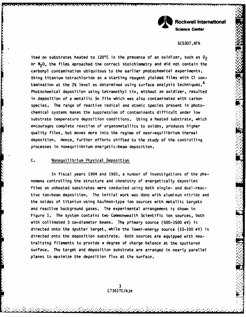
C. Noneguilibrium Physical Deposition
In fiscal years 1984 and 1985, a number of investigations of the phe-
nomena controlling the structure and chemistry of energetically deposited
films on unheated substrates were conducted using both single- and dual-reac-
tive ion-beam deposition. The initial work was done with aluminum nitride and
the oxides of titanium using Kaufman-type ion sources with metallic targets
and reactive background gases. The experimental arrangement is shown in
Figure 1. The system contains two Commonwealth Scientific ion sources, both
with collimated 3 cm-diameter beams. The primary source (500-1500 eV) is
directed onto the sputter target, while the lower-energy source (10-100 eV) is
directed onto the deposition substrate. Both sources are equipped with neu-
tralizing filaments to provide a degree of charge balance at the sputtered .*,-
surface. The target and deposition substrate are arranged in nearly parallel
planes to maximize the deposition flux at the surface. .'
3C7361TC/bje
• _ _.• - -- _ - ; " ft, .' '-' - *. t. - ..- ..t .- f ." f, t ,' *. "- ft ' .. , ft- , • .. " . - t,- , - . ,t. .. - -m- fm mt ifm m t mlm itf

I 9 Rockwell InternationalScience Center
SC5307.4FRSM$-33S13
SECONDARYH ION GUNHEAT .
LAMP. ... _.
PRIMARY TARGET
IONGUN I.
PLANETARYSUBSTRATE HOLDER
Fig. 1 Chamber geometry for single- and dual-beam deposition experiments.
The deposition chamber, designed and developed in this laboratory 5 is
fully UHV compatible with all copper gasket seals and is pumped by two Balzer
turbomolecular pumps (510 and 330 l/s). With bakeout, the base pressure in
the chamber is 3 x 10⁻⁹ torr. Gases for the experiments were either Matheson
research grade in 1 liter glass flasks or AirProducts pre-purified grade in . -
steel cylinders. Gas compositions were routinely checked by a residual gas
analyzer.
1. Titanium Oxide Films
The titanium oxide films were initially studied for direct comparison
with TiO 2 films produced previously in the photochemical studies. The films
were deposited from 99.7% purity metal targets using argon as the primary
sputtering gas. Oxygen was added to the films by backfilling the chamber to
4C7361TC/bje

$' Rockwell IntemationalScience Center
SC5307.4FR '
i , 2 x 10⁻⁵ torr. The 02 was not run through the Kaufman sources which extended -"
the lifetimes of the filaments. Films were deposited on single-crystal sili-
con, glass slides, and cleaved single-crystal NaCl and KCl. The deposition
experiments on the soluble salt substrates were carried out to provide samples
for transmission electron microscope analysis and for a post-deposition
annealing study of TiO 2 carried out under a complimentary internal research6
project.
The TiO x films formed by single reactive ion-beam deposition were
amorphous to the limit of analysis by x-ray and electron diffraction and
routinely showed an oxygen deficiency as determined by x-ray photoelectron
spectroscopy. Dual-beam films showed some fine polycrystalline structure.
TEM analysis of the films, as floated from the NaCl and KC1 substrates, showed
that there is an inverse correlation between the magnitude of the measured
refractive index and the distribution of extremely fine porosity in the films.
Energy-dispersive x-ray (EDX) analysis confirmed that the included porosity
contained Ar. Films with an index of 2.36 at 633 nm, prepared by dual ion-
beam sputtering, showed a factor of 6 greater Ar content than single ion-beam
deposited films with an index of 2.42.
The possibility of forming large-grained crystalline films by post-
deposition annealing of amorphous TiO 2 was investigated under IR&D sponsor-
ship to determine if the two-dimensional restrictions placed upon grain devel-
opment in very thin films could be used to enhance orientation and ordered *.
grain growth, independent of substrate characteristics, to produce films with
properties approaching those of a single crystal. Some of the significant
observations from this study were:
1. The dominent factors in the crystallization were found to be the
thickness and density of the films.
2. 100 nm-thick films annealed free-standing (on nickel grids) and those
transformed on substrates showed essentially the same orientation
5C7361TC/bje
, :............ .. .. .' :. :.._. . ' . . .. .;' ..... .- . -. ,'.:'.';"": ,-. -.---. . "..'

- -
Rockwell IntemationalScience Center
SC5307.4FR
behavior, indicating minimal substrate contributions to grain growth
behavior. Films that had been grown on a rotating substrate and
those that had been grown on a stationary substrate also showed
similar annealing patterns.
3. Oriented large-grain development is controlled by the competition
between individual grain nucleation and their subsequent growth.
High temperatures lead to increased nucleation site formation and
rapid transformation, while lower temperatures favor limited
nucleation sites and hence the growth of large grains.
The effect of film thickness on crystallization is dramatic. Figure
2 shows a TEM micrograph of a 26 nm film annealed for 15 h at 5000C. Films of
this thickness showed only very local transformation into submicron polycrys-
talline grains at 4000C, remaining primarily amorphous even at annealing times
of 104 h. At 500-C, these films fully transformed into void separated submi-
cron crystallites. Grain growth is limited by the formation of voids, as the
density changes in the transforming material cannot be accommodated. Thehigher temperatures involved in the transformation lead to the formation of
multiple crystalline phases including anatase, brookite, and rutile.
With increasing film thickness (> 30 nm), local transformation
occurs, yielding well-formed ellipsoidal single crystallites of anatase with
their a-axis normal to the substrate plane (Fig. 3). The individual crystal-
lites, forming as islands in the amorphous film, grow together with longer
annealing times.
At thicknesses of 90 to 160 nm, the films completely transform to
anatase at temperatures above 3700C after only 4 h. The transformation - -
produces (100) oriented anatase grains 5 to 20 on in length (Fig. 4). The
nearly parallel step structure in some of the narrow grains is characteristic
of the interfacial control of the growth mechanism, in which porosity regu-
larly segregates to cellular boundaries. The degree of misorientation between
the adjacent parallel grains is generally less than 20.
6C7361TC/bje

9il Rockwell InternationalScience Center
SC5307.4FR
SC85-33M
Fig. 2 TEN micrograph of void-limited grain growth in 26 nm TiO 2 film afterannealing to 5000C for 15 hours. Needle-like grains are brookite,large grains anatase, and the smaller spherical particles rutile.
SC85.33M9
2M
Fig. 3 TEN micrograph of single-crystal <100> anatase forming in planeof 61 nm-thick TiO 2 film, after 15 hours at 4000C.
C7361TC/bje
........ .. .. .. .. .. .. .................

INIM
Rockwell InternationalScience Center
SC5307.4FR
Fig. 4 Fully crystalline 100 nm-thick anatase TiO 2, annealed free-standingat 400%C in Ar for 15 hours.
2. PUZT Films
Amorphous films have desirable properties for some optical applica-
tions. Stress and impurities in such films are uniformly distributed, and
they do not suffer from birefringence and scattering as can large-grain poly-
crystalline materials. However, for most electrical or electro-optical appli-
cations, the optimal properties of a material can only be achieved if it
exists in its single-crystal form. Having demonstrated the ability to form
amorphous, polycrystalline, and near single-crystal films under different
conditions in the TiO study it was decided to change the emphasis of this
2i
research toward the deposition of a more complicated electro-optically active
multication film. In such a film any success in creating oriented crystalli-
zation could be determined directly through measurements of the dielectric
constant. We choose to study lanthanum-modified lead zirconate-titanate
(PLZT) because of its importance as an electro-optic material and because a
8C7361TC/bje

' j 4 Rockwell Intem ational P-Science Center
SC5307.4FR
significant literature already existed concerning its production by other
deposi ti on techniques.
PLZT is a transparent ferroelectric material having an exceptionally
strong electro-optic effects. The stoichiometry of this quaternary system,
Pbl.xLax(ZryTiz)l.x/403, is normally abbreviated as PLZT(x/y/z) where
y + z = 1.
For device applications, PLZT is usually employed in the form of
thinned ceramics that require high operating voltages because of their thick-
ness and considerable cost for the microfabrication processing. For these
reasons, there has been considerable effort to produce thin film PLZT. This
has been done using electron-beam evaporation and rf sputtering where most of
the recent work has employed the latter technique.
Although a second-order electro-optic effect has been observed for
amorphous thin films, in order to show strong linear electro-optic effects and
a high dielectric constant the film must have large perovskite grains
(1-2 on). This has usually been accomplished by either growing the films on a
heated substrate at 350 < T < 550 0C and post annealing to 650 < T < 800 0C or
by epitaxially growing the films at 500 < T < 7000C onto a suitable single-
crystal substrate.
Ion-beam deposition is conducted at pressures that are one to two
" orders of magnitude lower than those needed for rf sputtering so that the
depositing particles have considerably higher kinetic energies. One might
" expect that for a given substrate temperature, ion-beam deposition could pro-
duce a higher density film and thus that the subsequent annealing temperature
*. could be reduced.
Ion-beam sputtering is a nonequilibrium deposition technique and the
stoichiometry of the films produced may not equal that of the sputtering
target. We therefore attempted to study how the film stoichiometry varies
with deposition parameters.
9C7361TC/bje

9 Rockwell internationalScience Center
SC5307.4FR
PLZT ceramic targets with known stoichiometries were prepared by sol-
gel techniques and consolidated by hot isostatic presssing (HIP). Gels of the
desired composition were prepared from zirconium isobatylate and titanium
isopropoxide mixed with water solutions of lanthanum and lead nitrate. The
gels were dehydrated, then fired to 600C to remove all organics while retain-
ing reactivity in the calcines. These reactive powders'were then cold-isosta-
tically pressed into 5 cm-diameter cylindrical green bodies 0.5 cm tall,
wrapped in nickel foil and placed in stainless-steel pouches. The HIP con-
tainers were heated under vacuum to 4000C and vacuum sealed by welding. Final
consolidation was carried out in the HIP furnace at 12000C and 168 MPa pres-
sure of argon. The ceramics were removed from the HIP containers, and pol-
ished to serve as sputtering targets. The sample used in most of this work
was made with the stoichiometry Pbj.00 Lao.0 85Zro.63T0 .3503.
The films were grown in the UHV deposition chamber into which a
planetary substrate holder and a quartz heat lamp were added (see Fig. 1).
Before each growth, the chamber was pumped down to <2 x 10⁻⁷ torr where H20
remained the primary residual gas. The chamber was then backfilled to
2 x 10- torr with oxygen while 5 sccm of argon was flowed through each of the
ion guns to bring the total chamber presure up to 2 x 10⁻⁴ torr. With a
shield over the substrates, a ceramic PLZT (9/65/35) target was sputter
cleaned for 5 minutes with the 1000 eV primary ion beam. Then with the
primary ion beam off and the substrate shutter retracted, the substrates were
cleaned for 5 minutes with - 0.1 mA/cm2 of 500 eV argon ions from the second-
ary ion gun. The secondary ion gun was then only used during dual ion-beam
deposition runs. With a primary ion current of 30 mA, the growth rates were
5 nm/min and the thickness uniformity over the 4 cm2 substrates was better
than 3%.
The stoichiometries of the deposited films were measured by x-ray
photoelectron spectroscopy. For these measurements, peak heights were used
and were normalized to the spectrum of the known stoichiometric PLZT ceramic.
Each sample was first given a light sputter cleaning for 2 minutes with a
10C7361TC/bje
" ''" **-"*"'"" ' * "" "7 ""
. .- . ,. . .,*.', . ,- ,, . - . . .. . - ,. • ** ,.*. .. , . ,-. ,,., -,% -, .

Rockwell IntemationalScience Center
SC5307.4FR
2.5 keV argon ion beam. A typical spectrum is shown in Figure 5. The rela-
tive concentrations of the four metals equalled that of the target to within
10%. When a 50 eV secondary ion-beam was used during the film growth, the
concentrations again remained similar. However, with the secondary ion gun
operating at 500 eV during dual ion beam deposition or with the planetary
tilted so that some of the 1000 eV primary ions were hitting the substrates,
the Pb concentration dropped by a factor of five while the ratio of the other
three metals remained constant. Heating the substrate to 2000C during growth
has no noticable effect upon the stoichiometry. This ability to produce a
near equivalent composition in target and deposited film on the low-tempera-
ture substrates was encouraging in that previous workers7,8 depositing PLZT by
diode sputtering have reported the necessity of incorporating excess PbO in
their targets in order to achieve proper stoichiometry. The higher substrate
temperature employed by these workers (6000C) was probably responsible for the
lower sticking coefficient or the reevaporation of Pb from their films. In
addition, the formation of a low-temperature deposited amorphous film can
significantly increase reactivity and lower transformation temperatures in
post-deposition annealing, as was found with the TiO 2 studies.
The index of refraction of our films at 633 nm was measured with a
Gaertner auto-gain ellipsometer. Films were yrown on Si substrates for these
measurements. Indexes of 2.2-2.4 were measured for the single-beam films and
2.1-2.2 for the dual-beam films. Comparing to an index of 2.5-2.6 obtained
for epitaxially grown films9 ,10 implies that these sputter-grown films are
considerably less dense. However, rf-sputtered PLZT (8/65/35) has exhibited
an electro-optic effect despite an optical index of 2.1.11
The optical transmission spectrum of a 240 nm-thick single ion beam
film on fused SiO 2 is shown in Figure 6, where the substrate spectrum has been
divided out. Figure 7 shows the optical spectrum of a 340 nm-thick dual-beam
film. If the interference effects are accounted for, the dual-beam spectrum
is > 95% transparent down to ~ 400 nm while the single beam spectrum shows a
loss of transmission throughout the visible. The high energy cut-off of the
dual beam film shifts 10 nm found the uv upon annealing.
IIC7361TC/bje
- . - - - - - - - -- -. K v:. -> ** .*. * . " JK \*-i

Rockwell InternationalScience center
SC5307.4FR
I 3
I
F ,I is I P I 41
20000 ta~e O(v b/; -
fI22
I Pb(4--
3/2 5'
3/2 3/2
: c c oJ 2 3*
a 20 1 60C .00 2CC C3-I>D-I ... E G' (e '"
Fig. 5 XPS spectrum of PLZT film taken with Mg K. radiation.
,.01,,,,, ,.'-
W r°--
PLZT/FUSED S'0 2 ,."-
200 300 400 boo 000 700
WAVELENGTH (nm,
Fig. 6 Transmission spectrum of 240 nm-thick single ion-beam PLZT.
12C736ITC/bje

9il% Rockwell InternationalScience Center
SC5307.4FR
1.0
I As DEPOSITED ANNEALED
700T 14 MRS
DUAL BEAMPLZTIFUSED Si02
200 300 400 500 600 700 8ooWAVELENGTH inm)
Fig. 7 Transmission spectrum of 340 nm-thick dual-beam PLZT film before andafter annealing to 7000C for 14 hours.
As-deposited rf-sputtered films12 show optical transmission spectra
similar to our single ion-beam film. Annealing of the rf-sputtered films
improves the transmission so that the spectra then resembles our as-deposited
or annealed dual-beam films.X-ray diffraction measurements of 300 nm-thick single ion-beam films
4 on fused silica substrates showed no structure. When a similar dual ion-beam
film (index = 2.2) was annealed at 7000C for 14 h in the presence of PbO
powder, one diffraction peak at 30.50 was recorded. This maximum of the peak
corresponds to the (110) diffraction peak of Perovskite-type PLZT,8 ,12 which
is the largest peak in the Perovsklte PLZT spectrum, but overlaps the strong
30.0° peak of the cubic pyrochlore form of PLZT. The measured width (1.60
fwhm) corresponds to an average crystallite size of 12 nm. Subsequent anneal-
ing of the same film to 800% for 2 hours had no effect on the spectrum,
Indicating that some mechanism was preventing grain growth in the films.
13C7361TC/bje
-7°

Rockwell IntemationalScience Center ..1.W
SC5307.4FR
To measure the dielectric constant, a 300 nm-thick film was deposited a">
on a conductive indium tin oxide coated glass substrate. 80 nm of aluminum
was then evaporated onto the film through a mask. This created a pattern of
1.0 mm diameter dots. The capacitance of a given dot was then measured at
1 kHz using a HP 4262A digital LCR meter. Dielectric constants for all films .-.
were between 25 and 35, even after annealing. This is to be compared with
values greater than 1000 previously obtained for perovskite-type PLZT thin
films. Low dielectric constants are indicitive of either a pyrochlore-type
PLZT structure or a multi-phased material.
Transmission electron microscopy (TEM) was used to examine the film
microstructure and the film crystallization process. 50 nm-thick films were
deposited on freshly cleaved NaCi and KCI substrates, floated off, and mounted
on nickel grids for TEM analysis and annealing. The single-beam as-deposited
films, produced on a nonrotating substrate, showed a unique electron contrast
pattern when observed by TEM. The fully amorphous films had parallel-llne
contrast patterns, as shown in Figure 8. The spacing of the parallel features -
are on the order of 12 nm. The large dark spheres are deposits on the surface
from the NaCl substrate, while the lighter 1-2 nm spherical shapes are
distributed argon-filled porosity in the film.
The contrast patterns in the amorphous PLZT have not been satisfac-
torily explained, though they can only arise from either a highly regular
thickness-density variation or an electro-magnetic interaction of the beam
with the film. Since any substrate feature replications or extremely regular
thickness-density variations are highly unlikely on this scale, it is quite
probable that the contrast variation is associated with the electro-optic
properties of the PLZT. The absence of any such contrast variations in dual-
beam, rotated, or annealed samples also indicates that the effect is probably
associated with short-range molecular ordering occurring only in the nonro-
tated single-beam film. This phenomena is quite interesting, and will be
investigated further.
14C7361TC/bje
w* W . '' a '"% "". "- . . '- . "- ,, ,'- , , - ." - . " - , "- . "- . ". , "."- . '/ . . . , ".", , -.- . -. ". , , , , . . .
' Rockwell IntemationalScience Center
SC5307.4FR
8s864=s1
,.. °,
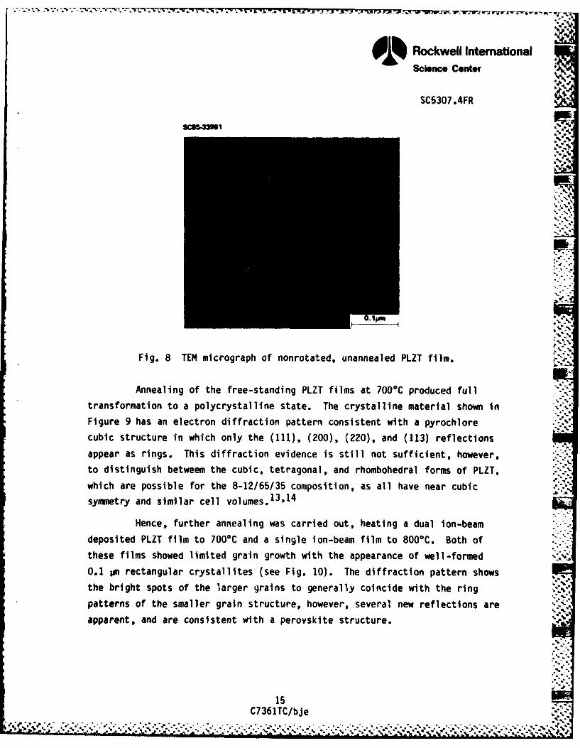
Fig. 8 TEM micrograph of nonrotated, unannealed PLZT film.
Annealing of the free-standing PLZT films at 7000C produced full
transformation to a polycrystalline state. The crystalline material shown in
Figure 9 has an electron diffraction pattern consistent with a pyrochlore
cubic structure in which only the (111), (200), (220), and (113) reflections
appear as rings. This diffraction evidence is still not sufficient, however,
to distinguish betweem the cubic, tetragonal, and rhombohedral forms of PLZT,
which are possible for the 8-12/65/35 composition, as all have near cubic
symmetry and similar cell volumes. 13 ,14
Hence, further annealing was carried out, heating a dual ion-beam
deposited PLZT film to 700C and a single ion-beam film to 8000C. Both of
these films showed limited grain growth with the appearance of well-formed
0.1 ou rectangular crystallites (see Fig. 10). The diffraction pattern shows
the bright spots of the larger grains to generally coincide with the ring
patterns of the smaller grain structure, however, several new reflections are
apparent, and are consistent with a perovskite structure.
15C7361TC/bje

'Rockwell InternationalScience Center
SC5307 .4FR8c5-3=S7
Fig. 9 TEM micrograph of free-standing PUZT film that has been annealedat 7000C for 15 hours.
1JM
Fig. 10 TEM iucrograph of free-standing, single ion-beam PUZT film that hasbeen annealed to 800% for 2 hours.
16C7361TC/bje

9il Rockwell IntemationalScience Center
SC5307.4FR
This indicates that temperatures in excess of 800% are required to ;
convert the nonferroelectric cubic crystalline structure to the ferroelectric
perovskite structure in the low-temperature deposited films. This is more
than a 1500C higher firing temperature than has been required for PLZT films
deposited at substrate temperatures between 450 and 500%. g
The growth of the PLZT grains and this transition to perovskite
structure is clearly being restricted by the continuous porosity resulting Ilk
from the density changes in the film during transformation. This is a result
of the argon-filled voids produced during deposition on the unheated sub-
strates. This effect occurred in both the dual-beam and single-beam deposited
films, though the extra energy in the dual-beam deposition did produce greater
local densities, as reflected by the lower temperature needed for PLZT grain
growth. This demonstrates that adequate density is being reached in the solid
portions of the film during low-temperature deposition, but that the entrapped
argon produces voids which become interconnected porosity during annealing.
The reactive ion-beam technique provides enough surface mobility in
the deposition process to produce locally dense multication films with good
stoichiometric control, but the problem of inert-gas void inclusion limits the
useful applications with low-temperature substrates. These void inclusions
could perhaps be minimized by using a more reactive gas, such as 02 in the
primary sputter beam, but again substrate heating provides the simplest
approach to avoiding this artifact.
Future efforts in this area will emphasize the use of various sput-
tering gases and a temperature variation study to determine if void-free films
can be formed and still retain the desired amorphous structure.
17C7361TC/bJe
i, .' %". .* .. o * . . . .
. e . q o . .. ° . ,, . . . . . . ,, . . . ° . . . . ,. . - . ° . ** °. ,- . •. - , °•., o , ,

' Rockwell InternationalScience Center
.5
SC5307.4FR
FUTURE EFFORTS
Future work at the Science Center in this area will be continuing
under internal support with the efforts emphasizing the use of reactive-ion
and fast-atom beam techniques for the production of well defined stoichiome-
tries and crystalline structures in optical and electro-optical materials.
18C7361TC/bje
X . ** * ~ ~ V *~* * .,~S *. , .'

O Rockwell IntemationalScience Center
.. .1"
SC5307.4FR
REFERENCES
1. R.D. Coombe and F.J. Wodarczyk, Appl. Phys. Lett. 37, 846 (1980).
2. Annual Report for the period June 30, 1981 through Oct. 29, 1982, this
contract.
3. Annual Report No.2 for the period Sept. 1, 1982 through Aug. 31, 1983,
this contract.
4. Annual Report No. 3 for the period Sept. 1, 1983 through Aug. 31, 1984,
this contract.
5. IR&D No. 829, 1982.
6. A.B. Harker, D.G. Howitt, P.J. Hood, and P. Kobrin, in Proceedings of the
1985 Fall Materials Research Society Meeting, Boston, MA.
7. H. Volz, K. Koger, and H. Sxhmitt, Ferroelectrics 51, 87 (1983).
8. H. Matsunami, M. Suzuki, M ishida, and T. Tanaka, Jap. J. App. Phys. 15,
1163 (1976).
9. M. Okuyama, T. Usuki, Y. Hamakawa, and T Nagawa, Appl. Phys. 21, 339
(1980).
10. H. Adachi, T. Kawaguchi, K. Setsune, K. Ohji, and K. Wasa, Appl. Phys.
Lett. 42., 867 (1983).
11. M. Ishida, H. Matsunami, and T. Tanaka, Appl. Phys. Lett. 31, 433 (1977).
IN
19 . .S..C7361TC/bje

9Rockwell InternationalScience Center
SC5307.4FR
12. T. Nakagawa, J. Yamaguchi, T. Usuki, Y. Matsui, Mokuyama, and Y.
Hamakawa, Jap. J. Appi. Phys. 18, 897 (1979).
I13. E.T. Keve and K.L. Bye, J. Appl. Phys._46, 810 (1915).
*14. G.H. Haertling and C.E. Land, J. Am. Ceram. Soc. 54, 1 (1971).
WRITTEN PUBLICATIONS
*F.W. Wodarczyk, D.R. Strauss and A.B. Harker, "Comparison of Optical Coatings
Deposited by Novel Physical and Chemical Techniques," in Laser-Induced
Damage in Optical Materials: 1983, N.E. Sennett, A.H. Guenther, D. Milam,
and B.E. Newman, eds., NBS special' publication (in press).
PAPERS PRESENTED
"Comparison of Optical Coatings Deposited by Novel Physical and Chemical* Techniques," 15th Ann. Symp. on Optical Materials for High Power Lasers, Nov.
14-16, 1983, Boulder, CO.
20C7361TC/bje

Rockwell InternationalScience Center
SC5307.4FR
PERSONNEL
Alan B. Harker: Group Manager, Member Technical Staff, Applied Spec-
troscopy Group. Dr. Harker has been at the Science Center since 1973 after
receiving his B.A. in Chemistry from Oberlin College, 1968, his Ph.D. in
Physical Chemistry from the University of California at Berkeley in 1972, and
conducting a year of research at the Lawrence Berkeley Laboratories in apply-
ing x-ray photoelectron spectroscopy to the study of the interfacial reactions pof aerosol particles. During his 12 years at the Science Center, Dr. Harker
has carried out research into the kinetics and mechanisms of a number of
homogeneous and heterogeneous reaction systems primarily in environmental and
energy-related fields, and has been the principal investigator in developing a
basic research program in the application of energetic beam techniques to the
deposition of dielectric optical thin films. His work has lead to the devel-
opment of an extensive spectroscopic and microscopic capability in the Applied
Sepectroscopy Group, emphasizing the use of surface and microprobe techniques
to determine the details of interfacial reactions. Between 1974 and 1979 the
primary focus of his work was the heterogeneous reactions of atmospheric aero-
sols both in the stratosphere and troposhere, which lead to his being selected
to the FAA overview panel for determining research needs in upper atmospheric
pollution in 1978 (FAA-HAPP). Since 1978 he has been co-principal investiga-
tor in and program manager of the Science Center activities in the development
and characterization of ceramic and glass nuclear waste forms and the charac-
terization of their interactions with aqueous environments. These activities
included 3 years of participation in the DoE-sponsored Alternate Waste Form
Program, developing polyphase ceramics as an advanced nuclear waste form, and
3 years of investigating interfacial surface reactions in the DoE High-Level
Nuclear Waste Form Leaching Mechanisms Program. During the past four years,
Dr. Harker has headed a team of researchers developing energetic-fast atom and
ion-beam techniques for depositing dense amorphous films of optical dielectric
materials. These studies have recently been extended to the study of surface
modification techniques for the toughening of ceramic infrared optical mater-
21C7361TC/bje
.... .... 7.. . . . . .**-

Rockwell InternationalScience Center
SC5307.4FR
ials. Dr. Harker is a member of Sigma Xi, the American Ceramic Society, the
American Chemical Society and the Materials Research Society. He has been
recognized for his contributions to the field of nuclear waste research by
having been nominated 3 times as a co-author for the Best Paper Award in the
American Ceramic Society Nuclear Division, receiving the award in 1981, and
being selected as Rockwell Engineer of the Year in 1982. Dr Harker has
authored and co-authored over 40 technical publications and 3 patents.
F.J. Wodarczyk: Former Member of Technical Staff, Applied Spectro-
scopy Department, Illinois Institute of Technology, 1966; Ph.D., Harvard
University, 1971. Dr. Wodarczyk's background and experience range from
molecular spectroscopy and dynamics to laser physics and surface analysis.
* Doctoral work in microwave spectroscopy under Prof. E. Bright Wilson involved
in part the development of a radio frequency-microwave double resonance tech-
nique for aiding the analysis of complex spectra. Post-doctoral work at the
University of California, Berkeley, with Prof. C. Bradley Moore, dealt with
problems in energy transfer and reaction kinetics. Subsequent research at the
* Air Force Cambridge Research Laboratories involved additional studies of elec-
tronic-to-vibrational energy transfer as well as work on optically pumped
laser systems. Dr. Wodarczyk joined the Science Center staff in 1978 and has
worked on chemical laser systems and novel thin-film deposition techniques,
including laser-induced deposition of atomic and molecular films, reactive
energetic beam deposition, and the generation of metal oxide films from the
photochemical deposition of organo-metallic vapors. In his three years with
the Applied Specroscopy Group, Dr. Wodarczyk has been the principal investiga-
tor on a basic study of the nonequiibrium chemistry involved in laser-induced
adsorption and desorption of metals and organic vapors sponsored by AFOSR and
has been a coinvestigator in the Science Center's internal Optical Thin Film
Research program. Dr. Wodarczyk has contributed to 17 technical publications.
P.H. Kobrin: Member of Technical Staff, Applied Spectroscopy Depart-
ment. B.A., University of California, San Diego, 1978; Ph.D., University of
California, Berkeley, 1983. Dr. Kobrin's graduate research under the direc-
22C7361TC/bje

JK ya
Rockwell InternationalScience Center
SC 5307.4FR
tion of Prof. D.A. Shirley, involved the study of relativistic and many-
electron interactions on the photoionization of gases. These effects werestudied using continuously tunable synchrotron radiation and time-of-flight
photoelectron spectroscopy. His post-doctoral work under Prof. N. Winograd
was based on the application of multiphoton resonance ionization to the studyof neutral species ejected from ion-bombarded surfaces. Dr. Kobrin joined theScience Center in November, 1984. He has co-authored over 20 scientific
publications.
23C7361TC/bje
..................................
..........................................*,.. .

4
4
'.4.
.1
4'.
4.'
.1
4
- S.
S.-
.4-.JS.
6~5b J4~
I I
I I (
a p.
4'.
** .4 S *4 - *** *~ .~4~4. .> S -