Noise Shaping Techniques for Analog and Time to Digital ...
181
Noise Shaping Techniques for Analog and Time to Digital Converters Using Voltage Controlled Oscillators by Matthew A. Z. Straayer Submitted to the Department of Electrical Engineering and Computer Science in partial fulfillment of the requirements for the degree of Doctor of Philosophy at the MASSACHUSETTS INSTITUTE OF TECHNOLOGY June 2008 c Matthew A. Z. Straayer, MMVIII. All rights reserved. The author hereby grants to MIT permission to reproduce and distribute publicly paper and electronic copies of this thesis document in whole or in part. Author .............................................................. Department of Electrical Engineering and Computer Science May 21, 2008 Certified by .......................................................... Michael H. Perrott Associate Professor Thesis Supervisor Accepted by ......................................................... Terry P. Orlando Chairman, Department Committee on Graduate Students
Transcript of Noise Shaping Techniques for Analog and Time to Digital ...
Noise Shaping Techniques for Analog and Time to
Digital Converters Using Voltage Controlled
Oscillators
by
Matthew A. Z. Straayer
Submitted to the Department of Electrical Engineering and Computer
Sciencein partial fulfillment of the requirements for the degree of
Doctor of Philosophy
at the
MASSACHUSETTS INSTITUTE OF TECHNOLOGY
June 2008
c© Matthew A. Z. Straayer, MMVIII. All rights reserved.
The author hereby grants to MIT permission to reproduce anddistribute publicly paper and electronic copies of this thesis document
in whole or in part.
Author . . . . . . . . . . . . . . . . . . . . . . . . . . . . . . . . . . . . . . . . . . . . . . . . . . . . . . . . . . . . . .Department of Electrical Engineering and Computer Science
May 21, 2008
Certified by. . . . . . . . . . . . . . . . . . . . . . . . . . . . . . . . . . . . . . . . . . . . . . . . . . . . . . . . . .Michael H. Perrott
Associate ProfessorThesis Supervisor
Accepted by . . . . . . . . . . . . . . . . . . . . . . . . . . . . . . . . . . . . . . . . . . . . . . . . . . . . . . . . .Terry P. Orlando
Chairman, Department Committee on Graduate Students

2

Noise Shaping Techniques for Analog and Time to Digital
Converters Using Voltage Controlled Oscillators
by
Matthew A. Z. Straayer
Submitted to the Department of Electrical Engineering and Computer Scienceon May 21, 2008, in partial fulfillment of the
requirements for the degree ofDoctor of Philosophy
Abstract
Advanced CMOS processes offer very fast switching speed and high transistor densitythat can be utilized to implement analog signal processing functions in interestingand unconventional ways, for example by leveraging time as a signal domain. In thiscontext, voltage controlled ring oscillators are circuit elements that are not only veryattractive due to their highly digital implementation which takes advantage of scaling,but also due to their ability to amplify or integrate conventional voltage signals intothe time domain. In this work, we take advantage of voltage controlled oscillatorsto implement analog- and time-to-digital converters with first-order quantization andmismatch noise-shaping.
To implement a time-to-digital converter (TDC) with noise-shaping, we present aoscillator that is enabled during the measurement of an input, and then disabled inbetween measurements. By holding the state of the oscillator in between samples, thequantization error is saved and transferred to the following sample, which can be seenas first-order noise-shaping in the frequency domain. In order to achieve good noise-shaping performance, we also present key details of a multi-path oscillator topologythat is able to reduce the effective delay per stage by a factor of 5 and accuratelypreserve the quantization error from measurement to measurement.
An 11-bit, 50Msps prototype time-to-digital converter (TDC) using a multi-pathgated ring oscillator with 6ps of delay per stage demonstrates over 20dB of 1st-ordernoise shaping. At frequencies below 1MHz, the TDC error integrates to 80fsrms for adynamic range of 95dB with no calibration of differential non-linearity required. The157x258µm TDC is realized in 0.13µm CMOS and operates from a 1.5V supply.
The use of VCO-based quantization within continuous-time (CT) Σ∆ ADC struc-tures is also explored, with a custom prototype in 0.13µm CMOS showing measuredperformance of 86/72dB SNR/SNDR with 10MHz bandwidth while consuming 40mWfrom a 1.2V supply and occupying an active area of 640µm X 660µm. A key elementof the ADC structure is a 5-bit VCO-based quantizer clocked at 950 MHz whichwe show achieves first-order noise-shaping of its quantization noise. The quantizerstructure allows the second order CT Σ∆ ADC topology to achieve third order noise
3
shaping, and direct connection of the VCO-based quantizer to the internal DACs ofthe ADC provides intrinsic dynamic element matching (DEM) of the DAC elements.
Thesis Supervisor: Michael H. PerrottTitle: Associate Professor
4

Acknowledgments
I owe much to Michael Perrott, who has freely given his time to me and this work, and
who has pushed me to think hard about fundamentals, and to balance my instinct
with reason. Collaborating with him on this work has simply been a pleasure. Hae-
Sung Lee has helped guide this work in numerous ways with constant support, quite
literally from the very first day. My colleagues at MIT have provided wonderful
feedback, ideas, and friendship. I thank Belal Helal for his diligence in testing TDC
deadzones, and for first demonstrating the GRO-TDC in a system. Chun-Ming Hsu
provided many ideas for the GRO, and his excellent work on the digital PLL proved to
be a wonderful demonstration of the GRO-TDC at the system level. Matt Park and
Min Park provided invaluable feedback on the ADC, and Charlotte Lau and Kerwin
Johnson helped immeasurably with administering software.
The opportunity for me to work on this research was made possible by the generous
support from MIT Lincoln Laboratory, and for that support I am truly grateful. Mark
Gouker’s leadership, vision, and mentorship throughout the process has been both
encouraging and insightful. I am thankful to the Lincoln Scholars Program and to
Dave Shaver for their committment to fund this work, and to Tim Hancock, who
many times helpfully lent his ear as well as his constructive feedback. I thank Andy
Messier for his willingness to debug verilog code with me, George Fitch for providing
GPIB code, and also Rick Slattery, Peter Murphy, and Lenny Johnson for support
with packaging.
Thanks are in order to Frequency Electronics, Inc. for providing access to high-
quality quartz oscillators for testing the fractional / integer digital PLL. In addition,
many people in the high-speed data converters group at Analog Devices, Inc. provided
helpful guidance and resources for testing the Σ∆ ADC.
My wife, Mariah, has worked in so many ways to support my endeavors represented
here, and I cannot overstate my gratitude of her faithfulness to me and our family.
My children have kept me focused on the important priorities; they remind me each
day of small joys that would otherwise go unnoticed. Abigail has shown me the joy
5

of learning, Caleb the joy of exploration, Eliza the joy of accomplishment, and Levi,
the joy of a good night’s sleep. I am also deeply grateful to my parents, who have
given me the foundation and freedom to undertake many adventures.
There are many others to thank as well, too many to list here. So to my extended
family and friends who have supported me financially, spritually, and emotionally, I
want to sincerely say thank you.
6
Contents
1 Introduction 19
1.1 Area of focus . . . . . . . . . . . . . . . . . . . . . . . . . . . . . . . 19
1.2 Primary contributions . . . . . . . . . . . . . . . . . . . . . . . . . . 22
1.3 Thesis overview . . . . . . . . . . . . . . . . . . . . . . . . . . . . . . 24
2 Background on Time-to-Digital Converters 25
2.1 Introduction . . . . . . . . . . . . . . . . . . . . . . . . . . . . . . . . 25
2.2 TDC with gate-delay resolution . . . . . . . . . . . . . . . . . . . . . 30
2.3 TDC with sub-gate-delay resolution . . . . . . . . . . . . . . . . . . . 32
2.4 Oversampling TDC considerations . . . . . . . . . . . . . . . . . . . . 36
2.5 Oscillator-based TDC . . . . . . . . . . . . . . . . . . . . . . . . . . . 39
2.6 Gated ring oscillator TDC . . . . . . . . . . . . . . . . . . . . . . . . 42
3 Detailed GRO operation 47
3.1 Simple Gated Ring Oscillator Implementation . . . . . . . . . . . . . 47
3.1.1 GRO with inverter delay stages . . . . . . . . . . . . . . . . . 47
3.1.2 Model for skew due to oscillator gating . . . . . . . . . . . . . 49
3.1.3 Gating skew analysis . . . . . . . . . . . . . . . . . . . . . . . 53
3.1.4 Deadzone effects . . . . . . . . . . . . . . . . . . . . . . . . . 60
3.1.5 Improving the gating sensitivity function . . . . . . . . . . . . 61
3.2 Multi-Path Gated Ring Oscillator . . . . . . . . . . . . . . . . . . . . 62
3.2.1 Achieving sub-gate-delay raw resolution . . . . . . . . . . . . 63
3.2.2 Design of the Proposed Multi-Path GRO . . . . . . . . . . . . 69
7

3.2.3 Non-linearity of the Proposed Multi-Path GRO . . . . . . . . 73
4 GRO readout techniques 81
4.1 Measurement entirely with counters . . . . . . . . . . . . . . . . . . . 81
4.2 A more efficient measurement technique . . . . . . . . . . . . . . . . 83
4.2.1 Measuring frequency by tracking phase . . . . . . . . . . . . . 84
4.2.2 Robust de-glitch technique . . . . . . . . . . . . . . . . . . . . 86
4.3 Multi-path GRO-TDC implementation details . . . . . . . . . . . . . 91
4.3.1 Phase measurement of a 47-stage multi-path oscillator . . . . 91
4.3.2 Other design considerations . . . . . . . . . . . . . . . . . . . 96
5 GRO-TDC results and discussion 99
5.1 Measurement setup . . . . . . . . . . . . . . . . . . . . . . . . . . . . 100
5.2 Inverter-based GRO-TDC measurements . . . . . . . . . . . . . . . . 101
5.3 Multi-path GRO-TDC measurements . . . . . . . . . . . . . . . . . . 104
5.3.1 Delay, power, and efficiency performance . . . . . . . . . . . . 104
5.3.2 Noise shaping performance . . . . . . . . . . . . . . . . . . . . 106
5.4 Discussion . . . . . . . . . . . . . . . . . . . . . . . . . . . . . . . . . 109
6 GRO-TDC applications and discussion 113
6.1 Digital PLL for wireless communication . . . . . . . . . . . . . . . . . 113
6.2 PLL for timing synchronization . . . . . . . . . . . . . . . . . . . . . 119
6.3 Very high-resolution frequency measurement . . . . . . . . . . . . . . 124
7 Background on VCO-based quantizers 129
7.1 Common VCO-quantizer implementations . . . . . . . . . . . . . . . 130
7.2 SNDR limitations for VCO-based quantization . . . . . . . . . . . . . 135
7.2.1 Linear modeling . . . . . . . . . . . . . . . . . . . . . . . . . . 135
7.2.2 Theoretical SNR . . . . . . . . . . . . . . . . . . . . . . . . . 138
7.3 Example . . . . . . . . . . . . . . . . . . . . . . . . . . . . . . . . . . 139
8

8 VCO-based quantizer Σ∆ ADC Architecture 143
8.1 Comparison of VCO-based quantizer and comparator-based FLASH
quantizer for Σ∆ ADC . . . . . . . . . . . . . . . . . . . . . . . . . . 144
8.1.1 Implicit Barrel-Shift DEM using the VCO-based quantizer . . 144
8.1.2 Metastability . . . . . . . . . . . . . . . . . . . . . . . . . . . 146
8.1.3 Comparator Offset and Monotonicity . . . . . . . . . . . . . . 148
8.1.4 Power Supply Considerations . . . . . . . . . . . . . . . . . . 149
8.2 Modeling the suppression of VCO-based quantizer non-linearity . . . 149
8.3 Example . . . . . . . . . . . . . . . . . . . . . . . . . . . . . . . . . . 152
8.4 Conclusion . . . . . . . . . . . . . . . . . . . . . . . . . . . . . . . . . 155
9 Prototype Σ∆ ADC with a VCO-quantizer 157
9.1 Σ∆ ADC Architecture . . . . . . . . . . . . . . . . . . . . . . . . . . 157
9.2 Circuit Implementation . . . . . . . . . . . . . . . . . . . . . . . . . . 159
9.2.1 VCO-based quantizer . . . . . . . . . . . . . . . . . . . . . . . 159
9.2.2 DAC . . . . . . . . . . . . . . . . . . . . . . . . . . . . . . . . 162
9.2.3 Loop filter . . . . . . . . . . . . . . . . . . . . . . . . . . . . . 164
10 Σ∆ ADC results and discussion 167
10.1 Measurement setup . . . . . . . . . . . . . . . . . . . . . . . . . . . . 167
10.2 Measurement results . . . . . . . . . . . . . . . . . . . . . . . . . . . 169
10.3 Discussion . . . . . . . . . . . . . . . . . . . . . . . . . . . . . . . . . 171
11 Conclusion 173
9

10

List of Figures
1-1 VCO voltage-to-frequency and voltage-to-phase relationships . . . . . 20
1-2 The basic concept of a VCO-based ADC and TDC in this work . . . 21
2-1 Reference and signal pulses vs. time . . . . . . . . . . . . . . . . . . . 26
2-2 Trends of reported TDC resolution versus CMOS technology . . . . . 28
2-3 Classical delay-chain TDC . . . . . . . . . . . . . . . . . . . . . . . . 30
2-4 A cyclic TDC based on re-using delay elements . . . . . . . . . . . . 31
2-5 An Vernier TDC that effectively amplifies the input time interval . . 33
2-6 A dual-step TDC that incorporates both the delay-chain and Vernier
techniques . . . . . . . . . . . . . . . . . . . . . . . . . . . . . . . . . 34
2-7 An analog interpolating TDC that creates transitions with sub-gate-
delay spacing . . . . . . . . . . . . . . . . . . . . . . . . . . . . . . . 35
2-8 A digital technique for creating transitions with sub-gate-delay spacing 35
2-9 Comparison of TDC DC transfer characteristics . . . . . . . . . . . . 37
2-10 Classical oscillator-based TDC . . . . . . . . . . . . . . . . . . . . . . 40
2-11 Concept of the gated ring oscillator TDC . . . . . . . . . . . . . . . . 43
2-12 Barrel-shifting of GRO delay elements to achieve first-order shaping of
mismatch error . . . . . . . . . . . . . . . . . . . . . . . . . . . . . . 44
3-1 Conceptual implementation of gating a ring oscillator . . . . . . . . . 48
3-2 Transistor-level schematic of a simple GRO . . . . . . . . . . . . . . . 48
3-3 Conceptual picture of a transition that is interrupted with a disable
window . . . . . . . . . . . . . . . . . . . . . . . . . . . . . . . . . . 50
11

3-4 Conceptual illustration of how charge redistribution within a delay
element depends on the input level . . . . . . . . . . . . . . . . . . . 51
3-5 Phase trajectory skew (error) due to the physical non-idealities of gat-
ing an oscillator . . . . . . . . . . . . . . . . . . . . . . . . . . . . . . 52
3-6 Concept of how the gating skew error for an inverter-based GRO is the
sum of the skew from the positive and negative transitions . . . . . . 54
3-7 Simulation testbench to characterize Tskew as a function of θGRO . . . 55
3-8 Gating skew vs. GRO phase for stepped disable widths . . . . . . . . 56
3-9 Schematic depicting two time constants present in the charge redis-
tribution within a delay element whose output is in transition at the
disable time . . . . . . . . . . . . . . . . . . . . . . . . . . . . . . . . 57
3-10 Gating skew vs. GRO phase for stepped rise / fall times . . . . . . . 58
3-11 Peak-to-peak gating skew vs. disable width and rise / fall time . . . . 58
3-12 Simulated deadzones in the DC GRO-TDC transfer curve . . . . . . . 59
3-13 Illustration of the problem in using resistive interpolation for the GRO 63
3-14 A GRO topology with digital interpolation . . . . . . . . . . . . . . . 64
3-15 Coupled oscillators used to reduce the effective delay per stage . . . . 65
3-16 Basic concept of using multiple inputs for each delay stage . . . . . . 66
3-17 Techniques to reduce effective delay by modifying the standard inverter 66
3-18 Example for optimizing multi-path oscillator resolution . . . . . . . . 69
3-19 Delay cell topology for the proposed gated ring oscillator . . . . . . . 70
3-20 Schematic of the proposed multi-path GRO . . . . . . . . . . . . . . 71
3-21 Inverter delay cell layout for the prototype GRO . . . . . . . . . . . . 72
3-22 Delay cell layout floorplan for the prototype multi-path GRO . . . . . 73
3-23 Simulated transient voltages of the multi-path delay element outputs 74
3-24 Concept of how the overlapping skew from positive and negative tran-
sitions for a multi-path GRO significantly reduces the total skew . . . 75
3-25 Multi-path GRO skew vs. phase for typical conditions . . . . . . . . . 77
3-26 Multi-path GRO skew vs. phase for stepped disable widths . . . . . . 77
12

3-27 Multi-path GRO peak-to-peak skew vs. disable width and rise / fall
time . . . . . . . . . . . . . . . . . . . . . . . . . . . . . . . . . . . . 78
4-1 Using two counters for each output stage to keep track of the total
number of phase transitions . . . . . . . . . . . . . . . . . . . . . . . 82
4-2 Double-counting transitions in the GRO measurement . . . . . . . . . 82
4-3 Basic concept of calculating the GRO-TDC output by differentiating
phase . . . . . . . . . . . . . . . . . . . . . . . . . . . . . . . . . . . . 85
4-4 Chart showing the logical states of a standard 15-stage ring oscillator
for each of the 30 possible discrete phase states . . . . . . . . . . . . 86
4-5 Accomodating a counter with a limited range . . . . . . . . . . . . . 87
4-6 A potential phase error when the oscillator state is determined by both
registers and counters . . . . . . . . . . . . . . . . . . . . . . . . . . . 88
4-7 Combining register and latch functions into a single element . . . . . 88
4-8 Implementation of a de-glitch circuit that achieves hysteresis by relying
on the sequence of oscillator states . . . . . . . . . . . . . . . . . . . 90
4-9 Overall block diagram of efficient and robust phase measurement tech-
nique for an inverter-based GRO . . . . . . . . . . . . . . . . . . . . 90
4-10 Simulated transient voltages of the multi-path delay element outputs
when mismatch is included . . . . . . . . . . . . . . . . . . . . . . . . 92
4-11 Logical states of the 47-stage multi-path oscillator for each of the 94
possible quantized phase states . . . . . . . . . . . . . . . . . . . . . 93
4-12 A geometric view of an example multi-path GRO state . . . . . . . . 94
4-13 Re-arranging the logical states of the multi-path GRO into groups that
correspond to the 7 measurement cells . . . . . . . . . . . . . . . . . 95
4-14 Overall system block diagram for the proposed 47-stage multi-path
GRO-TDC . . . . . . . . . . . . . . . . . . . . . . . . . . . . . . . . . 96
5-1 Microphotograph of a multi-path GRO-TDC chip . . . . . . . . . . . 100
5-2 A method to create a low-noise input signal for the GRO-TDC testing 101
5-3 Measured 65,536-pt. FFT of an inverter-based GRO-TDC output . . 102
13

5-4 An example of non-linear behavior in the inverter-based GRO-TDC . 103
5-5 Measured deadzone behavior of the inverter-based GRO-TDC . . . . 103
5-6 Measured delay per stage for the multi-path GRO vs. power supply
voltage . . . . . . . . . . . . . . . . . . . . . . . . . . . . . . . . . . . 105
5-7 Measured GRO-TDC output for a 1.2pspp, 26kHz input signal . . . . 107
5-8 Measured deadzone behavior of the multi-path GRO-TDC . . . . . . 108
5-9 Raw measured GRO-TDC output for a 26kHz input signal with an
amplitude near full-scale . . . . . . . . . . . . . . . . . . . . . . . . . 109
6-1 Basic architecture of a fractional-N digital PLL . . . . . . . . . . . . 114
6-2 A general model for the fractional-N digital PLL . . . . . . . . . . . . 114
6-3 Transfer functions for the three primary contributions to the digital
PLL phase noise . . . . . . . . . . . . . . . . . . . . . . . . . . . . . . 115
6-4 Calculated phase noise of a digital PLL with 20ps TDC resolution . . 116
6-5 A fractional-N digital PLL using the GRO-TDC and quantization noise
cancellation . . . . . . . . . . . . . . . . . . . . . . . . . . . . . . . . 116
6-6 Calculated phase noise of a digital PLL with GRO-TDC . . . . . . . 117
6-7 Measured output phase noise from the prototype 3.6GHz fractional-N
digital PLL using the GRO-TDC . . . . . . . . . . . . . . . . . . . . 118
6-8 The relationship between the magnitude of the TDC input and the ran-
dom measurement error due to thermal and 1/f noise. (a) depicts the
TDC input / output transfer characteristic, and (b) generally relates
the statistical measurement jitter to the TDC input . . . . . . . . . . 120
6-9 Concept behind the proposed fractional / integer synthesizer that min-
imizes the length of time input into the GRO-TDC . . . . . . . . . . 121
6-10 Prototype implementation of the fractional / integer synthesizer . . . 122
6-11 Measured 100MHz phase noise of the prototype fractional / integer
synthesizer . . . . . . . . . . . . . . . . . . . . . . . . . . . . . . . . . 123
6-12 Concept of a multiplying delay-locked loop . . . . . . . . . . . . . . . 124
6-13 Correlation of spurs to period measurements . . . . . . . . . . . . . . 125
14

6-14 A block diagram of the implemented MDLL prototype . . . . . . . . 126
6-15 Measured -58dBc spurious performance from the MDLL prototype . . 126
6-16 Measured MDLL phase noise at 1.6GHz output frequency . . . . . . . 127
7-1 Simple VCO-based ADC . . . . . . . . . . . . . . . . . . . . . . . . . 130
7-2 First-order noise shaping of a classical VCO-based ADC . . . . . . . 131
7-3 Improved resolution by counting positive and negative transitions of a
multi-phase VCO . . . . . . . . . . . . . . . . . . . . . . . . . . . . . 132
7-4 High-speed multi-phase VCO frequency measurement . . . . . . . . . 133
7-5 Block diagram model and corresponding linearized frequency domain
model of the VCO-based quantizer . . . . . . . . . . . . . . . . . . . 135
7-6 View of an example spectrum as it passes through the VCO-based
quantizer. (a) shows the mixed-mode view with both CT and DT
spectra, and (b) shows the DT linear model with the sampler moved
to the front-end . . . . . . . . . . . . . . . . . . . . . . . . . . . . . . 137
7-7 Behavioral model illustrating the VCO quantizer non-linearity . . . . 139
7-8 Behavioral simulation results of an example VCO-based quantizer . . 140
8-1 Σ∆ feedback to suppress VCO linearity and quantization errors . . . 144
8-2 Utilizing VCO for implicit barrel shift DEM of DAC elements . . . . 145
8-3 Dependence of comparator clock-to-Q time on input voltage . . . . . 146
8-4 A model in discrete-time (a) and continuous-time (b) for the VCO-
based quantizer Σ∆ ADC with non-linearity error Enl and quantization
error Eq . . . . . . . . . . . . . . . . . . . . . . . . . . . . . . . . . . 150
8-5 Maximum in-band |H(z)| for a lowpass modulator across oversampling
ratio and loop order. The zeros are placed either at DC (dashed line)
or at locations optimal for the oversampling ratio (solid line). . . . . . 151
8-6 Model for the prototype ADC including excess loop delay and a minor
compensation loop . . . . . . . . . . . . . . . . . . . . . . . . . . . . 153
15

8-7 Behavioral simulation results of an example VCO-based quantizer Σ∆
ADC with (a) 2nd order loop filter with NTF zeros at DC and (b) 4th
order loop filter with optimized zeros for Fb = 20MHz . . . . . . . . . 154
9-1 Block diagram of the proposed ADC . . . . . . . . . . . . . . . . . . 158
9-2 Geometric view of the proposed 31-level combined VCO quantizer/DEM
and DAC . . . . . . . . . . . . . . . . . . . . . . . . . . . . . . . . . 160
9-3 Tuning characteristic for the proposed VCO-quantizer . . . . . . . . . 161
9-4 Schematic and operation of (a) DAC 1 and (b) DAC 2 . . . . . . . . . 163
9-5 Schematic of the fully differential ADC loop filter . . . . . . . . . . . 165
9-6 Operational amplifier schematic . . . . . . . . . . . . . . . . . . . . . 165
10-1 A microphotograph of the VCO-based ADC . . . . . . . . . . . . . . 168
10-2 SNR/SNDR vs. input amplitude . . . . . . . . . . . . . . . . . . . . 169
10-3 190,190 point Hanning FFT normalized to an LSB . . . . . . . . . . 171
16

List of Tables
3.1 Details of the prototype GRO inverter delay cell . . . . . . . . . . . . 72
4.1 Truth table for the de-glitch logic . . . . . . . . . . . . . . . . . . . . 89
4.2 Assignment of delay element outputs to measurement cell inputs . . 96
5.1 Summary of multi-path 11-bit GRO-TDC measured performance . . . 110
5.2 Comparison with published TDC . . . . . . . . . . . . . . . . . . . . 110
10.1 Summary of VCO-based ADC measured performance . . . . . . . . . 168
10.2 Comparison with published high-speed CT ADC . . . . . . . . . . . . 171
17

18
Chapter 1
Introduction
1.1 Area of focus
As device characteristics for analog applications are expected to steadily degrade in
future CMOS processes, there is increasing interest in developing new mixed-signal
circuit architectures that better leverage digital circuits to improve analog processing
of signals. While this trend has been occuring for some time in the form of digital
calibration of analog circuits, it is worthwhile to consider alternate paths toward this
goal. One such path is the use of time as a signal domain to perform mixed-signal
operations such as digitization of analog signals.
In this context, voltage controlled ring oscillators are circuit elements that are not
only very attractive due to their highly digital implementation which takes advantage
of scaling, but also due to their ability to amplify or integrate conventional voltage
signals into the time domain. In this work, we take advantage of voltage controlled
oscillators (VCO) to implement analog- and time-to-digital converters with first-order
quantization and mismatch noise-shaping.
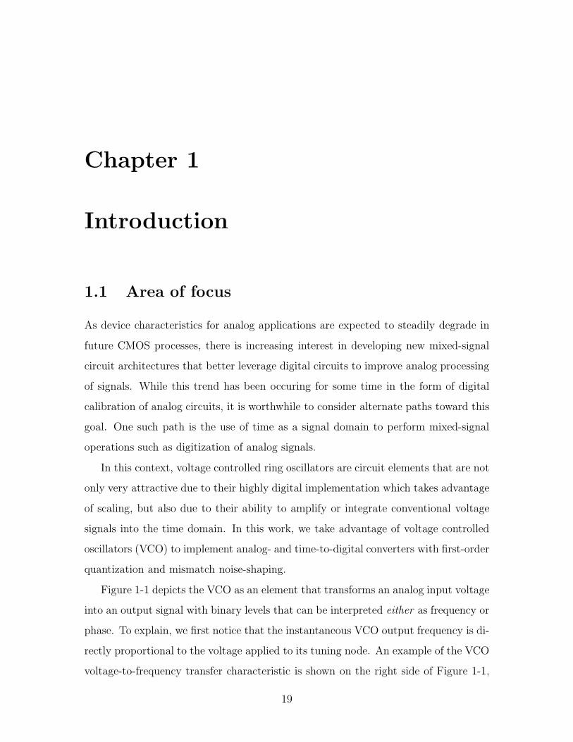
Figure 1-1 depicts the VCO as an element that transforms an analog input voltage
into an output signal with binary levels that can be interpreted either as frequency or
phase. To explain, we first notice that the instantaneous VCO output frequency is di-
rectly proportional to the voltage applied to its tuning node. An example of the VCO
voltage-to-frequency transfer characteristic is shown on the right side of Figure 1-1,
19

VCOVtune(t) Fout(t)
Φout(t)
Fout(t) = Kv.Vtune(t)
Φout(t) = 2π.Kv.Vtune(τ).dτ
t
0
F
VVtune
Fout
Kv
dFout
dVtuneKv =
Figure 1-1 VCO voltage-to-frequency and voltage-to-phase relationships
and defines the slope of the curve, Kv [Hz/V], as the small-signal voltage-to-frequency
gain. Second, we also see that the VCO effectively behaves as a continuous-time (CT)
voltage-to-phase integrator. Since the output phase of an oscillating VCO accumu-
lates without end, the VCO voltage-to-phase integration is then ideal in the sense
that there is infinite DC gain. Finally, while the phase of the VCO output signal
changes continuously, its voltage output toggles between two discrete output levels:
high voltage and low voltage. Consequently, the VCO can seamlessly drive other
digital blocks with little additional signal conditioning or amplification.
It is well-known that a simple ADC can be formed with a VCO structure by simply
adding a frequency measurement capability as depicted in Figure 1-2(a). As we will
see, the measurement circuits can be implemented a number of ways, however we can
conceptualize this circuit for now as simply counting the number of VCO periods in
each sampling clock period. The digital output of the measurement circuit will then
correspond proportionally to the input voltage through the Kv gain factor.
To implement a time-to-digital converter (TDC) with noise-shaping using the
VCO structure, we present an oscillator that is enabled during the measurement of
an input, and then disabled in between measurements as shown in Figure 1-2(b).
Note that in this case the frequency is discrete and ideally toggles between fixed
20

VCOVtune(t) Fout(t) Measurement
Circuits
CLK
Out[k]
Vtune(t)
& Fout(t)
CLK
Out[k]
(a) Analog-to-Digital
Converter
(b) Time-to-Digital
Converter
Tin[k]
0
Fosc
Figure 1-2 The concept of VCO-based converters: (a) a simple analog-to-digital con-verter, (b) a gated ring oscillator time-to-digital converter
binary values, 0 and the nominal oscillation frequency, and the analog input Tin is
now the length of time that the oscillator is enabled. The measurement circuit again
monitors the number of VCO periods or transitions that occur during the sample
clock period such that the converter output linearly corresponds with the width of
the input signal.
A very interesting aspect to both of these converter architectures is that, despite
a digital implementation, the analog quantization error for each sample can actually
be saved and passed along to the following measurement. If each sample corrects for
the error from the previous sample, then the average quantization error will improve
significantly by sampling the same input multiple times. In fact, we can say that
properly preserving and accounting for this error will result in first-order noise-shaping
in the frequency domain.
Although first-order noise-shaping is well-known and can be achieved in a rel-
atively straight-forward manner for the ADC of Figure 1-2(a), to our knowledge
21
noise-shaping for a TDC has not been previously demonstrated. In order to prac-
tically achieve good noise-shaping performance for the TDC of Figure 1-2(b), the
quantization error must be preserved during the time that the oscillator is disabled.
In fact, holding the phase state of a VCO represents a new concept outside of the
typical operating conditions for an oscillator. We therefore explore the key issues
in transferring this error, and present key details of a multi-path oscillator topology
that is able to significantly improve raw resolution and at the same time accurately
preserve the quantization error from measurement to measurement.
An 11-bit, 50Msps prototype time-to-digital converter (TDC) using a multi-path
gated ring oscillator with 6ps of delay per stage demonstrates over 20dB of 1st-order
noise shaping. At frequencies below 1MHz, the TDC error integrates to 80fsrms for a
dynamic range of 95dB with no calibration of differential non-linearity required. The
157x258µm TDC is realized in 0.13µm CMOS and operates from a 1.5V supply.
The use of VCO-based quantization within continuous-time (CT) Σ∆ ADC struc-
tures is also demonstrated, with a custom prototype in 0.13µm CMOS showing mea-
sured performance of 86/72dB SNR/SNDR with 10MHz bandwidth while consuming
40mW from a 1.2V supply and occupying an active area of 640µm X 660µm. A
key element of the ADC structure is a 5-bit VCO-based quantizer clocked at 950
MHz which we show achieves first-order noise-shaping of its quantization noise. The
quantizer structure allows the second order CT Σ∆ ADC topology to achieve third
order noise shaping, and direct connection of the VCO-based quantizer to the internal
DACs of the ADC provides intrinsic dynamic element matching (DEM) of the DAC
elements.
1.2 Primary contributions
In regard to a VCO-based time-to-digital converter, the primary contributions of this
thesis are:
• The introduction of a gated ring oscillator topology that, when used in a time-
to-digital converter, can achieve first-order noise-shaping of quantization and
22

mismatch error
• The analysis of errors due to gating an oscillator that can fundamentally limit
noise-shaping performance
• The mitigation of these errors with a multi-path ring oscillator topology that
linearizes the gating operation and reduces the effective delay per stage to a
small fraction of an inverter delay
• The presentation of techniques to efficiently and accurately measure the phase
of a multi-path ring oscillator
• The verification of first-order noise-shaping with measured results of a prototype
gated ring oscillator TDC
To our knowledge, the gated ring oscillator time-to-digital converter presented
in this work is the first TDC to demonstrate noise-shaping of analog quantization
and mismatch error for non-adjacent measurement intervals. Further, compared with
other reported TDC, the prototype described in this work is very competitive in
regard to important metrics such as dynamic range, power, and area.
Another contribution of this work is the analysis of the performance advantages,
limitations, and tradeoffs for an oversampled VCO-based quantizer, along with the
demonstration of these considerations within a high-speed continuous time Σ∆ ADC.
The idea of using a VCO for voltage quantization within a Σ∆ ADC has been pre-
sented multiple times [28, 39], and in fact the architecture chosen independently for
this work was originally disclosed in [39]. However, while the ideas for using VCO in
a Σ∆ ADC have been known for many years, this work provides measurement results
that justify the consideration of VCO-based quantizers in Σ∆ ADC. Improvements
are also discussed that may significantly improve these results, although the achieved
performance is at present competitive with other state-of-the-art ADC architectures.
Together, these contributions demonstrate the utility of ring oscillator-based quan-
tizers in achieving or advancing state-of-the-art performance for the time- and analog-
to-digital converters.
23

1.3 Thesis overview
The thesis is divided into two main parts; the first half focuses on the gated ring
oscillator time-to-digital converter in Chapters 2-6, and the second half addresses
VCO-based analog-to-digital conversion in Chapters 7-10. For both sections, we will
summarize previous work in the area, analyze and discuss the various issues that
must be addressed to achieve high resolution, and present prototype implementations
along with measurement results. Chapter 11 concludes the thesis with a few general
remarks.
The first half of the thesis begins with Chapter 2, where we provide a background
on time-to-digital converters and motivate the gated ring oscillator topology of this
work. To accomplish this, we discuss historical TDC trends, describe a number of
modern TDC architectures, and consider the benefits of oversampling before explain-
ing the fundamental concept of the GRO-TDC. In Chapter 3, we examine the accuracy
with which a digital GRO implementation can preserve analog signals from one mea-
surement to the next, and present the multi-path oscillator topology that addresses
these concerns. The measurement of the GRO with precise, efficient circuitry is dis-
cussed in Chapter 4, and measurement results are shown in Chapter 5. To conclude
the first half of the thesis, we briefly outline methods to utilize the GRO-TDC in a
number of system applications.
Chapter 7 initiates the second half of the thesis by looking at the advantages
and shortcomings of a simple VCO-quantizer. The quantizer is then placed within
a Σ∆ ADC in Chapter 8 to improve its linearity performance, and where a few
unique properties of the VCO-quantizer can be leveraged at the architectural level.
System and circuit-level details of the prototype Σ∆ ADC are described in Chapter 9,
and the presentation of measurement results along with a discussion are included in
Chapter 10.
24

Chapter 2
Background on Time-to-Digital
Converters
2.1 Introduction
Accurate measurement of time has had a critical role in the development of science
throughout history, starting with the earliest examples of analog clocks based on solar
motion and water flow, and including the most accurate caesium resonators available
today. As a subset of time-keeping technology, time-to-digital converters (TDC), or
time-interval meters (TIM), allow for precise measurement of the time between two
events. Historically, TDC have had significant application in experimental physics.
For example, in the nuclear physics community, measurements of mean lifetime, par-
ticle identification, and time-of-flight require precise TDC, and many of the early
integrated circuit TDC addressed such needs [53]. Today, TDC continue to serve an
important role not only in experimental applications, but also in commercial time-of-
flight applications such as laser rangefinding and positive electron tomography (PET)
medical imaging technology [70].
A relatively new application for TDC that has emerged is closed-loop timing sys-
tems that are fully integrated in silicon technology. Since advanced CMOS processes
have begun to offer extremely compact, robust, and flexible processing power, many
applications have begun to replace traditional analog signal processing blocks with
25

Tq
Stop
Reference
Start
t
t
Tstart
Signals
Tstop
Tin
tstart tstop
Tout
Figure 2-1 Reference and signal pulses vs. time
digital signal processing. Such a shift in architectural design places a relatively in-
creased burden on the mixed-signal interface, especially in terms of converter perfor-
mance. For systems that require precise control or alignment of timing signals, such
as phase-locked loops (PLL), delay-locked loops (DLL), and clock and data recovery
(CDR) circuits, the TDC is a fundamental element that can bridge the gap between
the continuous-time analog domain and the discrete-time digital domain.
Considering that there is an extensive history of TDC prior to the development of
digital PLL, it is useful to understand how today’s state-of-the-art TDC technology
relates to older ideas that have been around for some time. In fact, a review of the
historical developments of TDC over the past 50 years or more reveals that, while
technology has seen a tremendous change from vacuum tubes and ferrite pot-core
transformers to present-day advanced CMOS, the concepts and techniques for divid-
ing time into measureable intervals have remained remarkably the same. Given this
context, although it is possible to think of TDC architectures in terms of implementa-
tion details, it is also instructive to think of the architectures in a conceptual manner.
In this way, we can both understand current practice and, at the same time, shape
the future efforts in TDC development by considering how these simple but powerful
ideas best can be used within a new, yet undefined, component technology.
26

We then examine Figure 2-1, which is a picture describing the general operation
of a TDC that can serve as an entry point into the discussion of many different
TDC architectures and ideas. The figure, while modified slightly for our purposes,
is basically equivalent to Figure 1 from Baron’s 1957 original manuscript on the
Vernier technique [4].1 From the figure we see that the input time interval, Tin =
tstop − tstart, can be divided up into a number of smaller reference time intervals of
nominal length Tq. An estimate of Tin can be trivially calculated by counting the
number of intermediate reference pulses or events (i.e. Tout[k] = Out[k]Tq), although
there is an error to this method at both the beginning and end of the measurement,
Terror[k] = Tstop[k] − Tstart[k]. (2.1)
Given these definitions, we can express the input and output relationship for a TDC
as
Tout[k] = Tin[k] − Terror[k], (2.2)
or equivalently in terms of the TDC integer output as
Out[k] =Tin[k] − Terror[k]
Tq. (2.3)
Since the raw TDC resolution is limited by Tq, it is not surprising that a great deal
of effort over the years has been made in reducing this value, either directly through
technology advancement, or effectively by using design techniques, a few examples of
which will be covered later in the following section. While these efforts have made
significant progress in improving TDC resolution, applications continue to demand
the best resolution and/or range than can be achieved in a practical fashion.
For many early TDC applications, and especially for experimental applications,
the form factor of the TDC was less important than achieving high-resolution and
accuracy. As a result, many of the best TDC solutions in terms of resolution are large,
1We should note that within this manuscript we find that Baron ”recognizes the fact that theHughes Research and Development Laboratories, prior to the work described in this report, hadfabricated a similar vernier measuring system.”
27

(a) (b)
CMOS Process Node (µm)
TD
C L
SB
(p
s)
0.5 1 1.5101
102
103
CMOS Process Node (µm)
TD
C L
SB
/ G
ate
Le
ng
th (
ps
/µm
)
100
102
103
0.5 1 1.5
101
Figure 2-2 Trends of reported time-to-digital converter LSB resolution versus CMOSprocess technology. (a) depicts the improved resolution (decreased LSB steps) as gatelengths scale, and (b) demonstrates the relatively flat performance of TDC resolutionwhen normalized to gate length
consume significant power, and require complex tuning or calibration. For example,
in the dual-conversion approach, classic voltage-domain analog-to-digital converters
can be utilized for a TDC by integrating current onto a reference capacitor for each
input sample [68], which converts time into voltage before digitization. Although this
approach may result in excellent resolution for a particular technology, the architec-
ture is analog-intensive, is not power efficient, and does not take advantage of the
ability to resolve digital edges in modern CMOS.
In contrast, TDC constructed with digital CMOS technology have benefited greatly
from process feature scaling, since a more advanced process results in not only com-
pact and fully-integrated solutions, but also smaller CMOS gate delays and the
accompanying improvement in resolution. Figure 2-2(a) plots reported LSB size
for TDC implemented in CMOS over the last decade versus the CMOS technol-
ogy node (this work is shown with a ×), and a best-fit line to the data is also
shown [8–10, 13, 18, 19, 27, 29, 30, 34, 37, 43, 44, 46, 48, 56, 66, 71]. We can clearly see
from this data evidence that CMOS scaling has indeed resulted in better TDC reso-
lution, and assuming that at least some new process developments are made in the
28

future, TDC resolution should continue to improve.
On the other hand, Figure 2-2(b) demonstrates that when the LSB size of various
TDC are normalized to the minimum transistor gate length in the process2, the
performance of TDC has been relatively flat. While advancements have certainly
been made in adapting TDC architectures for modern CMOS, improvements to the
fundamental relationship between gate delay and LSB step size have been difficult to
realize.
Certainly one way to interpret this data is to say that the best way to achieve
an optimal TDC resolution performance is to wait, i.e. to follow Moore’s law until
scaling enables better performance with known TDC techniques. While this may be a
valid approach for some applications, it does not aid the TDC designer in optimizing
resolution performance for a given technology. Given the difficulty in improving the
raw resolution in a standard CMOS process, it then becomes important to fully
explore techniques such as oversampling to improve effective resolution performance,
which is a primary focus of this work.
Moreover, when considering future CMOS TDC and process scaling, it is well
known that transistor and parasitic mismatch has become a very real and significant
problem for the most advanced technologies [54]. Therefore, while intrinsic delay may
continue to decrease in the future, for traditional TDC architectures to benefit from
this we also require the accuracy of the delay to improve as well. We will later see
that mismatch can be a bottleneck for many TDC architectures. Therefore, achieving
high performance in the presence of large delay mismatch is a critical requirement for
future TDC that has so far seen little attention at the architectural level compared
with the relative efforts to improve raw resolution.
Since we have described some of the basic challenges facing TDC, in the next
section we will review some of the state-of-the-art TDC architectures along with
their associated performance tradeoffs. This review will lead into the focus of this
work, which is a CMOS gated ring oscillator (GRO) TDC. The GRO-TDC makes full
2Gate propagation delay is often approximated to be proportional to transistor length [81, 82],and therefore normalizing to transistor gate length is a reasonable way to normalize fundamentalresolution.
29

Stop
Tstop
StartStart
Stop
Delay = Tq
Tin
1
1
1
0
0
Out
Reg
D Q
Delay
Reg
D Q
Reg
D Q
Delay Delay
Out
Figure 2-3 Classical delay-chain TDC
use of oversampling to address the issues of limited TDC resolution in the presence
of large mismatch, while at the same time achieving a large dynamic range, compact
area, and low power consumption.
2.2 TDC with gate-delay resolution
A classic TDC architecture comprised of a chain of delay elements is shown in Fig-
ure 2-3 [2, 32], and effectively works by counting the number of sequential inverter
delays that occur between two rising signal edges. One very attractive feature of this
architecture can be seen immediately in that the TDC can be constructed entirely
from standard digital gates, as evidenced by its adoption into the FPGA commu-
nity [65, 78]. The compact and digital architecture offers a moderate performance,
and has been proved to be commercially viable for some digital PLL applications in
the wireless industry [66].
To explain its operation, the rising edge of the start signal, which represents the
first event, is successively delayed by a series of inverter gates (polarity is ignored
throughout for simplicity), each with delay Tq. The outputs from each of these in-
verters are input to a register, which is clocked with the rising edge of the stop signal
30
Stop
Start
Start
Stop
Tin
Out = 8
Out
Mux
10
DelayDelayDelay
Count
DelayOutputs
Register
Count
Logic
CountersReset
Tstop
Tq
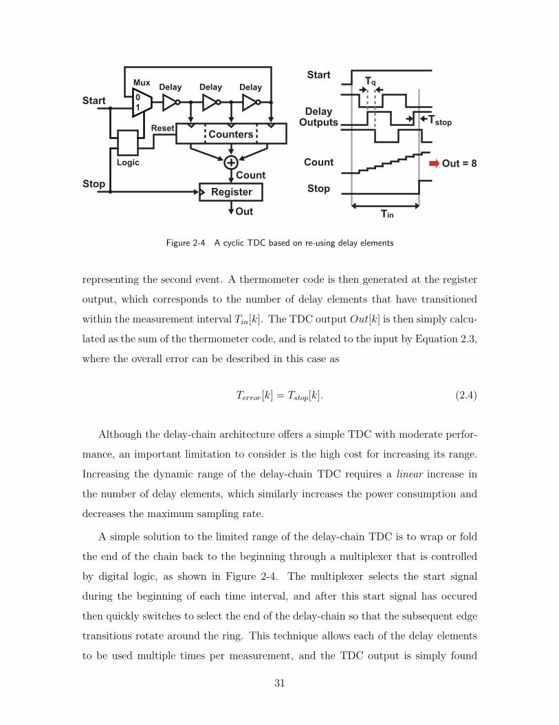
Figure 2-4 A cyclic TDC based on re-using delay elements
representing the second event. A thermometer code is then generated at the register
output, which corresponds to the number of delay elements that have transitioned
within the measurement interval Tin[k]. The TDC output Out[k] is then simply calcu-
lated as the sum of the thermometer code, and is related to the input by Equation 2.3,
where the overall error can be described in this case as
Terror[k] = Tstop[k]. (2.4)
Although the delay-chain architecture offers a simple TDC with moderate perfor-
mance, an important limitation to consider is the high cost for increasing its range.
Increasing the dynamic range of the delay-chain TDC requires a linear increase in
the number of delay elements, which similarly increases the power consumption and
decreases the maximum sampling rate.
A simple solution to the limited range of the delay-chain TDC is to wrap or fold
the end of the chain back to the beginning through a multiplexer that is controlled
by digital logic, as shown in Figure 2-4. The multiplexer selects the start signal
during the beginning of each time interval, and after this start signal has occured
then quickly switches to select the end of the delay-chain so that the subsequent edge
transitions rotate around the ring. This technique allows each of the delay elements
to be used multiple times per measurement, and the TDC output is simply found
31

by counting and summing all of the delay element transitions that occur during Tin.
Compared to the delay-chain TDC, the cyclic TDC core does not scale up at all with
larger range, and the counters will only scale with the logarithm of range.
Asymmetry in the delay-chain structure due to the multiplexer increases the mis-
match for that particular element, which degrades the differential non-linearity per-
formance. Techniques to match the multiplexer delay to that of a delay element can
be used, such as incorporating a multiplexer with fixed connections in each of the
delay elements [23]. In terms of integral non-linearity, the cyclic TDC has better
performance than the delay-chain TDC for large input signals due to the periodic use
of delay elements.
While the TDC range can be improved with the simple cyclic TDC, a more prob-
lematic issue that has not been addressed is the coarse resolution, which is limited
to a minimum inverter delay in the process. Although over time technology scaling
will improve the intrinsic delay, the mismatch of delay elements is expected to get
worse. Additionally, as mentioned in the preceding section, physical limitations due
to TDC thermal and 1/f noise will continue to be out-of-reach for resolutions limited
by a gate-delay. Therefore, an important problem to consider is how Tq of the simple
delay-chain architecture can be divided into smaller intervals in order to significantly
improve TDC resolution.
2.3 TDC with sub-gate-delay resolution
The Vernier delay technique [4] is one of the older techniques for time digitization that
has been adapted for improving the resolution of digital CMOS TDC [13,55,57], and
has been widely documented in the literature. As shown in Figure 2-5, the concept
is to effectively stretch the input time interval Tin by delaying both the start and
stop signals with delay-chains. What defines the resolution in this case is not the
absolute rate of transitions (gate-delay being equal to the number of transitions per
second), but the relative rate of transitions. As a result, the effective resolution of
the Vernier TDC is found to be the difference of the two delays, or more specifically,
32

Reg
D Q
Delay1
Reg
D Q
Reg
D Q
Delay1 Delay1
Delay2 Delay2 Delay2
Delay2
Out
1
1
1
0
0
Stop
StartStart
Stop
Delay1
Tin
Out
Tq =
Delay1 - Delay2
Figure 2-5 An Vernier TDC that effectively amplifies the input time interval
Tq = Delay1 − Delay2.
Given this result, the Vernier technique may appear to be able to substantially
improve a TDC resolution. However, there are a number of issues to consider that
practically limit the resolution improvement to a factor of 4-10. Specifically, the
same issues that are found in the simple delay-chain TDC (e.g. range, sensitivity to
mismatch) are present in the Vernier TDC, except that, along with the resolution,
the magnitude of the problems have also been amplified. Although the Vernier delay
elements may be tuned to match a fixed offset and calibrated at the system level,
such techniques are both cumbersome and dependent on system-level architecture
design [76].
To reduce the size of practical Vernier TDC, various dual step architectures based
on Vernier techniques have been proposed [27, 56, 57], as shown in Figure 2-6. These
architectures often have a simple delay-chain TDC (Figure 2-3) as the first stage, and
then further refine the initial measurement by amplifying the residual error and then
passing it to a second, higher resolution Vernier TDC. Another dual step technique
that amplifies time error using the metastability property of digital gates has also
been proposed, and in this case a larger resolution improvement up to a factor of 20
is reported [34].
33

Vernier
Stop
Start
Reg
D Q
Reg
D Q
Reg
D Q
Logic
Mux
FineOutput
Single Delay Chain
Delay1 - Delay2
Reg
D Q
Delay1
Reg
D Q
Reg
D Q
Delay1 Delay1
Delay2 Delay2 Delay2
CoarseOutput
Delay1 Delay1 Delay1
Delay1
Figure 2-6 A dual-step TDC that incorporates both the delay-chain and Vernier tech-niques
Although the range for these architectures is larger than what would be achieved
for a single-step TDC using the same resolution improvement techniques, the funda-
mental range versus size tradeoff does not improve compared with the simple delay-
chain TDC discussed earlier. Interestingly, a cyclic architecture similar to Figure 2-4
may be used to significantly increase the range of the single or dual-step Vernier
TDC [57]. In this case, the decoding logic and calibration become more complicated
due to the many logical states that are supported.
Another technique to improve TDC resolution below that of a gate-delay is to
interpolate between the input and output signals of a digital gate. Figure 2-7 il-
lustrates this concept using a resistive divider, where the undriven nodes are taken
to be the average of the delay element input and output signals. The operation of
averaging creates a new intermediate signal with a transition that effectively divides
the gate-delay into two smaller intervals. All of the new signals must be registered
appropriately, which increases the TDC size, but again a cyclic architecture can be
utilized to mitigate this issue [23]. The improvement in resolution for the interpo-
lation architecture over the gate-delay is similar to that of the Vernier architecture,
and is practically limited by the non-linear impedances of the delay elements during
34

Tstop
Start
Stop
Tq
Tin
1
1
1
1
1
Out
Stop
StartDelayDelayDelay
Registers
Out
1
0
Figure 2-7 An analog interpolating TDC that creates transitions with sub-gate-delayspacing
Start
Stop
Tq
Tin
1
1
1
1Out
StopRegisters
Out
1
0
StartDelay Delay
Delay
Figure 2-8 A digital technique for creating transitions with sub-gate-delay spacing
the switching transients.
The implementation of the interpolation architecture is not limited to resistive
ladders, and can also be efficiently realized with digital gates if the output signals are
allowed to be driven by more that one delay element. As shown in Figure 2-8, the
same averaging effect can be achieved by connecting the outputs of two delay elements
in parallel, while the two delay element inputs are staggered in time. The result from
this parallel connection is that the output impedances from both delay elements are
averaged together, which then reduces the effective delay per stage. Although this
35

architecture can also be expanded into a cyclic TDC, achieving a significant improve-
ment in resolution requires more than two delay elements to be connected in parallel,
which then increases the complexity of the multiplexer significantly. Nonetheless, we
will later see in Chapter 3 that these techniques can be modified when constructing
an oscillator-based TDC, and can in fact be to be quite useful.
For each of the Nyquist TDC architectures described so far, we have seen that
significant effort is required to reduce the TDC resolution below that of a gate-delay,
and in each case the cost for doing so is increased complexity, area, and/or mismatch.
Another common thread to these converters is that there is a deterministic map-
ping from a given input signal onto a series of delay elements. Since we know that
significant element-to-element delay variations due to mismatch cause quantization
errors that are non-linear, calibration is very much required for such converters that
hope to have resolution far below that of a gate-delay [23, 34, 66]. In a practical im-
plementation, although calibration does generally improve resolution performance in
the presence of mismatch, it is an added complexity that can significantly increase
TDC area and power comsumption. Further, while calibration is quite effective at
improving integral non-linearity, it is very difficult to completely remove differential
non-linearity errors.
2.4 Oversampling TDC considerations
From the examples described in the previous section, we clearly seek TDC implemen-
tations not only with excellent resolution, but also with inherently robust sensitivity
to issues such as mismatch. It is in this context that we proceed to consider how
oversampling may be used to improve TDC performance.
Oversampling describes the quantization of a signal with fixed bandwidth (Fb) at
a speed Fs much faster than the Nyquist rate required to reconstruct the original sig-
nal without aliasing. Because we often assume that the quantization error, Terror, is
random and uniformly distributed over the quantization step, linear system analysis
is commonly applied to compute the quantization noise power spectral density (PSD).
36

AveragedTDC
Output
Tq
TDC Input
Deterministic
(a)
Tq
TDC Input
"White" quantization
error
(c)
Tq
TDC Input
Deterministicwith minimal noise
(b)
Figure 2-9 The DC transfer characteristics for (a) a completely deterministic TDC, (b)a deterministic TDC with small jitter either due to thermal noise or the input, and (c) aTDC with ”white” quantization error due to inherent error scrambling or external dithering
Such standard analysis in the frequency domain assumes that the resulting quantiza-
tion error is spectrally white and that its PSD in discrete time ideally decreases with
sampling rate,
PSDerror =T 2
q
12Fs. (2.5)
It is then expected that filtering of the converter output to remove the undesidered
bandwidth will also remove a similar proportion of quantization noise, thus realizing
the improved signal-to-noise ratio that oversampling can ideally provide.
However, as just mentioned, such analysis depends on the quantization error being
random and uniformly distributed over the quantization step, which is not true in
general for quantizers with small input signals. As we saw earlier, an important
characteristic of the delay-chain TDC is that, since there is no error at the beginning
of the measurement (Equation 2.4), the output and error for each measurement are
deterministic functions of the input. As a result, the DC transfer characteristic of an
ideal delay-chain TDC shown in Figure 2-9(a) reveals a non-linear staircase function.
For this class of deterministic converters, there is no inherent scrambling of the TDC
error that generally can be used to improve effective resolution through oversampling.
In practice, even for deterministic TDC, there is a small amount of noise from
both the input signal and the TDC itself that will round off the edges of this staircase
37

function. As shown in Figure 2-9(b), the resulting DC transfer characteristic is now
smoothed somewhat, although the staircase non-linearity can still be evident. In fact,
a linear DC transfer characteristic (i.e. a random quantization error) can be achieved
in a deterministic quantizer only if the input signal is sufficiently large compared to
the quantization step size, which includes the situation where the input signal itself is
noisy, or if the physical noise internal to the converter is larger than the quantization
step size. This condition is illustrated in Figure 2-9(c).
In a closed-loop system such as a PLL, there are certain conditions in which the
system may provide such scrambling of the TDC input, for example as it may in a
fractional-N Σ∆ PLL. However, there are many applications to be aware of that do not
provide such a dithering. For example, the TDC input for high-performance integer-
N PLL limits to a very small range with very little deviation or noise, and a lack of
random error in deterministic TDC can be a significant problem. This situation can
be compared to the classic dead-zone in an analog phase detector, which is well-known
to cause erratic limit-cycle behavior in integer-N PLL.
One solution to this problem is to intentionally modulate the TDC input with a
sufficiently noisy signal in order to improve the randomness of the quantization error.
Of course, adding unknown noise to a TDC input is a rather poor way to linearize
the quantization. Instead, if the “noisy” signal is known and the gain of the TDC
is well-characterized, this “noise” can then be subtracted from the TDC output,
which ideally would result in a random error that can benefit from oversampling.
However, we note that the uncalibrated or residual non-linear quantization error due
to mismatch will not be corrected with averaging or filtering, since these errors will
already have folded in the sampling process to corrupt the bandwidth of interest.
For example, let us consider a high performance Vernier TDC running at 50Msps
that has been optimized at the system level to detect small input signals by mod-
ulating Tin with a psuedo-random noise source. We can assume that Tq has been
improved by a factor of 4 from the raw gate-delay of 20ps to reach 5ps resolution.
Further, a run-time calibration circuit has been designed that allows for compensa-
tion of the psuedo-random input sequence and delay element mismatch. Through
38
this calibration, the effect of mismatch has been reduced from a delay error standard
deviation of 10% to an absolute error standard deviation of only 1%, an improvement
of over 20dB. The overall rms TDC quantization error for a fixed 50kHz analog band-
width (typical bandwidth for a Σ∆ PLL) can then be estimated by the rms sum of
quantization noise and mismatch error as
Terrorrms=
√
√
√
√
T 2q (2Fb)
12Fs
+ (Tmm−rms)2 (2.6)
=
√
√
√
√
(5 × 10⁻¹²)2(1 × 10⁵)
12(50 × 106)+ (200 × 10−15)2 (2.7)
= 210fs (2.8)
While this result is relatively impressive, it is important to notice two aspects of
this example that may be cause for some concern. First, while the rms error due to
mismatch without oversampling is negligable, it becomes a dominant source of error
once oversampling is leveraged. Since the level of mismatch is only expected to get
worse in future CMOS processes, we can now see that this poses a bottleneck for im-
proving the performance of deterministic TDC in the future. The second issue in this
example is the level of complexity that was required to achieve the result, both at the
component and system levels. As we will soon see, a much simpler TDC implementa-
tion in the form of an oscillator has the benefit of inherently scrambled quantization
and mismatch error, which makes it well-suited for oversampling applications.
2.5 Oscillator-based TDC
Figure 2-10 illustrates the classical ring oscillator-based TDC composed of a ring of
delay elements [46,59], which shares a number of characteristics with the cyclic TDC
from Figure 2-4. First, we note that for both topologies the oscillator transitions are
counted during the input time window Tin, here designated by the Enable signal.
Next, all counter outputs are summed together and stored as the TDC output before
being reset (during Enable low) to prepare for the next measurement. Finally, due
39

Stop
Start
Out
DelayDelayDelay
Register
Count
Logic
CountersEnable
Enable
Count
Tin[k]
Out 6 7
OscillatorPhases
Tstop[k-1] Tstop[k]
-Tstart[k] -Tstart[k+1]-Tstart[k-1]
Tq
Tin[k-1]
Figure 2-10 Classical oscillator-based TDC
to the logarithmic scaling of the counter range, the oscillator-based TDC also has the
attribute of a large dynamic range with reasonable silicon area.
A key difference between the two architectures, however, is found when examining
the overall quantization error for the oscillator-based TDC. We find that counting
the transitions of a free-running oscillator results in error equivalent to the funda-
mental expression given earlier by Equation 2.1 and repeated here for convenience,
Terror[k] = Tstop[k] − Tstart[k]. Compared with the delay-chain or cyclic TDC error
from Equation 2.4, we now include both Tstart and Tstop, which indicates that each
measurement of the oscillator-based TDC will have an additional error contribution
from Tstart. For our purposes, we can assume that the oscillator phase at the be-
ginning of each sample is random, and subsequently Tstart is also random having
uniform density on the interval [0, Tq]. By way of contrast, the cyclic TDC ”phase”
is effectively set to 0 at the beginning of each measurement.
To have benefit from oversampling, we thankfully do not require the overall TDC
error Terror to also be a random variable with uniform density, as in fact this criteria
is quite difficult to satisfy for small inputs. Rather, we require Terror to be a white
random variable with flat power spectral density (PSD) across all frequencies and for
all inputs, including zero frequency. In addition, we require Terror to be uncorrelated
40

with Tin. Discussion of the special cases, for example where Tin is exactly equal to an
integer multiple of Tq (i.e. Terror = 0 ∀ Tin = kTq), will be postponed until later, using
the justification for now that this special case ideally occurs with zero probability and
can therefore be ignored.
Due to the random properties of Tstart, the oscillator-based TDC satisfies the
above criteria for Terror. We can expect that the small penalty of larger error for the
inclusion of Tstart can be easily offset by the resolution improvement by oversampling.
Interestingly, the oversampling benefit in the oscillator-based TDC is not constrained
to simply improving the quantization error, but also extends to improving errors from
mismatch as well.
To further explain how mismatch is also improved by oversampling, we first con-
sider an input Tin that is less than an oscillator period. As mentioned earlier, the
oscillator starting phase is random with uniform density, which implies that the delay
elements that transition during the Enable window are chosen with a white random
process that is independent of the input. Therefore, input intervals that are a fraction
of the oscillation period will have mismatch error with flat power spectral density.
Next, we can consider intervals of Tin that are longer than an oscillation period.
In this case, Tin can be seen as an interval composed of two parts: an integer number
of periods, which does not contribute mismatch error, and the residual fraction of a
period that does have mismatch contribution. The argument from the first case can
again be used on the residual part of the input with length of less than a period. As
a result, we can conclude that for inputs of any length, mismatch error is reduced
through oversampling and has no contribution towards integral non-linearity for the
oscillator-based TDC.
At this point another example is helpful to quantitatively compare a simple
oscillator-based TDC with raw resolution of a gate-delay resolution with the sub-
gate-delay approaches discussed earlier. For this example, let us consider the same
sample rate of 50Msps, analog bandwidth of 50kHz, gate-delay of 20ps, and mis-
match of 10%. Since we will rely on oversampling to reduce mismatch, we can also
assume that there is no calibration. With these parameters set, the overall rms TDC
41
quantization error is found to be
Terrorrms=
√
√
√
√
2Fb
Fs
(
2(T 2q )
12+ 2(Tmm−rms)2
)
(2.9)
=
√
√
√
√
1 × 10⁵
50 × 106
(
2(20 × 10−12)2
12+ 2(2 × 10⁻¹²)2
)
(2.10)
= 367fs. (2.11)
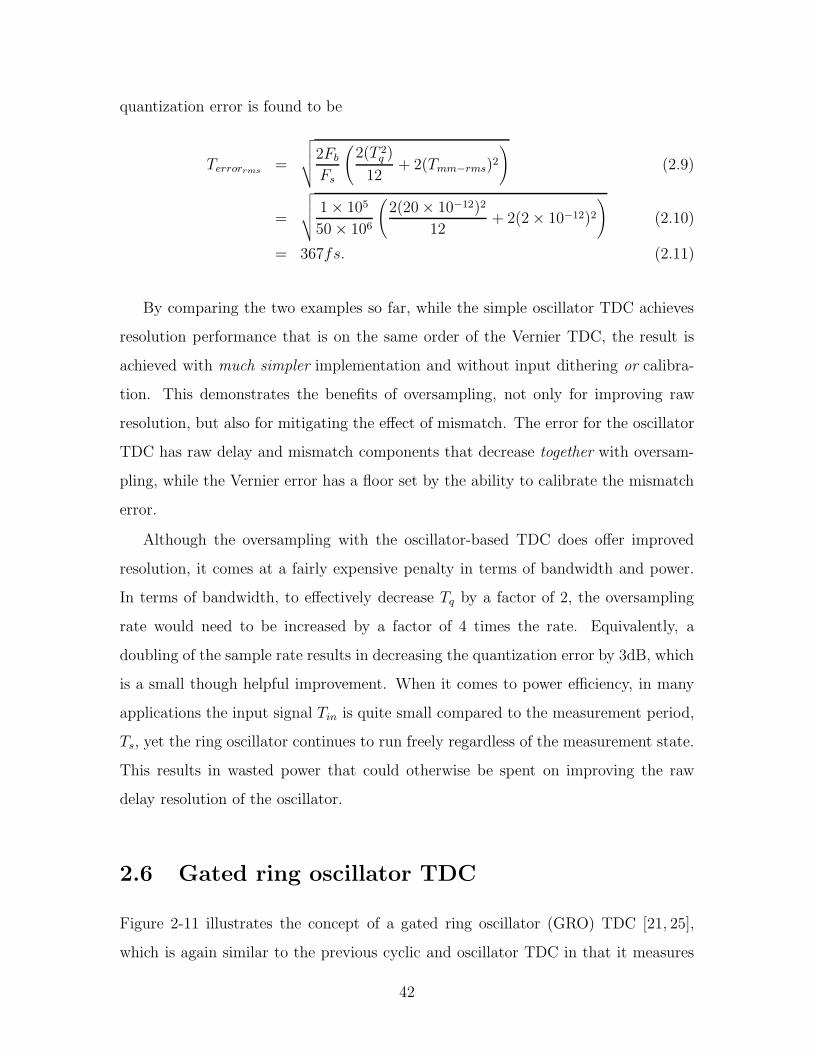
By comparing the two examples so far, while the simple oscillator TDC achieves
resolution performance that is on the same order of the Vernier TDC, the result is
achieved with much simpler implementation and without input dithering or calibra-
tion. This demonstrates the benefits of oversampling, not only for improving raw
resolution, but also for mitigating the effect of mismatch. The error for the oscillator
TDC has raw delay and mismatch components that decrease together with oversam-
pling, while the Vernier error has a floor set by the ability to calibrate the mismatch
error.
Although the oversampling with the oscillator-based TDC does offer improved
resolution, it comes at a fairly expensive penalty in terms of bandwidth and power.
In terms of bandwidth, to effectively decrease Tq by a factor of 2, the oversampling
rate would need to be increased by a factor of 4 times the rate. Equivalently, a
doubling of the sample rate results in decreasing the quantization error by 3dB, which
is a small though helpful improvement. When it comes to power efficiency, in many
applications the input signal Tin is quite small compared to the measurement period,
Ts, yet the ring oscillator continues to run freely regardless of the measurement state.
This results in wasted power that could otherwise be spent on improving the raw
delay resolution of the oscillator.
2.6 Gated ring oscillator TDC
Figure 2-11 illustrates the concept of a gated ring oscillator (GRO) TDC [21, 25],
which is again similar to the previous cyclic and oscillator TDC in that it measures
42

Gated RingOscillator
Register
Reset
Count
Out
Enable
Enable
OscillatorPhases
Count
MeasurementInterval Tin[k]
Out 6 7
Counters
qstart[k] qstart[k+1]
qstop[k-1] qstop[k]
qstart[k-1]
∆tq
Figure 2-11 Concept of the gated ring oscillator TDC
the number of delay element transitions during a measurement interval. Also similar
is the ability of the GRO-TDC to achieve large range with a small number of delay
elements. However, the key innovation in the gated ring oscillator is that instead of
enabling the counters during the measurement window, the ring oscillator itself is
gated with the Enable signal, with the state of the oscillator preserved in between
measurements.
By preserving the oscillator state at the end of the measurement interval Tin[k−1],
the quantization error Tstop[k − 1] from that measurement is also preserved. In fact,
when the following measurement of Tin[k] is initiated, the previous quantization error
is carried over as Tstart[k] = Tstop[k−1]. This results in first-order noise shaping of the
quantization error in the frequency domain, as evidenced by the first-order difference
operation on Tstop since the measurement error is given by
Terror[k] = Tstop[k] − Tstop[k − 1]. (2.12)
A subtle aspect to the GRO-TDC is that, along with the quantization noise,
the delay element mismatch is also first-order shaped. To see this more clearly,
let us examine the sequencing of delay elements for successive TDC conversions, as
43

Enable
Enable
Enable
Enable
Measurement 1
Measurement 2
Measurement 3
Measurement 4
Figure 2-12 Barrel-shifting of GRO delay elements to achieve first-order shaping of mis-match error
shown in Figure 2-12. What is clearly evident in this figure is that the selection of
delay elements for a given input is equivalent to the well-known barrel-shift algorithm
for dynamic element matching. Similar to the transfer of quantization error, the
mismatch errors for one sample are also passed along to and subtracted from the
following sample. Therefore, we can expect that in the case of oversampling, the GRO-
TDC architecture ideally achieves high resolution without the need for calibration,
even in the presence of large mismatch.
Now comparing the GRO-TDC to the oscillator-based TDC for a single-shot mea-
surement, the GRO-TDC will have the same additional quantization error penalty
found in Equation 2.1. However, when considering again the benefits from oversam-
pling, the GRO-TDC quantization error will ideally decrease by 9dB for a doubling
of the sample rate, which is a significant improvement compared to the 3dB possible
for the oscillator TDC. This relationship can be clearly seen in the expression for rms
TDC quantization error
Terrorrms=
√
√
√
√
(
Tq
2
)2 1
9π
(
2πFb
Fs
)3
(2.13)
44

An example GRO-TDC using the same parameters as the previous oscillator example
will then ideally have rms TDC quantization error of only
Terrorrms=
√
√
√
√
(
20 × 10−12
2
)21
9π
(
2π5 × 10⁴
50 × 106
)3
(2.14)
= 0.9fs! (2.15)
While this ideal performance level is far below typical thermal and 1/f noise levels
for digital CMOS, even the potential to achieve TDC resolution that is limited by
physical processes in a simple architecture is very compelling. The combination of
oversampling with first-order quantization noise and mismatch shaping is quite pow-
erful and can result in very high resolution conversion. Moreover, as will be seen in
the following sections, the GRO-TDC requires only a modest level of complexity that
can be implemented with small area and power consumption.
45

46

Chapter 3
Detailed GRO operation
3.1 Simple Gated Ring Oscillator Implementation
While first-order quantization noise shaping is very appealing for many applications,
it is yet unclear that preserving a ring oscillator state through the stop and start
operation is possible, and even more unclear is whether a simple circuit topology can
yield useful and practical results. Because the noise shaping we desire depends on
the accurate transfer of quantization error from one measurement to the next (i.e.
Tstart[k] = Tstop[k− 1]), it is important to consider how well this can be accomplished
with simple circuitry, and also how imprecise error transfer will affect noise-shaping.
Towards this end, we now consider a simple circuit topology to illustrate the key
design challenges of the gated ring oscillator.
3.1.1 GRO with inverter delay stages
Figure 3-1 illustrates one potential implementation for gating a ring oscillator by
using switches [21]. Starting from a classical inverter-based ring oscillator with an
odd number of stages, these switches are added in series to the positive and negative
power supply connections for each inverter, and all switches share a common state.
When the switches are closed, oscillation is enabled and the ring of inverters behaves
identically to a classical ring oscillator (Figure 3-1(a)). Conversely, when the switches
47

Enabled Ring Oscillator Disabled Ring Oscillator
(a) (b)
Figure 3-1 Conceptual implementation of gating a ring oscillator
Enable
Enable
Enable
VoiVoi-1
Delay Element
Vo4Vo1
Von
Vo2Vo3
Vo5
M4
M3
M2
M1
Von-1
Figure 3-2 Transistor-level schematic of a simple GRO
are open, the inverter delay element is unable to charge or discharge the parasitic
output capacitance, and as a result oscillation is suspended (Figure 3-1(b)). The
oscillator phase at the end of the enabled state is then held during the disabled state
with the charge stored on the parasitic capacitance of the delay elements.
The delay element switches of Figure 3-1 are well-suited for CMOS technology,
and can therefore be implemented for each element with complementary transistors
M1 and M4 as shown in Figure 3-2. For an odd number of stages, all of the NMOS
switches are controlled by an Enable signal, and likewise all of the PMOS switches
are controlled by an Enable signal (for simplicity, Enable will be used in reference to
the differential signals).
We should note that there are many ring oscillator configurations that can be
gated to hold phase information, including differential implementations. In fact,
48
differential delay elements are used in most TDC to achieve good differential non-
linearity performance, mitigating the mismatch between rising and falling edges. For
the GRO, however, the single-ended configuration shown in Figures 3-1 and 3-2 may
be preferable to a differential one. As explained earlier in Section 2.6, the error from
differential non-linearity is actually first-order shaped, and the single-ended topology
has half the power and area.
3.1.2 Model for skew due to oscillator gating
As mentioned earlier, perfectly preserving the GRO phase state is equivalent to setting
the initial quantization error Tstart[k] equal to the final error of the preceding sample,
Tstop[k − 1], and is required to achieve ideal noise-shaping. In a practical implemen-
tation, however, we can expect that the analog quantization error is not preserved
perfectly, and it is therefore important to understand the physical limitations as well
as the implications of practical quantization error transfer. With this goal in mind,
we begin by describing the issue of quantization error transfer in general terms, which
then will provide a context for evaluating specific GRO implementations.
When the output of a delay element is in transition, there are a number of dy-
namic mechanisms that determine the location and movement of charge within the
circuit. In Figure 3-3, for example, when the transition is interrupted by disabling the
oscillator, the dynamics of the transition are replaced by an entirely new and distinct
set of dynamics. For the interruption of a negative transition in Figure 3-3(a) or its
inverted positive transition in (b), the charge will redistribute to satisfy an equipo-
tential condition across the FET resistor that is left on, even in the disabled state.
Upon enabling the delay element once again, the transition resumes, however we can
see that the charge distribution within the cell is not the same as it was during the
original transition. Moreover, it is also clear that the amount of charge redistribution
depends on the state of the oscillator when Enable transitions low.
In addition to the charge redistribution within a delay element for transitioning
outputs, there is also some charge redistribution during the disable time for delay
elements that have an input in transition. As shown in Figure 3-4, both the switch
49

Enable
Vd
Vo
Vss
Vd
Vo
(a) (b)
Vo
Enable
Vo
Vdd
Cp
Cd
Cp
Cd
Rinv
Rinv
Rsw
Enable
Rsw
Vd
Vd
Figure 3-3 Conceptual picture of a transition being interrupted with a disable window.A negative transition is shown in (a), and the approximate inverse is shown in (b) for apositive transition.
drain voltages Vdpand Vdn
and the output voltage Voiwill be pulled towards the input
voltage Voi−1until the respective inverter core transistor turns off. Compared to the
case where the output is in transition, when the oscillator is enabled again most of
the redistributed charge here will quickly move back close to its original distribution
before the output begins to transition. While the charge redistribution for this case
is seen as secondary, it may also have a small effect on precise quantization error
transfer.
Since we now understand that the analog state information at the beginning of
a measurement interval is not strictly equal to the final state of the GRO from the
previous measurement, we now need to introduce this error in our mathematical
50

Vss
(a)
Voi
Cp
Cdn
Rswn
Enable
Vdn
Enable
Vdd
Cdp
Rswp
Vdp
Voi-1
Enable
Vdn
Voi-1
Vdp
Voi
Vdn
Voi-1
Vdp
Voi
(b)
Vdd
Vss
Vdd
Vss
Figure 3-4 Conceptual illustration of how charge redistribution within a delay elementdepends on the input level
model. To do this, for each measurement k we first define a variable θGRO[k] that
is equal to the GRO phase at the time when the negative Enable transition crosses
mid-supply. Second, we recognize that Tstart[k] will no longer be equal the value of
Tstop[k − 1], and we define another time error, Tskew that is a function of GRO phase
θGRO[k]. Tskew now models the corruption of the analog phase state as an unintended
consequence of gating the oscillator by the relation
Tstart[k] = Tstop[k − 1] + Tskew
(
θGRO[k])
. (3.1)
As another illustration of this additional error, Tskew, in Figure 3-5 we compare
the phase trajectory of an example GRO with its idealized piecewise linear phase
trajectory before and after the oscillator is disabled for a length of time, Tdisable.
Since it is not physically possible to gate an oscillator off and on instantaneously,
we can therefore expect a small amount of lag time, both when the GRO is disabled
and again when oscillation resumes. An equivalent way to define Tskew is to take the
difference between these two lag times, seen by extrapolating and subtracting the
tangential phase trajectories.
51
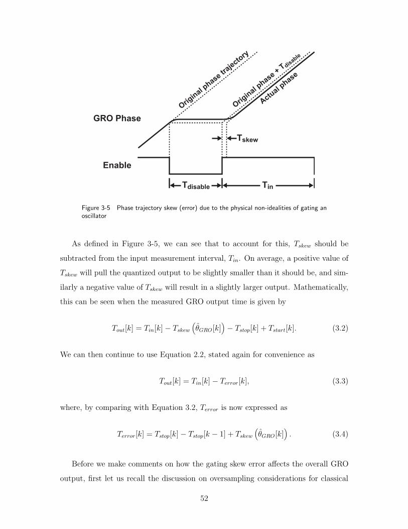
GRO Phase
Enable
Orig
inal p
hase traje
ctory
Orig
inal p
hase + Tdis
able
Actual p
hase
TinTdisable
Tskew
Figure 3-5 Phase trajectory skew (error) due to the physical non-idealities of gating anoscillator
As defined in Figure 3-5, we can see that to account for this, Tskew should be
subtracted from the input measurement interval, Tin. On average, a positive value of
Tskew will pull the quantized output to be slightly smaller than it should be, and sim-
ilarly a negative value of Tskew will result in a slightly larger output. Mathematically,
this can be seen when the measured GRO output time is given by
Tout[k] = Tin[k] − Tskew
(
θGRO[k])
− Tstop[k] + Tstart[k]. (3.2)
We can then continue to use Equation 2.2, stated again for convenience as
Tout[k] = Tin[k] − Terror[k], (3.3)
where, by comparing with Equation 3.2, Terror is now expressed as
Terror[k] = Tstop[k] − Tstop[k − 1] + Tskew
(
θGRO[k])
. (3.4)
Before we make comments on how the gating skew error affects the overall GRO
output, first let us recall the discussion on oversampling considerations for classical
52

quantizers from the previous chapter in Section 2.4. The applicable part of this
discussion is that the non-linear DC transfer characteristic of a classical quantizer
can be made to appear linear only if the quantization error is adequately scrambled.
Without scrambling, the output of the classical quantizer should be expected to be
non-linear, especially for inputs that are small or that create distinct quantization
patterns.
Because the gating skew error is also non-linear, adequately scrambling Tskew by
randomizing θGRO can also linearize the TDC behavior in the same manner that the
classical quantizer can be linearized. In this linear approximation, we can expect
that the GRO-TDC will have two non-physical noise profiles, a first-order noise-
shaped quantization error in addition to a white noise floor due to the skew error.
The required scrambling action can be accomplished by a combination of methods,
including random physical processes such as 1/f and thermal noise, intentional ran-
domization of the input signal through dithering, and pseudo-random patterns such
as the shuffling of delay element mismatch.
However, a lack of scrambling will leave the non-linearity to cause complex effects
in the quantizer output, especially when the converter is placed in a feedback system.
One example of these effects is the appearance of a deadzone in the quantizer DC
transfer characteristic, which will be discussed in Section 3.1.4. Generally avoiding
these effects is a very difficult challenge, and moreover the noise-shaping benefit of
the GRO-TDC architecture may be not be realized at all without a scrambled GRO
phase. Therefore, it is important to understand the root cause of this gating skew
error in more detail so that it may be minimized and appropriately scrambled by
design.
3.1.3 Gating skew analysis
With the framework for understanding skew already established, we now will turn
to identifying the mechanisms and variables that can affect Tskew by altering charge
within the delay cell. To this end, we begin with a cartoon of the gating skew for an
inverter-based GRO as shown in Figure 3-6. At the top of the figure, we see that the
53
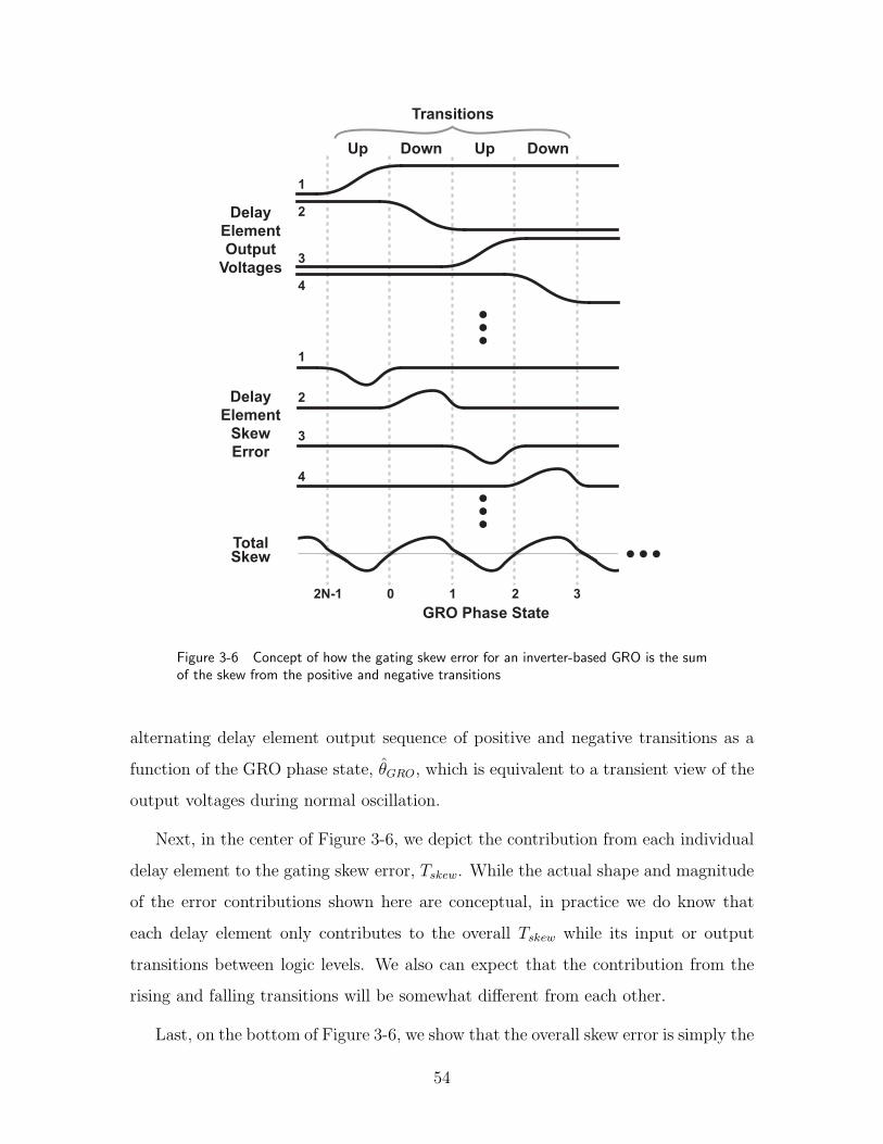
GRO Phase State
Delay
Element
Output
Voltages
2N-1 0 1 2
Delay
Element
Skew
Error
1
2
4
3
1
2
3
4
3
TotalSkew
Up Down Up Down
Transitions
Figure 3-6 Concept of how the gating skew error for an inverter-based GRO is the sumof the skew from the positive and negative transitions
alternating delay element output sequence of positive and negative transitions as a
function of the GRO phase state, θGRO, which is equivalent to a transient view of the
output voltages during normal oscillation.
Next, in the center of Figure 3-6, we depict the contribution from each individual
delay element to the gating skew error, Tskew. While the actual shape and magnitude
of the error contributions shown here are conceptual, in practice we do know that
each delay element only contributes to the overall Tskew while its input or output
transitions between logic levels. We also can expect that the contribution from the
rising and falling transitions will be somewhat different from each other.
Last, on the bottom of Figure 3-6, we show that the overall skew error is simply the
54

Enable
Enable
Output
Tdisable
Trise/fall
t = 0
Tθ
Output
toutput
Figure 3-7 Simulation testbench to characterize Tskew as a function of θGRO
combination of the individual contributions from each delay element, which reveals a
periodicity to the skew error of 2Tq due to the difference between the rising and falling
transitions, or alternately the difference between the NMOS and PMOS transistors.
For example, we can expect that since the PMOS switch transistors are twice as
large as the NMOS, the amount of charge injected from the PMOS will similarly be
twice the amount of charge injected from the NMOS. While we acknowledge that this
simplistic decomposition of GRO skew lacks precision, it does provide a backdrop for
understanding the complex features of the error.
To gain a more empirical view of gating skew for the inverter-based GRO, we
can simulate Tskew as a function of the GRO phase state θGRO at the transistor-
level in Spectre (SPICE) for a variety of conditions using the testbench shown in
Figure 3-7. For each curve, θGRO is swept by stepping Tθ, which successively moves
the falling edge of Enable across the GRO states. After a disable time Tdisable, the
oscillator is enabled again and allowed to reach steady-state. We then monitor the
time toutput at which a GRO delay element output transitions. Finally, the value of
Tskew is calculated from toutput by subtracting the disable time, and then comparing to
a reference time of toutput that is obtained from a simulation with no disable window.
The primary simulation parameters (excluding θGRO or Tθ) are the length of the
55

15
7.5
4.0
2.0
1.0
0.5
0.1
Disable
Width (ps)
0 0.5 1.0 1.5 2.0 2.5 3.0-0.4
-0.3
-0.2
-0.1
0
0.1N
orm
alized
Gati
ng
Skew
(Ts
ke
w / T
q)
GRO Disable Time Normalized to Tq
(Tθ / Tq = θGRO.47/π)
30
0.1ps
30ps
0 0.5 1.0 1.5 2.0 2.5 3.0-0.4
-0.3
-0.2
-0.1
0
0.1
2000
1000
500
250
125
60
30
Disable
Width (ps)
4000
30ps
4ns
GRO Disable Time Normalized to Tq
(Tθ / Tq = θGRO.47/π)
(a) (b)
Figure 3-8 Gating skew Tskew as a function of θGRO for stepped values of disable width(Tdisable) from (a) 0.1-30ps and (b) 30-4000ps. The Enable rise and fall times are heldconstant at 0.5ps.
disable time and the rise/fall times of the Enable signal. As shown in Figure 3-7,
Enable signals are constructed with piecewise linear voltage sources, and the length
of the disable time is taken from the 50% crossings of the supply. SPICE models for
a standard 0.13µm CMOS process with ideal matching are used throughout.
A first simulation to examine varies the width of the disable time with a very fast
rise/fall time that is held constant at 0.5ps, which is close to the ideal case of zero-
width rise and fall times but large enough to avoid convergence issues. Because many
charge transfer mechanisms occur with exponential time constants, the disable width
is stepped from 0.1 to 4000ps with approximately logarithmic increments. Figure 3-8
plots the results from this simulation, where (a) displays Tskew for short disable widths
of 0.1ps to 30ps, and (b) corresponds to the longer values of Tdisable, ranging from
30ps to 4,000ps.
By looking at these results, there are a few immediate observations on which to
comment. First, we can see in Figure 3-8(a) that as the disable width decreases, Tskew
limits to a zero-value, which is the same as the reference simulation with no disable
at all. Although this result is what intuition would suggest, it is satisfying to see that
the unrealistically fast Enable transients do not cause non-physical behavior in the
56

Enable
Vo
Enable
Vo
Vdd
(a) (b)
Cp
Cd
Cp
Cd
Rinv
Rinv
Figure 3-9 Schematic depicting two time constants present in the charge redistributionwithin a delay element whose output is in transition at the disable time
simulation. Second, we can verify that Tskew is indeed periodic with 2Tq, as predicted
by Figure 3-6. Last, as we can see clearly by the separation of Figure 3-8 into (a) and
(b), there are at least two time constants that dominate the motion of charge in the
inverter cell.
To explain the presence of more than one time constant, consider that when
the transition is interrupted, either the top or bottom of the inverter is open, with
the schematics for both cases drawn earlier in Figure 3-3, and shown here again for
convenience. When a GRO transition is disabled, the switch transistors turn off
and the charge in the switch transistor channels quickly diffuses, approximately half
moving to the supply and the other half into the inverter core. The capacitance at the
inverter drain, Cd, will at first absorb this charge injection at a rate determined by
the first time constant, and then eventually the voltage across Rinv will settle to zero
at a rate determined by the second time constant. Additional error with long time
constants may arise from delay elements with interrupted transitions at the input,
since these transistors are very weakly on and can have very large impedances.
Next, we know that the rise and fall times of Enable are practically much larger
than 0.5ps, which means that the turn-on time of transistors will depend on interac-
tion between the voltages within the GRO core and the voltages of Enable. We show
57
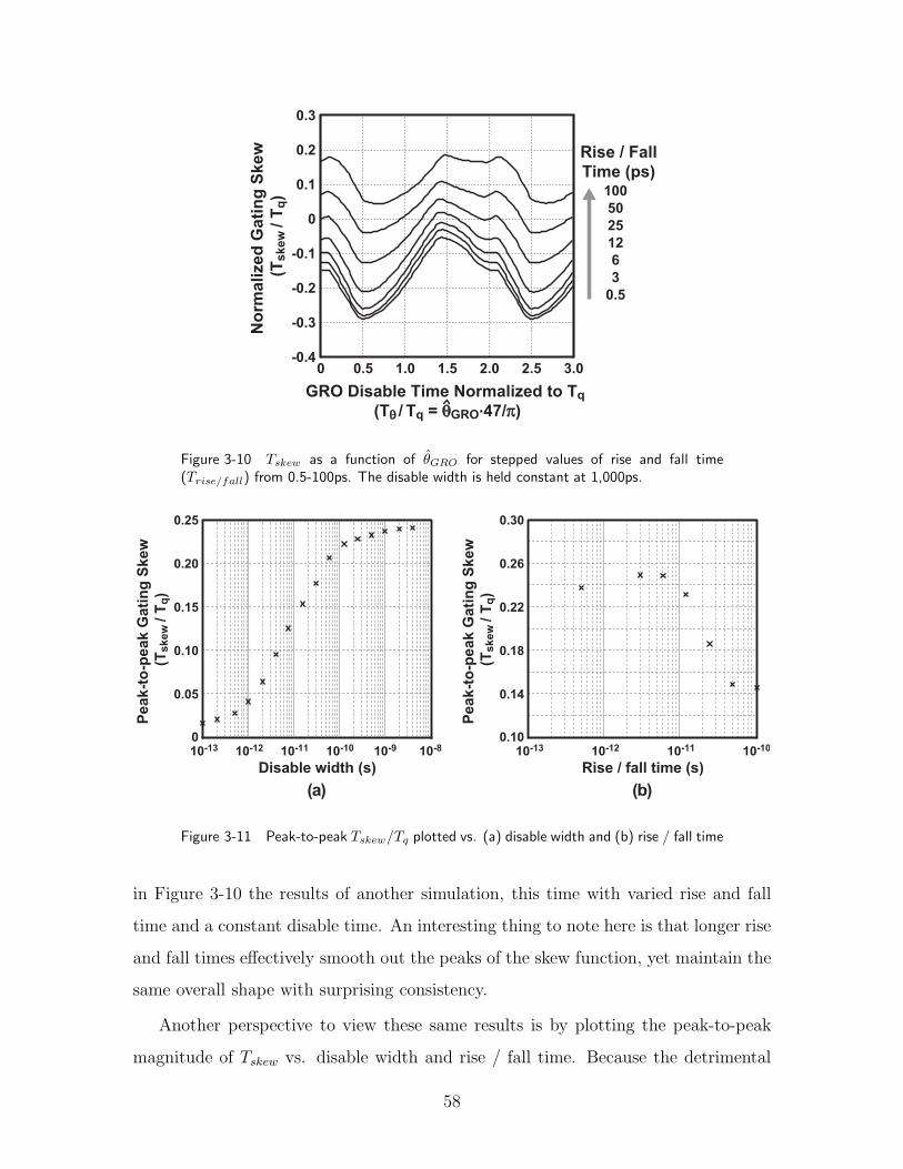
0 0.5 1.0 1.5 2.0 2.5 3.0-0.4
-0.3
-0.2
-0.1
0
0.1
0.2
0.3
No
rmalized
Gati
ng
Skew
(Ts
ke
w / T
q)
0.5
3
6
12
25
50
100
Rise / Fall
Time (ps)
GRO Disable Time Normalized to Tq
(Tθ / Tq = θGRO.47/π)
Figure 3-10 Tskew as a function of θGRO for stepped values of rise and fall time(Trise/fall) from 0.5-100ps. The disable width is held constant at 1,000ps.
10-130.10
0.14
0.18
0.22
0.26
0.30
(b)
Rise / fall time (s)10-12 10-11 10-10
Pe
ak
-to
-pe
ak
Ga
tin
g S
ke
w
(Tskew
/ T
q)
10-130
0.05
0.10
0.15
0.20
0.25
(a)
Disable width (s)
Pe
ak
-to
-pe
ak
Ga
tin
g S
ke
w
(Tskew
/ T
q)
10-12 10-11 10-810-10 10-9
Figure 3-11 Peak-to-peak Tskew/Tq plotted vs. (a) disable width and (b) rise / fall time
in Figure 3-10 the results of another simulation, this time with varied rise and fall
time and a constant disable time. An interesting thing to note here is that longer rise
and fall times effectively smooth out the peaks of the skew function, yet maintain the
same overall shape with surprising consistency.
Another perspective to view these same results is by plotting the peak-to-peak
magnitude of Tskew vs. disable width and rise / fall time. Because the detrimental
58

3.0 4.0 5.0
3.0
4.0
5.0
6.0
Normalized TDC input
Av
era
ge
d T
DC
ou
tpu
t
Simulated DC transfer characteristic
Figure 3-12 Simulated deadzones in the DC GRO-TDC transfer curve caused by gatingskew
effects of skew are caused by variation of Tskew with GRO phase, the DC offset is
irrelevant and can be removed. In Figure 3-11(a), we again can see the significant
changes in error magnitude for small disable widths, which have been explained al-
ready by the charge redistribution, and in (b) the slight decrease of Tskew with larger
rise / fall times can clearly be seen. Specifically, Tskew starts with a peak-to-peak
deviation of about 0.23Tq for fast rise / fall times, and then weakens to about 0.14Tq
for 100ps transitions. Thus, while a longer slope to Enable may be detrimental in
terms of jitter, in this case it actually contributes a small amount of ”averaging” that
could be seen as helpul in terms of gating skew error.
Due to the shallow slope of Tskew versus disable width for large values of Tdisable
seen in (a), we can say that in a standard 0.13µm CMOS process there is relatively
little charge lost to switch leakage. In deep sub-micron process technologies, however,
it is possible that subthreshold and gate leakage will present another source of error
that will change the shape and dependence of Tskew as a function of θGRO and Tdisable.
59

3.1.4 Deadzone effects
As mentioned earlier, many complex and interesting non-linear effects in the TDC
output can be caused by the gating skew error if the GRO phase is not scrambled
adequately. One important effect of the non-linear quantization error transfer is that
deadzones can be found in the GRO-TDC DC transfer characteristic. Since this is
a very standard measure for converter accuracy, it is worthwhile to understand this
issue in more detail.
As an example of this deadzone effect, Figure 3-12 plots a simulated DC transfer
characteristic using a behavioral model for the GRO-TDC. The MATLAB model is
based on Equation 3.2, where the value for Tskew comes from the Spectre simulation
results described earlier. For each data point, the MATLAB inputs a constant signal,
allows the GRO-TDC to reach steady-state, and then averages a large number of
repeated conversions.
To explain the deadzone behavior, we first consider that the non-linearity occurs
most prominently when the input to the converter is close to an integer multiple of
twice the delay Tin[k] − 2MTq = εT , where εT << Tq. Notice that in this case, the
quantization error at the end of a measurement interval is very close to the error at
the beginning of the interval. Mathematically we can see this as
Tstop[k] − Tstart[k] = εT . (3.5)
By substituting this into Equation 3.1, we also have that
Tstop[k] = Tstop[k − 1] + Tskew
(
θGRO[k])
− εT . (3.6)
In this expression, we can again see that the gating skew will push and pull the
GRO phase with a magnitude and direction determined by the phase of the previous
measurement. However, we can also see here that if the magnitude of Tskew is larger
than εT , then the influence of Tskew on the TDC output is also larger than it is for
εT . Recall that in the ideal GRO, where Tskew = 0 ∀ θGRO, even very small values of
60
εT will slowly accumulate over time and eventually cause the TDC output to change.
With the presence of a large, unwanted error that is a periodic function of the GRO
phase, the GRO will be pulled until a steady-state is reached. We can expect that
the gating skew error in a steady-state deadzone will be given by
Tskew(θGRO[k]) = εT . (3.7)
With this insight, a few comments can be made on the deadzones. Notice that in
Figure 3-12, the even integer values exhibit larger deadzones than the odd integers,
which is consistent with the periodicity of Tskew. However, if mismatch were to be
added, we would expect the period of Tskew to be equal to the GRO oscillation period,
2NTq. Therefore, practical deadzones are likely to be most severe when the GRO is
stopped on the exact same delay element transition for each measurement, which is
similar to injection-locking the GRO with the TDC sampling frequency. In this case,
we need to either provide a large amount of GRO phase scrambling, or reduce the
magnitude of Tskew far below that of random physical processes internal to the GRO.
3.1.5 Improving the gating sensitivity function
In this example GRO-TDC implementation, it is clear that the non-linearity due to
stopping and starting the oscillator can prevent the converter from fully realizing
the noise shaping that gives the architecture its advantages. Although the effective
TDC resolution has some benefit even from non-ideal noise shaping, at this point it
is still far from the physical noise limits of the architecture. To significantly improve
the effective TDC resolution to 1ps and below, we need a more sophisticated GRO
implementation than the example shown in Figure 3-2.
One approach to consider in reducing the effective non-linearity error, Tskew, would
be to provide random dithering of the TDC input as suggested earlier for deterministic
TDC in Section 2.4. Indeed, this technique would rid the TDC of deadzones by
scrambling the GRO phase, and also results in a “white” noise floor that is limited by
Tskew. Although oversampling could be now be used to filter noise outside the band of
61

interest, this approach moves away from the strength of the gated ring oscillator TDC,
namely the ability to inherently achieve noise-shaping of quantization and mismatch
errors with a simple architecture.
As an alternative to intentional dithering, we can consider optimum sizing of
transistors within the inverter delay cell to reduce the magnitude of Tskew within the
inverter-based GRO architecture of Figure 3-2. However, this approach can improve
the raw magnitude of Tskew by only a small amount, and even this small improvement
is not robust across processes, power supply voltages, etc.
Finally, let us consider the approach to reduce the magnitude of Tskew through
interpolation or averaging. We have seen in Figure 3-6 that the gating skew is com-
posed of contributions from alternating positive and negative transitions. If multiple
skew contributions can be averaged together, then it may be possible to scale both
the gating skew as well as the effective oscillator delay, Tq. Therefore, we proceed
to consider architectural modifications to the GRO of Figure 3-2 that can achieve
sub-gate-delay raw resolution.
3.2 Multi-Path Gated Ring Oscillator
In this section, we first explore the suitability of various sub-gate-delay ring oscillator
topologies for implementing a gated ring oscillator. We then identify the most promis-
ing of these architectures to be the multi-path oscillator, and follow with a detailed
analysis, considering especially the critical architectural issues and tradeoffs for use
as a gated ring oscillator. Next, we present a design methodology and circuit details
for use within a prototype GRO-TDC, and then revisit the issue of quantization error
transfer accuracy, or gating skew. We demonstrate through simulations the marked
improvements in gating skew error using the proposed multi-path oscillator compared
to the simpler inverter topology discussed previously in Section 3.1.3, and provide a
physical explanation for the improved skew performance.
62

Z2
Enable
Enable
Z3 Z4 Z5 Z6 Z7 Z8
Z2
Z3
Z4
Z5
Z6
Z7
Phase stateis lost
Figure 3-13 Illustration of the problem in using resistive interpolation for the GRO
3.2.1 Achieving sub-gate-delay raw resolution
Earlier in Section 2.3, a few techniques for creating sub-gate-delay TDC resolution
were discussed. Due to geometric similarities, the approaches commonly used in cyclic
TDC are of particular interest for application to the GRO. For example, it is natural
to consider the interpolating technique implemented either with rings of resistors or
with transistors. In addition to oscillators within the TDC community, research in
precisely generating multi-phase signals for fixed-frequency phase and delay-locked
loop applications have also investigated similar ideas that can be considered for the
GRO [11,12, 16, 31, 35, 36, 38, 42, 63].
The resistor ring often used in multi-phase oscillator applications is able to gener-
ate very high-resolution and low differential non-linearity, however we can quickly see
that this particular topology has fundamental problems for the gated ring oscillator.
To explain, Figure 3-13 applies the concept of resistive interpolation to the gated ring
oscillator, with the assumption that a differential delay element structure would be
used in practice. Although the power and area penalty of the differential structure
can be tolerated for the GRO (as discussed earlier in Section 3.1.1), the main issue
here is that when the GRO is disabled, current will continue to flow in the resistor
63
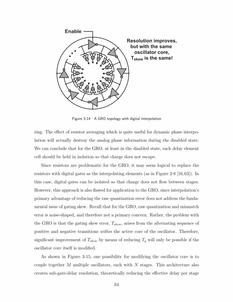
Enable
Resolution improves,but with the same
oscillator core,Tskew is the same!
Figure 3-14 A GRO topology with digital interpolation
ring. The effect of resistor averaging which is quite useful for dynamic phase interpo-
lation will actually destroy the analog phase information during the disabled state.
We can conclude that for the GRO, at least in the disabled state, each delay element
cell should be held in isolation so that charge does not escape.
Since resistors are problematic for the GRO, it may seem logical to replace the
resistors with digital gates as the interpolating elements (as in Figure 2-8 [16,63]). In
this case, digital gates can be isolated so that charge does not flow between stages.
However, this approach is also flawed for application to the GRO, since interpolation’s
primary advantage of reducing the raw quantization error does not address the funda-
mental issue of gating skew. Recall that for the GRO, raw quantization and mismatch
error is noise-shaped, and therefore not a primary concern. Rather, the problem with
the GRO is that the gating skew error, Tskew, arises from the alternating sequence of
positive and negative transitions within the active core of the oscillator. Therefore,
significant improvement of Tskew by means of reducing Tq will only be possible if the
oscillator core itself is modified.
As shown in Figure 3-15, one possibility for modifying the oscillator core is to
couple together M multiple oscillators, each with N stages. This architecture also
creates sub-gate-delay resolution, theoretically reducing the effective delay per stage
64
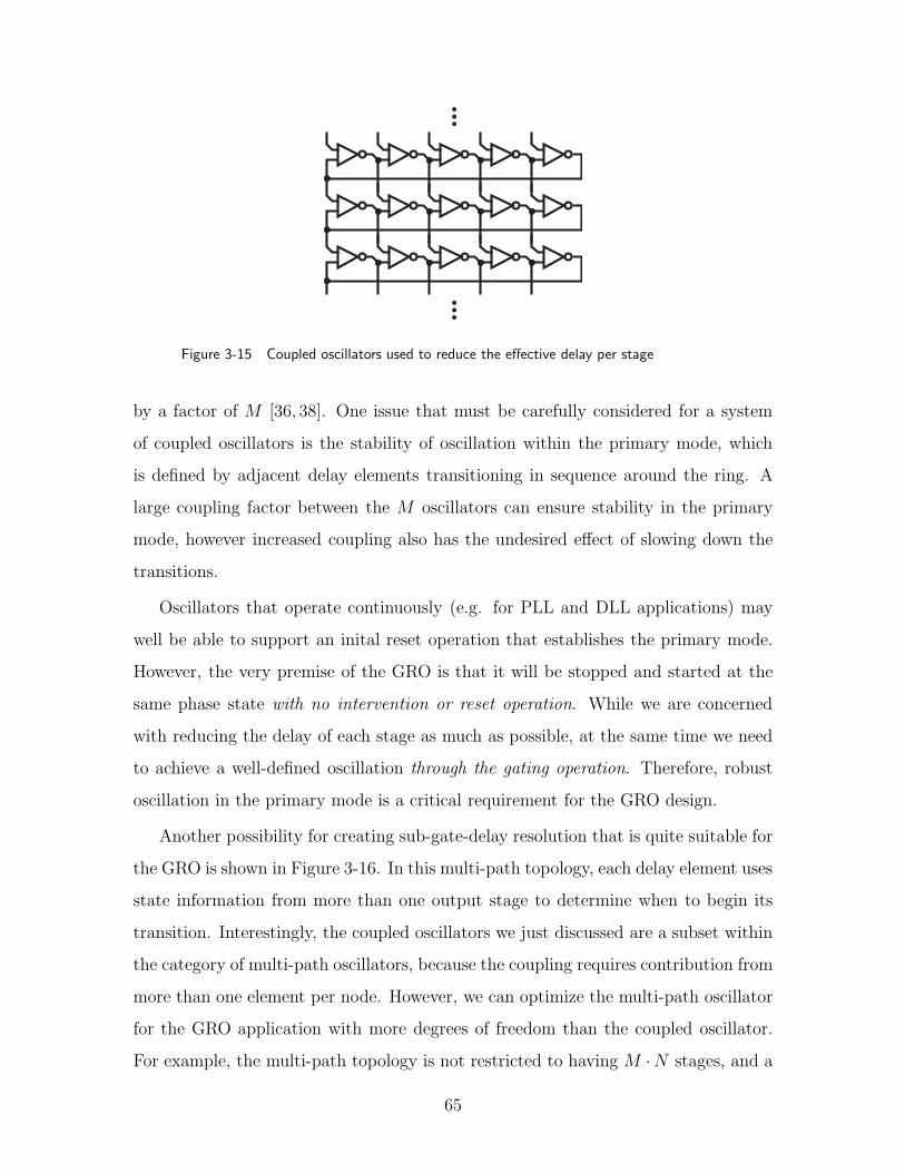
Figure 3-15 Coupled oscillators used to reduce the effective delay per stage
by a factor of M [36, 38]. One issue that must be carefully considered for a system
of coupled oscillators is the stability of oscillation within the primary mode, which
is defined by adjacent delay elements transitioning in sequence around the ring. A
large coupling factor between the M oscillators can ensure stability in the primary
mode, however increased coupling also has the undesired effect of slowing down the
transitions.
Oscillators that operate continuously (e.g. for PLL and DLL applications) may
well be able to support an inital reset operation that establishes the primary mode.
However, the very premise of the GRO is that it will be stopped and started at the
same phase state with no intervention or reset operation. While we are concerned
with reducing the delay of each stage as much as possible, at the same time we need
to achieve a well-defined oscillation through the gating operation. Therefore, robust
oscillation in the primary mode is a critical requirement for the GRO design.
Another possibility for creating sub-gate-delay resolution that is quite suitable for
the GRO is shown in Figure 3-16. In this multi-path topology, each delay element uses
state information from more than one output stage to determine when to begin its
transition. Interestingly, the coupled oscillators we just discussed are a subset within
the category of multi-path oscillators, because the coupling requires contribution from
more than one element per node. However, we can optimize the multi-path oscillator
for the GRO application with more degrees of freedom than the coupled oscillator.
For example, the multi-path topology is not restricted to having M ·N stages, and a
65

Single InputSingle Output
Multiple InputsSingle Output
Figure 3-16 Basic concept of using multiple inputs for each delay stage
(c) Unrestricted connections
(b) Multiple skewed inverters
(a) Asymmetrically skewed inverter
Voi
Voi-j2
Voi-j1
Voi-j4
Voi-j3
Voi-jK
Voi-jK-1
Voi
Voi-j1Voi-j2Voi-jK
Voi
Voi-j
Voi-1
Figure 3-17 Techniques to reduce effective delay by modifying the standard inverter
primary oscillation mode can more easily be established.
One example of this multi-path topology is to modify the standard two-transistor
inverter delay cell by asymmetrically connecting the PMOS and NMOS inputs to
different delay stage outputs [35]. With the transistor drains both connected to the
66
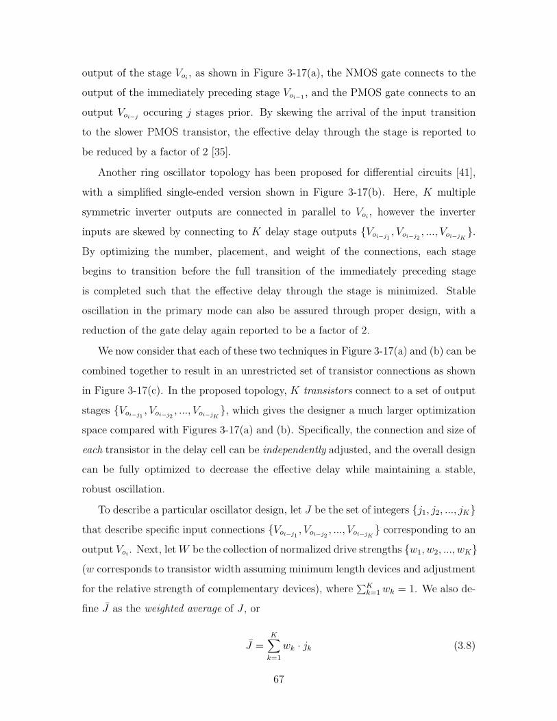
output of the stage Voi, as shown in Figure 3-17(a), the NMOS gate connects to the
output of the immediately preceding stage Voi−1, and the PMOS gate connects to an
output Voi−joccuring j stages prior. By skewing the arrival of the input transition
to the slower PMOS transistor, the effective delay through the stage is reported to
be reduced by a factor of 2 [35].
Another ring oscillator topology has been proposed for differential circuits [41],
with a simplified single-ended version shown in Figure 3-17(b). Here, K multiple
symmetric inverter outputs are connected in parallel to Voi, however the inverter
inputs are skewed by connecting to K delay stage outputs Voi−j1, Voi−j2
, ..., Voi−jK.
By optimizing the number, placement, and weight of the connections, each stage
begins to transition before the full transition of the immediately preceding stage
is completed such that the effective delay through the stage is minimized. Stable
oscillation in the primary mode can also be assured through proper design, with a
reduction of the gate delay again reported to be a factor of 2.
We now consider that each of these two techniques in Figure 3-17(a) and (b) can be
combined together to result in an unrestricted set of transistor connections as shown
in Figure 3-17(c). In the proposed topology, K transistors connect to a set of output
stages Voi−j1, Voi−j2
, ..., Voi−jK, which gives the designer a much larger optimization
space compared with Figures 3-17(a) and (b). Specifically, the connection and size of
each transistor in the delay cell can be independently adjusted, and the overall design
can be fully optimized to decrease the effective delay while maintaining a stable,
robust oscillation.
To describe a particular oscillator design, let J be the set of integers j1, j2, ..., jK
that describe specific input connections Voi−j1, Voi−j2
, ..., Voi−jK corresponding to an
output Voi. Next, let W be the collection of normalized drive strengths w1, w2, ..., wK
(w corresponds to transistor width assuming minimum length devices and adjustment
for the relative strength of complementary devices), where∑K
k=1 wk = 1. We also de-
fine J as the weighted average of J , or
J =K∑
k=1
wk · jk (3.8)
67

To make use of these definitions, we first consider a standard ring oscillator with
J = 1. Not coincidentally, we find that the oscillation period is equal to Tosc =
2NTinv/J . Here Tinv is the delay of a standard inverter, and N is the number of
stages. While this is convenient for the case of the standard inverter ring, to be
more general we say that Jeff is the effective weighted average of J , defined when the
period for any ring oscillator is given by
Tosc =2NTinv
Jeff(3.9)
To continue, we next can consider a multi-path ring oscillator with accelerated tran-
sistions that reduces the oscillation period to Tosc = 2NTq. By combining with
Equation 3.9, we have
Tq =Tinv
Jeff
. (3.10)
From this result, the designer may be tempted to reduce Tq by increasing Jeff as
much as possible, however, there are a number of practical considerations that limit
its attainable value. First, consider that only connections to the previous (N − 1)/2
stages are useful for primary mode oscillation, and a more practical rule is to restrict
J to a maximum of N/3. Therefore, achieving a large value of Jeff requires a large
number of stages, which in turn requires larger area.
Second, we need to consider the stability of the oscillator. If J is large, and/or
concentrated heavily at N/3 without a distributed contribution over the entire range
of J , secondary oscillation modes become difficult to suppress, especially in the pres-
ence of mismatch. While using a prime number of stages can be helpful in this regard,
a conservative design should have at least one input connection with some weight for
every 4 stages to ensure that transitions occur in the proper sequence. We will later
see that this strategy is also helpful in reducing the gating skew.
Finally, the larger values in J will typically add more parasitic wiring capacitance
to the delay element output, since these elements need to be placed further away.
Moreover, the parasitic capacitance will also become more important when multiple
connections with small weights are chosen. We then introduce η, an efficiency factor
68

Eff
icie
ncy F
acto
r an
d
Eff
ecti
ve D
ela
y
(η a
nd
Tq/T
inv)
0
1
Weighted Average of
Delay Element Connections
(Σ wk.jk)
η
Tq/Tinv
Efficiency
decreases
1
AggressiveConservative
Effective
delay
decreasesSweet
spot
Figure 3-18 Example tradespace for optimizing the resolution of a multi-path oscillatoroperating in its primary mode by considering the weighted average of J
that takes into consideration switching transients and wiring parasitics to result in
Jeff = ηJ = ηK∑
k=1
wk · jk. (3.11)
As an example tradespace shows in Figure 3-18, an optimal design in terms of resolu-
tion should not just consider the weighted average of J , but also its product with η.
Fortunately, in general this efficiency factor degrades smoothly, and can be estimated
by including including crude parasitic wiring capacitance models in the transistor-
level simulations.
3.2.2 Design of the Proposed Multi-Path GRO
The delay cell from Figure 3-17(c) can be easily modified to accomodate the gat-
ing functionality by again placing appropriate switches above and below the inverter
core as shown in Figure 3-19. In the same manner as was described earlier in Sec-
ton 3.1.1, all impedances are high in magnitude during the disabled state, which will
approximately preserve the oscillator state in between measurements.
With the delay cell building block now defined, let us consider the number of stages
69

Voi
Voi-j2
Enable
Enable
Voi-j1
Voi-j4
Voi-j3
Voi-jK
Voi-jK-1
Figure 3-19 Delay cell topology for the proposed gated ring oscillator
N that is appropriate for use in the GRO-TDC application. Counting and measuring
the GRO outputs with standard digital logic places an upper bound on the oscillation
frequency of 2GHz, which is a period conservatively equal to ten inverter delays in
the 0.13µm CMOS process. For a minimum design goal of Jeff ≈ 5, this implies that
the number of stages N ≈ 50. An upper bound on N is less strict, and is determined
primarily by practical limitations such as the number of connections per stage and
silicon area (for the same set J = j1...jK, a larger N does not reduce Tq). Another
issue for choosing N is that a prime value inherently has better rejection of undesirable
modes than does a value of N with large odd factors, such as 45 = 3 · 15 = 5 · 9. As
a result of these considerations, we propose here that N = 47.
To set the delay cell transistor connections and sizes, we use a soft approach
based on empirical simulation results in combination with the desire to minimize
layout complexity and area. A useful metric for evaluating designs is the power-delay
product, which can achieve a local minimum for a well-designed multi-path oscillator.
Another useful indicator of stability, albeit somewhat qualitative, is the steady-state
start-up time of the oscillator when given a minor charge injection onto one of the
oscillator nodes.
Although simulation is used for final assignment of connections and weights, there
are a number of guidelines that are also useful to generate a first-pass design that
70

Enable
Vo46
Vo47
Vo2
Vo1
Vo43
Vo44
Enable
Vo37
Vo1
Vo35
Vo47Vo43Vo39
0.6µ1.2µ1.2µ
2.0µW = 3.0µ
Vo45
Vo47
Vo1
Vo43
Vo39
Vo37
Vo35
Delay Stage #1
Enable
Figure 3-20 Schematic of the proposed multi-path GRO
is relatively close to optimal. As discussed earlier in regard to Figure 3-17(a), con-
necting the slower PMOS transistors to the largest values in J results in a better
efficiency. Depicted in Figure 3-20, the PMOS connections are then made to the
13th and 11th preceding stages Voi−13, Voi−11, while NMOS connections are made
to Voi−9, Voi−5, Voi−1. Whereas the PMOS connections establish the maximum value
of J close to N/3, the NMOS connections are distributed to efficiently establish the
fundamental oscillation mode with minimal penalty in speed.
In terms of sizing, a larger weight is assigned to the connections with longest
distance, with only a small drive from the immediately preceding stage. To facilitate
a compact and simple layout as shown in Figure 3-21, the same number of equal-width
fingers (5) is used for each of the four levels in the transistor stack (PMOS switch,
PMOS inverter, NMOS inverter, NMOS switch). For optimal power and speed, the
switch transistors are sized wider than the total width of the inverter core transistors.
A summary of J and W is given in Table 3.1.
71
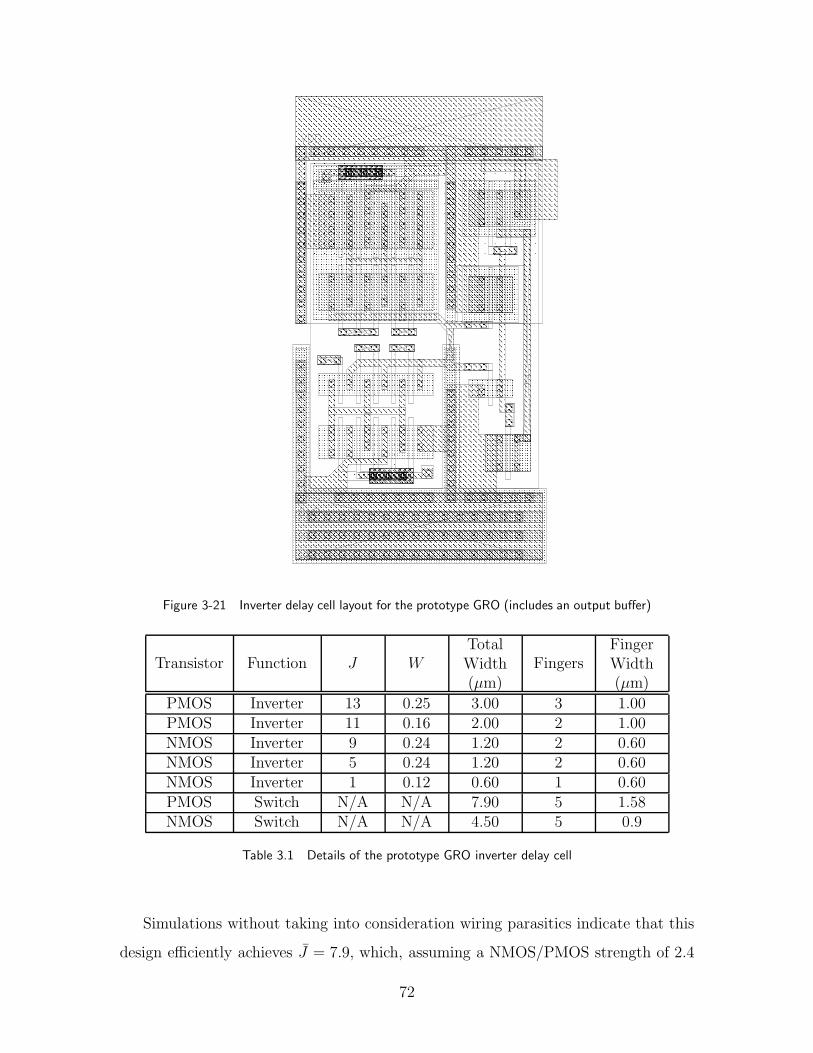
11111111111111111111111111111111111111111111111111
1111111111111111111111111111111111111111111111111111
1111111111
1111111111111111111111111111111111111111111111111111
11111111111111111111111111111111111111111111111111111111111111111111111111111111111111111111111
1111111111111111111111111111111111111111111111111111
111111
11111111111111111111111111111111111111111111111111
1111111111111111111111111111111111111111111111111111111111111111111111111111111111111111
111111111111111
11111111111111111111111111111111111
11111111111111111111111111111111111111111111111111
11111111111111111111111111111111111111
11111111111111111111111111111111111111111111111111
1111111111
1111111111111111
1111111111111111
1111111111111111111111111111111111111111111111
1111111111111111111111111111111111111111111111
1111111111111111111111111111111111111111111111
1111111111111111111111111111
11111111111111111111111111111111
111111111111111111111111111111
111111111111111111111111
11111111111111111111111111
1111111111111111111111
11111111111111111111
111111111111
111111111111
11111111111111111111
111111111111
111111111111
1111111111111111111111111111111111111111111111111111111111111111111111111111111111111111111111111111111111111111111111111111111111111111111111111111111111111111111111111111111111111111111111111111111111111111111111111111111111111111111111111111111111111111111111111111111111111111111111111111111111111111111111111111111111111111111111111111111111111111111111111111111111111111111111111111111111111111111111111111111111111111111111111111111111111111111111111111111111111111111
11111111111111111111111111111111111111111111111111111111
1111111111111111111111111111111111111111
111
1111111111111111111111
11111111
11111111111111111111111111111111
1111111111
111111111111111111111111
11111111
111111111111111111111111111111111111111111111111111111111111111
11111111
111111111111111111111111111111111111111111111111111111111111111111111111111111111111111111
111111
11111111
111
11111111111111
111111
11
111111
11
111111
111111111111111111111111111111111111111
111111111111111111111111111111111111111111111111111111111111111
111111111111111111111111111111111111111111111111111111111111111111111111111111111111111111111111111111111111111111111111111111111111111111111111111111111111111111111111111111111111111111111111111111111111111111111111111111111111111111111111111111111111111111111111111111111111111111111111111111111111111111111111111111111111111111111111111111111111111111111111111111111111111111111111111111111111111111111111111111111111111111111111111111111111111111111111111111111111111111111111111111111111111111111111111111111111111111111111111111111111111111111111111111111111111111111111111111111111111111
111111111111111111111111111111111111111111111111111111111111111111111111111111111111111111111111111111111111111111111111111111111111111111111111111111111111111111111111111111111111111111111111111
111111111111111111111111111111111111111111
111111
111111
1111
1111
1111
111
11
11
1111
11
11
1111
11
11111111
1111
1
11
1
11
11
11
11
1
1111
11
1111
1
11
1111
1
11
111111
11
1111
11
1111
1111
11
11
1111
1111
1111
1111
11
11
1111
11
1111
11
1111
11
11
1111
1
1111
1111
111111
11
11
1111
11
11
11
11
1111
1111
1111
11
1111
1111
1111
1
11
1
11
1111
11
1111
11
11111111111111
1111111
11
111111
111111
11111111
1111111111
111111
1111
11
1111
11
111111
111111
11111111
1111111111
111111
1111
11
1111
11
111111
111111
11111111
1111111111
111111
1111
11
1111
11
1111
1111
1111
1111
11
1111
11
1111
11
1111
1111
1111
1111
11
1111
11
1111
11
111111111111111111111111111111
111111111111111111111111
1111111111
11111111
111111
11
11111111111
111111
111
11
1
1111
11
11
1
11
1
111111111111111111
111111111111111111111111111111111111111111111111111111111111111
11111111111111
111111111111
11111111111111
111111111111111111
1111111111111111
111111111111111111111111111111111111
1111
111111
111111
11111111
111
1111
1111111
111111111111111111111111111111111111111111111111111111111111
111111111111111111111111111111111111111111111111111111111111111
1111111111
11111111111111
111111
11111111
111111111111111111111111111111111111111111111111111
111
1111111111
1111111111111111111111
1111
111111
111111111111111111111111111111111111111111111111111111111111111111111111111111111111111111111111111
11111111
1111111111111111111111
11
1111111111
111111111111111111111111111111111111111111111
111111111111111111
1111111111111111
1111111111111111111111111111111111111111111111111111111111111111111111111111111111111111111111111111111111111111111111111111111111111111111111111111111111111111111111111111111
1111111111111111111111111111111111111111111111111111111111111111111111111111111111111
11111111111
11111111111111111111111111111111
11111111111111111111111111111111111111111111111111111111111111111111111111111111111111111111111111111111111111111111111111111111111111111111111111111111111111111111111111111111111111111111111111111111
111111111111111111111111111111111111111111111111111111111111111111111111
111111111111111111111111
1111111111111111111111
1111111111
1111111111
11111111111111
11111111111111
11111111111111111111111111111111111111111111
11111111111111111111111111111111111111111111
11111111111111111111111111111111111111111111
1111111111111111111111111111
111111111111111111111111111111
111111111111111111111111111111
111111111111111111111111
11111111111111111111111111
11111111111111111111
111111
11111111
1111
11111111
1111
1111
1111
1111
11
1111
11
1111
1111111111
1111111111111111
1111111111
11111111
11
111111
1111
11111111
1111111111111111111111
1111111111
111111
111111
1111
111111
111111111111
1111111111
Figure 3-21 Inverter delay cell layout for the prototype GRO (includes an output buffer)
Transistor Function J WTotalWidth(µm)
FingersFingerWidth(µm)
PMOS Inverter 13 0.25 3.00 3 1.00PMOS Inverter 11 0.16 2.00 2 1.00NMOS Inverter 9 0.24 1.20 2 0.60NMOS Inverter 5 0.24 1.20 2 0.60NMOS Inverter 1 0.12 0.60 1 0.60PMOS Switch N/A N/A 7.90 5 1.58NMOS Switch N/A N/A 4.50 5 0.9
Table 3.1 Details of the prototype GRO inverter delay cell
Simulations without taking into consideration wiring parasitics indicate that this
design efficiently achieves J = 7.9, which, assuming a NMOS/PMOS strength of 2.4
72

44 43
45 46
X 47
1 2
42 39
41 40
4 5
3 6
38 35
37 36
8 9
7 10
34 31
33 32
12 13
11 14
30 27
29 28
16 17
15 18
26 25
23 24
22 21
19 20
Figure 3-22 Delay cell layout floorplan for the prototype multi-path GRO
is in line with the ideal calculation of
J = 13 · 0.25 + 11 · 0.16 + 9 · 0.24 + 5 · 0.24 + 1 · 0.12 = 8.4. (3.12)
To include the parasitics, we can estimate η equal to 0.5-0.7, which results in a value
of Jeff = 4-6. Compared with the prior work on multi-path oscillator architectures
discussed earlier with Jeff = 2, this is roughly a factor of 2-3 improvement. The
expected performance is confirmed with measurement results, which are discussed in
Chapter 5.
To minimize mismatch both in the delay elements and in the routing parasitic ca-
pacitance, a serpentine arrangement of delay elements within was used in the layout,
as shown in Figure 3-22. However, the routing was done by hand in a single pass, em-
ploying no special techniques to equalize the routing lengths or parasitic capacitances
of each delay element output.
3.2.3 Non-linearity of the Proposed Multi-Path GRO
With the raw resolution of the TDC much improved with the multi-path architecture,
we can now revisit the issue of reducing the magnitude of the quantization error
73

Time
Vo
lta
ge
Figure 3-23 Simulated transient voltages of the multi-path delay element outputs
transfer non-linearity. Recall the hypothesis from before that the magnitude of Tskew
can be reduced by averaging the skew contributions from multiple elements that are
in transition at the same time. To get a sense of how the different transitions relate
to each other in the proposed multi-path GRO design, Figure 3-23 plots all of the
transient voltages on the same time axis. If we look closely at this figure and carefully
count the number of transitions active at any given time, we should not be surprised
to find about 13 overlapping transitions, since 13 is the maximum value of J for this
particular multi-path design.
With this picture in mind, we can then revise the cartoon depicting gating skew
error for the multi-path architecture as shown in Figure 3-24. At the top of the figure,
the alternating pattern of positive and negative transitions vs. GRO phase state are
the same waveforms as in Figure 3-23, except that here each delay element output is
presented individually. We also see that defining the GRO phase state is much more
ambiguous, which is an issue that is later discussed in more detail in Chapter 4.
Because the transitions of the multi-path oscillator delay elements are much wider
with respect to Tq than before, we can also expect that the gating skew contribution
from each transition will be much wider as well. In the center of Figure 3-24, we
now depict a gating skew error with the same conceptual shape and magnitude as
74
GRO Phase State
Transition Width
Spans Entire Range
of Input Connections
Delay
Element
Output
Voltages
10 15
Delay
Element
Skew
Error
17
18
20
19
17
18
19
20
20 25
TotalSkew
Figure 3-24 Concept of how the overlapping skew from positive and negative transitionsfor a multi-path GRO significantly reduces the total skew
before in Figure 3-6, although here the width of the contribution has effectively been
stretched over a span of 13Tq. Depicting the individual error contribution in this
way is a physically intuitive and reasonable thing to do, since we have already seen
that charge redistribution is the primary mechanism for skew error, and also that
any delay element in transition will observe some amount of charge redistribution.
In addition, the equivalent circuit schematic for each individual delay element during
the disable window has not significantly changed from the schematic shown earlier in
Figure 3-9.
Finally, we show at the bottom of Figure 3-24 that the overall skew error is the
“average” of the individual contributions from each delay element, with the result
75
being much smaller than any of the individual contributions. To consider how this
“averaging” relates to the physical oscillator, recall that the delay elements in a multi-
path oscillator are strongly coupled together. Thus, when a charge is unnaturally
injected into one of the transitioning delay elements, its influence will be mitigated
by the inertia of the other delay elements, since all of the elements must work together
in converging to a single phase state. This physical analogy provides some justification
for depicting the total skew as an “average” of individual contributions that we will
later verify through simulation and measurements.
Although Figure 3-24 demonstrates that summing the overlapping transition skew
contributions from many stages will result in a smoother skew function with decreased
variation, it is not clear how much improvement we can expect. In fact, the amount
of reduced variation that results from “averaging” multiple functions in this manner
strongly depends on the specific characteristics of the individual functions, as well as
the time offset that separates them. In addition, we have so far approximated the
oscillator state space with only two-dimensions (phase and time), which provides a
useful, albeit crude, tool for understanding the relevant issues of gating skew, but
does not model the complex intricacies within the GRO. Therefore, we again turn to
a simulation testbench similar to that in Figure 3-7 to gain a more quantitative sense
of the improved variation of Tskew in the multi-path GRO.
Figure 3-25 displays a single simulated curve for the proposed multi-path GRO
Tskew as a function of θGRO, assuming typical operating conditions of a 1ns disable
width and 50ps rise / fall times, and also with the DC component of Tskew removed for
clarity. While the smooth, near sinusoidal shape and period of 2Tq are as expected,
the aspect of this figure that is striking is the very small magnitude of the error.
Compared to the gating skew error simulated for the inverter-based GRO, the peak-
to-peak magnitude shown here is almost an order of magnitude smaller, and this result
is with respect to Tq. Thus when the reduction of Tq is also considered so that the
gating skew error is seen in units of time, the simulated peak-to-peak variation of the
proposed multi-path oscillator is smaller than the inverter-based GRO by significantly
more than a factor of 10.
76

0 1.0 2.0 3.0 4.0
No
rmalized
Gati
ng
Skew
(Ts
ke
w / T
q)
GRO Disable Time Normalized to Tq
(Tθ / Tq = θGRO.47/π)
0.010
0.015
0.000
0.005
-0.010
-0.005
-0.015
Figure 3-25 Multi-path GRO Tskew as a function of θGRO for typical conditions with adisable width of 1ns, and a rise / fall time of 50ps
15
7.5
4.0
2.0
1.0
0.5
0.1
Disable
Width (ps)
0 0.5 1.0 1.5 2.0 2.5 3.0
No
rmalized
Gati
ng
Skew
(Ts
ke
w / T
q)
GRO Disable Time Normalized to Tq
(Tθ / Tq = θGRO.47/π)
30
0.1ps
30ps
0 0.5 1.0 1.5 2.0 2.5 3.0
2000
1000
500
250
125
60
30
Disable
Width (ps)
4000
30ps
4ns
GRO Disable Time Normalized to Tq
(Tθ / Tq = θGRO.47/π)
(a) (b)
-1.6
-1.2
-0.8
-0.4
0
-1.6
-1.2
-0.8
-0.4
0
Figure 3-26 Multi-path GRO gating skew Tskew as a function of θGRO for stepped valuesof disable width (Tdisable) from (a) 0.1-30ps and (b) 30-4000ps. The Enable rise andfall times are held constant at 0.5ps.
To compare the multi-path GRO topology with the inverter-based approach sim-
ulated earlier, the same set of simulation conditions are applied to trace Tskew as
a function of θGRO. As a fair design comparison, both simulations have the total
transistor widths within each delay element, with the multi-path transistor gates be-
ing assigned to multiple delay elements according to the prototype design instead of
77
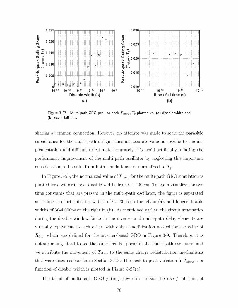
10-130.010
0.015
0.020
0.025
0.030
(b)
Rise / fall time (s)10-12 10-11 10-10
Pe
ak
-to
-pe
ak
Ga
tin
g S
ke
w
(Tskew
/ T
q)
10-130
0.005
0.010
0.015
0.020
0.025
(a)
Disable width (s)10-12 10-11 10-8
Pe
ak
-to
-pe
ak
Ga
tin
g S
ke
w
(Tskew
/ T
q)
10-10 10-9
Figure 3-27 Multi-path GRO peak-to-peak Tskew/Tq plotted vs. (a) disable width and(b) rise / fall time
sharing a common connection. However, no attempt was made to scale the parasitic
capacitance for the multi-path design, since an accurate value is specific to the im-
plementation and difficult to estimate accurately. To avoid artificially inflating the
performance improvement of the multi-path oscillator by neglecting this important
consideration, all results from both simulations are normalized to Tq.
In Figure 3-26, the normalized value of Tskew for the multi-path GRO simulation is
plotted for a wide range of disable widths from 0.1-4000ps. To again visualize the two
time constants that are present in the multi-path oscillator, the figure is separated
according to shorter disable widths of 0.1-30ps on the left in (a), and longer disable
widths of 30-4,000ps on the right in (b). As mentioned earlier, the circuit schematics
during the disable window for both the inverter and multi-path delay elements are
virtually equivalent to each other, with only a modification needed for the value of
Rinv, which was defined for the inverter-based GRO in Figure 3-9. Therefore, it is
not surprising at all to see the same trends appear in the multi-path oscillator, and
we attribute the movement of Tskew to the same charge redistribution mechanisms
that were discussed earlier in Section 3.1.3. The peak-to-peak variation in Tskew as a
function of disable width is plotted in Figure 3-27(a).
The trend of multi-path GRO gating skew error versus the rise / fall time of
78
Enable also appears very similar to the inverter-based GRO results discussed earlier,
with a slight decrease of variation in Tskew for slower Enable transitions. This result is
seen most clearly in the plot of peak-to-peak variation in Tskew as shown in Figure 3-
27(b). To recapilutate an earlier comment, a slower Enable may suffer from increased
thermal and 1/f noise contributions, although it does seem to provide some benefit
in terms of smoothing out the gating skew error.
By providing a physical intuition as well as simulation results, we can conclude that
the gating skew error for the proposed multi-path GRO architecture is significantly
reduced compared to the inverter-based topology. We can also say that there are two
key features of the proposed multi-path oscillator design that enable such a marked
improvement in the gating skew error. First, the large number of delay elements in
transition at any given time means that the overall gating skew has the potential to be
influenced by more than one delay element. Second, the distributed set of connections
in this design, chosen originally to ensure oscillation in the primary mode, provide a
web that strongly couples the delay elements together. Together, these features enable
a very digital circuit structure to accurately preserve the analog state information that
is required for noise-shaping. We will later see in Chapters 5 and 6 that this level of
gating skew performance is inherently sufficient to achieve robust first-order shaping
of the quantization and mismatch error.
79

80
Chapter 4
GRO readout techniques
4.1 Measurement entirely with counters
As shown earlier in Figure 2-11, a simple technique for keeping track of the GRO
phase transitions for a given measurement interval is to simply count the number of
transitions for each output, and then sum the counter values to result in the TDC
output. Figure 4-1 illustrates that for the most basic implementation, two counters
are in fact required for each output stage to account for both the positive and the
negative transitions. For a moderate number of stages (<20) in a standard ring
oscillator, in terms of power and area, the overall penalty of having two counters for
each stage is modest. We will see later that for the multi-path ring oscillator the
penalty in power is more severe.
Other than efficiency, there are more subtle concerns with this simple counting
technique when it comes to ensuring that each transition is counted the correct num-
ber of times. The counters in a GRO-TDC have two unique considerations in that
the“digital” inputs are asynchronous signals with voltages that can often be held at
undefined logic levels. Since achieving any noise-shaping at all relies on precisely ac-
counting of GRO phase error, miscalculation of the phase transitions is unacceptable
for the GRO-TDC.
To deal with the first issue of asynchronous counter inputs, an obvious solution
is to latch the delay element outputs before the counter needs to be sampled. The
81

N-Stage Gated Ring Oscillator
ResetStart
Stop
Logic
Register
Count[k]
e[k]
Counters
Enable
Figure 4-1 Using two counters for each output stage to keep track of the total numberof phase transitions
Counter
Output
to Adder
GRO Delay
Element OutputLatch Counter
CLKlatch
Enable
CLKlatch
Latch Input
Counter Input
Counter Output
GRO Output
12!
10
(a) (b)
Figure 4-2 Double-counting transitions in the GRO measurement due to ambiguity indelay element output logic levels. (a) Double-counting example, and (b) Suppressing theglitch with a carefully timed latch control signal
counter input simply needs to be latched early enough to guarantee that the ripple
counter has properly settled from the time of the last possible input transition.
The second issue of dealing with counter inputs that are stopped at invalid logic
levels can be helped somewhat by a few obvious circuits, however addressing the
82

fundamental issue is more complex. For example, buffering and using positive feed-
back for delay stage outputs very close to a logical threshold can virtually eliminate
metastability problems, but this does not decrease the possibility of the delay stage
output moving across the threshold during the disabled window. As shown in Fig-
ure 4-2(a) without additional measures in place, the counter can advance more than
one count for a single transition event.
One possible solution to address this double-counting of transitions is to de-glitch
the negative pulse with a carefully timed latch control signal. Figure 4-2(b) illustrates
that after the GRO is enabled, the delay element output in question will quickly
resolve itself to a logical state that it will hold for a relatively long time (≈ NTinv).
By opening the latch slightly after Enable ↑ (but well before the next transition),
any potential glitches at the counter input will be removed.
When contemplating how phase measurement entirely with only counters can be
used for the multi-path oscillator, there are two primary areas of concern. First, while
30 counters operating at a relatively slow rate (<1GHz) does not consume much area
or power for the standard inverter GRO [21], the situation worsens considerably for
the multi-path oscillator, which would require 94 counters operating at approximately
2GHz. Second, de-glitching the counter inputs by means of careful timing is not a
robust technique that can easily be implemented with simple digital synthesis tech-
niques. Although it is understood that the GRO core has custom attributes, we would
prefer a more elegant solution that is robust even when implemented by relatively
crude automation.
4.2 A more efficient measurement technique
In this section we describe an efficient and robust phase measurement technique that
is applicable to a wide range of ring oscillators. Compared to the previous approach,
which operates on each delay element outputs independently, the foundation for this
technique takes advantage of the predictable sequencing of oscillator transitions. In
this way, the motivation for both the multi-path oscillator topology and the phase
83

measurement approach is that the designer can anticipate known phase state patterns
to make decisions more intelligently. However, we will first continue to use the stan-
dard oscillator in this section to illustrate the concepts of this technique, and later
apply the concepts to the multi-path oscillator. We also present a robust de-glitch
circuit that does not require precision timing to avoid double-counting.
4.2.1 Measuring frequency by tracking phase
For the GRO, counting the delay element outputs is, by far, more expensive in terms
of area and power than is sampling the output with a digital register, since in general
the TDC sampling rate is much slower than the oscillation frequency. Yet, a single
counter provides a full record of its input transitions since its last reset, whereas an
undersampled single register appears to provide no transition information at all. In
fact, a single register only provides a crude sample of the phase of the oscillator.
However, we know that the GRO frequency and phase are related by
fGRO[k] =∆θ[k]
Ts
, (4.1)
and we can then say that
1
2NTq
=θGRO[k] − θGRO[k − 1]
2πTin[k](4.2)
πTin[k]
NTq= θGRO[k] − θGRO[k − 1] (4.3)
π
N
(
Out[k] +Terror[k]
Tq
)
= θGRO[k] − θGRO[k − 1] (4.4)
Out[k] =N
π
(
θGRO[k] − θGRO[k − 1])
−Terror[k]
Tq. (4.5)
We see that it is not only possible to estimate frequency indirectly via phase, but the
noise-shaping properties of the GRO-TDC are also preserved through Terror. There-
fore, calculating phase by using N registers appears very attractive compared to
tracking frequency with 2N counters.
Figure 4-3 illustrates the basic concept of calculating the GRO-TDC output by
84

15-Stage Gated Ring Oscillator
Start
Stop
Logic State-to-Phase Logic
Registers
Enable
CountResidue
Out[k]
Differentiator
Phase[k]
Counter
x2N Multiplier
Enable
QuantizedPhase
Residual(max = 30)
Tin[k]
Out[k]
26
20
33
Out[k-1]
Out[k]
56
3
6030Phase
Count30
Phase[k]
-Phase[k-1] -50
6
63
-56
7
Figure 4-3 Basic concept of calculating the GRO-TDC output by differentiating phase
quantizing the oscillator phase with registers, and then differentiating from sample to
sample. Of course, the problem with using only registers to measure the average GRO
frequency (or number of transitions) is that the oscillator phase value is calculated
modulo 2N (or 2π, depending on units), and without a means to keep track of the
number of phase wraps, the measurement output will be incorrect. To solve this
problem, we separate the phase into two components, a fine phase residual that is
calculated from the registers, and a coarse phase that accumulates 2N (in the figure
N = 15) each time the oscillator phase wraps around without a reset operation.
The coarse phase accumulation can simply be implemented by counting the positive
transitions of a chosen delay element.
To accurately calculate the phase residual we need to observe the entire oscillator
state, which means utilizing the outputs from all the delay elements. The key idea here
is to leverage a simple, predictable mapping between the sampled oscillator output
code and phase that is inherent in the fundamental operation of the oscillator. For
example, Figure 4-4 charts how the 30 possible phase states of the example 15-stage
ring oscillator are encoded in the delay element output values. The starting phase,
or equivalently the state mapping to zero residual, is determined by the polarity and
location of the counted delay element. To calculate a binary-coded phase residue for
85
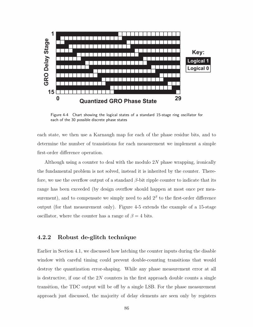
1
15
GR
O D
ela
y S
tag
e
Quantized GRO Phase State0 29
Logical 1
Logical 0
Key:
Figure 4-4 Chart showing the logical states of a standard 15-stage ring oscillator foreach of the 30 possible discrete phase states
each state, we then use a Karnaugh map for each of the phase residue bits, and to
determine the number of transistions for each measurement we implement a simple
first-order difference operation.
Although using a counter to deal with the modulo 2N phase wrapping, ironically
the fundamental problem is not solved, instead it is inherited by the counter. There-
fore, we use the overflow output of a standard β-bit ripple counter to indicate that its
range has been exceeded (by design overflow should happen at most once per mea-
surement), and to compensate we simply need to add 2β to the first-order difference
output (for that measurement only). Figure 4-5 extends the example of a 15-stage
oscillator, where the counter has a range of β = 4 bits.
4.2.2 Robust de-glitch technique
Earlier in Section 4.1, we discussed how latching the counter inputs during the disable
window with careful timing could prevent double-counting transitions that would
destroy the quantization error-shaping. While any phase measurement error at all
is destructive, if one of the 2N counters in the first approach double counts a single
transition, the TDC output will be off by a single LSB. For the phase measurement
approach just discussed, the majority of delay elements are seen only by registers
86

Enable
QuantizedPhase
Residual
Tin[k]
360
30
480
0
Phase Count(max = 24.30)
450
Overflow
510
4
2415
Out[k]
-384-Phase[k-1]
Overflow[k] 0
70
-454
480
71
454Phase[k] 45
Figure 4-5 Accomodating a counter with a limited range of 2β levels (here β = 4)
which are much less sensitive to glitch events. However, if a double-counting error in
the counter is made in this topology, it is likely that the TDC output will be wrong
by at least 2N , since the counter output is amplified by this value. This magnitude of
error lacks noise-shaping and would likely be very disruptive at the application level.
The first step that we take to remove counting glitches is again to latch the counter
input, as seen in Figure 4-6. The delay element output to be counted, Vocount, is then
input to both a latch as well as a register, since its state information is required for
both the phase count as well as the phase residue. Putting aside the issue of double-
counting for now, we can see another potential source of phase measurement error
that the latch output is not guaranteed to be the same as the register output. The two
distinct samplers will undoubtedly have different offset and sampling instants, which
is problematic since the GRO output Vocountcan be held near mid-supply during the
disable times. Although in noise-shaping applications it is likely that a latch/register
87

Enable
CLK
GROOutput Vocount
LatchOutput Lcount
RegisterOutput Rcount
The latch
and register
may resolve
the same input
different ways!
N-Stage Gated Ring Oscillator
Start
Stop
Logic
State-to-Phase Logic
Registers
Enable
CountResidue
Out[k]
Differentiator
Phase[k]
Counter
x2N Multiplier
LatchCLK
Vocount
Rcount
Lcount
Figure 4-6 A potential phase error when the oscillator state is determined by both reg-isters and counters
(c)
CounterCLK
Vocount
Lcount
Latch
Rcount
Latch
(a)
Counter
Latch
CLK
Vocount
Lcount
Register
Rcount
(b)
Counter
Latch
CLK
Vocount
Lcount
Latch
Rcount
Latch
Figure 4-7 Combining register and latch functions into a single element to resolve thepotential discrepancy between register and latch outputs. (a) shows the original problem-atic implementation, (b) illustrates that a D flip-flop is composed of two serial D latches,and (c) combines the redundant latches to ensure the same signal is observed by boththe register and the counter.
discrepancy would be corrected in the next sample, the TDC outputs for at least two
samples would be incorrect, which is generally unacceptable.
A very efficient way to resolve the potential discrepancy between the latch and
register outputs is to utilize a common latch circuit for both functions. Figure 4-7
illustrates that we can implement a D flip-flop register as a master-slave pair of D
latches, and coincidentally in (b) we find that the first D function is implemented by
both the register as well as the latch. As seen in (c), we can eliminate a redundant
latch, and at the same time achieve a unified signal path that will ensure the phase
count and phase residual are consistent with each other (note that in this statement
88

we rely on a monotonically increasing phase during the enabled window).
With assurance of a consistent phase count and phase residue, we now focus on
the issue of double-counting errors due to glitches at the counter inputs (as discussed
earlier in regard to Figure 4-2). Instead of clocking the latch signals with precisely
controlled timing, we can avoid glitches with a more robust technique that once again
leverages the predictable sequence of the oscillator phase state.
Recall that the goal for the de-glitch circuit is to ensure that the counter incre-
ments exactly once for each GRO phase rotation, regardless of how slowly the counter
voltage threshold is crossed, or even how many times the threshold is crossed! There-
fore, the key idea for the proposed de-glitch circuit is the knowledge that when the
counter input Vocountis held near mid-supply, almost all the other stages are resolved
to unambiguous logic levels.
Specifically, if Vocountis transitioning high at the time Enable ↓, then we can say
with certainty that a delay element output Vode−glitchpreceding Vocount
by a small, even
number of stages (e.g. Vode−glitch= Zcount−2) has just competed its positive transition.
Similarly, the negative transitions follow in the same sequence. Therefore, we can say
that to prevent the counter input from “moving backward”, it should only transition
when both Vode−glitchand Vocount
share the same logic level. A truth table for the de-
glitch logic can seen in Table 4.1, where Lde−glitch and Lcount are defined as the latch
outputs corresponding to Vode−glitchand Vocount
, respectively, and Lcd is the de-glitch
logic output.
Lde−glitch Lcount Lcd
1 1 11 0 No change0 1 No change0 0 0
Table 4.1 Truth table for the de-glitch logic
Figure 4-8 shows one circuit realization of the de-glitch logic using a four-transistor
stack along with weak regeneration. When both Vode−glitchand Vocount
share the same
logic level, the appropriate pull-up or the pull-down network is active. Alternately, if
89
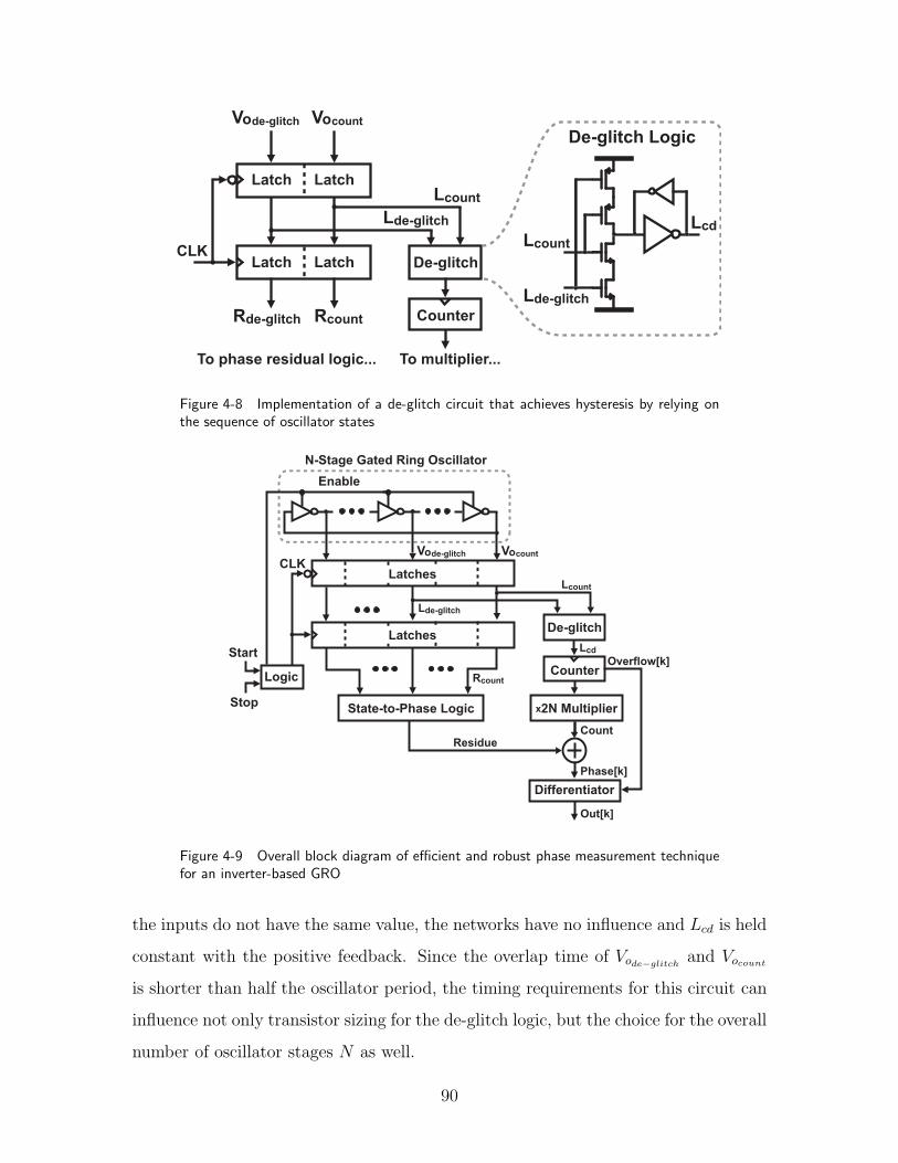
To multiplier...To phase residual logic...
De-glitchCLK
Vocount
Lcount
Latch
Rcount
Latch
Counter
Latch
Latch
Vode-glitch
Rde-glitch
Lde-glitch
De-glitch Logic
Lcount
Lde-glitch
Lcd
Figure 4-8 Implementation of a de-glitch circuit that achieves hysteresis by relying onthe sequence of oscillator states
N-Stage Gated Ring Oscillator
Start
Stop
Logic
State-to-Phase Logic
Latches
Enable
CountResidue
Out[k]
Differentiator
Phase[k]
Counter
x2N Multiplier
CLKVocount
Lcd
Vode-glitch
De-glitchLatches
Overflow[k]
Rcount
Lcount
Lde-glitch
Figure 4-9 Overall block diagram of efficient and robust phase measurement techniquefor an inverter-based GRO
the inputs do not have the same value, the networks have no influence and Lcd is held
constant with the positive feedback. Since the overlap time of Vode−glitchand Vocount
is shorter than half the oscillator period, the timing requirements for this circuit can
influence not only transistor sizing for the de-glitch logic, but the choice for the overall
number of oscillator stages N as well.
90
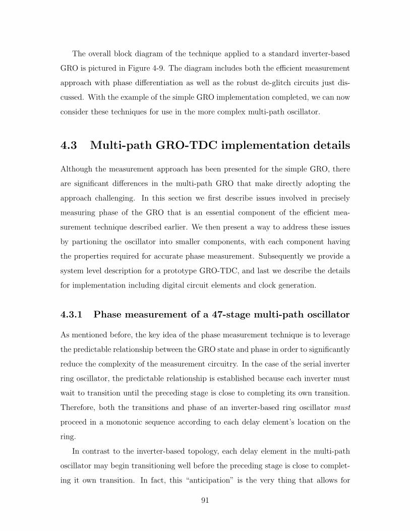
The overall block diagram of the technique applied to a standard inverter-based
GRO is pictured in Figure 4-9. The diagram includes both the efficient measurement
approach with phase differentiation as well as the robust de-glitch circuits just dis-
cussed. With the example of the simple GRO implementation completed, we can now
consider these techniques for use in the more complex multi-path oscillator.
4.3 Multi-path GRO-TDC implementation details
Although the measurement approach has been presented for the simple GRO, there
are significant differences in the multi-path GRO that make directly adopting the
approach challenging. In this section we first describe issues involved in precisely
measuring phase of the GRO that is an essential component of the efficient mea-
surement technique described earlier. We then present a way to address these issues
by partioning the oscillator into smaller components, with each component having
the properties required for accurate phase measurement. Subsequently we provide a
system level description for a prototype GRO-TDC, and last we describe the details
for implementation including digital circuit elements and clock generation.
4.3.1 Phase measurement of a 47-stage multi-path oscillator
As mentioned before, the key idea of the phase measurement technique is to leverage
the predictable relationship between the GRO state and phase in order to significantly
reduce the complexity of the measurement circuitry. In the case of the serial inverter
ring oscillator, the predictable relationship is established because each inverter must
wait to transition until the preceding stage is close to completing its own transition.
Therefore, both the transitions and phase of an inverter-based ring oscillator must
proceed in a monotonic sequence according to each delay element’s location on the
ring.
In contrast to the inverter-based topology, each delay element in the multi-path
oscillator may begin transitioning well before the preceding stage is close to complet-
ing it own transition. In fact, this “anticipation” is the very thing that allows for
91

Time
Vo
lta
ge
Figure 4-10 Simulated transient voltages of the multi-path delay element outputs whenmismatch is included
significant reduction of the effective delay per stage. As a result, we have already
seen in Figure 3-23 how approximately 13 delay elements in the proposed multi-path
oscillator are in transition at any instant.
When considering a practical implementation, Figure 4-10 shows an example of
delay element output transient voltages when the simulation includes the effect of
mismatch. For this plot, mismatch was assumed for the transistors as well as for a
small parasitic capacitance with 20% standard deviation. In this figure, note that a
few of the transitions moving in the same direction appear to be very close together,
and at other times the transitions are more spread apart. The differential non-linearity
is not a problem in and of itself for the GRO-TDC, since this error is first-order
shaped. However, the close proximity of edges does pose a problem for the efficient
phase measurement techniques that we would like to use.
Recall that the quantized GRO state is encoded with the logical value of the delay
element outputs, and that mapping from the GRO state to phase requires knowing the
exact transition sequence that delay elements will undergo during oscillation. In this
case, the sequence of transitions may be deterministic within a specific realization, but
this sequence is almost impossible to predict, and in addition there is the possibility
92
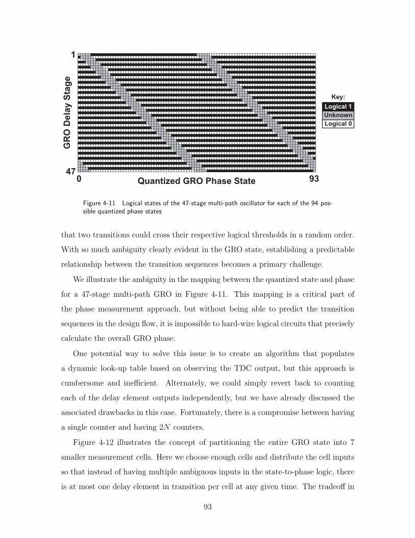
1
47
GR
O D
ela
y S
tag
e
Quantized GRO Phase State0 93
Logical 1
Logical 0
Unknown
Key:
Figure 4-11 Logical states of the 47-stage multi-path oscillator for each of the 94 pos-sible quantized phase states
that two transitions could cross their respective logical thresholds in a random order.
With so much ambiguity clearly evident in the GRO state, establishing a predictable
relationship between the transition sequences becomes a primary challenge.
We illustrate the ambiguity in the mapping between the quantized state and phase
for a 47-stage multi-path GRO in Figure 4-11. This mapping is a critical part of
the phase measurement approach, but without being able to predict the transition
sequences in the design flow, it is impossible to hard-wire logical circuits that precisely
calculate the overall GRO phase.
One potential way to solve this issue is to create an algorithm that populates
a dynamic look-up table based on observing the TDC output, but this approach is
cumbersome and inefficient. Alternately, we could simply revert back to counting
each of the delay element outputs independently, but we have already discussed the
associated drawbacks in this case. Fortunately, there is a compromise between having
a single counter and having 2N counters.
Figure 4-12 illustrates the concept of partitioning the entire GRO state into 7
smaller measurement cells. Here we choose enough cells and distribute the cell inputs
so that instead of having multiple ambiguous inputs in the state-to-phase logic, there
is at most one delay element in transition per cell at any given time. The tradeoff in
93

Unpredictabletransitionsequence
Enable/Enable
(b)
Onetransitionper cell
1234567
Enable/Enable
(a)
Figure 4-12 A geometric view of an example multi-path GRO state illustrating (a) theunpredictable transition sequence considering the entire multi-path oscillator, and (b) apartitioned approach that re-establishes predictable transition sequences within each ofthe 7 independent measurement cells
this approach is the increased power of having one counter for each cell instead of one
counter for the entire GRO. This small penalty is far outweighed by re-establishing
the predictable sequence of states, at least with respect to each individual cell. The
measurement cells can then independently calculate their outputs, which are then
simply summed together in the final step to result in the overall TDC output.
The interesting aspect to this approach is that although we have separated the
entire GRO state into independent groups for purposes of measurement, we have not
altered any of the GRO properties. In fact, as shown in Figure 4-13(a), by simply
rearranging the outputs in a convenient manner, the ambiguity in the overall GRO
phase state has not actually been resolved. Instead, as shown in (b), the phase state
for each cell is now predictable and internally self-consistent. From this perspective,
these 7 cells may be seen as coupled oscillators, although in this case we do not require
all of the cells to be equivalent, nor do we require a conventional pattern for the state
sequence.
For convenience it is simpler to have one measurement cell repeated multiple times,
however the prime number of GRO stages is more important for stability reasons. In
94

Cell 7
GR
O D
ela
y S
tag
es
Quantized GRO Phase State0 93
Logical 1
Logical 0
Unknown
Key:
Cell 6
Cell 5
Cell 4
Cell 3
Cell 2
Cell 1
Quantized Cell Phase State
Logical 1
Logical 0
Key:
0 9
Cell with
5 inputs
Cell with
7 inputs
0 13
Delay
Stage
Outputs
(a)
(b)
Figure 4-13 Re-arranging the logical states of the multi-path GRO into groups thatcorrespond to the 7 measurement cells. (a) charts the ambiguity in the overall GROphase state, and (b) charts the predictable phase state for the smaller cells
general, it is possible to have only two kinds of cells, and here we choose to have 6
cells with 7 inputs each, and 1 cell with 5 inputs. The assignment of delay elements
to cells is shown in Table 4.2, and we note that the first pair of inputs for each cell
are separated by 6 stages to use in the de-glitch logic.
Finally, we now show a system block diagram for the proposed 47-stage multi-path
GRO-TDC in Figure 4-14. Although we have discussed at some length the GRO core
and the measurement cells, a few other digital circuit blocks are also needed within
the TDC. The timing generation block takes a start and stop signal input, generates
the differential Enable signal, and sufficienctly buffers Enable in order to drive the
95

1.1 11.2 71.3 141.4 211.5 281.6 351.7 42
2.1 22.2 82.3 152.4 222.5 292.6 362.7 43
3.1 33.2 93.3 163.4 233.5 303.6 373.7 44
4.1 44.2 104.3 174.4 244.5 314.6 384.7 45
5.1 55.2 115.3 185.4 255.5 325.6 395.7 46
6.1 66.2 126.3 196.4 266.5 336.6 406.7 47
7.1 137.2 207.3 277.4 347.5 41
Table 4.2 Assignment of delay element outputs to measurement cell inputs
Timing Generation
Out
Enable 47-stageGated Ring Oscillator
StateRegister
Start
Stop
Adder
Z1-47
MeasurementCells
Start
Stop
Enable
CLK
CLK
1 72 3 4 5 6
Figure 4-14 Overall system block diagram for the proposed 47-stage multi-path GRO-TDC
GRO core with modest rise and fall times (and correspondingly modest jitter). In
addition, the timing generation block derives the other clocking signals as required by
the measurement cells. Last, the output adder receives all of the calculated outputs
from each of the measurement cells and sums them to result in the overall GRO-TDC
output.
4.3.2 Other design considerations
Although the GRO-TDC can easily accommodate very large range input signals by
adding bits to the counters, the penalty for doing so is an increase in the minimum
length of the disable time, since these counters must fully settle and be sampled
before the oscillator can be enabled again. In addition, the processing time for a
96
large number of bits can increase the pipeline delay of the measurement cells and
output adder significantly if very high-speed operation also must be supported. Low
pipeline delay is important in many closed-loop applications because it can pose an
upper limit on the loop bandwidth. Therefore, design of the overall TDC must trade
the parameters of maximum sampling rate, maximum range, and acceptable pipelined
delay against each other to find an appropriate balance.
For our prototype demonstrations, we chose to implement two versions of the
GRO-TDC, with specifications determined by the system applications. The multi-
path GRO core is common and, assuming a minimum resolution design takes first
priority, can be used for a very wide range of applications. The first TDC is a general
purpose 11-bit, 100Msps version that can typically be used for systems comparing to
crystal references such as PLL and multiplying DLL [21, 25]. The second version is
an 8-bit, 500Msps TDC that can be used in high-speed timing applications such as
CDR. These various applications will briefly be discussed later in Chapter 6.
97

98

Chapter 5
GRO-TDC results and discussion
At this point, the concept of a gated ring oscillator TDC has been introduced, and
a number of design considerations have been discussed that relate to overall per-
formance, for example raw resolution, gating skew error, measurement precision,
efficiency, and range vs. sampling rate. To demonstrate how these considerations
relate to a practical implementation, a total of three GRO-TDC were designed and
fabricated in 0.13µm CMOS technology.
The first GRO-TDC is based on a simple 15-stage inverter-based oscillator core,
and has a 10-bit measurement range using only counters. The second and third GRO-
TDC are based on the same multi-path GRO that is described in 3.2.2, and both use
the efficient readout techniques described in Section 4.3. The difference between these
two GRO-TDC, then, is the range and maximum operating frequency, with a 8-bit,
500Msps part and an 11-bit, 100Msps version. A single microphotograph depicting an
11-bit GRO-TDC 1.0mm×1.0mm die is shown in Figure 5-1, which is nearly identical
to the other die in terms of visible markings.
In this chapter, we first describe the requirements and proposed approach for the
measurement setup. Next, we present measurement results for the inverter-based
GRO-TDC, including the non-linear effects of the gating skew error for this imple-
mentation such as corrupted noise shaping and deadzones. Then, measurements of
the 11-bit multi-path GRO-TDC are shown, which verifies the inherent noise-shaping
capability of the GRO-TDC architecture. Finally, we conclude this section with a
99

1.0 mm
1.0
mm
GRO-TDC
157x258µm
Figure 5-1 Microphotograph of a multi-path GRO-TDC chip
discussion of the results.
5.1 Measurement setup
The GRO-TDC can measure a time difference between edges created by two distinct
time sources, however the overall jitter in such a measurement is significantly larger
than the internal TDC noise. Instead, a preferred way to take data is to measure
the delay of a single time source, as shown in Figure 5-2, which removes the noise
contributions from the source entirely. Although there is some noise contribution
from the delay element itself, this is expected to be comparable to the internal TDC
noise itself.
There are two primary issues with using the modulated delay method to create
an input signal to the TDC. The first problem is that it is very difficult to create
a large signal that spans the entire TDC range, and the second problem is that
the linearity performance for large signals is generally quite poor. Although pulse-
width modulation can be used to achieve very high linearity for audio frequencies,
achieving such linearity with low noise at 50Msps with discrete parts is actually
quite challenging. Therefore, we have chosen to implement the variable delay by
100

GRO-TDC
EnableS QR
VariableDelay GRO
Logic Out[k]
Figure 5-2 A method to create a low-noise input signal for the GRO-TDC testing
modulating the power supply of an off-chip buffer, which is suitable for measuring
the GRO-TDC noise performance with relatively small input signals. This signal
generation capability is designed onto a gold-plated FR-4 circuit board, which also
provides power supplies, decoupling capacitors, and a substrate for direct-bonding of
the GRO-TDC chips.
Due to the limitations just discussed for generating large input signals, we choose
to use two synchronized signal generators to verify large-signal performance across
the full range of the GRO-TDC. In this setup, the frequency and phase of the first
signal is held constant, and the second signal generator can be phase modulated to
create a time difference that fully spans the GRO-TDC range. Again, the quality
of the input in terms of both noise and linearity using this approach is quite poor,
however the measurement does establish a full-scale signal level for the TDC.
5.2 Inverter-based GRO-TDC measurements
Current consumption of the inverter-based GRO-TDC from a 1.2V supply is a linear
function of the duty cycle of the input, and ranges from 1.7mA with 2% activity to
4.4mA at 80% (2.0 to 5.3mW). Of the 1.0mm×1.0mm chip with 20 pads, this GRO-
TDC requires only 172µm×120µm of active area, not including decoupling capacitors,
and the GRO core is 66µm×19µm. The input range of the 10-bit TDC is 0.2-45ns,
101

104 105 106 107
Frequency (Hz)
-100
-80
-60
-40
-20
0
20P
ow
er
Sp
ectr
al D
en
sit
y
(dB
ps
2/H
z)
65,536 pt. FFTHanning window
25
50
55
60Raw TDC Output
Filte
red
TD
C O
utp
ut
Time (µs)
0 5 10 15
(a)(a) (b)
35
40
45
30
Figure 5-3 Measured 65,536-pt. FFT of an inverter-based GRO-TDC output
and the minimum sampling period is 4nsec as required for timing control. For all
reported measurements, the nominal sampling rate is 50MHz.
To properly scramble the GRO phase and achieve reasonable noise-shaping, a
relatively large, asynchronous input to the TDC is required. An example of this case is
shown in Figure 5-3(a) with an input that is phase-modulated at a rate of 150kHz and
at a amplitude of 0.25rad. The 65,536-point FFT spectrum with Hanning windowing
does in fact show some level of noise-shaping at high frequencies near 25MHz, or Fs/2,
and the time-domain view appears perfectly normal in Figure 5-3(b). However, we
can notice the very high noise floor that is caused by scrambling the large gating skew
error. With the noise levels in the figure normalized to show an equivalent two-sided
power spectral density, the high noise floor corresponds with the ideal variance from
a classical quantizer with 25-30ps resolution sampling at the same rate of 50MHz.
This level of noise is much larger than 1/f or thermal noise limitations, and implies
that the noise-shaping benefit is small for the inverter-based GRO-TDC.
While the measurement shown in Figure 5-3 does not achieve a low noise floor,
it does represent a fairly linear behavior compared to other measurement scenarios.
There are many other inputs that can be applied to the inverter-based GRO-TDC
that do not result in adequate scrambling of the GRO phase, and the resulting non-
102

105 106 107
Frequency (Hz)
-120
-100
-80
-60
-40
-20
Po
we
r S
pe
ctr
al
De
ns
ity
(dB
ps
2/H
z)
65,536 pt. FFTHanning window
No physical noise floor!
Figure 5-4 An example of non-linear behavior in the inverter-based GRO-TDC
Variable Delay Control Input15
16
17
18
19
20
Avera
ged
GR
O-T
DC
Ou
tpu
t
13.55
13.70
13.80
13.90
Avera
ged
GR
O-T
DC
Ou
tpu
t
(a)(a) (b)
13.65
13.75
13.85
13.60
Variable Delay Control Input
11ps
Figure 5-5 A measured DC transfer characteristic for the inverter-based GRO-TDC thatdemonstrates the presence of deadzones. (a) indicates the deadzone behavior for integerTDC outputs, and (b) shows the potential for small deadzones at non-integer outputvalues.
linearity can be clearly seen in the TDC output. For example, in Figure 5-4, an
input that is synchronously modulated at 12.5MHz is applied to the GRO-TDC, and
the FFT spectrum clearly first-order noise-shaping. However, the figure also reveals
non-linear behavior since there is no observable noise floor in the TDC output.
The issue of deadzones in the DC transfer characteristic as a result of gating skew
non-linearity was theoretically discussed earlier in Section 3.1.4, and this behavior
103

can also been seen experimentally in the inverter-based GRO-TDC. To generate a DC
signal for the GRO-TDC, the variable testing delay is controlled with a digital-to-
analog converter, and in this particular measurement setup the overall tuning system
is quite non-linear. Nevertheless, a DC transfer characteristic of the inverter-based
GRO-TDC is plotted in Figure 5-5. The deadzone behavior at the integer boundaries
is clearly evident in (a), with larger deadzone widths for the even TDC outputs as
predicted from simulations. Closer examination of the curve in (b) reveals that much
smaller deadzones are possible for some non-integer TDC outputs as well.
5.3 Multi-path GRO-TDC measurements
Within the 1.0mm×1.0mm chip, the active silicon area of the larger 11-bit GRO-
TDC is 258µm×157µm, and the area of the 8-bit chip is 217µm×143µm, which both
include a guardring but exclude power supply decoupling capacitors. The area for
the shared 47-stage multi-path GRO core is 88µm×54µm. All measurements reported
here are using the 11-bit part at 50Msps, since at this sampling rate and with output
values less than 8-bits, the parts are verified to have identical functionality.
5.3.1 Delay, power, and efficiency performance
A 1.5V supply is used in general for measurements, and functional operation was
verified from 1.0-1.6V. As shown in Figure 5-6, the raw delay per stage of the GRO is
a strong function of the power supply, and has a nominal value of 6ps at 1.5V. Also
as expected, the power consumption of the GRO-TDC is measured to be a linear
function of the width of the input signal. At 50Msps, the minimum power is 2.2mW
for a very small input, and the maximum is 21mW for full-scale.
The measured multi-path delay of 6ps represents an improvement factor of over
5 compared to an inverter-based GRO-TDC delay of 30-35ps under the same voltage
supply and operating conditions. This result verifies the significant benefit in raw
resolution that multi-path oscillators can offer for TDC applications. Recall that in
Section 3.2.1, we defined Jeff to be the product of a weighted sum of multi-path
104

1.0 1.1 1.2 1.3 1.4 1.54
8
10
12
GR
O D
ela
y / S
tag
e (
ps)
Power Supply Voltage (V)
6
Figure 5-6 Measured delay per stage for the multi-path GRO vs. power supply voltage
connections with an efficiency factor, η. Now with the measured results in place, we
can calculate Jeff of the multi-path design to be 5, and using the values of J and W
given in Table 3.1, we find that
Jeff = ηK∑
k=1
wk · jk, (5.1)
5 = η (13 · 0.25 + 11 · 0.16 + 9 · 0.24 + 5 · 0.24 + 1 · 0.12) , (5.2)
η = 0.60. (5.3)
Therefore, while this particular design has lost a small amount of efficiency due to
implementation parasitics compared to the improvement that might be expected from
unextracted simulations, the speed benefit compared to the inverter-based implemen-
tation is still very significant.
A typical method to measure efficiency for converters is by the standard figure of
merit, P/Fs/2ENOB. Although it is difficult to calculate the effective number of bits
for the TDC in a manner comparable to a classical ADC, as an alternative we can
use an efficiency figure of merit defined by
FOM =Power
(Sampling Rate)(Conversion levels)(5.4)
105

=21 × 10−3
(50 × 106)(211)(5.5)
= 0.2pJ/step. (5.6)
The GRO-TDC compares favorably with other TDC in this metric, yet there is a
fundamental flaw in this FOM because it does not appropriately factor the TDC res-
olution. For example, a very large range can easily be achieved by using a cyclic TDC,
but this does not imply anything about the minimum detectable signal. Therefore,
we now move on to demonstrate the strength of the GRO-TDC, which of course is
the ability to achieve first-order noise-shaping.
5.3.2 Noise shaping performance
While the improved raw resolution is an important benefit of the multi-path oscillator,
recall that a fundamental design goal is to linearize the noise-shaping performance by
significantly reducing the gating skew. To examine whether this is accomplished with
the prototype GRO-TDC, we can apply very small input signals using the modulation
techniques described in the previous section. After collecting data in this way we can
examine the TDC output in both the time and frequency domain, and also in the DC
transfer characteristic to look for the presence of any non-linear deadzone behavior.
Figure 5-7 shows the both the frequency and time domain GRO-TDC 50-Msps
output with a 26kHz input of 1.2pspp in addition to a DC level of about 1.6ns. In
(a), the 65,536 point FFT is performed with a Hanning window on 20 sequential
collects before being averaged to result in the double-sided power spectral density as
shown. Noise-shaping of more than 20dB is clearly evident, with 1/f noise appearing
to dominate at low frequencies. The wide, shaded horizontal line in Figure 5-7 shows
that the low frequency power spectral density of the GRO-TDC output is comparable
to what ideally would be produced by a 50Msps classical quantizer (i.e. no noise
shaping) with 1ps steps.
By looking at the time domain output after digitally filtering with a 1MHz band-
width in Figure 5-7(b), the GRO-TDC is clearly able to resolve a 1.2pspp signal,
106
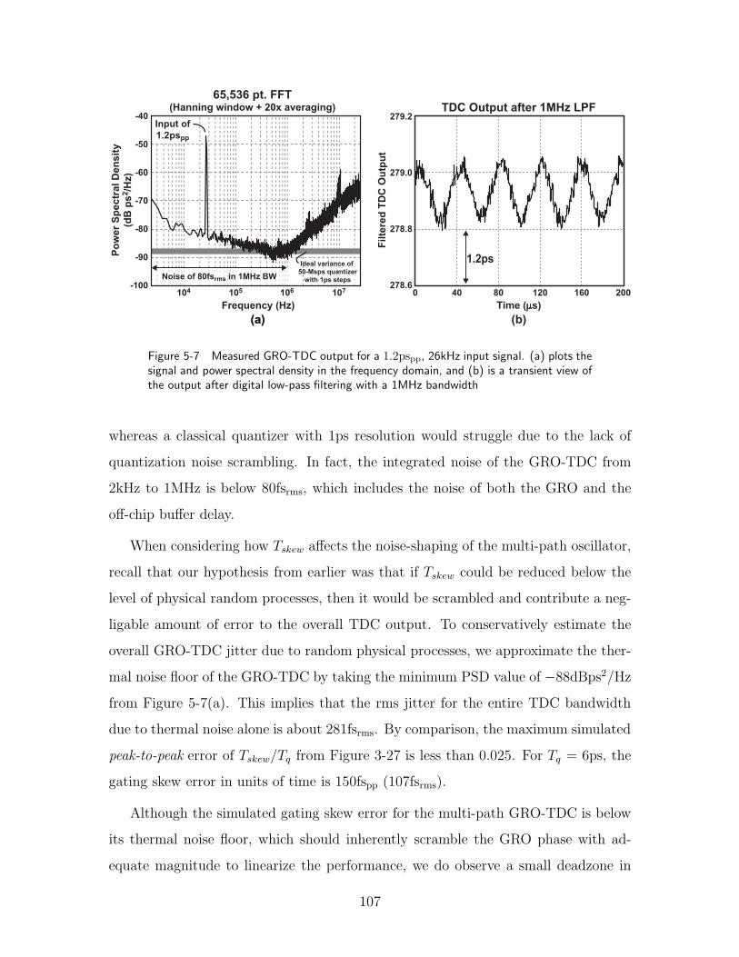
104 105 106 107
Frequency (Hz)
-100
-90
-80
-70
-60
-50
-40P
ow
er
Sp
ectr
al D
en
sit
y
(dB
ps
2/H
z)
65,536 pt. FFT(Hanning window + 20x averaging)
278.6
278.8
279.0
279.2TDC Output after 1MHz LPF
Filte
red
TD
C O
utp
ut
Time (µs)
0 40 80 120 160 200
Noise of 80fsrms in 1MHz BW
Input of
1.2pspp
Ideal variance of
50-Msps quantizer
with 1ps steps
1.2ps
(a)(a) (b)
Figure 5-7 Measured GRO-TDC output for a 1.2pspp, 26kHz input signal. (a) plots thesignal and power spectral density in the frequency domain, and (b) is a transient view ofthe output after digital low-pass filtering with a 1MHz bandwidth
whereas a classical quantizer with 1ps resolution would struggle due to the lack of
quantization noise scrambling. In fact, the integrated noise of the GRO-TDC from
2kHz to 1MHz is below 80fsrms, which includes the noise of both the GRO and the
off-chip buffer delay.
When considering how Tskew affects the noise-shaping of the multi-path oscillator,
recall that our hypothesis from earlier was that if Tskew could be reduced below the
level of physical random processes, then it would be scrambled and contribute a neg-
ligable amount of error to the overall TDC output. To conservatively estimate the
overall GRO-TDC jitter due to random physical processes, we approximate the ther-
mal noise floor of the GRO-TDC by taking the minimum PSD value of −88dBps2/Hz
from Figure 5-7(a). This implies that the rms jitter for the entire TDC bandwidth
due to thermal noise alone is about 281fsrms. By comparison, the maximum simulated
peak-to-peak error of Tskew/Tq from Figure 3-27 is less than 0.025. For Tq = 6ps, the
gating skew error in units of time is 150fspp (107fsrms).
Although the simulated gating skew error for the multi-path GRO-TDC is below
its thermal noise floor, which should inherently scramble the GRO phase with ad-
equate magnitude to linearize the performance, we do observe a small deadzone in
107
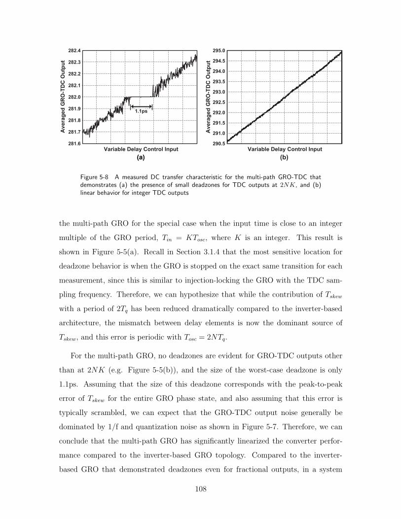
Variable Delay Control Input281.6
281.8
282.0
282.2
282.4
Av
era
ge
d G
RO
-TD
C O
utp
ut
(a)(a) (b)
Variable Delay Control Input
281.7
281.9
282.1
282.3
291.0
293.0
Av
era
ge
d G
RO
-TD
C O
utp
ut
292.0
294.0
295.0
1.1ps
290.5
292.5
291.5
293.5
294.5
Figure 5-8 A measured DC transfer characteristic for the multi-path GRO-TDC thatdemonstrates (a) the presence of small deadzones for TDC outputs at 2NK, and (b)linear behavior for integer TDC outputs
the multi-path GRO for the special case when the input time is close to an integer
multiple of the GRO period, Tin = KTosc, where K is an integer. This result is
shown in Figure 5-5(a). Recall in Section 3.1.4 that the most sensitive location for
deadzone behavior is when the GRO is stopped on the exact same transition for each
measurement, since this is similar to injection-locking the GRO with the TDC sam-
pling frequency. Therefore, we can hypothesize that while the contribution of Tskew
with a period of 2Tq has been reduced dramatically compared to the inverter-based
architecture, the mismatch between delay elements is now the dominant source of
Tskew, and this error is periodic with Tosc = 2NTq.
For the multi-path GRO, no deadzones are evident for GRO-TDC outputs other
than at 2NK (e.g. Figure 5-5(b)), and the size of the worst-case deadzone is only
1.1ps. Assuming that the size of this deadzone corresponds with the peak-to-peak
error of Tskew for the entire GRO phase state, and also assuming that this error is
typically scrambled, we can expect that the GRO-TDC output noise generally be
dominated by 1/f and quantization noise as shown in Figure 5-7. Therefore, we can
conclude that the multi-path GRO has significantly linearized the converter perfor-
mance compared to the inverter-based GRO topology. Compared to the inverter-
based GRO that demonstrated deadzones even for fractional outputs, in a system
108

Raw
TD
C O
utp
ut
Time (µs)
0
500
1000
1500
2000
0 20 40 60 80 100
Figure 5-9 Raw measured GRO-TDC output for a 26kHz input signal with an amplitudenear full-scale
application avoiding the small range of GRO-TDC outputs that correspond with
2KN is relatively straightforward.
To illustrate the full 11-bit operation of the GRO-TDC, Figure 5-9 plots raw
output data from the chip when a 26kHz input is applied with amplitude near full-
scale. A frequency domain plot is not given in this case due to input signal quality
as described in the previous section. Nonetheless, with a full-scale of 11-bits, the
dynamic range in a 1MHz bandwidth is calculated to be 95dB, or an equivalent
range of 15.5-bits. The TDC efficiency from before earlier can now be calculated in
the 1MHz bandwidth to be 0.23pJ/step, which is almost identical to the efficiency
calculated with full bandwidth due to the GRO quantization noise-shaping.
A summary of the 11-bit GRO-TDC performance is shown in Table 5.1. Further
demonstration of the measured TDC performance can be seen in Chapter 6, where
the GRO-TDC has been proven in a number of system applications.
5.4 Discussion
Table 5.2 compares the prototype GRO-TDC to other reported CMOS TDC. Al-
though we notice that there are different examples of TDC with comparable perfor-
109
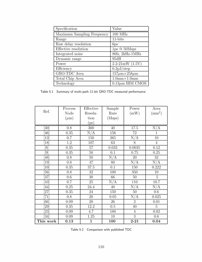
Specification Value
Maximum Sampling Frequency 100 MHzRange 11-bitsRaw delay resolution 6psEffective resolution 1ps @ 50MspsIntegrated noise 80fs, 2kHz-1MHzDynamic range 95dBPower 2.2-21mW (1.5V)Efficiency 0.2pJ/stepGRO-TDC Area 157µm×258µmTotal Chip Area 1.0mm×1.0mmTechnology 0.13µm IBM CMOS
Table 5.1 Summary of multi-path 11-bit GRO-TDC measured performance
Ref.ProcessNode(µm)
EffectiveResolu-
tion(ps)
SampleRate
(Msps)
Power(mW)
Area(mm2)
[30] 0.8 300 40 17.5 N/A[46] 0.35 N/A 156 72 1[13] 0.7 150 265 N/A 10[18] 1.2 107 63 8 4[8] 0.35 57 0.033 0.0035 0.12[9] 0.35 50 0.1 0.75 0.25[48] 0.8 50 N/A 20 32[19] 0.8 47 80 N/A N/A[10] 0.35 37.5 0.1 150 0.222[56] 0.8 32 100 350 10[37] 0.6 30 66 50 5[43] 0.7 25 N/A 110 10.7[44] 0.25 24.4 40 N/A N/A[27] 0.35 24 150 50 0.6[71] 0.8 20 0.05 N/A 0.025[66] 0.09 20 26 2 0.01[29] 0.35 12.2 0.5 40 5[23] 0.09 4.7 180 4 0.02[34] 0.09 1.25 10 3 0.6
This work 0.13 1 100 2-21 0.04
Table 5.2 Comparison with published TDC
110

mance in any given metric, the GRO-TDC achieves state-of-the art performance in
all areas, with no calibration of differential non-linearity required.
The drawbacks to the GRO-TDC are similar in nature to issues that many TDC
architectures face. For example, a large delay variation across power supply is an
issue that is inherently related to the use of digital circuit elements as time references.
While the TDC gain can be often be calibrated at the system level, dynamic issues
such as power supply coupling can be harder to eliminate, causing possible issues
such as spurs in a digital PLL. Additionally, an issue that the GRO-TDC shares with
cyclic converters is the linear relationship between power consumption and the input
signal. This strong correlation can cause non-linearities at the system level.
The one drawback that is most unique to the gated ring oscillator architecture,
the gating skew error from stopping and starting the oscillator, can be a real and
significant contribution of error for some GRO implementations. However, we have
also shown that these errors can be practically mitigated by proper design and imple-
mentation of a multi-path oscillator. The multi-path techniques outlined in this work
have not only improved the effective resolution by a factor of 5 compared to classic
inverter rings, but also have reduced the gating skew errors to a level comparable
to that of random physical processes, which significantly limits their contribution to
the overall TDC error. To our knowledge, this work for the first time practically
demonstrates a noise-shaping time-to-digital converter with the ability to accurately
transfer error across a gap of inactivity from one measurement to the next.
Because of the very high resolution that is possible with the GRO-TDC, the ap-
plications that will significantly benefit from this technology are likely to be the most
demanding in terms of performance. We will discuss in the chapter to follow a few of
these applications that are able to demonstrate lower noise, spurious content, higher
bandwidths, etc. as a result of the GRO-TDC performance than would otherwise be
possible. The fundamental architecture of the GRO-TDC is compact, efficient, and
simple, and therefore can be easily adapted to many other less demanding applica-
tions as well, especially if techniques are used to trade resolution for power. Finally,
we anticipate that as TDC become more adapted into integrated systems, the use
111

of digital, high-performance TDC such as the GRO will become more sophisticated,
and perhaps lead to the enabling of system architectures that would not be practical
in a previous technology.
112

Chapter 6
GRO-TDC applications and
discussion
6.1 Digital PLL for wireless communication
With the very compact, inexpensive, and reliable digital signal processing capability
that continues to improve with more advanced CMOS processes, traditional analog
circuit functions over time have been replaced by digital implementations. The area
of frequency synthesizers is no exception to this rule, with the recent emergence of
digital phase-locked loops (PLL) as an architecture capable of delivering performance
adequate for wireless communication standards [7, 15, 25, 67, 72, 77].
As shown in Figure 6-1, the concept of a digital PLL is to replace the analog
phase detector, charge pump, loop filter, and VCO with a TDC, digital loop filter,
and digitally-controlled oscillator. The primary advantage of this approach is that
the large passive components required for the analog loop filter can be replaced with a
relatively simple digital FIR filter, which can either reduce component count or silicon
area. As we will soon see, there are other aspects of a digital PLL implementation
that can take advantage of the signal path being in the digital domain.
Because we can see the similarities in Figure 6-1 between the analog and digital
PLL structures, we can leverage much of the modeling developed for analog PLL in
the new digital architecture. We refer the reader to [51, 52] for more details on this
113

Divider
TDC Digital
Loop Filter
ref(t)
Nsd[m] ∆Σ
out(t)
DCO
Figure 6-1 Basic architecture of a fractional-N digital PLL
f
Sq(ej2πfT)
TDC-referredNoise
e[k]T
2π
Terror[k] TDCGain
1
Tq
Φref[k]
H(z)
LoopFilter
2πKv
s
Φn(t)
1
T
T
1
Nnom
DT-CT
CT-DTΦdiv[k]
Φout(t)
TDC DCO
Divider
SΦn(f)
-20 dB/dec
f
DCO-referredNoise
z=ej2πfT s=j2πf
2π
1-z-1
z-1
z=ej2πfT
n[k]
f
SΣ∆(ej2πfT)
Σ−∆ QuantizationNoise
Figure 6-2 A general model for the fractional-N digital PLL
background. Therefore, we show in Figure 6-2 a model for the fractional-N digital
PLL that includes noise contributions from the TDC, VCO, and Σ∆ quantization.
Although the GRO-TDC quantization noise has been shown to be first-order shaped,
we depict a white PSD for simplicity here corresponding to thermal noise limitations.
Note that in this model the TDC replaces the analog phase and frequency detector
(PFD) and charge pump, which means that its noise performance will similarly be low-
pass filtered in the PLL output phase noise according to the PLL closed-loop transfer
function G(f). In fact, this low-pass response is clearly visible when the model is
114

fofo2πNnomG(f) 1-G(f)
SΦn(f) -20 dB/dec
f
DCO-referredNoise
f
TDC-referredNoise
Terror[k] Φn(t)
Φout(t)
Sq(ej2πfT)
f
dBc/Hz
fo
G(f)2πNnomT1 2
Sq(ej2πfT)
SΦn(f)G(f)1-
2
fo
T G(f)f
Σ∆ QuantizationNoise
2π
1-z-1
z-1n[k]
z=ej2πfT
G(f)2πT
T1
2
SΣ∆(ej2πfT)1-e-j2πfT
SΣ∆(ej2πfT)
Figure 6-3 Transfer functions for the three primary contributions to the digital PLLphase noise
expanded in Figure 6-3 to consider how each of these three noise sources contributes
to the output phase noise. Based on the figure, we have that the contribution to the
PLL output phase noise from the TDC is
Sφout(f) =
1
T|2πNnomG (f) |2Sq
(
ej2πfT)
. (6.1)
To provide a simple example of how typical TDC resolution will map into PLL
phase noise, we now consider a delay-chain TDC with resolution of 20ps. In Figure 6-
4(a), we can see that for a 50kHz PLL bandwidth with typical VCO and Σ∆ noise
parameters, the TDC quantization noise does not contribute significantly to the phase
noise at any offset frequency. However, when a larger loop bandwidth of 500kHz is
desired, the TDC noise will dominate the output phase noise for offset frequencies
up to 2MHz. In addition, the Σ∆ quantization noise becomes the other source of
significant noise in the system, which is not acceptable. Increased loop bandwidth
is desirable for locking time, in-loop modulation, etc., and we see that this requires
both a high-resolution TDC as well as Σ∆ quantization noise suppression.
115

103
104
105
106
107
-180
-160
-140
-120
-100
-80
-60
-40Output Phase Noise of Synthesizer
Frequency Offset (Hz)
L(f
) (d
Bc/H
z)
TDC Noise
VCO NoiseGSM Mask
(referred to
3.6GHz carrier)
∆Σ Noise(3rd order)
103
104
105
106
107
-180
-160
-140
-120
-100
-80
-60
-40Output Phase Noise of Synthesizer
Frequency Offset (Hz)
L(f
) (d
Bc/H
z)
TDC Noise
VCO Noise
GSM Mask
(referred to
3.6GHz carrier)
∆Σ Noise(3rd order)
(a) (b)
Figure 6-4 Calculated phase noise of a 3.6GHz fractional-N digital PLL using an inverter-based TDC with 20ps resolution and assuming (a) a 50kHz loop bandwidth output, and(b) a 500kHz loop bandwidth
Divider
GRO
TDC
Digital
Loop Filter
ref(t)
Nsd[m] ∆Σ
out(t)
Quant.
Error
+-
Quantization
Noise
Cancellation DCO
Figure 6-5 A fractional-N digital PLL using the GRO-TDC and quantization noise can-cellation
A conceptual block diagram of a digital PLL using the GRO-TDC and quantiza-
tion noise cancellation is shown in Figure 6-5 [25]. In this case, the high-resolution
from the GRO-TDC allows the quantization error from the Σ∆ division to be accu-
rately subtracted in the digital domain. Accomplishing this compensation digitally
is quite simple to implement [25], and eliminates the problems with mismatch that
plague analog implementations. As a result of the Σ∆ noise suppression and the
improved resolution of the GRO-TDC, we can see in Figure 6-6 the much improved
phase noise despite the large 500kHz PLL bandwidth.
116

103
104
105
106
107
-180
-160
-140
-120
-100
-80
-60
-40Output Phase Noise of Synthesizer
Frequency Offset (Hz)
L(f
) (d
Bc
/Hz)
GRO Noise
VCO Noise
GSM Mask
(referred to
3.6GHz carrier)
∆Σ Noise(3rd order, 20dB
suppression)
Figure 6-6 Calculated phase noise of a 3.6GHz fractional-N digital PLL using the pro-totype GRO-TDC
To substantiate these calculations, we can refer to a custom digital PLL that was
implemented using the GRO-TDC in a 0.13µm CMOS process [25]. The fully inte-
grated 1.4mm×1.4mm chip has an active area of 0.95mm2 including an on-chip VCO,
the GRO-TDC, and digital circuitry. Current consumption is 26mA from a 1.5V
supply, excluding the VCO output buffer that consumes 7mA from a 1.1V supply.
Figure 6-7 shows the measured phase noise at 3.67GHz from an Agilent Signal Source
Analyzer E5052A, where the results are shown with and without cancellation of the
quantization noise. As the figure reveals, greater than 15 dB noise cancellation is
achieved such that out-of-band noise is dominated by the VCO. With noise cancel-
lation enabled, the in-band noise is -108dBc/Hz at a 400kHz offset, and out-of-band
noise is -132dBc/Hz and -150dBc/Hz at 3MHz and 20MHz offsets, respectively. In
particular, the very low in-band phase noise verifies the very high-resolution of the
GRO-TDC achieved through noise-shaping.
To examine how the 1/f phase noise below 10kHz offset frequencies in this mea-
surement can be compared to the GRO-TDC chip measurements, we first convert
from the power spectral density shown in Figure 5-7 to a TDC quantization noise,
Sq
(
ej2πfT)
, by multiplying with 2 · 10−24/T , which accounts for the double-sided to
117

with noise
cancellation
without noise
cancellation
-108 dBc/Hz
@400kHz
-150 dBc/Hz
@20MHz
Figure 6-7 Measured output phase noise from the prototype 3.6GHz fractional-N digitalPLL using the GRO-TDC
single-sided spectral densities, the TDC sampling rate, and the unit change from
picoseconds to seconds. For example, at 10kHz offset, the GRO-TDC PSD from Fig-
ure 5-7 is approximately −79dBps2/Hz, which in this case means that Sq ≈ −239dBs.
When this value of Sq is substituted into Equation 6.1, we find that
Sφout
(
104)
= 50 × 106|2π3.6 × 10⁹
50 × 106G(
104)
|2 10−239/10 (6.2)
Sφout
(
104)
= 12.8 × 10⁻¹²|G(
104)
|2 = 12.8 × 10⁻¹²|1|2 (6.3)
10 · log(
Sφout
(
104))
= −108.9dBc/Hz (6.4)
This calculated value is about 1dB lower than the digital PLL noise seen in Figure 6-
7, which can likely be attributed to 1/f noise added from other PLL circuits in the
signal path. As we will see in the next section, we can expect that any increase in
delay or TDC measurement offset to result in additional noise.
Note that the GRO-TDC used in this high-performance digital PLL requires no
118

calibration of TDC differential non-linearity, and does not receive any special treat-
ment at the system level to avoid deadzones or limit-cycle behavior. In addition, the
reported phase noise results are robust, repeatable, and consistent over time, which
proves the robust implementation of the GRO and the employed phase measurement
techniques.
Finally, the reference spur was measured with an Agilent Spectrum Analyzer
8595E to be -65dBc, and fractional spurs were tested from 3.620 GHz to 3.670 GHz.
The worst case spurs are -42dBc at carrier frequencies of 3.6496 and 3.6504GHz, and
typical spurs were measured below -64dBc. Reduction of fractional spurs is an on-
going research area for PLL for both analog and digital PLL [74], since achieving
excellent spectral purity is an important consideration for fully-integrated synthesiz-
ers. Although the fundamental issues of crosstalk and power supply coupling can be
improved through careful layout and design, in the future we may expect significant
improvement in this area from novel system architecture that can take advantage of
either the high-performance or digital nature of converters such as the GRO-TDC.
6.2 PLL for timing synchronization
While wireless communication standards are a primary application of commercial in-
terest, there are a number of other applications for low-noise PLL with much different
sets of specifications. In this section, we leverage the building blocks from the previ-
ous section to demonstrate a prototype digital PLL for synchronizing an extremely
low-noise 100MHz crystal oscillator with an arbitrary timing reference, which in this
case is 98MHz. In fact, a primary advantage of implementing the PLL with the
high-performance GRO-TDC is that the loop parameters, performance, and even the
architecture may be adjusted according to the specific application requirements with
a relatively small amount of redesign or with a reconfigurable PLL.
Precise, low-noise, master timing references are critical for many communication
and instrumentation systems, especially when dealing with locating or steering over
very large footprints. A primary challenge in this field is to derive a large set of possi-
119

TDC Input
TD
C O
utp
ut
TDC Input
(Log scale)
Measu
rem
en
t Jit
ter
(Lo
g s
cale
)
Slope = 1
Slope = 0.5
(a) (b)
Figure 6-8 The relationship between the magnitude of the TDC input and the randommeasurement error due to thermal and 1/f noise. (a) depicts the TDC input / outputtransfer characteristic, and (b) generally relates the statistical measurement jitter to theTDC input
ble output frequencies, all with very high accuracy and low-noise, from a single system
clock. Although typical timing reference frequencies are comparable or below crystal
oscillator frequencies in the wireless communication industry, the normalized phase
noise performance for these applications can often be 30dB lower than standards such
as Bluetooth, or even GSM. Another primary difference between these applications
is that for synchronization of a frequency reference, we are primarily concerned with
adjusting the output frequency to compensate for slow drift due to temperature and
other environmental changes. Therefore, a very low loop bandwidth of 10-100Hz is
needed, which can be leveraged (through Equation 6.1) to reduce the impact of TDC
noise significantly.
Even despite the very low loop bandwidths that are permissible in this application,
the GRO-TDC 1/f noise will still have non-zero contribution to the output phase
noise. To consider how this contribution can be minimized, in Figure 6-8(a), we see
that a large DC value for the TDC input will result in increased uncertainty in the
TDC output due to the accumulating jitter of the TDC delay elements. Another
way to view the same issue, as presented in [20] and shown in (b), is to plot the
120
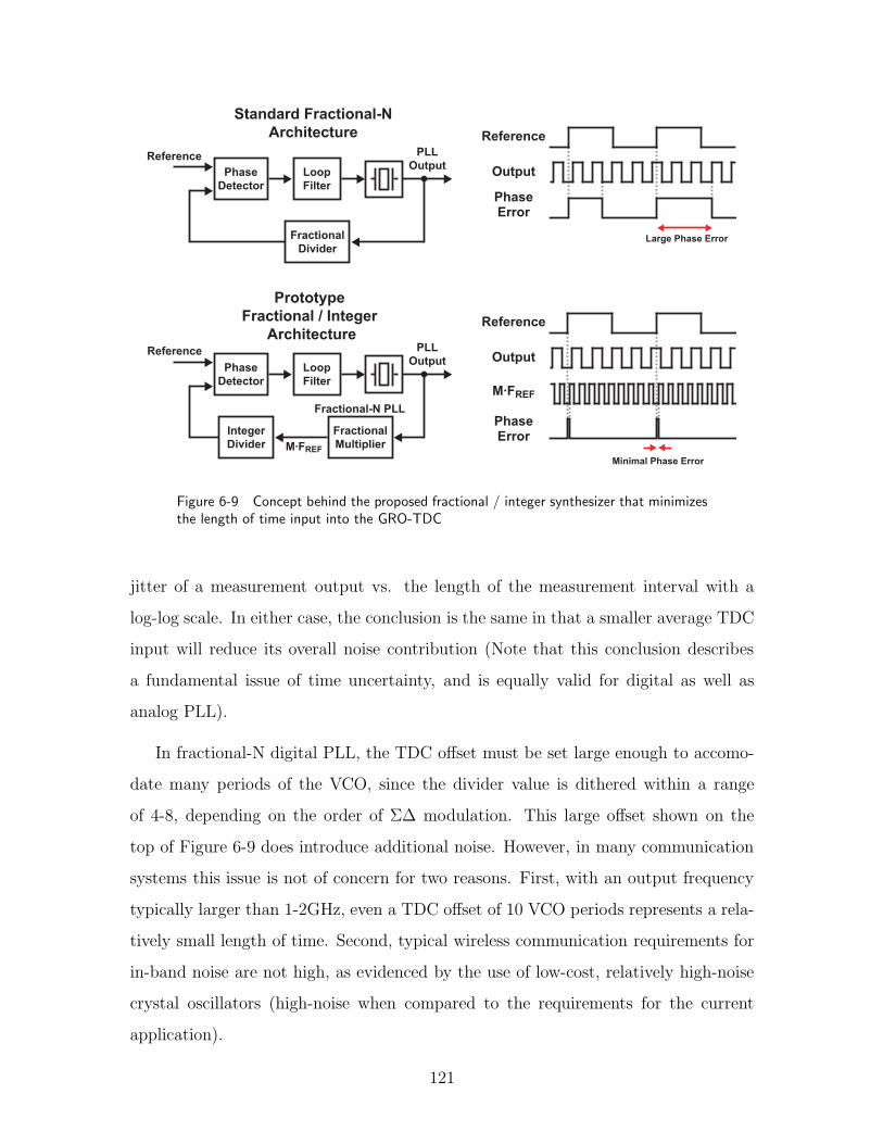
Prototype
Fractional / Integer
Architecture
Phase
Detector
Reference PLL
OutputLoop
Filter
Integer
Divider
Fractional
Multiplier
Fractional-N PLL
M.FREF
Output
Reference
M.FREF
PhaseError
Minimal Phase Error
Standard Fractional-N
Architecture
Phase
Detector
Reference PLL
OutputLoop
Filter
Fractional
Divider
Output
Reference
PhaseError
Large Phase Error
Figure 6-9 Concept behind the proposed fractional / integer synthesizer that minimizesthe length of time input into the GRO-TDC
jitter of a measurement output vs. the length of the measurement interval with a
log-log scale. In either case, the conclusion is the same in that a smaller average TDC
input will reduce its overall noise contribution (Note that this conclusion describes
a fundamental issue of time uncertainty, and is equally valid for digital as well as
analog PLL).
In fractional-N digital PLL, the TDC offset must be set large enough to accomo-
date many periods of the VCO, since the divider value is dithered within a range
of 4-8, depending on the order of Σ∆ modulation. This large offset shown on the
top of Figure 6-9 does introduce additional noise. However, in many communication
systems this issue is not of concern for two reasons. First, with an output frequency
typically larger than 1-2GHz, even a TDC offset of 10 VCO periods represents a rela-
tively small length of time. Second, typical wireless communication requirements for
in-band noise are not high, as evidenced by the use of low-cost, relatively high-noise
crystal oscillators (high-noise when compared to the requirements for the current
application).
121

Fractional
Divider
Digital
Loop Filter
Fractional
Frequency
(~3.6GHz)
DCO
GRO
TDC
ReferenceOutputFPGA-based
Loop Filter
Integer
Divider
Fractional-N PLL
DAC
Analog
Filter
GRO
TDC
100MHz
Crystal
Oscillator
Figure 6-10 Prototype implementation of the fractional / integer synthesizer
For synchronizing a 100MHz crystal to a timing reference with even lower fre-
quency with the lowest possible noise, it is clear that a classical fractional-N architec-
ture is non-optimal. To achieve a much smaller average TDC input, as shown on the
bottom of Figure 6-9, we instead propose a fractional / integer PLL architecture. In
this architecture a fractional divider is implemented by first multiplying the 100MHz
crystal output with a fractional-N digital PLL, and then following with an integer
division. Although there are two GRO-TDC in the signal path, which may intuitively
imply a larger noise, the sum of TDC input widths here is much smaller than in a
classic fractional-N topology. Specifically, the fractional-N GRO-TDC sees an average
input of less than 2ns, and the primary loop phase error can be maintained at a very
small value because the frequency of the feedback signal is synchronized to be equal
the reference frequency.
A prototype of this fractional / integer PLL synthesizer shown in Figure 6-10 is
implemented by combining the fractional-N synthesizer in [25] with a custom PCB
that includes a multi-path GRO-TDC [69], an FPGA-based loop filter, a DAC, ampli-
fication, and a single-pole passive RC filter. The digital IIR loop filter is programmed
in the FPGA with three taps using bit-shift operations to simplify the loop filter
multiplications, since the precision is 64-bit. Although the bit-shift multiplications
122

100
101
102
103
104
105
106
107
-180
-160
-140
-120
-100
-80
-60
-40
Offset Frequency (Hz)
Ph
ase N
ois
e (
dB
c/H
z)
98MHz Reference
100MHz PLL Output
Figure 6-11 Measured 100MHz phase noise of the prototype fractional / integer syn-thesizer
limit the ability to arbitrarily define the loop dynamics, issues such as settling time
and loop bandwidth are somewhat flexible in this application.
A 98MHz, fixed-frequency, temperature-regulated, quartz crystal oscillator is used
as the timing reference frequency, and a tunable 100MHz oscillator with the same
characteristics is used for the output frequency. The tuning gain of the 100MHz
oscillator, Kv, is about 500Hz/V. Both crystal oscillators are manufactured and pro-
vided by Frequency Electronics, Inc.
Measured phase noise performance for both the 98MHz timing reference as well
as the 100MHz synchronized output are shown in Figure 6-11. The overall PLL has
Type-II dynamics, and has a loop bandwidth for this measurement set approximately
to 10Hz. Although the entire loop filter can be implemented in discrete-time, due to
the more relaxed size and cost requirements there is little penalty in this application
for including a coarse RC analog filter with a pole at about 100Hz to attenuate spurs
and noise from the FPGA and DAC. As seen in the measured data, all noise outside
the frequency range of 10-300Hz is limited by the crystal oscillators, and a peak
deviation from the crystal noise is about 10dB for frequencies of 50-100Hz.
123
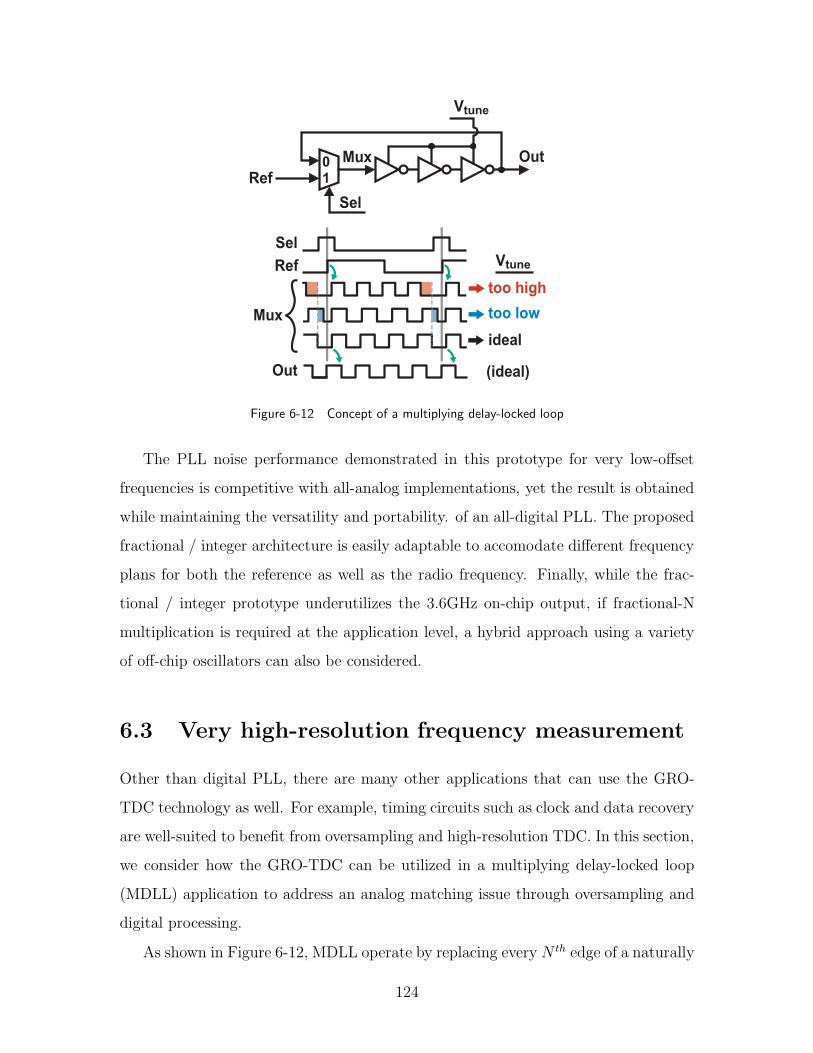
Vtune
0 1 Ref
OutMux
Ref
Sel
too low
too high
ideal
Mux
Vtune
Sel
Out (ideal)
Figure 6-12 Concept of a multiplying delay-locked loop
The PLL noise performance demonstrated in this prototype for very low-offset
frequencies is competitive with all-analog implementations, yet the result is obtained
while maintaining the versatility and portability. of an all-digital PLL. The proposed
fractional / integer architecture is easily adaptable to accomodate different frequency
plans for both the reference as well as the radio frequency. Finally, while the frac-
tional / integer prototype underutilizes the 3.6GHz on-chip output, if fractional-N
multiplication is required at the application level, a hybrid approach using a variety
of off-chip oscillators can also be considered.
6.3 Very high-resolution frequency measurement
Other than digital PLL, there are many other applications that can use the GRO-
TDC technology as well. For example, timing circuits such as clock and data recovery
are well-suited to benefit from oversampling and high-resolution TDC. In this section,
we consider how the GRO-TDC can be utilized in a multiplying delay-locked loop
(MDLL) application to address an analog matching issue through oversampling and
digital processing.
As shown in Figure 6-12, MDLL operate by replacing every N th edge of a naturally
124

MDLL Output
TDC Enable
T+∆T
T+∆T
∆
TDC Output
Correlation ∆
T+∆ T T+∆ T
∆
Figure 6-13 Correlation of spurs to period measurements
running ring oscillator VCO with a reference frequency edge, where N corresponds
to the frequency multiplication factor. This has been shown to allow significant
suppression of jitter caused by phase noise of the VCO [2]. However, as shown in
the figure, an incorrect setting of the Vtune voltage on the VCO (which tunes its
corresponding frequency) leads to substantial undesired “deterministic jitter” due to
corresponding periodic changes in the output period [1-2, 4-6].
Because elimination of this deterministic jitter is quite challenging in the analog
domain due to mismatch [4,5], an alternate approach is proposed in [21] that uses the
GRO-TDC to measure and compensate for this error. With the approach illustrated
in Figure 6-13, only one signal is examined, Enable, whose pulse width alternates
twice every reference cycle between the free running period of the oscillator, T , and
the period of the error-affected cycle, T + ∆. By doing a relative comparison of each
consecutive pulse period of the Enable signal, the value of ∆ can be obtained in a
manner such that the issue of mismatch is greatly mitigated since only one signal is
being examined.
The overall MDLL prototype, which is shown in simplified form in Figure 6-14,
consists of two integrated chips, a GRO-TDC chip and another with the MDLL
core logic, an FPGA board that implements the correlator, accumulator, a first-
125

Vtune
0 1 Ref
Out
Sel
Mux
Select
Logic
Enable
Logic Enable
Correlator DACGRO
2
RC Filt.
FPGA
50 MHz1.6 GHz
Accum Σ−∆
GRO IC MDLL Core IC
Div2x
NDiv
Div2x
Figure 6-14 A block diagram of the implemented MDLL prototype
Figure 6-15 Measured -58dBc spurious performance from the MDLL prototype
order, digital Σ∆ modulator, and other basic logic operations, an off-chip, low noise,
100MHz reference source, and a commercially available 16-bit DAC. While 16-bits
are available for the DAC, only 8-bits are used in conjunction with a first order Σ∆
modulator. Notice that again in this architecture, the key elements are the GRO-
TDC, a custom oscillator, a DAC, and some digital logic, which highlights how a
high-performance TDC can be leveraged for multiple applications by adding a small
number of new components.
126
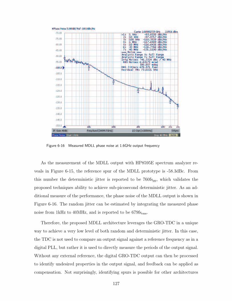
Figure 6-16 Measured MDLL phase noise at 1.6GHz output frequency
As the measurement of the MDLL output with HP8595E spectrum analyzer re-
veals in Figure 6-15, the reference spur of the MDLL prototype is -58.3dBc. From
this number the deterministic jitter is reported to be 760fspp, which validates the
proposed techniques ability to achieve sub-picosecond deterministic jitter. As an ad-
ditional measure of the performance, the phase noise of the MDLL output is shown in
Figure 6-16. The random jitter can be estimated by integrating the measured phase
noise from 1kHz to 40MHz, and is reported to be 679fsrms.
Therefore, the proposed MDLL architecture leverages the GRO-TDC in a unique
way to achieve a very low level of both random and deterministic jitter. In this case,
the TDC is not used to compare an output signal against a reference frequency as in a
digital PLL, but rather it is used to directly measure the periods of the output signal.
Without any external reference, the digital GRO-TDC output can then be processed
to identify undesired properties in the output signal, and feedback can be applied as
compensation. Not surprisingly, identifying spurs is possible for other architectures
127
as well (e.g. pulse injection-locked oscillators [22]), and the digital processing can
easily be modified to compensate for other spectral content as well. In fact, given
the high-resolution TDC now available as a tool for designers, this general technique
appears to be very promising for a wide variety of future system architectures.
128

Chapter 7
Background on VCO-based
quantizers
High-bandwidth and high-resolution ADC implementations face many challenges for
circuit designers using nanometer-scale CMOS processes, and yet the demand for
ADC performance is unrelenting. With limited power supply voltages and decreasing
gain for the minimum size transistors, achieving large dynamic range for high speed
converters is difficult for classical architectures that rely on precision operational
amplifiers and comparators. At the same time, advanced CMOS processes offer very
fast switching speed and high transistor density that can be utilized in interesting
and unconventional ways.
VCO-based quantization carries the very attractive aspect of having a highly
digital implementation, and as a result these structures strongly take advantage
of Moore’s law and the enormous industrial investment in digital process develop-
ment. Reducing the digital gate delay improves both the resolution of the VCO-
based quantizer as well as the achievable sample rate; a 9dB improvement in signal-
to-quantization noise results from a 50% reduction in gate delay. As such, there
has been an increasing level of interest in using VCO-based quantization to achieve
analog-to-digital conversion (ADC) in modern mixed-signal circuits [1, 28, 31, 39, 45].
However, one challenge for VCO-based quantizers is to mitigate the poor linearity
that can severely limit ADC performance.
129

Figure 7-1 Simple VCO-based ADC
To address such issues from an architectural perspective, in the following chapters
we explore the use of a multi-phase voltage-controlled oscillator (VCO) as a quantizer
element in oversampling continuous time (CT) ADC.
7.1 Common VCO-quantizer implementations
One of the earliest reported VCO-based ADC was proposed more than thirty years
ago for use in a digitally controlled switching regulator [5], and a similar topology
was later applied in the superconductivity community five years later [26]. While the
exact implementation of the converters differed due to the choice of technology (i.e.,
semiconductor vs. superconductor), the overall architecture for each was essentially
the same, and is shown in Figure 7-1. Here, the ADC comprises a single-phase output
VCO, a counter, and a sampling register. As the analog input signal modulates
the VCO frequency via the tuning node, the counter continuously accumulates the
number of transitioning edges during the sample period. At the end of the period,
the resulting count is sampled by a register, the counter reset to zero, and the process
repeated. As can be seen from the figure, the sampled count is proportional to the
oscillation frequency of the VCO, and therefore the input signal level.
One very interesting aspect of VCO-based quantizers is their potential ability to
achieve first-order noise-shaping of their quantization noise [24]. Figure 7-2 illustrates
this principle in simplified form by examining the counting process of one phase of the
130

Clock
Oscillator
Count
Out 3 3 4 3
Errorq[0] q[1] q[2] q[3]
-q[0] -q[1] -q[2] -q[3]
Vtune
Figure 7-2 First-order noise shaping of a classical VCO-based ADC
oscillator with a constant Vtune input. The key point here is that the truncation error
q[k] at the end of a clock period boundary is not lost, but rather it is accounted for in
the following measurement. The accumulation of phase error from sample to sample
is then maintained to within a single quantization level, which leads to a time-varying
output even with a constant input. This is shown in the figure by the extra count in
the third sample of the sequence [3 3 4 3]. Examination of the quantization error
signal, Error , in the figure reveals that it takes the form
Error [k] = q[k] − q[k − 1], (7.1)
where q[k] corresponds to the truncation error that occurs at the edge of each clock
period boundary. Under the assumption that q[k] is white in its noise profile, Equa-
tion 7.1 reveals that the overall quantization error is first-order noise-shaped.
The oscillator-based ADC of Figure 7-1 and 7-2 can be related to the well-known
slope-based converter (single or dual slope) [64] in that both architectures translate
an input voltage signal into the time-domain, where it is then quantized. However,
we make a key distinction that the single-slope ADC effectively compares an input
signal to an integrating waveform, while the VCO-based quantizer actually integrates
131

Ring Oscillator
Register
Reset
Count
Out
Ref
Count
Out 15 30
Vtune
12 21
Counters
OscillatorPhases
Vtune
Clock
Figure 7-3 Improved resolution by counting positive and negative transitions of a multi-phase VCO
the input signal in continuous time. As a result, the slope-based ADC lacks noise
shaping, and is not well-suited for oversampling applications. In fact, the linear
tradeoff between sampling rate and dynamic range limit the slope-based Nyquist
converters to high-resolution applications only when a very low input bandwidth is
desired. Regardless, the many variations on these time-based circuits for ultra low-
power sensor applications highlight the efficiency of combining voltage or current
integration with digital clocks [14, 33, 73, 75].
To improve the raw resolution of the VCO-based quantizer, the VCO needs to
generate more edge transitions during the sample period. This can be accomplished
by adopting a ring-oscillator structure to generate N multiple VCO output phases,
as proposed in [24] and shown in Figure 7-3. Here, each positive and negative phase
output from the ring-VCO drives a counter input, producing a total count with higher
resolution by a factor of 2N compared to the single-phase VCO-based ADC of [5,26]
for the same period.
Although the VCO-based quantizer shown in Figure 7-3 provides a convenient
illustration of the basic principles involved, its practical implementation is problem-
atic due to the reset operation that is used on its counters. Indeed, in cases where
a VCO edge occurs in close proximity to the reset signal (which will occur quite of-
ten), the measured edge count is likely to become corrupted due to the propagation
132
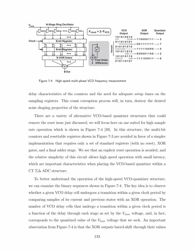
N-Stage Ring OscillatorVtune
Clock N-bit Register
N-bit Register
N XOR Gates
Out
z-1
First Order
Difference
Fclock > 2 FVCO VCO
Output
XOR
Output
Sa
mp
le
1 0 1 0 1 0 0 1 0
0 1 1 0 1 0 1 0 1
0 1 0 1 0 1 0 1 0
1 0 1 0 1 1 0 1 0
1 0 1 0 1 0 1 1 0
0 1 0 1 1 0 1 0 1
1 1 0 0 0 0 1 1 1
0 0 1 1 1 1 1 1 1
1 1 1 1 1 0 0 0 0
0 0 0 0 0 1 1 0 0
1 1 1 1 0 0 0 1 1
5
7
5
2
6
Quantizer
Output
Figure 7-4 High-speed multi-phase VCO frequency measurement
delay characteristics of the counters and the need for adequate setup times on the
sampling registers. This count corruption process will, in turn, destroy the desired
noise shaping properties of the structure.
There are a variety of alternative VCO-based quantizer structures that could
remove the reset issue just discussed; we will focus here on one suited for high sample
rate operation which is shown in Figure 7-4 [39]. In this structure, the multi-bit
counters and resettable registers shown in Figure 7-3 are avoided in favor of a simpler
implementation that requires only a set of standard registers (with no reset), XOR
gates, and a final adder stage. We see that an explicit reset operation is avoided, and
the relative simplicity of this circuit allows high speed operation with small latency,
which are important characteristics when placing the VCO-based quantizer within a
CT Σ∆ ADC structure.
To better understand the operation of the high-speed VCO-quantizer structure,
we can examine the binary sequences shown in Figure 7-4. The key idea is to observe
whether a given VCO delay cell undergoes a transition within a given clock period by
comparing samples of its current and previous states with an XOR operation. The
number of VCO delay cells that undergo a transition within a given clock period is
a function of the delay through each stage as set by the Vtune voltage, and, in fact,
corresponds to the quantized value of the Vtune voltage that we seek. An important
observation from Figure 7-4 is that the XOR outputs barrel-shift through their values
133

with each progressing sample. This property will be exploited later in this chapter.
A key constraint for achieving proper operation of the VCO-based quantizer in
Figure 7-4 is that the maximum number of VCO delay cell transitions that occur in
one clock period cannot exceed the number of stages N in the ring oscillator. We
express this restriction mathematically as
Ts
min Tdelay (V )< N, (7.2)
where Tdelay (V ) is the propagation delay of each delay stage as a function of VCO
tuning voltage, and Ts is the sampling period. Since the oscillator period, Tvco,
corresponds to the time it takes a given edge to propagate through each delay stage
twice, we also have
Tvco (V ) = 2NTdelay (V ) . (7.3)
By combining Equations 7.2 and 7.3, we can offer alternative views of the same
restriction to be that
min Tvco (V ) > 2Ts, (7.4)
max Fvco (V ) < Fs/2, (7.5)
where Fvco (V ) corresponds to the instantaneous frequency (in Hz) of the oscillator and
Fs = 1/Ts corresponds to the frequency (in Hz) of the sampling clock. Equation 7.5
therefore states that the maximum oscillator frequency should be confined to be less
than half of the quantizer clock frequency. If we assume that the nominal oscillator
frequency, Fvco, is half of its maximum value (such that half of the elements transition
for zero input), then we are left with requiring a sampling rate that is four times the
nominal VCO frequency. Thus, we have another design constraint that
Fs ≈2
N · Tdelay, (7.6)
where Tdelay is the nominal delay for each oscillator stage.
134

VCO
1- z-1
Quantizer
First Order
Difference
Clock
Vtune Out 2πKv
s1- z-1
Ts
1
Ts
Vtune Out
VCO Sampler
VCO
Noise
Quantization
Noise
First Order
Difference
ff
-20 dB/dec
Output
Noise
f
20 dB/dec
Figure 7-5 Block diagram model and corresponding linearized frequency domain modelof the VCO-based quantizer
7.2 SNDR limitations for VCO-based quantization
In this section we examine the key limitations in achieving high SNDR for VCO-
based quantizers. We begin with a linear model of the VCO-based quantizer to
provide a basis for the rest of this chapter, and then examine the theoretical limits to
SNR considering only quantization noise. A behavioral simulation example is then
presented which indicates the approximate SNDR performance of such quantizers in
0.13µm CMOS technology. The example will draw out the fact that non-linearity in
VCO-based quantization is the primary bottleneck to achieving high SNDR values.
7.2.1 Linear modeling
Figure 7-5 depicts a functional block diagram of the VCO-based quantizer on the left,
and its corresponding linearized frequency domain model on the right. Comparing the
block diagram to the corresponding quantizer structure in Figure 7-4, the VCO block
corresponds to the ring oscillator and the Quantizer block corresponds to the first set
of registers which sample the quantized phase signal of the VCO. The First Order
Difference block corresponds to comparison of the register values to their previous
sample values by the XOR gates in Figure 7-4. In the corresponding frequency domain
model, the VCO is represented as an integrator with gain 2πKv, which represents
conversion of the Vtune voltage to a VCO phase signal, and the addition of phase
noise. The Quantizer is modeled as a sampler that adds quantization noise, and the
135

First Order Difference block is seen as a 1 − z−1 transfer function that performs a
discrete-time differentiation.
A key observation offered by Figure 7-5 is that the quantization noise is first-order
noise-shaped by virtue of the first order difference operation shown in the figure,
which is in agreement with the time domain view of the quantization noise described
in Equation 7.1. We also see that the VCO phase noise is shaped as well, but the
result of such shaping is a flat spectrum due to the -20 dB/dec slope of the original
phase noise signal. In reality, the shaped VCO phase noise will also include 1/f noise,
but this is ignored for now for the sake of modeling simplicity.
In effect, the First Order Difference block converts the VCO phase signal to a
corresponding VCO frequency signal. To be precise, however, the discrete-time (DT)
differentiation is not an exact inverse function of the continuous-time (CT) integra-
tion, noting first that sampling will alias the input signal, and that the 1− z−1 filter
is only an approximation to the CT differentiation. As shown in Figure 7-6(a), the
resulting DT spectrum of the VCO frequency measurement tightly follows the input
spectrum for low frequencies with the expected low-frequency gain factor of 2πKv,
but then begins to fall off slightly around Fs/2 (Ω = π) due to the CT/DT inverse
approximation.
An interesting observation to be made here is that the VCO-based quantizer has
an inherent first-order anti-alias filter. This can be seen in the quantizer output on
the right side of Figure 7-6(a) by comparing the reconstructed input signal (shown
as a dark line) with the aliased copy (shown with a lighter shade). Although by itself
this first-order anti-alias filter can be considered as fairly crude, the aliasing rejection
approximately equal to 20 log (Fs/Fb) can be significant for some applications. Here,
Fb refers to the analog input bandwidth.
For purposes of linear analysis it can be useful to choose a primary time domain
in which to operate, and for historical reasons we choose here to use discrete time.
Therefore, we next will develop a DT model for the VCO-quantizer that will be helpful
later in this chapter. First, it is commonly known that the DT accumulation can be
136
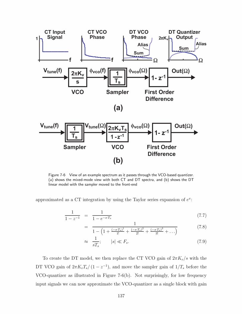
2πKvTs
2πKv
s1- z-1
1
Ts
Vtune(f)
VCO Sampler First Order
Difference
CT InputSignal
f
φvco(f) φvco(Ω)
CT VCOPhase
f
DT VCOPhase
Ω
DT QuantizerOutput
Ω
Alias Alias
SumSum
Vtune(Ω)
VCO First Order
Difference
φvco(Ω)
(a)
(b)
1 2πKv
Out(Ω)
Out(Ω)1
Ts
Sampler
1 - z-1 1- z-1
Vtune(f)
Figure 7-6 View of an example spectrum as it passes through the VCO-based quantizer.(a) shows the mixed-mode view with both CT and DT spectra, and (b) shows the DTlinear model with the sampler moved to the front-end
approximated as a CT integration by using the Taylor series expansion of ex:
1
1 − z−1=
1
1 − e−s·Ts(7.7)
=1
1 −(
1 + (−s·Ts)1
1!+ (−s·Ts)
2
2!+ (−s·Ts)
3
3!+ . . .
) (7.8)
≈1
sTs
; |s| Fs. (7.9)
To create the DT model, we then replace the CT VCO gain of 2πKv/s with the
DT VCO gain of 2πKvTs/ (1 − z−1), and move the sampler gain of 1/Ts before the
VCO-quantizer as illustrated in Figure 7-6(b). Not surprisingly, for low frequency
input signals we can now approximate the VCO-quantizer as a single block with gain
137

Avco−q(z) that translates an input voltage Vtune(z) to a frequency (in rad/sample) at
the VCO output Out(z) by
Avco−q(z) =Out(z)
Vtune(z)≈ 2πKvTs [rad/sample/V]; ω Fs. (7.10)
7.2.2 Theoretical SNR
Now that a model for the VCO quantizer has been described, we can utilize the
well-established analysis of oversampling quantizers in order to provide a theoretical
bound to its SNR performance. The expression for peak signal-to-quantization noise
ratio (SQNR) of a Σ∆ converter is found in [17] to be
SQNRpeak =3π
2·(
2β − 1)2
· (2n + 1) ·(
OSR
π
)2n+1
(7.11)
where β is the number of bits, n is the Σ∆ order, and the oversampling ratio OSR =
Fs/(2Fb). For the first-order VCO-based quantizer, with Tdelay and Fs as the primary
design variables related to N through Equation 7.6, we have
2β − 1 = N =2
Fs · Tdelay. (7.12)
Therefore, we can simplify Equation 7.11 to
SQNRpeak =9
4π2(Fb)3
Fs
(Tdelay)2. (7.13)
One important thing to notice from Equation 7.13 is that SQNRpeak of the VCO-
based quantizer improves independently with both faster sampling and faster delay
elements. For a series connected ring oscillator, the nominal delay per stage is set to
be approximately twice the minimum inverter delay in the process, and the sampling
rate is set to be as large as practical. Thus, advancing the process to reduce the digital
delay by a factor of 2 can improve SQNRpeak by 9dB for the same input bandwidth.
138

2π
s1- z-1
1
Ts
Vtune Out
Frequency
to Phase
Sampler
VCO
Noise
Quantization
Noise
First Order
Difference
ff
Output
Spectrum
f
Tuning
Gain
Input
Harmonics
f
Input
Spectrum
f
Kv
Figure 7-7 Behavioral model illustrating the VCO quantizer non-linearity
7.3 Example
The previous subsections highlighted quantization noise and, to a lesser extent, ther-
mal noise as key non-idealities of the VCO-quantizer. However, one important issue
that has so far been neglected is that the voltage-to-frequency tuning curve of a VCO
is quite non-linear in practice. Figure 7-7 shows that the impact of such non-linearity
is to introduce harmonic distortion which can significantly degrade the SNDR per-
formance of the quantizer. Although the linear models so far provide an intuitive
understanding of the VCO-quantizer, we will now see that the VCO non-linearity is
actually a critical bottleneck to achieving good SNDR performance when this quan-
tizer is used for analog-to-digital conversion.
To gain a better idea of the relative limitations posed by each of these nonideal-
ities, we now present an example design of a VCO-based quantizer. Considering a
0.13µm CMOS process technology, along with typical noise and non-linearity perfor-
mance, we choose to make the following assumptions for the design example:
• Sampling clock: Fs = 1GHz,
• Nominal delay per stage: Tdelay = 65psec,
• Nominal VCO gain: Kv = 750MHz/V,
139

105
106
107
108
Frequency (Hz)
Example VCO-quantizer Output Spectrum
Quantization
Noise
Nonlinearity
Thermal
Noise
0
-100
-60
-40
-20
Am
pli
tud
e (
dB
)-80
-120
-140
Figure 7-8 Behavioral simulation results of an example VCO-based quantizer
• Non-linearity of VCO tuning characteristic: ±10%,
• VCO Noise: -100dBc/Hz at 1MHz offset.
From Equation 7.6, the above choice of sampling frequency and delay implies that N
= 31 and that Fvco = 250MHz. The Kv of 750MHz/V then restricts the maximum
input signal to be ±300mV.
Figure 7-8 displays the impact of the three key nonidealities on the quantizer
output spectrum given a 2.5MHz input signal near full-scale. The figure illustrates
first order noise shaping of the quantization noise, filling in of the low frequency noise
by the VCO phase noise, and harmonic distortion caused by the non-linear VCO
tuning characteristic.
In this example, let us choose to lowpass filter the quantizer output with a band-
width Fb set to 20MHz, which coincides with the point at which the influence of
quantization noise is comparable to that of the VCO phase noise. In such a situation,
we obtain the following SNDR values:
• Quantization noise only: 68dB1,
1Note that the behavioral simulation with only quantization noise agrees with the theoreticalcalculation from Equation 7.13 (page 138)
140

• Quantization noise and VCO phase noise: 65dB,
• Quantization noise, VCO phase noise, and non-linearity: 34dB (SQNRpeak =
50dB)
This example clearly reveals that VCO non-linearity forms the primary bottleneck
to achieving high SNDR values for the VCO-based quantizer. It is this issue that leads
us to the Σ∆ ADC architecture presented in the next chapter.
141

142

Chapter 8
VCO-based quantizer Σ∆ ADC
Architecture
One approach to improving a quantizer’s linearity and quantization noise performance
is to place the quantizer in a Σ∆ feedback loop. It is natural to consider the VCO-
based quantizer for a Σ∆ ADC [28, 39], since its distortion and quantization errors
will be suppressed by the preceding gain of the loop filter. A general block diagram
for such an architecture is shown in Figure 8-1, which shows exaggerated waveforms
to illustrate the loop limiting the effect of VCO non-linearity.
There are many differences between the VCO-based quantizer and a traditional
comparator-based FLASH quantizer in the context of a Σ∆ ADC. For example, we
will see a unique attribute of the VCO-based quantizer architecture is that the overall
quantization noise shaping is the sum of the first-order shaping from the VCO-based
quantizer plus the order of the loop dynamics. Other differences between the quantiz-
ers are that a VCO-based quantizer inherently provides dynamic element matching
(DEM), lower probability of metastable behavior, less sensitivity to offset and mis-
match, and signal-dependent power compsumption.
In the second part of this chapter, we define a model for the VCO-based quan-
tizer Σ∆ ADC including non-linearity error that allows for analysis of non-linearity
suppression. This model will verify that the VCO-based quantizer Σ∆ ADC does
indeed have an extra order of quantization noise-shaping, and also will highlight the
143

VCO-based
Quantizer
Gain and
Filtering
Clock
DAC
In OutVtune
DAC Out
Error
Figure 8-1 Σ∆ feedback to suppress VCO linearity and quantization errors
fact that many traditional techniques for reducing quantization noise also apply to
suppressing VCO-based quantizer non-linearity. Last, we confirm the model with
behavioral simulation of two idealized converters.
8.1 Comparison of VCO-based quantizer and comparator-
based FLASH quantizer for Σ∆ ADC
Compared with a stand-alone quantizer, the specific application of a high-bandwidth
CT Σ∆ converter stresses a unique set of quantizer performance requirements. There-
fore, in this section, we examine a few of the key differences between the VCO-based
quantizer and the classical comparator-based FLASH quantizer in the context of a
high-speed CT Σ∆ ADC.
8.1.1 Implicit Barrel-Shift DEM using the VCO-based quan-
tizer
A main attraction to high-speed CT Σ∆ ADC is the ability to leverage very high-
speed sampling in order to maximize input bandwidth and dynamic range. However,
for high-speed, multi-bit Σ∆ ADC (>500Msps and >2-bit), a very significant design
challenge is to implement a DEM algorithm for the feedback DAC elements within
strict timing requirements and with minimal power consumption. Although many dy-
144

VCO-based
Quantizer
Gain and
Filtering
Clock
DAC
In Out
N-Stage Ring OscillatorVtune
ClockN-bit Register
N-bit Register
N XOR Gates
DAC Out
Vtune
DAC Out
1-Bit DACs
Implicit
Barrel-Shift
DEM
Barrel-Shift DEM
Qu
an
tizer
Ele
men
t
Sample
Figure 8-2 Utilizing VCO for implicit barrel shift DEM of DAC elements
namic element matching (DEM) techniques are well known, many approaches become
overly complex for many levels or are not suitable for clocking at very high-speed.
Fortunately, the multi-bit VCO-based quantizer can implement a barrel-shift DEM
algorithm without any penalty in terms of latency or power, which is a significant
advantage of the architecture.
Figure 8-2 illustrates how by connecting the outputs of the VCO-based quantizer
to the DAC elements in a bit-wise fashion, the phase rotation of the VCO inherently
implements the barrel-shift DEM algorithm [39]. Instead of digitally summing the
XOR outputs prior to the feedback DAC, an analog summation is accomplished with
current after the DAC. The first element to be used in a sample period is the last
one left over from the previous sample, which ensures that each element is used with
equal likelihood. To generate the output word, digital adders are still required, but
these may be pipelined as the delay has been removed from the critical path.
We should note that some very demanding applications have avoided use of the
barrel-shift algorithm due to the potential for tones created by limit-cycles in the
signal band. This issue is a valid concern, as will be seen in Chapter 10, although the
level of degradation can be considered to be negligable for the vast majority of appli-
cations. Compared to the comparator-based quantizer, which has no inherent DEM
145
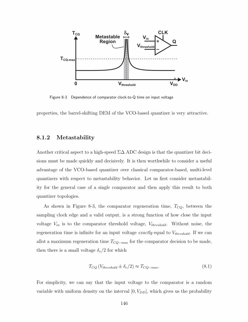
TCQ-max
MetastableRegion
δvTCQ
VinVthreshold
QVin
Vthreshold
CLK
0 VDD
Figure 8-3 Dependence of comparator clock-to-Q time on input voltage
properties, the barrel-shifting DEM of the VCO-based quantizer is very attractive.
8.1.2 Metastability
Another critical aspect to a high-speed Σ∆ ADC design is that the quantizer bit deci-
sions must be made quickly and decisively. It is then worthwhile to consider a useful
advantage of the VCO-based quantizer over classical comparator-based, multi-level
quantizers with respect to metastability behavior. Let us first consider metastabil-
ity for the general case of a single comparator and then apply this result to both
quantizer topologies.
As shown in Figure 8-3, the comparator regeneration time, TCQ, between the
sampling clock edge and a valid output, is a strong function of how close the input
voltage Vin is to the comparator threshold voltage, Vthreshold. Without noise, the
regeneration time is infinite for an input voltage exactly equal to Vthreshold. If we can
allot a maximum regeneration time TCQ−max for the comparator decision to be made,
then there is a small voltage δv/2 for which
TCQ (Vthreshold ± δv/2) ≈ TCQ−max. (8.1)
For simplicity, we can say that the input voltage to the comparator is a random
variable with uniform density on the interval [0, VDD], which gives us the probability
146
of metastability in a single comparator to be
Pcomp [metastability] = Pcomp [Vin | TCQ (Vin) > TCQ−max] ≈δv
VDD. (8.2)
In an ideal FLASH ADC, the input voltage interval [0, VDD] is uniformly divided
into N subintervals, each with a unique threshold voltage centered on the subinterval.
Let us assume that for a single input only one comparator has an input signal close
to its threshold, which gives the probability of metastability for the FLASH ADC of
Pflash [metastability] = Pflash [Vin | TCQ (Vin) > TCQ−max] ≈Nδv
VDD. (8.3)
As can be seen in Equation 8.3, the probability of a metastable event increases
linearly with the number of quantization levels in the flash ADC for the same com-
parator. To compensate, regenerative amplifiers (or pipelined latches) must be put
in front of the comparators in order to effectively reduce δv. Unfortunately, such
improvements inevitably coming at the price of increased power consumption and
area.
In the case of the VCO-based quantizer, we first note that the input voltages to
the comparators are primarily binary voltage signals saturated to either 0 or VDD.
When the VCO is a ring oscillator comprising of a serial chain of inverters, only one of
the outputs is transitioning between these binary levels at a time. As such, when we
consider the input voltage distribution of the comparators only one of them will see
a uniform distribution at a time. Therefore, the overall probability of metastability
for the VCO-based quantizer is the same as the single comparator, or explicity
Pvco [metastability] = Pcomp [TCQ > TCQ−max] ≈δv
VDD. (8.4)
To compare, the probability of a metastable event for an arbiter used in the
VCO-based quantizer is approximately a factor of N smaller than when used in a
FLASH architecture, and it is also independent of the number of quantization levels.
This result simplifies the VCO-based quantizer comparator design and allows for very
147
high-speed operation with minimal power consumption.
8.1.3 Comparator Offset and Monotonicity
Since most high-speed comparators designs utilize minimum-size devices, offset in
deep sub-micron comparators can be 50mV or more. For a multi-bit FLASH ADC,
this level of comparator offset can be on the order of a quantization step size, which
introduces significant non-linearity and threatens quantizer monotonicity. Although
this would be a concern for any converter, in Σ∆ ADC these issues can cause the
loop to severely limit-cycle or even become unstable. Consequently, some form of
offset calibration is needed in the implementation of a traditional multi-bit FLASH
quantizer.
When we consider how comparator offset affects the VCO-based quantizer, we
first recognize that the level of comparator offset is much smaller than a quantization
step size. Using an argument similar to that discussed above for metastability, the
quantization step size is effectively equal to VDD, which can be argued will always be
much smaller than a comparator offset. Second, we also recognize that the quantiza-
tion error due to comparator offset will be first-order shaped. To explain, recall that
in the same barrel-shifting manner discussed earlier for the DAC DEM circuit, the
use of comparators and their associated offsets are rotated as the VCO rising/falling
edge propagates around the ring.
Given these results, it is not surprising that the VCO-based quantizer is also
guaranteed to be statistically monotonic, and in fact, it is relatively easy to prove this
additional property. Equation 7.10 (Avco−q ≈ 2πKvTs) states that the VCO acts as a
simple gain element at DC, and thus mapping an input voltage to output frequency
is one-to-one and monotonic. Due to the ideal integration and differentiation in the
VCO-based quantizer at DC, the measurement or quantization error in determining
the DC output frequency limits to zero. We can then conclude that, even in the
presence of large comparator offsets, the DC transfer function from analog input
voltage to digital output is monotonic.
148

8.1.4 Power Supply Considerations
One final issue to consider in the design of high resolution ADC is the correlation
between the input signal and power consumption, either through digital switching or
analog biasing. If such power supply variation or noise non-linearly couples into the
signal path, distortion in the actual conversion can result. For the multi-bit FLASH
quantizer, each of the comparators switches for each sample, and so to first-order the
quantizer power consumption does not depend on the input signal. For the VCO-
based quantizer, the switching activity within the VCO core is directly proportional to
the input signal, and as such the power supply current is a relatively strong function
of the input signal. As such, care must be taken to properly isolate the VCO power
supply from other analog blocks in the signal path.
8.2 Modeling the suppression of VCO-based quan-
tizer non-linearity
While we hypothesized earlier that feedback with high gain will improve the VCO
non-linearity, a more quantitative examination of the non-linearity suppression can
be useful in highlighting the fundamental tradeoffs and limitations of the technique.
Figure 8-4 shows a simplified DT and CT model for a basic Σ∆ VCO-based ADC
that includes error terms from both a quantization error, Eq, and also a VCO non-
linearity error, Enl. Although each domain has advantages for different stages of the
ADC design, as mentioned earlier we will use DT from this point forward, without
loss of generality. In this model the units of Eq are [rad], and the units of Enl are
[rad/sample], which normalizes the non-linearity error to the reference frequency.
As the quantization noise-transfer function Hq describes how the quantization
error Eq is shaped in the digital output of the ADC, we can also consider a non-
linearity transfer function Hnl that will suppress the non-linearity error Enl from the
VCO-based quantizer. For this analysis we make a small-signal linear approximation
that allows us to define an input signal Enl(z) that is decoupled from U(z), allowing
149

Alf(z) 1 - z-1
U(Ω) V(Ω)
LoopFilter
PhaseIntegrator
First OrderDifference
1 - z-1
Enl(Ω) Eq(Ω)
Avco-q
VCOTuningGain
1
Ts
Sampler
U(f) 1
Adac
DAC
Alf(s) sV(Ω)V(f)
LoopFilter
PhaseIntegrator
First OrderDifference
s
Enl(f) Eq(f)
Avco-q
VCOTuningGain
1
Ts
Sampler
U(f) 1
Adac
DAC
(a)
(b)
Figure 8-4 A model in discrete-time (a) and continuous-time (b) for the VCO-basedquantizer Σ∆ ADC with non-linearity error Enl and quantization error Eq
us to estimate how well the loop is able to reject Enl(z) as a function of frequency.
With these definitions, we can generally describe the modulator output V (z) as
V (z) = G(z)U(z) + Hq(z)Eq(z) + Hnl(z)Enl(z). (8.5)
From Figure 8-4 we find that
G(z) = Avco−qAlf (z)H(z), (8.6)
Hnl(z) = H(z), (8.7)
Hq(z) =(
1 − z−1)
H(z), (8.8)
150
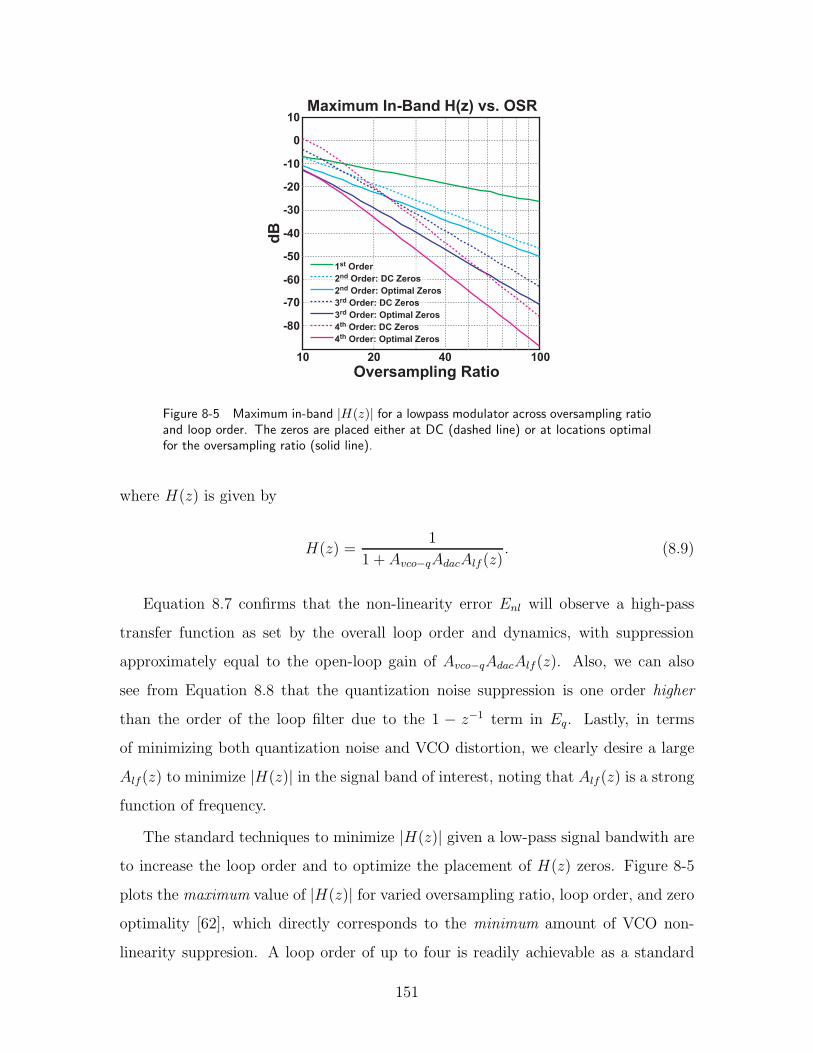
10 100
-80
-70
-60
-50
-40
-30
-20
-10
0
10
Oversampling Ratio
dB
Maximum In-Band H(z) vs. OSR
1st Order
2nd Order: DC Zeros
4020
2nd Order: Optimal Zeros
3rd Order: DC Zeros
3rd Order: Optimal Zeros
4th Order: DC Zeros
4th Order: Optimal Zeros
Figure 8-5 Maximum in-band |H(z)| for a lowpass modulator across oversampling ratioand loop order. The zeros are placed either at DC (dashed line) or at locations optimalfor the oversampling ratio (solid line).
where H(z) is given by
H(z) =1
1 + Avco−qAdacAlf (z). (8.9)
Equation 8.7 confirms that the non-linearity error Enl will observe a high-pass
transfer function as set by the overall loop order and dynamics, with suppression
approximately equal to the open-loop gain of Avco−qAdacAlf(z). Also, we can also
see from Equation 8.8 that the quantization noise suppression is one order higher
than the order of the loop filter due to the 1 − z−1 term in Eq. Lastly, in terms
of minimizing both quantization noise and VCO distortion, we clearly desire a large
Alf(z) to minimize |H(z)| in the signal band of interest, noting that Alf(z) is a strong
function of frequency.
The standard techniques to minimize |H(z)| given a low-pass signal bandwith are
to increase the loop order and to optimize the placement of H(z) zeros. Figure 8-5
plots the maximum value of |H(z)| for varied oversampling ratio, loop order, and zero
optimality [62], which directly corresponds to the minimum amount of VCO non-
linearity suppresion. A loop order of up to four is readily achievable as a standard
151
practice today, and in this case a large oversampling ratio (OSR) provides tremendous
supression of VCO nonlinearity error. However, as the OSR decreases to less than
20, for stability reasons the various loop orders begin to cluster together. In fact,
if the OSR < 16, the higher order loops lose so much advantage that a first-order
loop is actually preferable to a fourth-order loop without optimal zero-placement.
Therefore, applications with larger OSR will especially benefit from the advantages
of the VCO-based quantizer.
We can now make a few general observations regarding the suppression of VCO
non-linearity from Σ∆ feedback. In one sense, the Σ∆ modulator has improved the
VCO-based quantizer nonlinearity by approximately the gain of the loop, which is a
significant and marked advance compared to the stand-alone architecture. However,
we can also see that the linearity performance of the VCO has not been improved in
relation to the quantization noise. Observe that both the quantization noise Eq(z)
and the distortion Enl(z) have been modified by the same factor of H(z) compared
to the quantizer without feedback. Therefore, as was the case in the VCO-based
quantizer example from Section II, we may expect that the VCO non-linearity may
still present a limitation for frequencies very close to the maximum edge of the input
bandwidth.
8.3 Example
To verify the above analysis, we can again simulate an example VCO-based quantizer
Σ∆ ADC at the behavioral level using CppSim [50], a very-fast code-driven C++
simulator that is especially targeted at high-performance mixed-signal systems. A
tutorial that includes the example simulation is also free and available online.
Before simulating the converter from Figure 8-4, we first need to consider that,
even in the ideal sense, the VCO-based quantizer has a delay that has so far not been
modeled. This excess loop delay causes phase lag in the signal transfer function, and
must be accounted for in order to ensure loop stability. For our purposes here, the
delay for the VCO-based quantizer is approximated by a single sample period. As we
152
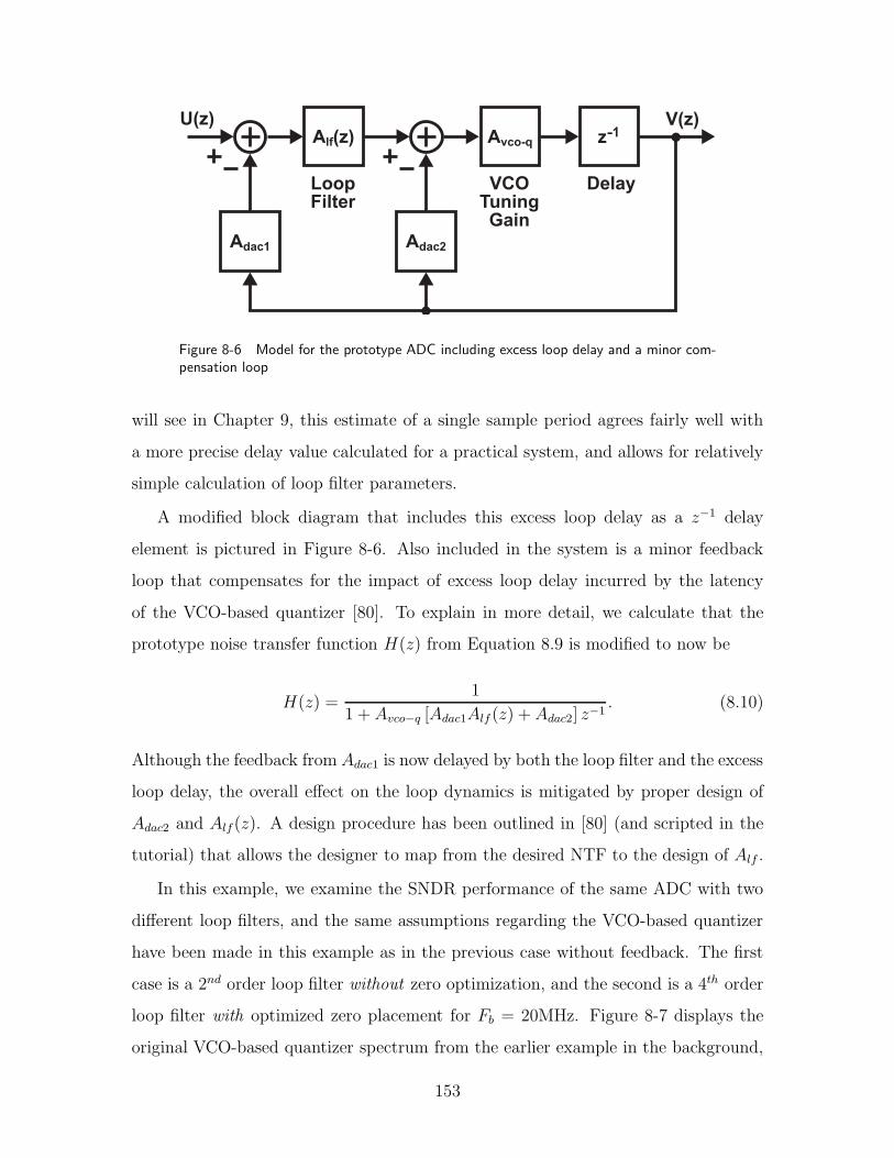
Alf(z)U(z) V(z)
LoopFilter
Avco-q
VCOTuningGain
Adac1 Adac2
z-1
Delay
Figure 8-6 Model for the prototype ADC including excess loop delay and a minor com-pensation loop
will see in Chapter 9, this estimate of a single sample period agrees fairly well with
a more precise delay value calculated for a practical system, and allows for relatively
simple calculation of loop filter parameters.
A modified block diagram that includes this excess loop delay as a z−1 delay
element is pictured in Figure 8-6. Also included in the system is a minor feedback
loop that compensates for the impact of excess loop delay incurred by the latency
of the VCO-based quantizer [80]. To explain in more detail, we calculate that the
prototype noise transfer function H(z) from Equation 8.9 is modified to now be
H(z) =1
1 + Avco−q [Adac1Alf (z) + Adac2] z−1. (8.10)
Although the feedback from Adac1 is now delayed by both the loop filter and the excess
loop delay, the overall effect on the loop dynamics is mitigated by proper design of
Adac2 and Alf(z). A design procedure has been outlined in [80] (and scripted in the
tutorial) that allows the designer to map from the desired NTF to the design of Alf .
In this example, we examine the SNDR performance of the same ADC with two
different loop filters, and the same assumptions regarding the VCO-based quantizer
have been made in this example as in the previous case without feedback. The first
case is a 2nd order loop filter without zero optimization, and the second is a 4th order
loop filter with optimized zero placement for Fb = 20MHz. Figure 8-7 displays the
original VCO-based quantizer spectrum from the earlier example in the background,
153

Example Σ∆ ADC Output Spectrum
105
106
107
108
0
-160
-120
-80
-40
Frequency (Hz)
Am
pli
tud
e (
dB
)
105
106
107
108
0
-160
-120
-80
-40
Am
pli
tud
e (
dB
)
SNR = 99.5dB
SNDR = 93.7dB
SNR = 86.6dB
SNDR = 77.4dB
Frequency (Hz)
(a) (b)
Open-loop VCO-quantizer
2nd order
loop filter4th order
loop filter
Fb Fb
Figure 8-7 Behavioral simulation results of an example VCO-based quantizer Σ∆ ADCwith (a) 2nd order loop filter with NTF zeros at DC and (b) 4th order loop filter withoptimized zeros for Fb = 20MHz
and overlays the spectrum of the Σ∆ ADC in the foreground. The first case with a
2nd order loop filter is shown on the left side in Figure 8-7 (a), and one can clearly
see that the suppression of both the quantization noise and non-linearity decreases
with frequency, as expected. On the right side in Figure 8-7 (b) is the second case
with a 4th order loop filter with optimized zeros. Here, the level of error suppression
is significantly increased, and the suppression is generally flatter across the band of
interest. Note that the “white” noise in Figure 8-7 (b) is not quantization error, but
rather it is believed to be a error from quantization effects.
By comparing the simulation results of the two loop filters, we can justify the
assumptions made previously in developing the model for non-linearity suppression.
In fact, both the levels of suppression as well as the overall frequency dependence
agree with what would be expected from the model. In practice, however, there
are many other potential sources of non-linearity in these very high-speed Σ∆ ADC
(e.g. DAC mismatch, front-end amplifier distortion), and these other errors must be
balanced not only against the VCO-based quantizer non-linearity, but also against
thermal and 1/f noise.
154

8.4 Conclusion
This chapter has compared the use of the VCO-based quantizer to the traditional
FLASH based architecture, and found that the VCO-based quantizer offers a few
unique advantages such as the ability to provide inherent dynamic element matching,
as well as reduced sensitivity to metastability and comparator offset. The primary
issue with the VCO-based quantizer, the linearity of its voltage-to-frequency tuning
characteristic, has been modeled within a Σ∆ ADC and we have seen that for large
open-loop gains, the linearity performance can be improved significantly. Finally, the
model was substantiated with simulation examples, illustrating that while the VCO
non-linearity has indeed been suppressed by the gain of the preceding loop filter, it
may yet pose a limitation for overall converter distortion performance.
155

156

Chapter 9
Prototype Σ∆ ADC with a
VCO-quantizer
In this section we demonstrate a prototype Σ∆ ADC that is able to significantly
suppress VCO-quantizer non-linearity, achieve third-order noise shaping with a single
op-amp, and provide inherent dynamic element matching for the feedback DAC. We
will discuss the prototype architecture, detail the design of primary circuit blocks,
and then show measurement results.
9.1 Σ∆ ADC Architecture
Figure 9-1 displays our proposed ADC structure. This circuit topology incorporates
an active loop filter, two 31-element current DACs, and a 31-level VCO-based quan-
tizer to achieve third order noise shaping. One should immediately notice the simplic-
ity offered by this structure — the active analog components consist of just one opamp,
two current DACs, and a ring oscillator (within the VCO-based quantizer). Indeed,
the simplicity allows high-speed sampling at 950Mz to be achieved with compact
area and low power dissipation. Note that while a single-ended schematic is shown
for clarity, the ADC is fully differential with the exception of a pseudo-differential
VCO-quantizer, as will soon be discussed in more detail.
While the topology shown in Figure 9-1 bears resemblance to the popular second-
157
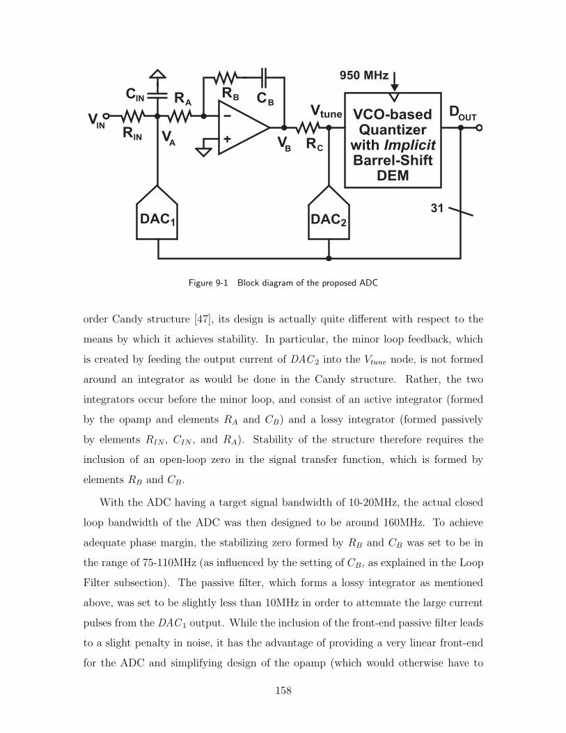
DOUTV
IN
950 MHz
Vtune
VA V
B
VCO-based Quantizer
with Implicit Barrel-Shift
DEM
31
RC
RB CBRACIN
RIN
DAC1 DAC2
Figure 9-1 Block diagram of the proposed ADC
order Candy structure [47], its design is actually quite different with respect to the
means by which it achieves stability. In particular, the minor loop feedback, which
is created by feeding the output current of DAC 2 into the Vtune node, is not formed
around an integrator as would be done in the Candy structure. Rather, the two
integrators occur before the minor loop, and consist of an active integrator (formed
by the opamp and elements RA and CB) and a lossy integrator (formed passively
by elements RIN , CIN , and RA). Stability of the structure therefore requires the
inclusion of an open-loop zero in the signal transfer function, which is formed by
elements RB and CB.
With the ADC having a target signal bandwidth of 10-20MHz, the actual closed
loop bandwidth of the ADC was then designed to be around 160MHz. To achieve
adequate phase margin, the stabilizing zero formed by RB and CB was set to be in
the range of 75-110MHz (as influenced by the setting of CB, as explained in the Loop
Filter subsection). The passive filter, which forms a lossy integrator as mentioned
above, was set to be slightly less than 10MHz in order to attenuate the large current
pulses from the DAC 1 output. While the inclusion of the front-end passive filter leads
to a slight penalty in noise, it has the advantage of providing a very linear front-end
for the ADC and simplifying design of the opamp (which would otherwise have to
158

deal more directly with the current pulses of DAC 1).
As opposed to optimizing the zeros of the ADC noise transfer function for a
signal bandwidth of 10-20MHz, we chose to implement a simple ADC topology that
highlights the properties of the VCO-based quantizer. Additionally, the chosen topol-
ogy allows for second-order dynamics and third-order noise shaping with only a single
opamp. To explain, the proposed topology achieves third-order noise shaping through
the inclusion of three zeros within its quantization noise transfer function, Eq, as ex-
plained earlier. Two of those zeros, as provided by the VCO-quantizer and the active
integrator, are located at or very near the origin. The third zero, as provided by
the lossy integrator formed by the front-end passive filter, is located slightly below
10MHz as set by the bandwidth of that filter.
While the choice of 10-20MHz signal bandwidth did not explicitly influence the
zero placement, it was strongly considered in choosing appropriate thermal noise levels
for the opamp, DAC 1, and the front-end passive filter. These blocks were therefore
designed such that the overall thermal noise had a comparable spectral density to the
quantization noise at the edge of the signal bandwidth range (i.e., 20MHz).
Given the above overview of the proposed structure, we now examine its various
blocks in detail in the subsections to follow. In particular, we will present additional
circuit details of the VCO-based quantizer, the current DACs, and the loop filter.
9.2 Circuit Implementation
9.2.1 VCO-based quantizer
Figure 9-2 illustrates a geometric view of the combined VCO-based quantizer, implicit
DEM, and DAC circuitry implemented with 31 levels. In essence, this structure cor-
responds to the VCO-based quantizer shown in Figure 7-4 which has been augmented
with DAC elements. A bit-slice of this structure, which is also shown in the figure,
reveals a variable delay consisting of a 4-transistor stack followed by a buffer, some
digital logic to implement the first order difference operation, and a DAC element
159

I
D Q
Lesstransitionswith small
input
Vtune / Vtune
D Q
1-bit IDACslice
IOUT
950 MHz
Variabledelay
QuantizingRegister
1-z-1
Differentiator
CurrentDAC
out / Iout
Moretransitionswith large
input
7-10x
1x
1x
Vtune Vtune
7-10x
Figure 9-2 Geometric view of the proposed 31-level combined VCO quantizer/DEM andDAC
with current output. The buffer is used to isolate the variable delay output from
the sampling register, which is implemented with standard cell regenerative latches.
Simulations demonstrated that metastability is not a concern, as predicted from the
discussion in Section 8.1.2. In terms of delay timing, a half-period is available before
generating the DAC pulses, which allows use of standard cell XOR gates and TSPC
DFF for the subsequent first-order difference logic.
There are several advantages of implementing the variable delay element as a
complementary 4-transistor stack. First, the pseudo-differential control of the delay
value provides a seamless interface with the output of a fully differential loop filter
circuit so that common-mode noise in that path is rejected. Second, the topology
provides reasonably good linearity in the voltage-to-frequency tuning characteristic
of the VCO with a compact and low-power implementation, and allows a very large
frequency tuning range for the VCO needed to achieve a high range of quantization
levels. Third, full-swing CMOS logic levels in the delay element are directly compat-
ible with the standard cell regenerative latches used for the phase register. Last, the
structure supports a high clock rate by achieving a small minimum delay of 35-40ps
in the 0.13µm CMOS process, which is comparable to a loaded inverted delay in that
160
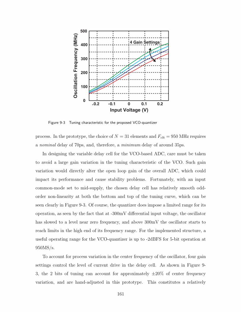
-0.2 -0.1 0 0.1 0.20
100
200
300
400
500
Input Voltage (V)
Os
cil
lati
on
Fre
qu
en
cy
(M
Hz)
4 Gain Settings
Figure 9-3 Tuning characteristic for the proposed VCO-quantizer
process. In the prototype, the choice of N = 31 elements and Fclk = 950 MHz requires
a nominal delay of 70ps, and, therefore, a minimum delay of around 35ps.
In designing the variable delay cell for the VCO-based ADC, care must be taken
to avoid a large gain variation in the tuning characteristic of the VCO. Such gain
variation would directly alter the open loop gain of the overall ADC, which could
impact its performance and cause stability problems. Fortunately, with an input
common-mode set to mid-supply, the chosen delay cell has relatively smooth odd-
order non-linearity at both the bottom and top of the tuning curve, which can be
seen clearly in Figure 9-3. Of course, the quantizer does impose a limited range for its
operation, as seen by the fact that at -300mV differential input voltage, the oscillator
has slowed to a level near zero frequency, and above 300mV the oscillator starts to
reach limits in the high end of its frequency range. For the implemented structure, a
useful operating range for the VCO-quantizer is up to -2dBFS for 5-bit operation at
950MS/s.
To account for process variation in the center frequency of the oscillator, four gain
settings control the level of current drive in the delay cell. As shown in Figure 9-
3, the 2 bits of tuning can account for approximately ±20% of center frequency
variation, and are hand-adjusted in this prototype. This constitutes a relatively
161

coarse adjustment of the frequency offset of the VCO tuning characteristic, which
is acceptable since any remaining offset simply translates into a differential offset
voltage at the input of the VCO tuning port. Of course, in the case of a severe offset,
linearity performance will suffer and, ultimately, the open loop gain of the ADC will
significantly drop if frequency saturation occurs in the VCO. Note that the impact of
power supply and thermal variations on the oscillator center frequency are mitigated
by the feedback having large gain at low frequency, as will be seen in Chapter 10.
Finally, since excess delay introduced by the quantizer degrades the phase margin
of the ADC structure, it is worthwhile to estimate its value in the proposed VCO-
based quantizer structure. To do so, note that Vtune is integrated over the previous
sampling period which can be seen as a 1/2 clock delay, and the DAC 1 pulse logic
begins 1/2 period after the quantizer positive sampling edge. Additionally, there is
an estimate of 1/4 clock delay for generating the RZ DAC pulses. The combination
of these effects leads to an excess loop delay of approximately 1.25 clock periods.
9.2.2 DAC
An RZ topology was chosen for the primary DAC in the prototype ADC (i.e., DAC 1
in Figure 9-1) in order to minimize the impact of inter-symbol interference at the
high sample frequency of 950MHz and to provide additional compensation of excess
loop delay introduced by the VCO-based quantizer. The penalties for choosing an RZ
topology are larger current variation at the output summing node, increased sensitiv-
ity to clock jitter, and increased power [80]. As mentioned earlier, the issue of current
variation was addressed through the use of passive filtering in the prototype. The is-
sue of clock jitter, which strongly impacts the SNR of any high-speed continuous-time
Σ∆ ADC structure, was addressed by using a low noise, off-chip clocking source. The
issue of power consumption was partially mitigated through circuit design efforts, the
details of which are described below.
The schematic for the primary RZ DAC element core is shown in part (a) of Fig-
ure 9-4, and the overall DAC structure comprises of 31 unit elements, each connected
bit-wise to the VCO-quantizer outputs. Degenerated transistors with moderate chan-
162

VA-
VP2
VN1
VN2
DAC Element
(1 of 31)
VP1
VSS
VSS
VDD
DATA = 0
DATA = -1
DATA = 1
IP
IN
VDD
VA+ VOFF
Figure 9-4 Schematic and operation of (a) DAC 1 and (b) DAC 2
nel lengths (and accompanying cascode devices) are used on both the top and bottom
current sources to minimize thermal and 1/f noise. The output common mode range
of the DAC is set via the low impedance of the input signals, which have a common
mode voltage of half-supply (VDD/2). Large, off-chip capacitors are used for both the
NMOS and PMOS bias voltages to reduce the noise coupling from the current refer-
ence. The full-scale on current of DAC 1 is ±9 mA, which corresponds to a full-scale
input current of ±4.5 mA.
As shown in Figure 9-4 (a), a triple-source configuration steers the current bias
to either the positive or negative summing node during the active pulse, and to a
relatively low impedance node set at VDD/2 during the return-to-zero time. This
configuration allows the current sources to share current during the RZ time, and
163
therefore saves 25% of the current compared with alternative topologies. However,
there is still 50% more bias current used in this design than would be for an NRZ
implementation.
The RZ DAC switching waveforms are at full-level CMOS logic levels, so the
switching transistors see a large overdrive. The on pulse control is output from
NAND gates which retimes the data with the negative clock state. Careful attention
to balancing the differential signals helps to keep source bounce low during switching
events. Again, the power required in generating the switching waveforms for the RZ
implementation is significantly higher than for an NRZ DAC, especially considering
the 950MHz sampling rate.
In contrast to the RZ approach used for the primary DAC, the minor loop DAC
(which corresponds to DAC 2 in Figure 9-1) is implemented as an NRZ structure due
to its less stringent performance requirements. The clocking of this DAC is done
without retiming since the sensitivity to clock jitter and ISI is suppressed by the
forward integration path. The 31-elements of this second DAC are scrambled with
the barrel-shift DEM due to the bit-wise connection to the VCO-based quantizer,
though the issue of DAC mismatch is not as important for this DAC as the primary
one. The full-scale current of DAC 2 is nominally ±64 µA, and can be adjusted over a
wide range through an off-chip bias current such that peaking is properly controlled
in the noise transfer function (NTF) of the ADC. With the minor loop disabled by
removing the DAC current bias, the ADC was found to still be marginally stable.
9.2.3 Loop filter
The fully-differential loop filter schematic, which uses only a single opamp, is shown
in Figure 9-5. As mentioned earlier, the loop filter includes a front-end passive fil-
ter composed of elements RIN , RA, and CIN in order to absorb the large current
deviations of DAC 1 and provide a very linear ADC front-end. Closer examination
of the front-end passive filter reveals that voltage VA is actually a virtual ground
when placed in Σ∆ feedback, so the ADC input current IIN is defined primarily by
resistor RIN . The capacitor CIN then filters the error signal IIN − IDAC1 before IA
164

VINVA
RIN
CIN
RA
RBCB
RC
Vtune
IDAC1
IDAC1
IDAC2
IDAC2
Figure 9-5 Schematic of the fully differential ADC loop filter
VP1
VSS
VDD
Vin-Vin+
Vout-Vout+
VP2
VN1
VCMFB
Figure 9-6 Operational amplifier schematic
is integrated onto capacitor CB, whose value can be adjusted by ±25% with an on-
chip binary capacitor array. Adjustment of CB leads to a gain change in the active
integrator, which allows for better accomodation of Kv variations in the VCO-based
quantizer. Of course, changes in CB will also lead to variation in the value of the
open loop zero formed by CB and RB.
The loop filter opamp is implemented with the two-stage Miller-compensated
topology shown in Figure 9-6. Since the ADC input is assumed to have a constant
165
common-mode voltage at its input, the first opamp stage can be cascoded even with
low supply voltage. Note that the output common-mode voltage also controls the
input common-mode of the VCO, and is set according to a common-mode feedback
circuit that consists of two large polysilicon resistors, a single-stage amplifier, and
an off-chip reference voltage [58]. Interestingly, because the VCO-based quantizer
offers relatively high SNR performance on its own, a large DC open loop gain is not
required for the opamp in the proposed ADC topology. As such, the gain is designed
to be over 50dB with a gain-bandwidth product in the range of 2-3GHz.
As mentioned earlier, minor loop feedback is used to compensate for excess loop
delay from the quantizer and DAC 1 in order to allow a more aggressive NTF. To avoid
the use of another amplifier for a summation operation, current DAC 2 is directed
through resistor RC such that the resulting voltage is added to the output of the
opamp. Although the opamp output resistance is non-zero, it is much less than RC
in the frequencies of interest and does not need to be well-controlled since the gain
and precision of this minor loop is not critical to ADC performance. The value of RC
is chosen to keep the parasitic pole, which is formed by RC and the input capacitance
of the quantizer, from affecting the loop dynamics. The full scale current of DAC 2
is then set based on the value of RC and considerations of the NTF. In addition to
providing analog summation without an amplifier, another benefit to this topology
is that the stability concerns of the operational amplifier are isolated from the input
capacitance of the VCO-based quantizer.
166

Chapter 10
Σ∆ ADC results and discussion
A prototype of the ADC structure shown in Figure 9-1 is implemented in a 0.13µm CMOS
process. A microphotograph of the fabricated chip is shown in Figure 10-1. The ac-
tive silicon area of the ADC is 640µm×660µm, including power supply decoupling
capacitors and guardring. Area for the 5-bit VCO-quantizer core is 120µm×86µm,
and the total chip area including 28 pads is 1.3mm x 1.3mm.
10.1 Measurement setup
The ADC chip is direct bonded onto an FR-4 circuit board that provides control
signals, biasing, and power supplies with adequate decoupling capacitors. The out-
put of the ADC is implemented with full-swing digital inverters on-chip, however a
series resistor is included both on and off-chip, and termination is provided by a low
impedance resistive network biased at mid-supply to minimize voltage swings.
To capture the 5-bits of 1Gsps data from the ADC, a pair of 4-channel digital
oscilloscopes with a sample rate of 5Gsps are triggered to collect 1Msamples simulta-
neously. Because 3-bits are sampled on the first instrument and 2-bits on the second,
the data is then downloaded to MATLAB where clock and data recovery is performed
digitally. For collecting parametric data measurements, a MATLAB interface controls
the triggering, oscilloscopes, and data analysis.
Synchronized low-noise signal sources are used for both the input signal and sam-
167
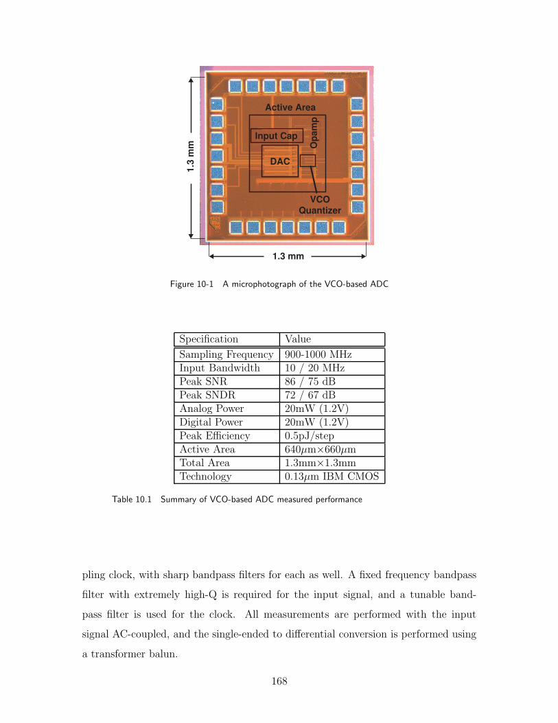
1.3 mm
1.3
mm
Active Area
VCOQuantizer
DAC
Input Cap
Op
am
p
Figure 10-1 A microphotograph of the VCO-based ADC
Specification Value
Sampling Frequency 900-1000 MHzInput Bandwidth 10 / 20 MHzPeak SNR 86 / 75 dBPeak SNDR 72 / 67 dBAnalog Power 20mW (1.2V)Digital Power 20mW (1.2V)Peak Efficiency 0.5pJ/stepActive Area 640µm×660µmTotal Area 1.3mm×1.3mmTechnology 0.13µm IBM CMOS
Table 10.1 Summary of VCO-based ADC measured performance
pling clock, with sharp bandpass filters for each as well. A fixed frequency bandpass
filter with extremely high-Q is required for the input signal, and a tunable band-
pass filter is used for the clock. All measurements are performed with the input
signal AC-coupled, and the single-ended to differential conversion is performed using
a transformer balun.
168

-100 -90 -80 -70 -60 -50 -40 -30 -20 -10 0
0
20
40
60
80
Variable Analog Bandwidth
Input Amplitude (dBFS)
dB
SNR
10
30
50
70
90
10, 15, 20 MHz
SNDR
-100 -90 -80 -70 -60 -50 -40 -30 -20 -10 0
0
20
40
60
80
Variable Input Frequency
Input Amplitude (dBFS)
dB
SNR
10
30
50
70
90
SNDR
1.0, 2.5, 5.0 MHz
-100 -90 -80 -70 -60 -50 -40 -30 -20 -10 0
0
20
40
60
80
Variable Sample Rate
Input Amplitude (dBFS)
dB
SNR
10
30
50
70
90
SNDR
FS = 900MHz
FS = 950MHz
FS = 1000MHz
-100 -90 -80 -70 -60 -50 -40 -30 -20 -10 0
0
20
40
60
80
Variable Supply Voltage
Input Amplitude (dBFS)
dB
SNR
10
30
50
70
90
SNDR
VDD = 1.2V
VDD = 1.3V
VDD = 1.4V
VDD = 1.5V
Figure 10-2 SNR/SNDR vs. input amplitude
10.2 Measurement results
The power consumption of the ADC is 40mW, which is evenly split between the 1.2V
analog and digital supplies such that each draw roughly 16-17mA. Although there
is no direct way to measure the sub-system current, bias currents indicate that the
primary DAC consumes 9mA, and the operational amplifier 8mA. For the digital
supply, the pulse waveform generation circuits for the RZ DAC require about 8mA,
the VCO-quantizer 5mA, and the thermometer-to-binary summation circuits take the
remaining 3mA. A summary of the ADC performance is found in Table 10.1, where
the figure of merit is Power/(2 · Bandwidth · 2ENOB).
The SNR and SNDR vs. input amplitude curves across a number of operating
169

conditions are shown in Figure 10-2. If not otherwise specified, the input frequency
is 2.5MHz, the analog bandwidth is 10MHz, and the sample rate is 950MHz. At
a 10MHz input bandwidth, the ADC achieves at least 81dB SNR and 65dB SNDR
across all input frequencies, a power supply of 1.2-1.5V, and a sampling frequency
of 900-1000MHz. While a peak SNR of 14-bits at 10MHz is achieved very efficiently
with only 40mW of total power consumption, the ADC distortion performance is
limited by the VCO-quantizer non-linearity to 10.5-12bits, depending on the specific
test configuration.
The decline of SNDR with increasing signal frequency in Figure 10-2 is a con-
sequence of the reduced gain of the loop filter at higher frequencies, which leads to
reduced suppression of the VCO non-linearity. The degradation of SNDR by such
non-linearity was about 5dB higher than predicted by simulation. This is likely due
to the modeling accuracy of the VCO tuning characteristic, which can be affected
by layout in addition to process and temperature variations. It may be possible to
improve the SNDR somewhat with more attention given to modeling these issues,
although as we will see later that other techniques offer more promise in improving
VCO linearity.
It was observed that low input signal levels into the proposed ADC led to small
limit-cycles which were seen in the 10-100kHz frequency range. These limit cycles are
an artifact of the barrel-shift algorithm used for DEM on the DACs, which is why some
demanding applications avoid the use of the barrel-shift algorithm in favor of other
DEM strategies [3]. These small limit-cycles can reduce the SNR by a few dB when
the input signal falls below about -35dBFS, as seen in the SNR vs. amplitude curves.
As would be expected, the actual frequency of the limit-cycle depends somewhat on
the input DC level.
An FFT of the ADC output with an 1.045MHz input signal at -15dBFS is shown
in Figure 10-3. The third-order noise shaping is visible from 10-50MHz, and the
quantization noise peaks around 60MHz. A small noise skirt centered around 1MHz
was found to be from the bandpass filter used in testing. The high frequency quanti-
zation noise feature occuring in the 200-300MHz range is believed to be caused by the
170

0.1 1 10 100 1000-80
-60
-40
-20
0
20
40
60
Frequency (MHz)
Am
pli
tud
e (
dB
)
Normalized FFT, FIN = 1 MHz
SNR
SNDR
76.2
72.4
10 MHzInput Bandwidth
65.7
66.4
20 MHz
Figure 10-3 190,190 point Hanning FFT normalized to an LSB
Ref.FS
(MHz)BW
(MHz)SNR(dB)
SNDR(dB)
Power(mW)
[79] 276 23 70 69 43[6] 340 20 71 69 56[49] 400 12 64 61 70[61] 640 10 72 66 7.5[40] 640 20 76 74 20[60] 1000 8 63 63 10
This work 950 10 86 72 40
Table 10.2 Comparison with published high-speed CT ADC
mismatch between rising and falling edges of the VCO-quantizer, as verified with be-
havioral simulation. Fortunately, this artifact does not affect the functional operation
of the ADC as its stability was seen to be robust across a wide variety of operating
conditions.
10.3 Discussion
Table 10.2 compares this work with other reported CT Σ∆ CMOS ADC operating
at a sampling rate over 250MHz and an analog bandwidth of more than 5MHz.
171

The high SNR of 86dB achieved in this work points to the strength of the VCO-
quantizer architecture, which allows efficient reduction of quantization noise through
high-speed operation. In addition, the SNDR performance and power consumption
are in line with other realizations, and as seen in Chapter 8, additional VCO non-
linearity suppression is possible to improve performance further.
In combination with an optimized NTF for a 10-20MHz bandwidth, a higher-order
loop filter may be expected to yield at least another 10dB or more of linearity on top
of the performance reported in this work. Coupled with a more power efficient NRZ
DAC design, a forecast performance of over 80dB with 20-30mW in 0.13µm CMOS
would certainly compete well with today’s state-of-the-art implementations and ar-
chitectures. Because the VCO-quantizer scales well with digital process technology,
there may be even more advantage in the architecture going forward.
Some ADC applications requiring more than 13-14 ENOB with low OSR may face
practical limitations to the levels of linearity suppression from that can be achieved
from known in-loop analog techniques reported in this work. In addition, other sources
of distortion will then become significant, both in the feedback DAC and in the front-
end amplifiers. Future research in the area of VCO-quantizers may find promising
results from novel Σ∆ linearization techniques, alternative ADC architectures with
less sensitivity to VCO voltage-to-frequency distortion, or operation with a more
balanced level of linearity and quantization noise performance.
172
Chapter 11
Conclusion
In this thesis, we have introduced, analyzed, and demonstrated a set of noise-shaping
techniques that utilize a voltage controlled ring oscillator in a variety of ways. These
techniques were applied to two distinct state-of-the-art converters, a time-to-digital
converter with first-order quantization and mismatch noise-shaping, and a continuous-
time Σ∆ analog-to-digital converter. In both cases, the fundamental ability of the
VCO to perform analog signal processing with highly digital circuitry was leveraged
to efficiently achieve high-performance data conversion in advanced CMOS.
For the VCO-based time-to-digital converter, a multi-path gated ring oscillator
topology was introduced that, when combined with appropriate measurement tech-
niques as discussed, can achieve first-order noise-shaping of quantization and mis-
match error. The key requirement of the architecture, to accurately preserve ana-
log state information, was discussed in detail, and two example GRO designs were
presented to highlight the important design considerations. First-order TDC noise-
shaping performance was then verified in a prototype implementation fabricated in
0.13µm CMOS technology, with measurements presented at both the component and
system level.
To our knowledge, the gated ring oscillator time-to-digital converter presented in
this thesis was the first TDC to demonstrate noise-shaping of analog quantization
and mismatch error for non-adjacent measurement intervals. Further, compared with
other reported TDC, the prototype described in this work is very competitive in
173

regard to important metrics such as dynamic range, power, and area.
In the case of the VCO-based analog-to-digital converter, the performance advan-
tages and limitations of a VCO-based quantizer were presented and discussed using
both theory and simulated examples. Because the non-linearity of the VCO fre-
quency tuning presents the primary bottleneck for achieving high-performance, trade-
offs for using the VCO-quantizer within a Σ∆ ADC architecture were presented. To
demonstrate these considerations, a high-speed continuous time Σ∆ ADC operating
at 950Msps was designed and fabricated in 0.13µm CMOS. Although the architecture
chosen for this work was originally disclosed in [39], measurement results were pre-
sented in this work that justifies the consideration of VCO-based quantizers in Σ∆
ADC. Possible improvements are also discussed that may significantly improve these
results.
Because analog device characteristics in future CMOS processes are not expected
to improve, the increasing trend of replacing analog signal processing with digital
signal processing is likely to continue. At the same time, analog functions cannot
entirely disappear from the mixed-signal interface. Therefore, as demonstrated in
this work, the ability to achieve and leverage high-performance analog functionality
with highly digital circuit elements is very compelling, and is an exciting area for
future research.
174

Bibliography
[1] E. Alon, V. Stojanovic, and M. Horowitz. Circuits and techniques for high-resolution measurement of on-chip power supply noise. IEEE Journal of Solid-State Circuits, 40:820–828, April 2005.
[2] Y. Arai, T. Matsumura, and K. Endo. A CMOS four-channel x 1 K time memoryLSI with 1-ns/b resolution. IEEE Journal of Solid-State Circuits, 27:359–364,March 1992.
[3] R. Baird and T. Fiez. Linearity enhancement of multibit deltasigma A/D andD/A converters using data weighted averaging. IEEE TCAS-II, 42:753–762,December 1995.
[4] R.G. Baron. The Vernier Time-Measuring Technique. Proceedings of the IRE,pages 21–30, January 1957.
[5] V. B. Boros. A Digital Proportional Integral and Derivative Feedback Controllerfor Power Conditioning Equipment. IEEE Power Electronics Specialists Conf.Rec., pages 135–141, June 1977.
[6] L. Breems, R. Rutten, R. van Veldhoven, G. van der Weide, and H. Termeer.A 56mW CT Quadrature Cascaded Σ∆ Modulator with 77dB DR in a NearZero-IF 20MHz Band. IEEE ISSCC, pages 238–239, February 2007.
[7] H.-H. Chang, P.-Y. Wang, J.-H.C. Zhan, and B.-Y. Hsieh. A fractionalspur-free ADPLL with loop-gain calibration and phase-noise cancellation forGSM/GPRS/EDGE. IEEE ISSCC Dig. Tech. Papers, pages 200–201, Febru-ary 2008.
[8] C.-C. Chen, P. Chen, C.-S. Hwang, and W. Chang. A Precise Cyclic CMOSTime-to-Digital Converter With Low Thermal Sensitivity. IEEE Trans. Nucl.Sci., 52:834–838, 2005.
[9] P. Chen, C.-C. Chen, and Y.-S. Shen. A Low-Cost Low-Power CMOS Time-to-Digital Converter Based on Pulse Stretching. IEEE Trans. Nucl. Sci., 53:2215–2220, 2006.
[10] P. Chen, J.-C. Zheng, and C.-C. Chen. A Monolithic Vernier-Based Time-to-Digital Converter with Dual PLLs for Self-Calibration. IEEE Custom IntegratedCircuits Conference, pages 321–324, 2005.
175

[11] J.-M. Chou, Y.-T. Hsieh, and J.-T. Wu. A 125 MHz 8b digital-to-phase converter.IEEE Int. Solid-State Circuits Conf., 2003.
[12] J.-M. Chou, Y.-T. Hsieh, and J.-T. Wu. Phase averaging and interpolation usingresistor strings or resistor rings for multi-phase clock generation. IEEE Trans.Circuits and Systems I, 53:984–991, 2006.
[13] P. Dudek, S. Szczepanski, and J. V. Hatfield. A high-resolution CMOS time-to digital converter utilizing a Vernier delay line. IEEE Journal of Solid-StateCircuits, 35:240–247, February 2000.
[14] M. A. Farahat, F. A. Farag, and H. A. Elsimary. Only digital technology analog-to-digital converter circuit. IEEE International Midwest Symposium on Circuitsand Systems, pages 178–181, December 2003.
[15] M. Ferriss and M.P. Flynn. A 14mW Fractional-N PLL Modulator with an En-hanced Digital Phase Detector and Frequency Switching Scheme. IEEE ISSCCDig. Tech. Papers, pages 352–353, February 2007.
[16] B.W. Garlepp, K.S. Donnelly, Jun Kim, P.S. Chau, J.L. Zerbe, C. Huang, C.V.Tran, C.L. Portmann, D. Stark, Yiu-Fai Chan, T.H. Lee, and M.A. Horowitz. Aportable digital DLL for high-speed CMOS interface circuits. IEEE Journal ofSolid-State Circuits, 34:632–644, 1999.
[17] Y. Geerts, M. Steyaert, and W. Sansen. Design of Multi-Bit Delta-Sigma A/DConverters. Kluwer Academic Publishers, 2002.
[18] E. J. Gerds, J. Van der Spiegel, R. Van Berg, H. H. Williams, L. Callewaert,W. Eyckmans, and W. Sansen. A CMOS time to digital converter IC with 2level analog CAM. IEEE Journal of Solid-State Circuits, 29:1068–1076, 1994.
[19] M.S. Gorbics, J. Kelly, K.M. Roberts, and R.L. Sumner. A high resolutionmultihit time to digital converter integrated circuit. IEEE Trans. Nucl. Sci.,44:379–384, 1997.
[20] A. Hajimiri, S. Limotyrakis, and T.H. Lee. Jitter and Phase Noise in RingOscillators. IEEE Journal of Solid-State Circuits, 34(6):790–804, June 1999.
[21] B. Helal, M. Straayer, and M. H. Perrott. A Low Jitter 1.6 GHz MultiplyingDLL Utilizing a Scrambling Time-to-Digital Converter and Digital Correlation.VLSI Symp. Dig. Tech. Papers, pages 166–167, June 2007.
[22] B. M. Helal, C.-M. Hsu, K. Johnson, and M. H. Perrott. A Low Noise Pro-grammable Clock Multiplier Based on A Pulse Injection-Locked Oscillator witha Highly-Digital Tuning Loop. IEEE RFIC Symp., June 2008.
[23] S. Henzler, S. Koeppe, W. Kamp, H Mulatz, and D. Schmitt-Landsiedel. 90nm4.7ps-Resolution 0.7-LSB Single-Shot Precision and 19pJ-per-Shot Local PassiveInterpolation Time-to-Digital Converter with On-Chip Characterization. IEEEInt. Solid-State Circuits Conf., pages 548–549, 2008.
176

[24] M. Hoven, A. Olsen, T. S. Lande, and C. Toumazou. Novel second-order Σ-∆modulator/frequency-to-digital converter. IEEE Electronics Letters, 31:81–82,January 1995.
[25] C. M. Hsu, M. Straayer, and M. H. Perrott. A Low Noise, Wide Bandwidth, 3.6-GHz Digital Σ∆ Fractional-N Frequency Synthesizer with Quantization NoiseCancellation. IEEE ISSCC Dig. Tech. Papers, page N/A, February 2008.
[26] J.P. Hurrell, D.C. Pridmore-Brown, and A.H. Silver. Analog-to-Digital Con-version with Unlatched SQUIDs. IEEE Transactions on Electron Devices, ED-27(10), 1980.
[27] C. S. Hwang, P. Chen, and H. W. Tsao. A high-precision time-to-digital converterusing a two-level conversion scheme. IEEE Trans. Nucl. Sci., 51(4):1349–1352,August 2004.
[28] A. Iwata. The architecture of delta sigma analog-to-digital converters using aVCO as a multibit quantizer. IEEE TCAS-II, 46:941–945, July 1999.
[29] J.-P. Jansson, A. Mantyniemi, and J. Kostamovaara. A CMOS Time-to-DigitalConverter With Better Than 10 ps Single-Shot Precision. IEEE Journal of Solid-State Circuits, 41:1286–1296, 2006.
[30] K. Karadamoglou, N. P. Paschalidis, E. Sarris, N. Stamatopoulos, G. Kottaras,and V. Paschalidis. An 11-bit high-resolution and adjustable range CMOS time-to-digital converter for space science instruments. IEEE Journal of Solid-StateCircuits, 39:214–222, 2004.
[31] J. Kim and S. Cho. A Time-Based Analog-to-Digital Converter Using a Multi-Phase VCO. IEEE ISCAS, pages 3934–3937, May 2006.
[32] S. Kleinfelder, T. Majors, K. Blumer, W. Farr, and B. Manor. MTD132-a newsub-nanosecond multi-hit CMOS time-to-digital converter. IEEE Trans. Nucl.Sci., 38:97–101, April 1992.
[33] F. Kocer and M.P. Flynn. A new transponder architecture with on-chip ADCfor long-range telemetry applications. IEEE JSSC, 41:557–564, May 2006.
[34] M. Lee and A.A. Abidi. A 9b, 1.25ps Resolution Coarse-Fine Time-to-DigitalConverter in 90nm CMOS that Amplifies a Time Residue. IEEE Journal ofSolid-State Circuits, 43:769–777, April 2008.
[35] S. J. Lee, B. Kim, and K Lee. A novel high-speed ring oscillator for multiphaseclock generation using negative skewed delay scheme. IEEE Journal of Solid-State Circuits, 32:289–291, February 1997.
[36] J. G. Maneatis and M. A. Horowitz. Precise delay generation using coupledoscillators. IEEE Journal of Solid-State Circuits, 28(12):1273–1282, December1993.
177

[37] A. Mantyniemi, T. Rahkonen, and J. Kostamovaara. An integrated 9-channeltime digitizer with 30 ps resolution. IEEE Int. Solid-State Circuit Conf., pages266–465, 2002.
[38] A. Matsumoto, S. Sakiyama, Y. Tokunaga, T. Morie, and S. Dosho. A De-sign Method and Developments of a Low-Power and High-Resolution MultiphaseGeneration System. IEEE Journal of Solid-State Circuits, 43:831–843, 2008.
[39] M. Miller. Multi-bit continuous time sigma-delta ADC. US Patent No. 6,700,520,2003.
[40] G. Mitteregger, C. Ebner, S. Mechnig, T. Blon, C. Holuigue, and E. Romani.A 20-mW 640-MHz CMOS Continuous-Time Σ∆ ADC With 20-MHz SignalBandwidth, 80-dB Dynamic Range and 12-bit ENOB. IEEE JSSC, 41:2641–2649, July 2004.
[41] S. S. Mohan, W. S. Chan, D. M. Colleran, S. F. Greenwood, J. E. Gamble, andI. G. Kouznetsov. Differential Ring Oscillators with Multipath Delay Stages.IEEE CICC, pages 503–506, September 2005.
[42] S.S. Mohan, W.S. Chan, D.M. Colleran, and S.F. Greenwood. Differential RingOscillators with Multipath Delay Stages. IEEE Custom Integrarted CircuitsConference, pages 503–506, September 2005.
[43] M. Mota and J. Christiansen. A high-resolution time interpolator based on adelay locked loop and an RC delay line. IEEE Journal of Solid-State Circuits,34:1360–1366, 1999.
[44] M. Mota, J. Christiansen, S. Debieux, V. Ryjov, P. Moreira, and A. Marchioro.A flexible multi-channel high-resolution time-to-digital converter ASIC. IEEENuclear Science Symp., pages 155–159, 2000.
[45] R. Naiknaware, H. Tang, and T. Fiez. Time-referenced single-path multi-bit Σ∆ADC using a VCO-based quantizer. IEEE TCAS-II, 47:596–602, July 2000.
[46] I. Nissinen, A. Mantyniemi, and J. Kostamovaara. A CMOS time-to-digitalconverter based on a ring oscillator for a laser radar. IEEE ESSCIRC, pages469–472, April 2003.
[47] S. Nortsworthy, R. Schreier, and G. Temes. Delta-Sigma Data Converters: the-ory, design, and simulation. IEEE Press, 1997.
[48] N.P. Paschalidis, N. Stamatopoulos, K. Karadamoglou, G. Kottaras, V. Pascha-lidis, E. Sarris, R. McNutt, D. Mitchell, and R. McEntire. A CMOS time offlight system on a chip for spacecraft instrumentation. IEEE Trans. Nucl. Sci.,49:1156–1163, 2002.
178

[49] S. Paton, A. Di Giandomenico, L. Hernandez, A. Wiesbauer, T. Potscher, andM. Clara. A 70-mW 300-MHz CMOS continuous-time Σ∆ ADC with 15-MHzbandwidth and 11 bits of resolution. IEEE JSSC, 39:1056–1063, July 2004.
[50] M. Perrott. CppSim [available online]. http://www-mtl.mit.edu/researchgroups/perrottgroup/tools.html.
[51] M.H. Perrott. Digital phase-locked loops. IEEE ISSCC Tutorial, February 2008.
[52] M.H. Perrott, M.D. Trott, and C.G. Sodini. A modeling approach for Σ − ∆fractional-N frequency synthesizers allowing straightforward noise analysis. IEEEJournal of Solid-State Circuits, 37:1028–1038, 2002.
[53] D.I. Porat. Review of Sub-Nanosecond Time-Interval Measurements. IEEETrans. Nucl. Sci., (5):36–51, October 1973.
[54] M. Quarantelli, S. Saxena, N. Dragone, J.A. Babcock, C. Hess, S. Minehane,S. Winters, C. Jianjun, H. Karbasi, and C. Guardiani. Characterization andmodeling of MOSFET mismatch of a deep submicron technology. IEEE Int.Conf. on Microelectronic Test Structures, 2003.
[55] T. Rahkonen and J. Kostamovaara. The use of stabilized CMOS delay line forthe digitization of short time intervals. IEEE Journal of Solid-State Circuits,28:887–894, August 1993.
[56] E. Raisanen-Ruotssalainen, T. Rahkonen, and J. Kostamovaara. An integratedtime-to-digital converter with 30-ps single-shot precision. IEEE Trans. Nucl.Sci., 35(5):1507–1510, October 2000.
[57] V. Ramakrishnan and P. T. Balsara. A wide-range, high-resolution, compact,CMOS time to digital converter. IEEE VLSI Design, pages 1–6, January 2006.
[58] B. Razavi. Design of Analog CMOS Integrated Circuits. McGraw-Hill, 2001.
[59] J. Rivoir. Statistical Linearity Calibration of Time-To-Digital Converters Using aFree-Running Ring Oscillator. IEEE Asian Test Symp., pages 45–50, November2006.
[60] R. Schoofs, M. Steyaert, and W. Sansen. A 1 GHz continuous-time sigma-deltaA/D converter in 90 nm standard CMOS. IEEE MTT-S IMS, pages 1287–1290,June 2005.
[61] R. Schoofs, M. Steyaert, and W. Sansen. A Design-Optimized Continuous-TimeDelta-Sigma ADC for WLAN Applications. IEEE TCAS-I, 54:209–217, January2007.
[62] R. Schreier. Delta Sigma Toolbox [online].http://www.mathworks.com/matlabcentral/fileexchange/loadFile.do?objectId=19&objectType=file.
179

[63] S. Sidiropoulos and M. A. Horowitz. A semidigital dual delay-locked loop. IEEEJournal of Solid-State Circuits, 32:1683–1692, 1997.
[64] G. Smarandoiu, K. Fukahori, P. R. Gray, and D.A. Hodges. An All-MOS Analog-to-Digital Converter Using a Constant Slope Approach. IEEE Journal of Solid-State Circuits, 11:408–410, June 1976.
[65] J. Song, Q. An, and S. Liu. A High-Resolution Time-to-Digital Converter Imple-mented in Field-Programmable-Gate-Arrays. IEEE Trans. Nucl. Sci., 53(1):236–241, February 2006.
[66] R. Staszewski, S. Vemulapalli, P. Vallur, J. Wallberg, and Balsara P. T. 1.3 V,20 ps time-to-digital converter for frequency synthesis in 90-nm CMOS. IEEETCAS-II, 53(3):2240–2244, March 2006.
[67] R. B. Staszewski, J.L. Wallberg, S. Rezeq, C.-M. Hung, O.E. Eliezer, S.K. Vemu-lapalli, C. Fernando, K. Maggio, R. Staszewski, N. Barton, M.-C. Lee, P. Cruise,M. Entezari, K. Muhammad, and D. Leipold. All-digital PLL and transmit-ter for mobile phone. IEEE Journal of Solid-State Circuits, 40(12):2469–2482,December 2005.
[68] A. E. Stevens, R. P. Van Berg, J. Van der Spiegel, and H. H. Wllliams. A time-to-voltage converter and analog memory for colliding beam detectors. IEEEJournal of Solid-State Circuits, 24:1748–1752, December 1989.
[69] M. Straayer and M.H. Perrott. An efficient high-resolution 11-bit noise-shapingmultipath gated ring oscillator. VLSI Symp. Dig. Tech. Papers, June 2008.
[70] B.K. Swann, B.J. Blalock, L.G. Clonts, D.M. Binkley, J.M. Rochelle, E. Breed-ing, and K.M. Baldwin. A 100-ps Time-Resolution CMOS Time-to-Digital Con-verter for Positron Emission Tomography Imaging Applications. IEEE Journalof Solid-State Circuits, 39(11):1829–1852, November 2004.
[71] S. Tisa, A. Lotito, A. Giudice, and F. Zappa. Monolithic time-to-digital converterwith 20 ps resolution. IEEE ESSCIRC, pages 465–468, 2003.
[72] R. Tonietto, E. Zuffetti, R. Castello, and I. Bietti. A 3MHz bandwidth lownoise RF all digital PLL with 12ps resolution time to digital converter. IEEEESSCIRC Dig. Tech. Papers, pages 150–153, September 2006.
[73] A. Tritschler. A Continuous Time Analog-to-Digital Converter With 90µW and1.8µV/LSB Based on Differential Ring Oscillators. IEEE ISCAS, pages 1229–1232, May 2007.
[74] K.J. Wang, A. Swaminathan, and I. Galton. Spurious-Tone Suppression Tech-niques Applied to a Wide-Bandwidth 2.4GHz Fractional-N PLL. IEEE ISSCCDig. Tech. Papers, pages 342–343, February 2008.
180

[75] T. Watanabe, T. Mizuno, and Y. Makino. An All-Digital Analog-to-DigitalConverter With 12-µV/LSB Using Moving Average Filtering. IEEE Journal ofSolid-State Circuits, 38:120–125, January 2003.
[76] C. Weltin-Wu, E. Temporiti, D. Baldi, and F. Svelto. A 3GHz Fractional-N All-digital PLL with Precise Time-to-Digital Converter Calibration and MismatchCorrection. IEEE ISSCC Dig. Tech. Papers, pages 344–345, February 2008.
[77] C. Weltin-Wu, E. Temporiti, D. Baldi, and F. Svelto. A 3GHz fractional-Nall-digital PLL with precise time-to-digital converter calibration and mismatchcorrection. IEEE ISSCC Dig. Tech. Papers, pages 344–345, February 2008.
[78] J. Wu, Z. Shi, and I.Y. Wang. Firmware-only Implementation of Time-to-DigitalConverter (TDC) in Field-Programmable Gate Array (FPGA). IEEE NuclearScience Symposium, 1:19–25, October 2003.
[79] N. Yaghini and D. Johns. A 43mW CT complex ∆Σ ADC with 23MHz of signalbandwidth and 68.8dB SNDR. IEEE ISSCC, pages 502–503, February 2005.
[80] S. Yan and E. Sanchez-Sinencio. A Continuous-Time Σ∆ Modulator With 88-dBDynamic Range and 1.1-MHz Signal Bandwidth. IEEE JSSC, 39:75–86, January2004.
[81] S. Yang. High performance logic technology-scaling trend and future challenges.IEEE Solid-State and Integrated-Circuit Technology, 1:62–67, 2001.
[82] B. Yu, H. Wang, Q. Xiang, E. Ibok, and M.-R. Lin. 15 nm gate length planarCMOS transistor. IEEE Electron Devices Meeting, pages 11.7.1 – 11.7.3, 2001.
181