Noise and Interference - Reverse engineering · Noise and Interference I I1 I2. 3.3 Electromagnetic...
47
3.1 Noise and Interference • What EMC means • How to interpret EMC • Methods to measure EMC • Influences of components and PCBs • Cables Contributing Authors: Jan-Hein Broeders Mark Meywes Bonnie Baker ....................................3.2 .............................3.3 ......................3.8 ..3.17 .....................................................3.33
Transcript of Noise and Interference - Reverse engineering · Noise and Interference I I1 I2. 3.3 Electromagnetic...
3.1
Noise and Interference
• What EMC means
• How to interpret EMC
• Methods to measure EMC
• Influences of components and PCBs
• Cables
Contributing Authors: Jan-Hein BroedersMark MeywesBonnie Baker
....................................3.2
.............................3.3
......................3.8
..3.17
.....................................................3.33

3.2
In the past EMC, otherwise known as Electromagnetic Compatibility, referred to a variety of guidelines used in industry to describe electrical/electronic appliances radiated influence and/or susceptibility in an increasingly rich electronics environment. Each country had different requirements for electronic products, spurring inconsistency in regulations around the world. Consequently, when a machine was exported from one country, it was made according to the EMC guidelines of that country and did not necessarily comply with the EMC regulations of the country that the product was exported to. In 1992 the European Economic Community took a step forward in the standardization of these specifications by adopting one common specification, 89/336/EEC, and mandating compliance by January, 1996.
As of January 1, 1996, all electronic equipment that is purchased within the European Union’s borders must comply with this guideline. Additionally, international trading from outside the European borders into Europe must comply with IEC801 standards. If a company brings a device or machine to the market, they are responsible for testing their equipment according to the standards set by international specification IEC801. If a device complies with these guidelines, it will have a CE-mark (Conformité Européen) on the product. This CE-mark indicates that the product meets the fundamental environment and safety rules deemed necessary by the European Economic Community. This does not give full technical qualification for the device, it only indicates that the product has met the essential requirements.
The adaptation of this regulation has had a sweeping effect on the design of products world-wide. This seminar module will discuss the basics of the EMC guidelines, methods to measure EMC, and possible sources and solutions to EMC problems.
3.2
Noise and InterferenceNoise and Interference
I
I1
I2

3.3
Electromagnetic Interference (EMI) is defined as the influence of unwanted signals on devices and systems, making the operation of the device difficult or impossible. If a device is not EM-compatible, it is viewed as having an EMI-problem. The three elements shown in this slide are used to describe and understand disturbance problems.
An electromagnetic signal must have a “Source” or origin. The source then needs a “coupling path” to facilitate the transmission of the disturbance signal to the “Victim”. If one of these three elements are removed from the system, the disturbance problem is solved. The coupling path between source and victim does not have to be a conducting medium such as an electric conductor or dielectric. It can be coupled through the atmosphere as well. In most instances, the coupling path is a combination of conduction and radiation. One technique that can be used to minimize EMI-problems is to keep the disturbance signals from the source and across the coupling path below a certain level.
3.3
Electromagnetic InterferenceElectromagnetic Interference
Frequency
Lev
el
Immunity level
Emission level
Coupling PathSource Victim
Margin

3.4
The EMC guidelines, 89/336/EEC and IEC801, is applicable to devices that can emit disturbance signals or devices that are sensitive to disturbances from electromagnetic energy. Some examples of equipment would be portable tools, computer peripherals, industrial equipment and so on. Radio and telecommunication equipment can be separated as possible exceptions for some elements of the IEC guidelines.
A second group of equipment complies with only half of the guidelines. This kind of equipment is split in two groups. Equipment that is only able to disturb the environment or equipment that is only sensitive to environment disturbances. Examples of devices that only disturb the environment are a commutator motor or a bi-metal switch. An example of device that is only sensitive to environmental disturbances would be signal-conditioning equipment.
Devices as well as systems and installations are controlled by this EMC guideline. A system is a combination of many devices such as a computer system comprising of a computer, monitor, keyboard, drives, etc.
There is also a group of electrical devices that do not fall under the EMC guidelines. These kind of devices are not capable of disturbing the electromagnetic environment. Light bulbs, squirrel-cage motors or watches would fit into this category of devices. Additionally, many electronic components that are not used by the end consumer are not required to meet EMC guidelines. Finally, hybrids, power supplies and computer modules for assembly are also excluded.
3.4
Equipment that Requires EMCEquipment that Requires EMC
• Creates emissions and susceptible• Creates electromagnetic energy• Is susceptible to electromagnetic energy

3.5
The first step in minimizing EMI-problems is to determine whether the system is operating at high or low frequencies. The system is defined to be operating at low frequencies if the length of the transmission lines are less or equal to one tenth the length of the maximum signal wave length or, L <= λ /10 where λ=3x10⁸(m/s)/f (where f is the maximum signal frequency). These formulas are derived from examining the frequency behavior of the system. If the system has a current flowing from the supply to the load, the magnitude of the ac-current may change at any one point as function of the time. When this changing current is not noticeable at any particular point within the time t = L /c (where “c” is the speed of light), the circuit is defined as a low frequency circuit. This small current fluctuation phenomena is also described as a quasi-stationary state, where the current in the circuit is not a real DC-current but where frequency is not large enough to cause EM interference.
If the above relationship holds true, the system is identified as a low frequency system and can be modeled with a network of resistors, capacitors and inductors.
For high frequency systems, other issues such as propagation delays, reflections and the radiation are no longer negligible.
3.5
The EMI Wave-LengthThe EMI Wave-LengthWhen to use the Low Frequency approachWhen to use the Low Frequency approach
L < = λ / 10 λ = 3 x 10⁸(m/s)/ f
Must be true
L
Source Load
ZS
VS
ZL
3.6
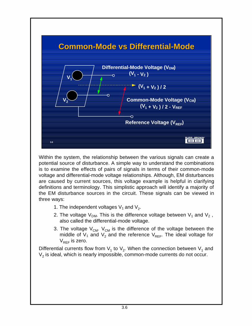
Within the system, the relationship between the various signals can create a potential source of disturbance. A simple way to understand the combinations is to examine the effects of pairs of signals in terms of their common-mode voltage and differential-mode voltage relationships. Although, EM disturbances are caused by current sources, this voltage example is helpful in clarifying definitions and terminology. This simplistic approach will identify a majority of the EM disturbance sources in the circuit. These signals can be viewed in three ways:
1. The independent voltages V1 and V2.
2. The voltage VDM. This is the difference voltage between V1 and V2 , also called the differential-mode voltage.
3. The voltage VCM. VCM is the difference of the voltage between the middle of V1 and V2 and the reference VREF. The ideal voltage for VREF is zero.
Differential currents flow from V1 to V2. When the connection between V1 and V2 is ideal, which is nearly impossible, common-mode currents do not occur.
3.6
Differential-Mode Voltage (VDM)(V1 - V2 )
Common-Mode vs Differential-ModeCommon-Mode vs Differential-Mode
V1
V2
Reference Voltage (VREF)
(V1 + V2 ) / 2
Common-Mode Voltage (VCM)(V1 + V2 ) / 2 - VREF

3.7
The radiation from a circuit can come from two different relationships between two or more current sources, common-mode radiation currents and differential-mode currents. The differential-mode radiation currents in a circuit are a natural consequence of the physical layout. They occur as a result of separate PCB traces with differing current densities. The resulting phenomena from these currents is a differential-mode H-field radiation.
Likewise, common-mode radiated currents are created as a result of losses due to cables and traces of the printed circuit boards. Common-mode currents create radiated signals that are predominately E-fields.
3.7
Current Coupling PathsCurrent Coupling Paths
Emission
Differential-ModeRadiation
Common-ModeRadiation
ANTENNA

3.8
Common-mode radiated signals can be measured during the design phase to determine if corrective action should be taken, such as a change in the PCB layout or system configuration. The emission of the most devices is dependent on the magnitude of the high frequency currents on cables and traces.
A guideline commonly used for maximum allowed common-mode current is ICM<5µA (assuming r = 3 meters). Conversely, the general rule of thumb used for the emission measurements of radiation is a maximum of 30µV/m.
The relationship between common-mode current and the radiated electrical field is:
E = 60 ICM / r
where,
E = Electrical field strength (V/m)
ICM = Common mode current (A)
r = Distance from common-mode current source (m)
Common-mode currents that couple signals into the environment can be measured with the set-up shown above. These emissions can be due to parasitic capacitive coupling between lines or from a line to the earth ground. For differential measurements the same equipment can be used by turning one wire one time around the transformer.
3.8
Measurement of CM CurrentMeasurement of CM Current
Electric-field limit is 100µV at a distance of 3 metersCommon-mode current maximum is 5µA
I1
I2
ICM = I1 - I2 LOADSOURCE
Transformer
SCOPE
ICM

3.9
Common-mode current signals can cause unwanted radiation. The radiation can be reduced by placing a choke or clamp in the path of the current. The low pass filter or choke is easy to implement. The low pass filter can be designed using an RC combination. If this approach is not feasible, the choke can be constructed by winding wire a few turns around a ferrite core or bead. The choke will act to restrict high frequency dI/dt signals through the conductor. As the frequency in the line increases so does the influence of the choke. Digital ribbon cables can also present a problem in terms of radiated signal due to common-mode currents. When a ferrite bead is not feasible a ferrite clamp can be used instead. It is important to note that differential-mode currents are not affected by this technique of radiated noise reduction.
3.9
Reducing CM-CurrentsReducing CM-Currents
Use ferrite beads or clamps to reject the common mode currents

3.10
The magnetic H-field strength is inversely proportional to the distance from the source. The relationship between the magnetic field, H, and the far electric field, E, can be calculated as shown below with the following assumptions:
Distance from the H-field = 0.1m
Distance from the E-field = 3m
(legal cable length for consumer products)
For frequencies below 16 to 300MHz
An antenna or probe can be built with a coax cable and used to measure the magnetic field. The H-field induces a voltage signal across the 50Ω resistor. This voltage increases with lower frequencies. For a frequency above 300MHz the sensitivity of the probe becomes independent of the frequency. At that point the voltage will increase with the frequency but the current does not increase because 2πf L is larger than 100Ω (where L is the inductance of the probe). This resistor value is the sensor impedance added to the input impedance of the measurement system. Once the H-field has been measured with this technique, the E-field can be estimated by the following formula:
With : E = electrical field strength (V/m)
H = magnetic field strength (A/m)
f = frequency (Hz)
3.10
Measurement of Magnetic FieldMeasurement of Magnetic Field
Measure the field with the “coax” probe
0.1m
PROBE
Use a coax cableto make probe
Remove coaxshield
50Ω chipresistor
To 50Ωmeasuring system
30 mm
E(r=3m) ≈ 2.7 • 10 • f • H (r=0.1m)

3.11
Electromagnetic interference that occurs in an application can be explained by the previous discussion or it may have unexpected behavior. Many times a possible explanation for this unexpected behavior can be attributed to the components in the circuit. If the components operate at higher frequencies, they are usually the primary contributors to the unexplainable high frequency disturbances. These high frequency disturbances are magnified by the PCB and component parasitic inductances and capacitances. Keep in mind that passive components have a parasitic characteristics as well.
The next slides give some more information about the parasitic properties of passive components and after some suggestions on how to reduce the EMI-dependence of the circuit.
3.11
The EMI-propertiesThe EMI-properties
• Application will sometimes produce results normally not expected
• These problems usually occur at frequencies higher than bandwidth of active components
• Keep in your mind :
Parasitic Effects

3.12
Whenever current flows through a conductor, an EM-field is created. Consequently, EMC troubleshooting always starts and ends with the evaluation and relationships of currents in the circuit. It is possible to have a current flowing in a circuit without a supply voltage. An example of such an occurrence is a magnetic field which generates a current in a toriod. Regardless of whether or not a voltage source is present, Kirchhoff’s laws can still be applied to a circuit throughout the EMC evaluation. As stated by Kirchhoff, the summation of the currents at any node in a circuit is always zero.
When emissions occur in a device, the radiated energy path is modeled as one of the current vectors that intersect the circuit node under analysis. In the case of the diagram above, I2 represents a radiated signal. Additionally, current can be “injected” into a circuit as shown above. This type of circuit is said to be susceptible to EMI.
3.12
Work with Currents!Work with Currents!to meet EMC-specificationsto meet EMC-specifications
• There can be a current without a voltage-source
• Every current creates an electromagnetic field
• Currents are sensitive to emission and susceptibility
• With EMC, current dominates the evaluation!!
Emissions
I1
I2
I3
Susceptibility
I

3.13
The equivalent circuit of a resistor or PCB trace also has inductance and capacitance in the model. Parallel circuits can be used to minimize the influence of the parasitic components at high frequencies. Concurrently, it is recommended to shorten leads as much as possible to minimize the inductive contribution of the PCB implementation.
Normally capacitors are selected for their characteristics over a specific frequency range. For that frequency range the capacitor acts like a short circuit. They are particularly useful between the power supply rails and ground, in which case they filter supply noise that the circuit components are incapable of rejecting. The same technique can be applied to an EMC problem, where a short circuit caused by a capacitor occurs at the specific frequency where the EMC problem is occurring.
Capacitors operate like short circuits in the higher frequencies, conversely inductors operate like open circuits. Normally an inductor has a core in order to obtain a relatively high induction for a relatively small coil size. The behavior of the coil and core vary over a wide frequency range. The coil will resonate at a specific frequency because of the capacitance from wire-to-wire and wire-to-metal housing can. Below this resonant frequency, the coil will behave like an inductor. Above this frequency it appears to be capacitive.
3.13
Passive ComponentsPassive Components
• Parasitic components of a circuit are reduced with a parallel circuit
• Capacitors should be a short at the frequency of the EMI-problem
• Coils have many parasitic components: check for resonance
3.14
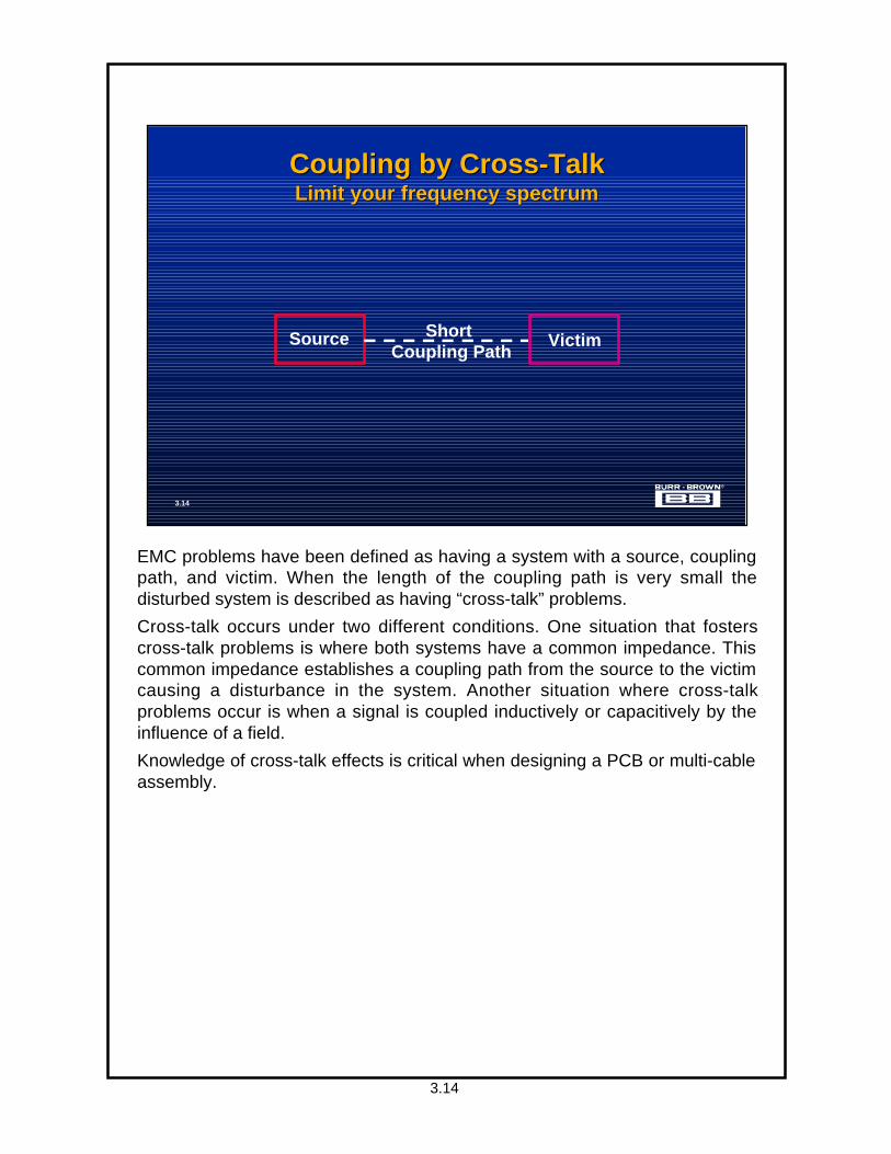
EMC problems have been defined as having a system with a source, coupling path, and victim. When the length of the coupling path is very small the disturbed system is described as having “cross-talk” problems.
Cross-talk occurs under two different conditions. One situation that fosters cross-talk problems is where both systems have a common impedance. This common impedance establishes a coupling path from the source to the victim causing a disturbance in the system. Another situation where cross-talk problems occur is when a signal is coupled inductively or capacitively by the influence of a field.
Knowledge of cross-talk effects is critical when designing a PCB or multi-cable assembly.
3.14
Coupling by Cross-TalkCoupling by Cross-TalkLimit your frequency spectrumLimit your frequency spectrum
Short Coupling Path
Source Victim

3.15
It is not uncommon for a common conductor to cause cross-talk between two systems. As shown in the diagram above, the currents of two separate circuits flow through one conductor, ZK, to a common reference, which is usually ground. In order to minimize the effects of the changes in voltage across ZK, the impedance ZK should be low. An evaluation of the signal to distortion ratio of this circuit is an easy way to start to understand the affects of cross-talk with this simple circuit. Intuitively it is easy to see that the signal-source VS1 will contribute to the ultimate voltage drop across the impedance ZL2 and VS2 will do the same to the voltage drop across ZL1 if the impedance of the common conductor, ZK, is not equal to zero.
To look at the contribution of VS1 to the voltage drop across ZL2 the assumptions are that VS2=0 and ZK<< other impedances in the circuit. The results of the final calculation is:
Cross-talk is dependent on the impedance of the common conductor, ZK. When ZK is zero the cross-talk is zero. The effect of the cross-talk to the signal to distortion ratio is :
A calculated S/D ratio is shown below :
ZS1=10Ω, ZL1=50Ω, ZK=0.1Ω and VS2 / VS1=0.01
---->> S/D = 15.5 dB
3.15
Cross-talk by Common ImpedanceCross-talk by Common Impedance
Signal / Distortion dependence of ZK
ZS1
VS1 VS2
ZS2
ZL1
ZK
ZL2
+ +1
2
I1 I2
VZL2 / VS1 = ZK ZL2 / [ (ZS1 + ZL1 )(ZS2 + ZL2 )]
S / D = VZL2 WITH ZK = 0 / V ZL2 WITH SMALL ZK = [(ZS1 + ZL1) VS2 ] / (ZK VS1 )

3.16
In order to reduce the effects of ZK some options can be exercised. The common line between the two circuits can be eliminated by using a second common line as described in the circuit above. This may not be feasible and a second option would be to attempt to keep the impedance, ZK, as low as possible. This can be accomplished by shortening the lead length from node 1 to node 2 or dedicating one layer of the PCB to achieve a low impedance reference path. A final solution that can be implemented is to keep the current between the circuits low with a galvanic separator such as an isolation amplifier or optocoupler, for example.
3.16
Reducing Common Impedance Reducing Common Impedance
• Use two conductors instead of one
• Keep the common impedance ZK low
• Keep the current through ZK low
VS1
I2+
+ I2
ZS1
ZS2
VS2
ZL1
ZL2

3.17
An isolated instrumentation amplifier is used here to galvanically separate a bridge circuit. The input to the ISO213 is a high impedance differential input with adjustable gains. Included in the package is a DC/DC converter that is used to power the isolated (input) side of the isolation instrumentation amplifier and external circuitry, such as the REF1004C and OPA130.
For any isolation product, the barrier integrity is of paramount importance in achieving high reliability. The ISO213 uses miniature toroidal transformers designed to give maximum isolation performance when encapsulated with a high dielectric-strength material. The internal component layout is designed so that the circuitry associated with each side of the barrier is positioned at opposite ends of the package. Areas where high electric fields can exist are positioned in the center of the package. The result is that the dielectric strength of the barrier typically exceeds 3kVrms.
The reference circuit, REF1004C (+2.5V) provides voltage power for the bridge. The low power, FET input OPA130 drives the bottom of the bridge, providing a linearity correction of the single element bridge.
3.17
Isolated Instrumentation AmplifierIsolated Instrumentation Amplifier+VSS
-VSS
+2.5VREF1004C
+VSS 1kΩ 1kΩ
1kΩ1kΩ
+
-
OPA130
+
-
-2.5V
-VSS+VSS
VOUT
+15V
RS
ISO213

3.18
In the first figure, an op amp is connected in a standard non-inverting gain configuration. Three sources of error are shown: (1) External resistors RF and RIN are meant to set the gain, but the input signal, VSIGNAL, is amplified by 1+RF/(RIN+RGND) instead of 1+RF/RIN, (2) VNOISE represents noise pickup in the signal path, (3) VERROR represents ground loop errors due to ground currents from other circuitry reacting with wiring impedance, RGND. With an op amp, the effects of all error sources appear at the amplifier output, with gain applied.
When a classical instrumentation amplifier is used, noise (VNOISE) and other errors (VERROR) are rejected. The second figure shows an instrumentation amplifier connected with the same error sources shown previously. A classical instrumentation amplifier is comprised of two stages. The first stage uses two amplifiers which provide a high impedance, differential input gain stage. The second stage is configured as a unity gain differential amplifier with four resistors, changing the differential output of the first stage to a single output signal. Gain of the instrumentation amplifier is set by a single-ended external resistor, RG. The gain equation depends on feedback resistors contained in the instrumentation amplifier and RG. With 25kΩ internal feedback resistors, the input signal, VSIGNAL is amplified by 1+50kΩ / RG.
3.18
IAs Reject Noise and ErrorsIAs Reject Noise and Errors
+
-
V NOISE
V SIGNAL V O
R F
I GND
R GND
V ERROR
R IN
V OUT
G = 1 + 50kΩ/(R IN + R GND)V OUT = G(V SIGNAL + V NOISE) + (G - 1)V ERROR
50kΩ
+
-
V NOISE
V SIGNAL V O R G
I GND
R GND
V ERROR
V REF
V OUT
G = 1 + 50kΩ/RG
VOUT = G (VSIGNAL)

3.19
Cross-talk between two circuits can occur when there is a common conductor between the systems. The coupling path medium supports current and voltage changes directly. Other problems can arise from EM-fields as well. As discussed previously, currents cause electric or magnetic fields. These “air born” EM-fields can couple into other circuits within certain distances. This type of cross-talk can be separated into two categories, capacitive and inductive cross-talk.
Capacitive coupled cross-talk disturbances are transmitted electric fields. In the diagram we can see the measuring set-up of two parallel circuits with the equivalent circuit shown below. The capacitive coupling occurs through the capacitor CAB. If the value of the capacitance of CAB is decreased, the cross-talk problem is also decreased.
Using the equivalent circuit the following formula is derived:
From this formula the following conclusions about cross-talk can be found:- Capacitive coupling acts like a High pass filter - Cross-talk increases with increasing ZL.
- Cross-talk is dependent on the ratio of the voltages.- The cross-talk signals are in phase with each-other.
3.19
Capacitive Cross-TalkCapacitive Cross-TalkCoupling by electric fieldsCoupling by electric fields
• Coupling looks like high pass filter
• Cross-talk increases with increasing Z
• Voltages responsible for coupling
• Signals are in phase
ZL1
ZL2
CAB
CircuitB
CircuitA
ZL1 ZL2
CircuitB
CircuitA
CAB
VSOURCE
ZL
VLOAD / VSOURCE = 0.25 jωZLCAB

3.20
Traces on the PCB form parasitic capacitors with other traces. The magnitude of the capacitance is dependent on the ratio of the length of the two traces and the distance between them. This first order calculation gives the designer a rough estimate of the stray capacitance that has been designed into the PCB layout.
3.20
PCB CapacitancePCB Capacitance
w Ldeo
er
= width or thickness of PCB trace= length of PCB trace= distance between the two PCB traces= dielectric constant of air = 8.85 X 10⁻¹² F/m= dielectric constant of substrate coating relative to air
w • L • eo • erC = pF
d
w(typ 0.003mm)
PCB Trace
dL
PCBCross-Section

3.21
Cross-talk can conduct between traces and layers on the print circuit board, but contacts of switches and relay pins of connectors or leads of components can also be a source or victim of cross-talk.
In order to decrease the capacitive cross-talk, the capacitor value of CAB should be decreased. The value of the capacitance will decrease with decreasing the surface area or increasing the distance between the two conductors. When it is impossible to change one of these two variables, the capacitor value can be changed by mounting shields around one of the two conductors.
3.21
Reducing Capacitive Cross-TalkReducing Capacitive Cross-Talk
• Decrease the adjacent surfaces• Increase the distance between two circuits• Create a guard between the two circuits
ZL1
CircuitB
CircuitA
Shield

3.22
This slide models the basic electric field coupling affect with an inverting op amp configuration, an electric field noise source (eE), and the mutual capacitance (CM). The source eE couples a noise current INE through CM and into the amplifiers feedback network. That current flows through the feedback resistor, R2, to produce an output noise signal -(INE R2). In practice, other mutual capacitances couple noise currents to other points in the circuit, however, the low impedance at these other points minimize the effects of the currents.
Switching to a differential input configuration produces balanced conditions that allow the op amp’s CMR to reject the noise signal - (INE R2).
3.22
Electrostatic CouplingElectrostatic Coupling
R2eOUT = – eIN – (eE • R2 • CM(s))R1
INE = eECM(s)
+
-ElectrostaticCoupling
eE
CM INE
OPA131
eOUT
eIN
R11kΩ
R210kΩ

3.23
This circuit operation uses a simple method of noise reduction. Adding balancing resistance in series with the op amp’s non-inverting inputs cancels noise coupled to those inputs. Further examination reveals the impedance balance that the technique produces. From the figure, the impedance that drives from the op amp's inverting input also equals R1 || R2. R1 returns to the low impedance of a source, and R2 returns to the low impedance of the amplifier’s output. Thus, for impedance analysis purposes, these two resistors effectively return to ground and appear in parallel. Therefore, the op amp’s CMR rejects the electric field coupling as long as the circuit presents equal impedances to the two op amp inputs.
The RB resistors resemble those often added to reduce the DC offset produced by amplifier input currents. These resistors will cancel coupled noise and offsets caused by input currents, however, this does not preclude bypassing with capacitors across R2. Bypassing would again cause an imbalance in the impedances that drive the amplifier inputs over frequency.
3.23
Using CMR to Reduce Electrostatic Using CMR to Reduce Electrostatic CouplingCoupling
+
-ElectrostaticCoupling
eE
CM
OPA131
eOUT = eIN
eIN
R11kΩ
R210kΩ
RB = R1 R2
–R2
R1

3.24
Magnetic-coupling dominates inductive cross-talk. This kind of coupling can be compared to a transformer. In the circuit above a factor, M (mutual inductance), is given for the inductive coupling by the two coils.
For the equivalent circuit the formula below can be derived:
From this formula the following conclusions about cross-talk can be found:
- The coupling has a high pass filter characteristic. This is the same as in the capacitive coupling case
- With the same couple factor, M, the cross-talk will increase by decreasing ZLOAD
- Changes in current are responsible for cross-talk
- The undesirable voltages are out of phase
3.24
Inductive Cross-TalkInductive Cross-TalkCoupling by magnetic fieldsCoupling by magnetic fields
• Coupling looks like high pass filter
• Cross-talk increases with decreasing Z
• Changes in current are responsible for the coupling
• Signals are out of phase
ZL
M
VLOAD / VSOURCE = - 0.25 jωM / ZL

3.25
The techniques that are used to reduce inductive cross-talk are similar to the methods used for capacitive cross-talk reduction. The coupling factor between the inductors should be reduced as much as possible. This can be achieved by increasing the distance between circuits, causing the field to reduce with the inverse of the square of the distance. Another approach would be to twist the wires of the two circuits.
The relationship of the distance between two current conducting circuits and the strength of the magnetic field can be first order approximated with the following calculations. In this example, the magnetic field at point X generated by the wires of Circuit A with a current magnitude is calculated :
H ≅ IA / 2 π • D1 / RX2
This equation mathematically illustrates that the magnetic field strength is inversely proportional to the squared distance between the two circuits.
A second approach to reducing the coupling factor is to twist the wires of the two different circuits. The H-fields will counteract each other, reducing the cross-talk effect.
3.25
Decrease Inductive Cross-TalkDecrease Inductive Cross-Talk
• Increase the distance (RX) between two circuits• Twist the wires of the two circuits to counteract
their fields
RXD1
Circuit A Circuit B
I
IX Twisting Reduces the
H-Field as Well

3.26
For op amp circuits, the most confusing task in inductive coupling reduction can be identifying the pick-up loops. The physical arrangement of the circuit’s components form these loops in several ways. The circuit above shows the loops in a non-inverting op amp circuit. The op amp connections with the source, the feedback and the load form three loops. The op amp seems to break these loops, but the amplifier’s feedback action continues them.
First, the ground return of resistor R1 forms loop L1 with coupled noise source eM1. This loop’s noise signal eM1, drives an inverting amplifier that provides gain of -R2/R1. This gain potentially makes the loop, L1, a serious noise source and a good choice for area minimization.
Next, consider loop L3 and its coupled signal eM3. This less obvious loop exists because e1 and RL connect at the circuit’s ground return, and feedback extends the signal path through the amplifier. Signal e1 drives the input of the non-inverting amplifier. Feedback makes the amplifier output respond to e1, continuing the loop between the top of e1 and RL. The resulting noise signal, eM3, appears at the load with unity gain.
The final loop, L2, depends on the loop continuity conditions described for L1 and L3. The resulting noise signal eM2, also appears at the circuit output with unity gain.
3.26
Magnetic Coupling and Op AmpsMagnetic Coupling and Op Amps
R2
L1
L2
L3
OPA131eO
+ -
+
-
- +
eI
R210kΩ
RL1kΩ
+
-
eM3
eM2
eM1
R11kΩ
eO = 1 + • e1 - • eM1 - eM2 + eM3R1
R2
R1

3.27
Minimizing the preceding loops reduces the magnetically coupled noise, but does not eliminate it. Some finite loop areas and magnetic coupling always remain. However, the difference amplifier's CMR reduces the noise further. The circuit above shows the relevant loops and coupled noise signals for this amplifier. The ground of the differential input acts as a center tap for L1 pick-up loop, splitting the eM1 signal into two equal parts. Unfortunately, these parts present opposite polarity signals to the differential input’s, R1, resistors. Now, instead of a common mode input, the net eM1 presents a differential signal, which the circuit’s CMR does not reject.
However, the balanced structure of the difference amplifier still permits noise reduction by matching loops L2 and L3. These loops produce the signals eM2 and eM3, which tend to cancel at the circuit output.This cancellation requires matching the loops of L2 and L3, their distances from any interfering magnetic source, and their orientations relative to that source. Matching these three features equalizes eM2 and eM3, making their net effect a common mode signal at the amplifier’s inputs. Matching loop areas and distances equalizes the magnitude of eM 2 and eM3. Matching distances produces first order phase equalization. Accurate phase matching, which high common mode cancellation requires, also necessitates matched loop orientations relative to the magnetic source. Most often, this noise reduction technique aids in the rejection of low frequency noise, such as power transformer interference.
3.27
Difference Amplifier Reduces Noise FurtherDifference Amplifier Reduces Noise Further
R2eO = (e2 - e1) - eM1 + (eM3 - eM2)R1
R2
R1
L1
L2
L3
OPA131eO
+ -+
-
- +
eI
R210kΩ
RL1kΩ
+
-
eM3
eM2
1/2 eM1
R11kΩ
R210kΩ
R11kΩ
+1/2 eM1
-
e2
+
-
+
-

3.28
To further the precision of the difference amplifier, a monolithic version is available. Because the monolithic difference amplifier has thin film resistors on the chip, the loop areas are reduced to a minimum. Additionally, the resistors are trimmed precisely to obtain better than average CMR.
3.28
Monolithic Difference AmplifierMonolithic Difference Amplifier
+
-
20V max RS
I
+VIN
-VIN
-VREFINA105
25kΩ25kΩ
25kΩ 25kΩ
VOUT = I • RS
Loadfor
Supply
Feedback
VOS
VOS/TVCM
Gain ErrNonlinearity
= 1000µV (max)= 20µV/°C (max)= ± 20V= 0.01% (max)= 0.001% (max)

3.29
These points summarize the discussion on performance improvements when cross-talk is a problem.
3.29
Cross-Talk ReductionCross-Talk Reduction
• Each Circuit should have its own conductors
• Keep conductors in circuit as close as possible to reduce loop area
• Place a small resistor in the signal and/or supply lines
• Use only the bandwidth that is NEEDED
• For PCB designs use double or multi-layers to create conductive shields

3.30
Ground is a concept that is used by most engineers in their daily work. Grounding a circuit can sometimes be taken for granted and later on in the proto-typing process present some of the most bewildering problems. Many EM-problems can be attributed to a poorly grounded circuit.
In EMC-applications the ground or earth-protection is often referred to as the system reference (SR). The system reference defines a central point in a circuit that is used to check other signals.
The SR is often defined at the supply which is usually connected to earth ground. Keep in mind, the SR is a connection that will probably have many incoming and outflowing currents.
The determination of the location of the system reference is very important. The impedance of the SR should be as low as possible and EMI signals in the area kept to a minimum. To meet these requirements, EMC knowledge should be applied when designing the layout.
The determination of the location of the SR is dependent on:- Circuit emissions
- Circuit immunity- Circuit conductors
- Placement of the components
3.30
Earth and ReferenceEarth and Reference
• Create in your application a System Reference (SR)
• The SR must be LOW IMPEDANCE• Placement of the SR is dependent on
– emission– immunity– conductors– position of components

3.31
The effects of a bad reference (SR) in an EMC-application problem is illustrated here. In this example, a dual, single supply op amp, OPA2234, is configured as a two op amp gain stage. The SR is represented by the symbol . The layout was designed without EMC-considerations taken into account. The results, in terms of a signal-distortion ratio are summarized in the following formula:
S/D = VIN / ( I1ZA ) + ( I2 + I4 )(ZA + ZB) - ( I3 ZC )
where ZA, ZB and ZC are trace impedances.
The system reference in this layout is not ideal, causing EMI errors. In order to reduce cross-talk, the layout should eliminate the currents that flow through the SR. The currents are :
I1 = current through the smoothing capacitor
I2 = amplifier ground current
I3 = aerial current of the input cable
I4 = load current ZL
One approach to eliminating this problem is to make the impedance of the system reference as low as possible. This can be achieved by using a ground plane, grid or strip.
3.31
Effects of a Bad ReferenceEffects of a Bad Reference
S/D = VIN / (I1ZA) + (I2+ I4)(ZA+ ZB) - (I3ZC)
I1
I3Input
ZLOAD
I2
I4ZC
ZB
ZA
+
-
OPA2234+
-
System ReferenceAC
OPA2234
+
-
12
3
6
5
7 1
I4 +
-

3.32
An improved layout reduces the EMI risk. The signal reference is changed from a PCB trace to a strip, making the SR low impedance. This lowered impedance essentially eliminates the impedances ZA, ZB and ZC thereby improving the cross-talk error. The SR layer also makes it possible to place passive low pass filters on the input and output of the amplifiers to further reject out of the band noise.
3.32
Layout with low impedance SRLayout with low impedance SR
Input Output
+
-
OPA2234
AC

3.33
When multiple boards are in the system, a “star” configuration is recommended as a the better configuration for supplies and system references. This technique allows for a lower impedance system reference and eliminates the larger differential current loops (ground loops). Short cables connected to one side of each board gives the best performance. Lack of planning can create difficult loop problems down the road. A typical example is shown above of how not to configure a system. This circuit is prone to produce differences in the potentials of the individual board system references.
3.33
Connecting More Than One PCBConnecting More Than One PCB
THE RIGHT WAY THE WRONG WAY
PCB1 PCB2
PCB4PCB3
PCB1 PCB2
PCB4PCB3
Connector
MAINS
MAINS

3.34
Many times circuit designs contain a variety of high speed vs low frequency components and analog vs digital components. Generally, the best performance is achieve if these groupings of components are kept in close proximity. For example, the analog devices are positioned to reside on the same ground plane and the high frequency components are grouped separately from the medium speed and low frequency components. Additionally, the high frequency circuits should be placed close to the connectors. This will shorten the length of the interconnects, consequently reduce line inductances.
Another good layout technique would be to separate the ground planes of the digital and analog sections. This technique could reduce a considerable amount of cross-talk between the two types of components. These general guidelines offer the designer a starting point in the PCB layout. There are, of course exceptions to these suggestions, such as the grounding practices with a A/D converter. In the case of an A/D converter, both the analog and digital ground connections should be connected to the analog ground plane.
3.34
Component PlacementComponent Placement
High Frequency Componentsplaced near the connectors
Separate Digital and AnalogSections of the Circuit
high
low
freq
uen
cy
Dig
ital
Analog
A/D
Bu
ffer
Dig
ital

3.35
As previously discussed, the connectors of the PCB should be as close to the high speed section of the circuit as possible. Shorter traces make the layout less sensitive to the high frequency interference that happens to be in the signal bandwidth.
The two traces above are used to illustrate the implications of these statements. The first trace has a length of 0.06m making a perfect antenna for frequencies that are multiples of 5GHz. The trace length can be changed as shown with the second trace. In this illustration, the longest trace length is 0.018m making that trace sensitive to frequencies that are multiples of 16.6GHz.
3.35
Decreasing the Antenna EffectDecreasing the Antenna Effect
Trace 1 : f 1 = c / L = 5.0 GHz
Trace 2 : f 2 = c / L = 16.6 GHz
0.06m
c = 3 x 10⁸ m/s, L = length of the trace
0.018m
All cornersshould have45 ° angles

3.36
Cables and connectors in applications require special attention because they can act like antenna for transmission and receiving.
The most important parameter of a cable is the transfer impedance ZT. ZT, also known as cable impedance, is the coupling mechanism used to send signals from circuit to circuit. The transfer impedance as well as the leakage characteristics of a cable provide a mechanism for susceptibility and emission in the EM-environment.
Many engineers assume that a coax cable is sufficiently shielded for EMC-applications. This may not always be the case because the coax cable can have higher leakage than expected. This is due to the fact that the coax shield consists of only one conductor. Higher quality coax cables have lower leakage and lower line impedance, ZT. Once a cable with low ZT is selected, the quality of the connections between cable and board can have a great influence on the EM leakage issue.
Glass fiber can be a good alternative to coax cables. It is true that the actual fiber is immune to EM interference, however, be aware that the electronics on both sides (usually high speed) must be EM compatible.
3.36
Cables and ConnectorsCables and Connectors
• Cables are perfect antenna for emissions and susceptibility
• ZT is the coupling between desirable signal circuit and the (undesirable) common-mode signal
• The transfer impedance ZT gives the leakage of the cable

3.37
In this application, the cable connection between the Instrumentation amplifier (INA118) and the load is sensitive to emitted signals. These unwanted signals will be added to the common-mode signal and appear on the load. Before a quantitative answer can be determined concerning the magnitude of the interfering signal, the inductance of the wires in relation to the interfering signal require evaluation.
3.37
Influences of the CablesInfluences of the CablesThe transfer-impedance of the cableThe transfer-impedance of the cable
VCM will add an undesirable signal.
The cable impedance is dependent for the value of this signal.
+
-
75kΩ
75kΩ1µF
+15V
-15V
A B
C DRL
VCM
Source Cable Load
INA118

3.38
The equivalent circuit for the INA-application is shown in this circuit. The cable’s inside and outside impedance is used to explain the influence of the connection between source and load. The impedance, Z, serves as the coupling path for the undesirable signal VCM and the coupling factor, M, facilitates the inductive cross-talk. The total effects of EM coupling is shown below:
With L and M = Source + Cable + Load.
Since the cable specifications are of most interest in this example, they are separated from the other circuit coupling paths. The total impedance of the cable called the global transfer impedance (ZTG), can be used in this calculation. The global transfer impedance describes the entire connection. To obtain the global transfer impedance of a particular system, the transfer impedance is multiplied by the total length of the specific system. ZTG gives a value for leakage, derived from a combination of resistive, capacitive and inductive factors. A low value of ZTG is equal to a low leakage of the cable resulting in a low common voltage.
With LC, RC and MC = Cable
This approximation is only applicable to low frequency applications where L <= λ / 10, where L=length (m) and λ=wave length (m).
3.38
The Global Transfer-ImpedanceThe Global Transfer-Impedance
ZTG = L ZT = RC + jω ( LC - MC )( L < = λ / 10 )
SOURCE LOADM
VCM RC
RB
RA LA
LB
ZTG = ZCABLE = RC + jw (LC - MC )
ZT = RB + jw ( LB - M )

3.39
Once the EM-leakage is determined using the global cable impedance, the cable connections should be evaluated. The addition of the contribution of EM-leakage by these connections complete the EMI picture. The total impedance ZTV is calculated below:
ZTG = global cable impedance
ZTCS = connection source impedance
ZTCL = connection load impedance
When a circuit is low impedance a good connection can be made and disturbance signals are also low. A low impedance connection can also be made by steering the disturbance current to the cover of the device.
The best and not so good approaches to configuring grounds in a connector are shown in the diagram above.
3.39
The Total EM-LeakageThe Total EM-Leakage
Choosing the rightpin configuration
Low impedancebetween cable and cover
BEST
WORST
SR
Signal
I
Low Z
ZTV = ZTG + ZTCS + ZTCL

3.40
Multi-cable assemblies are unavoidable in big applications. For the cables inside a machine or other kind of device, the kind of signals that they are carrying, dictate proper groupings of the cables. If these guidelines are used, cross-talk and disturbances problems can be reduced.
- Do not combine the wires with inductive loads such as relays or motors together with digital cables.
- When a mains filter is used, do not add the primary and secondary wires of the filter in the same multi-cable assembly.
- High-frequency signal cables may not be in the same multi-cable assembly as the cables transmitting sensor signals.
- Do not lay the wire of the earth protection in a multi-cable assembly. The other cables can be disturbed by the earth-wire causing common-mode problems.
3.40
How to make Multi-cable AssemblyHow to make Multi-cable Assembly
• Separate signal and power cables• Separate primary and secondary of the
mains filter wires• Separate Sensor cables from power and
digital cables• Earth ground should have its own housing

3.41
When a design is constructed using EMC guide-lines it is possible that the EMI is still to high. Further action can be taken to reduce these signals with shielding (Faraday shielding) around the housing. Shielding will help to reject emission and improve immunity.
In the most cases the metal housing of the device will work as a shield. In the case where the housing is made of plastic it is possible to paint the inside of the housing with a conductive coating or place a conductive foil against the cover.
Most covers need holes for wires or cooling lines. When the device needs these holes in the housing many smaller holes are better than one big hole. The wave length of the unwanted signals that come through the holes is determined by the formula: λ = c / f.When selecting shielding material RFI and magnetic coupling are dealt with separately. The frequency differences of the two interference sources necessitate the use of different shielding materials. At lower frequencies, only ferromagnetic materials offer the properties needed for shields at a practical thickness. At higher frequencies, decreases in both the shield thickness requirement and the magnetic response of ferromagnetic materials make copper a good alternative. Even the copper layer of a ground plane becomes an effective magnetic shield.
3.41
Shielding your applicationShielding your application
• Use a low impedance cover
• Make good connections between different parts of cover
• Make many smaller holes instead one big
• Use conductive foil with a plastic cover
Use smaller holes
No PaintLow Z
λ = wave length (m)c = speed of light (m/s)f = frequency (Hz)

3.42
It is important to know what kind of interference signals need damping. If the signal’s source creates an electric-field it may require different shielding strategies than if the signal source creates a magnetic-field.
The E- and H-fields have different impedances. The impedance of an E-dipole, ZE, has a higher impedance in air than the H-dipole, ZH. In the near-field the high impedance in air of the E-field and the low impedance of the H-field is:
For E-fields the damping factor is : SE = 2 σ d / 3 ω ε0 rE-field :
- Damping decreases with increasing frequency
- Damping decreases with increasing of distance between source and shield.
For H-fields the damping factor is : SH = ω υ0 r σ d / 3
H-field:
- Damping increases with increasing field
- Damping increases with increasing distance between source and shield.
(ε = dielectric constant, υ = permiability, r = distance from the source to the sheild)
3.42
Shielding Attenuates EMIShielding Attenuates EMI
• The effect of an E-field :– Damping decreases with increasing frequency– Damping decreases with increasing distance
between source and shield• The effect of an H-field :
– Damping increases with increasing frequency– Damping increases with increasing distance
between source and shield
ZE = 1 / 2 π ε f rZH = 2 π υ f r

3.43
Shielding a device can have positive results as well as negative. Parasitic capacitance between the shield and the circuit is a natural consequence. These capacitances, if large enough can create a large enough feedback path to a critical node in the application. The most simple direct solution to this type of problem is to connect the shield to the low impedance of the system reference.
3.43
Connect Shield to ReferenceConnect Shield to ReferenceSHIELD
SR
SHIELD
Connect Shieldto System Reference
SR

3.44
As a last resort, a mains filter should be employed. A mains filter rejects small emissions noise and enhances the immunity. A mains filter can be constructed mechanically, using shielding techniques or electrically using capacitive by-pass techniques or RC filters. This filter is not necessarily enough to meet EMC requirements alone. The design should be carefully configured according to the EMC guidelines and then a filter may help reach the required performance.
Mains filters can be used with the following guidelines:
1. Be sure there is good connection between the reference of the filter and the protecting earth ground by keeping the connection as short as possible.
2. Reject capacitive and inductive cross-talk between the input and output of the filter.
3. When mounting the metal filter cover to the application, be sure there is a good contact. Mounting on painted metal or anodized aluminum can give problems.
4. Keep the cables from the secondary filter side to the circuit as short as possible.
5. Don’t bring the cables to and from the filter together in one cable bundle.
When it is not possible to avoid a coupling between the circuit or PCB(s) and the filter input or output cables, a shield can be inserted between filter network and the PCB cables.
3.44
Using a Mains filterUsing a Mains filter
• Keep connection filter/protecting-earth as short as possible.
• Reject cross-talk between in- and output.
• Keep cables as short as possible.
• Don’t bring input and output cables together.
Filter
Equipment
The ideal position for the filter

3.45
Often an isolation device such as an isolation amplifier or opto-coupler is used for galvanic separation and/or reduction of common-mode voltages. With these devices, a light source, magnetic field or electric field is used to transmit the circuit signal in order to obtain the galvanic separation. There is a parasitic capacitance between the input of the devices to the output. The equivalent circuit shows the parasitic capacitance of an isolated instrumentation amplifier, ISO175.
The ISO175 is also an isolation instrumentation amplifier, similar to the ISO213, except the ISO175 does not have an on-board DC/DC converter. Additionally, the isolation is achieved with E-field transmission across the barrier through embedded capacitors in the package.
It is not unreasonable to expect emissions of 1GHz in an EM-environment. When the effects of the isolation amplifier’s parasitic capacitance is evaluated at that frequency it operates like a low impedance resistor. For example :
f = 1 GHz
CISO = 2pF (for the ISO175)
Similar total values of isolation capacitance can be found in circuits using opto-couplers, where the signal and communication paths use a total of 3 or 4 opto-couplers. In this case, the total is equal to the summation of the isolation capacitance of the individual couplers.
3.45
The rejection of CM-signalsThe rejection of CM-signals
• Galvanic isolation will reject CM-signals
• All galvanically isolation devices have parasitic capacitances
• CISO : 0.4pF to 10pF
CISO
SIGNALINPUT
SIGNALOUTPUT
XC at 1GHz = ~ 80Ω1
2 π f CISO

3.46
Do not give emitted signals a coupling path into the device. The simplest paths of entrance for unwanted signals are the cables. Eliminate large traces or loops which can function as antenna picking up or emitting high frequency signals.
3.46
Bottom Line !Bottom Line !
• Consider Good Design Practices from the Beginning of the Design Process
• Prevent Emission from Entering the Device
• Big Traces or Loops are Perfect Antenna

3.47
The hot key items to keep in mind when designing a print circuit board for the EMC-rule of emission and immunity are :
Place cables and connectors on one side of the PCB and as close as possible to each other.
Keep in mind the affects of parasitics.
Use only the bandwidth you need.
Create a low impedance reference-layer at the side where the cables are connected to the board. This will reduce cross-talk.
Each trace is an antenna for disturbance-signals (to send or receive).
Use a shield when required with small holes to keep disturbance signals inside or out, as the case may be.
3.47
The Hot Key ItemsThe Hot Key Itemsfor a good design !for a good design !
• Keep in your mind: Parasitic properties• Use only the bandwidth you need• Create a low impedance system reference• Separate low and high frequency circuits• Every trace can be an antenna• Create a shield with small holes