No Job Name/media/bes/csgb/pdf/docs/Reports and... · catalysis, and electrocatalysis principles....
30
REVIEW ARTICLES Charge Transfer on the Nanoscale: Current Status David M. Adams, ² Louis Brus, ² Christopher E. D. Chidsey, ‡ Stephen Creager, § Carol Creutz,* ,| Cherie R. Kagan, ⊥ Prashant V. Kamat, X Marya Lieberman, O Stuart Lindsay, # Rudolph A. Marcus, ∇ Robert M. Metzger, [ M. E. Michel-Beyerle, ∆ John R. Miller, | Marshall D. Newton, | Debra R. Rolison, × Otto Sankey, # Kirk S. Schanze, ] James Yardley, + and Xiaoyang Zhu ∞ Department of Chemistry, Columbia UniVersity, 3000 Broadway, MC 3167, New York, New York 10027; Department of Chemistry and Stanford Synchrotron Research Laboratory, Stanford UniVersity, Stanford, California 94305-5080; Department of Chemistry, Clemson UniVersity, Clemson, South Carolina 29634; Chemistry Department, BrookhaVen National Laboratory, Upton, New York 11973-5000; IBM T. J. Watson Research Center, Yorktown Heights, New York 10598; Radiation Laboratory, UniVersity of Notre Dame, Notre Dame, Indiana 46556; Department of Chemistry and Biochemistry, UniVersity of Notre Dame, Notre Dame, Indiana 46556; Department of Physics and Astronomy, Arizona State UniVersity, Tempe, Arizona 85287-1504; Caltech 127-72, Pasadena, California 91125; Department of Chemistry, The UniVersity of Alabama, Tuscaloosa, Alabama 35487-0336; Institut fu ¨r Physikalische und Theoretische Chemie, Technische UniVersita ¨t Mu ¨nchen, Lichtenbergstr. 4, D-85748 Garching, Germany; NaVal Research Laboratory, 4555 OVerlook AVenue, SW, Washington, District of Columbia 20375-5342; Department of Chemistry, UniVersity of Florida, P.O. Box 117200, GainesVille, Florida 32611-7200; Columbia Radiation Laboratory, 1020 Schapiro Center (CEPSR), 530 West 120th Street, Mail code 8903, Columbia UniVersity, New York, New York 10027; and Department of Chemistry, UniVersity of Minnesota, Minneapolis, Minnesota 55455 ReceiVed: August 27, 2002; In Final Form: April 29, 2003 This is the report of a DOE-sponsored workshop organized to discuss the status of our understanding of charge-transfer processes on the nanoscale and to identify research and other needs for progress in nanoscience and nanotechnology. The current status of basic electron-transfer research, both theoretical and experimental, is addressed, with emphasis on the distance-dependent measurements, and we have attempted to integrate terminology and notation of solution electron-transfer kinetics with that of conductance analysis. The interface between molecules or nanoparticles and bulk metals is examined, and new research tools that advance description and understanding of the interface are presented. The present state-of-the-art in molecular electronics efforts is summarized along with future research needs. Finally, novel strategies that exploit nanoscale architectures are presented for enhancing the efficiences of energy conversion based on photochemistry, catalysis, and electrocatalysis principles. 1. Introduction Molecular and bulk level charge-transfer processes are now fairly well understood, 1-4 while characterization of processes on the nanoscale (1 to 100 nm) is at its beginning. 5-7 Recent interest in the area has been driven by the exploration of the use of molecular units as elements of computer circuits, “moletronics”. 8,9 Nanoscale charge transfer is important to both the frontier of fundamental science and to applications in molecular electronics including problems as diverse as sensors, photonics, electrocatalysis, and solar photoconversion. Progress in the area of nanoscale charge transfer requires interdisciplinary collaboration, combining a wide range of materials synthesis and characterization, a challenging range of experimental techniques to probe charge-transfer processes, as well as theory for their interpretation. Current interest ranges from the utiliza- tion of single or small groups of (usually organic) molecules as components in electronic devices to the exploitation of semiconductor and metal nanoparticles because of their high surface areas and other size-dependent properties. The nature of the attachment of such components to bulk metal and semiconductor surfaces and the control of their properties are * Corresponding author. ² Department of Chemistry, Columbia University. ‡ Stanford University. § Clemson University. | Brookhaven National Laboratory. ⊥ IBM T. J. Watson Research Center. X Radiation Laboratory, University of Notre Dame. O Department of Chemistry and Biochemistry, University of Notre Dame. # Arizona State University. ∇ Caltech. [ The University of Alabama. ∆ Technische Universita ¨t Mu ¨nchen. × Naval Research Laboratory. ] University of Florida. + Columbia Radiation Laboratory, Columbia University. ∞ University of Minnesota. 6668 J. Phys. Chem. B 2003, 107, 6668-6697 10.1021/jp0268462 CCC: $25.00 © 2003 American Chemical Society Published on Web 06/24/2003
Transcript of No Job Name/media/bes/csgb/pdf/docs/Reports and... · catalysis, and electrocatalysis principles....
REVIEW ARTICLES
Charge Transfer on the Nanoscale: Current Status
David M. Adams,† Louis Brus,† Christopher E. D. Chidsey,‡ Stephen Creager,§ Carol Creutz,* ,|
Cherie R. Kagan,⊥ Prashant V. Kamat,X Marya Lieberman,O Stuart Lindsay,#
Rudolph A. Marcus,∇ Robert M. Metzger,[ M. E. Michel-Beyerle,∆ John R. Miller, |
Marshall D. Newton,| Debra R. Rolison,× Otto Sankey,# Kirk S. Schanze,] James Yardley,+and Xiaoyang Zhu∞
Department of Chemistry, Columbia UniVersity, 3000 Broadway, MC 3167,New York, New York 10027; Department of Chemistry and Stanford Synchrotron Research Laboratory,Stanford UniVersity, Stanford, California 94305-5080; Department of Chemistry, Clemson UniVersity,Clemson, South Carolina 29634; Chemistry Department, BrookhaVen National Laboratory,Upton, New York 11973-5000; IBM T. J. Watson Research Center, Yorktown Heights, New York 10598;Radiation Laboratory, UniVersity of Notre Dame, Notre Dame, Indiana 46556; Department of Chemistry andBiochemistry, UniVersity of Notre Dame, Notre Dame, Indiana 46556; Department of Physics and Astronomy,Arizona State UniVersity, Tempe, Arizona 85287-1504; Caltech 127-72, Pasadena, California 91125;Department of Chemistry, The UniVersity of Alabama, Tuscaloosa, Alabama 35487-0336;Institut fur Physikalische und Theoretische Chemie, Technische UniVersitat Munchen, Lichtenbergstr. 4,D-85748 Garching, Germany; NaVal Research Laboratory, 4555 OVerlook AVenue, SW,Washington, District of Columbia 20375-5342; Department of Chemistry, UniVersity of Florida,P.O. Box 117200, GainesVille, Florida 32611-7200; Columbia Radiation Laboratory, 1020 Schapiro Center(CEPSR), 530 West 120th Street, Mail code 8903, Columbia UniVersity, New York, New York 10027; andDepartment of Chemistry, UniVersity of Minnesota, Minneapolis, Minnesota 55455
ReceiVed: August 27, 2002; In Final Form: April 29, 2003
This is the report of a DOE-sponsored workshop organized to discuss the status of our understanding ofcharge-transfer processes on the nanoscale and to identify research and other needs for progress in nanoscienceand nanotechnology. The current status of basic electron-transfer research, both theoretical and experimental,is addressed, with emphasis on the distance-dependent measurements, and we have attempted to integrateterminology and notation of solution electron-transfer kinetics with that of conductance analysis. The interfacebetween molecules or nanoparticles and bulk metals is examined, and new research tools that advancedescription and understanding of the interface are presented. The present state-of-the-art in molecular electronicsefforts is summarized along with future research needs. Finally, novel strategies that exploit nanoscalearchitectures are presented for enhancing the efficiences of energy conversion based on photochemistry,catalysis, and electrocatalysis principles.
1. Introduction
Molecular and bulk level charge-transfer processes are nowfairly well understood,1-4 while characterization of processeson the nanoscale (1 to 100 nm) is at its beginning.5-7 Recent
interest in the area has been driven by the exploration of theuse of molecular units as elements of computer circuits,“moletronics”.8,9 Nanoscale charge transfer is important to boththe frontier of fundamental science and to applications inmolecular electronics including problems as diverse as sensors,photonics, electrocatalysis, and solar photoconversion. Progressin the area of nanoscale charge transfer requires interdisciplinarycollaboration, combining a wide range of materials synthesisand characterization, a challenging range of experimentaltechniques to probe charge-transfer processes, as well as theoryfor their interpretation. Current interest ranges from the utiliza-tion of single or small groups of (usually organic) moleculesas components in electronic devices to the exploitation ofsemiconductor and metal nanoparticles because of their highsurface areas and other size-dependent properties. The natureof the attachment of such components to bulk metal andsemiconductor surfaces and the control of their properties are
* Corresponding author.† Department of Chemistry, Columbia University.‡ Stanford University.§ Clemson University.| Brookhaven National Laboratory.⊥ IBM T. J. Watson Research Center.X Radiation Laboratory, University of Notre Dame.O Department of Chemistry and Biochemistry, University of Notre Dame.# Arizona State University.∇ Caltech.[ The University of Alabama.∆ Technische Universita¨t Munchen.× Naval Research Laboratory.] University of Florida.+ Columbia Radiation Laboratory, Columbia University.∞ University of Minnesota.
6668 J. Phys. Chem. B2003,107,6668-6697
10.1021/jp0268462 CCC: $25.00 © 2003 American Chemical SocietyPublished on Web 06/24/2003

overarching concerns. The experimental measurements used tocharacterize nanoscale charge-transfer properties include rateconstants, spectroscopy, and conductance/resistance measure-ments, depending on the nature of the system studied.
From the multidisciplinary nature of the research, difficultiesnaturally arise with language, terminology, and even conceptualapproaches. The range of materials requires a very broadknowledge of their properties and leads to questions about howto connect one material to another and about what the natureof the contact between the materials is. The partial comple-mentary nature of different types of physical measurements,specifically rate constant and conductance, raises the challengeof providing models that relate one quantity to another.
The donor-bridge-acceptor classification developed byRatner5 provides a unifying framework for discussion of a broadrange of nanoscale charge-transfer processes. Here it has beenmodified to explicitly incorporate nanospecies, and the distinc-tion between “bridge” and “wire” is neglected. A bridge mayfunction as a spacer or a wire and may comprise a molecule ora nanoparticle. (Here the term “molecular wire” will be usedonly in a specific sense. The ideal wire is a metallic nanoscaleconductor, one with an electronic transmission of unity and aLandauer resistance ofh/2e2; only molecular interconnects thatapproach this transmission will be labeled “wires” here.)
Within this framework the electron transfer is viewed asproceeding from a donor (D) to an acceptor (A) via a bridge ora wire. The donor and/or acceptor may be a molecule or anelectrode.
A metal or semiconductor nanoparticle (NP) may also serveas donor/acceptor or bridge, for example, NP-bridge-molecule,10
shown as 4 in Table 1. The detailed behavior of the nanoparticlesystems involves the role of the finite size of the nanoparticlein determining its filled and unfilled energy levels. Thenanoparticle may be a semiconductor or a metal, and there are,of course, significant differences between them in the theoreticaltreatment, as well as some similarities. Furthermore, increasinglysystems of interest involve the tip of a scanning tunnelingmicroscope (STM) as one electrode. Thus entry 6 in Table 1includes an STM tip in place of a bulk electrode.11,12The STMtip-bridge-bulk electrode has been studied, usually withnonbonded interactions between tip and molecule and non-bonded interactions between molecule and bulk electrode.13,14
The STM tip-bridge-nanoparticle combination has also beenstudied recently,15,16typically with a bonded interaction betweenthe nanoparticle and bridge, although a Coulombic bonding isalso possible. Its description again entails the specific propertiesof the nanoparticle. The nanoparticle-electrode combinationhas been studied both with metal10 and with semiconductor17
nanoparticles. The nanoparticle-insulator situation includesstudies where the nanoparticle is excited by light, and then thephenomenon of blinking can be observed.18 In a number of thesestudies the charge-transfer process is accompanied by a chargingprocess and double-layer effects.19 A task for a combined effortin experiment and theory is to define what these many systemshave in common and what problems are very specific to each.
The remainder of this paper is organized into four sections.In section 2, the current status of basic electron-transfer research,both theoretical and experimental, are addressed, with emphasison the distance-dependent measurements. We have attemptedto integrate terminology and notation of solution electron-transfer kinetics with that of conductance analysis. In section3, the interface between molecules or nanoparticles and bulkmetals is examined and new research tools that advancedescription and understanding of the interface are presented. Insection 4, the present status of molecular electronics efforts issummarized and research needs are discussed. In the last section,section 5, examples of nanoscale architectures for energyconversion based on photochemistry, catalysis, and electroca-talysis are considered.
2. Electron Transport Theory and Experiment
In the past half century there have been extraordinaryadvances in our understanding of electron-transfer processes andin the theory and tools we bring to bear on this importantprocess. Electron-transfer studies, begun with spectroscopicobservations and experimental and theoretical studies of bimo-lecular reactions in solution, attained a high level of understand-ing of homogeneous solution processes, culminating withsupermolecular species of known three-dimensional structure,which enabled a detailed examination of electronic pathways.20-22
Bridging groups in these supermolecules in which the rigidityof the bridge was a crucial element, included fused alkanes,polypeptides, aromatic hydrocarbons, and proteins. Knowledgeof electron transfer between adsorbed molecules and a metalelectrode was immensely advanced by introducing redoxmolecules into self-assembled monolayers (SAMs).23 With aSAM, the three-dimensional structure itself imposes a three-dimensional order on the charge-transfer bridge so that evenbridges containing normally “floppy” alkane chains can bestudied at fixed donor-acceptor distance. Both the homogeneousand metal-adsorbate studies use kinetics, and very ingenioustechniques have been devised to study charge-transfer rates inthese systems. Very recently, it has become possible todetermine the conductance of a bridge as a single molecule bymeasuring the current in a metal-bridge-metal assembly (inbreak junctions,24 between mercury drops,25 or other as-semblies26,27). The methodology that makes the strongest contactwith the solution studies uses an STM or conducting AFM tip28
to probe the current through a SAM such as those describedabove. Current is determined as a function of tip position andpotential bias. While nuclear factors introduce an activationbarrier to charge-transport kinetics, the conductance can beexpected to be dominated by electronic overlaps. What is ourcurrent level of understanding of charge transport thoughmolecules in solution, on electrodes, and between two electrodesand what are the barriers to further progress in these areas?These questions are addressed in this section.
To interpret and exploit the explosion of experimental datafor charge transport on the nanoscale, based on chemicalkinetics, conductance, and associated spectroscopic techniques,it is essential to have a unified theoretical framework whichspans the broad range of structural, energetic, and dynamical
TABLE 1: Donor -Bridge-Acceptor Systems5,6
donor acceptor measurement
1 moleculea moleculea kinetics2 molecule electrode kinetics SMSb
3 electrode electrode resistance4 nanoparticle molecule kinetics5 nanoparticle electrode kinetics SMSa
6 SPM tipc electrode current
a “Molecule” can include complex enzyme system.b Single moleculespectroscopy; see section 3.2.c Scanning probe microscopy.
Review Article J. Phys. Chem. B, Vol. 107, No. 28, 20036669

regimes underlying transport behavior, identifying the keycontrolling factors, and facilitating the efficient predictionguiding design of new systems and processes. In addition tobasic intellectual understanding, the theory should be capableof yielding models of quantitative validity. The theory is alsoimportant in formulating and analyzing detailed numericalsimulations, ideally at the molecular level.
A particular dynamical issue of central importance in chargetransport is the role of tunneling of carriers between contactsand extended molecular spacers. A number of specialized,formal models for such tunneling are available in the chemistryand physics literature,7,8,29-33 but their applicability to realisticsituations of chemical complexity requires specification ofcrucial energy (gaps) and electronic (transfer integrals) param-eters. Such information is increasingly available from computer-intensive electronic structure calculations, although this can stillbe a daunting task in situations of extended nanostructures.
Time-dependent quantum mechanics yields generic expres-sions for rate constants or conductance, but the physical basisof the ingredients in these expressions may be fundamentallydifferent in different transport regimes (e.g., vibronic Franck-Condon control in the case of polar media, in contrast to theanalogous situation pertaining to electronic continua in the caseof metal or other electrodes).29,30Within the Born-Oppenheimerframework and associated Franck-Condon control common tothe chemical kinetics approach to activated charge transport,carrier “tunneling” is addressed only indirectly, with no explicitreference to a “barrier” for the electron (or hole) to penetrate.On the other hand, many physical models are based explicitlyon such barriers (defined with respect to an electronic coordi-nate).33 In the latter “barrier” models, for example, the influenceof applied potential bias on tunneling between metallic elec-trodes is relatively straightforward, whereas for the former case(e.g., Franck-Condon controlled charge transfer), the influenceof such a bias is more indirect. A thermally activated electron-transfer process requires a fluctuation to bring the donor andacceptor sites into “resonance” (the transition state correspondingto the crossing of (vibronic) diabatic energy surfaces), irrespec-tive of the overall driving force of the process. When thevibronic bath associated with Franck-Condon control isreplaced by the electronic manifolds of the metal electrode inconductive junctions, off-resonance tunneling can occur withinthe band of energies lying between the Fermi energies of thetwo electrodes, which may be offset by some bias potential.7,30,34
New research effort is important in bridging such distinctmethodological approaches for tunneling, and a commonlanguage is needed for capturing the essential features as theyvary with the nature of the conductive junction.
2.1. Homogeneous Solution.Solution electron-transfer reac-tions can generally be regarded as occurring via assembly 1(Table 1), a molecule-space/bridge-molecule assembly. Forbimolecular reactions, one considers the first-order rate constantfor electron transfer within the D-B-A assembly (“precursorcomplex”).35 In the case of an outer-sphere reaction the so-called bridging material is simply the material between the redoxcentersssolvent molecules and, in the case of metal complexes,ligands surrounding the metal centers. Electron transfer betweendonor and acceptor sites connected by a molecular bridge isnow fairly well understood.36-38 A detailed comparison ofexperimental and theoretical results for various donor-bridge-acceptor systems has been given.38 In that work independentexperimental data provided the donor-LUMO or donor-HOMOgap. A similar quantity is needed for any other bridge-assistedelectron and hole transfers. The rates decrease with increasing
separation of the donor and acceptor and can generally beinterpreted in terms of a first-order rate constantket
that is a function of a combination of electronic and nuclearfactors:38
Here HDA is the electronic coupling between the donor andacceptor sites,λ is the nuclear reorganization parameter,h isPlanck’s constant,kB is the Boltzmann constant, and∆G° isthe standard free-energy change for the electron transfer.(Symbols and conversion units are summarized in AppendixA.) For molecular species these parameters may be indepen-dently evaluated through spectroscopic studies of charge-transferband intensities and energies (HDA, λ), structural and vibrationalfrequency differences (λ), and electrochemical or other ther-modynamic measurements (∆G°).
2.1.1. Distance Dependence.The nature, magnitude, andenergetics of the electronic interaction of the separated donor-acceptor sites has a major role in determining whether theelectron-transfer (a) proceeds by a coherent tunneling process(superexchange,39 with an exponential dependence on theseparation distance), in which the electron or hole never resideson the bridge, or (b) involves thermally activated (or nonacti-vated) reduction or oxidation of the bridge.40 Superexchange,which is the quantum tunneling through molecular orbitals withenergies removed from that of the tunneling charge, is mediatedby (virtual) states D+B-A or DB+A- (for electron and holetransfer, respectively), and these states are not populated in asuperexchange mechanism. The exponential dependence of thesuperexchange rate constantktunn on separation distancedDA iscommonly expressed as
where it is assumed thatket has been corrected for the distancedependence of the nuclear factor.41 Alternatively, the distancedependence may be expressed in terms ofN, the number ofrepeated molecular units. Then the rate constant is
In a superexchange model39
whereHBB is the internal coupling energy between the bridgeunits,a is the bridge-unit length, and∆EDB is the energy of themediating state (D+B-A or DB+A-) above the ground state(assumed large relative toHBB). For efficient long-range transfer,â should be small, which is favored by decreasingEDB.
In the second mechanism the electron (or hole) actuallyresides on the bridge and may be delocalized over the entirebridge or diffuse by hopping between bridge sites. This is theso-called “chemical” mechanism. The states D+B-A or DB+A-
are real rather than virtual. When diffusive hopping betweenbridge sites becomes rate limiting, the distance dependence ofthe electron transfer is Ohmic5 (inversely proportional to theD-A separation).
-dD/dt ) ketD
ket )2πHDA
2
h [ πλkBT]1/2
exp[-(λ + ∆G°)2
4λkBT ] (2.1)
ket ) ktunn ) k0 exp(- âdDA) (2.2)
ktunn ) k0 exp(-âNN) (2.3)
â ) -(2/a)ln(HBB/∆EDB) (2.4)
ket ) khop ∝ 1/N (2.5)
6670 J. Phys. Chem. B, Vol. 107, No. 28, 2003 Adams et al.
When ∆EDB is positive, the rate depends on this energy gap.
In general, tunneling and hopping pathways operate in parallel.
When both contribute significantly to the rate, a region ofdistance independence of the rate may occur. The temperaturedependences of the two pathways can be used to clarify therelative importance of each.
It is also possible for “resonant tunneling” to take place whenthe gap is zero, and little, if any, falloff with distance (wirelength) is expected.6 Variable range hopping is also possible.42,43
2.1.2. Experimental Results.The distance dependences ofcharge-transfer rates in a range of molecules in homogeneoussolution have now been elucidated, spanning a range fromâ∼0.2 Å-1 for unsaturated hydrocarbon bridges44,45to ∼1.0 Å-1
for saturated hydrocarbon bridges.46,47 Theseâ values can beattributed to the electronic matrix elements only if the distancedependence of the activation energy toâ is small or if thecorrection for its distance dependence has been included.41,48
In cases where the∆EDB is small (<1 eV), as for hole transferin DNA duplexes, the contribution of the distance-dependentsolvent reorganization energy (λo) to â may apparently arisenot only through the activation energy but also from theinfluence ofλ on ∆EDB,4,49since the relevant∆EDB for thermalelectron transfer pertains to the transition state. Thus the analysisof â values inferred for DNA systems, which cover a very broadrange (values between 0.150 to 1.551 Å-1 have been reported),still remains an open question to some extent, with much currentattention focused on following the transition from superexchangecoupling to the hopping regime.52 Recent work by Lewis et al.53
(kinetics) and Giese et al.54 (yields) has yieldedâ ∼ 0.6-0.8Å-1 for hole transfer between guanine (G) donor and acceptorsites in DNA duplexes, consistent with superexchange tunneling.Recent studies of photoinitiated electron transfer through oligophenylene vinylene bridges of variable length revealed adramatic switch from exponentially decaying superexchangetunneling to sequential hopping as∆EDB becomes very small(<0.1 eV).55 A series of X+-(9-amino-6-chloro-2-methoxy-acridine) X+)-modified DNA duplexes with donor-acceptordistances varying from 4 to 11 Å was characterized withfemtosecond to nanosecond spectroscopic techniques used tomeasure forward and back charge-shift rate constants as afunction of temperature. Increasing the separation between theacridine derivative and the guanine produced a significantincrease in activation energy,56 andλ, due to a dominant solventcontribution, was estimated to increase from 0.6 eV for 0.34nm separation to 1.6 eV at 1.02 nm separation. This recent workthus reinforces the importance of considering the distancedependence of both nuclear and electronic factors.
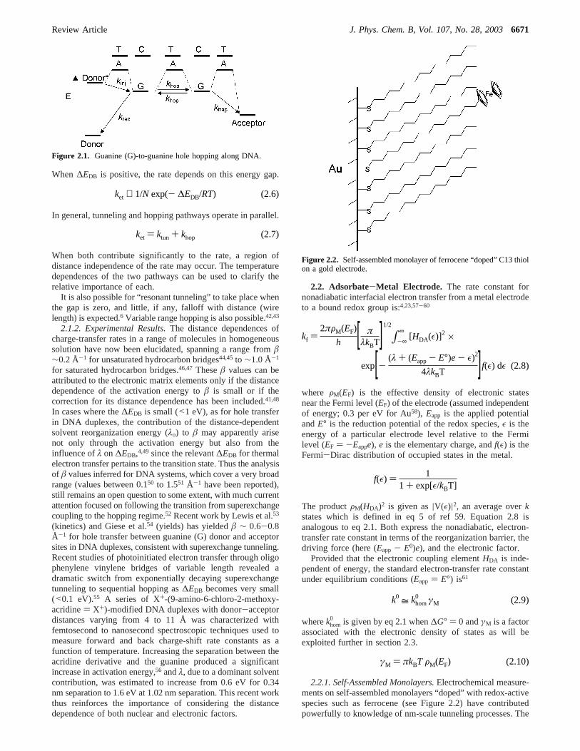
2.2. Adsorbate-Metal Electrode. The rate constant fornonadiabatic interfacial electron transfer from a metal electrodeto a bound redox group is:4,23,57-60
where FM(EF) is the effective density of electronic statesnear the Fermi level (EF) of the electrode (assumed independentof energy; 0.3 per eV for Au58), Eapp is the applied potentialandE° is the reduction potential of the redox species,ε is theenergy of a particular electrode level relative to the Fermilevel (EF ) -Eappe), e is the elementary charge, andf(ε) is theFermi-Dirac distribution of occupied states in the metal.
The productFM(HDA)2 is given as|V(ε)|2, an average overkstates which is defined in eq 5 of ref 59. Equation 2.8 isanalogous to eq 2.1. Both express the nonadiabatic, electron-transfer rate constant in terms of the reorganization barrier, thedriving force (here (Eapp - E0)e), and the electronic factor.
Provided that the electronic coupling elementHDA is inde-pendent of energy, the standard electron-transfer rate constantunder equilibrium conditions (Eapp ) E°) is61
wherekhom0 is given by eq 2.1 when∆G° ) 0 andγM is a factor
associated with the electronic density of states as will beexploited further in section 2.3.
2.2.1. Self-Assembled Monolayers.Electrochemical measure-ments on self-assembled monolayers “doped” with redox-activespecies such as ferrocene (see Figure 2.2) have contributedpowerfully to knowledge of nm-scale tunneling processes. The
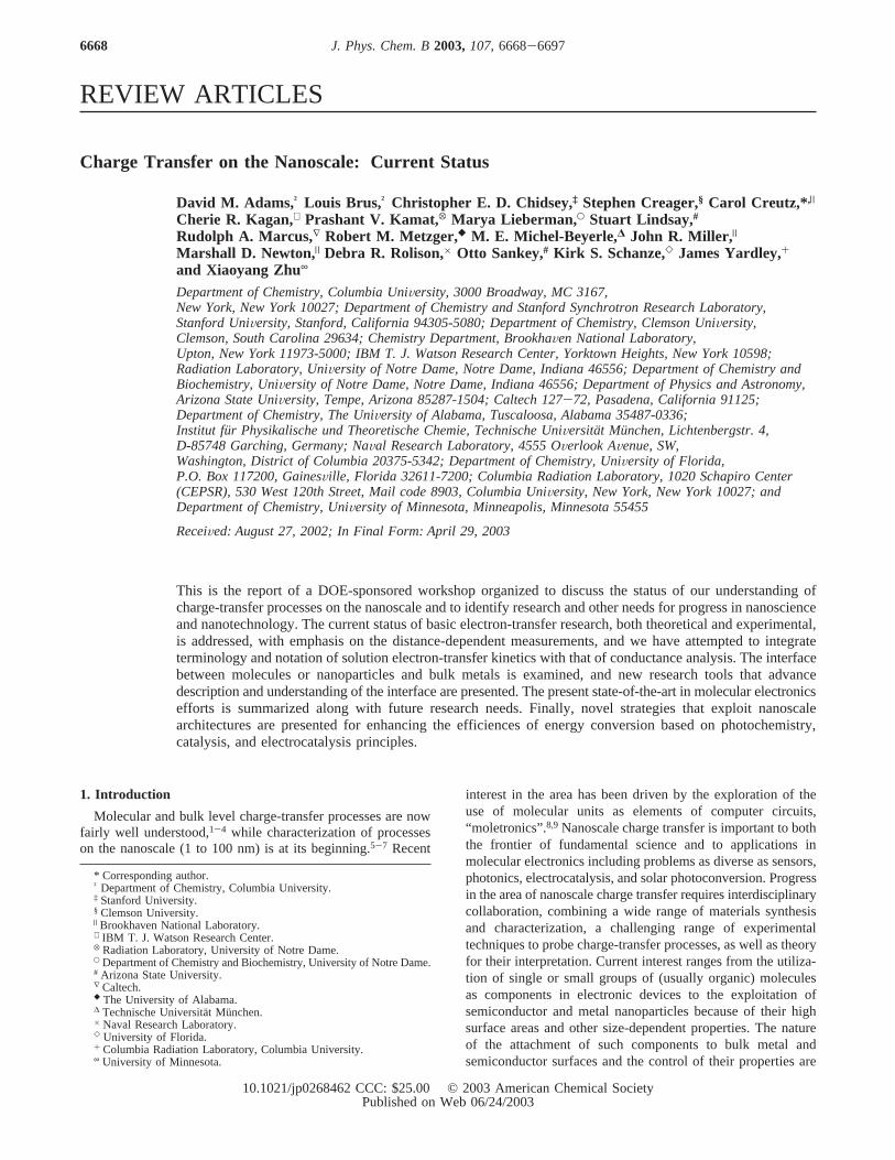
Figure 2.1. Guanine (G)-to-guanine hole hopping along DNA.
ket ∝ 1/N exp(- ∆EDB/RT) (2.6)
ket ) ktun + khop (2.7)
Figure 2.2. Self-assembled monolayer of ferrocene “doped” C13 thiolon a gold electrode.
kf )2πFM(EF)
h [ πλkBT]1/2
∫-∞
∞[HDA(ε)]2 ×
exp[-(λ + (Eapp- E°)e - ε)2
4λkBT ]f(ε) dε (2.8)
f(ε) ) 11 + exp[ε/kBT]
k0 = khom0 γM (2.9)
γM ) πkBT FM(EF) (2.10)
Review Article J. Phys. Chem. B, Vol. 107, No. 28, 20036671

interfacial electron-transfer processes studied involve a metalelectrode and a molecular unit (entry 2 in Table 1) inself-assembled monolayers, typically composed of thiols boundto gold. The exponential distance dependence ofket has beendemonstrated for organic thiols as a function of length and thenature of the bridge (e.g., alkane vs aromatic), yielding resultssimilar to those inferred from homogeneous electron transfer(above). For alkanes,â lies in the range 0.9-1.3 per Å;23,60,62
for oligophenylene,â is smaller, 0.4-0.5 per Å.63-65 (Ref 27reviews the recent literature.)
2.2.2. Localized Charge Generation and Ion Motion.Chargetransfer in classical chemical systems involves motion of ioniccharges, often via a combination of long-range electron transferand counterion motion. The overall reaction driving force andrate in such systems are greatly affected by the electrostaticinteractions of ions with their local environment and with eachother. Charge balance is usually simple because no electronsor ions are added from external sources, and one can usuallyconsider the system in isolation.
In electrochemical systems the situation can be more complex.Fixed charges are generated by electron transfer to/from anelectrode, and charge-compensating counterions are generatedat another electrode that is usually positioned far away. Theimportant electrostatics are those associated with the electro-generated ion and its local environment, and with the charge-compensating counterion(s) that may or may not be present inthe region near where the ion is generated. Generation of anion in a place that is isolated from ions of opposite charge isenergetically costly, and that cost affects the energy requiredto generate the ion.66,67 The energetic cost is diminished ifcounterion(s) can come close to the electrogenerated ion, but ifthat process is slow then it can limit the overall rate of chargetransfer.
These ideas are illustrated in recent work by Sumner and co-workers (see Figure 2.3) involving an electrochemical systemin which a redox molecule (ferrocene) is positioned in a self-assembled monolayer on a gold electrode in a microenvironmentthat does not permit access of counterions to the redoxmolecule.68 Charge transfer between ferrocene and gold isdramatically slowed when the ferrocene is “buried” in ahydrophobic pocket into which anion access is inhibited. Incontrast, direct exposure of the ferrocene to the contactingelectrolyte increases the ferrocene oxidation/reduction rate byover 2 orders of magnitude, despite the fact that the molecular“bridge” connecting ferrocene to gold is the same in both cases.
These results highlight the coupled nature of electron andion transport in chemical systems on nanoscopic distance scales.Several microscopic mechanisms could be envisioned by whichthis coupled electron/ion transfer reaction could occur; someof them are illustrated in Figure 2.4. A critical question iswhether one should consider the ion transport step as a coupledchemical reaction that occurs separately from electron transfer(i.e., a two-step process), or as one component of an overallreaction coordinate involving both electron and ion transfer (i.e.,a concerted process).
Effects of counterions have also been seen on rates of long-range electron transfer in nonelectrochemical systems, and thesehave been modeled in several ways.69 For example, Barnett andco-workers report that thermal motions of hydrated sodiumcounterions can strongly affect hole transport along DNA doublehelices in solution.70 In their experiments, hole transport alongnative B DNA oligomers was compared with that alongcomparable oligomers that had been modified to incorporateNa+-starved regions into the double-helix region between thecharge injection point and the GG site to which the injectedholes ultimately migrate. The extent of hole migration was muchless for the Na+-deficient oligonucleotides than for the nativeoligonucleotides, in agreement with simulations which suggestthat hole transport is coupled to stochastic fluctuations in thecounterion spatial configurations. This work and the work bySumner et al. highlight the manner in which electron (hole) andion dynamics can become coupled in systems where chargeexists in localized states.
2.3. Metal/STM Tip-Molecule-Metal Electrode. In con-trast to homogeneous and interfacial electron transfer, in which
Figure 2.3. The standard electron-transfer rate constant for ferrocene oxidation/ferricenium reduction in the structure at left is 200 s-1, whereasthat for the structure at right is 40,000 s-1. The differences in rate for the two C13 thiols are closely correlated with the nature, particularly the size,of the electrolyte anions.
Figure 2.4. Mechanistic schemes for coupled electron/ion transfer inmetal-bridge-redox molecule structures.
6672 J. Phys. Chem. B, Vol. 107, No. 28, 2003 Adams et al.

a rate constant is the experimental quantity sought for motifs 3and 6 in Table 1, resistance or conductance (reciprocal of theresistance) is the experimental parameter. The conductance isgiven by the Landauer71 formula, which relates the linearconductanceg of a contact-(molecular bridge)-contact systemto the electron transmission coefficientT:
whereEF is the Fermi level of the contacts at zero voltage bias.ForT ) 1, g ) 2e2/h ) (12.9 kΩ)-1, the maximum conductanceper molecule. In principle, the distance dependence of theconductance (like that for the rate constant) can be exponential
or “Ohmic”
where (as above)N is the number of repeated residues (e.g.,CH2, etc.).
2.3.1. Experimental Studies.Several types of “MIMs” (metal-insulator-metal) have been devised and studied, with the goalof characterizing the conductance of the (usually organic)molecule. In “break” junctions single molecules are trappedbetween metal electrodes.24,72 Self-assembled monolayers asdescribed in section 2.2 are interrogated with scanning tunnelingmicroscopy in dry N212 or under a solvent. Self-assembledthiolate monolayers on gold were probed as a function of thiolatewith the gold tip of a conducting AFM probe, andâ factors of0.42 Å-1 and 0.96 Å-1 were found for oligophenylene andalkane, respectively.28 This distance dependence (measured inthe presence of dry N2) is similar to that found for theelectrochemical solution measurements obtained for aqueousmedia (somewhat surprising, given the potentially large shiftin energies on changing the surrounding environment). Woldand Frisbie found electronic transport across all-trans alkylchains (in the absence of solvent) to depend critically on whetherthe chains are chemically bound to the electrodes or not in metal/molecule/p-type semiconductor junctions; tunneling of holes inthese semiconductor-containing systems is more efficient thanthat of electrons; indeed, hole tunneling inσ-bonded chainsappeared similar to electron tunneling through conjugated ones.73
The configuration shown in Figure 2.5 has been used to makeconductance measurements at more than 4000 “single-molecule”sites, where it is assumed that the alkanes are in the fully transconformation.16 Dithiol bridges were introduced into thiol self-assembled monolayers and then topped with gold nanoparticles(“Au101(PPh3)21Cl5”74) capped with triphenyl phosphine ligands.The assemblies (under toluene) were then probed with a
conducting AFM tip. The scans were stopped at nanoparticlejunctions and the conductances of individual assemblies wereprobed as a function of bias voltage, and, in some cases, lateralforce. Multiple measurements were obtained by probing differentnanoparticle junction sites.
One remarkable aspect of the system’s behavior is theappearance of 1-5 “quanta” of current. These quanta areattributed to 1 to 5 dithiols linked to the tip by the interveningnanoparticle(s). Another potential issue is the exact role of thenanoparticle, since Coulomb blockade has been observed forgold nanoparticles in the 1.1 to 2.0 nm size range.15,75 Otheraspects of the charge transport appear to be quite different fromwhat is observed in alkanethiol monolayers (by, e.g., electro-chemical or STM/AFM measurements). The absolute magnitudeof the conductance (at low bias) of molecules in metal-molecule-metal junctions is close to what can be inferred frominterfacial electron-transfer rate constants measured for relatedsystems. (See section 2.4.) However, the electronic decaycoefficient,â, is reduced below the value found for the case ofcontact to just one electrode. Corresponding to the small valueof â at small (<50 mV) bias,â at high bias (up to( 1 V)drops substantially with increasing bias. These observations aredifficult to understand. Electronic structure calculations showthat the gold Fermi level lies near the middle of the HOMO-LUMO gap,76 so that the dithiol molecular orbitals are some 5eV away from resonance. Under these conditionsâ should beabout 1.0 (per methylene) and only very weakly dependent onbias. An implication of the observed distance dependence isthat the dithiol energy levels have shifted dramatically withrespect to the gold Fermi level. This raises the issue that themetal electrodes used to contact molecular conductors may playa dominant role in conduction of the overall system, a topicdealt with in the next subsection.
2.3.2. Role of Metals in Molecular Conduction.An importantfactor that affects the current-voltage characteristics of ametal-molecule-metal system is the energy of the metal Fermilevel EF relative to that of the HOMO and LUMO levels of themolecule. At equilibrium and with no applied voltage, the Fermilevels (chemical potentials) of the two metals will coincide atenergyEF. The alignment ofEF relative to the HOMO or LUMOaffects how readily an applied bias can bring a molecular levelinto resonance with a metallic conduction state to produce anapparent large turn-on of the current. Before resonance thealignment ofEF affects the tunneling decay rateâ, and thisexponentially affects the magnitude of the current. While suchsensitivity has been suggested for the conductance data,16 itshould be noted that the analogous data for examining suchsensitivity in the electrochemical kinetics23 is not available.
Exactly whereEF lines up relative to the molecular levelsdoes not have a simple “universal” answer. The situation is quitereminiscent of the metal/semiconductor interface, which pro-duces the Schottky barrieræ. The barrieræ is the energydifference between the metal Fermi levelEF and the semicon-ductor conduction bandEc, æ ) Ec - EF. This problem hasbeen examined extensively,77 and we briefly review it here tolearn the general principles as well as the difficulties in obtaininga quantitative theory. The simplest estimate ofæ is to set thevacuum levels of the metal and semiconductor equal. Thisestimate isæ ) W - ø, where W is the metal work functionand ø is the electron affinity of the semiconductor. This so-called “Schottky limit” seldom works because it neglects thecharge transfer and rebonding at the interface, which producesinterface dipoles. Another limit is the Bardeen limit in whichEF is “pinned” at the same level for a particular semiconductor
Figure 2.5. Configuration used for multiple conductance measure-ments. (Au-S-(CH2)N-S-Au-Np-Au) where Au-NP is a ligand-capped, gold nanoparticle.
g ) 2e2
hT(EF) (2.11)
g ) g0 exp(- âdDA) (2.12)
g ∝ 1/N exp(- ∆EDB/RT) (2.13)
Review Article J. Phys. Chem. B, Vol. 107, No. 28, 20036673

for all metals. In the Bardeen limit all metals produce the samebarrier æ. This is observed in many semiconductor/metalsystems. Tersoff78 put forward a model of Fermi-level pinningfor metal/semiconductors in which the alignment is controlledby the semiconductor and has little to do with the metal. Theconcept is that the metal states with energies within thesemiconductor band gap tunnel into the semiconductor, and thetunneling behavior is controlled by the semiconductor. Thesemetal-induced band gap states are filled up to the so-called“charge neutrality level” (CNL) of the semiconductor. The CNLis where the tunneling states change from valence-band toconduction-band character. This theory has been quite successfuland qualitatively explains the data. But for some systems, ittoo fails.
A fully self-consistent electronic structure calculation is able,in principle, to determine the lineup of a metal/molecule systemsince it includes all charge redistribution effects. Xue et al.79
have used a density functional technique to study phenyldi-thiolate between Au contacts. They find that dipole effects dueto the sulfur-gold bond affect the lineup, and the results arevery encouraging. Tomfohr et al.76 followed up on the Schottkybarrier analogy and determined the charge neutrality level ofoctanedithiol. The CNL is then compared to a self-consistentelectronic structure calculation. The self-consistent alignmentof the Fermi level is found to agree well with the CNL of themolecule. This gives hope that general concepts that giveguidelines may be developed as for Schottky barriers. Clearlymore theoretical work is needed to obtain a comprehensivetheory for the lineup, anddirect comparison with experimentis lacking.
In additon to the issue of the alignment of the Fermi levelrelative to the molecular orbitals, the metal contacts can perturbthe molecular states. Clearly, overlap between metallic andmolecular states is a prerequisite of electronic coupling, andoverlap produces hybridization. This effect is usually small,much less than an eV, which is smaller than effects frompolarization and charge transfer at the interface that controlsthe Fermi-level alignments (which can shift (uniformly) statesby an eV or more in energy).80 The presence of metals is alsoimportant in determining local electric fields (see section 2.3.3).An extreme example of this is resonance Raman enhancementsowing to coupling to plasmons in metallic nanoclusters.
Electroactive molecules generally have redox-accessible statesthat lie within an eV or so of the metal Fermi level, and bondingsuch molecules to metal electrodes may modulate their con-ductivity. It is, however, surprising that significant effects areimplicated for then-alkane bridges discussed in section 2.3.1,as these are inert molecules with highly localized electronicstates. Thus, it appears that contacting these (electrochemically)inert molecules to gold electrodes at both ends may have aprofound effect on their conductivity. It could be the case thatthese metal-induced effects result from a major change in theelectronic properties of the system compared to its components.Alternatively, the changes may be caused by constraining theconducting molecule to remain attached to the electrodes,eliminating degrees of freedom available to unconstrainedmolecules. Whatever the cause, it is clear that metal contactscan play a significant role in the electronic properties of ametal-molecule-metal nanoscale system. These effects willhave to be characterized and understood, using such tools asphotoelectron spectroscopy (PES) and 2 photon ES,81 as wellas local probe measurements on well characterized assemblies.This is a necessary step in the rational design of nanoscalemolecular electronic devices that rely on metal contacts.
2.3.3. Electric Field.A concept related to that discussed insection 2.3.2 is the voltage drop profile of the metal/moleculesystem under bias and how it affects theI-V characteristics.Mujica et al.34 used a simple tight-binding model to find thevoltage profile across a molecular chain. These results are quiteinformative in that they show that the largest potential dropoccurs for atoms near the electrodes. Li et al.82 have foundsimilar results for dithiolated alkanes connected to Au, wherethe largest drop occurs between Au and the end S atoms of themolecule.
A nice model to view this behavior comes from the work ofTian et al.83 They consider the molecular levels as being fixedunder bias, while the two chemical potentialsEF
L and EFR (for
the left and right electrodes) are displaced from each other byeV, whereV is the external voltage bias. Electrons that cantransfer through the molecule are those within the “energywindow” betweenEF
L andEFR. If the molecule and its contacts
are symmetric,EFL moves down byeV/2 (EF
L ) EF - eV/2) andEF
R moves up byeV/2 (EFR ) EF + eV/2). This produces a
symmetricI-V curve (-I(-V) ) +I(+V)). At high enough bias,a molecular orbital may enter the energy window betweenEF
L
andEFR to produce a resonance and a rapid increase in current.
This rapid turn-on of the current occurs at the same magnitudeof bias for either positive or negative bias.
A symmetric situation is not the norm. Even for a symmetricmolecule the left and right chemical contacts may not be thesame; one contact may be much stronger than the other. Tianet al.83 introduce an asymmetry parameterη which raises orlowers the two-electrode Fermi levels (relative to the molecularlevels) at different rates under bias,EF
L ) EF - ηeVandEFR )
EF + (1 - η)eV. The difference betweenEFL andEF
R is eV asrequired. This asymmetry parameter can produce a veryasymmetric I-V curve. To see this, suppose we have a moleculewith a 3 eV HOMO-LUMO gap, and suppose that the twometal electrodes line up their Fermi levels atEF, which is+1eV above the HOMO (or equivalently 2 eV below the LUMO).Consider the extreme case ofη ) 0. This means that the Fermilevel of the left electrode is “locked” onto the molecular levels,while the right metal electrode Fermi level floats up or downexactly in line witheV. This might model a system with a strongchemical contact with the left electrode and a weak one for theright. If we apply a bias of+1 V, the energy window betweenEF
L and EFR ranges from 1 to 2 eV above the HOMO (or
equivalently 2 eV to 1 eV below the LUMO). The situationchanges drastically under reverse bias. Reverse the bias to-1V. The energy window now ranges from 1 eV to 0 eV abovethe HOMO (2-3 eV below the LUMO). Since the energywindow here has just captured the HOMO, we open up aresonant channel for conduction and the current becomes verylarge. Instead of theI-V being symmetric, we instead findrectifying-like behavior: a large current (due to resonance withthe HOMO) with one bias, and little current (no molecularorbital resonance) for the opposite bias. Such rectifying behaviorof an asymmetrically coupled molecule has recently beensimulated using the advanced nonequilibrium Green’s functiontechnique.84
The magnitude of the field in reportedI-V measurements isin the range of 107 - 109 V/m. (The field used routinely inStark (electroabsorption) experiments is 107-108 V/m.) Thefield used for theI-V measurements is comparable to thatcommon in electron-transfer solution experiments: for aD-B-A assembly in a solvent of dielectric constant Ds
undergoing charge transfer from negatively charged D to neutralA separated bydDA ) 1 nm, the field across the molecule is
6674 J. Phys. Chem. B, Vol. 107, No. 28, 2003 Adams et al.
109/Ds V/ms107 to 109 V/m, depending on the solvent used.As described above, the field need not, and generally will not,be uniform across the molecule, and likely there is a reducedfield within the molecule and a significant enhancement of thefield at the metal/molecule interfaces.
2.4. Comparison between Electron-Transfer Kinetics andConductance in Metal-Bridge-Metal (MBM) Junctions.The kinetics of electron (or hole) transfer between localizedmolecular donor and acceptor sites, mediated by a molecularbridge or spacer (eq 2.1) or in the related interfacial electron-transfer process (eq 2.9), shares many features with conductancein related metal-bridge-metal (MBM) junctions. Guided byappropriate dynamical models,29-33,85,86 it is important toappreciate the similarities as well as significant differencesbetween the two types of charge-transfer process. While a givenDBA entity may be common to both processes, many detailsof the system may differ, including the nature of the initial andfinal states and the “reservoirs” to which the D and A sites arecoupled.29,30,86 It has been proposed recently31,85 that theLandauer expression (eq 2.11), initially introduced to accountfor coherent electron tunneling, can be reexpressed and general-ized as follows:
where the electron-transfer rate constantket, defined by con-sidering steady-state charge transport (ket ) kss), may includein parallel both coherent tunneling through the bridge (ktun) andincoherent hopping initiated by thermal charge injection ontothe bridge (khop) and whereFi(EF) is the initial electrode densityof states (introduced asFM(EF) in eq 2.9):
We consider now the special limitket ) ktun which occurswhen the energy gaps between resonant initial and final statesand an intermediate charge-transfer state involving the bridgeare sufficiently large. In this case the bridge-mediated tunnelingmay be described by superexchange tunneling, as discussed insection 2.1.1.87 Dealing first with the DBA system in isolation,we may express the rate constant for electron transfer betweenD and A,ket, as eq 2.1, and more generally we may write
where DOS is the effective density of states associated withthe standard Golden Rule formulation of the rate constant. Forhomogeneous electron transfer, DOS corresponds to FCWD,the Franck-Condon weighted density of vibronic states control-ling activated electron transfer when D and A sites are coupledto vibronic reservoirs (eq 2.1).29,32,33For electron transfer froma molecular adsorbate to a metal electrode, the FCWD due tothe electrolyte phase, as well as the molecular modes of theDBA system, is supplemented by an additional factorγΜ, dueto the electronic manifold of the metal23,60,62,88(eq 2.10).
When∆G° ) 0, Franck-Condon weighted density of states
From eq 2.10, withkBT ) 0.026 eV (298 K) andFM(EF) ) 0.3eV-1 for a gold electrode,52,89 γΜ ) 0.024.
The simple McConnell superexchange model (for nearest-neighbor or tight-binding coupling among D, A, and bridge sites)may be expressed as29,30,32,33
where the D and A sites are coupled, respectively, to the sites1 andN of the bridge (taken as a linear sequence ofN sites)and G1N(ED) is the Green’s function of the bridge, evaluatedat the energy of the donor stateED. Note that the couplingbetween D and A is indirect through the bridge, so that thereis no direct coupling between the two. Instead, higher orderperturbation theory is needed, which is exactly solved by theT-matrix, T ) H + HGH, leading in the present case toHDA (as in eq 2.19)) TDA ) HD1G1N(ED)HNA.90
In dealing with the larger context of an MBM junction, onemay attempt to maintain the identity of the DBA moietyinvolved in the electron transfer (eq 2.1 or 2.9), as Nitzan hasdone,32 but now providing for the coupling of the D and A sitesto metal electrodes (i.e., electronic reservoirs; at the same time,the vibronic reservoirs so central to electron-transfer kineticsmay be absent or of much less significance29,30). In effect, themodel for the isolated DBA systems is broadened to includethe additional “donor” and “acceptor” sites provided by themetal electrodes. We thus have an extended Green’s function,GDA(EF) which includes the D and A sites as well as theNsites of B:29,30,32,33
If the D and A energies (ED, EA) are assumed to be quite closeto the metal Fermi energy (EF) (e.g., as a result of strong contactinteractions32), it is essential to include the so-called “self-energies”,ΣD and ΣA (generally complex), which reflect theinfluence of the metal reservoirs. Discrete levels of the molecularbridge are resonant with the metal continuum of states. Theinitial molecularδ-function density of states broadens into acontinuous local density of states spectrum with peaks andwidths described byΣ. The self-energies are also crucial if thebridge sites approach resonance withEF.29,30 The over bars ineq 2.20 allow for the fact that incorporating DBA into thejunction may modify the electronic structure,31-33,85 althoughsuch effects are not included in the treatment below. In termsof GDA, the conductance may be expressed as,29,32
where the “widths”Γ (the imaginary components ofΣ) reflectthe strength of the M-D and A-M coupling. Nitzan has pointedout32 that whenΣ is dominated by itsΓ component (as mightbe expected for strong chemisorptive coupling), then thefollowing simple relationship betweeng andket emerges (subjectto various assumptions32):
Making the plausible assumption thatΓD ) ΓA ∼ 0.5 eV yieldsthe order of magnitude relationship
g ) e2ket (EF)Fi(EF) (2.14)
ket) ktun+ khop (2.15)
ket) (4π2/h)|HDA|2DOS (2.16)
DOS) γΜ(FCWD) (2.17)
FCWD ) [ 14πλkBT]1/2
exp[- λ4kBT] (2.18)
HDA ) (HD1)(HNA)G1N(ED) (2.19)
GDA(EF) )HD1HNAGh 1N(EF)
(EF - ED - ΣD(EF))(EF - EA - ΣD(EF))(2.20)
g(EF) ) (2e2
h )|GDA(EF)|2 ΓD(EF)ΓA(EF) (2.21)
g ∼ 8e2
π2ΓDΓA
( ket
DOS) (2.22)
g ∼ 5 × 10-19ket/DOS (2.23)
Review Article J. Phys. Chem. B, Vol. 107, No. 28, 20036675

where the units ofg, ket, and DOS are, respectively, reciprocalohms (Ω-1), seconds (s-1), and electronvolts (eV)-1. In eqs 2.22and 2.23,ket is taken asktun (see eq 2.15).
As an alternative to the limiting case described above (whereΣ is dominated byΓ, due to the near resonance of the D and Alevels with the Fermi level) we may adopt a model ofconductance in which the explicit presence of D and A sites isdropped and the bridge is taken as being directly coupled togeneralized donor and acceptor sites, including the metalelectrodes.31 If the coupling is characterized byHLB andHBR,and the metal density of states byFL andFR (where L and Rdenote the “left” and “right” electrodes), one obtains
(by analogy with the notation in eq 2.21, “widths”ΓL or ΓD
may be defined asΓL ) FLHLB2 andΓR ) FRHBR
2 ). If the ratioof Hs is taken as order of unity andFL, FR ∼ 0.3 eV-1 (asalready adopted above for gold following eq 2.18), we obtain
(A related analysis has been discussed in ref 31.)Equations 2.23 and 2.25 provide a convenient approximate
basis for comparing estimates ofg andket involving a commonbridge unit. As an example, Table 2 offers experimentalconductance and electrochemical kinetics results16,60,62,91,92basedon charge transfer through linear chains comprised ofNframework atoms (N ) 8, 10, or 12) of types (CH2)N,C(O)NH(CH2)N-2, C(O)O(CH2)N-2, all of which have similarlengths (for a given value ofN). In the conductance experi-ments16,92alkane bridges are terminated by thiolate groups linkedon one end to a planar gold electrode and on the other to agold nanocluster through which contact to the conducting atomicforce microscope (AFM) tip is made. In the electrochemicalket
measurements,60,62,91one end of the bridge is linked to a goldelectrode by a thiolate group, and the other end is linked to aferrocene group. Thus, in all cases, both bridge termini arecovalently linked to their outer neighbors.
Table 2 indicates that the limiting theoretical model repre-sented by eq 2.23, i.e., with D and A levels nearly resonantwith the Fermi level, accounts for the observed transport datato within about 1 order of magnitude, a result which may beconsidered quite satisfactory given the assumptions involvedin the model and the fact that the various experimentally studiedsystems, despite their generic similarities, do exhibit chemicaldifferences. The alternative (nonresonant) model given by eq2.25 yields appreciably smaller predictedg values lying belowthe experimental values by factors ranging from 30 (n ) 8) to400 (n ) 12).16,92 Corresponding to the intriguing fact that thefalloff of g with n (1.8 per CH2 group92) is appreciably more
gradual than observed in theket data (∼3-4 per CH2 group60,62,88),the calculated ratio ofg to ket increases by an order of magnitudeover the rangen ) 8 to 12. This difference in falloff ratessuggests important sensitivity of the transport rate to details ofthe contacts between the components of the junctions.16,92Thepresence of the gold nanoclusters in the conductance studiesmay also play a role.
Comparisons may also be made for unsaturated bridges. Forexample, the scaledket value (eq 2.23) for electron transferthrough an oligophenyleneethynylene bridge (a)63 is within anorder of magnitude ofg for conductance through an oligo-phenylene bridge (b)93 in a case where the two systems havesimilar overall metal-metal separations (∼18-20 Å, corre-sponding respectively to two phenyleneethynylene units andthree phenylene units).
2.5. Calculation ofâ. Theory and computation are essentialto interpretation of electron transport mechanisms. The super-exchange description has been widely used for molecularelectron-transfer processes in solution.40 At the heart of thesecalculations is the calculation of the molecular Green’s function,also know as the propagator. The quantum mechanical propaga-tor describes the propagation of an electron of a given energythrough the molecule.
2.5.1. Calculation ofâ with a Recursion Relation.A recursionrelation has been formulated for the Green’s function forcalculating the effective electronic coupling in bridge-assistedelectron-transfer systems, within the framework of the tight-binding Hamiltonian.94 The recursion expression relates theGreen’s function of a chain bridge to that of the bridge that isone unit less. It is applicable regardless of the number of orbitalsper unit. This method has been applied to a ferrocenylcarboxy-terminated alkanethiol on the Au(111) surface. At largernumbers of bridge units, the effective coupling strength showsan exponential decay as the number of methylene (-CH2-)units increases. This sequential formalism shows numericalstability even for a very long chain bridge and, since it usesonly small matrices, requires much less computer time for thecalculation. Identical bridge units are not a requirement, so themethod can be applied to more complicated systems.
2.5.2. Calculation ofâ with a Complex BandstructureApproach. A complex bandstructure approach has recently
TABLE 2: Comparison of Experimental g(Ω-1) and kEt (s-1) Data for Alkane Chain-Mediated Charge Transfer
alkane bridgea
(X(CH2)n-2) g (Ω1-)b5 × 10-19ket/DOSc
(eq 2.23)8 × 10-21ket/DOSc
(eq 2.25)
n ) 8 (10.3( 0.5)× 10-10 2 × 10⁻⁸ 3 × 10-11
n ) 10 (3.5( 0.2)× 10-10 (2 ( 1) × 10-9 (3 ( 1) × 10-12
n ) 12 (1.2( 0.1)× 10-10 (2 ( 1) × 10-10 (3 ( 1) × 10-13
a X ) (CH2)2 in the conductance measurements16,92and some of the electrochemicalket measurements.91 In other electrochemical measurements,X is an amide62,91(C(O)NH) or ester60 (-C(O)OC) moiety.b In the conductance measurements16,92D and A thiolate groups are coupled, respectively,to a planar gold electrode surface and a gold nanocluster.c In the electrochemical60,62,63,91ket measurements, the D and A groups are, respectively,a thiolate linked to a gold electrode surface and a ferrocene group. The room-temperature FCWD was evaluated on the basis of a classical modelusing a value of 0.9 eV for the reorganization energy (FCWD)) exp(-λ/4kBT)/(4πkB Tλ)1/2 ) 2.95× 10⁻⁴ eV-1).60,62,91A value of 42 was usedfor 1/γΜ (see eq 2.10).
g ) e2
2π2( ket
DOS)(HLB2 HBR
2
HDB2 HBA
2 )(FLFR) (2.24)
g ∼ 7 × 10-22ket/DOS (2.25)
6676 J. Phys. Chem. B, Vol. 107, No. 28, 2003 Adams et al.

proven valuable in interpreting the conductances of alkanedithiols bridging a gold electrode and an AFM tip.16,92 Thecomplex bandstructure of a periodic system is the conventionalbandstructure extended to complex Blochk vectors. Thekvectors with an imaginary part describe spatially decaying wavefunctions and arise in, for example, the analysis of impurityand surface states. They also represent the quantum tunnelingstates, which are vehicles of electron transport through a barriersuch as a thin oxide layer or a molecule. Plots of the band energyas a function of the distance decay coefficientâ are used todetermine which bands have sufficiently small values ofâ tobe effective in long-range transfer. For alkane, alkene, andbenzene chains the following results were obtained76 providing
a direct link with experiment. The form of the complexbandstructure clearly elucidates the molecule length dependenceof the tunneling current. In formulas such as eqs 2.19 or 2.21,the effect of tunneling manifests itself through the Green’sfunction, which depends on the electron’s energy within theHOMO-LUMO gap of the bridge. The Green’s function cantheoretically be composed of a sum of contributions from Bloch-like wavevectors, with the wavevectors being complex (expo-nentially damped instead of oscillating). For long molecules,one need only keep the smallest complex wavevector (thesmallestâ value) to arrive at a simple, yet exact in principle,method to estimate the Green’s function. The structure of thecomplex bandstructure also suggests a scheme to align the Fermilevel of the metal with the molecular orbital energies, similarto Schottky barrier alignment in metal semiconductor systems.
2.6. General Issues for the Future.2.6.1. Methods forCollection of Statistically Significant Data Sets. Many studiesof the conductance of molecules (entry 3 in Table 1) have beencarried out one molecule at a time. It is desirable to be able toefficiently collect sets of data for a large number of molecules.Utilization of self-assembled monolayers offers one solution tothis problem,15,16,95 but other approaches, such as use ofpatterned electrode arrays onto which the molecules of interestcould be adsorbed, need to be in wide use.
2.6.2. Coupled Electron and Ion Motion.Charge transfer inclassical chemical systems involves motion of fixed ioniccharges, often via a combination of long-range electron transferand counterion motion. The overall reaction driving force andrate in such systems are greatly affected by the electrostaticinteractions of ions with their local environment and with eachother. Charge balance is usually simple since no electrons orions are added from external sources, and one can usuallyconsider the system in isolation. As discussed in section 2.2,electrochemical systems are more complex because charges dueto electron transfer may be generated at one electrode whilecharge-compensating counterions are generated at anotherelectrode that is usually positioned far away. The coupled natureof electron and ion transfer is certain to be important in manyother nanoscale systems involving charge transfer. This willinclude nearly all systems utilizing nanoscale materials in energy
conversion, for example, in battery and fuel-cell electrodes andgalvanic photoelectrochemical devices. Energy conversion insuch devices nearly always involves creation and/or motion ofcharges, therefore energy conversion will always be fastest andmost efficient when charges can be generated and movedwithout high energetic cost. This idea is quite general, such thatany nanoscale system which transports charge by a site-to-sitehopping mechanism should be strongly affected by the energet-ics of ion generation and motion. The coupled nature of electronand ion hopping is widely recognized for charge transport inbulk materials such as redox polymers,96 and the ideas that haveevolved to describe charge transport in such systems shouldtranslate well to nanoscale systems.
In some nanoscale systems involving charge transfer, thesituation is less clear. For example, consider the case of chargetransfer between two metal electrodes connected via a singlebridging molecule. Charge transfer can occur across such a two-terminal structure in the absence of electrolyte or solvent withoutever generating a fixed charge; thus, the energetic cost ofgenerating and moving ions is expected to have relatively littleeffect on the rate (current). In such a structure, charge transportcould also occur by a hopping mechanism involving transientcreation of charged sites on the bridge. Three-terminal moleculardevices in which a third electrode is brought into close proximityto an electron donor or acceptor in the bridge to achieve controlover the charge transfer across the bridge are also of interest,primarily for applications in molecular electronics and infor-mation processing. It seems likely that the energy associatedwith forming and transporting ionic sites could be importantin such structures. The question of how one should think aboutthe charge balance in such structures is an open one, sinceionic sites are presumably generated but charge-compensatingcounterions need not be present to transport charge. Thesesystems present an opportunity for improved understanding ofcharge transport on the nanoscale.
Metal nanoparticles and nanoparticle arrays comprise anothernanoscale system in which fixed ionic sites may effect chargetransport. Metal nanoparticles can transport charge by a hoppingmechanism involving transient charging of the nanoparticle(treating the particle as a nanoscale capacitor)97,98 and/or by ametal-like transport mechanism involving significant electrondelocalization among the particles.99 Particle size and spacing,the dielectric properties of the medium in which the particlesare immersed, and the presence of free ions (electrolyte) in thelocal medium will be crucial to the behavior of such materials.A unified picture of charge transport in such materials has notyet emerged, and the development of such a picture constitutesanother significant opportunity in the area of nanoscale chargetransfer.
3. Electron Transport at Interfaces
Although there are many manifestations of charge transportat interfaces, the nature of electron transport at the interface ofa metal with a single molecule or molecular nanostructure iscritically important for understanding a broader array ofinterfacial phenomena and for many technological issues. Forexample, the drive toward electronic processing of informationinto the nm dimensional regime will require a major shift fromcurrent silicon-based MOS device structures. Molecular andnanoscale organic materials offer a potential new paradigm, butour understanding of these phenomena is limited. Many of theproposed schemes for a molecule-based nanoelectronic devicerequire making electronic contacts to one or a group ofmolecules.100-108 In this regard, electronic interaction between
Review Article J. Phys. Chem. B, Vol. 107, No. 28, 20036677

a metal electrode and a molecule determines not only contactresistance but also the functional nature of the molecular device.For a small molecule contacted by two metal electrodes, thecomplete system could be regarded as an interface problem.The transfer of electrons through such interfaces can also directlyinfluence the effectiveness of energy conversion processesimportant to advanced fuel cell development, solar energyharvesting, or photocatalysis.
From scattering theory, the electrical conductance (g) for asingle molecular orbital coupled to two electrodes may bedescribed through the expression (which is equivalent to eq 2.21in section 2.4)29,30
wheregc () 2e2/h) is the quantum of conductance;∆L and∆R
represent the electronic coupling strength between the molecularorbital and the left and right electrodes, respectively; andG isthe Green’s function matrix element for the molecular bridge.This approach separates the problem into two parts: the contactproblem and the bridge problem. This formalism clearly showsthat the contacts are as important as the molecular structure ingoverning electron transport.109,110 In reality of course, themolecular bridge itself can be strongly influenced by and notstrictly separable from the contacts.79
The conceptual starting point for treating the contact can bethe Newns-Anderson chemisorption model,111,112but the one-dimensionality of the metal in this model is a significantlimitation. An improvement treats the metal electrode as a semi-infinite continuum, the so-called “jellium” model.113More recenttreatments employ atomistic models of contacts and reveal thesensitivity of interfacial electron transfer to structural details ofthe contact, such as surface coordination number, bond distance,symmetry, and chemical identity.114,115These structural factorsdetermine the electronic configurations of the interfaces. Alimitation for all of these theoretical approaches is the absenceof dynamics, i.e., the time scale for electron transfer andelectron-nuclear coupling. An accurate account of dynamicfactors will necessitate inclusion of the breakdown of the Born-Oppenheimer approximation.
Here we briefly examine the key issues involved in interfacialelectron transfer mainly from an experimental perspective andfor metal-molecule and metal-nanoparticle assemblies in theabsence of solvent and electrolyte. We illustrate some directionsand concepts for elucidating these issues: (1)Structure- whatatoms are present at the interface and where are they located?(2) Electronic configuration- what are the electronic states ofthe molecules at the interface and how are they coupled to theelectronic states of the metal? (3)Dynamics- what is the timescale for electron transport and for response of the system tothe electron transport?
3.1. Structure at the Metal-Molecule Interface.Molecularsystems are strongly influenced by interaction with differentphases present at an interface. To the extent that the Born-Oppenheimer approximation is suitable for describing molecularsystems, it is critical to know how the atomic species areconfigured as a first step toward defining the electronicconfigurations of these species. We also recognize that the localenvironment, whether gaseous or liquid or solid, does and caninfluence very strongly the atomic configurations.
The development of scanning probe microscopy (SPM),particularly scanning tunneling microscopy (STM), has revo-lutionized our capability to determine experimentally molecularconfigurations at interfaces, and many studies have demonstratedthe efficacy of these techniques. As an illustration, Figure 3.1
shows STM images of pentacene molecules at monolayer andmultilayer coverages on the Au(111) surface. The strongmolecule-metal interaction leads to the formation of a newmolecular lattice structure:π-stacking, as opposed to theherringbone structure observed for the bulk pentacene crystal.Note that these images reveal the density of electronic stateswith submolecular resolution, but an actual determination ofnuclear coordinates and chemical identity is not such an easytask. Recent experiments on inelastic tunneling with STM haveallowed the recording of vibrational spectroscopy of singlemolecules on metal surfaces.116 This development provides apowerful means of structural determination on the singleadsorbate level. However, SPM techniques are of limited usewhen the substrate deviates from a flat, single-crystal surface.
Other bulk-based probes, such as X-ray absorption finestructure, X-ray photoelectron diffraction, and electron diffrac-tion, are also sensitive to interfacial structure, but thesetechniques provide ensemble averages. Although these tech-niques are useful and can provide detailed information onmolecular configuration at well-defined interfaces, it remains agreat challenge to obtain similar levels of understanding formolecular configurations at interfaces useful for nanoscaleelectron transport, particularly when the interface is buried, suchas in a metal-molecule-metal device. The knowledge ofmolecular configuration in such a “sandwich” is critical to theinterpretation of experimental observations in molecular devices,such as the negative differential resistance observed re-cently.102,103 However, we may need to infer this knowledgefrom model molecule-metal systems until breakthroughs inexperimental techniques are found.
3.2. Electronic Configuration at the Metal-MoleculeInterface. Given a molecular configuration on a metal surface,we need to understand and describe the electronic structure ofthe coupled metal-molecule system. In some cases it maysuffice to describe the electronic configuration of the molecularsystem and then to understand the couplings of this system withthe metal. In other cases, especially where covalent bondingbetween the molecule and the metal occurs, this may beinsufficient and a complex description is necessary. Key issuesinclude (a) the extent of charge redistribution due to adsorptionand the resulting surface dipole; (b) the alignment of molecularorbital (MO) energies to the metal Fermi level; and (c) thestrength of electronic coupling (wave function mixing) betweendiscrete molecular orbitals and continuous metal bands. Chargeredistribution at the molecule-metal interface produces anelectrostatic field. Such an electrostatic potential rectifiesinterfacial electron transport; this is similar to the rectifyingeffect of a Schottky barrier. Moreover, at the nanometer scaleof concern here, these fields may strongly influence energy
g ) gc∆L∆RG2 (3.1)
Figure 3.1. Molecular resolution STM images of flat-lying pentacenemonolayer (left) andπ-stacked multilayer (right) on the Au(111)surface. The scale bar is 10 Å. The molecules are vapor deposited ontothe surface in ultrahigh vacuum at a substrate temperature of 25°C.(J.-H. Kang and X.-Y. Zhu).
6678 J. Phys. Chem. B, Vol. 107, No. 28, 2003 Adams et al.
levels within molecular units that are not directly involvedin bonding. Experimentally, this kind of interfacial chargeredistribution can be probed by surface work function measure-ments.
The energetic position of molecular orbitals with respect tothe Fermi level determines the so-called charge injectionenergetics in molecule-based electronic or optoelectronic de-vices. Beyond the immediate contact, a precise knowledge ofthis energetic alignment is critical to a successful understandingof charge transport mechanisms, including molecular orbital-assisted tunneling, resonant charge hopping, and band-likeballistic transport. Experimentally, energetic positions of oc-cupied and unoccupied molecular orbitals of adsorbates can bedetermined by photoelectron spectroscopies, including one-photon photoemission, inverse photoemission, and two-photonphotoemission spectroscopy. Alternatively, scanning tunnelingspectroscopy is capable of determining both occupied andunoccupied MOs on surfaces with spatial resolution on the Åscale.117,118
Perhaps the most important issue regarding interfacial elec-tronic configuration is the electronic coupling (wave functionmixing) between a molecule and a metal surface, i.e., the∆terms in eq 3.1. The extent of electronic coupling determinesnot only the energetics discussed above but also the dynamicsof interfacial electron transfer. Electronic coupling has beentraditionally difficult to quantify experimentally, but the recentdevelopment of two-photon photoemission (2PPE) spectroscopyhas shed light on this issue.81 The inset in Figure 3.2 illustratesthe principle of 2PPE. The interaction between a molecularorbital (MO) and the metal band structure is illustrated by amixed wave function, with the major part of the wave functionlocalized to the molecule and a minor oscillating tail in theperiodic substrate lattice. This tail is a quantitative measure ofelectronic coupling. The first photon excites an electron froman occupied metal state to the mixed molecular state; this iselectron transfer from the metal to the molecular resonance. Thesecond photon ionizes the transient molecular anion for detec-tion. The kinetic energy of the photoemitted electron providesthe energetic position of the molecular orbital. The rate ofphotoemission in this mechanism is proportional to the squareof the amplitude of the transition dipole moment (metal-to-molecule electron transfer) or the square of the amplitude of
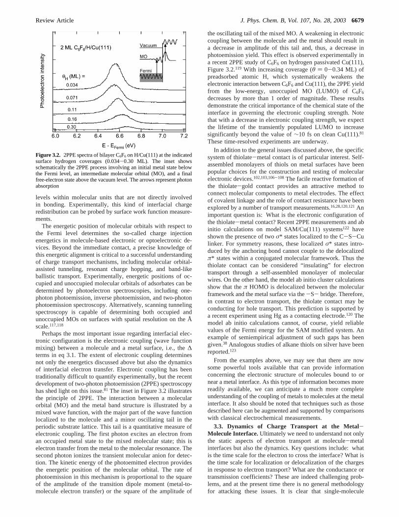
the oscillating tail of the mixed MO. A weakening in electroniccoupling between the molecule and the metal should result ina decrease in amplitude of this tail and, thus, a decrease inphotoemission yield. This effect is observed experimentally ina recent 2PPE study of C6F6 on hydrogen passivated Cu(111),Figure 3.2.119 With increasing coverage (θ ) 0-0.34 ML) ofpreadsorbed atomic H, which systematically weakens theelectronic interaction between C6F6 and Cu(111), the 2PPE yieldfrom the low-energy, unoccupied MO (LUMO) of C6F6
decreases by more than 1 order of magnitude. These resultsdemonstrate the critical importance of the chemical state of theinterface in governing the electronic coupling strength. Notethat with a decrease in electronic coupling strength, we expectthe lifetime of the transiently populated LUMO to increasesignificantly beyond the value of∼10 fs on clean Cu(111).81
These time-resolved experiments are underway.In addition to the general issues discussed above, the specific
system of thiolate-metal contact is of particular interest. Self-assembled monolayers of thiols on metal surfaces have beenpopular choices for the construction and testing of molecularelectronic devices.102,103,106-108 The facile reactive formation ofthe thiolate-gold contact provides an attractive method toconnect molecular components to metal electrodes. The effectof covalent linkage and the role of contact resistance have beenexplored by a number of transport measurements.16,28,120,121Animportant question is: What is the electronic configuration ofthe thiolate-metal contact? Recent 2PPE measurements and abinitio calculations on model SAM/Cu(111) systems122 haveshown the presence of twoσ* states localized to the C-S-Culinker. For symmetry reasons, these localizedσ* states intro-duced by the anchoring bond cannot couple to the delocalizedπ* states within a conjugated molecular framework. Thus thethiolate contact can be considered “insulating” for electrontransport through a self-assembled monolayer of molecularwires. On the other hand, the model ab initio cluster calculationsshow that theπ HOMO is delocalized between the molecularframework and the metal surface via the-S- bridge. Therefore,in contrast to electron transport, the thiolate contact may beconducting for hole transport. This prediction is supported bya recent experiment using Hg as a contacting electrode.120 Themodel ab initio calculations cannot, of course, yield reliablevalues of the Fermi energy for the SAM modified system. Anexample of semiempirical adjustment of such gaps has beengiven.38 Analogous studies of alkane thiols on silver have beenreported.123
From the examples above, we may see that there are nowsome powerful tools available that can provide informationconcerning the electronic structure of molecules bound to ornear a metal interface. As this type of information becomes morereadily available, we can anticipate a much more completeunderstanding of the coupling of metals to molecules at the metalinterface. It also should be noted that techniques such as thosedescribed here can be augmented and supported by comparisonswith classical electrochemical measurements.
3.3. Dynamics of Charge Transport at the Metal-Molecule Interface.Ultimately we need to understand not onlythe static aspects of electron transport at molecule-metalinterfaces but also the dynamics. Key questions include: whatis the time scale for the electron to cross the interface? What isthe time scale for localization or delocalization of the chargesin response to electron transport? What are the conductance ortransmission coefficients? These are indeed challenging prob-lems, and at the present time there is no general methodologyfor attacking these issues. It is clear that single-molecule
Figure 3.2. 2PPE spectra of bilayer C6F6 on H/Cu(111) at the indicatedsurface hydrogen coverages (0.034-0.30 ML). The inset showsschematically the 2PPE process involving an initial metal state belowthe Fermi level, an intermediate molecular orbital (MO), and a finalfree-electron state above the vacuum level. The arrows represent photonabsorption
Review Article J. Phys. Chem. B, Vol. 107, No. 28, 20036679
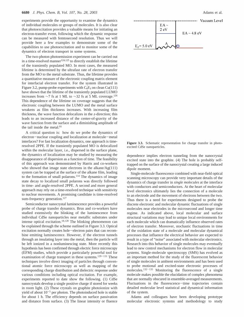
experiments provide the opportunity to examine the dynamicsof individual molecules or groups of molecules. It is also clearthat photoexcitation provides a valuable means for initiating anelectron-transfer event, following which the dynamic responsecan be measured with femtosecond resolution. Thus we willprovide here a few examples to demonstrate some of thecapabilities to use photoexcitation and to monitor some of thedynamics of electron transport in some systems.
The two-photon photoemission experiment can be carried outin a time-resolved manner124,125to directly establish the lifetimeof the transiently populated MO. In most cases, the measuredlifetime is determined by the ultrafast rate of electron transferfrom the MO to the metal substrate. Thus, the lifetime providesa quantitative measure of the electronic coupling matrix elementfor interfacial electron transfer. For the system illustrated inFigure 3.2, pump-probe experiments with C6F6 on clean Cu(111)have shown that the lifetime of the transiently populated LUMOincreases from∼7 fs at 1 ML to∼32 fs at 5 ML coverage.126
This dependence of the lifetime on coverage suggests that theelectronic coupling between the LUMO and the metal surfaceweakens as film thickness increases. With increasing filmthickness, the wave function delocalizes in thez-direction; thisleads to an increased distance of the center-of-gravity of thewave function from the surface and a diminishing amplitude ofthe tail inside the metal.81
A critical question is: how do we probe the dynamics ofelectron-nuclear coupling and localization at molecule-metalinterfaces? For fast localization dynamics, one approach is time-resolved 2PPE. If the transiently populated MO is delocalizedwithin the molecular layer, i.e., dispersed in the surface plane,the dynamics of localization may be studied by measuring thedisappearance of dispersion as a function of time. The feasibilityof this approach was demonstrated by Harris and co-workerswho showed that image state electrons in the alkane/Ag(111)system can be trapped at the surface of the alkane film, leadingto the formation of small polarons.114 The dynamics of imagestate decay to localized small polarons was directly followedin time- and angle-resolved 2PPE. A second and more generalapproach may rely on a time-resolved technique with sensitivityto nuclear movements. A promising candidate is time-resolvedsum-frequency generation.127
Semiconductor nanocrystal luminescence provides a powerfulprobe of charge transfer dynamics. Brus and co-workers havestudied extensively the blinking of the luminescence fromindividual CdSe nanoparticles near metallic substrates underintense optical excitation.18,128 The blinking phenomenon canbe explained through the scheme outlined in Figure 3.3. Opticalexcitation normally creates hole-electron pairs that can recom-bine emitting luminescence. However, if the electron tunnelsthrough an insulating layer into the metal, then the particle willbe left ionized in a nonluminescing state. More recently thishypothesis has been confirmed through electric force microscopy(EFM) studies, which provide a particularly powerful tool forexamination of charge transport in these systems.129-131 Thesetechniques involve direct imaging of particles through conven-tional atomic force microscopy as well as mapping of thecorresponding charge distribution and dielectric response undervarious conditions including optical excitation. For example,experiments reported to date show the following. (1) CdSenanocrystals develop a single positive charge if stored for weeksin room light. (2) These crystals on graphite photoionize withyield of about 10-5 per photon. The photoinduced hole is stablefor about 1 h. The efficiency depends on surface passivationand distance from surface. (3) The linear intensity or fluence
dependence implies electron tunneling from the nanocrystalexcited state into the graphite. (4) The hole is probably self-trapped on the surface of the nanocrystal creating a large induceddipole moment.
Single-molecule fluorescence combined with near-field opticalscanning microscopy can provide very important details of thedynamics of charge transfer insingle moleculesat the interfacewith conductors and semiconductors. At the heart of molecularlevel electronics ultimately lies the connection of a moleculeto an electrode and the movement of electrons between the two.Thus there is a need for experiments designed to probe thediscrete electronic and molecular dynamic fluctuations of singlemolecules near electrodes in the microsecond and longer timeregime. As indicated above, local molecular and surfacestructural variations may lead to unique local environments foreach molecule which can dramatically influence observed ratesof electron transfer. Moreover, stochastic fluctuations in timeof the oxidation state of a molecule and molecular dynamicalprocesses that influence the electrical behavior are expected toresult in a type of “noise” associated with molecular electronics.Research into this behavior of single molecules may eventuallylead to new control mechanisms for electron flow in molecularsystems. Single-molecule spectroscopy (SMS) has evolved asan important method for the study of the fluorescent behaviorof single molecules in ambient environments and has been usedto probe motional and excited-state electronic processes ofmolecules.132-135 Monitoring the fluorescence of a singlemolecule makes possible the elucidation of complex phenomenathat are normally obscured in ensemble-averaged measurements.Fluctuations in the fluorescence-time trajectories containdetailed molecular level statistical and dynamical informationof the system.
Adams and colleagues have been developing prototypemolecular electronic systems and methodology to study
Figure 3.3. Schematic representation for charge transfer in photo-excited CdSe nanoparticles.
6680 J. Phys. Chem. B, Vol. 107, No. 28, 2003 Adams et al.

photoinduced interfacial ET between single molecules andelectrodes.136-138 They have built a combined near-field scan-ning optical microscope and scanning confocal microscope thatallows them to measure the electron-transfer rate, to determinethe orientation of a molecular dipole in three dimensions, andto adjust the electron-transfer driving force for by applicationof an electric field via the metal-coated near-field probe.Through this research it should be possible to relate for a singlemolecule the kinetics of interfacial electron transfer to distance,molecular structure and dynamics, and energetics.
For example, recent experiments have been directed atmeasuring the single-molecule electron transfer in a chromo-phore/linker/electrode system where a perylene chromophoreis covalently attached to a modifiable alkyl-carboxylic linker(C11 in this case) and self-assembled at low concentration inmonolayers onto semiconductive and conductive electrodes suchas indium tin oxide and gold, Figure 3.4A.137 This is done byrepetitively exciting one molecule and determining the distribu-tion of “on” and “off” times. Optical excitation of a singleperylene from the ground state (S0) at a rate (kexc) leads tocreation of an excited state (S1) which decays either radiativelyat a rate (kr) or by charge injection into the conduction band(or trap states) of the electrode (ket), Figure 3.4B. The electronreturns to the molecule at a rate for back electron transfer (kbet).The fluorescence of single molecules near electrodes in self-assembled monolayers display blinking behavior with charac-teristic millisecond off periods (Figure 3.4D). Since the moleculeis not fluorescent in the charge transfer state, these off periodsmay be ascribed to discrete electron-transfer events. Thefluorescence blinking is not seen for molecules on polymer-coated glass surfaces since these provide no acceptor states. Theelectron-transfer rates can thus be obtained from an analysis ofthe fluorescence time trajectory.kbet is straightforwardly relatedto the average off time (tOFF), while the average on time (tON)is related to the excitation ratekexc times the quantum yield forthe forward ET process (Φet) and can be used to estimateket:(tOFF)-1 ) kbet and (tON)-1 ) kexc ket/(kr + ket) ) kexc Φet. Formany molecules, single-exponential behavior is observed forboth forward and back ET processes. Typical fits of theexperimental data for forward and back processes are shown inFigure 3.4C. Also apparent in fluorescence traces are discretejumps in fluorescence intensity (Figure 3.4D) on a time scaleof seconds, which may be the result of molecular reorientation
dynamics where intensity changes arise from increased ordecreased absorption of the polarized laser light.
In these experiments, the single molecules at the electrodesserve as probes of how a molecule with discrete energy levelscouples to an electrode with a spatially varying continuum ofstates, an energetically varying density of states, and trap sites.It is not exactly clear whether single exponential behavior shouldbe expected for a single molecule ET. If a molecule can transferan electron to a continuum of states and possibly differentdistinct trap sites and with different rates, should the result besingle exponential? Can an electron escape into the continuum?Experiments of this sort are currently directed at using near fieldmethods with polarized light to follow molecular orientationand dynamics and using electric fields to modulate the drivingforce of ET. Eventually it should be possible to use this methodto study transistor type molecules in self-assembled monolayerswithout the need to connect to three electrodes. Application ofan electric field could gate the flow of electrons betweendifferent legs of a trigonal molecule probed by optical methods.
3.4. Summary and Conclusions.To understand the phe-nomena relating to charge transport at the interface of a moleculewith a metal or semiconductor, it is clearly critical to elucidatethe actual nuclear configuration of the molecule at the interface(which can deviate considerably from the molecular configu-ration in solution or in the gas phase) and to elucidate thecorresponding electronic configuration (at least in the Born-Oppenheimer approximation). It is also necessary to understandthe coupling of the molecule in its interfacial configuration tothe metal or semiconductor. On the basis of this characterization,theory and new experimental techniques can help us develop adetailed understanding for both the static and dynamic behaviorof charge transport at the interface. Several experimental toolshave been developed to help provide the needed characterization.These include scanning probe techniques such as STM and AFMalong with new capabilities such as EFM. They also includenew spectroscopies including, for example, photoemissionspectroscopy and, in particular, two photon photoemission(2PPE). These spectroscopic techniques have been demonstratedto provide a wealth of static and dynamic information. Inaddition, single-molecule or single-particle luminescence tech-niques are proving to be very valuable tools for direct explora-tion of charge-transfer phenomena. Extension of this explorationto nanoparticle-organic systems of the type discussed in section
Figure 3.4. Electron transport at pyrene compounds adsorbed onto conducting substrates. (A) Schematic diagram. (B) Energy level diagram. (C)Decay kinetics. (D) Blinking phenomena.
Review Article J. Phys. Chem. B, Vol. 107, No. 28, 20036681

5.2 will be important to utilization of assemblies for energyconversion. With our present capabilities it is possible to beginto explore the fundamentals for charge transport at interfacesfor selected systems. However, much additional work and newtools will be required to develop a comprehensive understandingfor this important field.
4. Toward Functioning Molecular Electronics
Interest in fabricating devices based on active molecularcomponents has been driven by both the fundamental interestin understanding how chemistry can be used to build functionat the molecular level and by the looming technologicalexpectation of the end of Moore’s law. Can molecules bedesigned and incorporated into device structures to obtain solid-state analogues of two-terminal diodes and memory devices andthree-terminal transistors? By what mechanisms will each ofthese devices operate? Each device must be stable, providinglittle shift in turn-on or threshold voltage with operation andtime, and from device-to-device the turn-on or threshold voltagemust be the same.
4.1. Recent Advances.Some recent advances toward theunderstanding of the electronic properties of molecules areoutlined below.
(1) Scanning tunneling spectroscopy measurements of aro-matic thiols incorporated into self-assembled monolayers ofalkanethiols on Au(111) show higher conductivity for moleculeshaving aromatic versus aliphatic chains.139
(2) Using a revolutionary “break junction” technique, theresistance of 1,4-benzenedithiol was measured to be severalMΩ,24 much larger than Landauer’s quantum of resistanceh/2e2
) 12.9 kΩ,71 possibly arising from either a mismatch betweenthe Fermi level of Au and the relevant molecular orbital of themolecule, or because of other effects such as Coulomb blockade.
(3) Molecules of 2′-amino-4-ethynylphenyl-4′-ethynylphenyl-2′-nitro-1-benezenthiolate self-assembled onto a Au bottomelectrode and then topped by low-temperature evaporation of aAu electrode exhibit negative differential resistance inI-Vcharacteristics.102 The same molecules between Au electrodesexhibit low and high-conductivity states, with an exponentialdecay of the high-conductivity state of 800 s at 260 K: thishas been interpreted as a molecular random access memorycell.140 While negative differential resistance and changes inconductivity are observed only in nitro-derivatized molecules,stochastic switching in the conductivity of a single to a fewmolecules of the same ethynylphenylene backbone derivatizedwith and without nitro and amine substituents have beenobserved in STM.103
(4) The Landauer quantum of resistance, 12.9 kΩ71 has beenmeasured at room temperature between a single-walled carbonnanotube, glued to a conducting AFM tip, and a pool of liquidHg.141
(5) Field-effect transistors having carbon nanotubes as thesemiconducting channel, fabricated by stretching nanotubesacross source and drain electrodes, show p-type conduction withgood switching behavior.142,143More recently, n-type semicon-ducting behavior in single-walled carbon nanotubes was dem-onstrated by either vacuum annealing or K-doping the nanotube;this enabled p- and n-type regions to be fabricated within a singlenanotube and the demonstration of an intramolecular voltageinverter with a gain of 1.6.144Single-electron transistor behavior,characterized by Coulomb blockade, was reported in single-walled carbon nanotubes by defining∼20 nm coherent segmentsby kinking the tube on either side with an AFM tip.145
(6) A Langmuir-Blodgett monolayer of a bistable [2]catenane, with a naphthalene group as one “station” andtetrathiafulvalene as the second “station”, and a tetracationiccatenane hexafluorophosphate salt traveling on it like a “train”on a closed track, were deposited on poly-silicon as oneelectrode and topped by a 5 nm Ti layer and a 100 nm Alelectrode. The current-voltage plot is asymmetric as a functionof bias (which moves the train on the track), and a successionof read-write cycles shows that the resistance changes stepwiseas the train(s) move from the lower-conductivity station(s) tothe higher-conductivity station(s).146
(7) Unimolecular rectification across a Langmuir-Blodgettmonolayer of hexadecylquinolinium tricyanoquinodimethanidewas first detected between Mg and Pt electrodes147,148and laterobserved between Al electrodes,100,149,150most recently evenbetween oxide-free Au electrodes,151,152to be a variant of theAviram-Ratner mechanism.153 The original proposal suggesteda D-Bσ-A molecule connecting an electron donor moiety toan electron acceptor moiety through an insulating saturated“sigma” bridge Bσ; the mechanism of action involves inelastictunneling through the molecule from its first electronic excited-state D+-Bσ-A- to the less polar ground state D0-Bσ-A0.153
The first confirmed rectifier was a ground-state zwitterion D+-Bπ-A-, connected by a twistedπ bridge and used inelastictunneling from the lower-polarity excited-state D0-Bσ-A0 tothe higher-polarity ground state.154
(8) Most recently, two new monolayer rectifiers have beenfound when sandwiched between gold electrodes.155,156The firstis a pyridinium salt, in which the rectification seems to be dueto back-charge transfer from the anion to the pyridinium ion.157
The second is dimethylaminophenylazafullerene, which has atremendous rectification ratio (as high as 20,000): here,however, the bulk of the forward current seems to be due tothe formation of stalagmites of gold, which do not pierce themonolayer totally, but, once formed, behave ohmically.156
4.2. An Alternative Approach Using Quantum CellularAutomata. Section 2.3.3 discusses how an electric fieldinfluences the distribution of charges within molecules exposedto the field. Field-induced charge movement within a properlydesigned molecule could be used for transmitting or processinginformation in a cellular automaton architecture. In the quantum-dot cellular automata (QCA) architecture,158 bit information isstored in the charge configuration of cells constructed fromquantum dots. Charges move within the cells in response toexternal inputs or the electrostatic influence of neighboring cells.The cell-cell electrostatic interaction means that contacts mustonly be made at the edges of an array of QCA cells, and thatno current need flow through the cells.
QCA has been experimentally demonstrated at 80 mK innearly a dozen devices,159 including QCA cells, wires, and logicelements (AND/OR gates), and a clocked memory cell. A powergain of 2.1 was measured for the last device.160 Recent effortshave focused on implementing QCA at the molecular size scale,in which case each “quantum dot” would consist of a singleredox center and the “tunneling junction” would be an organicor inorganic bridging group. Molecular QCA is predicted tofunction at room temperature, and many mixed-valence mol-ecules would be suitable as QCA cells.161
Recent ab initio calculations162 show that the electrostaticforces between adjacent molecules are strong enough to causesignificant charge transfer to occur. For example, the 1,4-diallylbutane radical cation is a model two-dot QCA cell. It possessestwo redox centers (the allyl groups) located 7 Å apart, separatedby a butane bridge, and has a single positive charge that can be
6682 J. Phys. Chem. B, Vol. 107, No. 28, 2003 Adams et al.

located on either allyl site. Figure 4.1 shows a setup where twoof these molecules are fixed adjacent to a single positive charge(the “driver”). When the driver moves over a distance of 7 Å,it causes the positive charge in the neighboring molecule toswitch from one allyl group to the other; this perturbation inturn causes the positive charge in the next molecule to switch.Note that the molecule farthest from the driver winds up withits positive charge at the same side of the molecule as the driver,showing that it responds to the electrostatic forces imposed bythe intervening molecule
4.3. Issues and Needs.In diodes, it is desirable to obtain ahigh rectification ratio, with little leakage current, and anaccessible and stable turn-on voltage. In memory devices, theissues are switching time, on/off ratio, stability, volatility, andthe turn-on/off voltage. In transistors, what is the speed (relatedboth to “effective carrier mobility,” if it can be defined) andthe channel length, the current modulation (aka on-off ratio),the threshold voltage, and its stability?
The speed of switching depends on the mechanisms drivingthe change in the state of the molecule, giving rise to themeasured change in resistance. Mechanisms based on mechan-ical motion, which for example are the mechanistic basis ofring motion in molecules such as rotaxanes and catenanes, areinherently slow. Solution-phase NMR measurements of ringmotions in solution are∼500 times per second.163These motionsmay also be constrained by other molecules or interfaces in thesolid state. Mechanisms based on molecular diffusion orrequiring ionic diffusion should lead to microsecond switching
times typical of diffusion. The larger the molecule/ion and thelonger the distances it is required to move will limit the timescale for switching. Moving protons over short distances,∼3Å, has been proposed for switching and may provide the fastestobtainable switching speed for a system based on diffusion.164
Reduction-oxidation and conformational molecular changesmay provide the fastest (∼picosecond) time scales for switching.If, for example, reduction-oxidation is stabilized by thepresence of ions, the time scale for switching will depend onthe concentration and diffusion of ions, presumably limitingswitching once again to microsecond time scales. There is atpresent a lively debate about whether each practical moleculardevice must be as fast as possible (thus necessitating electronicprocesses for the molecular states involved in the devicefunction) or if slower devices (involving translation or molecularconformation) are acceptable, because, in a massively parallelarchitecture (Teramac), redundant interconnects with a fault-finding algorithm165 may yield an acceptably fast computer.
As discussed in section 2.3.3, intentional or unintentionalincorporation of ions may dramatically change the devicebehavior. If ions stabilize reduction-oxidation, removing theions may change both the time scale for switching and thevoltage for switching (which may or may not still be accessible).Environmental effects (ions, stray charges within a molecularlayer or at an interface) may create electric fields that shift turn-on/threshold voltages in molecular devices.
4.3.1. Intrinsic Limits to Molecular Electronics.The Bohrradius of an electron is 0.1 to 1.0 nm in “insulating” media.Because electrons will tunnel between wires spaced less than afew nm apart, “nanoelectronics” is the limit for circuits withelectrons as charge carriers. Since electron tunneling cannot beavoided, we should exploit differential electron tunneling innanoelectronics. A design for a nanotransistor that exploitsthis approach could connect source and drain electrodes throughan oligophenylene bridge containing ferrocene as a moleculargate. The effective electron tunneling distance depends onthe structure of the bridge; it is large for the aromatic unit(1/â ) 2.0 to 2.5 Å) and quite small for saturated (alkane)bridges (â ) 0.7 to 1.1 Å). How rapidly could such a gateswitch? If the electronic coupling (and thus level broadening)is limited to the order ofkT, the tunneling rate will be of theorder 2πkB(300 K)/h ) (25 fs)-1. Such a rate would allow1 THz gates if the circuit capacitances are sufficiently small.
The achievable density of molecular devices in a largerarchitecture will also be limited at the nanoscale by unavoidableelectronic tunneling as it may give rise to crosstalk betweendiscrete devices. While the field is still focused on understand-ing discrete molecular devices, at some point the need mayarise to develop synthetic routes to insulate devices and limitcrosstalk and to develop electronic schemes to take advantageof differential conductance and bistability in molecular struc-tures.
4.3.2. Energy Dissipation in Nanostructures.Perhaps the mostfrequently heard objection to single-molecule electronics is“won’t the current densities roast the molecule.” The objectionis based on an extrapolation of macroscale resistance to thenanoscale. This extrapolation is not valid. Once the size of astructure falls below the electron mean-free-path (severalhundred Å at room temperature), normal scattering processesno longer play a role. The electron moves from one point toanother (taking a semiclassical view) with a velocity given bydE/dk (of course, if there is no delocalization, dE/dk ) 0!). Inthis picture there is no scattering and so there is no classical,ohmic resistance and no power dissipation. Resistance (in the
Figure 4.1. Two molecules of 1,4-diallylbutane radical cation, fixed7 Å apart, and driven by a single positive charge that slides along thepath indicated by the black arrow. The driver is at the bottom of itspath at left and at the top at right. Gaussian 98 calculation usingHartree-Fock theory and the STO-3G basis set. (a) Quadrupole momentas a function of driver polarization; switching is nonlinear and stronglybistable. (b) Orbital isosurface (LUMO shown) at extremes of driverposition. (c) Isopotential surface (red indicates positive charge) atextremes of driver position.
Review Article J. Phys. Chem. B, Vol. 107, No. 28, 20036683

sense that current in a given field is not infinite) arises purelyfrom a transmission coefficient through the nanostructure thatis less than unity, i.e.,R ) h/2e2|T| (eq 2.11), a form of thewell-known Landauer equation. For a metallic nanojunctionwhere the metal atomic states in the junction are degeneratewith the bulk, |T| ) 1 and R ) 12.9 kΩ. In contrast, insmall alkanes, where states are far from the metallic Fermi level,R ∼ 109 Ω. This does not mean that the power dissipated inthe junction isV2/109 Ω! Rather, only one electron in 105 getsthrough the junction. Currents of up toµA have been measuredin junctions containing one or a few molecules with no long-term degradation of the junctions. The important factors are theapplied bias and the presence of electroactive contamination,both of which lead to irreversible electrochemical degradationof the molecule. An intriguing question remains in the case ofa nanoscale system containing redox centers. These trap ordonate charge because of coupling to nuclear motions. This isclearly a more complex situation than described by the Landauerapproach.
4.3.3. The Right Molecules/Materials.One may imagine anall-organic computer, with molecular electronic devices con-nected by, for example, a suitable organic conducting polymer“backplane”. However, at present, the lack of enough sturdyand fast molecular electronic devices suggests that for theforeseeable future, inorganic metal contacts will be used toaccess these devices. To the degree that such contacts remainimportant, there is a need for improved characterization andunderstanding of the thermodynamics, kinetics, and electronicproperties of the contact (see section 3) and for improvedchemical stability. Binding to a metal may simply result fromvan der Waals forces (as in Langmuir-Blodgett films) orthrough dative (e.g., NH3) or covalent bonding. Despite theformation of a strong covalent bond when a thiol binds a goldsubstrate, the resulting thiolates on Au can be oxidized tosulfoxides with time, creating local Schottky barriers withattendant band bending. In addition, gold atoms are quite mobile,and can move within the monolayer at certain (sufficient?)potentials.151
At present the scientific community has reported examplesof molecular “wires”, switches, and rectifiers. The yields of thesedevices are typically only∼1%, and reliable assembly ofmolecules and deposition of electrodes is required in the nearterm, to gain understanding of the behavior of molecular devices,and in the long term, for practical application of moleculardevices.
Most recent measurements (except for (5) above) have beenfor two-electrode systems. A crucial stumbling block formolecular electronics is that power gain (i.e., amplification) mustbe demonstrated in some device before the array of molecularelectronic components is considered to be sufficient for seriousassembly and circuit design. A great experimental challenge,at present under development by several laboratories simulta-neously, is the construction of three- or four-metal electrodes,or points, or shards, which are within 1 to 2 nm of each other.Approaches include complicated break junctions; burning nar-row interconnects by bursts of electrical power or by allowingstrands of conducting polymers to grow between slightly largergaps in metal electrodes, or using carbon nanotubes. When suchelectrode systems become available, then one can hope to thinkof bridging the gap between them by a novel single moleculewhose constituents are such that power gain is obtained fromsuch a device. Fabricating such electrodes and synthesizing the“right” molecule to direct its assembly within the gap areimportant challenges.
When is a contact ohmic? How does one make an ohmiccontact between an inorganic metal and an organic molecule?Making contact to molecules means contacting metal electrodeswithout damaging the molecule; an interesting new method isthe “cold gold” method.151,152At one extreme, if the metal probeis too far, then one has a tunneling gap, not an ohmic contact.At the other extreme, if the metal probe is too close, then themolecules must be compressed, and the energy levels of themolecules will be greatly modified by the contact. When themetal probe is at the “right” distance, then the series resistancebetween the metal electrode(s) and the molecule may be at aminimum. One might use nanopositioners (piezo drives) to findempirically when the contact resistance is minimized or whenthe resistance is small and there is no spectroscopic evidenceof damage to the molecule. Alternatively, the contact problemcan be addressed chemically, by incorporating into the moleculea functional group designed to bind the metal electrode asdiscussed above.
4.3.4. How Much Potential Can a Monolayer Withstand?The breakdown potential of dry air is about 30 000 V per cm,or 3× 10⁶ V/m. What is surprising is that potentials much largerthan this are experienced by molecules in scanning tunnelingmicroscope experiments (1 V/2 nm)) 5 × 10⁸ V/m. Mono-layers sandwiched between electrodes 2.5 nm apart of diameter0.2 to 0.5 mm2 can withstand between 2 V100 and even 5 V,151
which corresponds to a maximum of 2× 10⁹ V/m. Thisresistance to breakdown in monolayers is remarkable, butdeserves careful further study.
5. Architectures for Energy Conversion
Conversion and storage of solar energy requires efficientphoton capture, charge separation and transport, and, finally,efficient utilization or storage by chemical or electrochemicalmeans. The high surface area of nanostructures can immenselyenhance light-collection efficiency. Efficiencies of catalyticsequences used for utilization and storage are enhanced by thehigh surface area, as well. Thus there is the expectation thatnanoscale systems can advance solar photoconversion and thatadvances in the understanding of the relevant charge transfersand the strongly related energy transfersprocess to energyconversion will be central to this progress. As discussed insection 1, the nanostructures include molecular wires, nanopar-ticles, both of semiconductor and metal, nanotubes, electrodes,and the connectors that attach these objects to create largerstructures. Other motifs, such as filled zeolites, aerogels,dendrites, and layered polymers, also offer enormous potentialfor accomplishment of useful chemical functions. Some simpleassemblies are illustrated in Figure 5.1
This section addresses our current utilization and understand-ing of nanostructures and their complex assemblies in lightharvesting (5.1), light-induced charge transport (5.2), and chargestorage in advanced conductive aerogels (5.3).
5.1. Nanoscale Energy Transfer, Charge Transfer, andEnergy Conversion in Molecular Assemblies.During the past50 years, much has been learned about the factors that controlenergy transfer in molecular systems. The primary mechanismsfor energy transfer in molecular systems are Fo¨rster dipole-dipole coupling166 and Dexter exchange transfer.167
More recently the focus has turned to the study of energytransfer processes in supramolecular structures consisting ofcovalently or noncovalently bound assemblies of two or moreindividual molecular chromophores (Figure 5.2).168Much of thiswork has been inspired by the natural photosynthetic apparatusin which a large number of individual light-absorbing chro-
6684 J. Phys. Chem. B, Vol. 107, No. 28, 2003 Adams et al.
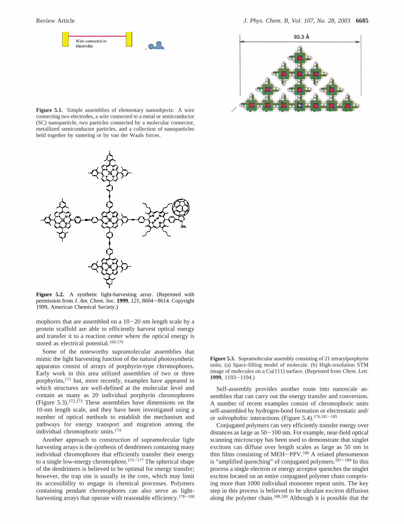
mophores that are assembled on a 10-20 nm length scale by aprotein scaffold are able to efficiently harvest optical energyand transfer it to a reaction center where the optical energy isstored as electrical potential.169,170
Some of the noteworthy supramolecular assemblies thatmimic the light harvesting function of the natural photosyntheticapparatus consist of arrays of porphyrin-type chromophores.Early work in this area utilized assemblies of two or threeporphyrins,171 but, more recently, examples have appeared inwhich structures are well-defined at the molecular level andcontain as many as 20 individual porphyrin chromophores(Figure 5.3).172,173 These assemblies have dimensions on the10-nm length scale, and they have been investigated using anumber of optical methods to establish the mechanism andpathways for energy transport and migration among theindividual chromophoric units.174
Another approach to construction of supramolecular lightharvesting arrays is the synthesis of dendrimers containing manyindividual chromophores that efficiently transfer their energyto a single low-energy chromophore.175-177 The spherical shapeof the dendrimers is believed to be optimal for energy transfer;however, the trap site is usually in the core, which may limitits accessibility to engage in chemical processes. Polymerscontaining pendant chromophores can also serve as light-harvesting arrays that operate with reasonable efficiency.178-180
Self-assembly provides another route into nanoscale as-semblies that can carry out the energy transfer and conversion.A number of recent examples consist of chromophoric unitsself-assembled by hydrogen-bond formation or electrostatic and/or solvophobic interactions (Figure 5.4).176,181-185
Conjugated polymers can very efficiently transfer energy overdistances as large as 50-100 nm. For example, near-field opticalscanning microscopy has been used to demonstrate that singletexcitons can diffuse over length scales as large as 50 nm inthin films consisting of MEH-PPV.186 A related phenomenonis “amplified quenching” of conjugated polymers.187-189 In thisprocess a single electron or energy acceptor quenches the singletexciton located on an entire conjugated polymer chain compris-ing more than 1000 individual monomer repeat units. The keystep in this process is believed to be ultrafast exciton diffusionalong the polymer chain.188,189Although it is possible that the
Figure 5.1. Simple assemblies of elementary nanoobjects: A wireconnecting two electrodes, a wire connected to a metal or semiconductor(SC) nanoparticle, two particles connected by a molecular connector,metallized semiconductor particles, and a collection of nanoparticlesheld together by sintering or by van der Waals forces.
Figure 5.2. A synthetic light-harvesting array. (Reprinted withpermission fromJ. Am. Chem. Soc.1999, 121, 8604-8614. Copyright1999, American Chemical Society.)
Figure 5.3. Supramolecular assembly consisting of 21 tetrarylporphyrinunits. (a) Space-filling model of molecule. (b) High-resolution STMimage of molecules on a Cu(111) surface. (Reprinted fromChem. Lett.1999, 1193-1194.)
Review Article J. Phys. Chem. B, Vol. 107, No. 28, 20036685
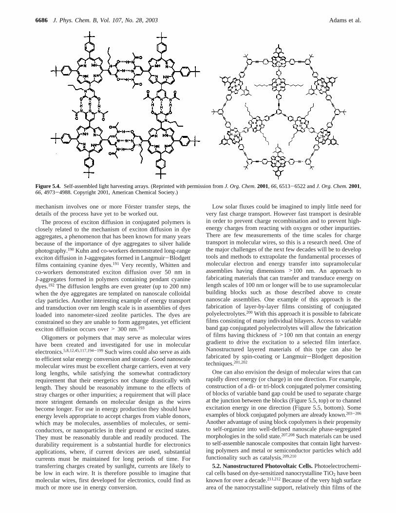
mechanism involves one or more Fo¨rster transfer steps, thedetails of the process have yet to be worked out.
The process of exciton diffusion in conjugated polymers isclosely related to the mechanism of exciton diffusion in dyeaggregates, a phenomenon that has been known for many yearsbecause of the importance of dye aggregates to silver halidephotography.190 Kuhn and co-workers demonstrated long-rangeexciton diffusion in J-aggregates formed in Langmuir-Blodgettfilms containing cyanine dyes.191 Very recently, Whitten andco-workers demonstrated exciton diffusion over 50 nm inJ-aggregates formed in polymers containing pendant cyaninedyes.192 The diffusion lengths are even greater (up to 200 nm)when the dye aggregates are templated on nanoscale colloidalclay particles. Another interesting example of energy transportand transduction over nm length scale is in assemblies of dyesloaded into nanometer-sized zeolite particles. The dyes areconstrained so they are unable to form aggregates, yet efficientexciton diffusion occurs over> 300 nm.193
Oligomers or polymers that may serve as molecular wireshave been created and investigated for use in molecularelectronics.5,8,12,45,117,194-199 Such wires could also serve as aidsto efficient solar energy conversion and storage. Good nanoscalemolecular wires must be excellent charge carriers, even at verylong lengths, while satisfying the somewhat contradictoryrequirement that their energetics not change drastically withlength. They should be reasonably immune to the effects ofstray charges or other impurities; a requirement that will placemore stringent demands on molecular design as the wiresbecome longer. For use in energy production they should haveenergy levels appropriate to accept charges from viable donors,which may be molecules, assemblies of molecules, or semi-conductors, or nanoparticles in their ground or excited states.They must be reasonably durable and readily produced. Thedurability requirement is a substantial hurdle for electronicsapplications, where, if current devices are used, substantialcurrents must be maintained for long periods of time. Fortransferring charges created by sunlight, currents are likely tobe low in each wire. It is therefore possible to imagine thatmolecular wires, first developed for electronics, could find asmuch or more use in energy conversion.
Low solar fluxes could be imagined to imply little need forvery fast charge transport. However fast transport is desirablein order to prevent charge recombination and to prevent high-energy charges from reacting with oxygen or other impurities.There are few measurements of the time scales for chargetransport in molecular wires, so this is a research need. One ofthe major challenges of the next few decades will be to developtools and methods to extrapolate the fundamental processes ofmolecular electron and energy transfer into supramolecularassemblies having dimensions>100 nm. An approach tofabricating materials that can transfer and transduce energy onlength scales of 100 nm or longer will be to use supramolecularbuilding blocks such as those described above to createnanoscale assemblies. One example of this approach is thefabrication of layer-by-layer films consisting of conjugatedpolyelectrolytes.200 With this approach it is possible to fabricatefilms consisting of many individual bilayers. Access to variableband gap conjugated polyelectrolytes will allow the fabricationof films having thickness of>100 nm that contain an energygradient to drive the excitation to a selected film interface.Nanostructured layered materials of this type can also befabricated by spin-coating or Langmuir-Blodgett depositiontechniques.201,202
One can also envision the design of molecular wires that canrapidly direct energy (or charge) in one direction. For example,construction of a di- or tri-block conjugated polymer consistingof blocks of variable band gap could be used to separate chargeat the junction between the blocks (Figure 5.5, top) or to channelexcitation energy in one direction (Figure 5.5, bottom). Someexamples of block conjugated polymers are already known.203-206
Another advantage of using block copolymers is their propensityto self-organize into well-defined nanoscale phase-segregatedmorphologies in the solid state.207,208Such materials can be usedto self-assemble nanoscale composites that contain light harvest-ing polymers and metal or semiconductor particles which addfunctionality such as catalysis.209,210
5.2. Nanostructured Photovoltaic Cells.Photoelectrochemi-cal cells based on dye-sensitized nanocrystalline TiO2 have beenknown for over a decade.211,212Because of the very high surfacearea of the nanocrystalline support, relatively thin films of the
Figure 5.4. Self-assembled light harvesting arrays. (Reprinted with permission fromJ. Org. Chem.2001, 66, 6513-6522 andJ. Org. Chem.2001,66, 4973-4988. Copyright 2001, American Chemical Society.)
6686 J. Phys. Chem. B, Vol. 107, No. 28, 2003 Adams et al.

dye sensitizer effectively harvest most of the incident light atwavelengths absorbed by the dyes. Much effort has beenexpended to optimize the efficiency of these cells and tounderstand the fundamental mechanisms for their operation.213
Solar-to-electrical energy conversion efficiencies approaching11% have been achieved. While there has been considerableenthusiasm for this technology, more work is required toincrease the efficiency of the dye-sensitized cells beforewidespread application becomes economical.
There has also been a substantial increase in the efficiencyof photovoltaic cells based on organic materials.214,215In mostcases, enhanced efficiencies have been achieved by creatingnanostructured heterojunctions, which result in interpenetrationof the donor and acceptor materials.216,217The nanoscale phase-segregated morphology overcomes a principal problem with theearlier devices based on “flat” heterojunctions, i.e., the largedistance that excitons must diffuse to arrive at the donor-acceptor junction. It is likely that further increases in theefficiency of organic photovoltaics will arise from the develop-ment of nanostructured materials that control the diffusion ofexcitons and charge carriers within the active material.
5.2.1. Inorganic-Organic Hybrid Structures for Light EnergyConVersion and Storage.Nanoscale materials are importantin developing a new generation of electronic and opticalnanodevices.75,218-222 Of particular interest are the semiconduc-tor and noble metal nanoclusters which display size-dependentoptical, electronic, and chemical properties (see for example,refs 18 and 223-231). It is a challenge for chemists to exploitthese unique properties in systems that carry out photochemicalconversion and storage of light energy. Despite the breakthroughrepresented by demonstration that nanostructured semiconduc-tor-based photochemical solar cells can operate with powerconversion efficiencies of 10-11%,213 barriers remain towardimproving the overall photoconversion efficiency. New strate-gies that exploit the architecture of metal-fluorophore nano-assemblies, as well as metal-semiconductor semiconductor-semiconductor composite structures, have to be designed toachieve efficient charge separation and transport of chargecarriers. The key to creation of these hybrid structures is tounderstand the chemistry at a fundamental level. Elucidationof the excited-state interactions with semiconductor and metalnanoparticles will continue to be a major research topic in thecoming years.
5.2.2. Interaction of Semiconductor and Metal Nanoparticleswith Organic Molecules.Assembling nanoparticles as spatiallywell-defined arrays is crucial in retaining the electronic proper-ties of individual particles. While it is beneficial to obtain robustarchitectures for light-harvesting applications, close packing ofmetal and semiconductor nanoparticles will cause aggregationeffects. For example, a red shift in the plasmon absorption isseen when metal nanoparticles undergo aggregation.232-235 Itshould be possible to maintain the spatial distance in 3-Dassemblies by binding these nanoparticles with suitable organicmolecules (e.g., alkane thiols). The distance separating theadjacent nanoparticles would then be determined by the lengthof the alkyl chain. If, on the other hand, photoactive moleculesare chemically bound to the semiconductor or metal surfacevia a functional end group such as-SH or-NR2, it can servethe dual purpose of spatial distribution as well as absorption ofincident photons. A layer-by-layer assembly of functionalizednanoparticles and redox couples can also provide the desiredarchitecture to obtain a 3-D array on an electrode surface.Significant efforts have been made to synthesize quantum dotsof semiconductor nanoparticles with narrow size distributions.Steigerwald et al.236,237 synthesized nanometer sized CdSeclusters using organometallic reagents in inverse micellarsolution followed by chemical modification of the surface ofthe clusters. Later the trioctylphosphine oxide (TOPO) method238
was developed to synthesize size-controlled CdSe nanocrystal-lites of the highest monodispersity (standard deviation less than5%). Capping CdSe colloids formed at high temperature (300°C) with TOPO stabilizes the particles against further growth.Capping with a large band gap semiconductor such as ZnSenhances the radiative recombination of photogenerated chargecarriers. Although this method has been widely adopted forsynthesis of quantum dots having narrow absorption andemission bands in the entire visible range, a simplified methodof preparing such colloids under ambient conditions remainsto be developed. The organic capping material usually controlsthe nature of surface states and hence excited-state dynamics.For particles of less than 2 nm, the majority of the atoms are atthe surface and so are in contact with the adjacent organic layer.
Although most published reports focus on the synthesisof organic capped gold nanoparticles, limited effort has beenmade to understand the mode of interaction of metal nano-particles with organic capping agents and solvents.239 Nuclearmagnetic resonance (NMR)240-244 and surface enhanced Ramanscattering (SERS),245,246as well as the spectroscopies describedin section 3, are useful techniques to probe the surface-inducedstructural distortion of the molecular geometry and nano-particle-molecule bonding sites and binding strength. Becauseof the photocatalytic activity of semiconductor colloids, one hasto look into the photostability issues of capping agents.247 A
Figure 5.5. Schematic diagram of a diblock copolymer comprisingconjugated polymer blocks of different band gap. CB and VB represent,respectively, the energy levels of the conduction and valence bands ofthe polymers. Arrows indicate the expected drift of photogeneratedelectrons (e-) and holes (h+). EET ) electronic energy transfer.
Figure 5.6. Examples of organic-capped semiconductor and metalnanoparticles.
Review Article J. Phys. Chem. B, Vol. 107, No. 28, 20036687
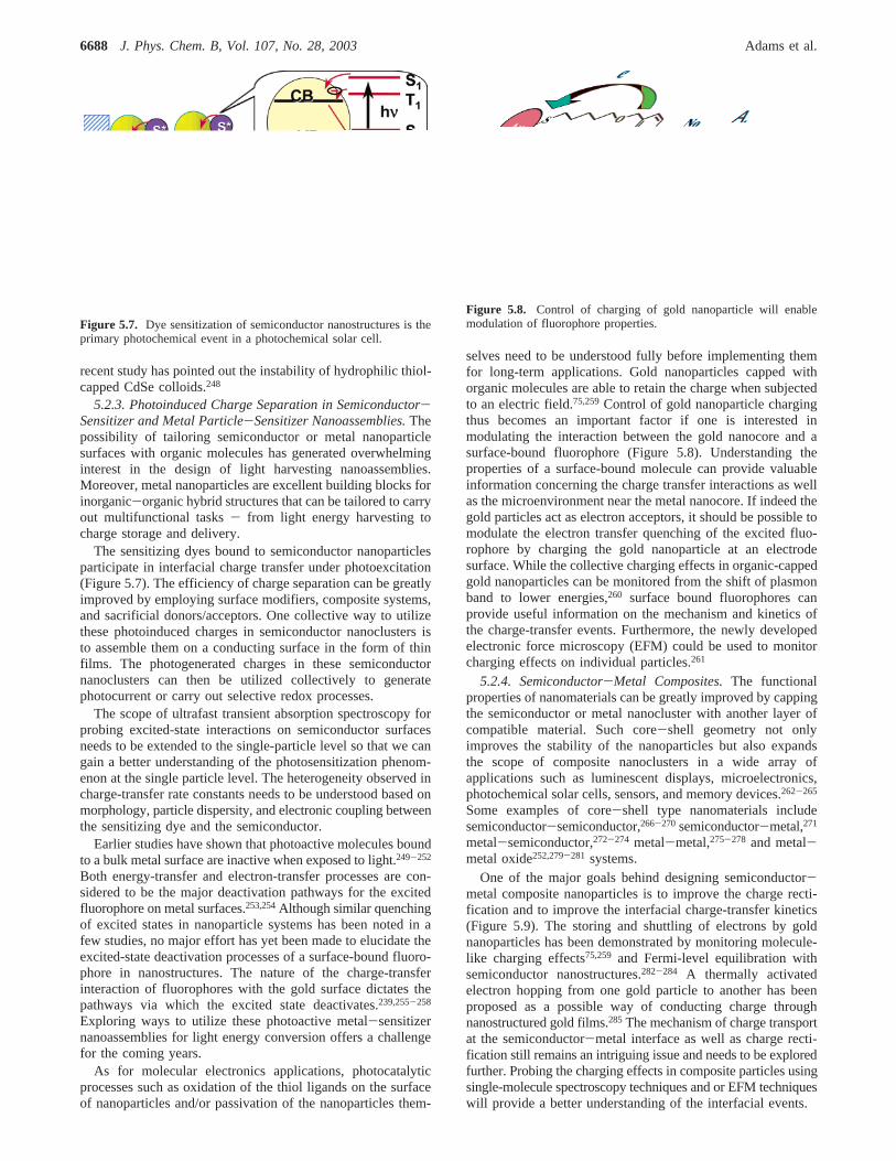
recent study has pointed out the instability of hydrophilic thiol-capped CdSe colloids.248
5.2.3. Photoinduced Charge Separation in Semiconductor-Sensitizer and Metal Particle-Sensitizer Nanoassemblies.Thepossibility of tailoring semiconductor or metal nanoparticlesurfaces with organic molecules has generated overwhelminginterest in the design of light harvesting nanoassemblies.Moreover, metal nanoparticles are excellent building blocks forinorganic-organic hybrid structures that can be tailored to carryout multifunctional tasks- from light energy harvesting tocharge storage and delivery.
The sensitizing dyes bound to semiconductor nanoparticlesparticipate in interfacial charge transfer under photoexcitation(Figure 5.7). The efficiency of charge separation can be greatlyimproved by employing surface modifiers, composite systems,and sacrificial donors/acceptors. One collective way to utilizethese photoinduced charges in semiconductor nanoclusters isto assemble them on a conducting surface in the form of thinfilms. The photogenerated charges in these semiconductornanoclusters can then be utilized collectively to generatephotocurrent or carry out selective redox processes.
The scope of ultrafast transient absorption spectroscopy forprobing excited-state interactions on semiconductor surfacesneeds to be extended to the single-particle level so that we cangain a better understanding of the photosensitization phenom-enon at the single particle level. The heterogeneity observed incharge-transfer rate constants needs to be understood based onmorphology, particle dispersity, and electronic coupling betweenthe sensitizing dye and the semiconductor.
Earlier studies have shown that photoactive molecules boundto a bulk metal surface are inactive when exposed to light.249-252
Both energy-transfer and electron-transfer processes are con-sidered to be the major deactivation pathways for the excitedfluorophore on metal surfaces.253,254Although similar quenchingof excited states in nanoparticle systems has been noted in afew studies, no major effort has yet been made to elucidate theexcited-state deactivation processes of a surface-bound fluoro-phore in nanostructures. The nature of the charge-transferinteraction of fluorophores with the gold surface dictates thepathways via which the excited state deactivates.239,255-258
Exploring ways to utilize these photoactive metal-sensitizernanoassemblies for light energy conversion offers a challengefor the coming years.
As for molecular electronics applications, photocatalyticprocesses such as oxidation of the thiol ligands on the surfaceof nanoparticles and/or passivation of the nanoparticles them-
selves need to be understood fully before implementing themfor long-term applications. Gold nanoparticles capped withorganic molecules are able to retain the charge when subjectedto an electric field.75,259Control of gold nanoparticle chargingthus becomes an important factor if one is interested inmodulating the interaction between the gold nanocore and asurface-bound fluorophore (Figure 5.8). Understanding theproperties of a surface-bound molecule can provide valuableinformation concerning the charge transfer interactions as wellas the microenvironment near the metal nanocore. If indeed thegold particles act as electron acceptors, it should be possible tomodulate the electron transfer quenching of the excited fluo-rophore by charging the gold nanoparticle at an electrodesurface. While the collective charging effects in organic-cappedgold nanoparticles can be monitored from the shift of plasmonband to lower energies,260 surface bound fluorophores canprovide useful information on the mechanism and kinetics ofthe charge-transfer events. Furthermore, the newly developedelectronic force microscopy (EFM) could be used to monitorcharging effects on individual particles.261
5.2.4. Semiconductor-Metal Composites.The functionalproperties of nanomaterials can be greatly improved by cappingthe semiconductor or metal nanocluster with another layer ofcompatible material. Such core-shell geometry not onlyimproves the stability of the nanoparticles but also expandsthe scope of composite nanoclusters in a wide array ofapplications such as luminescent displays, microelectronics,photochemical solar cells, sensors, and memory devices.262-265
Some examples of core-shell type nanomaterials includesemiconductor-semiconductor,266-270semiconductor-metal,271
metal-semiconductor,272-274 metal-metal,275-278 and metal-metal oxide252,279-281 systems.
One of the major goals behind designing semiconductor-metal composite nanoparticles is to improve the charge recti-fication and to improve the interfacial charge-transfer kinetics(Figure 5.9). The storing and shuttling of electrons by goldnanoparticles has been demonstrated by monitoring molecule-like charging effects75,259 and Fermi-level equilibration withsemiconductor nanostructures.282-284 A thermally activatedelectron hopping from one gold particle to another has beenproposed as a possible way of conducting charge throughnanostructured gold films.285The mechanism of charge transportat the semiconductor-metal interface as well as charge recti-fication still remains an intriguing issue and needs to be exploredfurther. Probing the charging effects in composite particles usingsingle-molecule spectroscopy techniques and or EFM techniqueswill provide a better understanding of the interfacial events.
Figure 5.7. Dye sensitization of semiconductor nanostructures is theprimary photochemical event in a photochemical solar cell.
Figure 5.8. Control of charging of gold nanoparticle will enablemodulation of fluorophore properties.
6688 J. Phys. Chem. B, Vol. 107, No. 28, 2003 Adams et al.

Semiconductor-metal nanocomposite particles have beenfound useful in improving the efficiency of photocatalytic andphotoelectrochemical conversion of light energy (see, forexample, ref 284 and references therein). Photogenerated holesin semiconductor materials such as TiO2 are strong oxidantsand are capable of oxidizing metals such as Au at thesemiconductor interface. Such oxidation events in compositefilms will not only disrupt the TiO2-metal interface but willalso create new electron-hole recombination centers. Thecontribution of these recombination centers is likely to becounterproductive for photoelectrochemical and photocatalyticoperation. Questions remain regarding the identity of oxidizedmetal ions and their role in altering the energetics of thesemiconductor. EXAFS studies can provide insight into theneighboring atoms as well as the oxidation state of theintercalated metal ions. Whereas modification of the semicon-ductor surface with metal nanoparticles promotes interfacialcharge transfer, it is important to tackle the problems associatedwith metal oxidation at the semiconductor-metal interface.
5.2.5. Light HarVesting Nanoassemblies.Exploring ways toimprove photoinduced charge separation in donor-acceptor typedyads and triads by binding them to metal nanostructures and/or semiconductor composites will aid in mimicking artificialphotosynthesis with improved efficiency. Fundamental under-standing of the dynamics and kinetics of the electron-transferprocess will allow us to optimize design strategies for such units.The basic role of the gold nanoparticle will be to promote chargeseparation and shuttle photogenerated electrons from a fluoro-phore or from a donor-acceptor dyad assembly to a collectingsurface. Based on a similar concept, efforts have recently beenmade to fabricate devices using a fluorescein photoreceptor onan Au/TiO2/Ti multilayer structure.286
By anchoring a redox moiety along with the fluorophoremolecule, it should be possible to achieve photoinduced chargeseparation in these molecular-metal nanoparticle assemblies(Figure 5.10). Anchoring a donor-acceptor dyad (e.g., C60-aniline dyad or Ru(bpy)3
2+-viologen dyad with a-SHfunctional group) on the gold surface can further advance theconcept of achieving charge separation in these photoactivenanoassemblies. The fullerene-aniline dyad in Figure 5.10illustrates the principle of this concept. This dyad has beenshown to undergo efficient charge separation and to producephotocurrent in a photoelectrochemical cell.287 By choosing aproper linker group it should be possible to systematically
investigate the distance dependent electron/energy transferprocesses between the metal nanoparticle and fluorophore.
5.3. Designing Three-Dimensional Pore-Solid Architec-tures as Advanced Electrochemical Materials for ChargeStorage and Energy Conversion.Disordered and amorphousmaterials are critical components in numerous technologies ofsocietal and military importance. Examples of such materials,in which charge transport is required for the technological enduse, include amorphous semiconductors (for photovoltaics orelectrophotographic imaging); superconducting cuprates andmagnetoresistive manganates whose properties derive fromlocalized defects (for motors and ferroelectrics, respectively);and insertion solids such as carbon and metal oxides or -hydrides(for electrochemical power storage).288 In particular, it hasrecently been recognized that nanoscale, poorly crystalline,charge-insertion solids function as high-performance materialsin power sources289 such as lithium-ion batteries,290-295 directmethanol fuel cells (DMFCs),296 and reformate-fed fuelcells.297-299 The difficulty of analytical and physicochemicalcharacterization of disordered-to-amorphous materials is furthercompounded when the materials and phases are nanoscopic.
5.3.1. Importance of Irregular/Nonperiodic Architectures.Asan example of the pervasiveness of the disordered realm,surfaces are actually nanoscale, often highly disordered, domainsthat differ from the underlying bulk and dictate many of thetechnologically most relevant catalytic, optical, or electricalproperties of the solid. In that the electrified interface mediatesthe properties and performance of all electrochemical powersources, understanding the nature of the surface, dependentlyand independently of bulk properties, has been a long-pursuedgoal of electrochemical surface science.300 Because our experi-mental bias lies toward synthesizing and characterizing orderedmaterials, the physical and chemical nature of the mosttechnologically relevant states are often poorly understood,especially when they are present only at a surface, under as-used conditions, or as nanoscale nonorder amidst orderedbulk.288,301
Conventional X-ray diffraction, and other traditional tech-niques used to determine the structure of materials, may be theplace to start when characterizing any new material, but it isnot the place to finish when working with charge-insertionnanomaterials of interest in batteries, supercapacitors, ultra-capacitors, electrochromics, photovoltaics, fuel cells, and elec-trocatalysis. Even with averaging spectroscopic techniques,
Figure 5.9. Interfacial charge-transfer processes in a metal-semiconductor nanoparticle.
Figure 5.10. Assembling nanoparticles and molecules for lightharvesting applications. Au-fullerene-aniline dyad assembly (bottom)illustrates the principle of photoinduced electron transfer and collectionof electrons at gold nanocore.
Review Article J. Phys. Chem. B, Vol. 107, No. 28, 20036689

which are thought to provide reliable information on nanoma-terials because such materials and objects have a large surface-to-volume ratio (a 2-nm Au particle has 63% of its atoms onthe surface), evidence is accumulating that interior vs. interface/surface still matters for nanomaterials.302-304
As an example of the need to understand heterogeneity anddisorder even in nanometer-scale solids, Scheme 1 illustrates aspectrum of properties for RuO2 as disorder creeps into order.Single-crystal RuO2 is a metallic conductor with a conductivityapproaching 105 S/cm.305 The anhydrous, polycrystalline formretains good electronic conductivity (∼102 S/cm) and finds usein thick-film resistors and as thin-film barrier layers to preventoxygen diffusion between silicon and the ferroelectric oxide inDRAM capacitors.306,307When the surface of RuO2 polycrys-talline films is made defective and becomes hydrous, theelectronic properties remain dominated by the polycrystallinebulk, but the surface becomes catalytically active and can storeelectron and proton charge in the damaged surface layer.308 Lowtemperature, sol-gel preparations produce bulk, highly disor-dered hydrous ruthenium oxide (RuO2‚xH2O or RuOxHy), whichstores electron and proton charge as a (nonlinear) function ofthe amount of structural water; an optimal storage of 720 F/g(F, capacitance) occurs for RuO2‚0.5 H2O (high-surface-areacarbon supercapacitors store<100 F/g309). When platinized,RuOxHy has recently been shown to be a more active catalyticstate for direct methanol oxidation than the current best DMFCcatalyst PtRu bimetallic alloy.296,310
As Scheme 1 indicates, when charge transport in a metaloxide is predominantly electronic (i.e., the charge carrier is anelectron) rather than electrical in nature (i.e., mixed electronplus ion or ion-only transport), the critical structure-propertypredictor is crystalline structure;and the absence of disorder.For RuO2, catalytic and charge/energy storage properties areenhanced when proton conductivity arises and the physico-chemical disorder at the surface or in the bulk increases. Metallicconductivity in hydrous ruthenium oxide persists even whenlong-range order, as determined by conventional X-ray diffrac-tion, is absent (even to compositions of RuO2‚xH2O, wherex g 2). When high-surface area RuO2‚∼2H2O (>50 m2/g) isdehydrated by heating in air, diffraction lines characteristic ofthe rutile habit only appear once the mole fraction of H2O dropsto x ∼ 0.3, at which point the charge-storage capacity of thesolid drops from 720 F/g (x ) 0.5) to 530 F/g.311
The local structure of RuO2‚xH2O, as determined by EXAFS(extended X-ray absorption fine structure), indicates that thebond distances in the RuO6 octahedra of RuO2‚∼2H2O arehighly distorted from those that characterize the rutile structure
(see Figure 5.11a).312 But EXAFS is an averaging structuraltechnique, which can mask the true nature of this and othercharge-transport materials, even on the nanoscale. When amedium-range structural analysis is performed on this familyof materials, using atomic-pair density functional analysis ofhigh energy X-ray diffraction patterns, the reason for retentionof metallic conductivity (even in RuO2‚∼2H2O) becomesapparent: nanocrystalline RuO2 persists at a volume fractionsufficient for a percolation path for electrons.313,314In essence,RuO2‚xH2O innately forms a bifunctional nanocomposite (Figure5.11b) in which the types of carriers that transport charge aredetermined by the composition of the nanocomposite: anelectron nanocrystalline wire (which becomes the majorityvolume fraction as RuO2‚xH2O is dehydrated) is always present,while protons are transported only in the disordered hydrousphase. With the structure-property insight made possible bydetermining the medium-range structure of RuO2‚xH2O, thenature of mixed conduction in this technologically importantcharge-insertion oxide, and perhaps other charge-insertion oxidesand materials, offers a new design strategy to optimize theproperties of materials that are functionally, physically, andchemically heterogeneous, rather than compositionally andstructurally uniform.
Determining medium-range structure is critical to understand-ing properties of disordered materials, disordered componentswithin ordered materials, and disordered interfaces, but thecurrent state-of-the-art requires intensive instrumentation: (1)variable coherence or fluctuation microscopy;315,316(2) pulsed,inelastic, wide or small angle, anomalous diffraction andscattering techniques that use X-ray or neutron sources;317-320
and (3) high-field magnetic resonance spectroscopy.318,321
Pragmatic drawbacks to these approaches as routine structuredeterminants (unlike the manner in which conventional XRDis widely available and routine) include the likely prerequisiteof a regional instrumentation facility; high-energy (>20 keVsynchrotron-derived) X-rays; nonthermal neutrons; high-voltageelectron microscopes or high-field resonance spectrometers; theamount or form of sample necessary for the analysis (gramsworth of nanoparticles for some of the scattering and diffractionapproaches; transmissive films or powders for electron micros-copy); high vacuum for the microscopy approaches (which maynot serve to establish the innate nature of the nanomaterial);and the difficulty of data analysis because the structuralassignments are coupled to intricate modeling.
If disorder or amorphousness is a desired state for a functionalmaterial (or phase within it) in applications requiring chargetransport, the challenge then becomes how to maintain the
SCHEME 1: Ruthenium DioxidesAn Example of the Spectrum of Properties for One Metal Oxide as Disorder Creepsinto Order
6690 J. Phys. Chem. B, Vol. 107, No. 28, 2003 Adams et al.

desired local structure in the face of thermodynamic forcesinherent to the application. In technologies dependent on chargetransport, such driving forces would include the operatingtemperatures of a fuel cell; electron-volts (eV) of stored (andcycled) energy in a battery; and harvesting several eV ofphotonic energy in a solar cell. Conversely, the functionalmaterial may exhibit greater performance tolerance underoperating conditions because highly disordered materials havea manifold of physically possible but energetically similarstructures, rather than a unique structure.322
5.3.2. Importance of Nothing in Nanoarchitectures.Nothing-free volume-is important in many charge-transfer situationsbecause reacting species or solvating molecules or mobile ions(or all three) must be transported to and from the reaction site,whether that site is another molecule or an electrified interfaceor a fabricated nanoscopic feature. As the rules of chargetransport on the nanoscale are explored and discerned, optimizedcharge-transport performance on the nanoscale will be realizedby fabricating supramolecular hierarchies, nanostructured ma-terials, or nanoarchitectures for specific applications. A case isbeing made that the performance and rate of electrochemicalprocesses improve when the “nothing” (i.e., porosity) isincorporated at the design stage in order to integrate effectivepaths for mass transport to (and away from) the nanostructuredelectroactive material.295,323,324Examples of such preplannedpore-solid architectural design of electrochemical materials
include membrane-templated materials,325aerogels,290,295 andlyotropically templated metals and metal oxides.326 Schematicrepresentations of these architectures, which contain nanostruc-tured solid and 2-, 3-, or 1-dimensional nanostructured porosity,respectively, are shown in Figure 5.12.
When disorder and nanoarchitecture intersect, recent literatureindicates that charge-insertion stoichiometries, rates of charge-discharge, and electrochromic efficiencies are greater than thoseobtained for the crystalline, dense materials.327 The Li-to-V2O5
stoichiometry increases to>4 for sol-gel-derived V2O5‚xH2O,as processed to yield minimal collapse of the pore network(thereby forming an aerogel or ambigel), while dense, poly-crystalline V2O5 stores at most one Li per V2O5.291,292 Themechanism(s) by which the ultraporous V2O5‚xH2O nanoarchi-tectures store the extra charge are under discussion,290,295butthe number density and nature of the defects may play a criticalrole in the increased charge storage available with V2O5
aerogels.Recent evidence supports the role of lattice defects on Li-
ion capacity in even micrometer-sized crystallites of V2O5.Deliberate atmosphere/temperature treatments to induce aniondefects lowered the Li ion capacity (relative to the as-receivedV2O5 powder), while treatment to induce proton-stabilized cationdefects increased the Li-ion capacity by 23%.328 Changes inthe long-range order of either the anion-defective or the proton-stabilized, cation-defective V2O5 were not apparent by conven-
Figure 5.11. Structure and charge-transport properties of high-surface-area RuO2 and the magnitude of charge stored in the oxide (pseudocapacitance)are all correlated, but the structure modeled for RuO2‚xH2O once long-range order is lost depends on whether the spectroscopy is sensitive toaveraged local structure (a) or medium-range structure (b).
Review Article J. Phys. Chem. B, Vol. 107, No. 28, 20036691
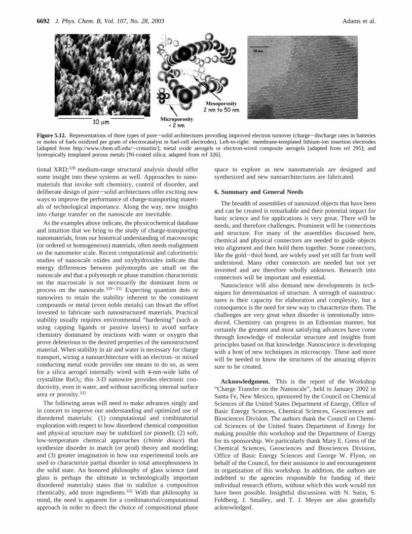
tional XRD;328 medium-range structural analysis should offersome insight into these systems as well. Approaches to nano-materials that invoke soft chemistry, control of disorder, anddeliberate design of pore-solid architectures offer exciting newways to improve the performance of charge-transporting materi-als of technological importance. Along the way, new insightsinto charge transfer on the nanoscale are inevitable.
As the examples above indicate, the physicochemical databaseand intuition that we bring to the study of charge-transportingnanomaterials, from our historical understanding of macroscopic(or ordered or homogeneous) materials, often needs realignmenton the nanometer scale. Recent computational and calorimetricstudies of nanoscale oxides and oxyhydroxides indicate thatenergy differences between polymorphs are small on thenanoscale and that a polymorph or phase transition characteristicon the macroscale is not necessarily the dominant form orprocess on the nanoscale.329-331 Expecting quantum dots ornanowires to retain the stability inherent to the constituentcompounds or metal (even noble metals) can thwart the effortinvested to fabricate such nanostructured materials. Practicalstability usually requires environmental “hardening” (such asusing capping ligands or passive layers) to avoid surfacechemistry dominated by reactions with water or oxygen thatprove deleterious to the desired properties of the nanostructuredmaterial. When stability in air and water is necessary for chargetransport, wiring a nanoarchitecture with an electron- or mixedconducting metal oxide provides one means to do so, as seenfor a silica aerogel internally wired with 4-nm-wide laths ofcrystalline RuO2; this 3-D nanowire provides electronic con-ductivity, even in water, and without sacrificing internal surfacearea or porosity.332
The following areas will need to make advances singly andin concert to improve our understanding and optimized use ofdisordered materials: (1) computational and combinatorialexploration with respect to how disordered chemical compositionand physical structure may be stabilized (or pinned); (2) soft,low-temperature chemical approaches (chimie douce) thatsynthesize disorder to match (or prod) theory and modeling;and (3) greater imagination in how our experimental tools areused to characterize partial disorder to total amorphousness inthe solid state. An honored philosophy of glass science (andglass is perhaps the ultimate in technologically importantdisordered materials) states that to stabilize a compositionchemically, add more ingredients.332 With that philosophy inmind, the need is apparent for a combinatorial/computationalapproach in order to direct the choice of compositional phase
space to explore as new nanomaterials are designed andsynthesized and new nanoarchitectures are fabricated.
6. Summary and General Needs
The breadth of assemblies of nanosized objects that have beenand can be created is remarkable and their potential impact forbasic science and for applications is very great. There will beneeds, and therefore challenges. Prominent will be connectionsand structure. For many of the assemblies discussed here,chemical and physical connectors are needed to guide objectsinto alignment and then hold them together. Some connectors,like the gold-thiol bond, are widely used yet still far from wellunderstood. Many other connectors are needed but not yetinvented and are therefore wholly unknown. Research intoconnectors will be important and essential.
Nanoscience will also demand new developments in tech-niques for determination of structure. A strength of nanostruc-tures is their capacity for elaboration and complexity, but aconsequence is the need for new way to characterize them. Thechallenges are very great when disorder is intentionally intro-duced. Chemistry can progress in an Edisonian manner, butcertainly the greatest and most satisfying advances have comethrough knowledge of molecular structure and insights fromprinciples based on that knowledge. Nanoscience is developingwith a host of new techniques in microscopy. These and morewill be needed to know the structures of the amazing objectssure to be created.
Acknowledgment. This is the report of the Workshop“Charge Transfer on the Nanoscale”, held in January 2002 inSanta Fe, New Mexico, sponsored by the Council on ChemicalSciences of the United States Department of Energy, Office ofBasic Energy Sciences, Chemical Sciences, Geosciences andBiosciences Division. The authors thank the Council on Chemi-cal Sciences of the United States Department of Energy formaking possible this workshop and the Department of Energyfor its sponsorship. We particularly thank Mary E. Gress of theChemical Sciences, Geosciences and Biosciences Division,Office of Basic Energy Sciences and George W. Flynn, onbehalf of the Council, for their assistance in and encouragementin organization of this workshop. In addition, the authors areindebted to the agencies responsible for funding of theirindividual research efforts, without which this work would nothave been possible. Insightful discussions with N. Sutin, S.Feldberg, J. Smalley, and T. J. Meyer are also gratefullyacknowledged.
Figure 5.12. Representations of three types of pore-solid architectures providing improved electron turnover (charge-discharge rates in batteriesor moles of fuels oxidized per gram of electrocatalyst in fuel-cell electrodes). Left-to-right: membrane-templated lithium-ion insertion electrodes[adapted from http://www.chem.ufl.edu/∼crmartin/]; metal oxide aerogels or electron-wired composite aerogels [adapted from ref 295]; andlyotropically templated porous metals [Ni-coated silica; adapted from ref 326].
6692 J. Phys. Chem. B, Vol. 107, No. 28, 2003 Adams et al.
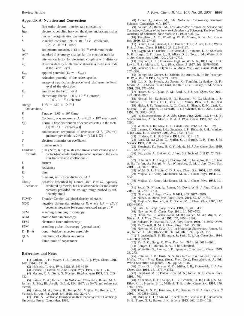
Appendix A. Notation and Conversions
ket first-order electron-transfer rate constant, s-1
HDA electronic coupling between the donor and acceptor sites
λ nuclear reorganization parameter
h Planck’s constant, 3.91× 10⁻¹⁵ eV-s/molecule,6.26× 10-34 J-s/mol
kB Boltzmann constant, 1.43× 10⁻²⁵ eV/K-molecule
∆G° standard free-energy change for the electron transfer
â attenuation factor for electronic coupling with distance
FM effective density of electronic states in a metal electrodeat the Fermi level
Eapp applied potential (EF ) -Eappe)
E° reduction potential of the redox species
ε energy of a particular electrode level relative to the Fermilevel of the electrode
EF energy of the Fermi level
e elementary charge 1.60× 10⁻¹⁹ C/proton;-1.60× 10-19 C/electron
energyconversions
1 eV ) 1.60× 10⁻¹⁹ J
F Faraday, 9.65× 10⁴ C/mol
C Coulomb, one ampere-s, A-s; 6.24× 10¹⁸ electrons/C
f(ε) Fermi-Dirac distribution of occupied states in the metalf(ε) ) 1/[1 + exp(ε/kBT)]
g conductance, reciprocal of resistanceΩ-1, (C2/J-s);quantum per mode is 2e2/h ) (12.8 k Ω)-1
T electron transmission coefficient
T transfer matrix
Landauerformula
g ) (2e2/h)T(EF); relates the linear conductanceg of acontact-(molecular bridge)-contact system to the elec-tron transmission coefficientT
I current
R resistance
Ω ohm
S Siemens, unit of conductance,Ω-1
Ohmicbehavior
behavior described by Ohm’s law:V ) IR, typicallyexhibited by metals, but also observable for molecularcontacts provided the voltage range probed is suf-ficiently small
FCWD Franck-Condon-weighted density of states
NDR negative differential resistanceR, where 1/R ) dI/dVbecomes negative for some restricted range of V
STM scanning tunneling microscopy
AFM atomic force microscopy
EFM electronic force microscopy
SPM scanning probe microscopy (general term)
D-B-A donor-bridge-acceptor assembly
QCA quantum dot cellular automata
F Farad, unit of capacitance
References and Notes
(1) Barbara, P. F.; Meyer, T. J.; Ratner, M. A.J. Phys. Chem.1996,100, 13148-13168.
(2) Holstein, T.Ann. Phys.1959, 8, 343-389.(3) Jortner, J.; Bixon, M.AdV. Chem. Phys.1999, 106, 1-734.(4) Marcus, R. A.; Sutin, N.Biochim. Biophys. Acta1985, 811, 265-
322.(5) Ratner, M. A.; Jortner, J. InMolecular Electronics; Ratner, M. A.,
Jortner, J., Eds.; Blackwell: Oxford, UK, 1997; pp 5-72 and referencestherein.
(6) Ratner, M. A.; Davis, B.; Kemp, M.; Mujica, V.; Roitberg, A.;Yaliraki, S. Ann. N.Y. Acad. Sci.1998, 852, 22-37.
(7) Datta, S.Electronic Transport in Mesoscopic Systems; CambridgeUniversity Press: Cambridge, 1995.
(8) Jortner, J., Ratner, M., Eds.Molecular Electronics; BlackwellScience: Cambridge, MA, 1997.
(9) Aviram, A., Ratner, M., Eds.Molecular Electronics: Science andTechnology(Annals of the New York Academy of Sciences); The New YorkAcademy of Sciences: New York, NY, 1998; Vol. 852.
(10) Templeton, A. C.; Wuelfing, W. P.; Murray, R. W.Acc. Chem.Res.2000, 33, 27-36.
(11) Bumm, L. A.; Arnold, J. J.; Dunbar, T. D.; Allara, D. L.; Weiss,P. S.J. Phys. Chem. B1999, 103, 8122-8127.
(12) Cygan, M. T.; Dunbar, T. D.; Arnold, J. J.; Bumm, L. A.; Shedlock,N. F.; Burgin, T. P.; Jones, L., II; Allara, D. L.; Tour, J. M.; Weiss, P. S.J. Am. Chem. Soc.1998, 120, 2721-2732.
(13) Claypool, C. L.; Francesco Faglioni, W. A. G., III; Gray, H. B.;Lewis, N. S.; Marcus, R. A.J. Phys. Chem. B1997, 101, 5978-5995.
(14) Giancarlo, L. C.; Flynn, G. W.Annu. ReV. Phys. Chem.1998, 49,297-336.
(15) Dorogi, M.; Gomez, J.; Osifchin, R.; Andres, R. P.; Reifenberger,R. Phys. ReV. B 1995, 52, 9071-9077.
(16) Cui, X. D.; Primak, A.; Zarate, X.; Tomfohr, J.; Sankey, O. F.;Moore, A. L.; Moore, T. A.; Gust, D.; Harris, G.; Lindsay, S. M.Science2001, 294, 571-574.
(17) Haram, S. K.; Quinn, B. M.; Bard, A. J.J. Am. Chem. Soc.2001,123, 8860-8861.
(18) Nirmal, M.; Dabbousi, B. O.; Bawendi, M. G.; Macklin, J. J.;Trautman, J. K.; Harris, T. D.; Brus, L. E.Nature 1996, 383, 802-804.
(19) Hicks, J. F.; Templeton, A. C.; Chen, S.; Sheran, K. M.; Jasti, R.;Murray, R. W.; Debord, J.; Schaaff, T. G.; Whetten, R. L.Anal. Chem.1999, 71, 3703-3711.
(20) (a) Stuchebrukhov, A. A.AdV. Chem. Phys.2001, 118, 1-44. (b)Stuchebrukhov, A. A.; Marcus, R. A.J. Phys. Chem.1995, 99, 7581-7590.
(21) Winkler, J. R.; Gray, H. B.Chem. ReV. 1992, 93, 369-379.(22) Langen, R.; Chang, I.-J.; Germanas, J. P.; Richards, J. H.; Winkler,
J. R.; Gray, H. B.Science1995, 269, 1733-1735.(23) Chidsey, C. E. D.Science1991, 251, 919-922.(24) Reed, M. A.; Zhou, C.; Muller, C. J.; Burgin, T. P.; Tour, J. M.
Science1997, 278, 252-254.(25) Slowinski, K.; Fong, H. K. Y.; Majda, M.J. Am. Chem. Soc.1999,
121, 7257-7261.(26) Bezryadin, A.; Dekker, C.J. Vac. Sci. Technol. B1997, 15, 793-
799.(27) Holmlin, R. E.; Haag, R.; Chabinyc, M. L.; Ismagilov, R. F.; Cohen,
A. E.; Terfort, A.; Rampi, M. A.; Whitesides, G. M.J. Am. Chem. Soc.2001, 123, 5075-5085.
(28) Wold, D. J.; Frisbie, C. D.J. Am. Chem. Soc.2000, 122, 2970.(29) Mujica, V.; Kemp, M.; Ratner, M. A.J. Chem. Phys.1994, 101,
6849.(30) Mujica, V.; Kemp, M.; Ratner, M. A.J. Chem. Phys.1994, 101,
6856.(31) Segal, D.; Nitzan, A.; Ratner, M.; Davis, W. B.J. Phys. Chem. B
2000, 104, 2790-2793.(32) Nitzan, A.J. Phys. Chem. B2001, 105, 2677-2679.(33) Nitzan, A.Annu. ReV. Phys. Chem.2002, 52, 681-750.(34) Mujica, V.; Roitberg, A. E.; Ratner, M.J. Chem. Phys.2000, 112,
6834-6839.(35) Sutin, N.Prog. Inorg. Chem.1983, 30, 441-498.(36) Newton, M. D.Chem. ReV. 1991, 91, 767-792.(37) Davis, W. B.; Wasielewski, M. R.; Ratner, M. A.; Mujica, V.;
Nitzan, A. J. Phys. Chem. A1997, 101, 6158-6164.(38) Siddarth, P.; Marcus, R. A.J. Phys. Chem.1990, 94, 2985-2989.(39) McConnell, H. M.J. Chem. Phys.1961, 35, 508.(40) Newton, M. D.; Cave, R. J. InMolecular Electronics; Ratner, M.
A., Jortner, J., Eds.; Blackwell: Oxford, UK, 1997; pp 73-118.(41) Brunschwig, B. S.; Ehrenson, S.; Sutin, N.J. Am. Chem. Soc.1984,
106, 6858-6859.(42) Yu, Z. G.; Song, X.Phys. ReV. Lett. 2001, 86, 6018-6021.(43) Renger, T.; Marcus, R. A., to be submitted.(44) Woitellier, S.; Launay, J. P.; Spangler, C. W.Inorg. Chem.1989,
28, 273.(45) Reimers, J. R.; Hush, N. S. InElectron Ion Transfer Condens.
Media: Theor. Phys. React. Kinet., Proc. Conf.; Kornyshev, A. A., Ed.;World Scientific: Singapore, 1997; pp 326-346.
(46) Closs, G. L.; Johnson, M. D.; Miller, J. R.; Piotrowiak, P.J. Am.Chem. Soc.1989, 111, 3751-3753.
(47) Shephard, M. J.; Paddon-Row, M. N.; Jordan, K. D.Chem. Phys.1993, 176.
(48) Yonemoto, E. H.; Saupe, G. B.; Schmehl, R. H.; Hubig, S. M.;Riley, R. L.; Iverson, B. L.; Mallouk, T. E.J. Am. Chem. Soc.1994, 116,4786-4795.
(49) Tong, G. S. M.; Kurnikov, I. V.; Beratan, D. N.J. Phys. Chem. B2002, 106, 2381-2392.
(50) Murphy, C. J.; Arkin, M. R.; Jenkins, Y.; Ghatlia, N. D.; Bossmann,S. H.; Turro, N. J.; Barton, J. K.Science1993, 262, 1025-1029.
Review Article J. Phys. Chem. B, Vol. 107, No. 28, 20036693

(51) Fukui, K.; Tanaka, K.Angew. Chem., Int. Ed. Engl.1998, 37, 158-161.
(52) Jortner, J.; Bixon, M.; Langenbacher, T.; Beyerle, M. E.; Langen-bacher, T.; Beyerle, M. E.Proc. Nat. Acad. Sci.1998, 95, 12759.
(53) Jortner, J.; Bixon, M.; Langenbacher, T.; Beyerle, M. E.Proc. Natl.Acad. Sci.1998, 95, 12759.
(54) Giese, B.; Amaudrut, J.; Ko¨hler, A.-K.; Spormann, M.; Wessely,S. Nature2001, 412, 318-320.
(55) Davis, W. B.; Svec, W. A.; Ratner, M. A.; Wasielewski, M. R.Nature1997, 396, 60.
(56) Davis, W. B.; Hess, S.; Naydenova, I.; Haselsberger, R.; Ogrodnik,A.; Newton, M. D.; Michel-Beyerle, M. E.J. Am. Chem. Soc.2002, 124,2422-2423.
(57) Levich, V. G. InAdVances in Electrochemistry and ElectrochemicalEngineering; Delahay, P., Tobias, C. W., Eds.; Interscience: New York,1966; Vol. 4.
(58) Royea, W. J.; Fajardo, A. M.; Lewis, N. S.J. Phys. Chem. B1997,105, 11152-11159.
(59) Gosavi, S.; Marcus, R. A.J. Phys. Chem. B2000, 104, 2067-2072.
(60) Smalley, J. F.; Feldberg, S. W.; Chidsey, C. E. D.; Linford, M. R.;Newton, M. D.; Liu, Y.-P.J. Phys. Chem.1995, 99, 13141.
(61) Gosavi, S.; Qin Gao, Y.; Marcus, R. A.J. Electroanal. Chem.2001,500, 71-77.
(62) Weber, K.; Hockett, L.; Creager, S.J. Phys. Chem. B1997, 101,8286.
(63) Sachs, S. B.; Dudeck, S. P.; Hsung, R. P.; Sita, S. R.; Smalley, J.F.; Newton, M. D.; Feldberg, S. W.; Chidsey, C. E. D.J. Am. Chem. Soc.1997, 119, 10563-10564.
(64) Sikes, H. D.; Smalley, J. F.; Dudek, S. P.; Cook, A. R.; Newton,M. D.; Chidsey, C. E. D.; Feldberg, S. W.Science2001, 291, 1519-1523.
(65) Creager, S.; Yu, C. J.; Bamdad, C.; O’Connor, S.; MacLean, T.;Lam, E.; Chong, Y.; Olsen, G. T.; Luo, J.; Gozin, M.; Kayyem, J. F.J.Am. Chem. Soc.1999, 121, 1059-1064.
(66) Smith, C. P.; White, H. S.Anal. Chem.1992, 64, 2398-2405.(67) Fawcett, W. R.J. Electroanal. Chem.1994, 378, 117-124.(68) (a) Vakarin, E. V.; Holovko, M. F.; Piotrowiak, P.Chem. Phys.
Lett. 2002, 363, 7-12. (b) Sumner, J. J.; Creager, S. E.J. Phys. Chem. B2001, 105, 8739-8745.
(69) Marcus, R. A.J. Phys. Chem. B1998, 102, 10071-10077.(70) Barnett, R. N.; Cleveland, C. L.; Joy, A.; Landman, U.; Schuster,
G. B. Science2001, 294, 567-571.(71) Landauer, R.IBM J. Res. DeV. 1957, 1, 223-231.(72) Kerqueris, C.; Bourgoin, J.-P.; Palacin, S.; Esteve, D.; Urbina, C.;
Magoga, M.; Joachim, C.Phys. ReV. B 1999, 59, 12505-12513.(73) Selzer, Y.; Salomon, A.; Cahen, D.J. Am. Chem. Soc.2002, 124,
2886-2887.(74) Brown, L. O.; Hutchison, J. E.J. Am. Chem. Soc.1997, 119, 9,
12384-12385.(75) Chen, S.; Ingram, R. S.; Hostetler, M. J.; Pietron, J. J.; Murray, R.
W.; Schaaff, T. G.; Khoury, J. T.; Alvarez, M. M.; Whetten, R. L.Science1998, 280, 2098-2101.
(76) Tomfohr, J. K.; Sankey, O. F.Phys. ReV. B 2002, 65, 245105-245112.
(77) Monch, W. On the physics of metal-semiconductor interfaces,Reports on Progress in Physics1990, 53, 221-278.
(78) Tersoff, J.Phys. ReV. Lett. 1984, 52, 465-468.(79) Xue, Y.; Datta, S.; Ratner, M. A.J. Chem. Phys.2001, 115, 4292-
4299.(80) Shen, C.; Kahn, A.; Hill, I. G. InConjugated Polymer and
Molecular Interfaces; Salaneck, W. R., Seki, K., Kahn, A., Pireaux, J. J.,Eds.; Marcel Dekker: New York, 2001; pp 351-400.
(81) Zhu, X. Y.Annu. ReV. Phys. Chem.2002, 53, 221-247.(82) Li, J.; Tomfohr, J. K.; Sankey, O. F. to be published.(83) Tian, W.; Datta, S.; Hong, S.; Reifenberger, R.; Henderson, J. I.;
Kubiak, C. P.J. Chem. Phys.1998, 109, 2874-2882.(84) Taylor, J.; Brandbyge, M.; Stokbro, K.Phys. ReV. Lett. 2002, 89,
138301-138301, 138304.(85) Segal, D.; Nitzan, A.; Davis, W. B.; Wasielewski, M. R.; Ratner,
M. A. J. Phys. Chem. B2000, 104, 3817-3829.(86) Yaliraki, S. N.; Roitberg, A. F.; Gonzalez, C.; Mujica, V.; Ratner,
M. A. J. Chem. Phys.1999, 111, 6997.(87) McConnell, H. M.J. Chem. Phys.508, 35, 508.(88) Sumner, J. J.; Creager, S. E.J. Am. Chem. Soc.2000, 122, 11914-
11920.(89) Lewis, N. S.J. Phys. Chem. B1998, 102, 4843-4855.(90) Economou, E. N.Green’s Functions in Quantum Physics; Springer-
Verlag: Berlin, 1983; Chapter 4.(91) Sumner, J. J.; Weber, K. S.; Hockett, L. A.; Creager, S. E.J. Phys.
Chem. B2000, 104, 7449.(92) Cui, X. D.; Primak, A.; Zarate, X.; Tomfohr, J.; Sankey, O. F.;
Moore, A. L.; Moore, T. A.; Gust, D.; Nagahara, L. A.; Lindsay, S. M.J.Phys. Chem.2002, 106, 8609-8614.
(93) Wold, D. J.; Haag, R.; Rampi, M. A.; Frisbie, C. D.J. Phys. Chem.B 2002, 106, 2813-2816.
(94) Hsu, C.-P.; Marcus, R. A.J. Chem. Phys.1997, 106, 584-598.(95) Fan, F.-R. F.; Yang, J.; Dirk, S. M.; Price, D. W.; Kosynkin, D.;
Tour, J. M.; Bard, A. J.J. Am. Chem. Soc.2001, 123, 2454-2455.(96) Murray, R. W., Ed.Molecular Design of Electrode Surfaces;
Techniques of Chemistry Series; John Wiley & Sons: New York, 1992;Vol. 22.
(97) Hicks, J. F.; Zamborini, F. P.; Osisek, A.; Murray, R. W.J. Am.Chem. Soc.2001, 123, 7048-7053.
(98) Feldheim, D. L.; Keating, C. D.Chem. Soc. ReV. 1998, 27, 1-12.(99) Sampaio, J. F.; Beverly, K. C.; Heath, J. R.J. Phys. Chem. B2001,
105, 8797-8800.(100) Metzger, R. M.; Chen, B.; Hopfner, U.; Lakshmikantham, M. V.;
Vuillaume, D.; Kawai, T.; Wu, X.; Tachibana, H.; Hughes, T. V.; Sakurai,H.; Baldwin, J. W.; Hosch, C.; Cava, M. P.; Brehmer, L.; Ashwell, G. J.J.Am. Chem. Soc.1997, 119, 10455-10466.
(101) Collier, C. P.; Wong, E. W.; Belohradsky´, M.; Raymo, F. M.;Stoddart, J. F.; Kuekes, P. J.; Williams, R. S.; Heath, J. R.Science1999,285, 391-394.
(102) Chen, J.; Reed, M. A.; Rawlett, A. M.; Tour, J. M.Science1999,286, 1550-1552.
(103) Donhauser, Z. J.; Mantooth, B. A.; Kelly, K. F.; Bumm, L. A.;Monnell, J. D.; Stapleton, J. J.; Price, D. W., Jr.; Rawlett, A. M.; Allara,D. L.; Tour, J. M.; Weiss, P. S.Science2001, 292, 2303-2307.
(104) Service, R. F.Science2001, 294, 2442-2443.(105) Pease, A. R.; Jeppesen, J. O.; Stoddart, J. F.; Luo, Y.; Collier, C.
P.; Heath, J. R.Acc. Chem. Res.2001, 34, 433-444.(106) Kagan, C. R.; Afzali, A.; Martel, R.; Gignac, L. M.; Solomon, P.
M.; Schrott, A. G.; Ek, B.Nano Lett.2003, 3, 119-124.(107) Lee, J.-O.; Lientschnig, G.; Wiertz, F.; Martin Struijk, R. A. J. J.;
Egberink, R.; Reinhoudt, D. N.; Hadley, P.; Dekker, C.Nano Lett.2003,3, 113-117.
(108) Scho¨n, J. H.; Meng, H.; Bao, Z.Nature2003, 422, 92.(109) Yaliraki, S. N.; Ratner, M. A.J. Chem. Phys.1998, 109, 5036.(110) Yaliraki, S. N.; Kemp, M.; Ratner, M. A.J. Am. Chem. Soc.1999,
121, 3428.(111) Newns, D. M.Phys. ReV. Lett. 1969, 178, 1123.(112) Anderson, P. W.Phys. ReV. Lett. 1961, 124, 41.(113) Lang, N. D.Phys. ReV. B 1995, 52, 5335.(114) Seminario, J. M.; Zacarias, A. G.; Tour, J. M.J. Am. Chem. Soc.
1999, 121, 411.(115) Magoga, M.; Joachim, C.Phys. ReV. B 1997, 56, 4722.(116) Stipe, B. C.; Rezaei, M. A.; Ho, W.Science1998, 280, 1732.(117) Hu, J.; Odom, T. W.; Lieber, C. M.Acc. Chem. Res.1999, 32,
435.(118) Avouris, Ph.J. Phys. Chem.1990, 94, 2246.(119) Dutton, G.; Zhu, X.-Y.J. Phys. Chem. B2001, 105, 10912.(120) Selzer, Y.; Salomon, A.; Cahen, D.J. Am. Chem. Soc.2002, 123.(121) Son, K. A.; Kim, H. I.; Houston, J. E.Phys. ReV. Lett.2001, 86,
5357.(122) Vondrak, T. W. H.; Winget, P.; Cramer, C. J.; Zhu, X.-Y.J. Am.
Chem. Soc.2000, 122, 4700-4707.(123) Miller, A. D.; Gaffney, K. J.; Liu, S. H.; Szymanski, P.; Garrett-
Roe, S.; Wong, C. M.; Harris, C. B.J. Phys. Chem. A2002, 106, 7636-7638.
(124) Petek, H.; Ogawa, S.Prog. Surf. Sci.1998, 56, 239.(125) Harris, C. B.; Ge, N.-H.; Lingle, R. L.; McNeill, J. D.; Wong, C.
M. Annu. ReV. Phys. Chem.1997, 48, 711.(126) Gahl, C.; Ishioka, K.; Zhong, Q.; Hotzel, A.; Wolf, M.Faraday
Discuss.2000, 117, 191.(127) Bonn, M.; Hess, C.; Wolf, M.J. Chem. Phys.2001, 115, 7725.(128) Nirmal, M.; Brus, L. E.Acc. Chem. Res.1999, 32, 407.(129) Krauss, T. D.; Brus, L. E.Phys. ReV. Lett. 1999, 83, 4840.(130) Krauss, T. D.; O’Brien, S.; Brus, L. E.J. Phys. Chem. B2001,
105, 1725-1733.(131) Cherniavskaya, O.; Chen, L.; Islam, M. A.; Brus, L.Nano Lett.
2003, 3, 497-501.(132) Xie, X. S.; Trautman, J. K.Annu. ReV. Phys. Chem.1998, 49,
441-480.(133) Van-Hulst, N. F.; Veerman, J. A.; Garcia-Parajo, M. F.; Kuipers,
L. J. Chem. Phys.2000, 112, 7799-7810.(134) Nie, S. M.; Zare, R. N.Ann. ReV. Biophys. Biomol. Struct.1997,
26, 567-596.(135) Moerner, W. E.J. Phys. Chem. B2002, 106, 910-927.(136) Zang, L.; Liu, R.; Holman, M. W.; Nguyen, K. T.; Adams, D. M.
J. Am. Chem. Soc.2002, 124, 10640-10641.(137) Holman, M. W.; Liu, R.; Zang, L.; Adams, D. M.J. Am. Chem.
Soc., submitted.(138) Liu, R.; Holman, M. W.; Zang, L.; Adams, D. M.J. Phys. Chem.
A, submitted.
6694 J. Phys. Chem. B, Vol. 107, No. 28, 2003 Adams et al.

(139) Bumm, L. A.; Arnold, J. J.; Cygan, M. T.; Dunbar, T. D.; Burgin,T. P.; Jones, L., II; Allara, D. L.; Tour, J. M.; Weiss, P. S.Science1996,271, 1705-1707.
(140) Reed, M. A.; Chen, J.; Rawlett, A. M.; Price, D. W.; Tour, J. M.Appl. Phys. Lett.2001, 78, 3735-3737.
(141) Frank, S.; Poncharal, P.; Wang, Z. L.; de Heer, W. A.Science1999, 280, 1744-1746.
(142) Tans, S. J.; Verschueren, R. M.; Dekker, C.Nature 1998, 393,49.
(143) Martel, R.; Schmidt, T.; Shea, H. R.; Hertel, T.; Avouris, Ph.Appl.Phys. Lett.1998, 73, 2447.
(144) Derycke, V.; Martel, R.; Appenzeller, J.; Avouris, Ph.Nano Lett.2001, 1, 453-456.
(145) Postma, H. W. C.; Teepen, T.; Yao, Z.; Grifoni, M.; Dekker, C.Science2001, 293, 76-79.
(146) Collier, C. P.; Mattersteig, G.; Wong, E. W.; Beverly, K.; Sampaio,J.; Raymo, F. M.; Stoddart, J. F.; Heath, J. R.Science2000, 289, 1172-1175.
(147) Ashwell, G. J.; Sambles, J. R.; Martin, A. S.; Parker, W. G.;Szablewski, M.J. Chem. Soc., Chem. Commun.1990, 1374-1376.
(148) Martin, A. S.; Sambles, J. R.; Ashwell, G. J.Phys. ReV. Lett.1993,70, 218-221.
(149) Chen, B.; Metzger, R. M.J. Phys. Chem. B1999, 103, 4447-4451.
(150) Vuillaume, D.; Chen, B.; Metzger, R. M.Langmuir 1999, 15,4011-4017.
(151) Metzger, R. M.; Xu, T.; Peterson, I. R.J. Phys. Chem. B2001,105, 7280-7290.
(152) Xu, T.; Peterson, I. R.; Lakshmikantham, M. V.; Metzger, R. M.Angew. Chem., Int. Ed.2001, 40, 1749-1752.
(153) Aviram, A.; Ratner, M. A.Chem. Phys. Lett.1974, 29, 277-283.
(154) Baldwin, J. W.; Chen, B.; Street, S. C.; Konovalov, V. V.; Sakurai,H.; Hughes, T. V.; Simpson, C. S.; Lakshmikantham, M. V.; Cava, M. P.;Kispert, L. D.; Metzger, R. M.J. Phys. Chem. B1999, 103, 4269-4277.
(155) Baldwin, J. W.; Amaresh, R. R.; Peterson, I. R.; Shumate, W. J.;Cava, M. P.; Amiri, M. A.; Hamilton, R.; Ashwell, G. J.; Metzger, R. M.J. Phys. Chem. B2002, 106, 12158-12164.
(156) Metzger, R. M.; Baldwin, J. W.; Shumate, W. J.; Peterson, I. R.;Mani, P.; Mankey, G. J.; Morris, T.; Szulczewski, G.; Bosi, S.; Prato, M.;Comito, A.; Rubin, Y.J. Phys. Chem. B2003, 107, 1021-1027.
(157) Baldwin, J. W.; Amaresh, R. R.; Peterson, I. R.; Shumate, W. J.;Cava, M. P.; Amiri, M. A.; Hamilton, R.; Ashwell, G. J.; Metzger, R. M.J. Phys. Chem. B2002, 106, 12158-12164.
(158) Lent, C. S.; Tougaw, P. D.Proc. IEEE1997, 85, 541-557.(159) Amlani, I.; Orlov, A.; Toth, G.; Bernstein, G. H.; Lent, C. S.;
Snider, G. L.Science1999, 284, 289-291.(160) Kummamuru, R.; Timler, J.; Toth, G.; Lent, C. S.; Ramasubra-
maniam, R.; Orlov, A. O.; Bernstein, G. H.; Snider, G. L.App. Phys. Lett.2002, 81, 1332-1334.
(161) Lieberman, M.; Chellamma, S.; Varughese, B.; Wang, Y.; Lent,C. S.; Bernstein, G. H.; Snider, G. L.; Peiris, F. C.Ann. N.Y. Acad. Sci.2002, 960, 225-239.
(162) Lent, C. S.; Isaksen, B.; Lieberman, M.J. Am. Chem. Soc. 2003,125, 1056-1063.
(163) Balzani, V.; Gomex-Lopez, M.; Stoddart, J. F.Acc. Chem. Res.1998, 31, 405-414.
(164) Aviram, A.; Seiden, P. E.; Ratner, M. A. InMolecular ElectronicDeVices; Carter, F. L., Ed.; Marcel Dekker: New York, 1982; p 5.
(165) Heath, J. R.; Kuekes, P. J.; Snider, G. S.; Williams, R. S.Science1998, 280, 1716-1721.
(166) Forster, T.Faraday Discuss.1959, 27, 7-17.(167) Dexter, D. L.J. Chem. Phys.1953, 21, 836-850.(168) Gust, D.; Moore, T. A.; Moore, A. L.Acc. Chem. Res.2001, 34,
40-48.(169) McDermott, G.; Prince, S. M.; Freer, A. A.; Hawthornthwait-
elawless, A. M.; Papiz, M. Z.; Cogdell, R. J.; Isaacs, N. W.Nature1995,374, 517-521.
(170) Yang, M.; Agarwal, R.; Fleming, G. R.J. Photochem. Photobiol.,A 2001, 142, 107-119.
(171) Wasielewski, M. R.Chem. ReV. 1992, 92, 435-461.(172) Sugiura, K.; Tanaka, H.; Matsumoto, T.; Kawai, T.; Sakata, Y.
Chem. Lett.1999, 1193-1194.(173) Kuciauskas, D.; Liddell, P. A.; Lin, S.; Johnson, T. E.; Weghorn,
S. J.; Lindsey, J. S.; Moore, A. L.; Moore, T. A.; Gust, D.J. Am. Chem.Soc.1999, 121, 8604-8614.
(174) Lammi, R. K.; Ambroise, A.; Balasubramanian, T.; Wagner, R.W.; Bocian, D. F.; Holten, D.; Lindsey, J. S.J. Am. Chem. Soc.2000, 122,7579-7591.
(175) Devadoss, C.; Bharathi, P.; Moore, J. S.J. Am. Chem. Soc.1996,118, 9635-9644.
(176) Yeow, E. K. L.; Ghiggino, K. P.; Reek, J. N. H.; Crossley, M. J.;Bosman, A. W.; Schenning, A. P. H. J.; Meijer, E. W.J. Phys. Chem. B2000, 104, 2596-2606.
(177) Adronov, A.; Frechet, J. M. J.Chem. Commun.2000, 1701-1710.(178) Webber, S. E.Chem. ReV. 1990, 90, 1469-1482.(179) Fox, M. A.Acc. Chem. Res.1999, 32, 201-207.(180) Fleming, C. N.; Maxwell, K. A.; DeSimone, J. M.; Meyer, T. J.;
Papanikolas, J. M.J. Am. Chem. Soc.2001, 123, 10336-10347.(181) Deng, Y. Q.; Roberts, J. A.; Peng, S. M.; Chang, C. K.; Nocera,
D. G. Angew. Chem., Int. Ed. Engl.1997, 36, 2124-2127.(182) Sessler, J. L.; Sathiosatham, M.; Brown, C. T.; Rhodes, T. A.;
Wiederrecht, G.J. Am. Chem. Soc.2001, 123, 3655-3660.(183) Lahiri, S.; Thompson, J. L.; Moore, J. S.J. Am. Chem. Soc.2000,
122, 11315-11319.(184) Shi, X. X.; Barkigia, K. M.; Fajer, J.; Drain, C. M.J. Org. Chem.
2001, 66, 6513-6522.(185) Rucareanu, S.; Mongin, O.; Schuwey, A.; Hoyler, N.; Gossauer,
A.; Amrein, W.; Hediger, H. U.J. Org. Chem.2001, 66, 4973-4988.(186) Nguyen, T. Q.; Schwartz, B. J.; Schaller, R. D.; Johnson, J. C.;
Lee, L. F.; Haber, L. H.; Saykally, R. J.J. Phys. Chem. B2001, 105, 5153-5160.
(187) Zhou, Q.; Swager, T. M.J. Am. Chem. Soc.1995, 117, 12593-12602.
(188) Chen, L.; McBranch, D. W.; Wang, H.-L.; Helgeson, R.; Wudl,F.; Whitten, D. G.Proc. Natl. Acad. Sci. U.S.A.1999, 96, 12287-12292.
(189) Harrison, B. S.; Ramey, M. B.; Reynolds, J. R.; Schanze, K. S.J.Am. Chem. Soc.2000, 122, 8561-8562.
(190) Higgins, D. A.; Reid, P. J.; Barbara, P. F.J. Phys. Chem.1996,100, 1174-1180.
(191) Kuhn, H.; Mobius, D. Angew. Chem., Int. Ed. Engl.1971, 10,620-637.
(192) Jones, R. M.; Lu, L. D.; Helgeson, R.; Bergstedt, T. S.; McBranch,D. W.; Whitten, D. G.Proc. Natl. Acad. Sci. U.S.A.2001, 98, 14769-14772.
(193) Calzaferri, G.; Pauchard, M.; Maas, H.; Huber, S.; Khatyr, A.;Schaafsma, T.J. Mater. Chem.2002, 12, 1-13.
(194) Tour, J. M.Chem. ReV. 1996, 96, 537-553.(195) Harriman, A.; Ziessel, R.Coord. Chem. ReV. 1998, 171, 331-
339.(196) Dekker, C.; Tans, S. J.; Geerligs, L. J.; Bezryadin, A.; Wu, J.;
Wegner, G.NATO ASI Ser., Ser. E1997, 341, 129-138.(197) Jiang, B.; Yang, S. W.; Bailey, S. L.; Hermans, L. G.; Niver, R.
A.; Bolcar, M. A.; Jones, J.; Wayne, E.Coord. Chem. ReV. 1998, 171,365-386.
(198) Jestin, I.; Frere, P.; Blanchard, P.; Roncali, J.Angew. Chem., Int.Ed. 1998, 37, 942-945.
(199) Swager, T. M.Acc. Chem. Res.1998, 31, 201-207.(200) Decher, G.Science1997, 277, 1232-1237.(201) Kim, J.; McQuade, D. T.; Rose, A.; Zhu, Z.; Swager, T. M.J.
Am. Chem. Soc.2001, 123, 11488-11489.(202) Levitsky, I. A.; Kim, J.; Swager, T. M.J. Am. Chem. Soc.1999,
121, 1466-1472.(203) Bazan, G. C.; Miao, Y. J.; Renak, M. L.; Sun, B. J.J. Am. Chem.
Soc.1996, 118, 2618-2624.(204) Francke, V.; Rader, H. J.; Geerts, Y.; Mullen, K.Macromol. Rapid
Commun.1998, 19, 275-281.(205) Kukula, H.; Ziener, U.; Schops, M.; Godt, A.Macromolecules
1998, 5160, 0-5163.(206) Li, W.; Wang, H.; Yu, L.; Morkved, T. L.; Jaeger, H. M.
Macromolecules1999, 32, 3034-3044.(207) Fasolka, M. J.; Banerjee, P.; Mayes, A. M.; Pickett, G.; Balazs,
A. C. Macromolecules2000, 33, 5702-5712.(208) Leclere, P.; Parente, V.; Bredas, J. L.; Francois, B.; Lazzaroni,
R. Chem. Mater.1998, 10, 4010-4014.(209) Balazs, A. C.; Ginzburg, V. V.; Qiu, F.; Peng, G. W.; Jasnow, D.
J. Phys. Chem. B2000, 104, 3411-3412.(210) Fogg, D. E.; Radzilowski, L. H.; Blanski, R.; Schrock, R. R.;
Thomas, E. L.Macromolecules1997, 30, 417-426.(211) O’Regan, B.; Gra¨tzel, M. Nature1991, 353, 737-740.(212) Hagfeldt, A.; Gra¨tzel, M. Acc. Chem. Res.2000, 33, 269-277.(213) Gratzel, M. Nature2001, 414, 338-344.(214) Peumans, P.; Forrest, S. R.Appl. Phys. Lett.2001, 79, 126-128.(215) Brabec, C. J.; Sariciftci, N. S.; Hummelen, J. C.AdV. Funct. Mater.
2001, 11, 15-26.(216) Yu, G.; Gao, J.; Hummelen, J. C.; Wudl, F.; Heeger, A. J.Science
1995, 1789-1791.(217) Granstrom, M.; Petritsch, K.; Arias, A. C.; Lux, A.; Andersson,
M. R.; Friend, R. H.Nature1998, 395, 257-260.(218) Hickman, J. J.; Ofer, D.; Laibinis, P. E.; Whitesides, G. M.;
Wrighton, M. S.Science1991, 252, 688-691.(219) Elghanian, R.; Storhoff, J. J.; Mucic, R. C.; Letsinger, R. L.;
Mirkin, C. A. Science1997, 277, 1078-1081.
Review Article J. Phys. Chem. B, Vol. 107, No. 28, 20036695

(220) Markovich, G.; Collier, C. P.; Henrichs, S. E.; Remacle, F.; Levine,R. D.; Heath, J. R.Acc. Chem. Res.1999, 32, 415-423.
(221) Willner, I.; Willner, B.Pure Appl. Chem.2001, 73, 535-542.(222) Gomez-Romero, P.AdV. Mater. 2001, 13, 163-174.(223) Henglein, A.Ber. Bunsen-Ges. Phys. Chem.1995, 99, 903-913.(224) Wang, Y.; Herron, N.Science1996, 273, 632-634.(225) Kamat, P. V.Prog. Inorg. Chem.1997, 44, 273-343.(226) Alivisatos, A. P.J. Phys. Chem.1996, 100, 13226-13239.(227) Pileni, M. P.New J. Chem.1998, 693-702.(228) Henglein, A.Langmuir1998, 14, 6738-6744.(229) Link, S.; El-Sayed, M. A.J. Phys. Chem. B1998, 103, 4212-
4217.(230) Kim, S.-H.; Medeiros-Ribeiro, G.; Ohlberg, D. A. A.; Williams,
R. S.; Heath, J. R.J. Phys. Chem. B1999, 103, 10341-10347.(231) El-Sayed, M. A.Acc. Chem. Res.2001, 34, 257-264.(232) Fujiwara, H.; Yanagida, S.; Kamat, P. V.J. Phys. Chem. B1999,
103, 2589-2591.(233) Porter, L. A.; Ji, D.; Westcott, S. L.; Graupe, M.; Czernuszewicz,
R. S.; Halas, N. J.Langmuir1998, 14, 7378-7386.(234) Westcott, S. L.; Oldenburg, S. J.; Lee, T. R.; Halas, N. J.Chem.
Phys. Lett.1999, 300, 651-655.(235) Brust, M.; Kiely, C. J.; Bethell, D.; Schiffrin, D. J.J. Am. Chem.
Soc.1998, 120, 12367-12368.(236) Steigerwald, M. L.; Alivisatos, A. P.; Gibson, J. M.; Harris, T.
D.; Kortan, R.; Muller, A. J.; Thayer, A. M.; Duncan, T. M.; Douglass, D.C.; Brus, L. E.J. Am. Chem. Soc.1988, 110, 3046-3050.
(237) Steigerwald, M. L.; Brus, L. E.Acc. Chem. Res.1990, 23, 183-188.
(238) Murray, C.; Norris, D.; Bawendi, M.J. Am. Chem. Soc.1993,115, 8706-8715.
(239) Kamat, P. V.J. Phys. Chem. B2002, 106, 7729-7744.(240) Badia, A.; Demers, L.; Dickinson, L.; Morin, F. G.; Lennox, R.
B.; Reven, L.J. Am. Chem. Soc.1997, 119, 11104-11105.(241) Badia, A.; Cuccia, L.; Demers, L.; Morin, F. G.; Lennox, R. B.J.
Am. Chem. Soc.2000, 119, 2682-2692.(242) Hostetler, M. J.; Templeton, A. C.; Murray, R. W.Langmuir1998,
15, 3782-3789.(243) Kohlmann, O.; Steinmetz, W. E.; Mao, X.-A.; Wuelfing, W. P.;
Templeton, A. C.; Murray, R. W.; Johnson, C. S.J. Phys. Chem. B2001,105, 8801-8809.
(244) Thomas, K. G.; Zajicek, J.; Kamat, P. V.Langmuir 2002, 18,3722-3727.
(245) Chen, M. C.; Tsai, S. D.; Chen, M. R.; Ou, S. Y.; Li, W. H.; Lee,K. C. Phys. ReV. B 1995, 51, 4507-4515.
(246) Keating, C. D.; Kovaleski, K. K.; Natan, M. J.J. Phys. Chem. B1998, 102, 9414-9425.
(247) Kamat, P. V.Chem. ReV. 1993, 93, 267-300.(248) Aldana, J.; Wang, Y. A.; Peng, X. G.J. Am. Chem. Soc.2001,
123, 8844-8850.(249) Avouris, Ph.; Persson, B. N. J.J. Phys. Chem.1984, 88, 837-
848.(250) Saito, K.J. Phys. Chem. B1999, 103, 6579-6583.(251) Pagnot, T.; Barchiesi, D.; Tribillon, G.Appl. Phys. Lett.1999,
75, 4207-4209.(252) Makarova, O. V.; Ostafin, A. E.; Miyoshi, H.; Norris, J. R.; Meisel,
D. J. Phys. Chem. B1999, 103, 9080-9084.(253) Dulkeith, E.; Morteani, A. C.; Niedereichholz, T.; Klar, T. A.;
Feldmann, J.; Levi, S. A.; van Veggel, F. C. J. M.; Reinhoudt, D. N.; Moller,M.; Gittins, D. I. Phys. ReV. Lett. 2002, 89, art. no. 203002.
(254) Maier, S. A.; Brongersma, M. L.; Kik, P. G.; Atwater, H. A.Phys.ReV. B 2002, 65, art. no. 193408.
(255) George Thomas, K.; Kamat, P. V.J. Am. Chem. Soc.2000, 122,2655-2656.
(256) Ipe, B. I.; George Thomas, K.; Barazzouk, S.; Hotchandani, S.;Kamat, P. V.J. Phys. Chem. B2002, 106, 18-21.
(257) Lakowicz, J. R.Anal. Biochem.2001, 298, 1-24.(258) Geddes, C. D.; Lakowicz, J. R.J. Fluorescence2002, 12, 121-
129.(259) Chen, S.; Murray, R. W.J. Phys. Chem. B1999, 103, 9996-
10000.(260) Templeton, A. C.; Pietron, J. J.; Murray, R. W.; Mulvaney, P.J.
Phys. Chem. B2000, 104, 564-570.(261) Jiang, J.; Krauss, T. D.; Brus, L. E.J. Phys. Chem. B2000, 104,
11936-11941.(262) Bechinger, C.; Ferrere, S.; Zaban, A.; Sprague, J.; Gregg, B. A.
Nature1996, 383, 608-610.(263) Klein, D. L.; Roth, R.; Lim, A. K. L.; Alivisatos, A. P.; McEuen,
P. L. Nature1997, 389, 699-701.(264) Sotomayor, J.; Will, G.; Fitzmaurice, D.J Mater. Chem.2000,
10, 685-692.(265) Hagfeldt, A.; Gra¨tzel, M. Chem. ReV. 1995, 95, 49-68.(266) Haesselbarth, A.; Eychmueller, A.; Eichberger, R.; Giersig, M.;
Mews, A.; Weller, H.J. Phys. Chem.1993, 97, 5333-5340.
(267) Bedja, I.; Kamat, P. V.J. Phys. Chem.1995, 99, 9182-9188.(268) Kamalov, V. F.; Little, R.; Logunov, S. L.; El-Sayed, M. A.J.
Phys. Chem.1996, 100, 6381-6384.(269) Mews, A.; Kadavanich, A. V.; Banin, U.; Alivisatos, A. P.Phys.
ReV. B 1996, 53, 13242-13245.(270) Kamat, P. V. InSemiconductor Nanoclusters- Physical, Chemical
and Catalytic Aspects.; Meisel, D., Ed.; Elsevier Science: Amsterdam, 1997;pp 237-259.
(271) Kraeutler, B.; Bard, A. J.J. Am. Chem. Soc.1978, 100, 4317-4318.
(272) Shanghavi, B.; Kamat, P. V.J. Phys. Chem. B1997, 101, 7675-7679.
(273) Pastoriza-Santos, I.; Koktysh, D. S.; Mamedov, A. A.; Giersig,M.; Kotov, N. A.; Liz-Marzan, L. M. Langmuir2000, 16, 2731-2735.
(274) Schreder, B.; Schmidt, T.; Ptatschek, V.; Winkler, U.; Materny,A.; Umbach, E.; Lerch, M.; G. Mu¨ller, G.; Kiefer, W. W.; Spanhel, L.J.Phys. Chem. B2000, 104, 1677-1685.
(275) Marignier, J. L.; Belloni, J.; Delcourt, M. O.; Chevalier, J. P.Nature1985, 317, 344-345.
(276) Freeman, R. G.; Hommer, M. B.; Grabar, K. C.; Jackson, M. A.;Natan, M. J.J. Phys. Chem.1996, 100, 718-724.
(277) Mulvaney, P.; Giersig, M.; Henglein, A.J. Phys. Chem.1993,97, 7061-7064.
(278) Henglein, A.J. Phys. Chem. B2000, 104, 6683-6685.(279) Lawless, D.; Kapoor, S.; Kennepohl, P.; Meisel, D.; Serpone, N.
J. Phys. Chem.1994, 98, 9619-9625.(280) Liz-Marzan, L. M.; Giersig, M.; Mulvaney, P.Langmuir 1996,
12, 4329-4335.(281) Hardikar, V.; Matijevic, E.J. Colloid Interface Sci.2000, 221,
133-136.(282) Wood, A.; Giersig, M.; Mulvaney, P.J. Phys. Chem. B2001,
105, 8810-8815.(283) Chandrasekharan, N.; Kamat, P. V.J. Phys. Chem. B2000, 104,
10851-10857.(284) Subramanian, V.; Wolf, E.; Kamat, P. V.J. Phys. Chem. B2001,
105, 11439-11446.(285) Bethell, D.; Brust, M.; Schiffrin, D. J.; Kiely, C.J. Electroanal.
Chem.1996, 409, 137-143.(286) McFarland, E. W.; Tang, J.Nature2003, 421, 616-618.(287) Sudeep, P. K.; Ipe, B. I.; George Thomas, K.; George, M. V.;
Barazzouk, S.; Hotchandani, S.; Kamat, P. V.Nano Lett.2002, 2, 29-35.(288) Eckert, J.; Stucky, G. D.; Cheetham, A. K.Mater. Res. Bull.1999,
24, 31-41.(289) Carlin, R. T.; Swider-Lyons, K. E.AMPTIAC Quarterly(free
download at: http://amptiac.iitri.org/amp/jsp/journal/ampjournal.jsp)2002,6, 25-30.
(290) Owens, B. B.; Passerini, S.; Smyrl, W. H.Electrochim. Acta1999,45, 215-224.
(291) Harreld, J. H.; Dong, W.; Dunn, B.Mater. Res. Bull.1998, 33,561-567.
(292) Dong, W.; Rolison, D. R.; Dunn, B.Electrochem. Solid-State Lett.2000, 457-459.
(293) Kim, J.; Manthiram, A.Nature1997, 390, 265-267.(294) Manthiram, A. K.J. Chem. Mater.1998, 10, 2895-2909.(295) Rolison, D. R.; Dunn, B.J. Mater. Chem.2001, 11, 963-980.(296) Long, J. W.; Stroud, R. M.; Swider-Lyons, K. E.; Rolison, D. R.
J. Phys. Chem. B2000, 104, 9772-9776.(297) Mukerjee, S.; Lee, S. J.; Ticianelli, E. A.; McBreen, J.; Grgur, B.
N.; Markovic, N. M.; Ross, P. N.; Giallombardo, J. R.; De Castro, E. S.Electrochem. Solid State Lett.1999, 2, 12-15.
(298) Camara, G. A.; Ticianelli, E. A.; Mukerjee, S.; Lee, S. J.; McBreen,J. J. Electrochem. Soc.2002, 149, A748-A753.
(299) Zhang, H. Q.; Wang, Y.; Fachini, E. R.; Cabrera, C. R.Electro-chem. Solid-State Lett.1999, 2, 437-439.
(300) Kolb, D. M.Angew. Chem., Int. Ed.2001, 40, 1162-1181.(301) Rolison, D. R.; Bessel, C. A.; Senaratne, C.; Baker, M. D.; Zhang,
J. J. Phys. Chem. B1996, 100, 8610-8611.(302) Kaatz, F. H.; Harris, V. G.; Rolison, D. R.; Kurihara, L.; Edelstein,
A. S. Appl. Phys. Lett.1996, 67, 3807-3809.(303) Stroud, R. M.; Long, J. W.; Swider-Lyons, K. E.; Rolison, D. R.
Microsc. Microanal.2002, 8, 50-57.(304) Zach, M. P.; Ng, K. H.; Penner, R. M.Science2000, 290, 2120-
2123.(305) Scha¨fer, H.; Schneidereit, G.; Gerhardt, W.Z. Anorg. Allg. Chem.
1962, 319, 327-336.(306) Green, M. L.; Gross, M. E.; Papa, L. E.; Schnoes, K. J.; Brasen,
D. J. Electrochem. Soc.1985, 132, 2677-2685.(307) Kim, S. H.; Hong, J. G.; Streiffer, S. K.; Kingon, A. I.J. Mater.
Res.1999, 14, 1018-1025.(308) Trasatti, S.Electrochim. Acta1991, 36, 225-241.(309) Conway, B. E.Electrochemical Supercapacitors-Scientific Fun-
damentals and Technological Applications; Kluwer Academic: New York,1999.
6696 J. Phys. Chem. B, Vol. 107, No. 28, 2003 Adams et al.

(310) Swider-Lyons, K. E.; Love, C. T.; Rolison, D. R. InDirectMethanol Fuel Cells; Narayanan, S. T., Zawodzinski, T., Gottesfeld, S.,Eds.; Electrochemical Society: Pennington, NJ, 2001; pp 42-49.
(311) Zheng, J. P.; Cygan, P. J.; Jow, T. R.J. Electrochem. Soc.1995,142, 2699-2703.
(312) McKeown, D. A.; Hagans, P. L.; Carette, L. P. L.; Russell, A. E.;Swider, K. E.; Rolison, D. R.J. Phys. Chem. B1999, 103, 4825-4832.
(313) Swider-Lyons, K. E.; Bussmann, K. M.; Griscom, D. L.; Love,C. T.; Rolison, D. R.; Dmowski, W.; Egami, T. InSolid State Ionic DeVicesII-Ceramic Sensors; Wachsman, E. D., Weppner, W., Eds.; ElectrochemicalSociety: Pennington, NJ, 2000; Vol. PV2000-32, pp 148-156.
(314) Dmowski, W.; Egami, T.; Swider-Lyons, K. E.; Love, C. T.;Rolison, D. R.J. Phys. Chem. B2002, 106, 12677-12683.
(315) Treacy, M. M. J.; Gibson, J. M.Acta Crystallogr.1996, A52, 212-220.
(316) Voyles, P. M.; Gibson, J. M.; Treacy, M. M. J.J. Electron Microsc.2000, 49, 259-266.
(317) Mamontov, E.; Egami, T.; Brezny, R.; Koranne, M.; Tyagi, S.J.Phys. Chem. B2000, 104, 11110-11116.
(318) Meneau, F.; Greaves, G. N.; Winter, R.; Vaills, Y.J. Non-Cryst.Solids2001, 293, 693-699.
(319) Mao, G.; Saboungi, M. L.; Price, D. L.; Armand, M. B.; Howells,W. S. Phys. ReV. Lett. 2000, 84, 5536-5539.
(320) Lamparter, P.; Steeb, S.J. Non-Cryst. Solids1988, 106, 137-146.
(321) Kordas, G.J. Non-Cryst. Solids2001, 281, 133-138.(322) Huff, N. T.; Demiralp, E.; Cagin, T.; Goddard, W. A.J. Non-
Cryst. Solids1999, 253, 133-142.(323) Martin, C. R.; Mitchell, D. T. InElectroanal. Chem.; Bard, A. J.,
Ed.; Marcel Dekker: New York, 1999; Vol. 21, pp 1-74.(324) (a) Anderson, M. L.; Stroud, R. M.; Rolison, D. R.Nano Lett.
2002, 2, 235-240. (b) Rolison, D. R.Science2003, 299, 1698-1701.(325) Patrissi, C. J.; Martin, C. R.J. Electrochem. Soc.2001, 148,
A1247-A1253.(326) Nelson, P. A.; Elliott, J. M.; Attard, G. S.; Owen, J. R.Chem.
Mater. 2002, 14, 524-529.(327) Long, J. W.; Qadir, L. R.; Stroud, R. M.; Rolison, D. R.J. Phys.
Chem. B2001, 105, 8712-8717.(328) Swider-Lyons, K. E.; Love, C. T.; Rolison, D. R.Solid State Ionics
2002, 152-153, 99-104.(329) Blonski, S.; Garofalini, S. H.Surf. Sci.1993, 295, 263-274.(330) McHale, J. M.; Auroux, A.; Perrotta, A. J.; Navrotsky, A.Science
1997, 142, 788-791.(331) Zhang, H. Z.; Banfield, J. F.J. Phys. Chem. B2000, 104, 3481-
3487.(332) Ryan, J. V.; Berry, A. D.; Anderson, M. L.; Long, J. W.; Stroud,
R. M.; Cepak, V. M.; Browning, V. M.; Merzbacher, C. I.; Rolison, D. R.Nature2000, 406, 169-172.
Review Article J. Phys. Chem. B, Vol. 107, No. 28, 20036697


![CENTRE FOR STOCHASTIC GEOMETRY AND ADVANCED BIOIMAGINGdata.math.au.dk/publications/csgb/2010/imf-csgb-2010-02.pdf · cf. [24, Section 13.6] or [27, Section V.3]. In the present paper,](https://static.fdocuments.in/doc/165x107/5f0b7f0f7e708231d430ce79/centre-for-stochastic-geometry-and-advanced-cf-24-section-136-or-27-section.jpg)