NNCCTTUUU----EEEEEE IICCLLAABB IIIII ––– DDeeeccc ... · PDF...
61
NCTU NCTU NCTU NCTU- - -EE ICLAB II EE ICLAB II EE ICLAB II EE ICLAB II – – – Dec. Dec. Dec. Dec. 2005 2005 2005 2005 NCTU NCTU NCTU NCTU- - -EE ICLAB II EE ICLAB II EE ICLAB II EE ICLAB II – – – Dec. Dec. Dec. Dec. 2005 2005 2005 2005 Cell Cell Cell Cell- - -based APR Design Flow based APR Design Flow based APR Design Flow based APR Design Flow Cell Cell Cell Cell Cell Cell Cell Cell - - - - - - based APR Design Flow based APR Design Flow based APR Design Flow based APR Design Flow based APR Design Flow based APR Design Flow based APR Design Flow based APR Design Flow Chen Chen Chih Chih - - Lung Lung email : email : [email protected] [email protected]
Transcript of NNCCTTUUU----EEEEEE IICCLLAABB IIIII ––– DDeeeccc ... · PDF...
NCTUNCTUNCTUNCTU----EE ICLAB II EE ICLAB II EE ICLAB II EE ICLAB II –––– Dec.Dec.Dec.Dec. 2005200520052005NCTUNCTUNCTUNCTU----EE ICLAB II EE ICLAB II EE ICLAB II EE ICLAB II –––– Dec.Dec.Dec.Dec. 2005200520052005
CellCellCellCell----based APR Design Flowbased APR Design Flowbased APR Design Flowbased APR Design FlowCellCellCellCellCellCellCellCell--------based APR Design Flowbased APR Design Flowbased APR Design Flowbased APR Design Flowbased APR Design Flowbased APR Design Flowbased APR Design Flowbased APR Design Flow
Chen Chen ChihChih--LungLung email : email : [email protected]@si2lab.org
pg. 2 (61)
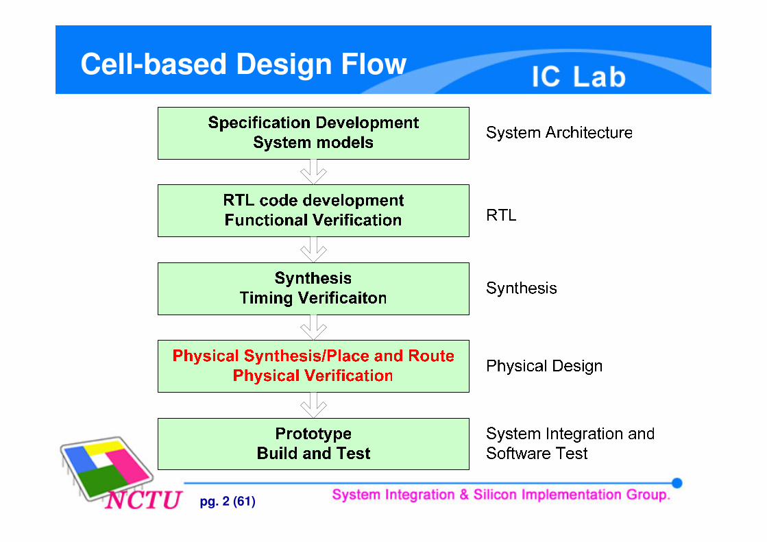
Cell-based Design Flow
pg. 3 (61)
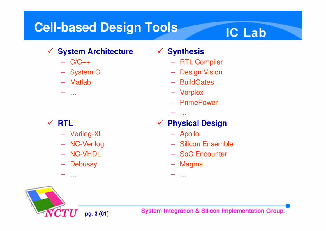
Cell-based Design Tools
� System Architecture– C/C++– System C– Matlab– …
� RTL– Verilog-XL– NC-Verilog– NC-VHDL– Debussy– …
� Synthesis– RTL Compiler– Design Vision– BuildGates– Verplex– PrimePower– …
� Physical Design– Apollo – Silicon Ensemble– SoC Encounter– Magma – …
pg. 4 (61)
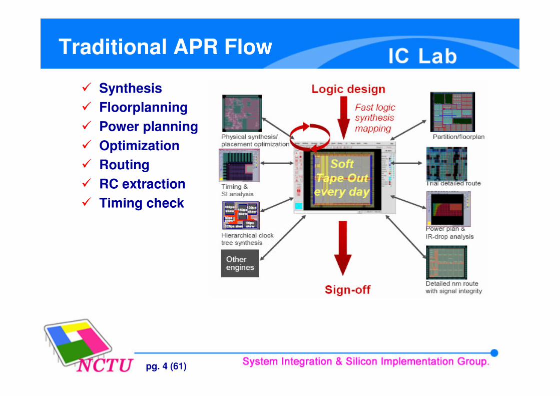
Traditional APR Flow
� Synthesis� Floorplanning� Power planning� Optimization� Routing� RC extraction� Timing check
pg. 5 (61)
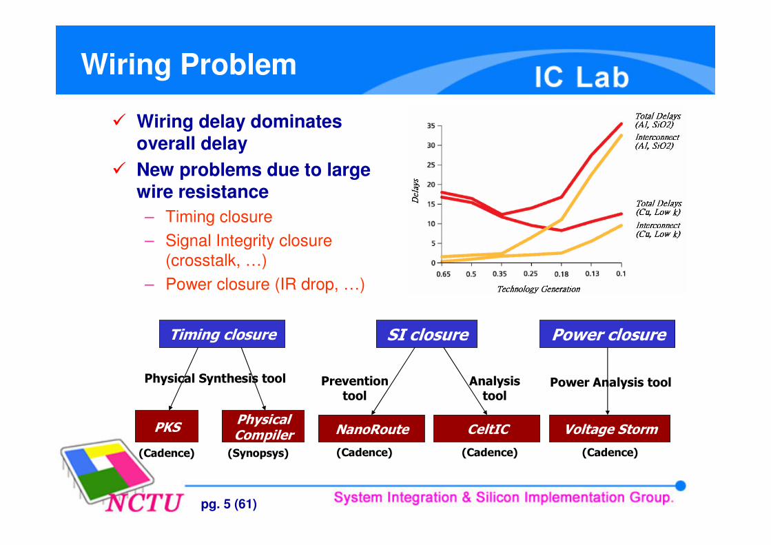
Wiring Problem
� Wiring delay dominates overall delay
� New problems due to largewire resistance– Timing closure– Signal Integrity closure
(crosstalk, …)– Power closure (IR drop, …)
�����������
���� ��������
�������� ��������
��������
� ������ ������
�� �������
���������������
������������
�������� ���������
����� ��������������
�� ����� ������� �� ����� �� ����� �� �����
pg. 6 (61)
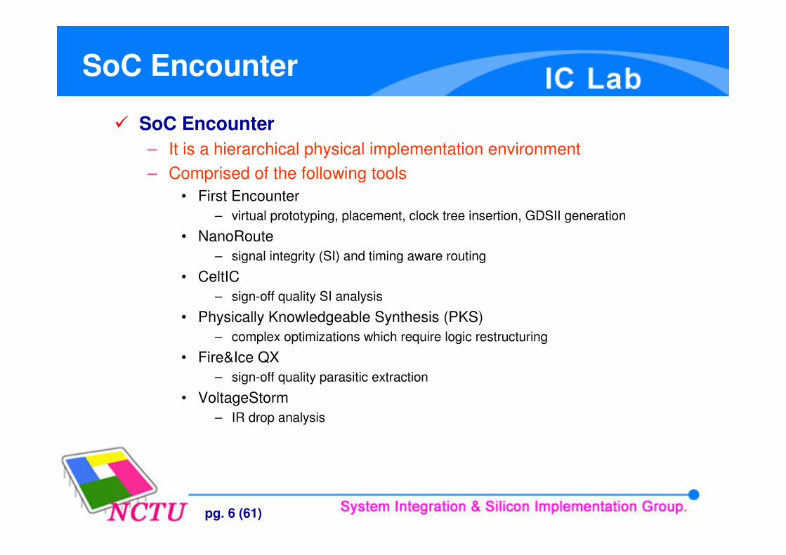
SoC Encounter
� SoC Encounter– It is a hierarchical physical implementation environment– Comprised of the following tools
• First Encounter– virtual prototyping, placement, clock tree insertion, GDSII generation
• NanoRoute– signal integrity (SI) and timing aware routing
• CeltIC– sign-off quality SI analysis
• Physically Knowledgeable Synthesis (PKS)– complex optimizations which require logic restructuring
• Fire&Ice QX– sign-off quality parasitic extraction
• VoltageStorm– IR drop analysis
pg. 7 (61)
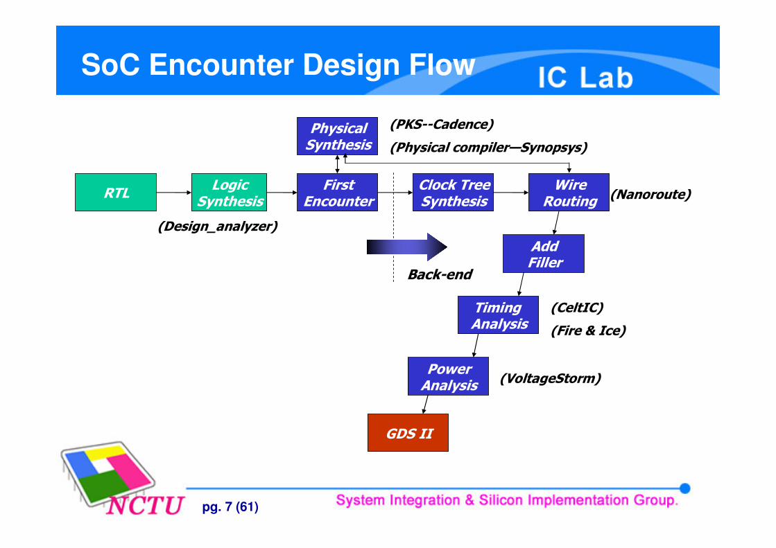
SoC Encounter Design Flow
!�����������
"���#�������
����� ��������
����$������������
���"�����
��������� ���
������� ���
��!
�%����& � ��'��
����((� �����
������ ����������)������
*���������
�� ������
�������
�"����+����
����� �������
,%����
- �$(���
pg. 8 (61)
Getting Started
� Data preparation– Library files
• Technology information and Physical libraries– umc18_5lm.lef– umc18io3v5v_5lm.lef– umc18_5lm_antenna.lef– ram’s.vclef
• Timing libraries– slow.lib– fast.lib– umc18io3v5v_fast.lib– umc18io3v5v_slow.lib– ram’s timing libraries
• CeltIC libraries– umc18.cdB
– Timing constraints• To generate timing constraint files from Design Vision, add the script
write_sdc sdc_filename• Ex: write_sdc CHIP.sdc
pg. 9 (61)
Getting Started (cont.)
� Data preparation (cont.)
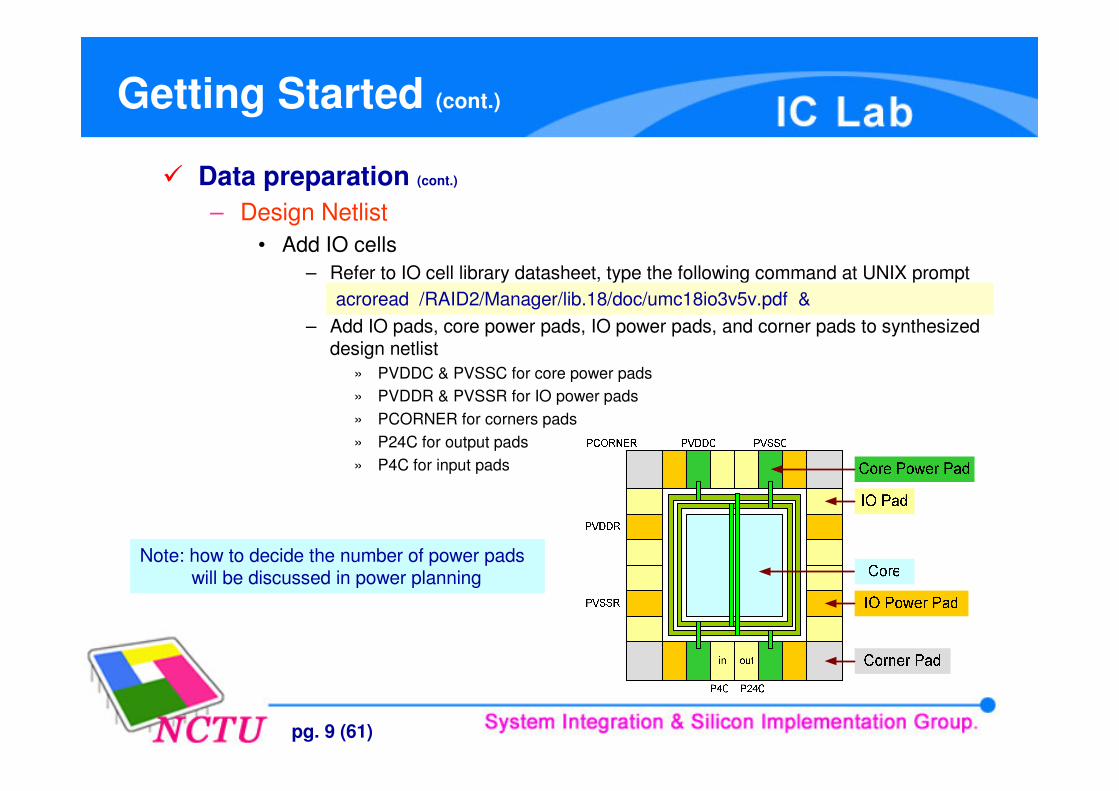
– Design Netlist• Add IO cells
– Refer to IO cell library datasheet, type the following command at UNIX prompt
– Add IO pads, core power pads, IO power pads, and corner pads to synthesized design netlist
» PVDDC & PVSSC for core power pads» PVDDR & PVSSR for IO power pads» PCORNER for corners pads» P24C for output pads» P4C for input pads
acroread /RAID2/Manager/lib.18/doc/umc18io3v5v.pdf &
Note: how to decide the number of power padswill be discussed in power planning
pg. 10 (61)
Getting Started (cont.)
– Design Netlist (cont.)
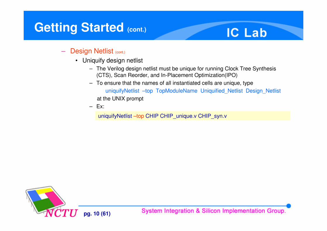
• Uniquify design netlist– The Verilog design netlist must be unique for running Clock Tree Synthesis
(CTS), Scan Reorder, and In-Placement Optimization(IPO)– To ensure that the names of all instantiated cells are unique, type
uniquifyNetlist –top TopModuleName Uniquified_Netlist Design_Netlistat the UNIX prompt
– Ex:
uniquifyNetlist –top CHIP CHIP_unique.v CHIP_syn.v
pg. 11 (61)
Getting Started (cont.)
� Data preparation (cont.)
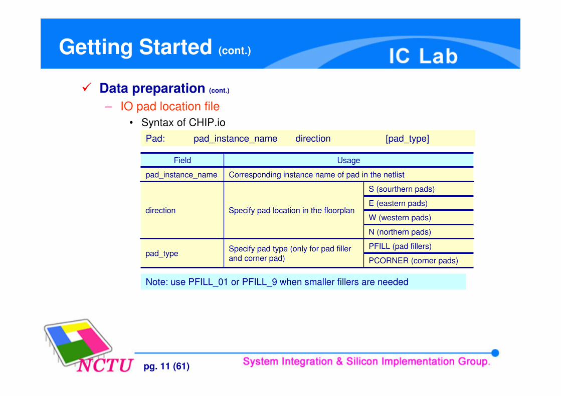
– IO pad location file• Syntax of CHIP.io
Note: use PFILL_01 or PFILL_9 when smaller fillers are needed
PFILL (pad fillers)Specify pad type (only for pad filler and corner pad)
W (western pads)
E (eastern pads)
S (sourthern pads)
PCORNER (corner pads)
N (northern pads)
Specify pad location in the floorplandirection
pad_type
Corresponding instance name of pad in the netlistpad_instance_name
UsageField
Pad: pad_instance_name direction [pad_type]
pg. 12 (61)
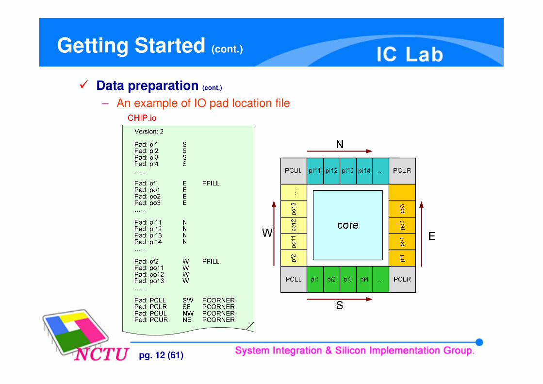
Getting Started (cont.)
� Data preparation (cont.)
– An example of IO pad location file
pg. 13 (61)
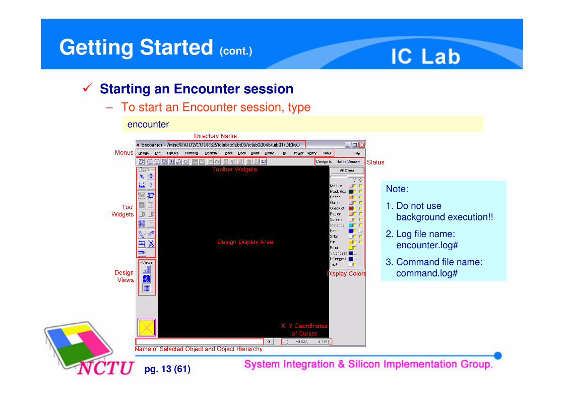
Getting Started (cont.)
� Starting an Encounter session– To start an Encounter session, type
encounter
Note:
1. Do not usebackground execution!!
2. Log file name:encounter.log#
3. Command file name:command.log#
pg. 14 (61)
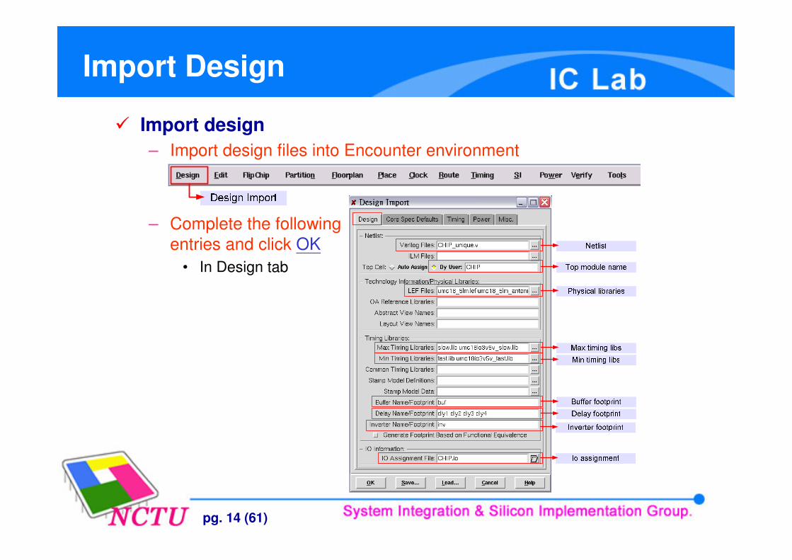
Import Design
� Import design– Import design files into Encounter environment
– Complete the followingentries and click OK
• In Design tab
pg. 15 (61)
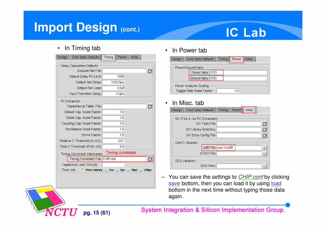
Import Design (cont.)
• In Timing tab
– You can save the settings to CHIP.conf by clicking save bottom, then you can load it by using loadbottom in the next time without typing those data again.
• In Power tab
• In Misc. tab
pg. 16 (61)
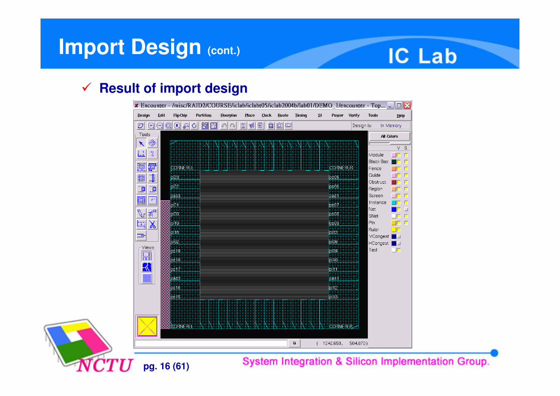
Import Design (cont.)
� Result of import design
pg. 17 (61)
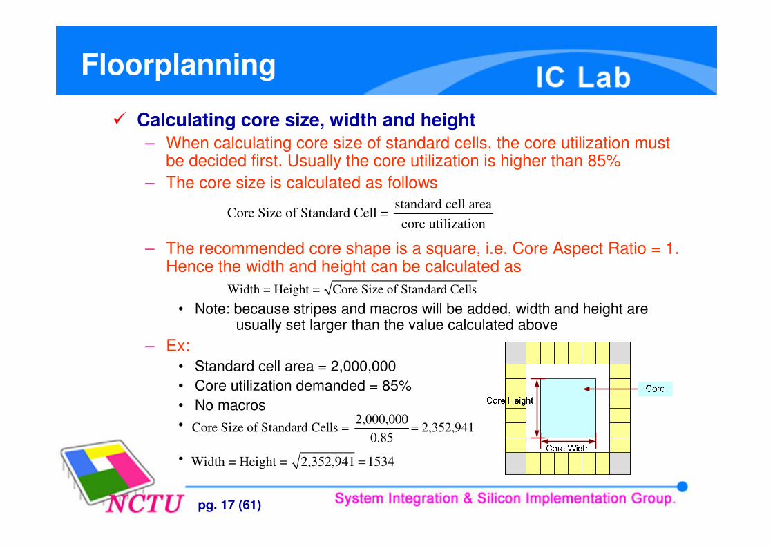
Floorplanning
� Calculating core size, width and height– When calculating core size of standard cells, the core utilization must
be decided first. Usually the core utilization is higher than 85%– The core size is calculated as follows
– The recommended core shape is a square, i.e. Core Aspect Ratio = 1. Hence the width and height can be calculated as
• Note: because stripes and macros will be added, width and height areusually set larger than the value calculated above
– Ex:• Standard cell area = 2,000,000• Core utilization demanded = 85%• No macros•
•
standard cell areaCore Size of Standard Cell =
core utilization
Width = Height = Core Size of Standard Cells
2,000,000Core Size of Standard Cells = = 2,352,941
0.85
Width = Height = 2,352,941 1534=
pg. 18 (61)
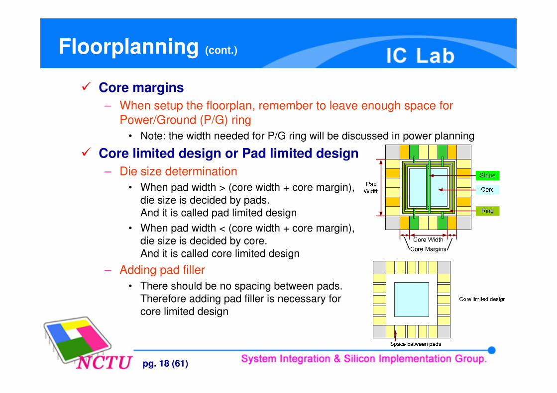
Floorplanning (cont.)
� Core margins– When setup the floorplan, remember to leave enough space for
Power/Ground (P/G) ring• Note: the width needed for P/G ring will be discussed in power planning
� Core limited design or Pad limited design– Die size determination
• When pad width > (core width + core margin),die size is decided by pads.And it is called pad limited design
• When pad width < (core width + core margin),die size is decided by core.And it is called core limited design
– Adding pad filler• There should be no spacing between pads.
Therefore adding pad filler is necessary forcore limited design
pg. 19 (61)
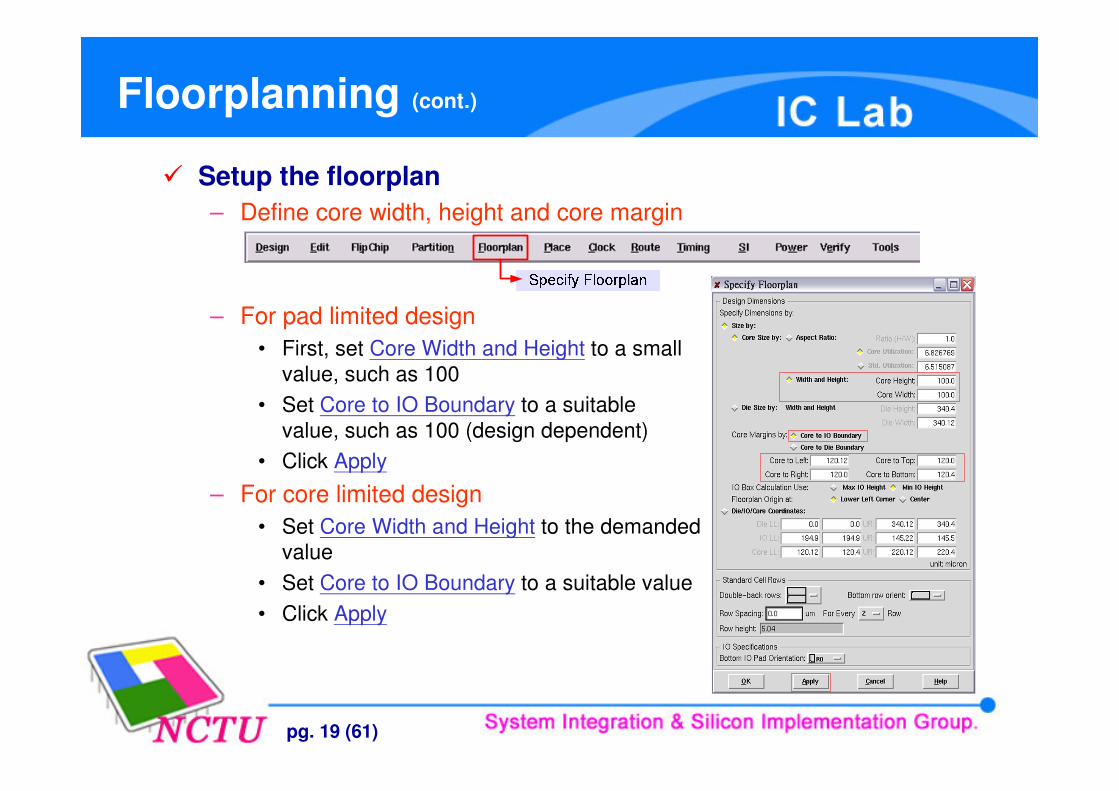
Floorplanning (cont.)
� Setup the floorplan– Define core width, height and core margin
– For pad limited design• First, set Core Width and Height to a small
value, such as 100• Set Core to IO Boundary to a suitable
value, such as 100 (design dependent)• Click Apply
– For core limited design• Set Core Width and Height to the demanded
value• Set Core to IO Boundary to a suitable value• Click Apply
pg. 20 (61)
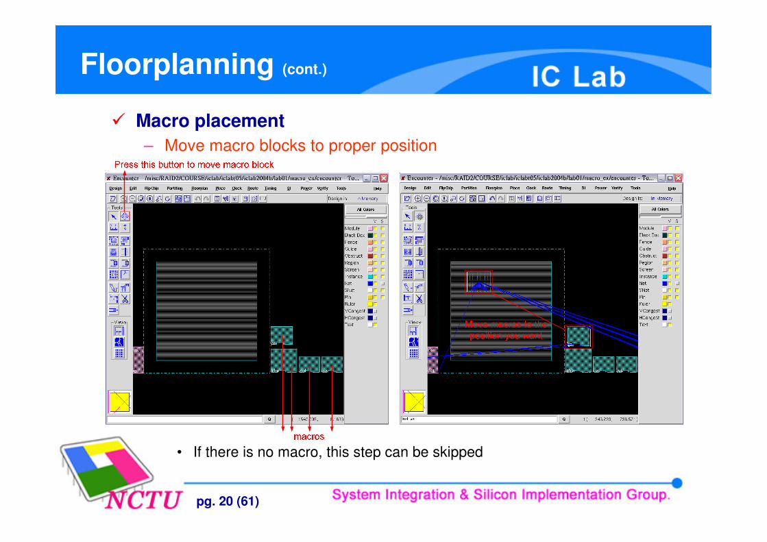
Floorplanning (cont.)
� Macro placement– Move macro blocks to proper position
• If there is no macro, this step can be skipped
pg. 21 (61)
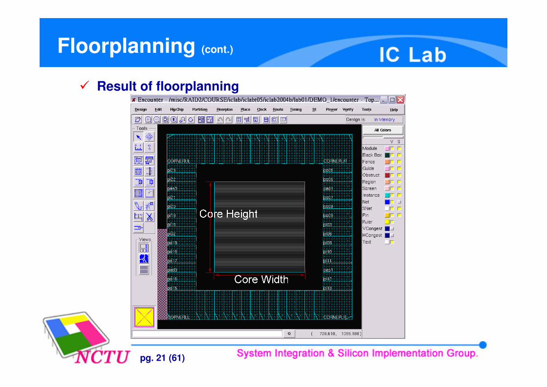
Floorplanning (cont.)
� Result of floorplanning
pg. 22 (61)
Power Planning
� Power issue– Metal migration (also known as electro-migration)
• Under high currents, electron collisions with metal grains cause the metal to move. The metal wire may be open circuit or short circuit.
• Prevention: sizing power supply lines to ensure that the chip does not fail• Experience: make current density of power ring < 1mA/�m
– IR drop• IR drop is the problem of voltage drop of the power and ground due to high
current flowing through the power-ground resistive network• When there are excessive voltage drops in the power network or voltage
rises in the ground network, the device will run at slower speed• IR drop can cause the chip to fail due to
– Performance (circuit running slower than specification)– Functionality problem (setup or hold violations)– Unreliable operation (less noise margin)– Power consumption (leakage power)– Latch up
• Prevention: adding stripes to avoid IR drop on cell’s power line
pg. 23 (61)
Power Planning (cont.)
� Calculating power/ground ring width– Experience
• Gate count = 70 k• 4000 Flip-Flops• 80% FF with dynamic gated clock• Current needed = 0.2mA/MHz
– Note: the value should multiply with 1.8~2 for no gated design
– Example:• Gate count = 200 k• No gated clock• Clock frequency = 20 MHz• Current needed = (200/70) * 0.2 * 20 * 2 = 22.86 mA• Current density < 1mA/�m• The Width of P/G Ring > 22.86 �m• In order to avoid the slot rule of wide metal, the largest width is 20 �m
(process dependent)• Use two set P/G ring for this case
pg. 24 (61)
Power Planning (cont.)
� Calculate stripe set– Experience
• Add one strap set per 100 �m
– Example• Core width = height = 1600• Stripe set added = 15
� Core/IO power pad selection– Core power pad
• One set core power pad (PVDDC along with PVSSC) can provide 40~50mA current
– IO power pad• One set IO power pad (PVDDR along with PVSSR) can provide the power
for– 3~4 output pads, or– 6~8 input pads
pg. 25 (61)
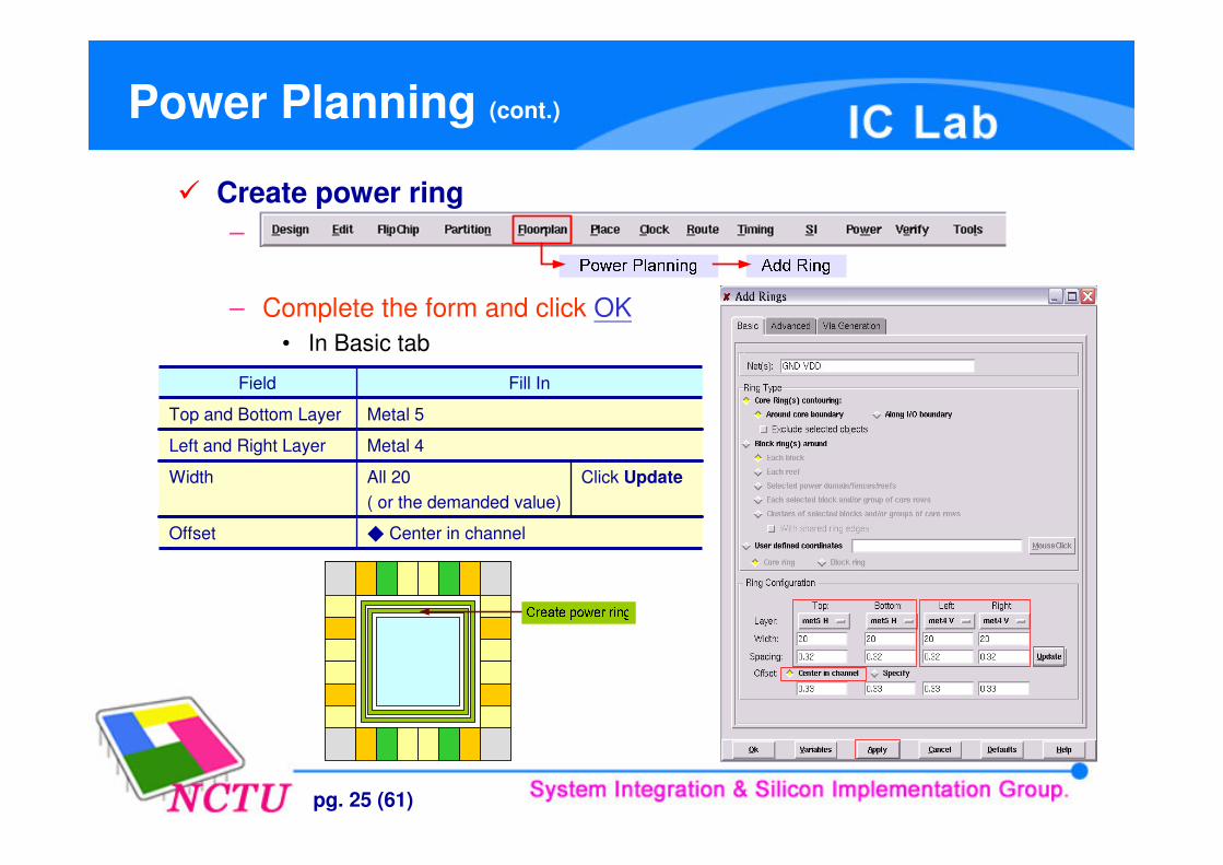
Power Planning (cont.)
� Create power ring–
– Complete the form and click OK• In Basic tab
Click Update
� Center in channelOffset
All 20 ( or the demanded value)
Width
Metal 4Left and Right Layer
Metal 5Top and Bottom Layer
Fill InField
pg. 26 (61)
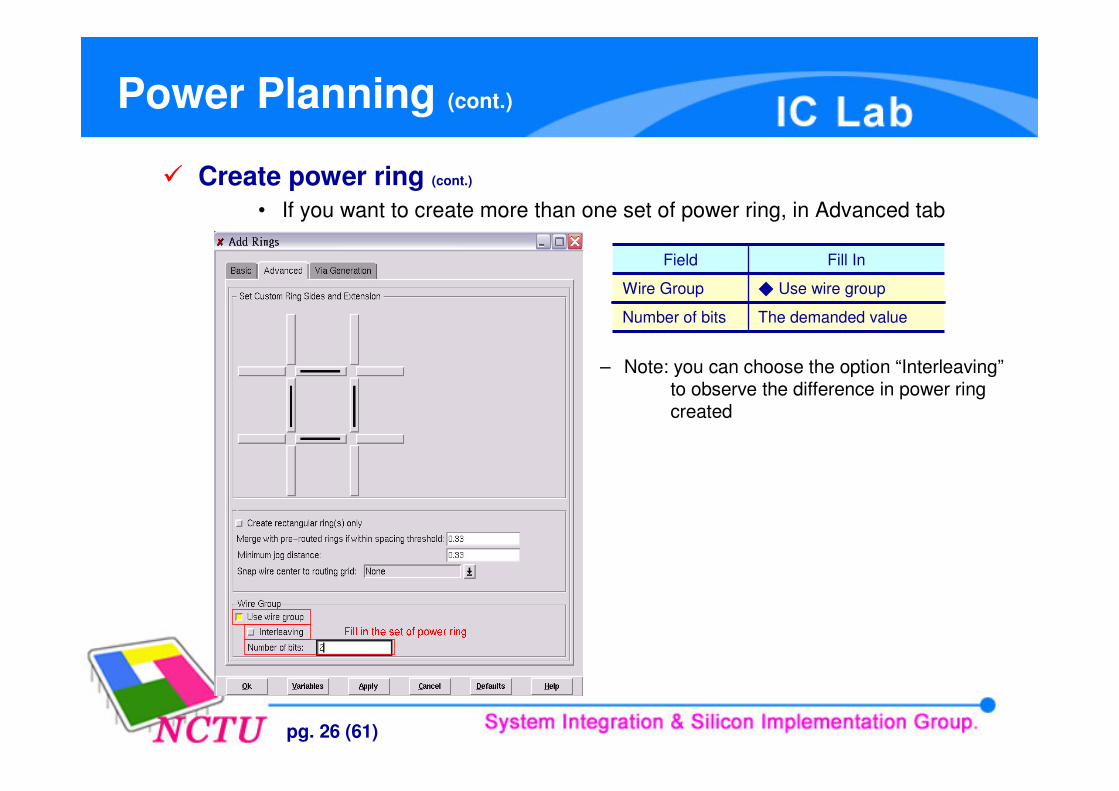
Power Planning (cont.)
� Create power ring (cont.)
• If you want to create more than one set of power ring, in Advanced tab
– Note: you can choose the option “Interleaving”to observe the difference in power ringcreated
The demanded valueNumber of bits
� Use wire groupWire Group
Fill InField
pg. 27 (61)
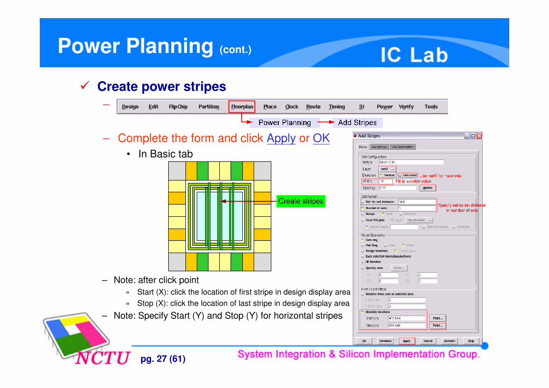
Power Planning (cont.)
� Create power stripes–
– Complete the form and click Apply or OK• In Basic tab
– Note: after click point» Start (X): click the location of first stripe in design display area » Stop (X): click the location of last stripe in design display area
– Note: Specify Start (Y) and Stop (Y) for horizontal stripes
pg. 28 (61)
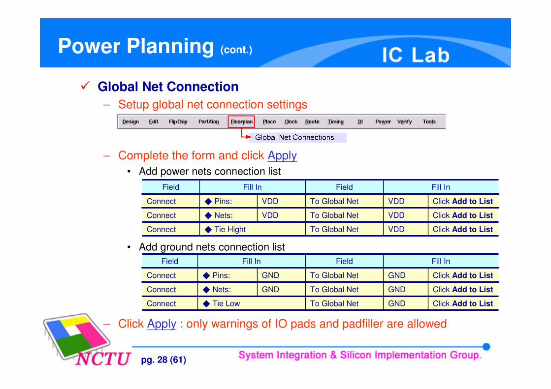
Power Planning (cont.)
� Global Net Connection– Setup global net connection settings
– Complete the form and click Apply• Add power nets connection list
• Add ground nets connection list
– Click Apply : only warnings of IO pads and padfiller are allowed
Click Add to List
Click Add to List
Click Add to List
VDDTo Global NetVDD� Nets:Connect
VDDTo Global Net
Fill InField
VDDTo Global NetVDD� Pins:Connect
� Tie HightConnect
Fill InField
Click Add to List
Click Add to List
Click Add to List
GNDTo Global NetGND� Nets:Connect
GNDTo Global Net
Fill InField
GNDTo Global NetGND� Pins:Connect
� Tie LowConnect
Fill InField
pg. 29 (61)
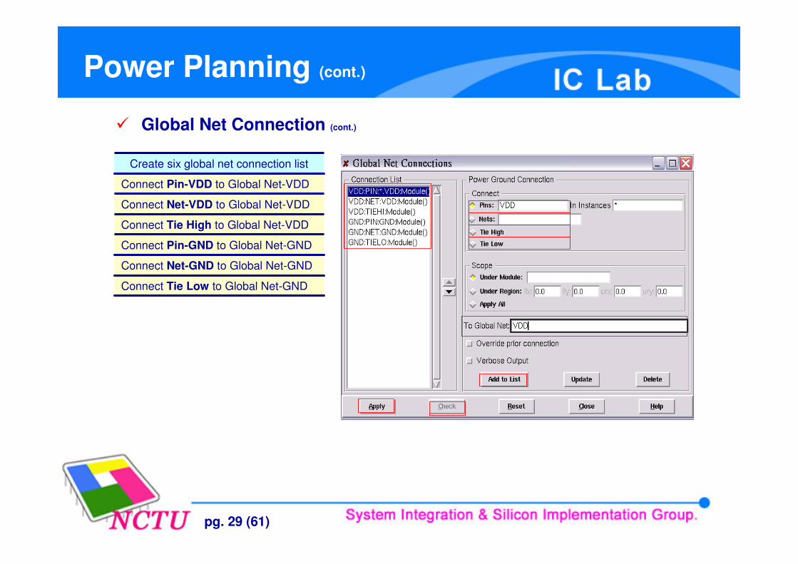
Power Planning (cont.)
� Global Net Connection (cont.)
Connect Tie Low to Global Net-GND
Connect Net-GND to Global Net-GND
Connect Tie High to Global Net-VDD
Connect Net-VDD to Global Net-VDD
Connect Pin-VDD to Global Net-VDD
Connect Pin-GND to Global Net-GND
Create six global net connection list
pg. 30 (61)
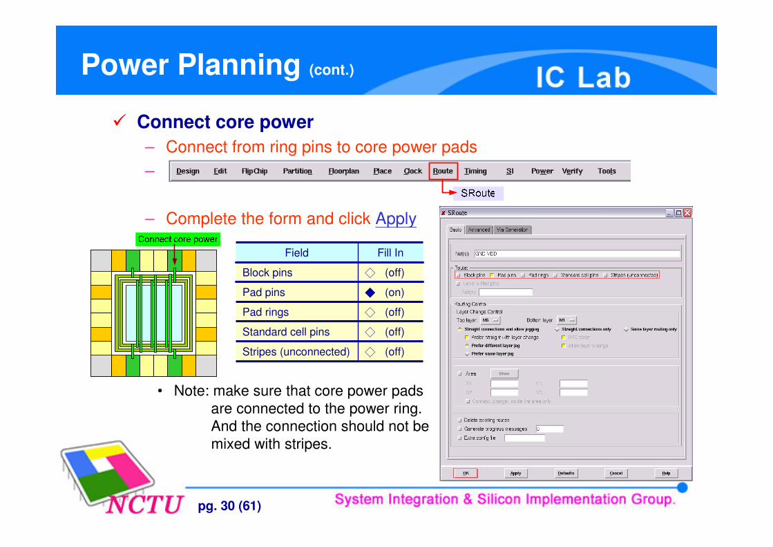
Power Planning (cont.)
� Connect core power– Connect from ring pins to core power pads–
– Complete the form and click Apply
� (off)Pad rings
� (off)Standard cell pins
� (on)Pad pins
� (off)Block pins
� (off)Stripes (unconnected)
Fill InField
• Note: make sure that core power padsare connected to the power ring.And the connection should not bemixed with stripes.
pg. 31 (61)
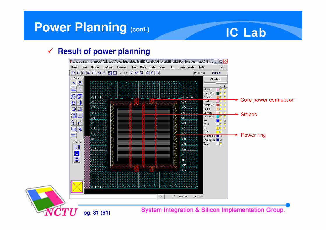
Power Planning (cont.)
� Result of power planning
pg. 32 (61)
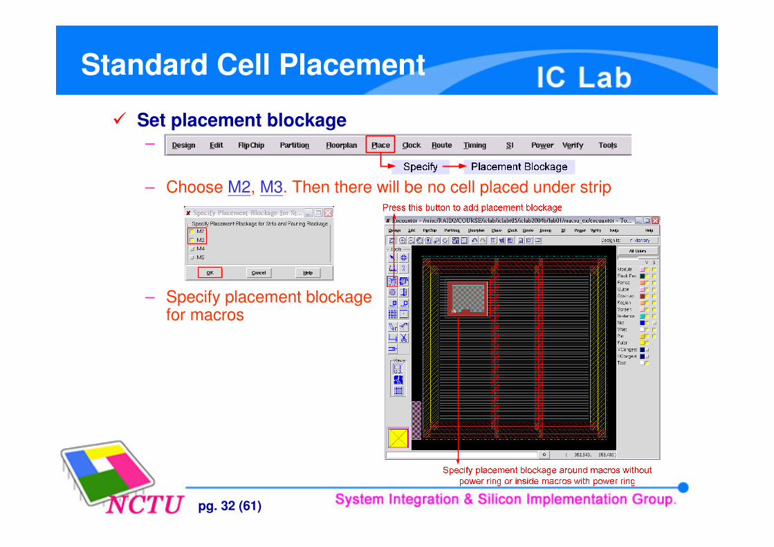
Standard Cell Placement
� Set placement blockage–
– Choose M2, M3. Then there will be no cell placed under strip
– Specify placement blockagefor macros
pg. 33 (61)
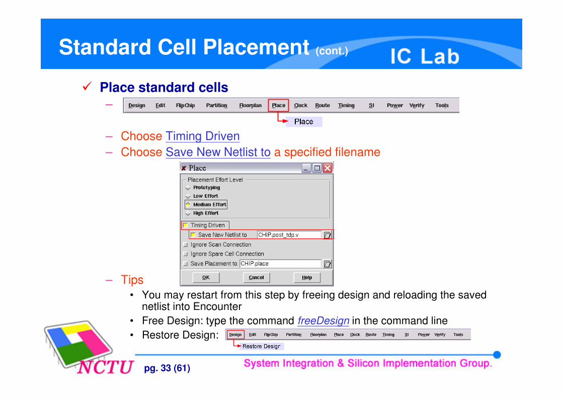
Standard Cell Placement (cont.)
� Place standard cells–
– Choose Timing Driven– Choose Save New Netlist to a specified filename
– Tips• You may restart from this step by freeing design and reloading the saved
netlist into Encounter• Free Design: type the command freeDesign in the command line• Restore Design:
pg. 34 (61)
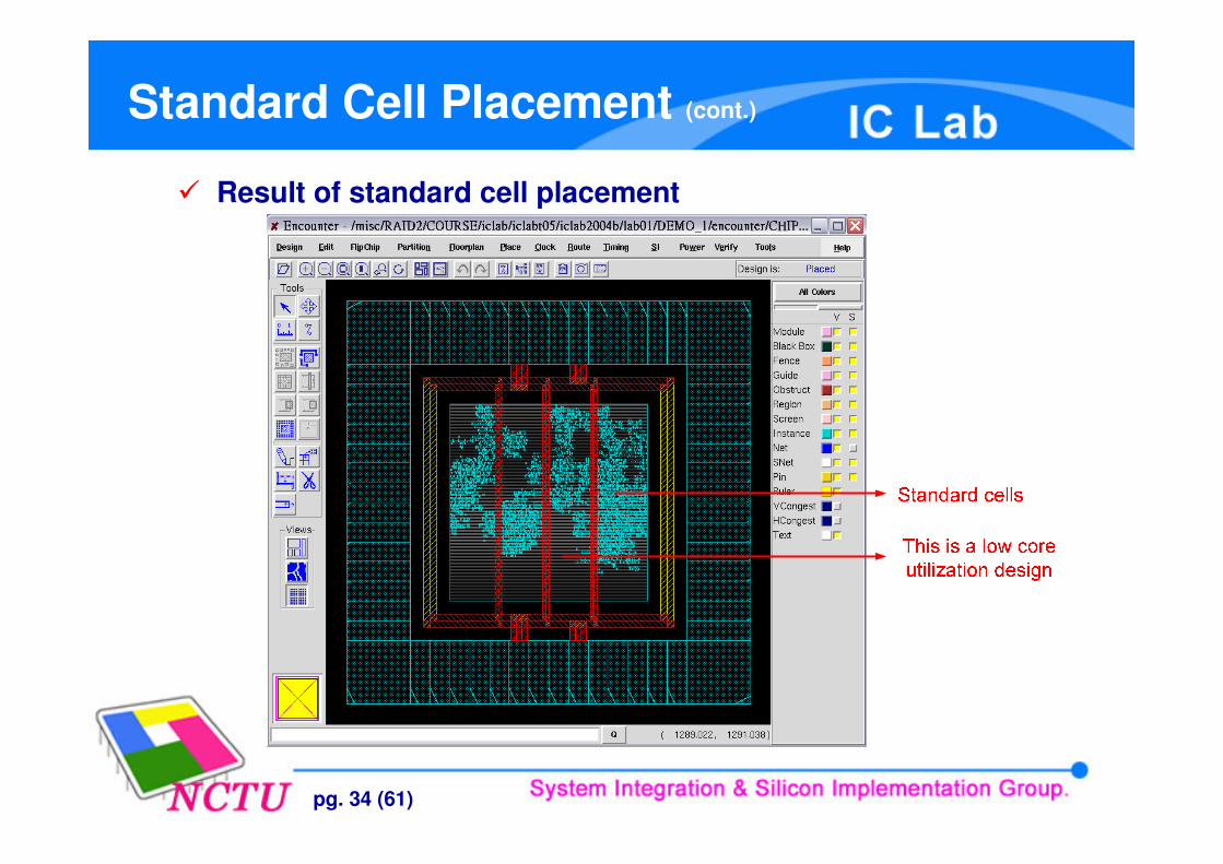
Standard Cell Placement (cont.)
� Result of standard cell placement
pg. 35 (61)
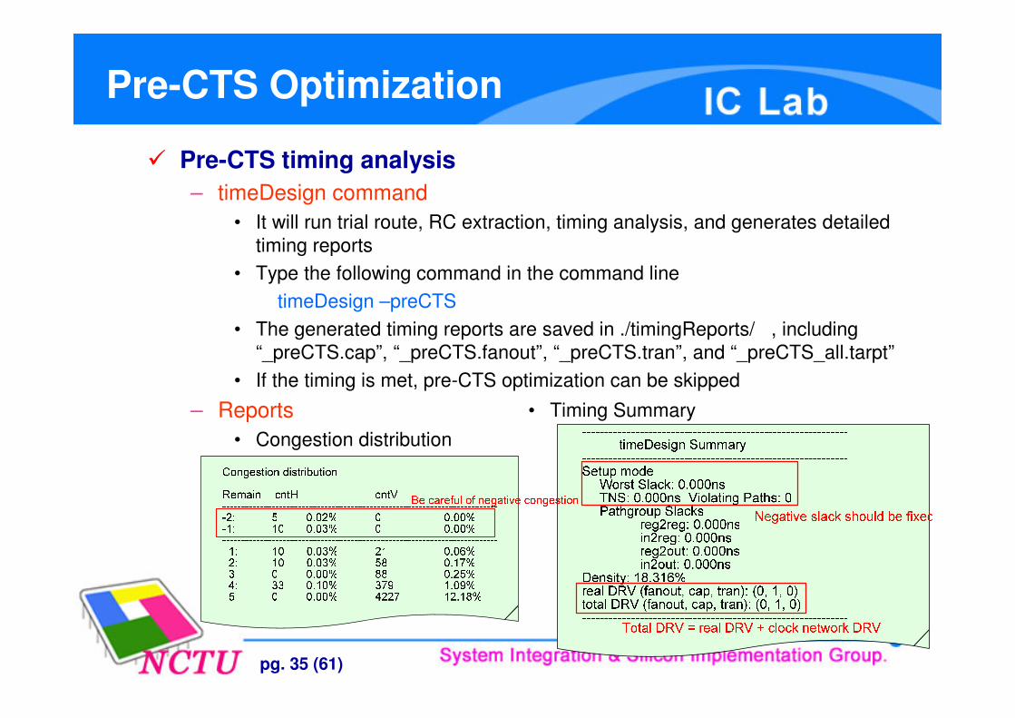
Pre-CTS Optimization
� Pre-CTS timing analysis– timeDesign command
• It will run trial route, RC extraction, timing analysis, and generates detailed timing reports
• Type the following command in the command linetimeDesign –preCTS
• The generated timing reports are saved in ./timingReports/ , including “_preCTS.cap”, “_preCTS.fanout”, “_preCTS.tran”, and “_preCTS_all.tarpt”
• If the timing is met, pre-CTS optimization can be skipped
– Reports• Congestion distribution
• Timing Summary
pg. 36 (61)
Pre-CTS Optimization (cont.)
� Pre-CTS optimization– optDesign command
• It will repair– Setup slack, Setup times– Design rule violations (DRVs), Remaining DRVs
• To optimize timing placed design for the first time with ideal clocksoptDesign –preCTS
• To further optimize a design after above command executionoptDesign –preCTS –incr
pg. 37 (61)
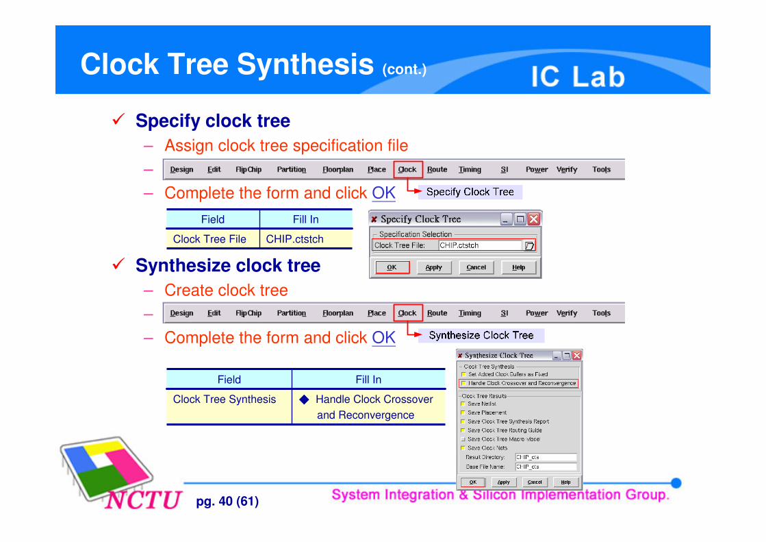
Clock Tree Synthesis
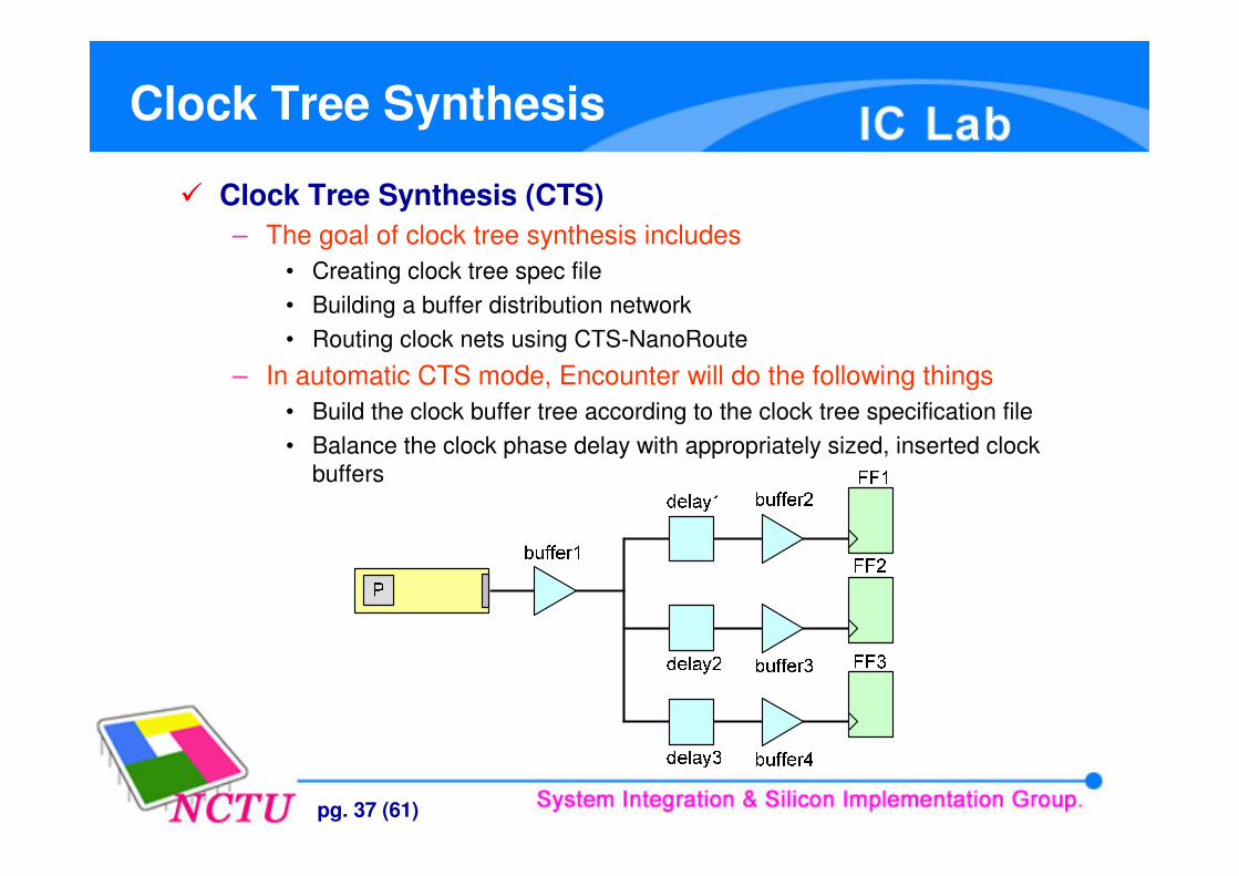
� Clock Tree Synthesis (CTS)– The goal of clock tree synthesis includes
• Creating clock tree spec file• Building a buffer distribution network• Routing clock nets using CTS-NanoRoute
– In automatic CTS mode, Encounter will do the following things• Build the clock buffer tree according to the clock tree specification file• Balance the clock phase delay with appropriately sized, inserted clock
buffers
pg. 38 (61)
Clock Tree Synthesis (cont.)
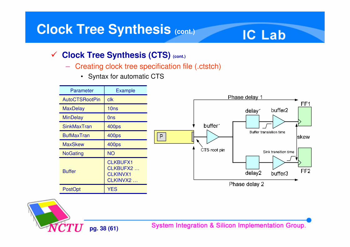
� Clock Tree Synthesis (CTS) (cont.)
– Creating clock tree specification file (.ctstch)• Syntax for automatic CTS
400psBufMaxTran
400psSinkMaxTran
NONoGating
CLKBUFX1 CLKBUFX2 …CLKINVX1 CLKINVX2 …
Buffer
400psMaxSkew
0nsMinDelay
10nsMaxDelay
clkAutoCTSRootPin
YESPostOpt
ExampleParameter
pg. 39 (61)
Clock Tree Synthesis (cont.)
� Clock Tree Synthesis (CTS) (cont.)
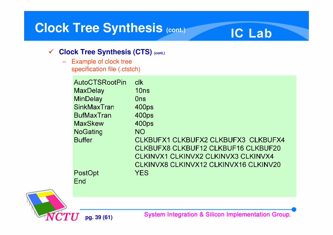
– Example of clock tree specification file (.ctstch)
pg. 40 (61)
Clock Tree Synthesis (cont.)
� Specify clock tree– Assign clock tree specification file–– Complete the form and click OK
� Synthesize clock tree– Create clock tree–– Complete the form and click OK
CHIP.ctstchClock Tree File
Fill InField
� Handle Clock Crossoverand Reconvergence
Clock Tree Synthesis
Fill InField

pg. 41 (61)
Post-CTS Optimization
� Post-CTS timing analysis– timeDesign command
• Type the following command in the command line to check setup timetimeDesign –postCTS
• Type the following command in the command line to check hold timetimeDesign –postCTS –hold
• The generated timing reports are saved in ./timingReports/ , including “_postCTS.cap”, “_postCTS.fanout”, “_postCTS.tran”, and “_postCTS_all.tarpt”
� Post-CTS optimization– optDesign command
• To correct setup violations and design rule violationsoptDesign –postCTS
• To correct hold violationsoptDesign –postCTS –hold
pg. 42 (61)
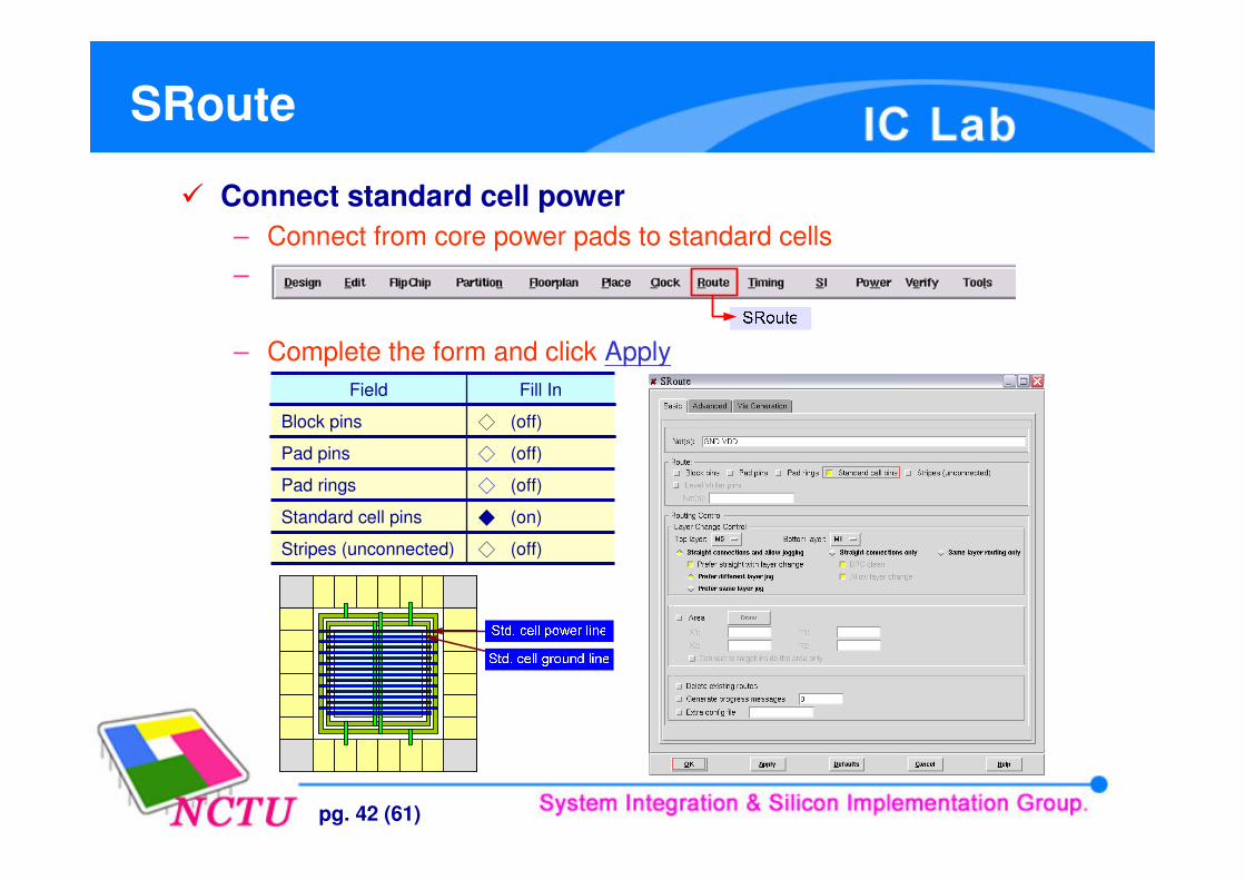
SRoute
� Connect standard cell power– Connect from core power pads to standard cells–
– Complete the form and click Apply
� (off)Pad rings
� (on)Standard cell pins
� (off)Pad pins
� (off)Block pins
� (off)Stripes (unconnected)
Fill InField
pg. 43 (61)
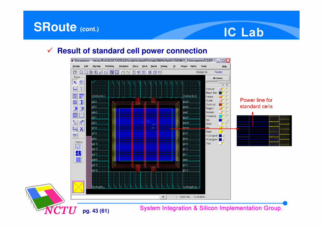
SRoute (cont.)
� Result of standard cell power connection

pg. 44 (61)
NanoRoute
� Process Antenna Effect (PAE)– PAE phenomenon
• During deep submicron wafer fabrication, gate damage can occur when excessive static charges accumulate and discharge, passing current through a gate
– The cause of PAE• If the area of the layer connected directly to the gate is large (or the layer
connected to the gate through lower layers is large) relative to the area of the gate, the discharge of enough static charges can damage the oxide that insulates the gate and cause the chip to fail
– Prevention of PAE• Method 1: changing the routing so the routing layers connected to a gate or
connected to a gate through lower layers are not so large• Method 2: inserting diodes that protect the gate by providing an alternate
path to discharge the static charge
pg. 45 (61)
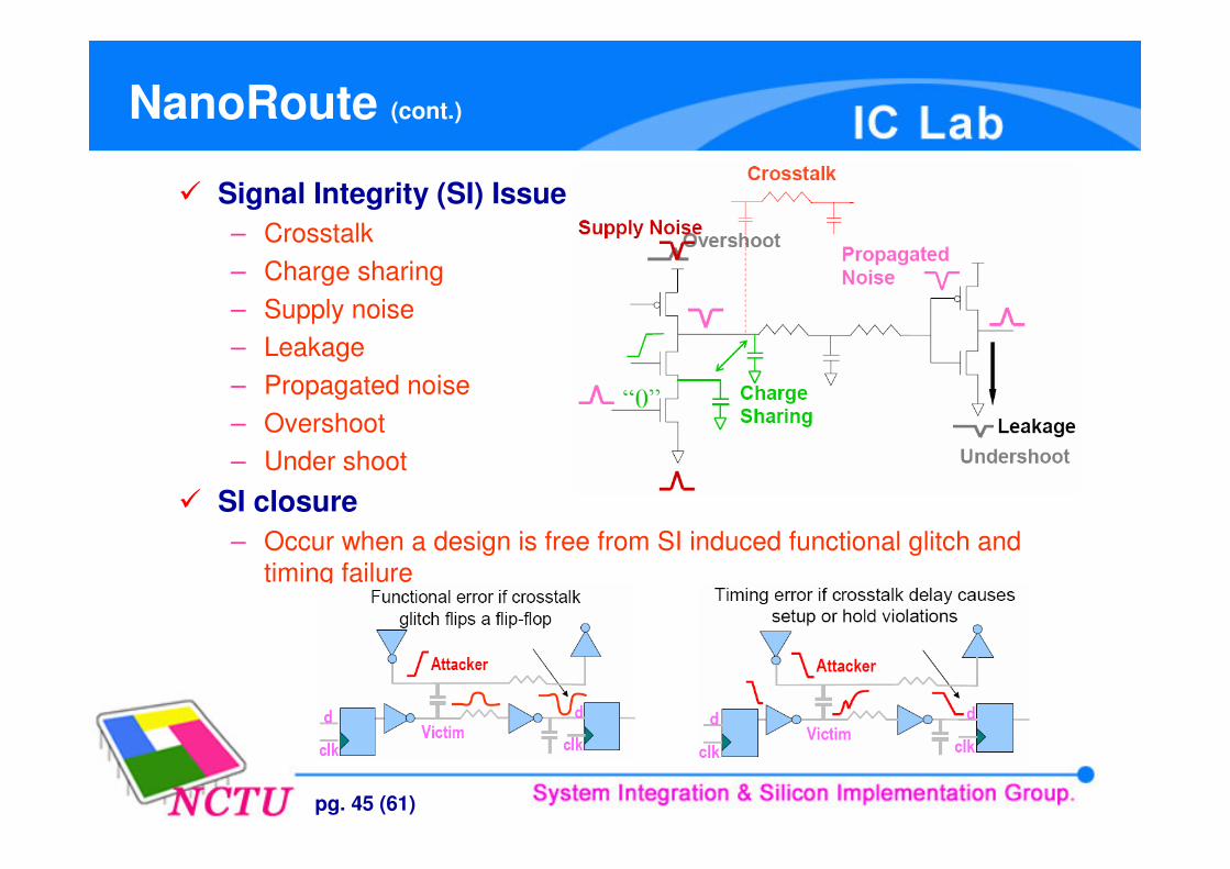
NanoRoute (cont.)
� Signal Integrity (SI) Issue– Crosstalk– Charge sharing– Supply noise– Leakage– Propagated noise– Overshoot– Under shoot
� SI closure– Occur when a design is free from SI induced functional glitch and
timing failure
pg. 46 (61)
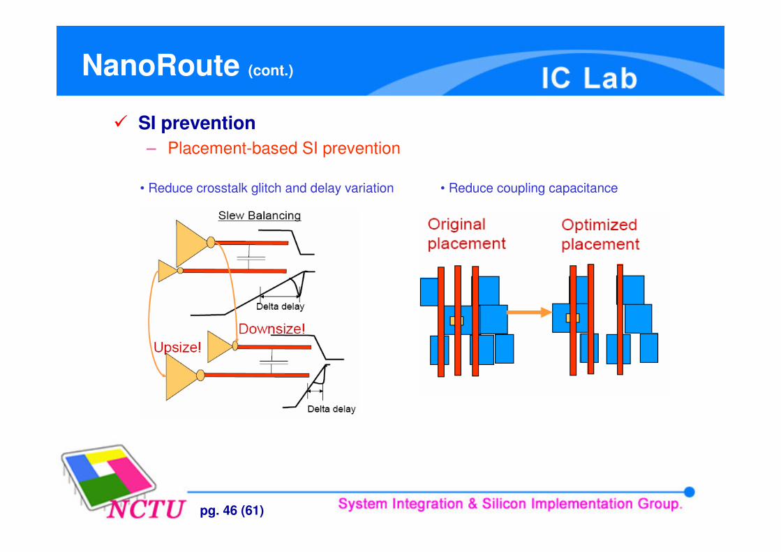
NanoRoute (cont.)
� SI prevention– Placement-based SI prevention
• Reduce crosstalk glitch and delay variation • Reduce coupling capacitance
pg. 47 (61)
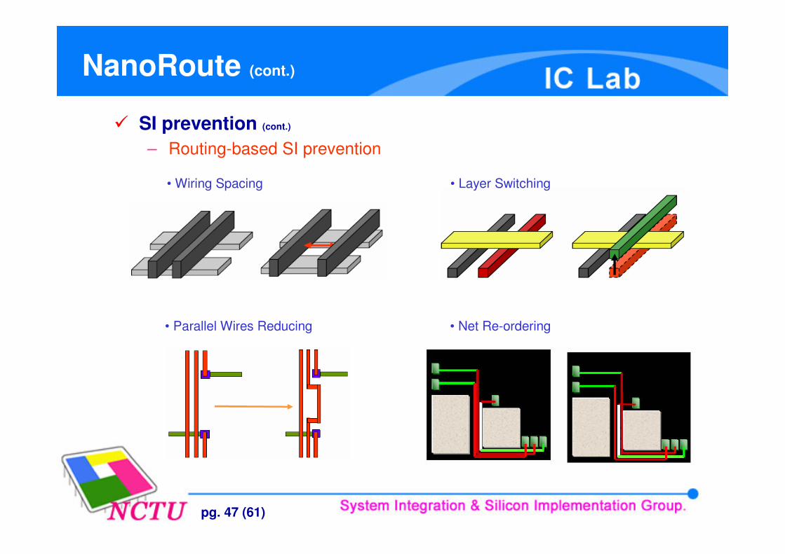
NanoRoute (cont.)
� SI prevention (cont.)
– Routing-based SI prevention
• Wiring Spacing • Layer Switching
• Parallel Wires Reducing • Net Re-ordering
pg. 48 (61)
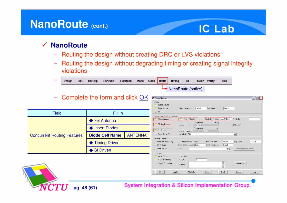
NanoRoute (cont.)
� NanoRoute– Routing the design without creating DRC or LVS violations– Routing the design without degrading timing or creating signal integrity
violations–
– Complete the form and click OK
ANTENNADiode Cell Name
� SI Driven
� Insert Diodes
� Fix Antenna
� Timing Driven
Concurrent Routing Features
Fill InField
pg. 49 (61)
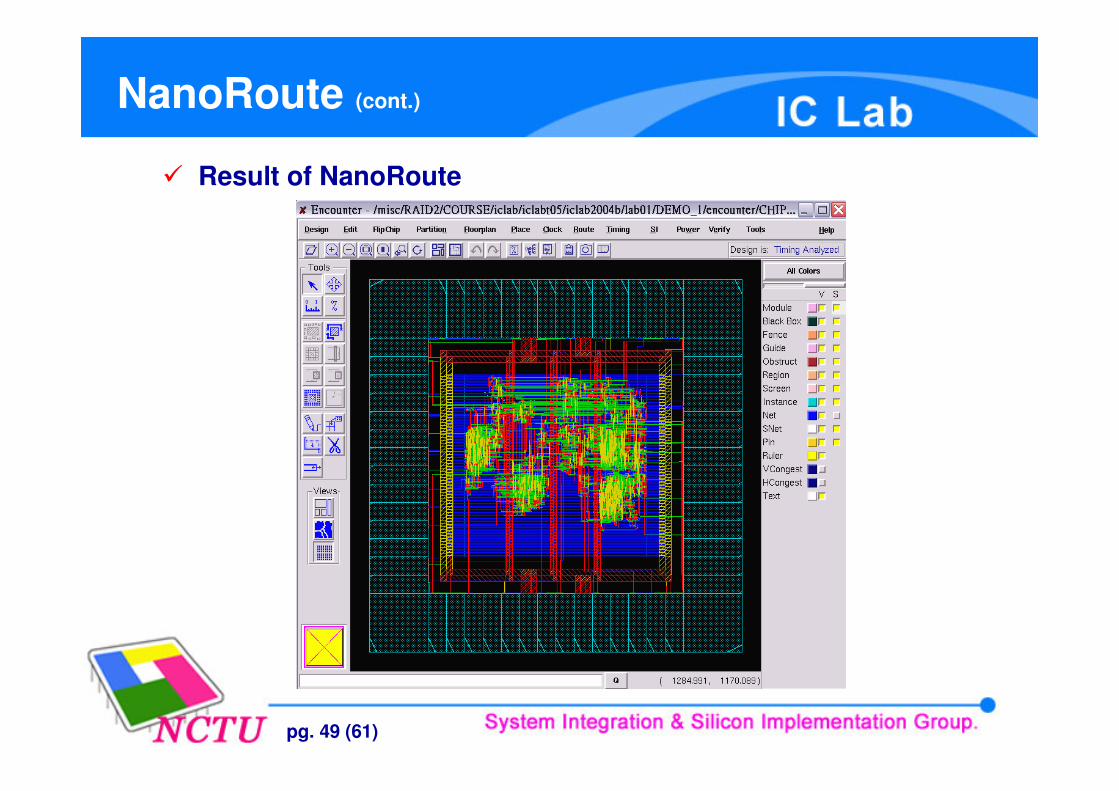
NanoRoute (cont.)
� Result of NanoRoute
pg. 50 (61)
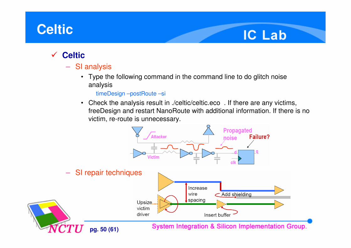
Celtic
� Celtic– SI analysis
• Type the following command in the command line to do glitch noise analysis
timeDesign –postRoute –si
• Check the analysis result in ./celtic/celtic.eco . If there are any victims, freeDesign and restart NanoRoute with additional information. If there is no victim, re-route is unnecessary.
– SI repair techniques
pg. 51 (61)
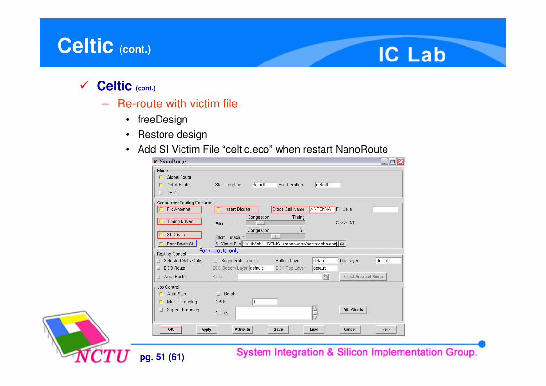
Celtic (cont.)
� Celtic (cont.)
– Re-route with victim file• freeDesign• Restore design• Add SI Victim File “celtic.eco” when restart NanoRoute
pg. 52 (61)
Post-Route Optimization
� Post-Route timing analysis– timeDesign command
• Type the following command in the command line to check setup timetimeDesign –postRoute
• Type the following command in the command line to check hold timetimeDesign –postRoute –hold
• The generated timing reports are saved in ./timingReports/ , including “_postRoute.cap”, “_postRoute.fanout”, “_postRoute.tran”, and “_postRoute_all.tarpt”
� Post-Route optimization– optDesign command
• To correct setup violations and design rule violationsoptDesign –postRoute
• To correct hold violationsoptDesign –postRoute –hold
pg. 53 (61)
Add Filler
� Adding filler cells– Purpose of adding filler cells
• Fill all the gaps between standard cell instances• Provide decoupling capacitances to complete connections in the standard
cell rows
– Metal filler inserted after routing, but before parasitic extraction and GDSII out
– Command• Execute the following command in the encounter prompt
source run_addfiller.cmd
pg. 54 (61)
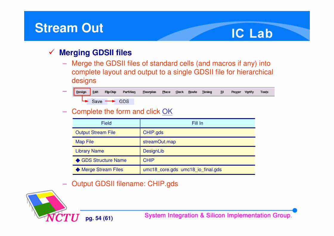
Stream Out
� Merging GDSII files– Merge the GDSII files of standard cells (and macros if any) into
complete layout and output to a single GDSII file for hierarchical designs
–
– Complete the form and click OK
– Output GDSII filename: CHIP.gds
streamOut.mapMap File
CHIP� GDS Structure Name
umc18_core.gds umc18_io_final.gds� Merge Stream Files
DesignLibLibrary Name
CHIP.gdsOutput Stream File
Fill InField
pg. 55 (61)
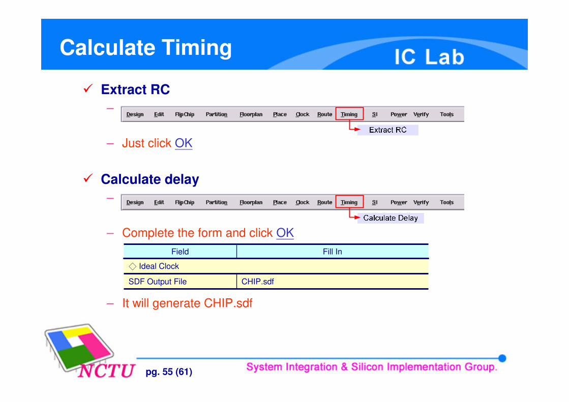
Calculate Timing
� Extract RC–
– Just click OK
� Calculate delay–
– Complete the form and click OK
– It will generate CHIP.sdf
� Ideal Clock
CHIP.sdfSDF Output File
Fill InField
pg. 56 (61)
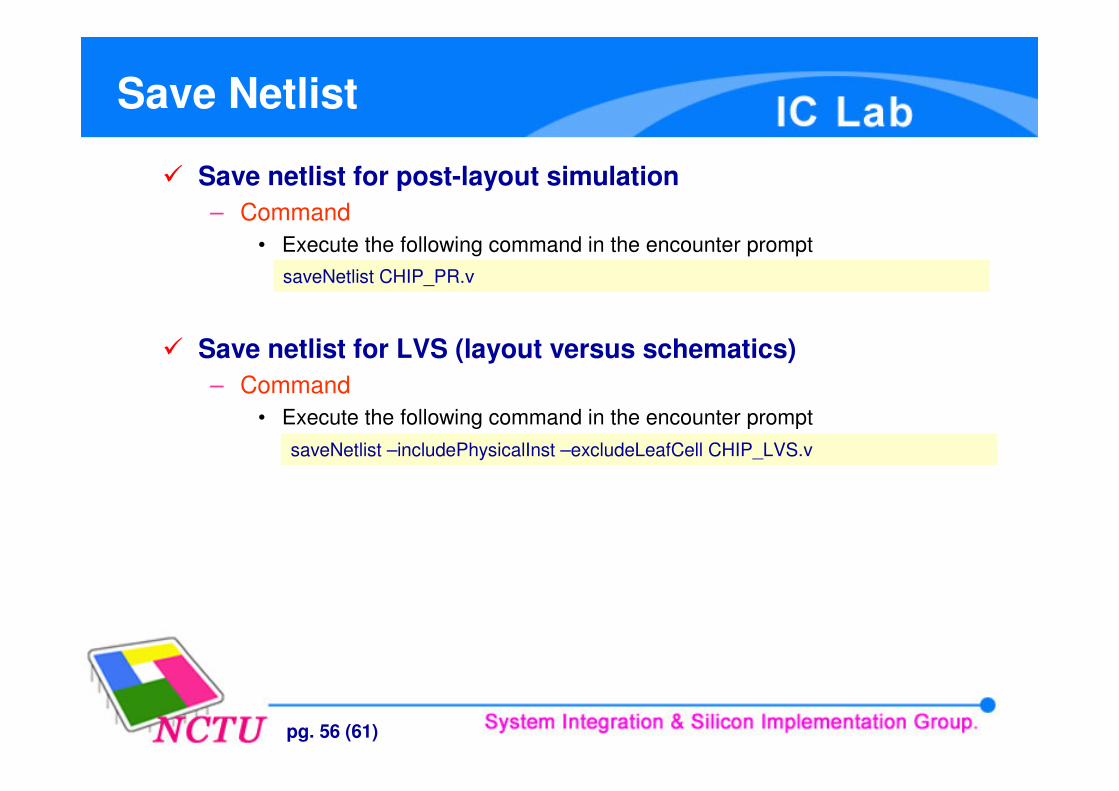
Save Netlist
� Save netlist for post-layout simulation– Command
• Execute the following command in the encounter prompt
� Save netlist for LVS (layout versus schematics)– Command
• Execute the following command in the encounter prompt
saveNetlist CHIP_PR.v
saveNetlist –includePhysicalInst –excludeLeafCell CHIP_LVS.v
pg. 57 (61)
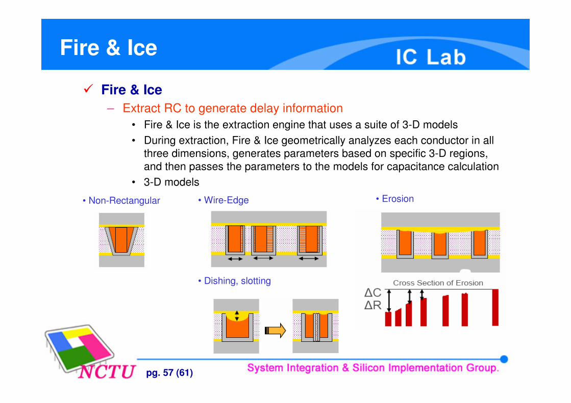
Fire & Ice
� Fire & Ice– Extract RC to generate delay information
• Fire & Ice is the extraction engine that uses a suite of 3-D models• During extraction, Fire & Ice geometrically analyzes each conductor in all
three dimensions, generates parameters based on specific 3-D regions, and then passes the parameters to the models for capacitance calculation
• 3-D models
• Non-Rectangular • Wire-Edge
• Dishing, slotting
• Erosion
pg. 58 (61)
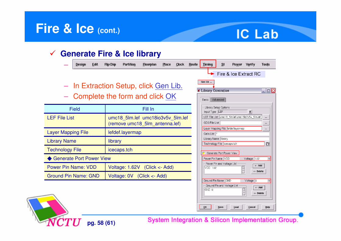
Fire & Ice (cont.)
� Generate Fire & Ice library–
– In Extraction Setup, click Gen Lib.– Complete the form and click OK
Voltage: 1.62V (Click <- Add)Power Pin Name: VDD
� Generate Port Power View
lefdef.layermapLayer Mapping File
icecaps.tchTechnology File
Voltage: 0V (Click <- Add)Ground Pin Name: GND
libraryLibrary Name
umc18_5lm.lef umc18io3v5v_5lm.lef (remove umc18_5lm_antenna.lef)
LEF File List
Fill InField
pg. 59 (61)
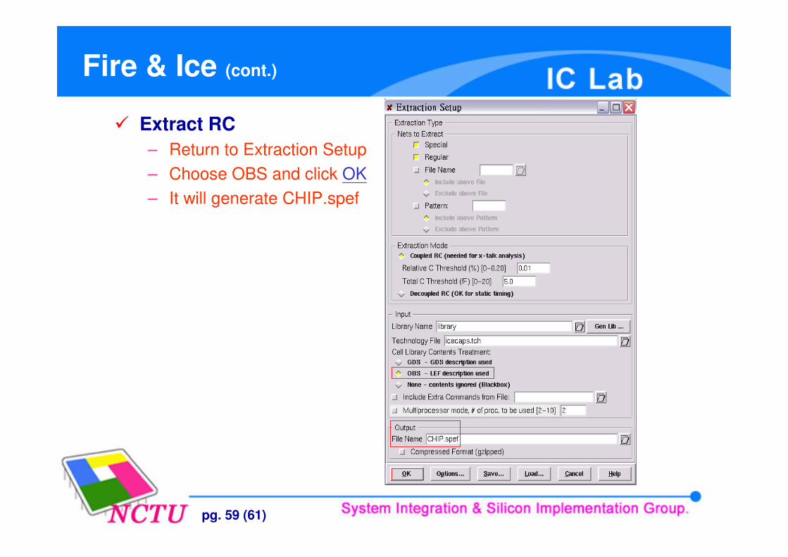
Fire & Ice (cont.)
� Extract RC– Return to Extraction Setup– Choose OBS and click OK– It will generate CHIP.spef
pg. 60 (61)
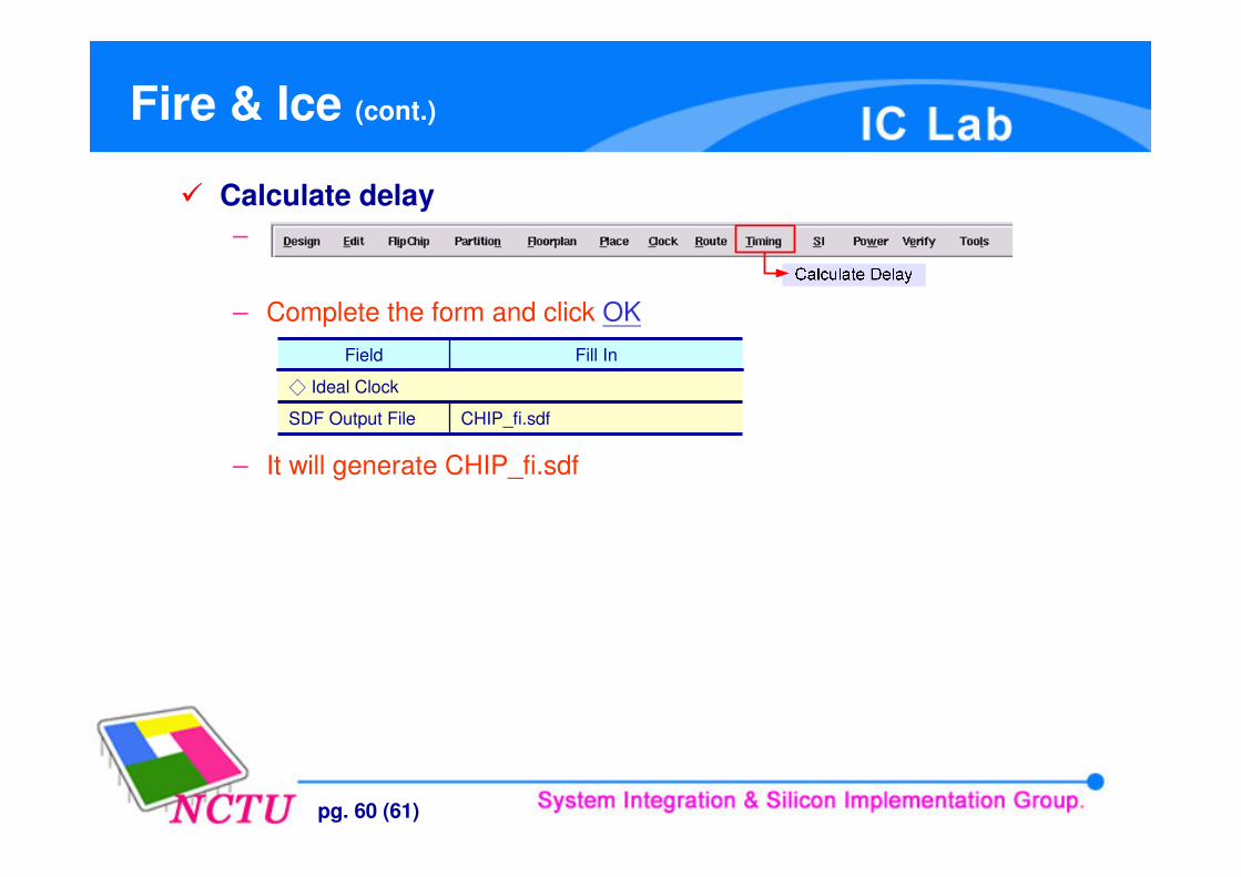
Fire & Ice (cont.)
� Calculate delay–
– Complete the form and click OK
– It will generate CHIP_fi.sdf
� Ideal Clock
CHIP_fi.sdfSDF Output File
Fill InField
pg. 61 (61)
Summary of Output Files
� The following files will be generated after entire APR complete– CHIP.gds
• Layout file for Calibre DRC (Design Rule Check)
– CHIP_PR.v• Netlist for post-layout simulation
– CHIP_LVS.v• Netlist for Calibre LVS (Layout Versus Schematics)
– CHIP.sdf• Timing delay file generated by SoC Encounter (default)
– CHIP_fi.sdf• Timing delay file generated by Soc Encounter (Fire&Ice)