NMT Senior Design
45
EM FIELD MEASUREMENT MODULE FOR EMBEDDED COMPUTING By: Lara Cowan Antonio Jaramillo Shawn Knapp David Yazzie NMT EE Senior Design Team C Submitted in Partial Fulfillment of the Requirements for the Bachelor of Science in Electrical Engineering New Mexico Institute of Mining and Technology Department of Electrical Engineering Socorro, NM May 4 th , 2005
-
Upload
antonio-jaramillo -
Category
Documents
-
view
43 -
download
0
Transcript of NMT Senior Design
EM FIELD MEASUREMENT MODULE FOR EMBEDDED COMPUTING
By:Lara Cowan
Antonio JaramilloShawn KnappDavid Yazzie
NMT EE Senior Design Team C
Submitted in Partial Fulfillmentof the Requirements for the
Bachelor of Science in Electrical Engineering
New Mexico Institute of Mining and TechnologyDepartment of Electrical Engineering
Socorro, NM
May 4th, 2005
Abstract
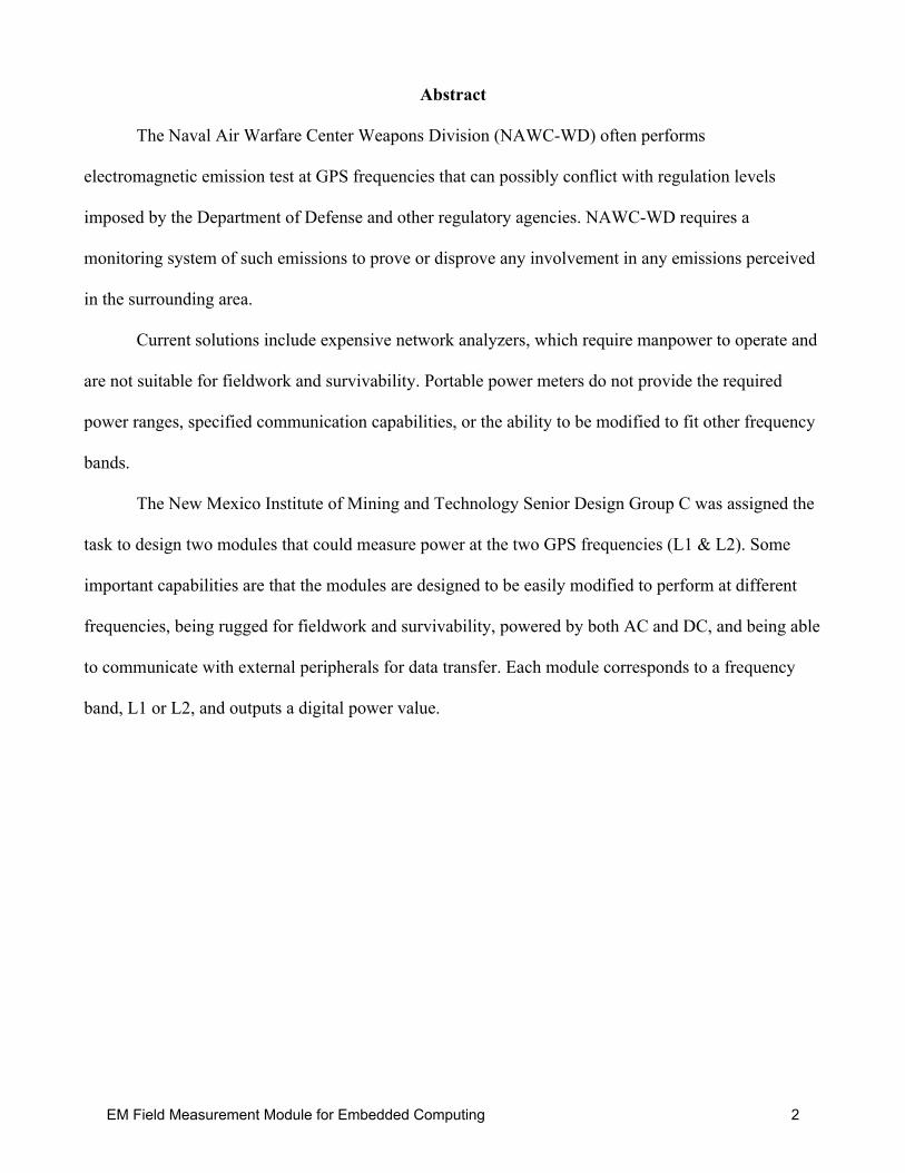
The Naval Air Warfare Center Weapons Division (NAWC-WD) often performs
electromagnetic emission test at GPS frequencies that can possibly conflict with regulation levels
imposed by the Department of Defense and other regulatory agencies. NAWC-WD requires a
monitoring system of such emissions to prove or disprove any involvement in any emissions perceived
in the surrounding area.
Current solutions include expensive network analyzers, which require manpower to operate and
are not suitable for fieldwork and survivability. Portable power meters do not provide the required
power ranges, specified communication capabilities, or the ability to be modified to fit other frequency
bands.
The New Mexico Institute of Mining and Technology Senior Design Group C was assigned the
task to design two modules that could measure power at the two GPS frequencies (L1 & L2). Some
important capabilities are that the modules are designed to be easily modified to perform at different
frequencies, being rugged for fieldwork and survivability, powered by both AC and DC, and being able
to communicate with external peripherals for data transfer. Each module corresponds to a frequency
band, L1 or L2, and outputs a digital power value.
EM Field Measurement Module for Embedded Computing 2

Acknowledgements
The authors of this document wish to express thanks to the following individuals for their
support throughout the duration of this project.
Dr. Scott Teare, Associate Professor, Department Chair
Dr. Hai Xiao, Faculty Advisor
Ms. Pat Seward, NAWC-WD Sponsor
Mr. James Rogers, NAWC-WD Sponsor
Ms. Melody Rattanapote, NAWC-WD Ordering
Ms. Carrol Teel, EE Department Secretary
Mr. Christopher Ziomek, Ztec Instruments
Mr. Nicholas Tarensenko, NRAO
Mr. Andrew Tubesing, EE Labs Manager
Mr. Norton Euart, R&ED Instrument Lab
EM Field Measurement Module for Embedded Computing 3
Table of ContentsChapter 1: Introduction....................................................................................................................7Chapter 2: Project Background........................................................................................................9
2.1 Technical Background.............................................................................................. 92.2 Specifications.......................................................................................................... 112.3 Deliverables.............................................................................................................122.4 Project Planning...................................................................................................... 12
2.4.1 Budget..............................................................................................................132.4.2 Human Resource Management........................................................................13
Chapter 3: Project Design..............................................................................................................143.1 Preliminary Design..................................................................................................14
3.1.1 Cascading Amplifier and Selector...................................................................143.1.2 Power Meter.................................................................................................... 16
3.2 Present Design.........................................................................................................173.2.1 RF Front End Design.......................................................................................183.2.2 Analog and Digital Design.............................................................................. 193.2.3 Software...........................................................................................................213.2.4 Enclosure......................................................................................................... 22
Chapter 4: Results..........................................................................................................................254.1 Subsystem Specifications........................................................................................254.2 Reliability................................................................................................................28
4.2.1 Mean Time Between Failures..........................................................................284.2.2 Availability...................................................................................................... 28
4.3 System Specifications............................................................................................. 29Chapter 6: References....................................................................................................................31Appendix A: Gantt Chart...............................................................................................................32Appendix B: Module Housing.......................................................................................................34Appendix C: PCB.......................................................................................................................... 35Appendix D: Code......................................................................................................................... 36
D.1 Main.c.....................................................................................................................36D.2 Main.h.................................................................................................................... 44
EM Field Measurement Module for Embedded Computing 4

Table of IllustrationsIllustration 1: Critical Path............................................................................................................ 12Illustration 2: Original Block Diagram..........................................................................................14Illustration 3: Cascading Amplifier............................................................................................... 15Illustration 4: Final Block Diagram...............................................................................................17Illustration 5: MAX3232 Circuit Diagram.................................................................................... 20Illustration 6: LM2937 Circuit Diagram....................................................................................... 21Illustration 7: L1/L2 Antenna Reflection Pattern.......................................................................... 25Illustration 8: L1 Antenna Reflection Pattern................................................................................25Illustration 9: L1 Filter Transfer....................................................................................................26Illustration 10: L2 Filters Transfer................................................................................................ 26Illustration 11: Splitter Transfer.................................................................................................... 26Illustration 12: Atenuator Transfer................................................................................................ 27Illustration 13: Amplifier Transfer................................................................................................ 27Illustration 14: ADC Output vs. dBm............................................................................................29
EM Field Measurement Module for Embedded Computing 5

Table of TablesTable 1: Specifications.............................................................................................................................11Table 2: Budget........................................................................................................................................13Table 3: MTBF.........................................................................................................................................28
EM Field Measurement Module for Embedded Computing 6

Chapter 1: IntroductionThe Naval Air Warfare Center Weapons Division (NAWC-WD) is part of NAVAIR’s
eight sites across the country. The Weapons Division is located at China Lake and Point Mugu
California. NAVAIR works in conjunction with industry to provide support to the operating
armed forces. Some of the products and services include high quality and affordable systems,
aircraft, avionics, air-launched weapons, electronic warfare systems, cruise missiles, unmanned
aerial vehicles, launch and arresting gear, training equipment and facilities.
Throughout the development of products, NAWC-WD often performs electromagnetic
(EM) signal testing in the GPS frequencies that could potentially conflict with regulations from
the Department of Defense, the Federal Aviation Administration, and other government
regulatory agencies. Because there are specific guidelines for EM emissions, it is necessary to
maintain a log to prove or disprove any participation in potentially harmful interference that
could affect military and civilian navigation systems.
There are several devices in the market that could perform the acquisition and recording
of power emissions at the applicable frequencies. Some of the most relevant mechanisms are
network analyzers and portable power meters. However these devices have certain
disadvantages. Network analyzers are very costly, ranging from $5000 to $20,000 each. They are
not portable nor suitable for field operation. The price tag on a network analyzer corresponds to
numerous features unnecessary for the pertinent purpose.
In the other hand, portable power meters are more apt for field operation but do not
support a suitable power range for the purpose. Power meters also have a closed proprietary
architecture, which limits the ability to add or replace components for better resolution, range, or
frequency.
EM Field Measurement Module for Embedded Computing 7

The purpose of this project is to develop two modules to measure power emission at the
GPS frequencies. These modules must be rugged for field operation and have an open
architecture to allow customization at different frequencies.
EM Field Measurement Module for Embedded Computing 8

Chapter 2: Project Background
2.1 Technical BackgroundThe Global Positioning System (GPS) is a navigation system developed by the United
States Department of Defense (DOD) that provides a precise navigation tool for the military,
which later extended to civilian use. It comprises of a constellation of 24 satellites that orbit the
Earth. GPS uses a system called triangulation to identify a specific location on virtually
anywhere that at least three satellites have direct transmission. GPS satellites transmit in two
bands called L1 and L2. L1 is the most common type used by the civilian community and L2 is
used for higher accuracy, typically for surveys, and military and government applications.
However, receiver antennas are produced in L1 and L1/L2. The operating frequency for L1 is
1575.42 MHz, and for L2 is 1227.6 MHz.
GPS as well as other radio frequency (RF) power is usually measured in dBm. Units of
dBm are decibels relative to 1 mW of power, hence, 0 dBm = 1 mW. The following formula
gives the conversion from dBm to mW,
P(mW) = 10[P(dBm)/10]
and consequentially the conversion to dBm from mW:
P(dBm)=10*log[P(mW)]
The previous equation indicates that dBm is a logarithmic unit, and the power increases by an
order of magnitude for every additional 10 dBm.
The typical power level at which GPS have an acquisition sensitivity of about -130dBm,
which corresponds to about .0001pW. According to DOD specification this value is guaranteed
assuming the receiver has a clear view to the sky. Physical obstacles such as buildings and trees
EM Field Measurement Module for Embedded Computing 9
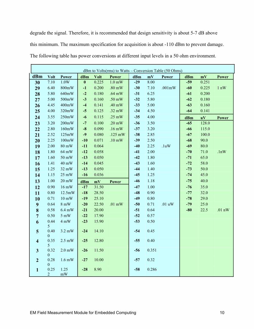
degrade the signal. Therefore, it is recommended that design sensitivity is about 5-7 dB above
this minimum. The maximum specification for acquisition is about -110 dBm to prevent damage.
The following table has power conversions at different input levels in a 50 ohm environment.
dBm to Volts(rms) to Watts – Conversion Table (50 Ohms)dBm Volt Power dBm Volt Power dBm mV Power dBm mV Power
30 7.10 1.0W 0 0.225 1.0 mW -29 8.00 -59 0.251 29 6.40 800mW -1 0.200 .80 mW -30 7.10 .001mW -60 0.225 1 nW28 5.80 640mW -2 0.180 .64 mW -31 6.25 -61 0.200 27 5.00 500mW -3 0.160 .50 mW -32 5.80 -62 0.180 26 4.45 400mW -4 0.141 .40 mW -33 5.00 -63 0.160 25 4.00 320mW -5 0.125 .32 mW -34 4.50 -64 0.141
24 3.55 250mW -6 0.115 .25 mW -35 4.00 dBm uV Power23 3.20 200mW -7 0.100 .20 mW -36 3.50 -65 128.0 22 2.80 160mW -8 0.090 .16 mW -37 3.20 -66 115.0 21 2.52 125mW -9 0.080 .125 mW -38 2.85 -67 100.0 20 2.25 100mW -10 0.071 .10 mW -39 2.50 -68 90.0 19 2.00 80 mW -11 0.064 -40 2.25 .1uW -69 80.0 18 1.80 64 mW -12 0.058 -41 2.00 -70 71.0 .1nW17 1.60 50 mW -13 0.050 -42 1.80 -71 65.0 16 1.41 40 mW -14 0.045 -43 1.60 -72 58.0 15 1.25 32 mW -13 0.050 -44 1.40 -73 50.0 14 1.15 25 mW -16 0.036 -45 1.25 -74 45.0
13 1.00 20 mW dBm mV Power -46 1.18 -75 40.0
12 0.90 16 mW -17 31.50 -47 1.00 -76 35.0 11 0.80 12.5mW -18 28.50 -48 0.90 -77 32.0 10 0.71 10 mW -19 25.10 -49 0.80 -78 29.0 9 0.64 8 mW -20 22.50 .01 mW -50 0.71 .01 uW -79 25.0 8 0.58 6.4 mW -21 20.00 -51 0.64 -80 22.5 .01 nW7 0.50 5 mW -22 17.90 -52 0.57 6 0.44
54 mW -23 15.90 -53 0.50
5 0.40
03.2 mW -24 14.10 -54 0.45
4 0.35
52.5 mW -25 12.80 -55 0.40
3 0.32
02.0 mW -26 11.50 -56 0.351
2 0.28
01.6 mW -27 10.00 -57 0.32
1 0.25
21.25 mW
-28 8.90 -58 0.286
EM Field Measurement Module for Embedded Computing 10

2.2 SpecificationsThe following are the required project specifications. The devised modules must measure
the power intensity in both L1 and L2 band frequencies. Each of the two modules will be
assigned a band with a bandwidth of 25 MHz. Each module must be rugged enough to be used in
the field at normal outdoor temperature ranges.
The power to be measured has a range from -80 dBm to 30 dBm. Note that this range is
much greater that the average operation of GPS receivers (-130 to -110 dBm). This range
corresponds to a range in watts from .01nW to 1W.
The modules are to output power data to an external peripheral device through an RS-232
communication port. A data transfer protocol is defined in Chapter 3.3 Software. Because there
is constant communication with an external device internal data storage is not necessary.
The power supply must operate with 120V/60Hz AC or 12V DC input. Ultimately, the
modules can be powered up from a wall outlet or a car battery.
One main feature that the design must provide is open architecture. Implementation of an
open architecture design allows the user to interchange, upgrade, or modify components to adjust
the module to a different specification. For this project, the implementation of open architecture
must concentrate in a different frequencies, but not a different power range.
Antenna Frequencies: 1227.6MHz and 1575.42MHz
Frequency Bandwidth (-3dB): 25MHz
Input Power Range: -80dBm to 30dBm
Measurement Resolution: 1dB
Sampling Rate: >10 Samples/second
External Communication: RS-232 Serial Port
Onboard Data Storage: Not required
Max PCB Size: 3.775”x3.550”
Voltage Supply: 120V/60Hz AC, 12V DC
Table 1: Specifications
EM Field Measurement Module for Embedded Computing 11

2.3 DeliverablesAt the completion of the project the deliverables include the two modules for L1 and L2
GPS frequencies that meet the stated customer specifications.
Along with the finished modules, a level 1 documentation package is submitted. The
level 1 documentation includes detailed instructions for the reconstruction of identical modules.
For this purpose, it contains hardware part numbers, software source code, as well as user
operation instructions. The documentation also incorporates designer recommendations for
future upgrades or changes.
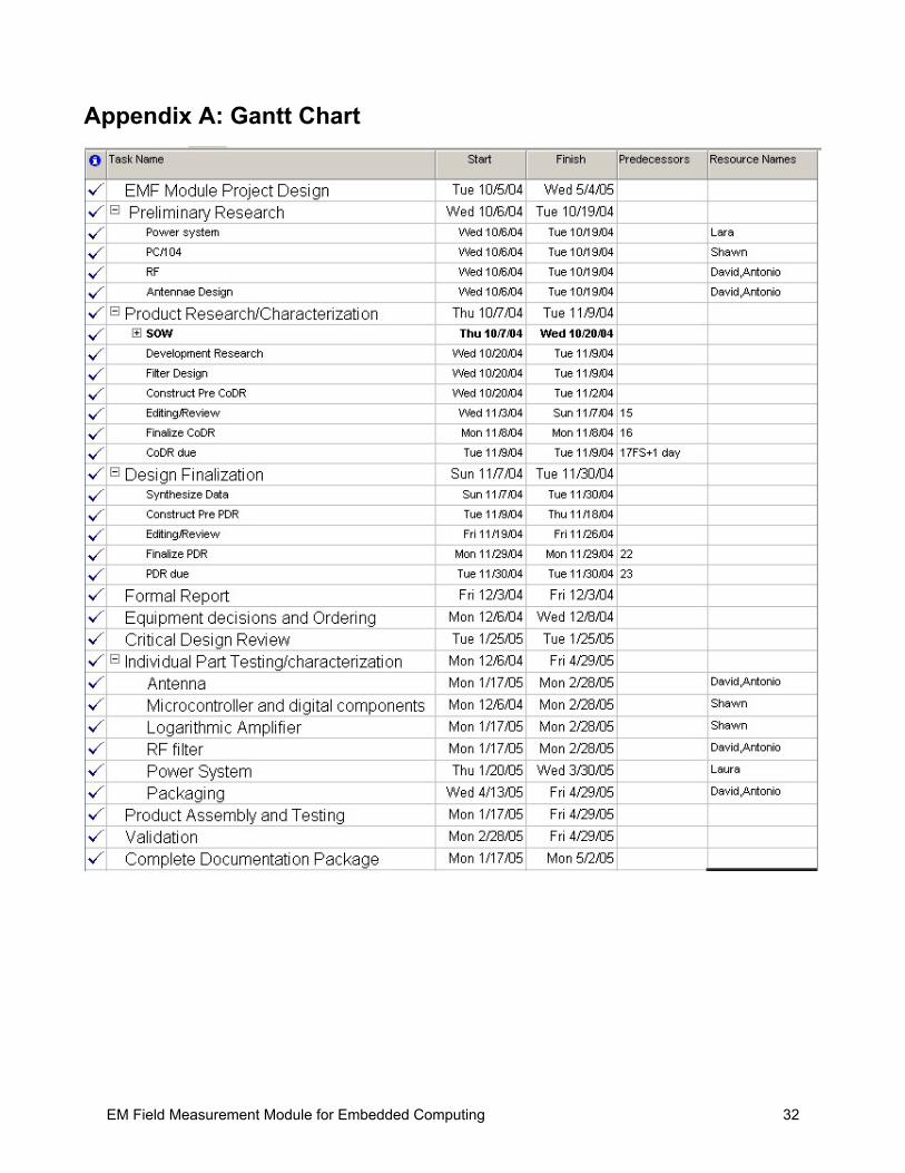
2.4 Project PlanningThis project was quality driven. The amount of time and money available was sufficient
and was recognized to be sufficient from an early stage in the project. This project began on
September 22nd, 2004 and the final modules are being sent to NAWC-WD on May 5th, 2005. It is
being competed on time and under budget. Illustration 1 is the critical path that was followed and
indicated when money was spent.
Illustration 1: Critical Path
EM Field Measurement Module for Embedded Computing 12

2.4.1 BudgetThere was $5400 available to develop these two modules. The final budget only spent
$2654 which is less than half of the available funds. Each additional module should cost about
$1200 in materials.
One of the reasons the budget was kept as low as it is, is due to free samples and
donations from Analog Devices, Maxim, Ztec Instruments, and the NMT EE Department.
Another reason for low expenses is proper planning. The design did not change significantly
after the design was finalized and the purchase orders were sent.
2.4.2 Human Resource ManagementThe project began with some background research and initial design brainstorming. After
the design was finalized and parts were received, there were several parallel paths. Software
development, PCB layout and prototyping, and housing assembly were the three long poles. All
three finished testing at about the same time in late April which allowed for a couple weeks of
final testing, optimization, and bug fixes. See Appendix A for the detailed gantt chart.
Component Unit Price Quantity PriceAntenna 177.50 2 355.00Filter 125.00 3 375.00Attenuator 35.00 4 140.00Amplifier 290.00 2 580.00Signal Splitter 250.00 2 500.00Logarithmic Detector 0.00 4 0.00Microcontroller 6.00 4 24.00RS-232 Converter/Adapter 0.00 2 0.00Power Converters/ Regulators 20.00 2 40.00Packaging 70.00 2 140.00Miscellaneous 500.00 1 500.00Total 2654.00Available 5400.00
Table 2: Budget
EM Field Measurement Module for Embedded Computing 13
Chapter 3: Project Design
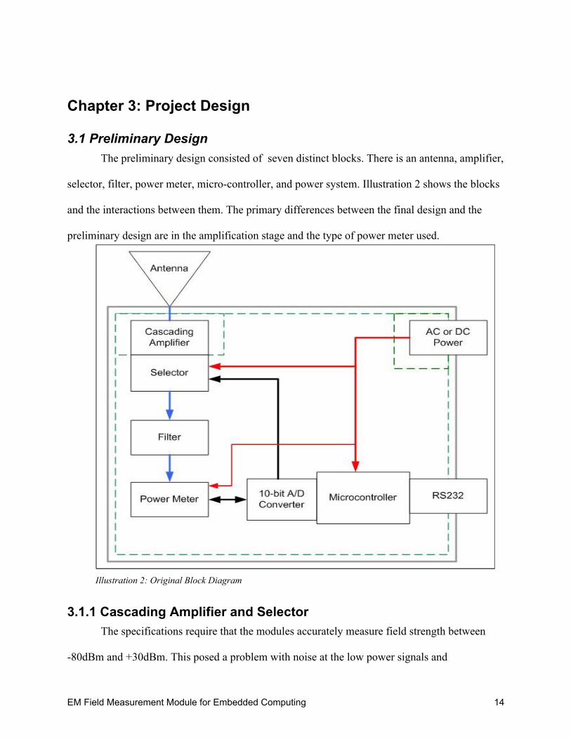
3.1 Preliminary DesignThe preliminary design consisted of seven distinct blocks. There is an antenna, amplifier,
selector, filter, power meter, micro-controller, and power system. Illustration 2 shows the blocks
and the interactions between them. The primary differences between the final design and the
preliminary design are in the amplification stage and the type of power meter used.
3.1.1 Cascading Amplifier and SelectorThe specifications require that the modules accurately measure field strength between
-80dBm and +30dBm. This posed a problem with noise at the low power signals and
Illustration 2: Original Block Diagram
EM Field Measurement Module for Embedded Computing 14
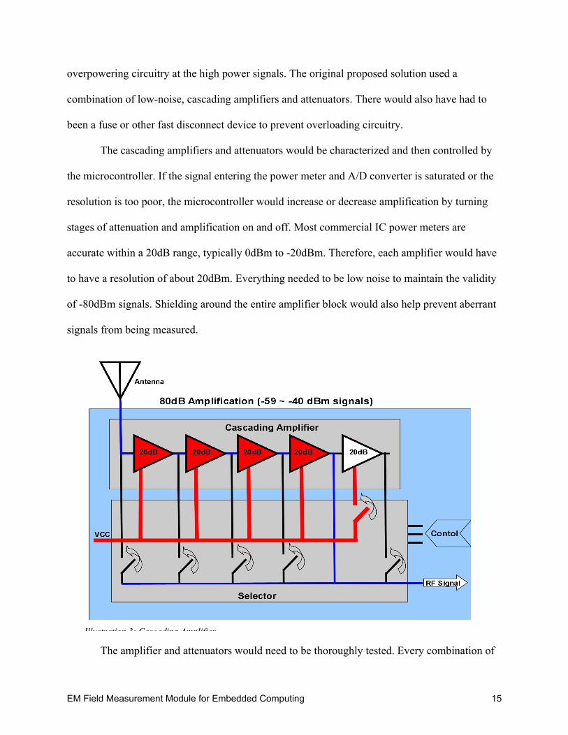
overpowering circuitry at the high power signals. The original proposed solution used a
combination of low-noise, cascading amplifiers and attenuators. There would also have had to
been a fuse or other fast disconnect device to prevent overloading circuitry.
The cascading amplifiers and attenuators would be characterized and then controlled by
the microcontroller. If the signal entering the power meter and A/D converter is saturated or the
resolution is too poor, the microcontroller would increase or decrease amplification by turning
stages of attenuation and amplification on and off. Most commercial IC power meters are
accurate within a 20dB range, typically 0dBm to -20dBm. Therefore, each amplifier would have
to have a resolution of about 20dBm. Everything needed to be low noise to maintain the validity
of -80dBm signals. Shielding around the entire amplifier block would also help prevent aberrant
signals from being measured.
The amplifier and attenuators would need to be thoroughly tested. Every combination of
Illustration 3: Cascading Amplifier
EM Field Measurement Module for Embedded Computing 15

amplification and attenuation must be tested for noise, insertion loss, VSWR, and actual
amplification. A combination of spectrum analyzers, function generators, and oscilloscopes will
be able to do this testing and calibration
The selector was a combination of RF and power switching devices. It must accept the
control signals from the microcontroller, power the appropriate amplifiers, and forward the
correct amplified RF output. Illustration 3 is an example of what would happen when measuring
a -50dBm signal. The microcontroller would send the signal for 80dB amplification and the
selector would forward the fourth amplifier's output.
This design could theoretically work, but was plagued with noise issues. Each amplifier
would generate noise when powered, so when receiving a low power signal, all the stages of
amplification would be turned on. This noise could have potentially been amplified enough to
drown out the signal being measured. Another issue with this design was the open architecture
spec. In order to change the power detection range, stages of amplification would have to be
added or removed, or the amount of amplification on each stage would have to vary. The cascade
of amplifiers would have been a line of IC’s, thus switching them out or adding/removing stages
of amplification could not be done easily.
3.1.2 Power MeterThe original design for the power detector was a rectifier and peak detector designed out
of discrete components. This idea had a few problems including noise, switching times,
reliability, and low power range. The long circuit wires and distances between components
resulted in large noise issues. The requirement to reset the peak detector required more
connections to the microcontroller and a more complicated software routine to get data from the
detector. A professionally made IC is a much better choice.
EM Field Measurement Module for Embedded Computing 16

There are several companies that make an IC capable of converting an RF signal into a
DC voltage. They all seem to have about the same limitations. They operate between 3 and 5
volts and have very low current draw. The output is typically an analog DC signal between 0
volts and the operating voltage. The hardest part to deal with is the input has to be between
specific values (e.g. 0 and 20 dBm) which is why the amplifier, selector, and filter setup were so
complicated.
3.2 Present DesignThe final design is broken down into the RF front end, the analog and digital
components, software and the enclosure. A simple block diagram is shown in Illustration 4. The
Illustration 4: Final Block Diagram
EM Field Measurement Module for Embedded Computing 17

blue lines indicate the path of the RF signal. The signal is captured by the antenna and filtered. It
is then split and sent through two channels, one for amplification and the other for attenuation.
Logarithmic detectors convert the two channels power values into voltages the microcontroller
can use to determine the EM field strength. The green solid lines represent DC voltages and DC
signals. The red lines indicate power, and the green dashed box is shielding that surrounds the
entire enclosure. The entire box is shielded to prevent external noise from affecting the circuitry
and also to prevent internal circuitry from affecting the antenna reception.
3.2.1 RF Front End DesignThe RF front end is composed of the antenna, filtering, a signal splitter, amplification and
attenuation, and logarithmic detectors interfacing to the microcontroller.
Since two modules are going to be constructed, two separate antennas were ordered. One
antenna is strictly L1 and the other is a dual band L1/L2 antenna. Both of them are 50ohm
antennas The antennas are passive, so have approximately zero gain. The passive antennas are
chosen because the output voltage from an antenna receiving a +30dBm signal is about 7V. If
the antenna were to amplify that by 20dB, the output voltage would be about 70V. It is easy
enough to acquire components that can handle 7V but 70V is nearly impossible. The antennas
use a standard connector type, SMA, to facilitate interchangeability and noise reduction. The L1
antenna’s reflection pattern, as shown in Illustration 8, shows it have a clean bandpass filter
design centered around 1.57542 GHz. This is exactly as expected and desired, so only a single
GPS L1 filter was required in the L1 module. The L2 module’s antenna is a dual band antenna,
and its reflection pattern is far from ideal or desired, as shown in Illustration 7. If only a single
GPS L2 filter is used in the L2 module, only 20dBm of frequency isolation is achieved. To
increase our isolation and our accuracy, an extra GPS filter is added in line between the antenna
EM Field Measurement Module for Embedded Computing 18

and the signal splitter. This allowed for an acceptable value of 40dBm of frequency isolation.
Next the signal is sent into a GPS splitter, to create two channels so the power detection
range of –80dBm to +30dBm is possible. The logarithmic detectors used (Analog Device's
AD8313) have detection ranges roughly from –65dBm to 5dBm at frequencies being measured.
This is slightly smaller than the specification range. So two channels are created, one channel
going through a amplifier of 30dBm and the other channel through a 30dBm attenuation. The
attenuator is a passive device and is simply connected in-line through its SMA connector. The
amplifier is a active device that requires power through a bias-tee. The bias-tee has two inputs
and one output, all SMA connections. One input is the RF signal from the splitter, and the other
is 3.3V DC power. The output is a combination of RF and DC, sent into the input of the
amplifier. Thus the amplified channel will be able to detect measured field strength values
ranging roughly from –100dBm to –20dBm, and the attenuated channel will be able to detect
field strength values ranging roughly from -40dBm to +40dBm. Using the two channels
dynamically will give power range needed.
The logarithmic detectors output a voltage range from 0.7V to 1.7V varying linearly with
the power coming into the device. See Illustration 14 for actual results. Comparing the voltage
out of the logarithmic detectors with a calibrated look up table, the microcontroller will be able
to discern which channel is valid, and output the correct data through the RS-232 port. This
process will be described later in the software section.
3.2.2 Analog and Digital DesignThere are three main components to the analog and digital portion of these modules: the
microcontroller, the RS-232 converter, and the power regulators. Appendix C has the final PCB
layout which shows all the connections and requirements.
EM Field Measurement Module for Embedded Computing 19
The microcontroller used is a PIC18F1320. Although the 1320 has 18 pins, this design
only requires seven of them. Two pins are used for 3.3V and Ground (pins 5 and 14), a second
pair of pins is used for transmitting and receiving RS-232 data (pins 9 and 10), another two pins
are used as analog inputs to the on-chip analog to digital converters (pins 1 and 2), and the final
pin is used as a digital control line for the amplifier's power switch (pin 3). If future designs
require additional sampling channels pins 6 through 8 can be used as additional ADCs.
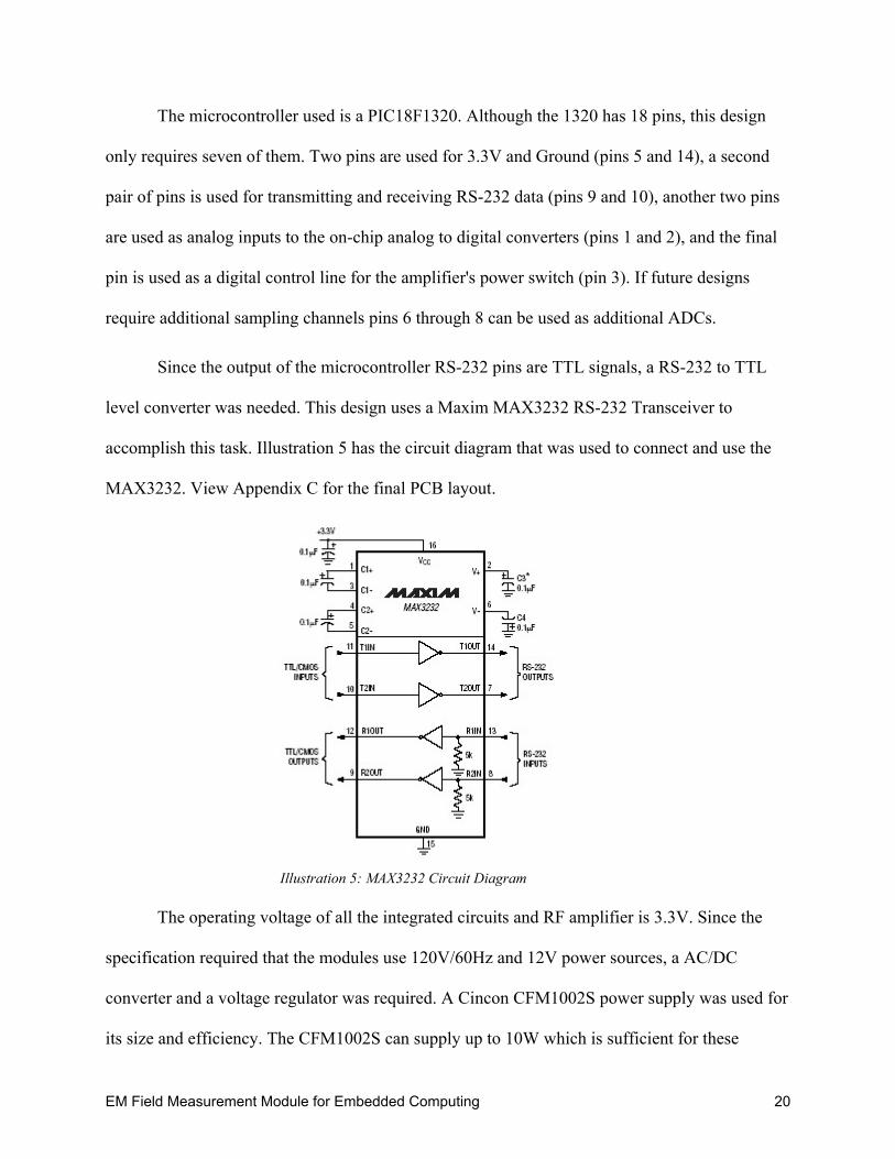
Since the output of the microcontroller RS-232 pins are TTL signals, a RS-232 to TTL
level converter was needed. This design uses a Maxim MAX3232 RS-232 Transceiver to
accomplish this task. Illustration 5 has the circuit diagram that was used to connect and use the
MAX3232. View Appendix C for the final PCB layout.
The operating voltage of all the integrated circuits and RF amplifier is 3.3V. Since the
specification required that the modules use 120V/60Hz and 12V power sources, a AC/DC
converter and a voltage regulator was required. A Cincon CFM1002S power supply was used for
its size and efficiency. The CFM1002S can supply up to 10W which is sufficient for these
Illustration 5: MAX3232 Circuit Diagram
EM Field Measurement Module for Embedded Computing 20
modules. In order to prevent damage to the PCB, ICs, and power supplies, two diodes are used to
separate the dual power source options. In the event that both sources are plugged in, the diodes
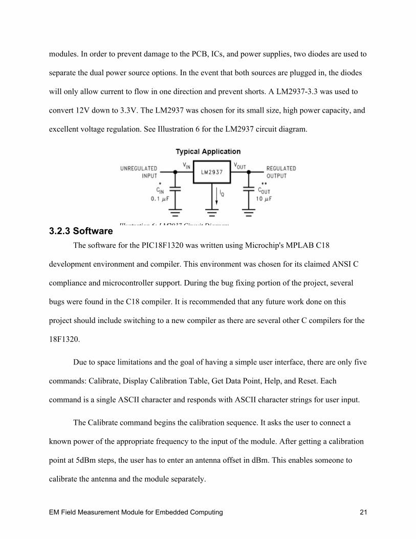
will only allow current to flow in one direction and prevent shorts. A LM2937-3.3 was used to
convert 12V down to 3.3V. The LM2937 was chosen for its small size, high power capacity, and
excellent voltage regulation. See Illustration 6 for the LM2937 circuit diagram.
3.2.3 SoftwareThe software for the PIC18F1320 was written using Microchip's MPLAB C18
development environment and compiler. This environment was chosen for its claimed ANSI C
compliance and microcontroller support. During the bug fixing portion of the project, several
bugs were found in the C18 compiler. It is recommended that any future work done on this
project should include switching to a new compiler as there are several other C compilers for the
18F1320.
Due to space limitations and the goal of having a simple user interface, there are only five
commands: Calibrate, Display Calibration Table, Get Data Point, Help, and Reset. Each
command is a single ASCII character and responds with ASCII character strings for user input.
The Calibrate command begins the calibration sequence. It asks the user to connect a
known power of the appropriate frequency to the input of the module. After getting a calibration
point at 5dBm steps, the user has to enter an antenna offset in dBm. This enables someone to
calibrate the antenna and the module separately.
Illustration 6: LM2937 Circuit Diagram
EM Field Measurement Module for Embedded Computing 21
The Display Calibration Table displays all the calibration points from -80dBm to 30dBm
as well as each channel's minimum and maximum accurate measurement. Viewing this helps to
debug any inaccuracies or nonsensical data.
The Get Data Point command polls the ADCs and converts those numbers into a dBm
value which is sent back to the user. The conversion function verifies limits and averages points
if more than one channel has valid data.
The Help command displays the available commands. The Reset command performs a
software restart. This command does not empty any data in EEPROM.
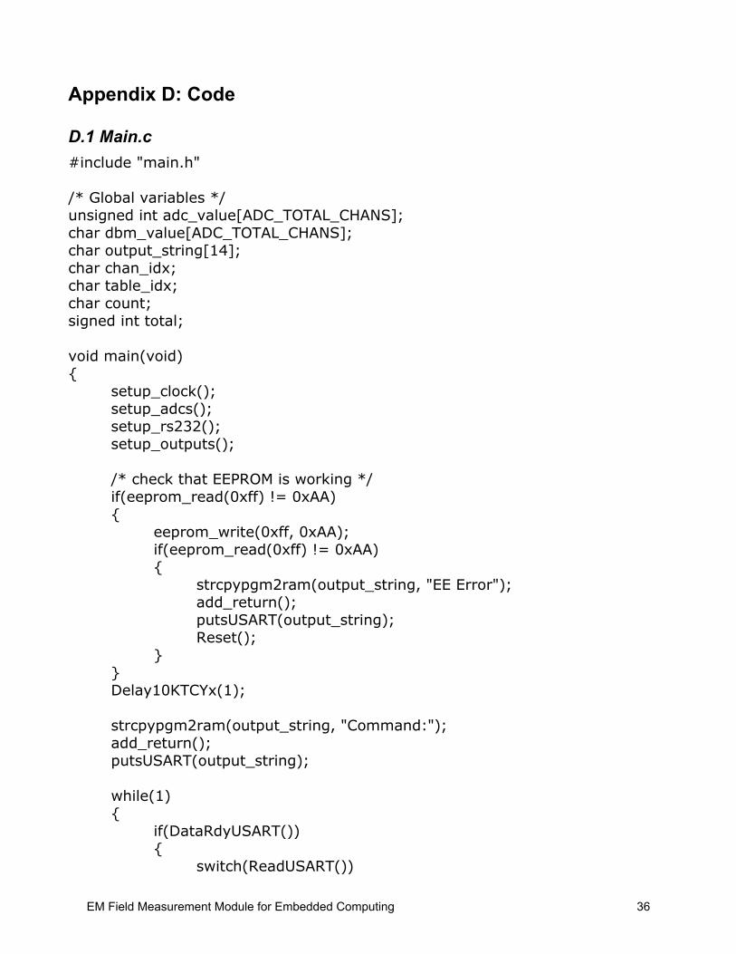
Appendix D has all of the source code. The Level 1 Documentation package has the
project files and compiled code.
3.2.4 EnclosureFor the enclosure, the size of the components, along with the connecting cables and the
different schemes the parts could be laid out in, were considered. The final setup has the GPS
filter on ½” aluminum standoffs, with the splitter stacked above it. In the L2 module there is the
added filter stacked in the middle. This stack is located on one end of the enclosure base. The
PCB board is located on the opposite end, with the power supply facing upwards for ease of
connecting the RF components to the SMA jacks on the board. The PCB is supported by four 2”
aluminum standoffs. Running on one side between the filter/splitter stack and the PCB is the
bias-tee and the attached amplifier. The amplifier is also held up by ½” aluminum standoffs.
Running along the other side is the attenuated line to the PCB.
Three main materials were considered for the construction of the enclosure that are easily
accessible, inexpensive, and maneuverable: Those are steel sheet, aluminum alloy sheet, and
EM Field Measurement Module for Embedded Computing 22

polymer based materials. Because the module deals with low power signals, shielding is
important to prevent interference into internal components from external sources. Steel and
aluminum are good conductors, thus providing good shielding. In the other hand, polymer or
plastic materials collect static charge which is harmful to sensitive internal components.
The enclosure is designed to have multiple bends and holes. Some factors that need to be
considered is the material tensile strength and ductility. Steel has a higher tensile strength which
consequentially makes it more brittle. Aluminum in the other hand, is more ductile and can
experience greater deformation without fracture. Other benefits of aluminum is weight, and
corrosion resistance. Therefore, an aluminum alloy sheet was selected for the construction of the
enclosure.
The sheet used for the base (See Appendix B) is 16”x11”. The 5”x11” sections (marked
off with a dashed line) on the left and right sides of the sheet would become walls of the base.
The center 6”x11” section would become the bottom of the module. Straight through, non-
threaded holes were drilled as indicated in the center base to connect the standoffs to support the
various components. On the right wall section holes for the DC power jack(3/8” diameter), the
fuse (1/2” diameter) and a cut out rectangle (3/4” by 1”) to hold the AC power jack were made.
On the left wall section, a standard DB9 connector punch was used to make the hole for the RS-
232 serial connection. Four, size 6-32 tapped holes are drilled on each wall as indicated on the
diagram, to secure the top to the base. If a courser thread type is desired, a thicker sheet would
need to be used to ensure that the bolts have enough thread to bite into.
The sheet used for the top (see Appendix B) is 21.2”x7.25”. On the top and bottom of the
sheet, 5” in from the left and right side, four isosceles right triangles are cut out. This is to allow
for the bend in each flap. Next eight holes are drilled, four in the top and four in the bottom as
EM Field Measurement Module for Embedded Computing 23

shown. The holes are straight through, non-threaded and have a diameter near .2”, large enough
to allow the #6-32 screws without passing the head. Another hole is drilled on one end of what
will become the top, with a diameter of ¼”. This will accept a female SMA connector type,
which can be secured from the outside, and will hold the modules antenna. All along the top and
bottom of the sheet, a line ½” from the edge is made. A 90 degree bend is made along both these
lines, creating securing lips for the lid. Two more 90 bends are made along lines connecting the
cut-out triangles along the 5” line as shown in the diagram.
To protect the internal circuitry from external noise, and also the antenna from internal
noise, 90 dBm shielding is lined inside the lid and the base. Then the individual components can
be placed inside, and the module top and bottom be fit together and secured with #6-32 bolts.
EM Field Measurement Module for Embedded Computing 24
Chapter 4: Results
4.1 Subsystem SpecificationsEach component in the RF front ends were checked before being used in a larger
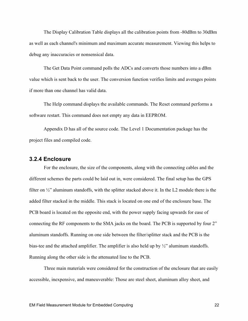
subsystem to verify operation. Illustration 8 has the L1 antenna reflection pattern. It indicates
that the antenna picks up L1 signals very well and almost nothing else. On the other hand,
Illustration 7 has the L1/L2 antenna reflection pattern which indicates that the antenna picks up
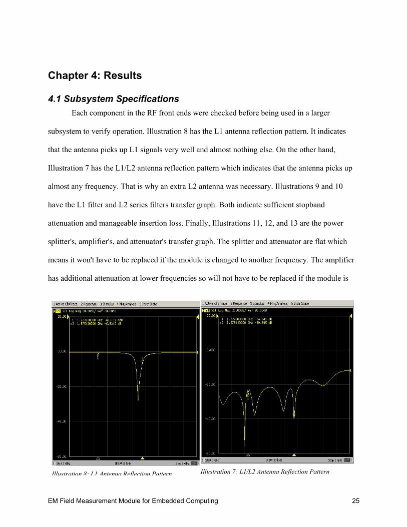
almost any frequency. That is why an extra L2 antenna was necessary. Illustrations 9 and 10
have the L1 filter and L2 series filters transfer graph. Both indicate sufficient stopband
attenuation and manageable insertion loss. Finally, Illustrations 11, 12, and 13 are the power
splitter's, amplifier's, and attenuator's transfer graph. The splitter and attenuator are flat which
means it won't have to be replaced if the module is changed to another frequency. The amplifier
has additional attenuation at lower frequencies so will not have to be replaced if the module is
Illustration 8: L1 Antenna Reflection Pattern Illustration 7: L1/L2 Antenna Reflection Pattern
EM Field Measurement Module for Embedded Computing 25
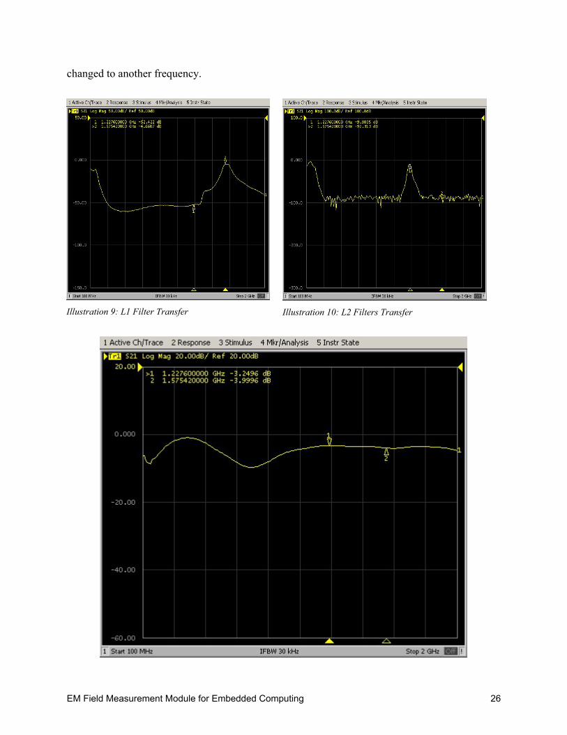
changed to another frequency.
Illustration 9: L1 Filter Transfer Illustration 10: L2 Filters Transfer
EM Field Measurement Module for Embedded Computing 26
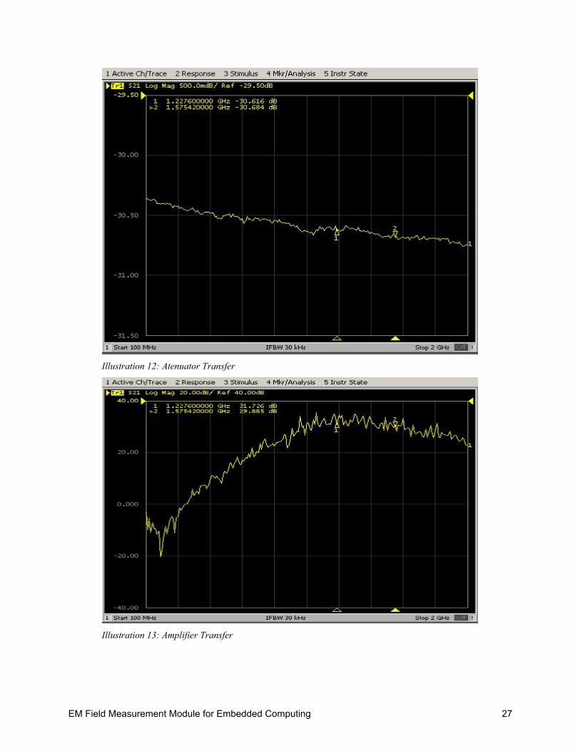
Illustration 12: Atenuator Transfer
Illustration 13: Amplifier Transfer
EM Field Measurement Module for Embedded Computing 27
4.2 Reliability
4.2.1 Mean Time Between FailuresMTBF is a predicting tool measured in hours, which indicates the sturdiness of the device
– the average time the device will function before breakdown based on collective testing by
manufacturer. The calculation is defined by the following formula:
MTBF = Total Hours of Operation/Outage Frequency
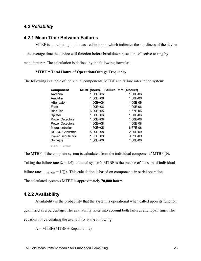
The following is a table of individual components' MTBF and failure rates in the system:
The MTBF of the complete system is calculated from the individual components' MTBF (θ).
Taking the failure rate (λ = 1/θ), the total system's MTBF is the inverse of the sum of individual
failure rates: MTBF total = 1/∑λ. This calculation is based on components in serial operation.
The calculated system's MTBF is approximately 70,000 hours.
4.2.2 AvailabilityAvailability is the probability that the system is operational when called upon its function
quantified as a percentage. The availability takes into account both failures and repair time. The
equation for calculating the availability is the following:
A = MTBF/(MTBF + Repair Time)
Component MTBF (hours) Failure Rate (1/hours)Antenna 1.00E+06 1.00E-06Amplifier 1.00E+06 1.00E-06Attenuator 1.00E+06 1.00E-06Filter 1.00E+06 1.00E-06Bias Tee 6.00E+05 1.67E-06Splitter 1.00E+06 1.00E-06Power Detectors 1.00E+08 1.00E-08Power Detectors 1.00E+08 1.00E-08Microcontroller 1.50E+05 6.67E-06RS-232 Converter 5.00E+08 2.00E-09Power Regulators 1.05E+08 9.52E-09Software 1.00E+06 1.00E-06
Table 3: MTBF
EM Field Measurement Module for Embedded Computing 28
The repair time of each component in the module has an average of 24 hours. This includes
replacement of components and calibration of power values in the micro-controller. The total
availability of the system takes in account the total MTBF with the repair time of each
component:
A = (70,000/(70,000 + 24)) x100% = 99.966%
4.3 System SpecificationsThe final modules almost meet all of the specifications. The only specification that was
not completely met is the power range. Instead of -80 to 30 dBm, the modules have only been
successfully tested from -75dBm to 15dBm. Part of the untested region is due to lack of
equipment. The available test equipment was only accurate up to 15 dBm.
After assembling the modules and calibrating the look-up table, the illustration 14 was
compiled. This graph shows that the module has distinct, repeatable outputs for the entire input
range. The third (orange dotted) line is the attenuated channel output before the microcontroller
controlled power switch was added.
Illustration 14: ADC Output vs. dBm
EM Field Measurement Module for Embedded Computing 29

Chapter 5: ConclusionThe modules are completely operational. The final modules meet the specifications very
closely. Most of the challenges that emerged in the process originated mostly from design issues, which
were addressed after multiple revisions. Other technical issues allowed the team to understand topics
that are associated with RF type design such as noise, calibration issues, and data processing. However,
there are several suggestions for future improvement of the module design and operation.
For the microcontroller and software, it is advisable to have ample memory and a compiler that
optimizes the code based on the specific processor. Any future work done on this project should
include a switch to a new compiler and/or a microcontroller with additional data memory.
Because some noise leakage was experienced between channels, a switching device was
implemented later in the project to solve the problem. However, this problem could be avoided in the
PCB layout design. The attenuated, amplified, and power channels must be separated as much as
possible to prevent any leakage between channels. Along with shielding, this approach saves
computation for the processor. It also allows for an easily scalable design because the software
wouldn't need to know which channel is amplified.
Development management is very important for the success of the project. Some challenges
included coordination of tasks. Although the distribution of tasks was intended to be equal, the
completion times were not foreseen. A suitable strategy is to maintain a balanced distribution of tasks,
and alternative parallel approaches in case of premature or prolonged completion of assignments. This
can be achieved by maintaining logs and inter-team progress reports.
EM Field Measurement Module for Embedded Computing 30

Chapter 6: ReferencesBethune, James D. Engineering Graphics with AutoCAD. Prentice-Hall Inc. 1995.
Callister, Jr. William D. Materials Science and Engineering An Introduction, 5th Ed. John Wiley and Sons Inc. 2000.
Carr, Joseph J. Elements of Electronic Instrumentation and Measurement, 2nd Ed. Prentice-Hall Inc. 1986.
Dana, Peter H. (2005, May 4). Code Phase Tracking (Navigation). [WWW] URLhttp://www.colorado.edu/geography/gcraft/notes/gps/gps.html.
GPS World. (2005, May 4) GPS Reference [WWW] URL http://www.gpsworld.com/gpsworld/static/staticHtml.jsp?id=7860.
Hill, Winfield and Paul Horowitz. The Art of Electronics, 2nd Ed. Cambridge University Press. 1989.
Iskander, Magdy F. Electromagnetic Field and Waves. Waveland Press Inc. 1992.
Kernighan, Brian W. and Dennis Ritchie. C Programming Language, 2nd Ed. Prentice-Hall PTR. 1988.
Neamen, Donald A. Electronic Circuit Analysis and Design. Times Mirror Higher Education Group Inc. 1996.
Sedra, Adel and KC Smith. Microelectronic Circuits, 4th Ed. Oxford University Press. 1998.
Smith, Richard F.M. And Stanley Wolf. Student Manual: Electronic Instrumentation Laboratories, 2nd Ed. Pearson Education Inc 2004.
Wikipedia. (2005, May 4) dBm [WWW] URL http://en.wikipedia.org/wiki/DBm.
Wikipedia. (2005, May 4) Global Positioning System [WWW] URL http://en.wikipedia.org/wiki/GPS.
EM Field Measurement Module for Embedded Computing 31
Appendix A: Gantt Chart
EM Field Measurement Module for Embedded Computing 32

EM Field Measurement Module for Embedded Computing 33

Appendix B: Module Housing
EM Field Measurement Module for Embedded Computing 34

Appendix C: PCB
EM Field Measurement Module for Embedded Computing 35
Appendix D: Code
D.1 Main.c#include "main.h"
/* Global variables */unsigned int adc_value[ADC_TOTAL_CHANS];char dbm_value[ADC_TOTAL_CHANS];char output_string[14];char chan_idx;char table_idx;char count;signed int total;
void main(void){
setup_clock();setup_adcs();setup_rs232();setup_outputs();
/* check that EEPROM is working */if(eeprom_read(0xff) != 0xAA){
eeprom_write(0xff, 0xAA);if(eeprom_read(0xff) != 0xAA){
strcpypgm2ram(output_string, "EE Error"); add_return();putsUSART(output_string);Reset();
}}Delay10KTCYx(1);
strcpypgm2ram(output_string, "Command:"); add_return();putsUSART(output_string);
while(1){
if(DataRdyUSART()){
switch(ReadUSART())
EM Field Measurement Module for Embedded Computing 36
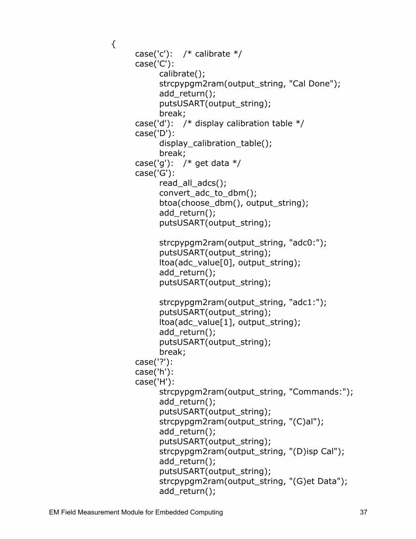
{case('c'): /* calibrate */case('C'):
calibrate();strcpypgm2ram(output_string, "Cal Done");add_return();putsUSART(output_string);break;
case('d'): /* display calibration table */case('D'):
display_calibration_table();break;
case('g'): /* get data */case('G'):
read_all_adcs();convert_adc_to_dbm();btoa(choose_dbm(), output_string); add_return();putsUSART(output_string);
strcpypgm2ram(output_string, "adc0:");putsUSART(output_string);ltoa(adc_value[0], output_string);add_return();putsUSART(output_string);
strcpypgm2ram(output_string, "adc1:");putsUSART(output_string);ltoa(adc_value[1], output_string);add_return();putsUSART(output_string);break;
case('?'):case('h'):case('H'):
strcpypgm2ram(output_string, "Commands:");add_return();putsUSART(output_string);strcpypgm2ram(output_string, "(C)al");add_return();putsUSART(output_string);strcpypgm2ram(output_string, "(D)isp Cal");add_return();putsUSART(output_string);strcpypgm2ram(output_string, "(G)et Data");add_return();
EM Field Measurement Module for Embedded Computing 37
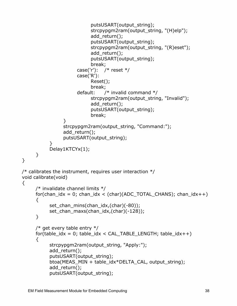
putsUSART(output_string);strcpypgm2ram(output_string, "(H)elp");add_return();putsUSART(output_string);strcpypgm2ram(output_string, "(R)eset");add_return();putsUSART(output_string);break;
case('r'): /* reset */case('R'):
Reset();break;
default: /* invalid command */strcpypgm2ram(output_string, "Invalid");add_return();putsUSART(output_string);break;
}strcpypgm2ram(output_string, "Command:");add_return();putsUSART(output_string);
}Delay1KTCYx(1);
}}
/* calibrates the instrument, requires user interaction */void calibrate(void){
/* invalidate channel limits */for(chan_idx = 0; chan_idx < (char)(ADC_TOTAL_CHANS); chan_idx++){
set_chan_mins(chan_idx,(char)(-80));set_chan_maxs(chan_idx,(char)(-128));
}
/* get every table entry */for(table_idx = 0; table_idx < CAL_TABLE_LENGTH; table_idx++){
strcpypgm2ram(output_string, "Apply:");add_return();putsUSART(output_string);btoa(MEAS_MIN + table_idx*DELTA_CAL, output_string);add_return();putsUSART(output_string);
EM Field Measurement Module for Embedded Computing 38
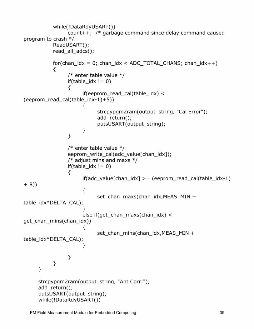
while(!DataRdyUSART())count++; /* garbage command since delay command caused
program to crash */ReadUSART(); read_all_adcs();
for(chan_idx = 0; chan_idx < ADC_TOTAL_CHANS; chan_idx++){
/* enter table value */if(table_idx != 0){
if(eeprom_read_cal(table_idx) < (eeprom_read_cal(table_idx-1)+5))
{strcpypgm2ram(output_string, "Cal Error"); add_return();putsUSART(output_string);
}}
/* enter table value */eeprom_write_cal(adc_value[chan_idx]);/* adjust mins and maxs */if(table_idx != 0){
if(adc_value[chan_idx] >= (eeprom_read_cal(table_idx-1) + 8))
{set_chan_maxs(chan_idx,MEAS_MIN +
table_idx*DELTA_CAL);}else if(get_chan_maxs(chan_idx) <
get_chan_mins(chan_idx)){
set_chan_mins(chan_idx,MEAS_MIN + table_idx*DELTA_CAL);
}
}}
}
strcpypgm2ram(output_string, "Ant Corr:"); add_return();putsUSART(output_string);while(!DataRdyUSART())
EM Field Measurement Module for Embedded Computing 39
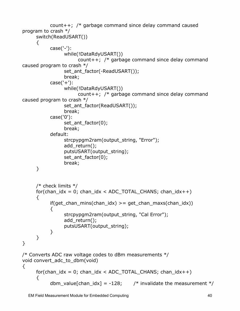
count++; /* garbage command since delay command caused program to crash */
switch(ReadUSART()){
case('-'):while(!DataRdyUSART())
count++; /* garbage command since delay command caused program to crash */
set_ant_factor(-ReadUSART());break;
case('+'):while(!DataRdyUSART())
count++; /* garbage command since delay command caused program to crash */
set_ant_factor(ReadUSART());break;
case('0'):set_ant_factor(0);break;
default:strcpypgm2ram(output_string, "Error"); add_return();putsUSART(output_string);set_ant_factor(0);break;
}
/* check limits */for(chan_idx = 0; chan_idx < ADC_TOTAL_CHANS; chan_idx++){
if(get_chan_mins(chan_idx) >= get_chan_maxs(chan_idx)){
strcpypgm2ram(output_string, "Cal Error"); add_return();putsUSART(output_string);
}}
}
/* Converts ADC raw voltage codes to dBm measurements */void convert_adc_to_dbm(void){
for(chan_idx = 0; chan_idx < ADC_TOTAL_CHANS; chan_idx++){
dbm_value[chan_idx] = -128; /* invalidate the measurement */
EM Field Measurement Module for Embedded Computing 40

for(table_idx = 1; table_idx < CAL_TABLE_LENGTH; table_idx++)/* go through all entries */
{if((eeprom_read_cal(table_idx) >= adc_value[chan_idx]) &&
(eeprom_read_cal(table_idx - 1) <= adc_value[chan_idx])) /* if there is a valid point */
{ /* calculate the dbm value */dbm_value[chan_idx] = MEAS_MIN +
(DELTA_CAL*(table_idx-1)) +
(((DELTA_CAL*(adc_value[chan_idx] - eeprom_read_cal(table_idx - 1)))+
(eeprom_read_cal(table_idx) - eeprom_read_cal(table_idx - 1))/2 )/
(eeprom_read_cal(table_idx) - eeprom_read_cal(table_idx - 1)) ); }
}}
}
/* selects the valid dBm measurement from an array of possibilities */char choose_dbm(void){
count = 0;total = 0;for(chan_idx = 0; chan_idx < ADC_TOTAL_CHANS; chan_idx++){
if((dbm_value[chan_idx] >= get_chan_mins(chan_idx)) && (dbm_value[chan_idx] <= get_chan_maxs(chan_idx)))
{count++;total += (signed int)dbm_value[chan_idx];
} }
if(count == 0)return -128;
elsereturn ((char)(total/count)+get_ant_factor());
}
/* writes one cal table entry to eeprom */void eeprom_write_cal(unsigned int data){
eeprom_write(sizeof(int)*(CAL_TABLE_LENGTH*chan_idx + table_idx), (unsigned char)(data>>8));
EM Field Measurement Module for Embedded Computing 41
eeprom_write(sizeof(int)*(CAL_TABLE_LENGTH*chan_idx + table_idx)+1, (unsigned char)(data&0x00ff));}
/* writes one byte to EEPROM memory */void eeprom_write(unsigned char address, unsigned char data){
EEADR = address;EEDATA = data;EECON1 &= 0x7f; /* set to eeprom data*/EECON1 |= 0x04; /* enable writes */EECON2 = 0x55; /* required sequence to write */EECON2 = 0xAA;EECON1 |= 0x02; /* start write */
while((unsigned char)(EECON1 & 0x02) == (unsigned char)(0x02)){
Delay1TCY(); /* Delay */}EECON1 &= (0xFF - 0x04);
}
/* reads one cal table entry from eeprom */unsigned int eeprom_read_cal(char entry){
return (((unsigned int)eeprom_read(sizeof(int)*(CAL_TABLE_LENGTH*chan_idx + entry))<<8) +
((unsigned int)eeprom_read(sizeof(int)*(CAL_TABLE_LENGTH*chan_idx + entry)+1)&0x00FF));}
/* reads and returns one byte of eeprom memory */char eeprom_read(unsigned char address){
EEADR = address;EECON1 &= 0x7f; /* set to eeprom data*/EECON1 |= 0x01; /* start read*/
return EEDATA;}
/* configures the RS232 port for 9600 baud */void setup_rs232(void){
baudUSART((unsigned char)(BAUD_IDLE_CLK_HIGH & BAUD_16_BIT_RATE
EM Field Measurement Module for Embedded Computing 42

& BAUD_WAKEUP_OFF & BAUD_AUTO_OFF));OpenUSART((unsigned char)(USART_TX_INT_OFF & USART_RX_INT_OFF &
USART_BRGH_HIGH & USART_CONT_RX & USART_SYNC_SLAVE &
USART_EIGHT_BIT & USART_ASYNCH_MODE), 207);return;
}
/* reads all the ADC values */void read_all_adcs(void){
amplifier_on();Delay1KTCYx(250);ADCON0 &= 0xE3;total = 0;for(count = 0; count < 20; count++){
ConvertADC();while((char)(ADCON0 & 0x02) == (char)0x02);total += ReadADC();
}adc_value[0] = (unsigned int)((unsigned int)total/(unsigned int)count);
amplifier_off();Delay1KTCYx(250);ADCON0 = (ADCON0 & 0xE3) | (0x04);total = 0;for(count = 0; count < 20; count++){
ConvertADC();while((char)(ADCON0 & 0x02) == (char)0x02);total += ReadADC();
}adc_value[1] = (unsigned int)((unsigned int)total/(unsigned int)count);
return;}
/* adds a carriage return and line feed to the end of a string */void add_return(void){
count = strlen(output_string);output_string[count++] = 0x0D;output_string[count++] = 0x0A;output_string[count] = 0;return;
EM Field Measurement Module for Embedded Computing 43

}
/* this function outputs the entire calibration table */void display_calibration_table(void){
for(chan_idx = 0; chan_idx < ADC_TOTAL_CHANS; chan_idx++){
strcpypgm2ram(output_string, "Chan");putsUSART(output_string);btoa(chan_idx, output_string);putsUSART(output_string);strcpypgm2ram(output_string, ":");add_return();putsUSART(output_string);
for(table_idx = 0; table_idx < CAL_TABLE_LENGTH; table_idx++){
itoa(eeprom_read_cal(table_idx),output_string);add_return();putsUSART(output_string);
}strcpypgm2ram(output_string, "min:");putsUSART(output_string);btoa(get_chan_mins(chan_idx), output_string);add_return();putsUSART(output_string);strcpypgm2ram(output_string, "max:");putsUSART(output_string);btoa(get_chan_maxs(chan_idx), output_string);add_return();putsUSART(output_string);
}}
D.2 Main.h#include <p18f1320.h>#include <adc.h>#include <usart.h>#include <stdlib.h>#include <delays.h>#include <string.h>
#define ADC_TOTAL_CHANS 2#define MEAS_MIN -80#define MEAS_MAX 30#define DELTA_CAL 5
EM Field Measurement Module for Embedded Computing 44

#define CAL_TABLE_LENGTH (1 + ((MEAS_MAX - MEAS_MIN) / DELTA_CAL))
#define setup_clock() OSCCON=0x7F,OSCTUNE=0#define setup_adcs() ADCON0=0x01,ADCON1=0x7C,ADCON2=0xBE#define setup_outputs() TRISA=0xEF,LATA=0x10#define amplifier_on() LATA=0x00#define amplifier_off() LATA=0x10#define get_chan_mins(x) eeprom_read(0xF0+ADC_TOTAL_CHANS*x)#define get_chan_maxs(x) eeprom_read(0xF1+ADC_TOTAL_CHANS*x)#define set_chan_mins(x,y) eeprom_write(0xF0+ADC_TOTAL_CHANS*x,y)#define set_chan_maxs(x,y) eeprom_write(0xF1+ADC_TOTAL_CHANS*x,y)#define set_ant_factor(x) eeprom_write(0xFE,x)#define get_ant_factor() eeprom_read(0xFE)
void calibrate(void);void read_all_adcs(void);void setup_rs232(void);void eeprom_write(unsigned char address, unsigned char data);void eeprom_write_cal(unsigned int data);char eeprom_read(unsigned char address);unsigned int eeprom_read_cal(char entry);void convert_adc_to_dbm(void);char choose_dbm(void);void add_return(void);void display_calibration_table(void);
EM Field Measurement Module for Embedded Computing 45