NLL-Assisted Multilayer Graphene...
9
NLL-Assisted Multilayer Graphene Patterning Evgeniya Kovalska,* ,†,‡ Ihor Pavlov, § Petro Deminskyi, § Anna Baldycheva, ‡ F. O ̈ mer Ilday, § and Coskun Kocabas †,∥ † Laboratory of Smart Materials and Devices, Department of Physics, and § Ultrafast Optics and Lasers Laboratory, Department of Physics, Bilkent University, Ankara 06800, Turkey ‡ Department of Engineering and Centre for Graphene Science, College of Engineering, Mathematics and Physical Sciences, University of Exeter, Exeter EX4 4QF, U.K. ∥ Materials Science Center, School of Materials, University of Manchester, Oxford Rd., Manchester M13 9PL, U.K. * S Supporting Information ABSTRACT: The range of applications of diverse graphene- based devices could be limited by insufficient surface reactivity, unsatisfied shaping, or null energy gap of graphene. Engineering the graphene structure by laser techniques can adjust the transport properties and the surface area of graphene, providing devices of different nature with a higher capacitance. Additionally, the created periodic potential and appearance of the active external/inner/edge surface centers determine the multifunction- ality of the graphene surface and corresponding devices. Here, we report on the first implementation of nonlinear laser lithography (NLL) for multilayer graphene (MLG) structuring, which offers a low-cost, single-step, and high-speed nanofabrication process. The NLL relies on the employment of a high repetition rate femtosecond Yb fiber laser that provides generation of highly reproducible, robust, uniform, and periodic nanostructures over a large surface area (1 cm 2 /15 s). NLL allows one to obtain clearly predesigned patterned graphene structures without fabrication tolerances, which are caused by contacting mask contamination, polymer residuals, and direct laser exposure of the graphene layers. We represent regularly patterned MLG (p- MLG) obtained by the chemical vapor deposition method on an NLL-structured Ni foil. We also demonstrate tuning of chemical (wettability) and electro-optical (transmittance and sheet resistance) properties of p-MLG by laser power adjustments. In conclusion, we show the great promise of fabricated devices, namely, supercapacitors, and Li-ion batteries by using NLL-assisted graphene patterning. Our approach demonstrates a new avenue to pattern graphene for multifunctional device engineering in optics, photonics, and bioelectronics. ■ INTRODUCTION The patterning and microstructuring of graphene films can selectively enhance certain (opto)electronic capabilities of graphene-based devices and can offer not only new applications but also most importantly multifunctionality of the next generation graphene-based devices for energy storage, photonics, and bioelectronics. 1−4 Engineering graphene structure restricts the motion of electrons in specific directions, for example, by forming a junction-like structure that changes from a zero-gap conductor to a semiconductor. Hence, when graphene is patterned into narrow ribbons 5 or ordered in accordance with the substrate geometry, 6 we expect the opening of an energy gap and, consequently, tuning of the transport properties of graphene-based devices. Besides, patterning increases the specific surface area of graphene, which resulted in a higher capacity of corresponding devices. The multifunctionality of the graphene surface driven by imposing a super periodic potential 7 and forming active centers (by defects, oxygen-based functional groups, and self-assembled monolayers) controls graphene electronic properties consis- tently. Therefore, patterning of graphene could be a good approach for tuning the transport properties of graphene-based devices and the reactivity by increasing the surface area and artificial ordering of graphene. Several methods which require execution of different steps for the patterning procedure have been demonstrated. For example, mechanical cleavage, 8 scanning probe lithography, 9 photocatalytic etching, 10 plasma etching, 11 chemical etch- ing, 11,12 assembling, 13 combination of soft-lithography with oxygen plasma etching, 14,15 and so forth. Although these methods are suitable for large-scale fabrication of a variety of patterns, they involve multiple processes and, therefore, are time consuming and costly. Alternatively, so-called in situ techniques enable the growth of already-patterned structure Received: November 25, 2017 Accepted: January 17, 2018 Published: February 6, 2018 Article Cite This: ACS Omega 2018, 3, 1546-1554 © 2018 American Chemical Society 1546 DOI: 10.1021/acsomega.7b01853 ACS Omega 2018, 3, 1546−1554 This is an open access article published under a Creative Commons Attribution (CC-BY) License, which permits unrestricted use, distribution and reproduction in any medium, provided the author and source are cited.
Transcript of NLL-Assisted Multilayer Graphene...
NLL-Assisted Multilayer Graphene PatterningEvgeniya Kovalska,*,†,‡ Ihor Pavlov,§ Petro Deminskyi,§ Anna Baldycheva,‡ F. Omer Ilday,§
and Coskun Kocabas†,∥
†Laboratory of Smart Materials and Devices, Department of Physics, and §Ultrafast Optics and Lasers Laboratory, Department ofPhysics, Bilkent University, Ankara 06800, Turkey‡Department of Engineering and Centre for Graphene Science, College of Engineering, Mathematics and Physical Sciences,University of Exeter, Exeter EX4 4QF, U.K.∥Materials Science Center, School of Materials, University of Manchester, Oxford Rd., Manchester M13 9PL, U.K.
*S Supporting Information
ABSTRACT: The range of applications of diverse graphene-based devices could be limited by insufficient surface reactivity,unsatisfied shaping, or null energy gap of graphene. Engineeringthe graphene structure by laser techniques can adjust thetransport properties and the surface area of graphene, providingdevices of different nature with a higher capacitance. Additionally,the created periodic potential and appearance of the activeexternal/inner/edge surface centers determine the multifunction-ality of the graphene surface and corresponding devices. Here, wereport on the first implementation of nonlinear laser lithography(NLL) for multilayer graphene (MLG) structuring, which offers alow-cost, single-step, and high-speed nanofabrication process.The NLL relies on the employment of a high repetition ratefemtosecond Yb fiber laser that provides generation of highlyreproducible, robust, uniform, and periodic nanostructures over a large surface area (1 cm2/15 s). NLL allows one to obtainclearly predesigned patterned graphene structures without fabrication tolerances, which are caused by contacting maskcontamination, polymer residuals, and direct laser exposure of the graphene layers. We represent regularly patterned MLG (p-MLG) obtained by the chemical vapor deposition method on an NLL-structured Ni foil. We also demonstrate tuning of chemical(wettability) and electro-optical (transmittance and sheet resistance) properties of p-MLG by laser power adjustments. Inconclusion, we show the great promise of fabricated devices, namely, supercapacitors, and Li-ion batteries by using NLL-assistedgraphene patterning. Our approach demonstrates a new avenue to pattern graphene for multifunctional device engineering inoptics, photonics, and bioelectronics.
■ INTRODUCTION
The patterning and microstructuring of graphene films canselectively enhance certain (opto)electronic capabilities ofgraphene-based devices and can offer not only new applicationsbut also most importantly multifunctionality of the nextgeneration graphene-based devices for energy storage,photonics, and bioelectronics.1−4 Engineering graphenestructure restricts the motion of electrons in specific directions,for example, by forming a junction-like structure that changesfrom a zero-gap conductor to a semiconductor. Hence, whengraphene is patterned into narrow ribbons5 or ordered inaccordance with the substrate geometry,6 we expect theopening of an energy gap and, consequently, tuning of thetransport properties of graphene-based devices. Besides,patterning increases the specific surface area of graphene,which resulted in a higher capacity of corresponding devices.The multifunctionality of the graphene surface driven byimposing a super periodic potential7 and forming active centers(by defects, oxygen-based functional groups, and self-assembled
monolayers) controls graphene electronic properties consis-tently. Therefore, patterning of graphene could be a goodapproach for tuning the transport properties of graphene-baseddevices and the reactivity by increasing the surface area andartificial ordering of graphene.Several methods which require execution of different steps
for the patterning procedure have been demonstrated. Forexample, mechanical cleavage,8 scanning probe lithography,9
photocatalytic etching,10 plasma etching,11 chemical etch-ing,11,12 assembling,13 combination of soft-lithography withoxygen plasma etching,14,15 and so forth. Although thesemethods are suitable for large-scale fabrication of a variety ofpatterns, they involve multiple processes and, therefore, aretime consuming and costly. Alternatively, so-called in situtechniques enable the growth of already-patterned structure
Received: November 25, 2017Accepted: January 17, 2018Published: February 6, 2018
Article
Cite This: ACS Omega 2018, 3, 1546−1554
© 2018 American Chemical Society 1546 DOI: 10.1021/acsomega.7b01853ACS Omega 2018, 3, 1546−1554
This is an open access article published under a Creative Commons Attribution (CC-BY)License, which permits unrestricted use, distribution and reproduction in any medium,provided the author and source are cited.

based on, for example, patterning of catalytic metal films beforegrowth,16 laser-induced chemical vapor deposition (CVD)17
and so forth. However, most of the grown materials require tobe transferred on a desired substrate that will lead to thegeneration of surface and edge defects. To prevent disorderedcarbon−carbon bonds from film defects and to avoid theformation of contaminations (e.g., graphene release withcatalyst), direct writing18,19 or cutting of already growngraphene20,21 has been employed. Among all manufacturingtechniques, only nonlinear laser lithography (NLL)22a newlaser-based techniqueis a single-step, high-speed (1 cm2/15s), highly productive (does not require specified environmentalconditions) and, hence, the most efficient method to fabricatesmall-/large-scale and mask-free micro-/nanopatterns ofvarious nature and symmetries. Since 1965, the fabrication ofregular nanostructures23 on various surfaces (metals,24 semi-conductors,25 and glasses26) was realized by laser-inducedperiodic surface structuringLIPSS.27 The main challenge isstill precise quality control.26 We propose the NLL (improvedLIPSS) as a novel solution, which offers highly accurate controlof the formation of nanostructures induced by ultrashort pulses.NLL initiates and regulates the metal-oxide nanostructures withunprecedented uniformity because of the positive nonlocal andnegative local feedback mechanisms, respectively.22 Mostimportantly, a significant advantage of the method is an abilityto use nonplanar/3D and rough substrate surfaces that are indemand in device engineering. In this study, we report a newapproach for multilayer-graphene patterning with the NLLtechnique for developing high-resolution graphene-basedmicrostructured devices on various substrates.
We experimentally demonstrate the feasibility of predeter-mined patterning of multilayer graphene (p-MLG) on a nickelsubstrate by using a high-power femtosecond (FS) Yb fiberlaser. Regularly patterned MLG is CVD grown on the surface ofpreliminarily structured nickel foil, followed by transfer ontothe desired substrate for characterization and device testing.The fabricated p-MLG films show high-quality morphology incomparison to the other existing fabrication methods, which isdemonstrated by scanning electron microscopy (SEM), watercontact angle (WCA) measurement, surface free energy andadhesion calculation, Raman spectroscopy, and Fourier-trans-form infrared spectroscopy. We manifest electro-opticalmeasurements on p-MLG as well as show the performance ofgraphene-based devices in supercapacitor and battery con-structions. This research provides a new approach for the firstpatterning of MLG with the NLL technique for developinggraphene-based devices.
■ RESULTS AND DISCUSSION
Line nanostructure formation on MLG is performed through itsgrowth on a prepatterned nickel foil with precisely determinednanostructures on its surface. A schematic of the nano-structuring setup and the principle of the laser beam scanningover the substrate are illustrated in Figure 1a,b, respectively.Detailed characterization of the NLL technique is described inthe Method Summary part.Following the nickel foil surface nanostructuring, the growth
of the MLG film is performed (Figure 2). To achieve desirablepatterns, an NLL technique with coordinated adjustment oflaser power (380−310 mW), a scanning speed of 1000 mm/s,
Figure 1. (a) Schematic image of a FS laser system (Yb-doped fiber laser, 1030 nm), galvanometer scanner (GS), motorized 3D translation stage(3D-S), half-wave plate (HWP), and polarization beam splitter (PBS). (b) Scanning direction of the laser beam over the sample. The laser beam spotis represented as a pink circle. The polarization direction is indicated by an E vector. (c) Digital photograph and (d) SEM image of the structured Nifoil.
Figure 2. Schematic image of “step-by-step” patterning of graphene. (a) Nickel foil and (b) preliminary-structured nickel foil with NLL techniqueapplying various laser power (380−310 mW). (c) CVD-grown patterned MLG on the structured nickel foil. (d) Patterning of MLG transferred ontothe glass. (e) SEM image of the p-MLG.
ACS Omega Article
DOI: 10.1021/acsomega.7b01853ACS Omega 2018, 3, 1546−1554
1547
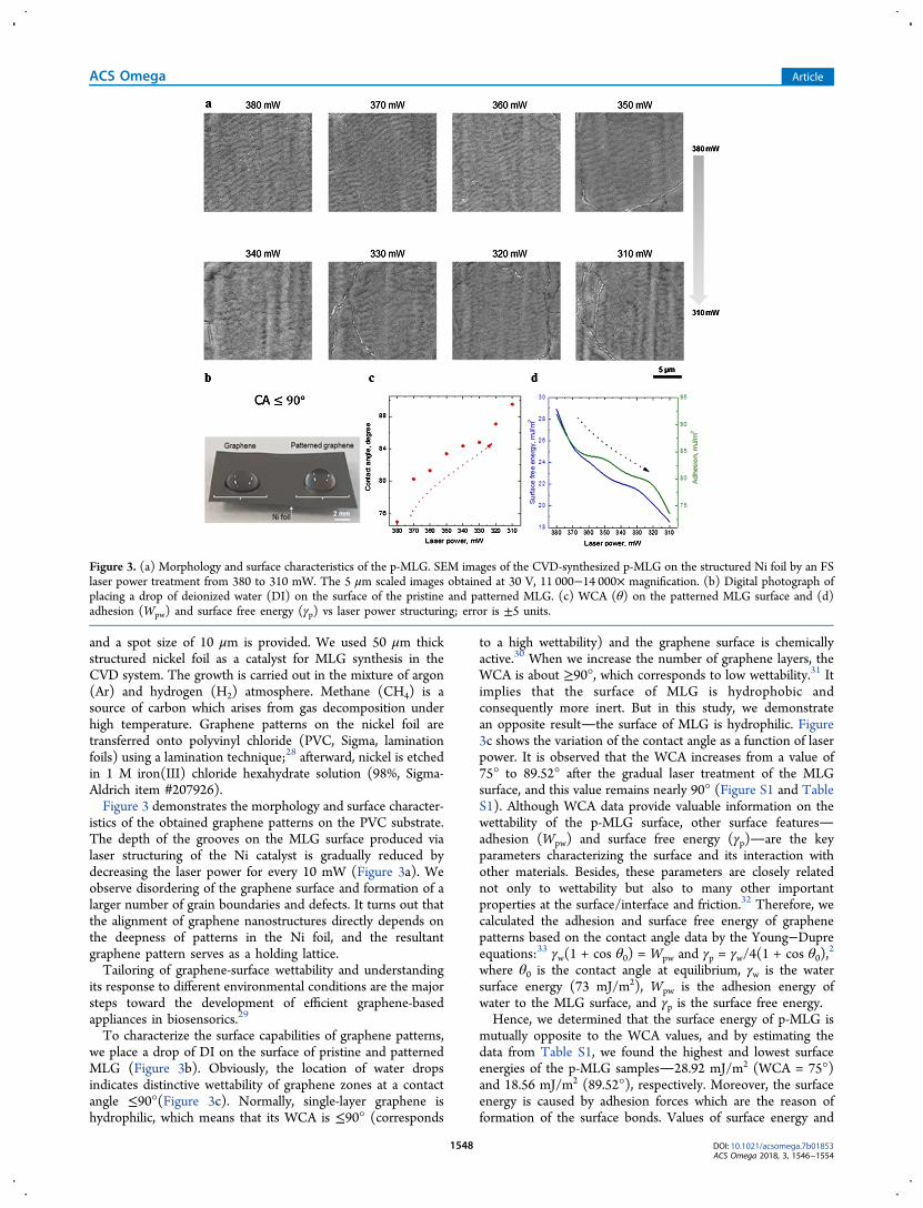
and a spot size of 10 μm is provided. We used 50 μm thickstructured nickel foil as a catalyst for MLG synthesis in theCVD system. The growth is carried out in the mixture of argon(Ar) and hydrogen (H2) atmosphere. Methane (CH4) is asource of carbon which arises from gas decomposition underhigh temperature. Graphene patterns on the nickel foil aretransferred onto polyvinyl chloride (PVC, Sigma, laminationfoils) using a lamination technique;28 afterward, nickel is etchedin 1 M iron(III) chloride hexahydrate solution (98%, Sigma-Aldrich item #207926).Figure 3 demonstrates the morphology and surface character-
istics of the obtained graphene patterns on the PVC substrate.The depth of the grooves on the MLG surface produced vialaser structuring of the Ni catalyst is gradually reduced bydecreasing the laser power for every 10 mW (Figure 3a). Weobserve disordering of the graphene surface and formation of alarger number of grain boundaries and defects. It turns out thatthe alignment of graphene nanostructures directly depends onthe deepness of patterns in the Ni foil, and the resultantgraphene pattern serves as a holding lattice.Tailoring of graphene-surface wettability and understanding
its response to different environmental conditions are the majorsteps toward the development of efficient graphene-basedappliances in biosensorics.29
To characterize the surface capabilities of graphene patterns,we place a drop of DI on the surface of pristine and patternedMLG (Figure 3b). Obviously, the location of water dropsindicates distinctive wettability of graphene zones at a contactangle ≤90°(Figure 3c). Normally, single-layer graphene ishydrophilic, which means that its WCA is ≤90° (corresponds
to a high wettability) and the graphene surface is chemicallyactive.30 When we increase the number of graphene layers, theWCA is about ≥90°, which corresponds to low wettability.31 Itimplies that the surface of MLG is hydrophobic andconsequently more inert. But in this study, we demonstratean opposite resultthe surface of MLG is hydrophilic. Figure3c shows the variation of the contact angle as a function of laserpower. It is observed that the WCA increases from a value of75° to 89.52° after the gradual laser treatment of the MLGsurface, and this value remains nearly 90° (Figure S1 and TableS1). Although WCA data provide valuable information on thewettability of the p-MLG surface, other surface featuresadhesion (Wpw) and surface free energy (γp)are the keyparameters characterizing the surface and its interaction withother materials. Besides, these parameters are closely relatednot only to wettability but also to many other importantproperties at the surface/interface and friction.32 Therefore, wecalculated the adhesion and surface free energy of graphenepatterns based on the contact angle data by the Young−Dupreequations:33 γw(1 + cos θ0) = Wpw and γp = γw/4(1 + cos θ0),
2
where θ0 is the contact angle at equilibrium, γw is the watersurface energy (73 mJ/m2), Wpw is the adhesion energy ofwater to the MLG surface, and γp is the surface free energy.Hence, we determined that the surface energy of p-MLG is
mutually opposite to the WCA values, and by estimating thedata from Table S1, we found the highest and lowest surfaceenergies of the p-MLG samples28.92 mJ/m2 (WCA = 75°)and 18.56 mJ/m2 (89.52°), respectively. Moreover, the surfaceenergy is caused by adhesion forces which are the reason offormation of the surface bonds. Values of surface energy and
Figure 3. (a) Morphology and surface characteristics of the p-MLG. SEM images of the CVD-synthesized p-MLG on the structured Ni foil by an FSlaser power treatment from 380 to 310 mW. The 5 μm scaled images obtained at 30 V, 11 000−14 000× magnification. (b) Digital photograph ofplacing a drop of deionized water (DI) on the surface of the pristine and patterned MLG. (c) WCA (θ) on the patterned MLG surface and (d)adhesion (Wpw) and surface free energy (γp) vs laser power structuring; error is ±5 units.
ACS Omega Article
DOI: 10.1021/acsomega.7b01853ACS Omega 2018, 3, 1546−1554
1548

adhesion are always linearly proportional (Figures 3d, S2, andS3); therefore, a higher surface energy corresponds to a higheradhesion and vice versa. Our results indicate lower surface freeenergy of all patterned graphene samples compared to thesurface free energy of water, which means that water partiallywets out the graphene surface. The graphene roughness formedby laser power treatment from 380 to 310 mW determines theincrease of the WCA and the surface free energy reduction, inother words, a degradation of the wettability and adhesion. Thesurface of the graphene produced with 310 mW laser power incomparison with the rest of the samples is more hydrophobic.To characterize the graphene patterns grown on various
structured Ni foils, Raman spectroscopic analysis is performedusing a laser excitation of 532 nm (Figure 4a). For singleRaman measurements, 20× objective and 20 s integration timeare used. The collected Raman spectra are the typical profiles offew-layer graphere/MLG. The main G- and 2D-peaks ofgraphene are clearly observed at around 1578 cm−1 (similar forall samples) and 2695−2706 cm−1, respectively. The fixedposition of G-peaks (Figure 4b) indicates stability in the planarvibrational mode of the sp2-hybridized carbon arrangement andconsequently determines the resemblance of graphene naturefor all obtained patterns. The negligible 2D band shapedifferences and its blue shift with decreasing laser power duringsurface structuring are caused by the decrease of the thickness/number of graphene layers34 (Figure 4b). Analyses of the peak
intensity ratio of the 2D- and G-bands are performed (Table S2and Figure S4). The I2D/G ratio of these bands for all graphenepatterns is equal to or less than “1”, which indicates few/multilayeredness. The appearance of a low-intensity D-band ineach case corresponds to the defect formation. Defectivenessstimulated by a laser beam via its contact with the Ni surface ismanifested as a fingerprint of the already imperfect structure.Nevertheless, the relatively stable I2D/G ratio in terms of laserpower and sharp symmetric 2D-bands is the confirmation for ahigh-quality patterned few-layer graphene/MLG.Because the groove depth of the p-MLG gradually decreases,
the graphene surface roughness increases, and the surfacebecomes hydrophobic under laser treatment, the electricaltransport property of graphene can be tuned by the surfacemorphology of the created patterns. Thus, the sheet resistance(Figure 4c) and optical transmittance (Figure 4d) of the p-MLG transferred on a PVC substrate are measured, and thisdemonstrated that patterning reduces the sheet resistance from16 to 10 Ω/sq despite the fact that the obtained p-MLG alreadypossesses low sheet resistance (about 20 Ω/sq). Besides, weidentified a directly proportional correlation between laserpower and the sheet resistance of grown graphene patterns:each reduction in the laser power of pattern processing reducesthe sheet resistance of the obtained p-MLG (e.g., 380 mWcorresponds to 16 Ω/sq and 310 mW corresponds to 10 Ω/sq).
Figure 4. Optical and electrical properties of the p-MLG. (a) General view of Raman spectra (G-, D-, and 2D-peaks) of MLG with different patterns.(b) Variation of Raman frequency as a function of laser power. (c) Variation of the sheet resistance of p-MLG as a function of laser power. The insetshows the schematic representation of the four-point measurement system. (d) Optical transmittance of the p-MLG on the PVC substrate vs laserpower.
ACS Omega Article
DOI: 10.1021/acsomega.7b01853ACS Omega 2018, 3, 1546−1554
1549
A variation of optical transmittance of the p-MLG on thePVC substrate at around 800 nm as a function of laser power isshown in Figures 4d, S5, and S6. We observed about 1.5 timesenhancement of optical transmittance with an increase of laserpower from 310 to 380 mW. It is known that when the numberof layers increases, the thickness becomes more uniform andresults in a decrease of optical transmittance.35 Apparently, thesheet thickness of the wrinkle configuration changesdecreasing32 with applied lower laser power. It means thatthinner and severe wrinklelike ordering of graphene withdeeper structuring (380 mW obtained p-MLG) providesenhanced optical transmittance.On the basis of the detailed morphological and electro-
optical investigation of p-MLG samples, structures fabricatedunder 380 mW are selected. Such a graphene pattern possessesa distinct structure alignment, acting as a holding lattice whichprevents defect appearance. It provides low sheet resistance (16Ω/sq) and higher optical transmittance in comparison withother graphene patterns. Additionally, the thickest 380 mWobtained p-MLG is more hydrophilic compared to otherproposed variety of patterns. The hydrophilicity providesreactivity to graphene patterns and impacts its surface area,which will significantly affect the performance of graphene-based devices. Therefore, we employed 380 mW obtained p-MLG for supercapacitor and Li-ion battery designs andcompared their performance with respect to the flatgraphene-based devices.We demonstrate the optical features of a graphene-enabled
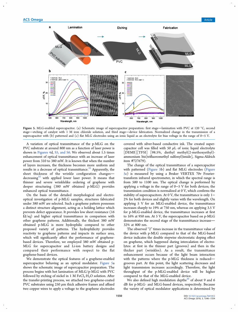
supercapacitor behaving as an optical modulator. Figure 5ashows the schematic image of supercapacitor preparation. Theprocess begins with hot lamination of MLG/p-MLG with PVCfollowed by etching of nickel in 1 M FeCl3·H2O solution. Afterthe transfer-printing process, we attached two graphene-coatedPVC substrates using 250 μm thick adhesive frames and affixedtwo copper wires to apply a voltage to the graphene electrodes
covered with silver-based conductive ink. The created super-capacitor cell was filled with 50 μL of ionic liquid electrolyte[DEME][TFSI] [98.5%, diethyl methyl(2-methoxyethyl)-ammonium bis(trifluoromethyl sulfonyl)imide], Sigma-Aldrichitem #727679).The change of the optical transmittance of a supercapacitor
with patterned (Figure 5b) and flat MLG electrodes (Figure5c) is measured by using a Bruker VERTEX 70v Fourier-transform infrared spectrometer, in which the spectral range isfrom 500 to 1100 nm. The optical change is performed byapplying a voltage in the range of 0−5 V for both devices; thetransmission condition is normalized at 0 V, which confirms thestability of supercapacitors. At 0 V, the transmittance is only 1−2% for both devices and slightly varies with the wavelength. Onapplying 5 V for an MLG-enabled device, the transmittanceincreases sharply to 19% at 750 nm, whereas on applying 3.5 Vfor p-MLG-enabled device, the transmittance increases at firstto 16% at 950 nm. At 5 V, the supercapacitor based on p-MLGdemonstrates the second stage of the transmittance increase32% at 800 nm.The observed “2” times increase in the transmittance value of
the device with p-MLG compared to that of the MLG-baseddevice indicates the double stepwise electrostatic doping effecton graphene, which happened during intercalation of electro-lytes: at first in the thinner part (grooves) and then in thethicker part (wrinkles). As a result, the transmittanceenhancement occurs because of the light beam interactionwith the patterns where the p-MLG thickness is reducedgrooves part. At this point, the light scattering decreases andlight transmission increases accordingly. Therefore, the lightthroughput of the p-MLG-enabled device will be highercompared to that of the MLG-enabled device.We also defined high modulation depths36 of about 9 and 6
dB for p-MLG- and MLG-based devices, respectively. Becausethe variety of optical modulator applications is determined by
Figure 5. MLG-enabled supercapacitor. (a) Schematic image of supercapacitor preparation: first stagelamination with PVC at 120 °C, secondstageetching of catalyst with 1 M iron chloride solution, and third stagedevice fabrication. Normalized change in the transmission of asupercapacitor with (b) patterned and (c) flat MLG electrodes using an ionic liquid as an electrolyte for bias voltage in the range of 0−5 V.
ACS Omega Article
DOI: 10.1021/acsomega.7b01853ACS Omega 2018, 3, 1546−1554
1550

the high modulation depth (>7 dB, as high-rate interconnectsand high-sensitivity sensing) and is limited when themodulation depth is less than ∼4 dB (as passive mode-lockingand short-distance data transmission),37 it is crucial to acquirethe modulation depth increase. Our results indicate broaderapplicability for p-MLG-enabled devices and their capability tooperate in the visible range as far as we are able to increase themodulation depth index by 1.5 times.Figure 6 represents a graphene-enabled battery structured as
a typical Li-ion battery. This device posturizes a single-cellbattery, where the electrodes are sandwiched symmetrically(Figure 6a,b). As an anode, we placed MLG/p-MLG on thepolymer substrate, which acted as an electrochromic layer aswell. To make good contact, we set a copper frame attached tothe graphene electrode. Lithium nickel manganese cobalt oxide(known in battery manufacturing as an NMC, Litarion) isoperated as a charge counter electrodecathodeproviding areversible electrochemical reaction. Finally, the electrodes areseparated using a 20 μm thick porous polyethylene membrane(PE, 42% porosity, Targray) soaked with 1 M lithiumhexafluorophosphate solution in ethylene carbonate and ethylmethyl carbonate (Sigma-Aldrich item #746738).We measured the capacitance of the MLG-enabled Li-ion
battery approximately 250 times, demonstrating negligibledecrease of its value with each next charging/dischargingcycle (Figure 6c). Inherently, all batteries gradually dischargeeventually whether they are used or not. This capacity loss istypically caused by slow parasitic reactions occurring within thebattery. The life cycle is the key for the good performance of abattery, and thus, increasing the life cycle is one of the firstparameters that should be focused on when aiming at providingefficiency of Li-ion batteries. Usually, heteroatom doping,
chemical impregnating, and hybridization of graphene electro-des are the best approaches to improve the prolongation of Li-ion batteries. For example, a graphene hybrid-based battery canyield 400 discharge/charge cycles with 0.01% capacity loss percycle.38 A battery in which the graphene electrode isimpregnated with sulfur demonstrates ultralong viability(2000 cycles and 0.028% capacity decay per cycle).39 In ourcase, the proposed battery with pure MLG demonstratedoperation for 1000 cycles (Figure 6d), which together with theassessed capacity (0.01% capacity loss per cycle) demonstratespromising results.On the other hand, the internal charge/discharge efficiency
plays a key role as well because slow discharging and fastcharging designed in a way to reduce the impact of self-heatingis required. To analyze the battery performance, the voltagedependence of charging/discharging processes by applyingconstant current (3 mA) for both devices is provided (Figure6e). We observed productivity reduction in the p-MLG-basedbattery when compared to the MLG-based battery because of adecrease of the charge/discharge time by approximately “2”times. This allows us to predetermine the viability of the p-MLG-enabled Li-ion battery during 500 cycles. The reductionin the number of life cycles is due to the change in the graphenesurface area after the patterning procedure. In fact, the patternsare artificially ordered defects that make graphene structuremore loosened and promote faster intercalation/deintercalationof Li-ions. Therefore, the presented approach could lead to newbifunctional applications combining the properties of energystorage and electrically switchable devices.
Figure 6. Graphene-enabled Li-ion battery. (a) Schematic image of the symmetrically constructed secondary battery based on the flat and (b)patterned MLG. MLG/p-MLG acted as an electrochromic layer (anode). Lithium nickel manganese cobalt oxide operated as a charge counterelectrode (cathode), providing a reversible electrochemical reaction in devices operating in the transmissive/reflective modes. (c) Galvanostaticdischarge/charge curves of the MLG-based battery after 1st, 2nd, 25th, 50th, and 250th measurements and (d) its life cycle as a function of time. (e)Voltage profiles for the constant current charge and discharge of Li-ion batteries incorporating MLG (green curve) and p-MLG (red curve) asnegative electrodes. The optical change results from an electric current of ≈3 mA at low dc potentials.
ACS Omega Article
DOI: 10.1021/acsomega.7b01853ACS Omega 2018, 3, 1546−1554
1551
■ CONCLUSIONS
In conclusion, we demonstrate a novel NLL technique for thepatterning of MLG via Ni catalyst substrate prestructuring.NLL provides contamination-free pattern replications intovarying geometrical shapes and sizes with a possibility totransfer p-MLG on the diverse substrates. The regulation ofhydrophobic/hydrophilic properties of graphene by variouslaser power adjustments is shown. The control of hydrophobic/hydrophilic properties defines the multifunctionality ofgraphene-enabled devices due to the graphene surface (dis)-ordering and, consequently, the formation of reactive oxygen-based functional groups. The distinct graphene structurealignment (which prevents defect appearance) assisted by thestrongest laser power (380 mW) contributes to certain p-MLGelectro-optical changes (sheet resistance decrease and opticaltransmittance enhancement). The p-MLG ability to operate asan electrically reconfigurable medium for supercapacitor and Li-ion battery designs are represented. The p-MLG-basedsupercapacitor testing results reveal 2 times transmittancevalue increase (in comparison with the MLG-based super-capacitor) caused by light interaction with patterned structureswhere its thickness is reduced. The p-MLG-based batteryindicates long-life viability (500 charging/discharging cycles)with 0.01% capacity loss per cycle; the negative feedbackleading toward twice the device productivity reduction whichoccurred due to graphene structure loosening after patterningand, consequently, (de)intercalation process accelerating. Weanticipate the NLL-based p-MLG to be a new approach toovercome the limitations imposed by the existing postsynthesisprocesses which will open a wide applicability gateway foradvanced graphene-based devices in energy storage, wearableelectronics, and biosensorics.
■ METHOD SUMMARY
Nonlinear Laser Lithography. The nanostructuring setupconsists of a FS laser system, GS, and motorized 3D-S (Figure1). The FS system is a home-made Yb-doped fiber laser (1030nm) which was reported before.40 It involves a dispersion-managed oscillator, a fiber stretcher, several amplification stagesand a grating compressor. The stretcher fiber was distributedbetween the amplifier stages to provide the optimal pulse peakpower during amplification to balance between the gain-narrowing and the self-phase modulation. The laser canproduce up to 1 μJ of pulse energy at a repetition rate of 1MHz, which corresponds to 1 W of average power. Theminimal pulse duration which can be obtained from the systemis 100 fs. Because the output light of the laser is linearlypolarized, the HWP placed between the laser and thepolarization beam splitter provides control of the laser poweron the sample. The second HWP allows the control ofpolarization on a sample. The sample was placed on themotorized 3D stage in the focal plane of the GS f-theta lens.The laser beam was scanned over the nickel surface in the
way that during every line scan it was partially overlapped withthe already created structure. In this way we preserved theconcept of nonlinear laser lithography,22 which allows coherentextension of the created structure over a large area surface, thus,improving the quality of the structure. The maximum scanningarea for our model of GS is 1 × 1 cm2. To extend the area, XYtranslation stage was used. With the given pulse energy andrepetition rate, the processing speed in our work was as fast as15 s for 1 × 1 cm2 area. It can be increased in the future by
scaling the repetition rate of the laser by keeping the pulseenergy constant, that is, simultaneously scaling the averagepower.
CVD Growth of Multilayer Graphene. A CVD systemwas used for the growth of MLG. The growth process wascarried out under ambient pressure in a 3″ quartz tube furnace,using 50 μm thick Ni foil. Argon gas was flushed into the quartztube for at least 5 min to remove oxygen. Afterward, hydrogenwas supplied while argon continued to run (ratio of Ar/H2 isabout 100/100 sccm). The gas-filled CVD system was left forheating till the temperature is raised to 1000 °C. Once 1000 °Ctemperature was reached, the methane flow is established at 30sccm together with the Ar/H2 flow at 100/100 sccm, followedby a waiting time of 5 min. In the end, the CH4 flow is turnedoff and the system is cooled down to room temperature in ∼1 hwhile keeping the Ar/H2 flow environment at 100/100 sccm.
Transfer Printing of Multilayer Graphene. Thefollowing steps are needed for the analysis of the MLG/p-MLG surface and fabrication of graphene-enabled devices afterCVD growth on a Ni foil. First, one side of the graphene-covered Ni foil was protected by paper, whereas the other sidewas in contact with PVC. Second, the patch of paper/graphene/Ni/graphene/PVC was sent through a laminationmachine with a temperature of about 120 °C. The obtainedPVC/graphene/Ni samples were then dipped in a 1 M FeCl2aqueous etching solution for a few hours. After the nickel wasetched, the PVC/graphene membranes were placed in DI for afew hours and rinsed as well. Then, the samples were blow-dried with N2 gas and were ready to use.
Characterization Methods.WCA of the MLG/p-MLG onPVC substrate was obtained using a home-made contact anglemeasurement setup. The setup consists of the followingelements: a white LED, XYZ translation stage with standardmicrometers (Thorlabs), video camera (Thorlabs, DCC1645C-USB 2.0 CMOS camera, 1280 × 1024, color sensor), and usualmedical syringe with a 200 μm diameter needle. We put a DIwater droplet of 4 μL on the investigated graphene surface andtook digital photographs. We measured the contact angles usinga program Screen Protractor which allows us to easily andquickly measure any angle on the screen to the nearest degree.The morphological analyses of the investigated graphenesamples were performed using scanning electron microscopy(Nova NanoSEM 600). To determine the graphitizationfingerprint and compare the defectiveness of MLG and p-MLG surfaces, a Jobin Yvon HORIBA Raman microscopesystem with 20× microscope objectives and 20 s integrationtime was used. The excitation wavelength was 532 nm. Thetransmittance measurements in the wavelength range between450 and 1100 nm were performed by using a Bruker VERTEX70v Fourier-transform infrared spectrometer integrated with aSi photodiode. The sheet resistance measurements were carriedout at four probe station platforms with the support of aKeithley 2600 multimeter. MLG was attached on the patternedarea to make Ohmic contact with the four electrodes. Then,sheet resistance was calculated using the standard formula (Rs =πR/ln 2 ≈ 4.53R).
Device Performance Characterization. Graphene-En-abled Supercapacitors. Optical measurements were performedin the 450−1100 nm wavelength range by a Bruker VERTEX70v Fourier-transform infrared spectrometer equipped with a Siphotodiode. Transmittance, Tp(λ), spectra were recorded bygraphene-based supercapacitors biased using the Keithley 2400Source measure unit.
ACS Omega Article
DOI: 10.1021/acsomega.7b01853ACS Omega 2018, 3, 1546−1554
1552
Graphene-Enabled Li-Ion Battery. The voltage and timereadings of charging/discharging processes were generatedusing the Keithley 2600 Source Meter instrument. The datawere collected under a constant current of 3 mA and processedwith LabVIEW software.
■ ASSOCIATED CONTENT
*S Supporting InformationThe Supporting Information is available free of charge on theACS Publications website at DOI: 10.1021/acsomega.7b01853.
Surface characteristics of patterned MLG; Ramancharacterization; and optical characterization (FiguresS5 and S6) (PDF)
■ AUTHOR INFORMATION
Corresponding Author*E-mail: [email protected] (E.K.).
ORCIDEvgeniya Kovalska: 0000-0002-8996-0790Anna Baldycheva: 0000-0002-2616-595XCoskun Kocabas: 0000-0003-0831-5552NotesThe authors declare no competing financial interest.
■ ACKNOWLEDGMENTS
This research was partially supported by the EuropeanResearch Council (ERC) Consolidator grants ERC-682723SmartGraphene and ERC-617521 NLL; the European Unionfunding: Marie Curie Fellowship visiting grant; and theEngineering and Physical Sciences Research Council(EPSRC) of the United Kingdom via grant no. EP/N035569/1. We thank our colleagues Dr. Nurbek Kakenov,Dr. Osman Balci, and Dr. Nassima Afshar Imani from BilkentUniversity who provided insight and expertise that greatlyassisted the research. We thank Dr. Omer Salihoglu(TUBITAK, Marmara Research Center) for the assistancewith capacity and life-cycle battery measurements, and MuratGure and Ergun Karaman (physicists and engineers of BilkentUniversity) for catalyst preparation and technical support. E.K.would also like to show her gratitude to all co-authors forsharing their pearls of wisdom and comments during thepreparation of manuscript that greatly improved its quality.
■ REFERENCES(1) Neto, A. H. C.; et al. The electronic properties of graphene. Rev.Mod. Phys. 2009, 81, 109.(2) Choi, W.; et al. Synthesis of graphene and its applications: Areview. Crit. Rev. Solid State Mater. Sci. 2010, 35, 52.(3) Shao, Y.; et al. Graphene based electrochemical sensors andbiosensors: A review. Electroanalysis 2010, 22, 1027.(4) Zhang, Y.; et al. Review of chemical vapor deposition of grapheneand related applications. Acc. Chem. Res. 2013, 46, 2329.(5) Han, M. Y.; et al. Energy band-gap engineering of graphenenanoribbons. Phys. Rev. Lett. 2007, 98, 206805.(6) Hicks, J.; et al. A wide-bandgap metal−semiconductor−metalnanostructure made entirely from graphene. Nat. Phys. 2013, 9, 49.(7) Jarvinen, P.; et al. Molecular self-assembly on graphene on SiO2and h-BN substrates. Nano Lett. 2013, 13, 3199.(8) Kang, S. J.; et al. Inking elastomeric stamps with micro-patterned,single layer graphene to create high-performance OFETs. Adv. Mater.2011, 23, 3531.
(9) Tapaszto, L.; et al. Tailoring the atomic structure of graphenenanoribbons by scanning tunnelling microscope lithography. Nat.Nanotechnol. 2008, 3, 397.(10) Zhang, L.; et al. Photocatalytic patterning and modification ofgraphene. J. Am. Chem. Soc. 2011, 133, 2706.(11) Jiao, L.; et al. Narrow graphene nanoribbons from carbonnanotubes. Nature 2009, 458, 877.(12) Kosynkin, D. V.; et al. Longitudinal unzipping of carbonnanotubes to form graphene nanoribbons. Nature 2009, 458, 872.(13) Zhang, W.; et al. Direct writing on graphene “paper” bymanipulating electrons as “invisible ink”. Nanotechnology 2013, 24,275301.(14) Feng, J.; et al. Patterning of graphene. Nanoscale 2012, 4, 4883.(15) Pang, S.; et al. Patterned graphene electrodes from solution-processed graphite oxide films for organic field-effect transistors. Adv.Mater. 2009, 21, 3488.(16) Kim, K. S.; et al. Large-scale pattern growth of graphene filmsfor stretchable transparent electrodes. Nature 2009, 457, 706.(17) Park, J. B.; et al. Fast growth of graphene patterns by laser directwriting. Appl. Phys. Lett. 2011, 98, 123109.(18) El-Kady, M. F.; et al. Laser scribing of high-performance andflexible graphene-based electrochemical capacitors. Science 2012, 335,1326.(19) Strong, V.; et al. Patterning and electronic tuning of laser scribedgraphene for flexible all-carbon devices. ACS Nano 2012, 6, 1395.(20) Chang, T.-L.; et al. Patterning of multilayer graphene on glasssubstrate by using ultraviolet picosecond laser pulses. Microelectron.Eng. 2016, 158, 1.(21) Kalita, G.; et al. Femtosecond laser induced micropatterning ofgraphene film. Mater. Lett. 2011, 65, 1569.(22) Oktem, B.; et al. Nonlinear laser lithography for indefinitelylarge-area nanostructuring with femtosecond pulses. Nat. Photonics2013, 7, 897.(23) Sipe, J. E.; et al. Laser-induced periodic surface structure I:theory. Phys. Rev. B: Condens. Matter Mater. Phys. 1983, 27, 1141.(24) Ardron, M.; et al. A practical technique for the generation ofhighly uniform LIPSS. Appl. Surf. Sci. 2014, 313, 123.(25) Bonse, J.; et al. Femtosecond laser-induced periodic surfacestructures. J. Laser Appl. 2012, 24, 042006.(26) Sun, Q.; et al. Nanograting formation on the surface of silicaglass by scanning focused femtosecond laser pulses. Opt. Lett. 2008,33, 2713.(27) Birnbaum, M. Semiconductor surface damage produced by rubylasers. J. Appl. Phys. 1965, 36, 3688.(28) Martins, L. G. P.; et al. Direct transfer of graphene onto flexiblesubstrates. Proc. Natl. Acad. Sci. U.S.A. 2013, 110, 17762.(29) Xu, K.; et al. Wetting: Contact with what? Nat. Mater. 2013, 12,872.(30) Li, Z.; et al. Effect of airborne contaminants on the wettability ofsupported graphene and graphite. Nat. Mater. 2013, 12, 925.(31) Raj, R.; et al. Wettability of Graphene. Nano Lett. 2013, 13,1509.(32) Chaudhury, M. K.; et al. Interfacial interaction between low-energy surfaces. Mater. Sci. Eng., R 1996, 16, 97.(33) Duca, M. D.; et al. Surface modifications of polyvinylidenefluoride (PVDF) under rf Ar plasma. Polym. Degrad. Stab. 1998, 61, 65.(34) Ferrari, A. C.; et al. Raman spectrum of graphene and graphenelayers. Phys. Rev. Lett. 2006, 97, 187401.(35) Zhu, S.-E.; et al. Optical transmittance of multilayer graphene.Europhys. Lett. 2014, 108, 17007.(36) Reed, G. T.; et al. Silicon optical modulators. Nat. Photonics2010, 4, 518.(37) Sun, Z.; et al. Optical modulators with 2D layered materials.Nat. Photonics 2016, 10, 227.(38) Sun, Y.; et al. Reconstruction of conformal nanoscale MnO ongraphene as a high-capacity and long-life anode material for lithium ionbatteries. Adv. Funct. Mater. 2013, 23, 2436.(39) Zhou, G.; et al. A graphene−pure-sulfur sandwich structure forultrafast, long-life lithium−sulfur batteries. Adv. Mater. 2014, 26, 625.
ACS Omega Article
DOI: 10.1021/acsomega.7b01853ACS Omega 2018, 3, 1546−1554
1553

(40) Pavlov, I.; et al. CLEO EUROPE/IQEC, 2013; p 1.
ACS Omega Article
DOI: 10.1021/acsomega.7b01853ACS Omega 2018, 3, 1546−1554
1554


![2 LASER INTERFERENCE LITHOGRAPHY - uni-halle.de · 2 LASER INTERFERENCE LITHOGRAPHY (LIL) 9 2 LASER INTERFERENCE LITHOGRAPHY (LIL) Laser interference lithography [3~22] (LIL) is a](https://static.fdocuments.in/doc/165x107/5eae180eecc7e273a41a4e88/2-laser-interference-lithography-uni-hallede-2-laser-interference-lithography.jpg)