NJIT ECE 271 Dr. Serhiy Levkov Topic 6 - 1 Topic 6 Analog Circuits Ideal Operational Amplifiers One...
184
NJIT ECE 271 Dr. Serhiy Levkov Topic 6 - 1 Topic 6 Analog Circuits Ideal Operational Amplifiers One Transistor Amplifier ECE 271 Electronic Circuits I
-
date post
19-Dec-2015 -
Category
Documents
-
view
232 -
download
7
Transcript of NJIT ECE 271 Dr. Serhiy Levkov Topic 6 - 1 Topic 6 Analog Circuits Ideal Operational Amplifiers One...

NJIT ECE 271 Dr. Serhiy Levkov Topic 6 - 1
Topic 6 Analog Circuits
Ideal Operational AmplifiersOne Transistor Amplifier
ECE 271
Electronic Circuits I

NJIT ECE 271 Dr. Serhiy Levkov
Example of Analog Electronic System: FM Stereo Receiver
• Linear functions: Radio and audio frequency amplification, frequency selection (tuning), impedance matching, local oscillator
• Nonlinear functions: DC power supply(rectification), frequency conversion (mixing), detection/demodulation
• The characteristics of signals are most often manipulated with linear amplifiers.
• Much information in the world (temperature, pressure, light intensity, sound, etc.) is analog in nature.
• In electric form those signals are transformed by different linear and nonlinear functions.
Topic 6 - 2

NJIT ECE 271 Dr. Serhiy Levkov
Amplification: Introduction
A complex periodic signal can be represented as the sum of many individual sine waves, one component of which has amplitude Vi = 1 mV and frequency ws with 0 phase (signal is used as reference):
After amplification, linear amplifier output is sinusoidal with same frequency but different amplitude VO and phase :
sini i s
v V t
(sin )o o s
v V t
Example: Audio amplifier. The input is a form of complicated periodic signal.
Topic 6 - 3
Ri
ii
vi
NJIT ECE 271 Dr. Serhiy Levkov
Amplification: Introduction (cont.)
Amplifier output power is:
If we need to deliver PO = 100 W and have RL = 8 , W then
This power results in output current:
where
Input current is given by (Vi = 1 mV )
and the phase is zero because circuit is purely resistive.
PO
Vo
2
21
RL
2 2 100 8 40Vo O L
V P R
(sin )o o si I t
Io V
oR
L
40V8 5A
-3810 V 1.82 10 A
5k 50ki
ii in
VI
R R
Topic 6 - 4

NJIT ECE 271 Dr. Serhiy Levkov
Amplification: Gain
The main parameter of an amplifier is the gain. Using phasor representation , we can introduce three types of gain.
• Voltage Gain (complex number):
Magnitude and phase of voltage gain are given by
and
For our example,
• Current Gain:
Magnitude of current gain is given by
0o o o
vi ii
V VA
VV
vv
ov
i
VA
V vA
43
40V 4 1010 V
ov
i
VA
V
0o o o
iii i
I IA
II
ii
8-8
5A 2.75 101.82 10 A
oi
i
IA
I
V v
Topic 6 - 5
NJIT ECE 271 Dr. Serhiy Levkov
Amplification: Gain (cont.)
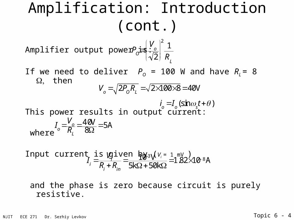
• Power Gain:
For our example,
The gain is often expressed in decibel scale:
2 2
2 2
o o
o oOv iP
i ii i i
V IP V IA A AP V I V I
AP 40 5
10 3 1.82 10 8 1.10 1013
AvdB
20logAv
AidB 20logA
i
APdB
10logAP
Topic 6 - 6

NJIT ECE 271 Dr. Serhiy Levkov
Two-port Model for Amplifier
• Simplifies amplifier-behavior modeling in complex systems.• Two-port (four terminal) models are linear network models, valid only
under small-signal conditions.• Represented by g-, h-, y- and z-parameters.• (v1, i1) and (v2, i2) represent signal components of voltages and
currents at the network ports.
Type of input-output model, black box that relates outputs to inputs.
input output
x1x2
Amplifier
Topic 6 - 7
NJIT ECE 271 Dr. Serhiy Levkov
Two-port Model Parameters• Theoretically, two-port model could be described fully by a 4x4 matrix or 16
parameters.• In practice, several sets of 4 parameters are used.
Topic 6 - 8

NJIT ECE 271 Dr. Serhiy Levkov
Two-port Model Parameters
Impedance (z)-parameters Admittance (y)-parameters
• Theoretically, two-port model could be described fully by a 4x4 matrix or 16 parameters.
• In practice, several sets of 4 parameters are used.
Topic 6 - 9

NJIT ECE 271 Dr. Serhiy Levkov
Two-port Model Parameters
Impedance (z)-parameters Admittance (y)-parameters
• Theoretically, two-port model could be described fully by a 4x4 matrix or 16 parameters.
• In practice, several sets of 4 parameters are used.
Hybrid (h)-parameters Inverse hybrid (g)-parameters
Topic 6 - 10

NJIT ECE 271 Dr. Serhiy Levkov
Two-port Model Parameters
Impedance (z)-parameters Admittance (y)-parameters
• Theoretically, two-port model could be described fully by a 4x4 matrix or 16 parameters.
• In practice, several sets of 4 parameters are used.
Hybrid (h)-parameters Inverse hybrid (g)-parameters
Transfer (A,B,C,D) -parameters
Topic 6 - 11
NJIT ECE 271 Dr. Serhiy Levkov
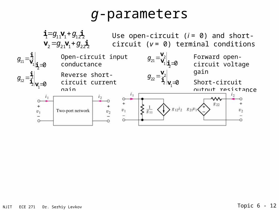
g-parameters
Use open-circuit (i = 0) and short-circuit (v = 0) terminal conditions2221212
2121111
ivvivi
gggg
111
12
112
21
0
0
g
g
iv
i
ii v
Open-circuit input conductance
Reverse short-circuit current gain
Forward open-circuit voltage gain
Short-circuit output resistance
221
12
222
21
0
0
g
g
vv i
vi v
Topic 6 - 12

NJIT ECE 271 Dr. Serhiy Levkov
g-parameters
Use open-circuit (i = 0) and short-circuit (v = 0) terminal conditions2221212
2121111
ivvivi
gggg
111
12
112
21
0
0
g
g
iv
i
ii v
Open-circuit input conductance
Reverse short-circuit current gain
Forward open-circuit voltage gain
Short-circuit output resistance
221
12
222
21
0
0
g
g
vv i
vi v
If g12 = 0Norton transformation
Topic 6 - 13

NJIT ECE 271 Dr. Serhiy Levkov
g-parameters: Example
Problem: Find g-parameters.Approach: Apply specified boundary conditions for each g-parameter, use circuit analysis.
For g11 and g21: apply voltage v1 to input port and open circuit output port. For g12 and g22: apply current i2 to output port and short circuit input port.
Topic 6 - 14

NJIT ECE 271 Dr. Serhiy Levkov
g-parameters: Example
Problem: Find g-parameters.Approach: Apply specified boundary conditions for each g-parameter, use circuit analysis.
For g11 and g21: apply voltage v1 to input port and open circuit output port. For g12 and g22: apply current i2 to output port and short circuit input port.
g11i
1v
1 i20
1210451(200k)
g119.7910 8S
g21v
2v
1 i20
g11
(51)(200k)0.998
222
2 v 01
112
2 v 01
v 1 391i 1 51
200k 20ki 391 0.0196i 20k
g
g
8 21 1 2
22 1 2
i 9.79 10 v 1.96 10 i
v 0.998v 3.91 10 i
Topic 6 - 15

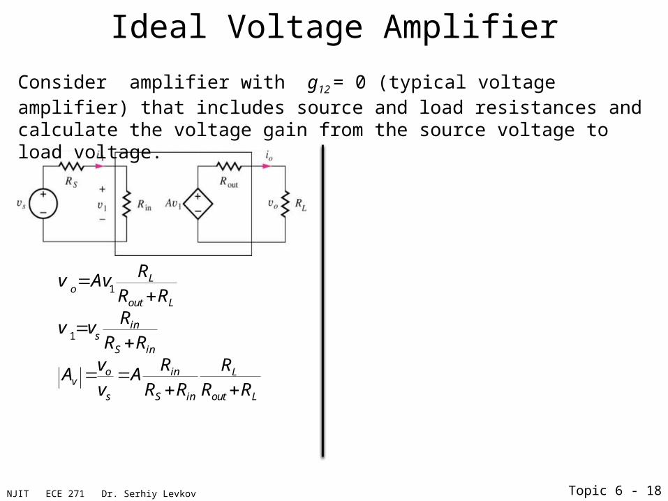
Ideal Voltage Amplifier
1
1
Lo
out L
ins
S in
o in Lv
s S in out L
Rv AvR RRv v
R RV R RA AV R R R R
Consider amplifier with g12 = 0 (typical voltage amplifier) that includes source and load resistances and calculate the voltage gain from the source voltage to load voltage.
NJIT ECE 271 Dr. Serhiy Levkov Topic 6 - 16

Ideal Voltage Amplifier
1
1
Lo
out L
ins
S in
o in Lv
s S in out L
Rv AvR RRv v
R RV R RA AV R R R R
Consider amplifier with g12 = 0 (typical voltage amplifier) that includes source and load resistances and calculate the voltage gain from the source voltage to load voltage.
NJIT ECE 271 Dr. Serhiy Levkov Topic 6 - 17
Ideal Voltage Amplifier
1
1
Lo
out L
ins
S in
o in Lv
s S in out L
Rv AvR RRv v
R Rv R RA Av R R R R
Consider amplifier with g12 = 0 (typical voltage amplifier) that includes source and load resistances and calculate the voltage gain from the source voltage to load voltage.
NJIT ECE 271 Dr. Serhiy Levkov Topic 6 - 18

Ideal Voltage Amplifier
1
1
Lo
out L
ins
S in
o in Lv
s S in out L
Rv AvR RRv v
R Rv R RA Av R R R R
Consider amplifier with g12 = 0 (typical voltage amplifier) that includes source and load resistances and calculate the voltage gain from the source voltage to load voltage.
NJIT ECE 271 Dr. Serhiy Levkov Topic 6 - 19
Conclusion: full gain depends on source and load parameters.

Ideal Voltage Amplifier
1
1
Lo
out L
ins
S in
o in Lv
s S in out L
Rv AvR RRv v
R Rv R RA Av R R R R
Consider amplifier with g12 = 0 (typical voltage amplifier) that includes source and load resistances and calculate the voltage gain from the source voltage to load voltage.
NJIT ECE 271 Dr. Serhiy Levkov Topic 6 - 20
Conclusion: full gain depends on source and load parameters.
How to make it non- dependent?

Ideal Voltage Amplifier
1
1
Lo
out L
ins
S in
o in Lv
s S in out L
Rv AvR RRv v
R RV R RA AV R R R R
Rin >> Rs and Rout<< RL,
Av A
Ideal voltage amplifier: Rout = 0,
Rin
Consider amplifier with g12 = 0 (typical voltage amplifier) that includes source and load resistances and calculate the voltage gain from the source voltage to load voltage.
NJIT ECE 271 Dr. Serhiy Levkov Topic 6 - 21
Conclusion: full gain depends on source and load parameters.
How to make it non- dependent?

Ideal Voltage Amplifier
1
1
Lo
out L
ins
S in
o in Lv
s S in out L
Rv AvR RRv v
R RV R RA AV R R R R
Rin >> Rs and Rout<< RL,
Av A
Ideal voltage amplifier: Rout = 0,
Rin
1
o
o L o S in S ini v
s s L L
S in
VV R R R RI RA AV R RVI
R R
Consider amplifier with g12 = 0 (typical voltage amplifier) that includes source and load resistances and calculate the voltage gain from the source voltage to load voltage.
NJIT ECE 271 Dr. Serhiy Levkov Topic 6 - 22
Conclusion: full gain depends on source and load parameters.
For current:
How to make it non- dependent?

Other Amplifier Types
NJIT ECE 271 Dr. Serhiy Levkov Topic 6 - 23
Voltage amplifier
0,i o
R R 0
(V/V)ovo
i io
vA v
Current amplifier
0
(A/A)ois
i vo
iA i
0,
i oR R
Transconductance amplifier
0
(A/V)om
i vo
iG v
,i o
R R
Transresistance amplifier
0
(V/A)om
i io
vR i
00,i o
R R

Other Amplifier Types
NJIT ECE 271 Dr. Serhiy Levkov Topic 6 - 24
Voltage amplifier
0,i o
R R 0
(V/V)ovo
i io
vA v
Current amplifier
0
(A/A)ois
i vo
iA i
0,
i oR R
Transconductance amplifier
0
(A/V)om
i vo
iG v
,i o
R R
Transresistance amplifier
0
(V/A)om
i io
vR i
00,i o
R R

Other Amplifier Types
NJIT ECE 271 Dr. Serhiy Levkov Topic 6 - 25
Voltage amplifier
0,i o
R R 0
(V/V)ovo
i io
vA v
Current amplifier
0
(A/A)ois
i vo
iA i
0,
i oR R
Transconductance amplifier
0
(A/V)om
i vo
iG v
,i o
R R
Transresistance amplifier
0
(V/A)om
i io
vR i
00,i o
R R

Other Amplifier Types
NJIT ECE 271 Dr. Serhiy Levkov Topic 6 - 26
Voltage amplifier
0,i o
R R 0
(V/V)ovo
i io
vA v
Current amplifier
0
(A/A)ois
i vo
iA i
0,
i oR R
Transconductance amplifier
0
(A/V)om
i vo
iG v
,i o
R R
Transresistance amplifier
0
(V/A)om
i io
vR i
00,i o
R R

Other Amplifier Types
NJIT ECE 271 Dr. Serhiy Levkov Topic 6 - 27
Voltage amplifier
0,i o
R R 0
(V/V)ovo
i io
vA v
Current amplifier
0
(A/A)ois
i vo
iA i
0,
i oR R
Transconductance amplifier
0
(A/V)om
i vo
iG v
,i o
R R
Transresistance amplifier
0
(V/A)om
i io
vR i
00,i o
R R

Operational Amplifier (Op Amp)
NJIT ECE 271 Dr. Serhiy Levkov
• Op amp is a fundamental building block in electronic design. They are cheap mass produced IC and can be used to build many different types of electronic devices like instrumentation amplifiers, active filters, rectifiers, A/D and D/A converters, and others.
• Typical integrated circuit amplifier: LM386N (~ $1.00 each)• The practical op amp is a form of differential amplifier: responds to a difference
of two input signals. Typically: VCC >0, VEE <0 – so the voltages are symmetric 5V, 10V, 18V.
Topic 6 - 28

NJIT ECE 271 Dr. Serhiy Levkov
Differential Amplifier – Signal Amplification
A - open-circuit voltage gain,
A =10, Adb =20log(10) = 20 db
vID = (v+-v--) - differential input signal
vID = VID + vid = 1 + 0.25sin t, where
VID – dc value, vid – signal component
vO = VO + vo = 5 + 2.5sin t
The typical voltage transfer characteristic for a differential amplifier biased by two symmetric power supplies:
Topic 6 - 29

NJIT ECE 271 Dr. Serhiy Levkov
Distortion in Amplifiers• If the ac input signal exceeds 0.5V, the output signal will be clipped off (see vO2 ) and
get distorted. • Different gains for positive and negative values of input also cause distortion in output.• Total Harmonic Distortion (THD) is a measure of signal distortion that compares
undesired harmonic content of a signal to the desired component.
v(t) VO V
1(sin
ot
1) V
2(sin2
ot
2) V
3(sin3
ot
3) ...
dcdesired output
2nd harmonic distortion
3rd harmonic distortion
THD100% V
i
2
i 2
V1
Topic 6 - 30
NJIT ECE 271 Dr. Serhiy Levkov
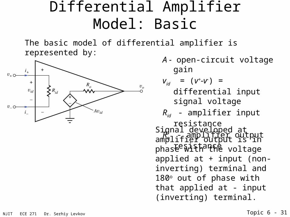
Differential Amplifier Model: Basic
A - open-circuit voltage gain
vid = (v+-v-) = differential input signal voltage
Rid - amplifier input resistance
Ro - amplifier output resistance
Signal developed at amplifier output is in phase with the voltage applied at + input (non-inverting) terminal and 180o out of phase with that applied at - input (inverting) terminal.
The basic model of differential amplifier is represented by:
Topic 6 - 31

NJIT ECE 271 Dr. Serhiy Levkov
Differential Amplifier Model: With Source and Load
RL = load resistanceRS = Thevenin equivalent resistance of
signal sourcevs = Thevenin equivalent voltage of
signal sourceL
o L
RA
o id R R
v v
Topic 6 - 32

NJIT ECE 271 Dr. Serhiy Levkov
Differential Amplifier Model: With Source and Load
RL = load resistanceRS = Thevenin equivalent resistance of
signal sourcevs = Thevenin equivalent voltage of
signal sourceL
o L
RA
o id R R
v v
Rid
id s R Rid s
v vand
Topic 6 - 33

NJIT ECE 271 Dr. Serhiy Levkov
Differential Amplifier Model: With Source and Load
RL = load resistanceRS = Thevenin equivalent resistance of
signal sourcevs = Thevenin equivalent voltage of
signal sourceL
o L
RA
o id R R
v v
Rid
id s R Rid s
v vand
Topic 6 - 34
vo
vs
R Rid LA A
v R R R Rid S o L

NJIT ECE 271 Dr. Serhiy Levkov
Differential Amplifier Model: With Source and Load (Example)
• Problem: Calculate voltage gain• Given Data: A=100, Rid =100kW, Ro = 100W, RS =10kW, RL =1000W
o
s
100k 100038.3dB
10k 100k 100 1000100 82.6
R Rid LA A
v R R R Rid S o L
v
v
Topic 6 - 35

NJIT ECE 271 Dr. Serhiy Levkov
Differential Amplifier Model: With Source and Load (Example)
• Problem: Calculate voltage gain• Given Data: A=100, Rid =100kW, Ro = 100W, RS =10kW, RL =1000W
• Ideal amplifier’s output depends only on input voltage difference and not on source and load resistances. This can be achieved by using resistance condition (Rid >> RS or infinite Rid and Ro << RL or zero Ro ):
A - open-loop gain (maximum voltage gain available from the device)
o
s
100k 100038.3dB
10k 100k 100 1000100 82.6
R Rid LA A
v R R R Rid S o L
v
v
o
idA A
v
v
v
Topic 6 - 36

NJIT ECE 271 Dr. Serhiy Levkov
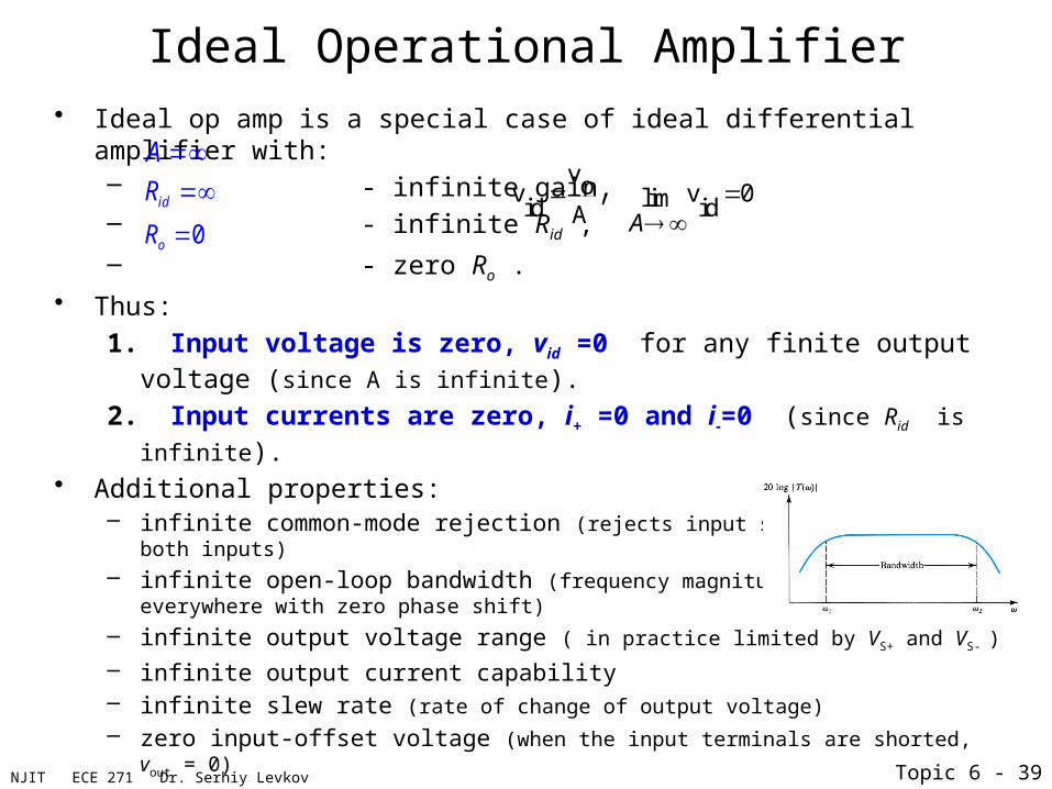
Ideal Operational Amplifier• Ideal op amp is a special case of ideal differential amplifier with:
– - infinite gain, – - infinite Rid ,
– - zero Ro .
Topic 6 - 37
A
idR
0oR
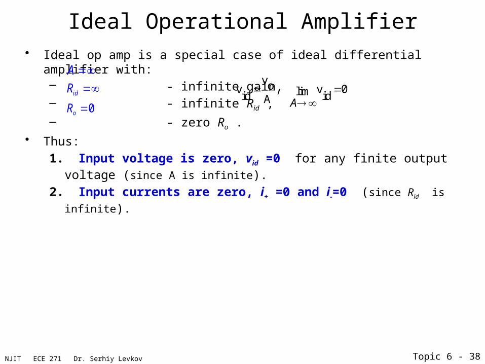
NJIT ECE 271 Dr. Serhiy Levkov
Ideal Operational Amplifier• Ideal op amp is a special case of ideal differential amplifier with:
– - infinite gain, – - infinite Rid ,
– - zero Ro .
• Thus:
1. Input voltage is zero, vid =0 for any finite output voltage (since A is infinite).
2. Input currents are zero, i+ =0 and i-=0 (since Rid is infinite).
,vov v 0limid idA A
Topic 6 - 38
A
idR
0oR
NJIT ECE 271 Dr. Serhiy Levkov
Ideal Operational Amplifier• Ideal op amp is a special case of ideal differential amplifier with:
– - infinite gain, – - infinite Rid ,
– - zero Ro .
• Thus:
1. Input voltage is zero, vid =0 for any finite output voltage (since A is infinite).
2. Input currents are zero, i+ =0 and i-=0 (since Rid is infinite).
• Additional properties:– infinite common-mode rejection (rejects input signals common to both inputs)
– infinite open-loop bandwidth (frequency magnitude response is flat everywhere with zero phase shift)
– infinite output voltage range ( in practice limited by VS+ and VS- )
– infinite output current capability – infinite slew rate (rate of change of output voltage)
– zero input-offset voltage (when the input terminals are shorted, vout = 0)
• The major benefit of ideal op-amp: the same standard op-amp allows to build various circuits with very specific properties by using external to op-amp circuit elements. The classic op-amps circuits are considered further.
,vov v 0limid idA A
Topic 6 - 39
A
idR
0oR

NJIT ECE 271 Dr. Serhiy Levkov
Inverting Amplifier: Configuration
• Non-inverting input is grounded.• Feedback network (resistor R2 ) is connected between
inverting input and output• Input network (resistor R1 ) is connected between
inverting input and signal source.
Topic 6 - 40

NJIT ECE 271 Dr. Serhiy Levkov
Inverting Amplifier:Voltage Gain
1 2 2KVL: - 0
S Oi iv R Rs v
Topic 6 - 41

NJIT ECE 271 Dr. Serhiy Levkov
Inverting Amplifier:Voltage Gain
1 2 2KVL: - 0
S Oi iv R Rs v
Topic 6 - 42
22KCL: 0ii i i ss i

NJIT ECE 271 Dr. Serhiy Levkov
Inverting Amplifier:Voltage Gain
1 2 2KVL: - 0
S Oi iv R Rs v
Topic 6 - 43
22KCL: 0ii i i ss i since 0 by 2i

NJIT ECE 271 Dr. Serhiy Levkov
Inverting Amplifier:Voltage Gain
1 2 2KVL: - 0
S Oi iv R Rs v
Topic 6 - 44
22KCL: 0ii i i ss i since 0 by 2i
1 1S
v vsiR
vsR

NJIT ECE 271 Dr. Serhiy Levkov
Inverting Amplifier:Voltage Gain
1 2 2KVL: - 0
S Oi iv R Rs v
Topic 6 - 45
22KCL: 0ii i i ss i since 0 by 2i
1 1S
v vsiR
vsR
since 0 and 0 by 1
idv v

NJIT ECE 271 Dr. Serhiy Levkov
Inverting Amplifier:Voltage Gain
1 2 2KVL: - 0
S Oi iv R Rs v
Topic 6 - 46
22KCL: 0ii i i ss i since 0 by 2i
1 1S
v vsiR
vsR
since 0 and 0 by 1
idv v
Substituting iS and i2 into KVL:
2
1
2
1
orS O
vv RoA
v v Rs
RvR
1 2 1 1 2 1
1
( ) 0 ( ) 0SS O S S O
v R R v R R R v RR
v v v

NJIT ECE 271 Dr. Serhiy Levkov
Inverting Amplifier:Voltage Gain
1 2 2KVL: - 0
S Oi iv R Rs v
Topic 6 - 47
22KCL: 0ii i i ss i since 0 by 2i
1 1S
v vsiR
vsR
since 0 and 0 by 1
idv v
Substituting iS and i2 into KVL:
2
1
2
1
orS O
vv RoA
v v Rs
RvR
Conclusions:• The gain of the inverting op-amp circuit is determined by R1 and R2 .
• The gain is a result of imposing the negative feedback.• Gain is greater than 1 if R2 > R1. Gain is less than 1 if R1 > R2
• Negative voltage gain implies 1800 phase shift between input and output signals.• Inverting input of op amp is at ground potential (not connected directly to ground) and is
said to be at virtual ground.
1 2 1 1 2 11
( ) 0 ( ) 0SS O S S O
v R R v R R R v RR
v v v

NJIT ECE 271 Dr. Serhiy Levkov
Inverting Amplifier: Input and Output Resistances
1nin i
vsRis
R R
Topic 6 - 48
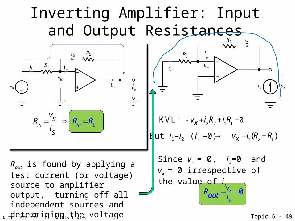
NJIT ECE 271 Dr. Serhiy Levkov
Inverting Amplifier: Input and Output Resistances
1nin i
vsRis
R R 2 2 1 10KVL: v i R i Rx
But i1=i2 (i- =0) 1 2 1( )v i R Rx
Since v- = 0, i1=0 and vx = 0 irrespective of the value of ix ,
0x
x
vi
Rout
Topic 6 - 49
Rout is found by applying a test current (or voltage) source to amplifier output, turning off all independent sources and determining the voltage (or current):

NJIT ECE 271 Dr. Serhiy Levkov
Inverting Amplifier: Example
• Problem: Design an inverting amplifier with
Av=40 dB, Rin =20kW,
• Assumptions: Ideal op amp
Topic 6 - 50
• Convert the gain from db:
• Input resistance is controlled by R1 and voltage gain is set by R2 / R1.
Thus
and
40/20[db] 20log 40 10 100v
A A Av v
120k
inR R
22 1
1
100 2RA R R Mv R

NJIT ECE 271 Dr. Serhiy Levkov
Summing Amplifier
• Scale factors for the 2 inputs can be independently adjusted by proper choice of R2 and R1.
• Any number of inputs can be connected to summing junction through extra resistors.
• This is an example of a simple digital-to-analog converter.
11
1
vi
R 2
22
vi
R 3
3
Ov
iR
Since negative amplifier input is at virtual ground (vid = 0):
Since i-=0, i3= i1 + i2,
3 31 2
1 2
R Rv v vo R R
Topic 6 - 51
vid

NJIT ECE 271 Dr. Serhiy Levkov
Non-inverting Amplifier: Configuration
• Input signal is applied to the non-inverting input terminal.• Portion of the output signal is fed back to the negative input terminal.• Analysis is done by relating voltage at v1 to input voltage vs and output
voltage vo .
Topic 6 - 52

NJIT ECE 271 Dr. Serhiy Levkov
Non-inverting Amplifier: Analysis
Since i-=0, (voltage divider) 11
1 2
Rv vo R R
Topic 6 - 53
+- vid
i-
i+

NJIT ECE 271 Dr. Serhiy Levkov
Non-inverting Amplifier: Analysis
Since i-=0,
From KVL
11
1 2
Rv vo R R
10
S idv v v
Topic 6 - 54
+- vid
i-
i+

NJIT ECE 271 Dr. Serhiy Levkov
Non-inverting Amplifier: Analysis
Since i-=0,
From KVL , since vid =0
and
11
1 2
Rv vo R R
10
S idv v v
1v vs
1 2
1
R Rv vo s R
Topic 6 - 55
+- vid
i-
i+

NJIT ECE 271 Dr. Serhiy Levkov
Non-inverting Amplifier: Analysis
Since i-=0,
From KVL , since vid =0
and
.
11
1 2
Rv vo R R
10
S idv v v
1v vs
1 2
1
R Rv vo s R
Topic 6 - 56
21 2
1 1
1v R R RoA
v Rv Rs
+- vid
i-
i+

NJIT ECE 271 Dr. Serhiy Levkov
Non-inverting Amplifier: Analysis
Since i-=0,
From KVL , since vid =0
and
.
11
1 2
Rv vo R R
10
S idv v v
1v vs
1 2
1
R Rv vo s R
Topic 6 - 57
21 2
1 1
1v R R RoA
v Rv Rs
+- vid
i-
i+
Since i+=0, . in
vsRi

NJIT ECE 271 Dr. Serhiy Levkov
Non-inverting Amplifier: Analysis
Since i-=0,
From KVL , since vid =0
and
.
11
1 2
Rv vo R R
10
S idv v v
1v vs
1 2
1
R Rv vo s R
Since i+=0, .
Rout is found by applying a test current source to amplifier output and setting vs = 0 and is identical to the output resistance of inverting amplifier i.e. Rout =0.
Topic 6 - 58
21 2
1 1
1v R R RoA
v Rv Rs
+- vid
i-
i+
in
vsRi
21 2
1 1
1v R R RoA
v Rv Rs

NJIT ECE 271 Dr. Serhiy Levkov
Non-inverting Amplifier: Analysis
Since i-=0,
From KVL , since vid =0
and
.
11
1 2
Rv vo R R
10
S idv v v
1v vs
1 2
1
R Rv vo s R
Since i+=0, .
Rout is found by applying a test current source to amplifier output and setting vs = 0 and is identical to the output resistance of inverting amplifier i.e. Rout =0.
Topic 6 - 59
21 2
1 1
1v R R RoA
v Rv Rs
+- vid
i-
i+
in
vsRi
21 2
1 1
1v R R RoA
v Rv Rs
2
1
,1 RAv R , 0
in outR R

NJIT ECE 271 Dr. Serhiy Levkov
Non-inverting Amplifier: Example
• Problem: Determine the characteristics of given non-inverting amplifier.
• Given Data: R1= 3kW, R2 =43kW, vs=+0.1 V
• Assumptions: Ideal op amp.• Analysis:
Since i-=0,
2
1
15.343k1 13k
(15.3)(0.1 ) 1.53V
RAv R
v A v Vo sv
2 1
1.53 33.343 3
OO
v Vi AR R k k
Topic 6 - 60
+- vid
i-
i+
io

NJIT ECE 271 Dr. Serhiy Levkov
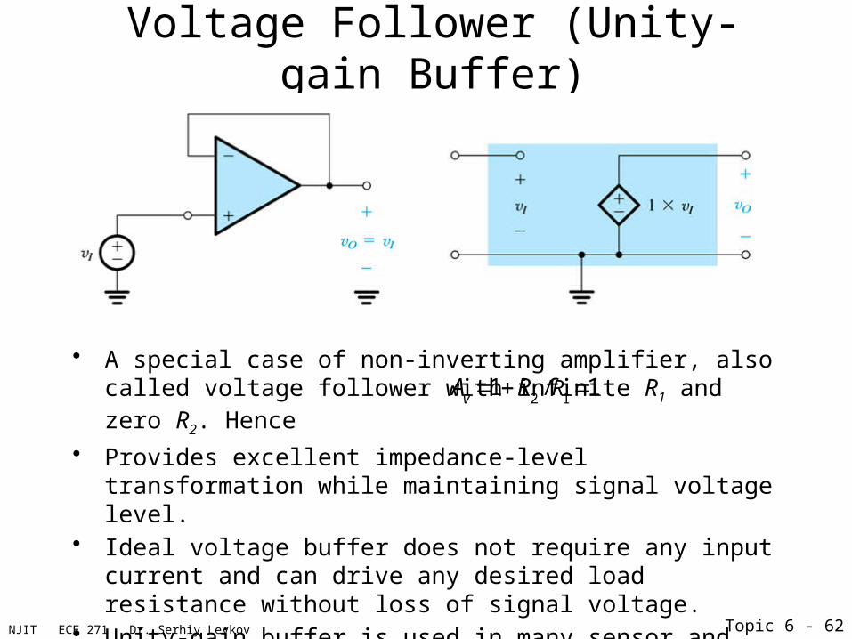
Voltage Follower (Unity-gain Buffer)
Topic 6 - 61
NJIT ECE 271 Dr. Serhiy Levkov
Voltage Follower (Unity-gain Buffer)
• A special case of non-inverting amplifier, also called voltage follower with infinite R1 and zero R2. Hence
• Provides excellent impedance-level transformation while maintaining signal voltage level.
• Ideal voltage buffer does not require any input current and can drive any desired load resistance without loss of signal voltage.
• Unity-gain buffer is used in many sensor and data acquisition systems.
Topic 6 - 62
2 1/1 1
vRA R

NJIT ECE 271 Dr. Serhiy Levkov
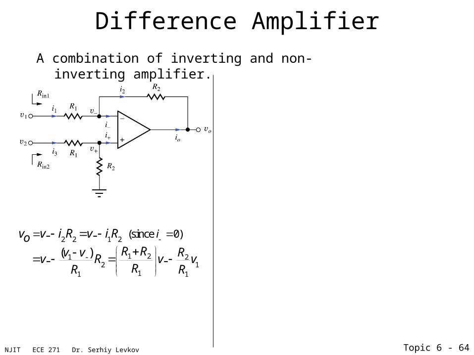
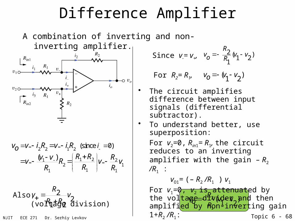
Difference Amplifier
Topic 6 - 63
A combination of inverting and non-inverting amplifier.
NJIT ECE 271 Dr. Serhiy Levkov
Difference Amplifier
Topic 6 - 64
A combination of inverting and non-inverting amplifier.
2 2 1 2
1 21 - 22 1
11 1
(since 0)- -
( )- -
iv v i R v i RoR Rv v Rv R v v
RR R

NJIT ECE 271 Dr. Serhiy Levkov
Difference Amplifier
2 2 1 2
1 21 - 22 1
11 1
(since 0)- -
( )- -
iv v i R v i RoR Rv v Rv R v v
RR R
Also, (voltage division)
Topic 6 - 65
A combination of inverting and non-inverting amplifier.
22
1 2
Rv v
R R

NJIT ECE 271 Dr. Serhiy Levkov
Difference Amplifier
Since v-= v+, 2 ( )1 21
Rv v vo R
For R2= R1, ( )1 2
v v vo
Topic 6 - 66
A combination of inverting and non-inverting amplifier.
2 2 1 2
1 21 - 22 1
11 1
(since 0)- -
( )- -
iv v i R v i RoR Rv v Rv R v v
RR R
22
1 2
Rv v
R R
Also, (voltage division)

NJIT ECE 271 Dr. Serhiy Levkov
Difference Amplifier
• The circuit amplifies difference between input signals (differential subtractor).
Since v-= v+, 2 ( )1 21
Rv v vo R
For R2= R1, ( )1 2
v v vo
Topic 6 - 67
A combination of inverting and non-inverting amplifier.
2 2 1 2
1 21 - 22 1
11 1
(since 0)- -
( )- -
iv v i R v i RoR Rv v Rv R v v
RR R
22
1 2
Rv v
R R
Also, (voltage division)
NJIT ECE 271 Dr. Serhiy Levkov
Difference Amplifier
• The circuit amplifies difference between input signals (differential subtractor).
• To understand better, use superposition:
For v2=0, Rin1= R1, the circuit reduces to an inverting amplifier with the gain – R2 /R1 :
vO1= (– R2 /R1 ) v1
For v1=0, v2 is attenuated by the voltage divider and then amplified by non-inverting gain 1+R2 /R1:
vO2= (R2 /(R1 +R1 ))(1+ R2 /R1 ) v2
Then vO = vO1 + vO2,
Since v-= v+, 2 ( )1 21
Rv v vo R
For R2= R1, ( )1 2
v v vo
Topic 6 - 68
A combination of inverting and non-inverting amplifier.
2
1
v (v v )1 2
Ro R
2 2 1 2
1 21 - 22 1
11 1
(since 0)- -
( )- -
iv v i R v i RoR Rv v Rv R v v
RR R
22
1 2
Rv v
R R
Also, (voltage division)

NJIT ECE 271 Dr. Serhiy Levkov
Difference Amplifier: Example
Topic 6 - 69
Do example on the board

NJIT ECE 271 Dr. Serhiy Levkov
Difference Amplifier: Example
• Problem: Determine Vo, V+, V-, Io, I1, I2, I3 .
• Given Data: R1= 10kW, R2 =100kW, V1= 5V, V2=3V
• Assumptions: Ideal op amp.
Hence, V-= V+ and I-= I+= 0.
• Analysis:
1002 3 2.732- 10 1001 2
R kV V V V VR R k k
5 -2.731 - 227
1 2 101
V V V VI I AR k
5 (227 )(110 ) 20.01 1 1 2 2
V V I R I R V A k Vo
2272
I I Ao
Topic 6 - 70
0 32 273 1101 2
V VI AR R k

NJIT ECE 271 Dr. Serhiy Levkov
Integrator
Topic 6 - 71

NJIT ECE 271 Dr. Serhiy Levkov
Integrator
• Feedback resistor R2 in the inverting amplifier is replaced by capacitor C.
• The circuit uses frequency-dependent feedback.
Rsv
si dt
odvCci
Topic 6 - 72

NJIT ECE 271 Dr. Serhiy Levkov
Integrator
• Feedback resistor R2 in the inverting amplifier is replaced by capacitor C.
• The circuit uses frequency-dependent feedback.
Rsv
si dt
odvCci
Topic 6 - 73
Since ic= is ,1
sv
RC
dvodt

NJIT ECE 271 Dr. Serhiy Levkov
Integrator
• Feedback resistor R2 in the inverting amplifier is replaced by capacitor C.
• The circuit uses frequency-dependent feedback.
Rsv
si dt
odvCci
Since ic= is ,
1( ) ( ) (0)0
(0) (0)
1
tv t v d vo s
dv v dso RC
oRC
v Vo c
Topic 6 - 74
1s
vRC
dvodt
Voltage at the circuit’s output at time t is given by the initial capacitor voltage plus integral of the input signal from start of
integration interval, here, t=0.

NJIT ECE 271 Dr. Serhiy Levkov
Integrator
• Feedback resistor R2 in the inverting amplifier is replaced by capacitor C.
• The circuit uses frequency-dependent feedback.
Rsv
si dt
odvCci
Since ic= is ,
1( ) ( ) (0)0
(0) (0)
1
tv t v d vo s
dv v dso RC
oRC
v Vo c
Topic 6 - 75
1s
vRC
dvodt
Voltage at the circuit’s output at time t is given by the initial capacitor voltage plus integral of the input signal from start of
integration interval, here, t=0.
Voltage at the circuit’s output at time t is given by the initial capacitor voltage plus integral of the input signal from start of
integration interval, here, t=0.
Integration of an input step signal results in a ramp at the output.

NJIT ECE 271 Dr. Serhiy Levkov
Differentiator
Topic 6 - 76

NJIT ECE 271 Dr. Serhiy Levkov
Differentiator
Topic 6 - 77
• Input resistor R1 in the inverting amplifier is replaced by capacitor C.

NJIT ECE 271 Dr. Serhiy Levkov
Differentiator
• Input resistor R1 in the inverting amplifier is replaced by capacitor C.
Rov
Ri dt
sdvCsi
Since iR= is
dtsdv
RCov
Topic 6 - 78

NJIT ECE 271 Dr. Serhiy Levkov
Differentiator
• Input resistor R1 in the inverting amplifier is replaced by capacitor C.
Rov
Ri dt
sdvCsi
Since iR= is
dtsdv
RCov
Output is scaled version of derivative of input voltage.
Topic 6 - 79

NJIT ECE 271 Dr. Serhiy Levkov
Differentiator
• Input resistor R1 in the inverting amplifier is replaced by capacitor C.
Rov
Ri dt
sdvCsi
Since iR= is
dtsdv
RCov
Topic 6 - 80
Derivative operation emphasizes high-frequency components of input signal, hence is less often used than the integrator.
Output is scaled version of derivative of input voltage.

NJIT ECE 271 Dr. Serhiy Levkov
Op-Amps – What’s Next
• Frequency dependent feedback (cont. ch 10):– high, low and band pass amplifiers (filters)– integrators and differentiators
Topic 6 - 81

NJIT ECE 271 Dr. Serhiy Levkov
Op-Amps – What’s Next
• Frequency dependent feedback (cont. ch 10):– high, low and band pass amplifiers (filters)– integrators and differentiators
• Analysis of non-ideal amplifiers (ch. 11)• Amplifier frequency response and stability (ch. 11)
Topic 6 - 82

NJIT ECE 271 Dr. Serhiy Levkov
Op-Amps – What’s Next
• Frequency dependent feedback (cont. ch 10):– high, low and band pass amplifiers (filters)– integrators and differentiators
• Analysis of non-ideal amplifiers (ch. 11)• Amplifier frequency response and stability (ch. 11)• Op-amps applications (ch. 12)
– instrumentation amplifiers – active filters– D/A and A/D converters– Oscillators– Nonlinear circuits (precision rectifiers)– Circuits with positive feedback (comparators, triggers)
Topic 6 - 83

NJIT ECE 271 Dr. Serhiy Levkov
Op-Amps – What’s Next
• Frequency dependent feedback (cont. ch 10):– high, low and band pass amplifiers (filters)– integrators and differentiators
• Analysis of non-ideal amplifiers (ch. 11)• Amplifier frequency response and stability (ch. 11)• Op-amps applications (ch. 12)
– instrumentation amplifiers – active filters– D/A and A/D converters– Oscillators– Nonlinear circuits (precision rectifiers)– Circuits with positive feedback (comparators, triggers)
• Single transistor amplifiers – linear amplification and small signal model (ch. 13)
Topic 6 - 84

NJIT ECE 271 Dr. Serhiy Levkov
Op-Amps – What’s Next
• Frequency dependent feedback (cont. ch 10):– high, low and band pass amplifiers (filters)– integrators and differentiators
• Analysis of non-ideal amplifiers (ch. 11)• Amplifier frequency response and stability (ch. 11)• Op-amps applications (ch. 12)
– instrumentation amplifiers – active filters– D/A and A/D converters– Oscillators– Nonlinear circuits (precision rectifiers)– Circuits with positive feedback (comparators, triggers)
• Single transistor amplifiers – linear amplification and small signal model (ch. 13)• Single transistor amplifiers – detailed design (ch. 14)
Topic 6 - 85

NJIT ECE 271 Dr. Serhiy Levkov
Op-Amps – What’s Next
• Frequency dependent feedback (cont. ch 10):– high, low and band pass amplifiers (filters)– integrators and differentiators
• Analysis of non-ideal amplifiers (ch. 11)• Amplifier frequency response and stability (ch. 11)• Op-amps applications (ch. 12)
– instrumentation amplifiers – active filters– D/A and A/D converters– Oscillators– Nonlinear circuits (precision rectifiers)– Circuits with positive feedback (comparators, triggers)
• Single transistor amplifiers – linear amplification and small signal model (ch. 13)• Single transistor amplifiers – detailed design (ch. 14)• Op-amps design (multistage amplifiers) (ch. 15)
What do we study in this course?
Topic 6 - 86

NJIT ECE 271 Dr. Serhiy Levkov
Op-Amps – What’s Next
• Frequency dependent feedback (cont. ch 10):– high, low and band pass amplifiers (filters)– integrators and differentiators
• Analysis of non-ideal amplifiers (ch. 11)• Amplifier frequency response and stability (ch. 11)• Op-amps applications (ch. 12)
– instrumentation amplifiers – active filters– D/A and A/D converters– Oscillators– Nonlinear circuits (precision rectifiers)– Circuits with positive feedback (comparators, triggers)
• Single transistor amplifiers – linear amplification and small signal model (ch. 13)• Single transistor amplifiers – detailed design (ch. 14)• Op-amps design (multistage amplifiers) (ch. 15)
Topic 6 - 87

NJIT ECE 271 Dr. Serhiy Levkov Topic 6 - 88NJIT ECE 271 Dr. Serhiy Levkov
Transistors as Amplifiers

NJIT ECE 271 Dr. Serhiy Levkov Topic 6 - 89NJIT ECE 271 Dr. Serhiy Levkov
Transistors as AmplifiersIn this section we will study • The general techniques for employing individual transistors as amplifiers

NJIT ECE 271 Dr. Serhiy Levkov Topic 6 - 90NJIT ECE 271 Dr. Serhiy Levkov
Transistors as AmplifiersIn this section we will study • The general techniques for employing individual transistors as amplifiers • Operation of common source MOSFET amplifier
NJIT ECE 271 Dr. Serhiy Levkov Topic 6 - 91NJIT ECE 271 Dr. Serhiy Levkov
Transistors as AmplifiersIn this section we will study • The general techniques for employing individual transistors as amplifiers • Operation of common source MOSFET amplifier• Operation of common emitter BJT amplifier

NJIT ECE 271 Dr. Serhiy Levkov Topic 6 - 92NJIT ECE 271 Dr. Serhiy Levkov
Transistors as Amplifiers
What do we know:• MOSFET (FET) can be used as amplifier if operated in saturation region (SR)
In this section we will study • The general techniques for employing individual transistors as amplifiers • Operation of common source MOSFET amplifier• Operation of common emitter BJT amplifier
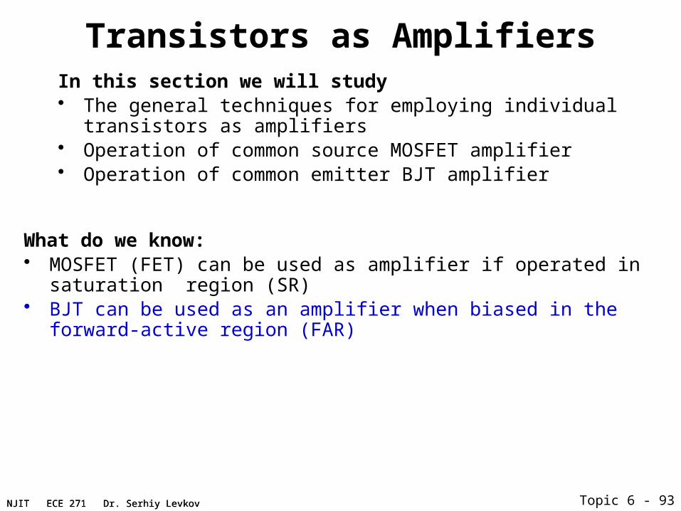
NJIT ECE 271 Dr. Serhiy Levkov Topic 6 - 93NJIT ECE 271 Dr. Serhiy Levkov
Transistors as Amplifiers
What do we know:• MOSFET (FET) can be used as amplifier if operated in saturation region (SR) • BJT can be used as an amplifier when biased in the forward-active region (FAR)
In this section we will study • The general techniques for employing individual transistors as amplifiers • Operation of common source MOSFET amplifier• Operation of common emitter BJT amplifier

NJIT ECE 271 Dr. Serhiy Levkov Topic 6 - 94NJIT ECE 271 Dr. Serhiy Levkov
Transistors as Amplifiers
What do we know:• MOSFET (FET) can be used as amplifier if operated in saturation region (SR) • BJT can be used as an amplifier when biased in the forward-active region (FAR)• We will refer to the FAR and SR as to the “active region”
In this section we will study • The general techniques for employing individual transistors as amplifiers • Operation of common source MOSFET amplifier• Operation of common emitter BJT amplifier

NJIT ECE 271 Dr. Serhiy Levkov Topic 6 - 95NJIT ECE 271 Dr. Serhiy Levkov
Transistors as Amplifiers
What do we know:• MOSFET (FET) can be used as amplifier if operated in saturation region (SR) • BJT can be used as an amplifier when biased in the forward-active region (FAR)• We will refer to the FAR and SR as to the “active region” • In these regions, transistors can provide high voltage, current and power gains
In this section we will study • The general techniques for employing individual transistors as amplifiers • Operation of common source MOSFET amplifier• Operation of common emitter BJT amplifier

NJIT ECE 271 Dr. Serhiy Levkov Topic 6 - 96NJIT ECE 271 Dr. Serhiy Levkov
Transistors as Amplifiers
What do we know:• MOSFET (FET) can be used as amplifier if operated in saturation region (SR) • BJT can be used as an amplifier when biased in the forward-active region (FAR)• We will refer to the FAR and SR as to the “active region” • In these regions, transistors can provide high voltage, current and power gains• Bias is provided to stabilize the operating point in a desired operation region
In this section we will study • The general techniques for employing individual transistors as amplifiers • Operation of common source MOSFET amplifier• Operation of common emitter BJT amplifier

NJIT ECE 271 Dr. Serhiy Levkov Topic 6 - 97NJIT ECE 271 Dr. Serhiy Levkov
Transistors as Amplifiers
What do we know:• MOSFET (FET) can be used as amplifier if operated in saturation region (SR) • BJT can be used as an amplifier when biased in the forward-active region (FAR)• We will refer to the FAR and SR as to the “active region” • In these regions, transistors can provide high voltage, current and power gains• Bias is provided to stabilize the operating point in a desired operation region• The Q-point also determines
– Small-signal parameters of transistor– Voltage gain, input resistance, output resistance– Maximum input and output signal amplitudes– Power consumption
In this section we will study • The general techniques for employing individual transistors as amplifiers • Operation of common source MOSFET amplifier• Operation of common emitter BJT amplifier

NJIT ECE 271 Dr. Serhiy Levkov Topic 6 - 98NJIT ECE 271 Dr. Serhiy Levkov
BJT Amplifier
Consider a BJT , biased in active region by dc voltage source VBE = 0.7V.
1510 , 100, 0.025)(s F T
VI

NJIT ECE 271 Dr. Serhiy Levkov Topic 6 - 99NJIT ECE 271 Dr. Serhiy Levkov
BJT Amplifier
Consider a BJT , biased in active region by dc voltage source VBE = 0.7V.
From the simplified FAR model we get:
1510 , 100, 0.025)(s F T
VI
15μA 1.5mA 10 3.3 10 3.3 1.5 5
VBEVS T
B C F CE CBF
II e I I V K I V

NJIT ECE 271 Dr. Serhiy Levkov Topic 6 - 100NJIT ECE 271 Dr. Serhiy Levkov
BJT Amplifier
Consider a BJT , biased in active region by dc voltage source VBE = 0.7V.
From the simplified FAR model we get:
1510 , 100, 0.025)(s F T
VI
15μA 1.5mA 10 3.3 10 3.3 1.5 5
VBEVS T
B C F CE CBF
II e I I V K I V

NJIT ECE 271 Dr. Serhiy Levkov Topic 6 - 101NJIT ECE 271 Dr. Serhiy Levkov
BJT Amplifier
Consider a BJT , biased in active region by dc voltage source VBE = 0.7V.
From the simplified FAR model we get:
1510 , 100, 0.025)(s F T
VI
15μA 1.5mA 10 3.3 10 3.3 1.5 5
VBEVS T
B C F CE CBF
II e I I V K I V

NJIT ECE 271 Dr. Serhiy Levkov Topic 6 - 102NJIT ECE 271 Dr. Serhiy Levkov
BJT Amplifier
Consider a BJT , biased in active region by dc voltage source VBE = 0.7V.
From the simplified FAR model we get:
Thus the Q-point is set at (IC, VCE) = (1.5 mA, 5 V)
1510 , 100, 0.025)(s F T
VI
15μA 1.5mA 10 3.3 10 3.3 1.5 5
VBEVS T
B C F CE CBF
II e I I V K I V

NJIT ECE 271 Dr. Serhiy Levkov Topic 6 - 103NJIT ECE 271 Dr. Serhiy Levkov
BJT Amplifier
Now let’s inject the sin signal with the amplitude 8 mV by adding the voltage source vbe The total base-emitter voltage becomes:
vBEV
BEv
be

NJIT ECE 271 Dr. Serhiy Levkov Topic 6 - 104NJIT ECE 271 Dr. Serhiy Levkov
BJT Amplifier
Now let’s inject the sin signal with the amplitude 8 mV by adding the voltage source vbe The total base-emitter voltage becomes:
From the FAR model for VBEh = 0.708V and VBEl = 0.692V we will get
vBEV
BEv
be
μA and20 10μABh Bl
I I

NJIT ECE 271 Dr. Serhiy Levkov Topic 6 - 105NJIT ECE 271 Dr. Serhiy Levkov
BJT Amplifier
Now let’s inject the sin signal with the amplitude 8 mV by adding the voltage source vbe The total base-emitter voltage becomes:
From the FAR model for VBEh = 0.708V and VBEl = 0.692V we will get
vBEV
BEv
be
Thus 8 mV peak change in vBE : 5 mA change in iB and 0.5 mA change in iC.
20μA and 10μABh Bl
I I

NJIT ECE 271 Dr. Serhiy Levkov Topic 6 - 106NJIT ECE 271 Dr. Serhiy Levkov
BJT Amplifier
Now let’s inject the sin signal with the amplitude 8 mV by adding the voltage source vbe The total base-emitter voltage becomes:
From the FAR model for VBEh = 0.708V and VBEl = 0.692V we will get
vBEV
BEv
be
Thus 8 mV peak change in vBE : 5 mA change in iB and 0.5 mA change in iC.
From the load line equation this will produce the 1.65V change in vCE . 330010CE C
v i
20μA and 10μABh Bl
I I
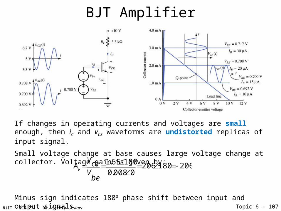
NJIT ECE 271 Dr. Serhiy Levkov Topic 6 - 107NJIT ECE 271 Dr. Serhiy Levkov
If changes in operating currents and voltages are small enough, then iC and vCE waveforms are undistorted replicas of input signal.
Small voltage change at base causes large voltage change at collector. Voltage gain is given by:
Minus sign indicates 1800 phase shift between input and output signals.
Av
VceV
be
1.65 1800.008 0
206 180 206
BJT Amplifier

NJIT ECE 271 Dr. Serhiy Levkov Topic 6 - 108NJIT ECE 271 Dr. Serhiy Levkov
MOSFET Amplifier
Consider MOSFET biased in active region by dc voltage source VGS = 3.5 V, which
Will set the Q-point at (ID, VDS) = (1.56 mA, 4.8 V).
Then we introduce the signal vGS and total gate-source voltage becomes
vGS V
GS v
gs
Doing similar analisis as for BJT, we get :
1 V change in vGS 1.25 mA change in iD 4 V change in vDS.

NJIT ECE 271 Dr. Serhiy Levkov Topic 6 - 109NJIT ECE 271 Dr. Serhiy Levkov
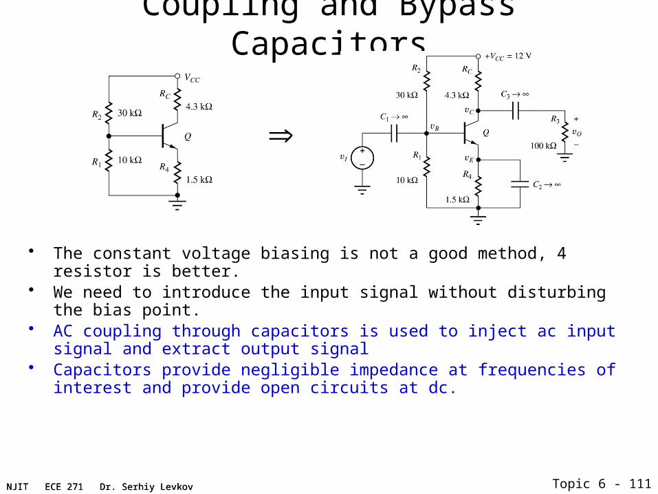
Coupling and Bypass Capacitors
• The constant voltage biasing is not a good method, 4 resistor is better.

NJIT ECE 271 Dr. Serhiy Levkov Topic 6 - 110NJIT ECE 271 Dr. Serhiy Levkov
Coupling and Bypass Capacitors
• The constant voltage biasing is not a good method, 4 resistor is better.• We need to introduce the input signal without disturbing the bias point.
NJIT ECE 271 Dr. Serhiy Levkov Topic 6 - 111NJIT ECE 271 Dr. Serhiy Levkov
Coupling and Bypass Capacitors
• The constant voltage biasing is not a good method, 4 resistor is better.• We need to introduce the input signal without disturbing the bias point.• AC coupling through capacitors is used to inject ac input signal and extract output
signal• Capacitors provide negligible impedance at frequencies of interest and provide open
circuits at dc.
NJIT ECE 271 Dr. Serhiy Levkov Topic 6 - 112NJIT ECE 271 Dr. Serhiy Levkov
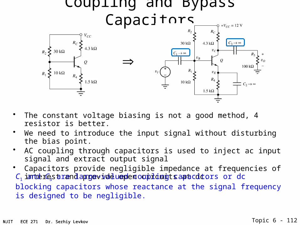
Coupling and Bypass Capacitors
• The constant voltage biasing is not a good method, 4 resistor is better.• We need to introduce the input signal without disturbing the bias point.• AC coupling through capacitors is used to inject ac input signal and extract output
signal• Capacitors provide negligible impedance at frequencies of interest and provide open
circuits at dc.
C1 and C3 are large-valued coupling capacitors or dc blocking capacitors whose reactance at the signal frequency is designed to be negligible.

NJIT ECE 271 Dr. Serhiy Levkov Topic 6 - 113NJIT ECE 271 Dr. Serhiy Levkov
Coupling and Bypass Capacitors
• The constant voltage biasing is not a good method, 4 resistor is better.• We need to introduce the input signal without disturbing the bias point.• AC coupling through capacitors is used to inject ac input signal and extract output
signal• Capacitors provide negligible impedance at frequencies of interest and provide open
circuits at dc.
C1 and C3 are large-valued coupling capacitors or dc blocking capacitors whose reactance at the signal frequency is designed to be negligible.
C2 is a bypass capacitor that provides a low impedance path for ac current from emitter to ground thereby removing RE from the circuit when ac signals are considered.

NJIT ECE 271 Dr. Serhiy Levkov Topic 6 - 114NJIT ECE 271 Dr. Serhiy Levkov
DC and AC Analysis
• DC analysis:– Make dc equivalent circuit by replacing all capacitors by open circuits
and inductors by short circuits.– Find Q-point from dc equivalent circuit by using appropriate large-
signal transistor model.

NJIT ECE 271 Dr. Serhiy Levkov Topic 6 - 115NJIT ECE 271 Dr. Serhiy Levkov
DC and AC Analysis
• DC analysis:– Make dc equivalent circuit by replacing all capacitors by open circuits
and inductors by short circuits.– Find Q-point from dc equivalent circuit by using appropriate large-
signal transistor model.
• AC analysis:– Make ac equivalent circuit by replacing all capacitors by short circuits,
inductors by open circuits, dc voltage sources by ground connections and dc current sources by open circuits.

NJIT ECE 271 Dr. Serhiy Levkov Topic 6 - 116NJIT ECE 271 Dr. Serhiy Levkov
DC and AC Analysis
• DC analysis:– Make dc equivalent circuit by replacing all capacitors by open circuits
and inductors by short circuits.– Find Q-point from dc equivalent circuit by using appropriate large-
signal transistor model.
• AC analysis:– Make ac equivalent circuit by replacing all capacitors by short circuits,
inductors by open circuits, dc voltage sources by ground connections and dc current sources by open circuits.
– Replace transistor by small-signal model
NJIT ECE 271 Dr. Serhiy Levkov Topic 6 - 117NJIT ECE 271 Dr. Serhiy Levkov
DC and AC Analysis
• DC analysis:– Make dc equivalent circuit by replacing all capacitors by open circuits
and inductors by short circuits.– Find Q-point from dc equivalent circuit by using appropriate large-
signal transistor model.
• AC analysis:– Make ac equivalent circuit by replacing all capacitors by short circuits,
inductors by open circuits, dc voltage sources by ground connections and dc current sources by open circuits.
– Replace transistor by small-signal model– Use small-signal ac equivalent to analyze ac characteristics of amplifier.

NJIT ECE 271 Dr. Serhiy Levkov Topic 6 - 118NJIT ECE 271 Dr. Serhiy Levkov
DC and AC Analysis
• DC analysis:– Make dc equivalent circuit by replacing all capacitors by open circuits
and inductors by short circuits.– Find Q-point from dc equivalent circuit by using appropriate large-
signal transistor model.
• AC analysis:– Make ac equivalent circuit by replacing all capacitors by short circuits,
inductors by open circuits, dc voltage sources by ground connections and dc current sources by open circuits.
– Replace transistor by small-signal model– Use small-signal ac equivalent to analyze ac characteristics of amplifier.– Combine end results of dc and ac analysis to yield total voltages and
currents in the network.

NJIT ECE 271 Dr. Serhiy Levkov Topic 6 - 119NJIT ECE 271 Dr. Serhiy Levkov
DC Equivalent for MOSFET Amplifier
dc equivalent
ac equivalent Simplified ac equivalent
Full circuit
Make dc equivalent circuit by replacing all

NJIT ECE 271 Dr. Serhiy Levkov Topic 6 - 120NJIT ECE 271 Dr. Serhiy Levkov
dc equivalent
ac equivalent Simplified ac equivalent
Full circuit
Make dc equivalent circuit by replacing all - capacitors by open circuits
DC Equivalent for MOSFET Amplifier
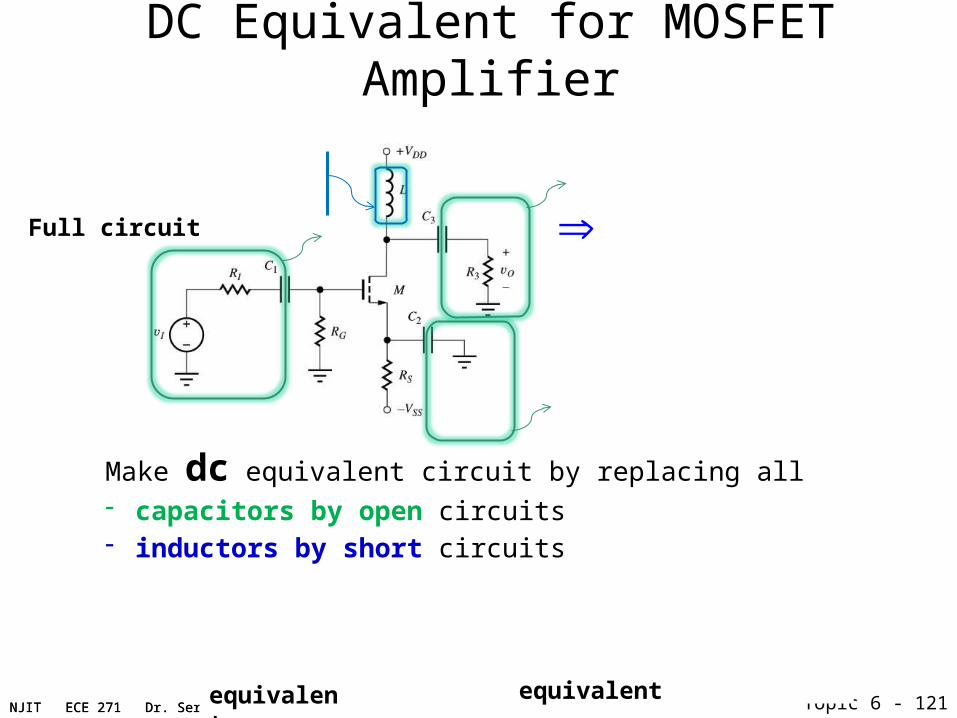
NJIT ECE 271 Dr. Serhiy Levkov Topic 6 - 121NJIT ECE 271 Dr. Serhiy Levkov
dc equivalent
ac equivalent Simplified ac equivalent
Full circuit
Make dc equivalent circuit by replacing all - capacitors by open circuits - inductors by short circuits
DC Equivalent for MOSFET Amplifier

NJIT ECE 271 Dr. Serhiy Levkov Topic 6 - 122NJIT ECE 271 Dr. Serhiy Levkov
dc equivalent
ac equivalent Simplified ac equivalent
Full circuit
Make dc equivalent circuit by replacing all - capacitors by open circuits - inductors by short circuits
DC Equivalent for MOSFET Amplifier

NJIT ECE 271 Dr. Serhiy Levkov Topic 6 - 123NJIT ECE 271 Dr. Serhiy Levkov
AC Equivalent for MOSFET Amplifier
dc equivalent
ac equivalent Simplified ac equivalent
Full circuit
Make ac equivalent circuit by replacing all - capacitors by short circuits

NJIT ECE 271 Dr. Serhiy Levkov Topic 6 - 124NJIT ECE 271 Dr. Serhiy Levkov
AC Equivalent for MOSFET Amplifier
dc equivalent
ac equivalent Simplified ac equivalent
Full circuit
Make ac equivalent circuit by replacing all - capacitors by short circuits - inductors by open circuits

NJIT ECE 271 Dr. Serhiy Levkov Topic 6 - 125NJIT ECE 271 Dr. Serhiy Levkov
AC Equivalent for MOSFET Amplifier
dc equivalent
ac equivalent Simplified ac equivalent
Full circuit
Make ac equivalent circuit by replacing all - capacitors by short circuits - inductors by open circuits - dc voltage sources by ground connections

NJIT ECE 271 Dr. Serhiy Levkov Topic 6 - 126NJIT ECE 271 Dr. Serhiy Levkov
AC Equivalent for MOSFET Amplifier
dc equivalent
ac equivalent Simplified ac equivalent
Full circuit
Make ac equivalent circuit by replacing all - capacitors by short circuits - inductors by open circuits - dc voltage sources by ground connections- dc current sources by open circuits
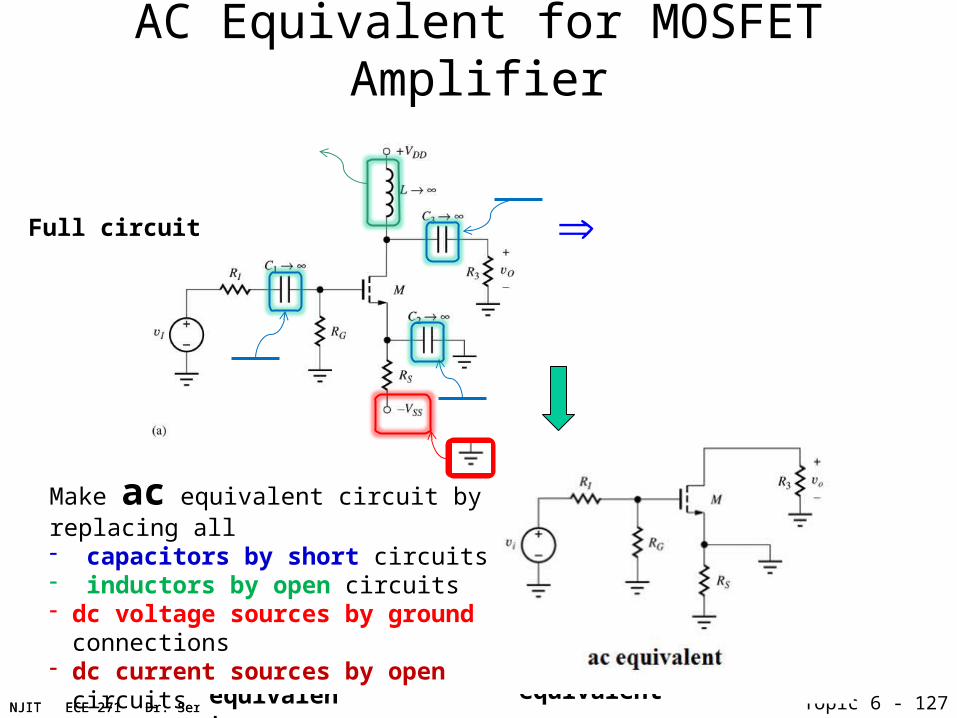
NJIT ECE 271 Dr. Serhiy Levkov Topic 6 - 127NJIT ECE 271 Dr. Serhiy Levkov
AC Equivalent for MOSFET Amplifier
dc equivalent
ac equivalent Simplified ac equivalent
Full circuit
Make ac equivalent circuit by replacing all - capacitors by short circuits - inductors by open circuits - dc voltage sources by ground connections- dc current sources by open circuits

NJIT ECE 271 Dr. Serhiy Levkov Topic 6 - 128NJIT ECE 271 Dr. Serhiy Levkov
dc equivalent
ac equivalent Simplified ac equivalent
Full circuit
AC Equivalent for MOSFET Amplifier
Simplify the ac equivalent circuit

NJIT ECE 271 Dr. Serhiy Levkov Topic 6 - 129NJIT ECE 271 Dr. Serhiy Levkov
DC and AC Equivalents for MOSFET Amplifier
dc equivalent
ac equivalent Simplified ac equivalent
Full circuit

NJIT ECE 271 Dr. Serhiy Levkov Topic 6 - 130NJIT ECE 271 Dr. Serhiy Levkov
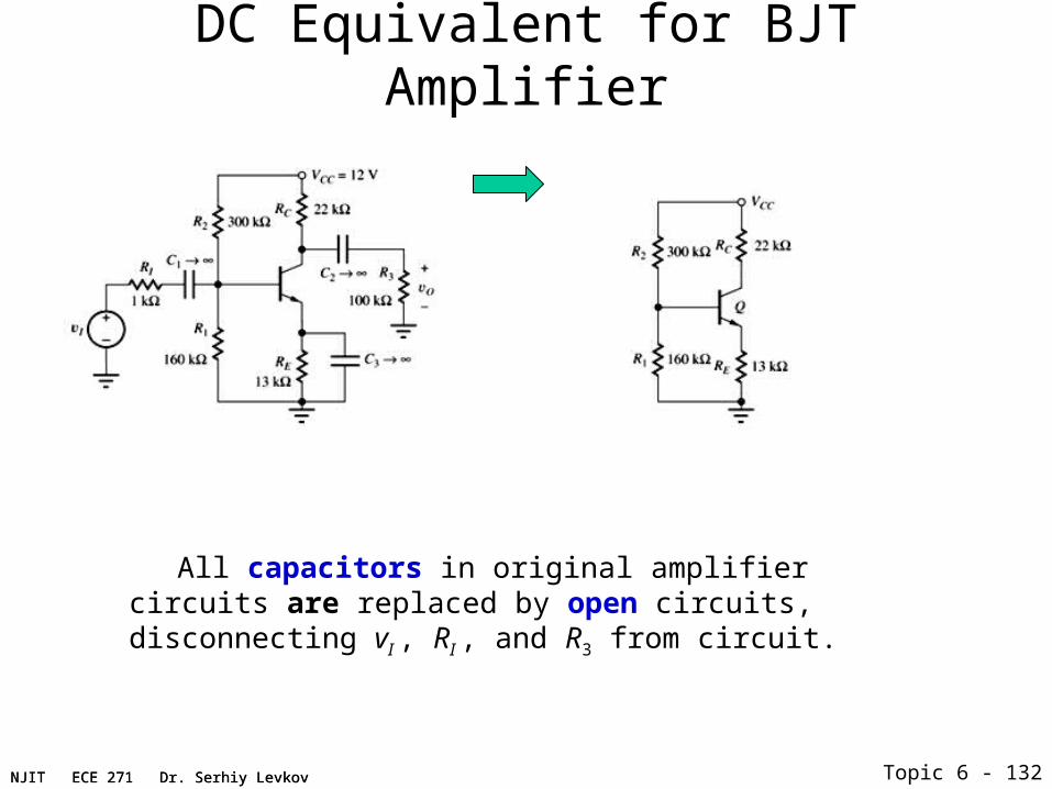
DC Equivalent for BJT Amplifier
All capacitors in original amplifier circuits need to be replaced by open circuits, disconnecting vI , RI , and R3 from circuit.

NJIT ECE 271 Dr. Serhiy Levkov Topic 6 - 131NJIT ECE 271 Dr. Serhiy Levkov
DC Equivalent for BJT Amplifier
All capacitors in original amplifier circuits need to be replaced by open circuits, disconnecting vI , RI , and R3 from circuit.
NJIT ECE 271 Dr. Serhiy Levkov Topic 6 - 132NJIT ECE 271 Dr. Serhiy Levkov
DC Equivalent for BJT Amplifier
All capacitors in original amplifier circuits are replaced by open circuits, disconnecting vI , RI , and R3 from circuit.

NJIT ECE 271 Dr. Serhiy Levkov Topic 6 - 133NJIT ECE 271 Dr. Serhiy Levkov
AC Equivalent for BJT Amplifier
Make ac equivalent circuit by replacing all- capacitors by short circuits - inductors by open circuits - dc voltage sources by ground connections - dc current sources by open circuits

NJIT ECE 271 Dr. Serhiy Levkov Topic 6 - 134NJIT ECE 271 Dr. Serhiy Levkov
AC Equivalent for BJT Amplifier
Simplify the ac equivalent circuit

NJIT ECE 271 Dr. Serhiy Levkov Topic 6 - 135NJIT ECE 271 Dr. Serhiy Levkov
AC Equivalent for BJT Amplifier
Simplify the ac equivalent circuit

NJIT ECE 271 Dr. Serhiy Levkov Topic 6 - 136NJIT ECE 271 Dr. Serhiy Levkov
AC Equivalent for BJT Amplifier
21
3
160k 300k
22k 100kB
L C
R R R
R R R

NJIT ECE 271 Dr. Serhiy Levkov Topic 6 - 137NJIT ECE 271 Dr. Serhiy Levkov
Small-Signal Modeling
• For AC analysis (or general time varying analysis) we would need to use phasor , time domain, Laplace Transform (or similar) methods.
• Those are working better with linear systems.
• Need to make the linear model – small signal model.
• Assume that the time varying components are small signals and construct the two port model, which is linear.
• The concept of small signal is device dependent.
• We start from developing small signal model for a diode and then switch to transistor
NJIT ECE 271 Dr. Serhiy Levkov Topic 6 - 138NJIT ECE 271 Dr. Serhiy Levkov
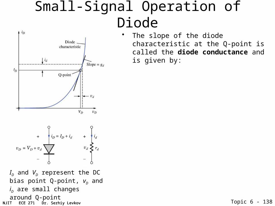
Small-Signal Operation of Diode• The slope of the diode characteristic at the Q-
point is called the diode conductance and is given by:
ID and VD represent the DC bias point Q-point, vD and iD are small changes around Q-point

NJIT ECE 271 Dr. Serhiy Levkov Topic 6 - 139NJIT ECE 271 Dr. Serhiy Levkov
Small-Signal Operation of Diode• The slope of the diode characteristic at the Q-
point is called the diode conductance and is given by:
• gd is small but non-zero for ID = 0 because slope of diode equation is nonzero at the origin.
exp 1
exp 1 1
exp
40 for 0.025V
D D S DSd
T T TDD Qp
DS D
TT
S
D S
T
D Dd D
T
vI
Vv
v
V
i I vg
V Vv
I iV V
ig
I
Ii IV
i
ID and VD represent the DC bias point Q-point, vD and iD are small changes around Q-point
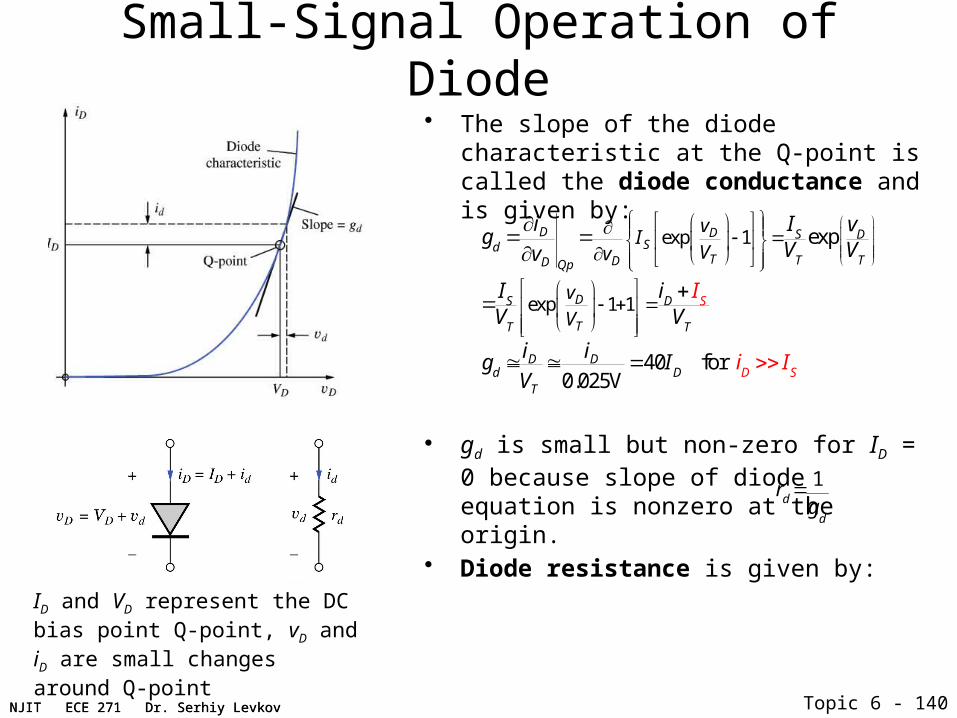
NJIT ECE 271 Dr. Serhiy Levkov Topic 6 - 140NJIT ECE 271 Dr. Serhiy Levkov
Small-Signal Operation of Diode• The slope of the diode characteristic at the Q-
point is called the diode conductance and is given by:
• gd is small but non-zero for ID = 0 because slope of diode equation is nonzero at the origin.
• Diode resistance is given by:
exp 1
exp 1 1
exp
40 for 0.025V
D D S DSd
T T TDD Qp
DS D
TT
S
D S
T
D Dd D
T
vI
Vv
v
V
i I vg
V Vv
I iV V
ig
I
Ii IV
i
rd 1
gd
ID and VD represent the DC bias point Q-point, vD and iD are small changes around Q-point

• The slope of the diode characteristic at the Q-point is called the diode conductance and is given by:
• gd is small but non-zero for ID = 0 because slope of diode equation is nonzero at the origin.
• Diode resistance is given by:
• Thus, linear model in the vicinity of ID :
when
NJIT ECE 271 Dr. Serhiy Levkov Topic 6 - 141NJIT ECE 271 Dr. Serhiy Levkov
Small-Signal Operation of Diode
exp 1
exp 1 1
exp
40 for 0.025V
D D S DSd
T T TDD Qp
DS D
TT
S
D S
T
D Dd D
T
vI
Vv
v
V
i I vg
V Vv
I iV V
ig
I
Ii IV
i
rd 1
gd
ID and VD represent the DC bias point Q-point, vD and iD are small changes around Q-point
, small signal model D dd dD d
i g vi I i
vd2V
T0.05V or v
d5 mV

NJIT ECE 271 Dr. Serhiy Levkov Topic 6 - 142NJIT ECE 271 Dr. Serhiy Levkov
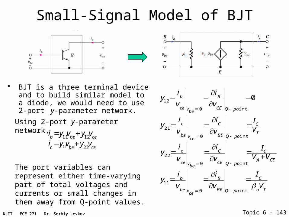
• BJT is a three terminal device and to build similar model to a diode, we would need to use 2-port y-parameter network.
Small-Signal Model of BJT
Using 2-port y-parameter network,
The port variables can represent either time-varying part of total voltages and currents or small changes in them away from Q-point values.
ib y
11v
be y
12v
ce
ic y21vbe
y22
vce
y12
ib
vce v
be0
i
B
vCE Q point
0
y21
ic
vbe v
ce0
i
C
vBE Q point
IC
VT
y22
ic
vce v
be0
i
C
vCE Q point
IC
VAV
CE
y11
ib
vbe v
ce0
i
B
vBE Q point
I
C
oV
T
NJIT ECE 271 Dr. Serhiy Levkov Topic 6 - 143NJIT ECE 271 Dr. Serhiy Levkov
Small-Signal Model of BJT
y12
ib
vce v
be0
i
B
vCE Q point
0
y21
ic
vbe v
ce0
i
C
vBE Q point
IC
VT
y22
ic
vce v
be0
i
C
vCE Q point
IC
VAV
CE
y11
ib
vbe v
ce0
i
B
vBE Q point
I
C
oV
T
• BJT is a three terminal device and to build similar model to a diode, we would need to use 2-port y-parameter network.
Using 2-port y-parameter network,
The port variables can represent either time-varying part of total voltages and currents or small changes in them away from Q-point values.
ib y
11v
be y
12v
ce
ic y21vbe
y22
vce

NJIT ECE 271 Dr. Serhiy Levkov Topic 6 - 144NJIT ECE 271 Dr. Serhiy Levkov
Small Signal Hybrid-Pi Model of BJT
• The hybrid-pi small-signal model is most widely accepted model for BJT amplifier.
• Small-signal parameters are controlled by the Q-point

NJIT ECE 271 Dr. Serhiy Levkov Topic 6 - 145NJIT ECE 271 Dr. Serhiy Levkov
Small Signal Hybrid-Pi Model of BJT
• The hybrid-pi small-signal model is most widely accepted model for BJT amplifier.
• Small-signal parameters are controlled by the Q-point
• VA - Early Voltage
Trans-conductance:
21
1 40Cm C
Ty
Ig IV
Input resistance:
11
1 o o T
m Cy
Vrg I
Output resistance:
ro 1
y22
V
AV
CE
IC
V
A
IC

NJIT ECE 271 Dr. Serhiy Levkov Topic 6 - 146NJIT ECE 271 Dr. Serhiy Levkov
Small Signal Hybrid-Pi Model of BJT
Trans-conductance:
| 40CCm Q C
BE T
i
v
Ig IV
Input resistance:
o o T
m C
Vrg I
Output resistance:
ro 1
y22
V
AV
CE
IC
V
A
IC
bo is the small-signal common-emitter current gain of the BJT.
• The hybrid-pi small-signal model is most widely accepted model for BJT amplifier.
• Small-signal parameters are controlled by the Q-point
• VA - Early Voltage

NJIT ECE 271 Dr. Serhiy Levkov Topic 6 - 147NJIT ECE 271 Dr. Serhiy Levkov
Small Signal Hybrid-Pi Model of BJT
Trans-conductance:
| 40CCm Q C
BE T
i
v
Ig IV
Input resistance:
o o T
m C
Vrg I
Output resistance:
ro 1
y22
V
AV
CE
IC
V
A
IC
2 0.005be T be
v V or v V
Definition of small signal for BJT:
bo is the small-signal common-emitter current gain of the BJT.
• The hybrid-pi small-signal model is most widely accepted model for BJT amplifier.
• Small-signal parameters are controlled by the Q-point
• VA - Early Voltage

NJIT ECE 271 Dr. Serhiy Levkov Topic 6 - 148NJIT ECE 271 Dr. Serhiy Levkov
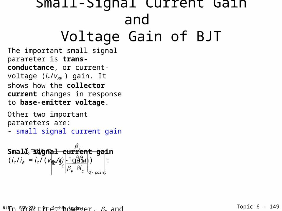
Small-Signal Current Gain and Voltage Gain of BJT
The important small signal parameter is trans-conductance, or current-voltage (iC/vBE ) gain. It shows how the collector current changes in response to base-emitter voltage.
NJIT ECE 271 Dr. Serhiy Levkov Topic 6 - 149NJIT ECE 271 Dr. Serhiy Levkov
Small-Signal Current Gain and Voltage Gain of BJT
The important small signal parameter is trans-conductance, or current-voltage (iC/vBE ) gain. It shows how the collector current changes in response to base-emitter voltage.
Other two important parameters are: - small signal current gain
Small signal current gain (iC/iB = iC/(vBE /r) - gain) :
In practice, however, bF and bo are often assumed to be equal.
og
mr
F
1 IC
1
F
F
iC
Q point

NJIT ECE 271 Dr. Serhiy Levkov Topic 6 - 150NJIT ECE 271 Dr. Serhiy Levkov
Small-Signal Current Gain and Voltage Gain of BJT
The important small signal parameter is trans-conductance, or current-voltage (iC/vBE ) gain. It shows how the collector current changes in response to base-emitter voltage.
Other two important parameters are: - small signal current gain - intrinsic voltage gain
Small signal current gain (iC/iB = iC/(vBE /r) - gain) :
In practice, however, bF and bo are often assumed to be equal.
Intrinsic voltage gain (vCE/vBE – gain) :
For VCE << VA,
mF represents maximum voltage gain individual BJT can provide, doesn’t change with operating point, and ranges from 1000 to 4000.
Small signal model for pnp-BJT is similar
F
VA
VT
40VA
og
mr
F
1 IC
1
F
F
iC
Q point
F gmro
I
C
VT
VA V
CEIC
V
A V
CE
VT

NJIT ECE 271 Dr. Serhiy Levkov Topic 6 - 151NJIT ECE 271 Dr. Serhiy Levkov
Using 2-port y-parameter network,
The port variables can represent either time-varying part of total voltages and currents or small changes in them away from Q-point values.
ig y
11v
gs y
12v
ds
id y
21v
gs y
22v
ds
y11
ig
vgs v
ds0
i
G
vGS Q point
0
y12
ig
vds v
gs0
i
G
vDS Q point
0
y21
id
vgs v
ds0
i
D
vGS Q point
2ID
VGS V
TN
y22
id
vds v
gs0
i
D
vDS Q point
ID
1V
DS
Small-Signal Model of MOSFET (nmos)

NJIT ECE 271 Dr. Serhiy Levkov Topic 6 - 152NJIT ECE 271 Dr. Serhiy Levkov
Using 2-port y-parameter network,
The port variables can represent either time-varying part of total voltages and currents or small changes in them away from Q-point values.
ig y
11v
gs y
12v
ds
id y
21v
gs y
22v
ds
y11
ig
vgs v
ds0
i
G
vGS Q point
0
y12
ig
vds v
gs0
i
G
vDS Q point
0
y21
id
vgs v
ds0
i
D
vGS Q point
2ID
VGS V
TN
y22
id
vds v
gs0
i
D
vDS Q point
ID
1V
DS
Small-Signal Model of MOSFET (nmos)

NJIT ECE 271 Dr. Serhiy Levkov Topic 6 - 153NJIT ECE 271 Dr. Serhiy Levkov
Small-Signal Model of MOSFET (nmos)
• Since gate is insulated from channel by gate-oxide input resistance of transistor is infinite.
• Small-signal parameters are controlled by the Q-point.
• For same operating point, MOSFET has higher transconductance and lower output resistance that BJT.
Trans-conductance:
21
2 2Dn Dm
GS TN
Ig y K IV V
Output resistance:
22
1/1 1DSo
D D
Vry I I
Amplification factor (intrinsic voltage gain) for lVDS<<1:
Where l – channel-length modulation parameter.
)/2
21/ 1(
DS nf m o
DGS TNV
KVg rIV
Definition of small signal for MOSFET:
0.2 GS TNgsv V V

NJIT ECE 271 Dr. Serhiy Levkov Topic 6 - 154NJIT ECE 271 Dr. Serhiy Levkov
Small-Signal Model of JFET
1r
g
y11i
G
vGS Q point
I
GI
SG
VT
0 for IG0
gmy
21i
D
vGS Q point
ID
VGS V
P2
gm2 I
DSS
VP2
(VGS V
P)
1r
o
y22i
D
vDS Q point
ID
1V
DS
iDI
DSS1
vGS
VP
2
1vDS
for vDSv
GS V
P
iGI
SGexp
vGS
VT
1

NJIT ECE 271 Dr. Serhiy Levkov Topic 6 - 155NJIT ECE 271 Dr. Serhiy Levkov
Small-Signal Model of JFET
Since JFET is normally operated with gate junction reverse-biased,
IG ISG
rg
For small-signal operation, the input signal limit is:
The amplification factor is given by:
vgs 0.2 V
GS V
P
f g
mr
o 2
1 V
DS
VGS V
P
2V
P
IDSSI
D

NJIT ECE 271 Dr. Serhiy Levkov Topic 6 - 156NJIT ECE 271 Dr. Serhiy Levkov
Summary of FET and BJT Small-Signal Models
NJIT ECE 271 Dr. Serhiy Levkov Topic 6 - 157NJIT ECE 271 Dr. Serhiy Levkov
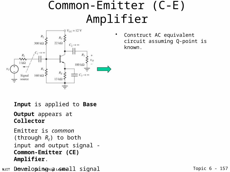
Common-Emitter (C-E) Amplifier
• Construct AC equivalent circuit assuming Q-point is known.
Input is applied to Base
Output appears at Collector
Emitter is common (through RE) to both input and output signal - Common-Emitter (CE) Amplifier.
Developing a small signal model:

NJIT ECE 271 Dr. Serhiy Levkov Topic 6 - 158NJIT ECE 271 Dr. Serhiy Levkov
Common-Emitter (C-E) Amplifier
• Construct AC equivalent circuit assuming Q-point is known.
• Use the small signal hybrid model for BJT
NJIT ECE 271 Dr. Serhiy Levkov Topic 6 - 159NJIT ECE 271 Dr. Serhiy Levkov
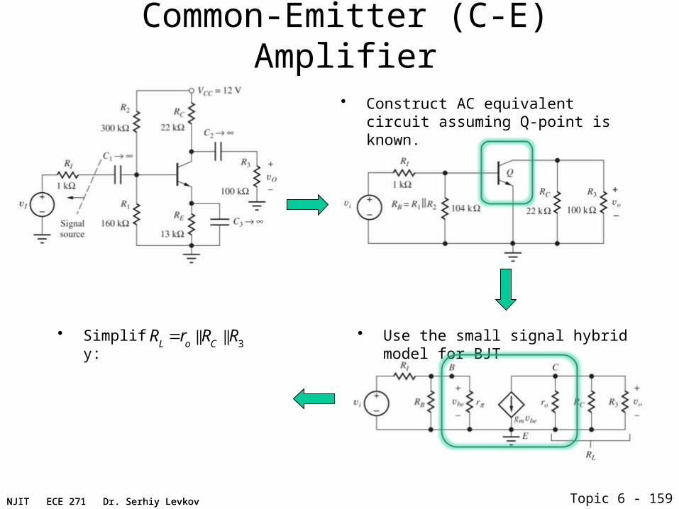
Common-Emitter (C-E) Amplifier
• Construct AC equivalent circuit assuming Q-point is known.
• Use the small signal hybrid model for BJT3
|| ||L o C
R r R R• Simplify:

NJIT ECE 271 Dr. Serhiy Levkov Topic 6 - 160NJIT ECE 271 Dr. Serhiy Levkov
Common-Emitter (C-E) Amplifier
• Construct AC equivalent circuit assuming Q-point is known.
3|| ||
L o CR r R R • Use the small signal hybrid model for BJT• Simplify:

NJIT ECE 271 Dr. Serhiy Levkov Topic 6 - 161NJIT ECE 271 Dr. Serhiy Levkov
C-E Amplifier – Voltage Gain
• Goal – develop the overall voltage gain from vi to vo - Av
CE .

NJIT ECE 271 Dr. Serhiy Levkov Topic 6 - 162NJIT ECE 271 Dr. Serhiy Levkov
C-E Amplifier – Voltage Gain
• Goal – develop the overall voltage gain from vi to vo - Av
CE .
•
where - terminal gain -
gain between transistor terminals.
v v v vCE CEo o b bA Av vtv v v v
i b i i
vCE oAvt v
b
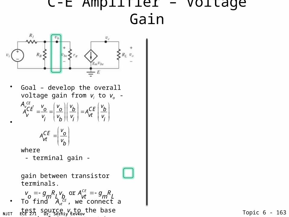
NJIT ECE 271 Dr. Serhiy Levkov Topic 6 - 163NJIT ECE 271 Dr. Serhiy Levkov
C-E Amplifier – Voltage Gain
• Goal – develop the overall voltage gain from vi to vo - Av
CE .
•
where - terminal gain -
gain between transistor terminals.
• To find AvtCE , we connect a test source vb
to the base terminal (right circuit):
v v v vCE CEo o b bA Av vtv v v v
i b i i
vCE oAvt v
b
or CEv g R v A g Ro m L b vt m L

NJIT ECE 271 Dr. Serhiy Levkov Topic 6 - 164NJIT ECE 271 Dr. Serhiy Levkov
C-E Amplifier – Voltage Gain
• Goal – develop the overall voltage gain from vi to vo - Av
CE .
•
where - terminal gain -
gain between transistor terminals.
• To find AvtCE , we connect a test source vb
to the base terminal (right circuit):
v v v vCE CEo o b bA Av vtv v v v
i b i i
vCE oAvt v
b
• For the input resistance RiB :
or CEv g R v A g Ro m L b vt m L
b
b
vR r
iB i

NJIT ECE 271 Dr. Serhiy Levkov Topic 6 - 165NJIT ECE 271 Dr. Serhiy Levkov
C-E Amplifier – Voltage Gain
• Goal – develop the overall voltage gain from vi to vo - Av
CE .
•
where - terminal gain -
gain between transistor terminals.
• To find AvtCE , we connect a test source vb
to the base terminal (right circuit):
v v v vCE CEo o b bA Av vtv v v v
i b i i
vCE oAvt v
b
• For the input resistance RiB :
or CEv g R v A g Ro m L b vt m L
b
b
vR r
iB i
|| Now, since ,
||
we have
||
||CE CE b Bv vt m L
i
B ibb i
I B ib
I B
v R rA A g
R Rv v
Rv R
R R R
R r

NJIT ECE 271 Dr. Serhiy Levkov Topic 6 - 166NJIT ECE 271 Dr. Serhiy Levkov
C-E Amplifier – Voltage Gain
• Goal – develop the overall voltage gain from vi to vo - Av
CE .
•
where - terminal gain -
gain between transistor terminals.
• To find AvtCE , we connect a test source vb
to the base terminal (right circuit):
v v v vCE CEo o b bA Av vtv v v v
i b i i
vCE oAvt v
b
• For the input resistance RiB :
• We see that the overall voltage gain is the terminal gain reduced by the voltage division between R1 and equivalent resistance at the base.
• Thus AvtCE is the upper limit of voltage
gain.or CEv g R v A g R
o m L b vt m L
b
b
vR r
iB i
|| Now, since ,
||
we have
||
||CE CE b Bv vt m L
i
B ibb i
I B ib
I B
v R rA A g
R Rv v
Rv R
R R R
R r
NJIT ECE 271 Dr. Serhiy Levkov Topic 6 - 167NJIT ECE 271 Dr. Serhiy Levkov
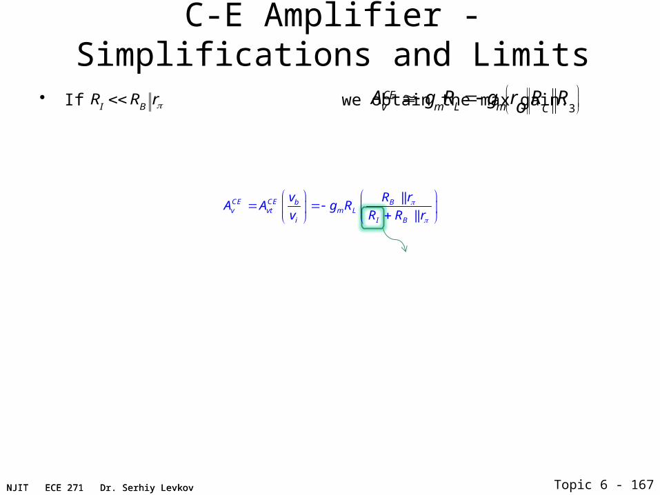
C-E Amplifier - Simplifications and Limits
• If we obtain the max gain: I B
R R r
AvCE g
mR
L g
mro R
CR
3
||
||CE CE b Bv vt m L
i I B
v R rA A g R
v R R r

NJIT ECE 271 Dr. Serhiy Levkov Topic 6 - 168NJIT ECE 271 Dr. Serhiy Levkov
C-E Amplifier - Simplifications and Limits
• If we obtain the max gain:
• For maximum gain we set R3 >> RC and RC << rO . . If we assume IC RC = VCC with 0 < < 1:
I B
R R r
AvCE g
mR
L g
mro R
CR
3
40Cv vt
CCm
TC C
Ig RA A RV
V
cRRRor C
3
||
||CE CE b Bv vt m L
i I B
v R rA A g R
v R R r

NJIT ECE 271 Dr. Serhiy Levkov Topic 6 - 169NJIT ECE 271 Dr. Serhiy Levkov
C-E Amplifier - Simplifications and Limits
• If we obtain the max gain:
• For maximum gain we set R3 >> RC and RC << ro . . If we assume IC RC = VCC with 0 < < 1:
Typically, = 1/3, since common design allocates one-third power supply across RC. To further account for other approximations leading to this result, we use:
I B
R R r
AvCE g
mR
L g
mro R
CR
3
40Cv vt
CCm
TC C
Ig RA A RV
V
10v CC
A V
cRRRor C
3

NJIT ECE 271 Dr. Serhiy Levkov Topic 6 - 170NJIT ECE 271 Dr. Serhiy Levkov
C-E Amplifier - Simplifications and Limits
• If we obtain the max gain:
• For maximum gain we set R3 >> RC and RC << ro . . If we assume IC RC = VCC with 0 < < 1:
Typically, = 1/3, since common design allocates one-third power supply across RC. To further account for other approximations leading to this result, we use:
• Also, if the load resistor approaches ro (RC and R3 are very large), voltage gain is limited by amplification factor, mf , of BJT itself.
• For large RE, voltage gain can be approximated as:
I B
R R r
AvCE g
mR
L g
mro R
CR
3
40Cv vt
CCm
TC C
Ig RA A RV
V
10v CC
A V
AvtCE
gmRL
1gmRE
R
LR
E
cRRRor C
3

NJIT ECE 271 Dr. Serhiy Levkov Topic 6 - 171NJIT ECE 271 Dr. Serhiy Levkov
C-E Amplifier – Example
• Problem: Find voltage gain, input and output resistances.
• Given data: bF = 65, VA = 50 V• Assumptions: Active-region
operation, VBE = 0.7 V, small signal operating conditions.
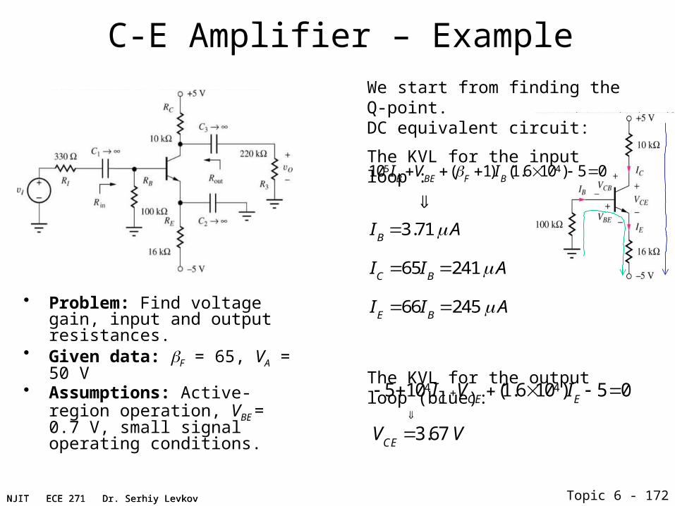
NJIT ECE 271 Dr. Serhiy Levkov Topic 6 - 172NJIT ECE 271 Dr. Serhiy Levkov
C-E Amplifier – Example
• Problem: Find voltage gain, input and output resistances.
• Given data: bF = 65, VA = 50 V• Assumptions: Active-region
operation, VBE = 0.7 V, small signal operating conditions.
We start from finding the Q-point. DC equivalent circuit:
The KVL for the input loop :
The KVL for the output loop (blue):
5 410 ( 1) (1.6 10 ) 5 0B BE F B
I V I
3.71
65 241
66 245
B
C B
E B
I A
I I A
I I A
4 45 10 (1.6 10 ) 5 0
3.67
C CE E
CE
I V I
V V

NJIT ECE 271 Dr. Serhiy Levkov Topic 6 - 173NJIT ECE 271 Dr. Serhiy Levkov
C-E Amplifier – Example
Next we construct the ac equivalent and simplify it.
gm 40I
C 9.64 10 3 S
r
oV
T
IC
6.64 k
ro
VA V
CE
IC
223 k
Rin R
Br 6.23 k
RoutR
Cr
o9.57 k
Av
vo
vi
gm(R
outR
3)
Rin
RIR
in
84.0

NJIT ECE 271 Dr. Serhiy Levkov Topic 6 - 174NJIT ECE 271 Dr. Serhiy Levkov
Common-Source Amplifier
• Construct AC equivalent circuit.• Assume that Q-point is known.

NJIT ECE 271 Dr. Serhiy Levkov Topic 6 - 175NJIT ECE 271 Dr. Serhiy Levkov
Common-Source Amplifier
• Construct AC equivalent circuit.• Assume that Q-point is known.
• Use the small signal hybrid model for BJT

NJIT ECE 271 Dr. Serhiy Levkov Topic 6 - 176NJIT ECE 271 Dr. Serhiy Levkov
Common-Source Amplifier
• Construct AC equivalent circuit.• Assume that Q-point is known.
• Use the small signal hybrid model for MOSFET3
|| ||L o C
R r R R• Simplify:

NJIT ECE 271 Dr. Serhiy Levkov Topic 6 - 177NJIT ECE 271 Dr. Serhiy Levkov
Common-Source Amplifier
• Construct AC equivalent circuit.• Assume that Q-point is known.
• Use the small signal model3
|| ||L o C
R r R R• Simplify:

NJIT ECE 271 Dr. Serhiy Levkov Topic 6 - 178NJIT ECE 271 Dr. Serhiy Levkov
C-S Amplifier - Terminal Voltage Gain
Terminal voltage gain between gate and drain:
Overall voltage gain from source vi to output voltage across R3
Avtv
dv
gv
ov
gs g
mR
L
gs gso ov vt
i gs i i
Gv m L
I G
v vv vA Av v v v
RA g R
R R
Voltage division

NJIT ECE 271 Dr. Serhiy Levkov Topic 6 - 179NJIT ECE 271 Dr. Serhiy Levkov
C-S Amplifier - Simplifications
• If we assume RI << RG
• Generally R3 >> RD and RD << ro. Hence, total load resistance on drain is RD. For this case, common design allocates half the power supply for voltage drop across RD and (VGS - VTN ) = 1V
• Also, if load resistor approaches ro, (RD and R3 are very large), voltage gain is limited by amplification factor, mf of the MOSFET itself.
AvA
vt g
mR
L g
mr
oR
DR
3
This implies that total signal voltage at input appears across gate-source terminals.
Av g
mR
D
IDR
D
VGS V
TN
2
VDD

NJIT ECE 271 Dr. Serhiy Levkov Topic 6 - 180NJIT ECE 271 Dr. Serhiy Levkov
C-S Amplifier - Input and Output Resistance
• Input resistance of C-S amplifier is much larger than that of corresponding C-E amplifier.
vxi
xR
G
RinR
G
• For comparable bias points, output resistances of C-S and C-E amplifiers are similar.
for xoout D D o D
x
vR R r R r Ri
In this case, vgs= 0.

NJIT ECE 271 Dr. Serhiy Levkov Topic 6 - 181NJIT ECE 271 Dr. Serhiy Levkov
C-S Amplifier - Example
• Problem: Find voltage gain, input and output resistances.
• Given data: Kn = 500 mA/V2, VTN = 1V, l = 0.0167 V-1
Do example on the board

NJIT ECE 271 Dr. Serhiy Levkov Topic 6 - 182NJIT ECE 271 Dr. Serhiy Levkov
C-S Amplifier - Example
• Problem: Find voltage gain, input and output resistances.
• Given data: Kn = 500 mA/V2, VTN = 1V, l = 0.0167 V-1
Construct dc equivalent circuit
1 6,
Since 0,
5 10
G
DS
IVI
41
2
10 2 10 ( ) 0
(0.4 )2
5 , 2 ,
250
DS D
nD DS TN
DS GS
D
V I IK
I V V
V V V V
I A
KVL:

NJIT ECE 271 Dr. Serhiy Levkov Topic 6 - 183NJIT ECE 271 Dr. Serhiy Levkov
Next we construct the ac equivalent and simplify it.
RinR
G1R
G21 M
3( ) 7.93ino
v m outI ini
RvA g R RR Rv
gm 2K
nI
DS(1V
DS)5.20104 S
ro
1VDS
ID
260 k
C-S Amplifier - Example
3 18.2 o Gout DR r R R k
GIR R

NJIT ECE 271 Dr. Serhiy Levkov Topic 6 - 184NJIT ECE 271 Dr. Serhiy Levkov
Summary of CE / CS Amplifiers