Nitrides on Si(111) substrates for use in nonlinear optical devices · PDF file ·...
6
A4.5 Schaadt 1 Subproject A4.5 Nitrides on Si(111) substrates for use in nonlinear optical devices Principle Investigator: Daniel Schaadt CFN-Financed Scientists: P. Ganz (1/2 E13, 14 months) Further Scientist: Dr. Dongzhi Hu DFG-Center for Functional Nanostructures/Institut für Angewandte Physik Karlsruhe Institute of Technology (KIT)
Transcript of Nitrides on Si(111) substrates for use in nonlinear optical devices · PDF file ·...
A4.5 Schaadt
1
Subproject A4.5
Nitrides on Si(111) substrates for use in nonlinear optical devices Principle Investigator: Daniel Schaadt CFN-Financed Scientists: P. Ganz (1/2 E13, 14 months) Further Scientist: Dr. Dongzhi Hu DFG-Center for Functional Nanostructures/Institut für Angewandte Physik Karlsruhe Institute of Technology (KIT)
A4.5 Schaadt
2
Nitrides on Si(111) substrates for use in nonlinear optical devices Introduction and Summary Next-generation fiber-optic communication networks are supposed to work with data rates of over 100 Gb/s, which requires the development of fast optical devices such as (de)multiplexers, modulators and wavelength converters. For realistic commercial use, these devices must be compatible with current CMOS technology for high integration and cheap to produce, which requires the use of Si-based devices. A promising approach is the use of Si on insulator based waveguide structures, which are combined with a nonlinear material. Using this idea, a record-breaking ultra-fast demultiplexer achieving very high conversion rates from 170 Gbit/s to 42.5 Gbit/s was implemented previously by the groups of J. Leuthold and W. Freude.[1] Similar approaches might be used for electro-optical modulators and switches, which are investigated in subproject A4.4. For these devices, a highly-nonlinear electro-optic active material is required. In very close collaboration with A4.4, we explore nitrides, in particular AlN and GaN/AlN quantum wells, as possible non-linear active media.
AlN in its stable wurtzite structure configuration has a bandgap of 6.2 eV and is therefore transparent at wavelength of interest for signal transmission through optical fibers. In addition, it’s second order optical properties with a nonlinear coefficient d33 = 11 pm/V[2] make it interesting for use in electro-optical modulators based on slot waveguides filled with non-linear material. While nitrides can be easily grown on highly lattice-matched substrates, such as 6H-SiC or LiAlO2,[3] the growth on Si substrates is difficult due to large differences in the crystal structure and the thermal constants. Several attempts have been presented for nitrides growth on Si(111).[4] Thereby AlN was used as wetting and buffer layer for the subsequent growth of GaN and InN layers. And Little attention was given to the optical properties of AlN itself. In this project, we first study growth of vetical AlN films. This is the base step for later to place AlN into a slot waveguide structure and growt GaN/AlN quantum well structures. We have therefore started to perform a careful analysis of the growth parameters and their influence on the properties of AlN deposited on Si(111) planar substrates.
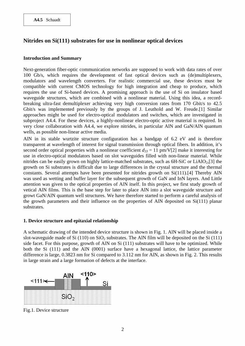
1. Device structure and epitaxial relationship A schematic drawing of the intended device structure is shown in Fig. 1. AlN will be placed inside a slot-waveguide made of Si (110) on SiO2 substrates. The AlN film will be deposited on the Si (111) side facet. For this purpose, growth of AlN on Si (111) substrates will have to be optimized. While both the Si (111) and the AlN (0001) surface have a hexagonal lattice, the lattice parameter difference is large, 0.3823 nm for Si compared to 3.112 nm for AlN, as shown in Fig. 2. This results in large strain and a large formation of defects at the interface.
Fig.1. Device structure
A4.5 Schaadt
3
AlN
a = 0.3112 nm c = 0.4982 nm
Si
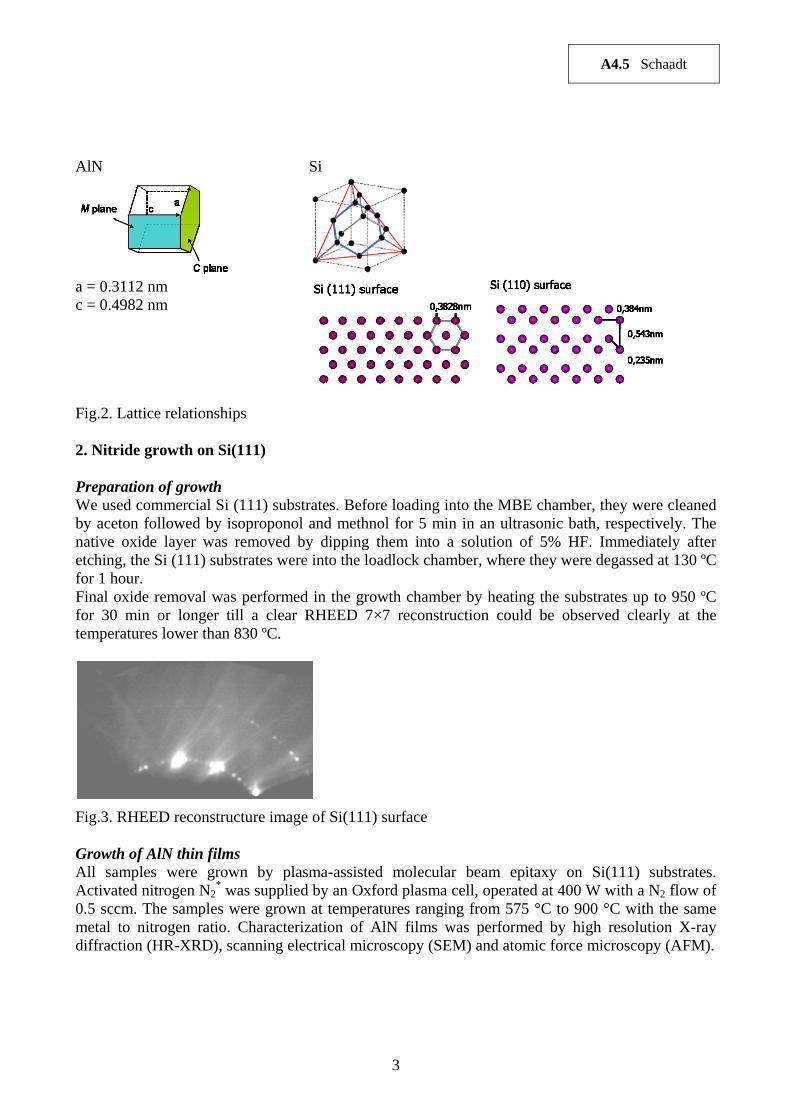
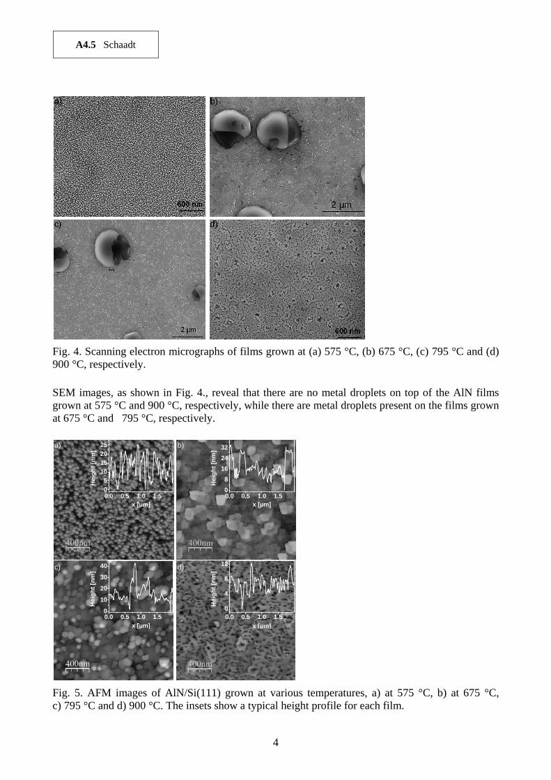
Fig.2. Lattice relationships 2. Nitride growth on Si(111) Preparation of growth We used commercial Si (111) substrates. Before loading into the MBE chamber, they were cleaned by aceton followed by isoproponol and methnol for 5 min in an ultrasonic bath, respectively. The native oxide layer was removed by dipping them into a solution of 5% HF. Immediately after etching, the Si (111) substrates were into the loadlock chamber, where they were degassed at 130 ºC for 1 hour. Final oxide removal was performed in the growth chamber by heating the substrates up to 950 ºC for 30 min or longer till a clear RHEED 7×7 reconstruction could be observed clearly at the temperatures lower than 830 ºC.
Fig.3. RHEED reconstructure image of Si(111) surface Growth of AlN thin films All samples were grown by plasma-assisted molecular beam epitaxy on Si(111) substrates. Activated nitrogen N2
* was supplied by an Oxford plasma cell, operated at 400 W with a N2 flow of 0.5 sccm. The samples were grown at temperatures ranging from 575 °C to 900 °C with the same metal to nitrogen ratio. Characterization of AlN films was performed by high resolution X-ray diffraction (HR-XRD), scanning electrical microscopy (SEM) and atomic force microscopy (AFM).
A4.5 Schaadt
4
Fig. 4. Scanning electron micrographs of films grown at (a) 575 °C, (b) 675 °C, (c) 795 °C and (d) 900 °C, respectively.
SEM images, as shown in Fig. 4., reveal that there are no metal droplets on top of the AlN films grown at 575 °C and 900 °C, respectively, while there are metal droplets present on the films grown at 675 °C and 795 °C, respectively.
Fig. 5. AFM images of AlN/Si(111) grown at various temperatures, a) at 575 °C, b) at 675 °C, c) 795 °C and d) 900 °C. The insets show a typical height profile for each film.
0.0 0.5 1.0 1.50
5
10
15
20
25
Hei
gh
t [n
m]
x [µm]0.0 0.5 1.0 1.50
8
16
24
32
Hei
gh
t [n
m]
x [µm]
0.0 0.5 1.0 1.50
10
20
30
40
Hei
gh
t [n
m]
x [µm]
0.0 0.5 1.0 1.50
4
8
12
Hei
gh
t [n
m]
x [µm]
a) b)
c) d)
A4.5 Schaadt
5
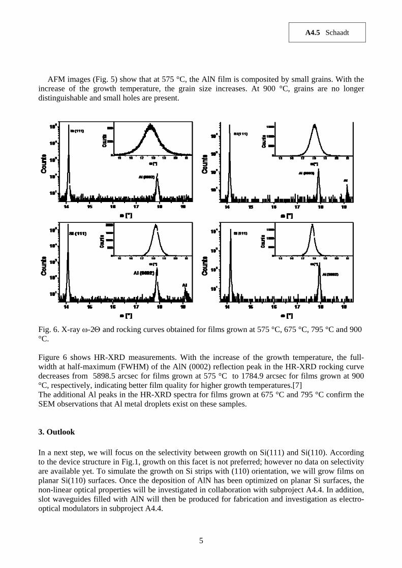
AFM images (Fig. 5) show that at 575 °C, the AlN film is composited by small grains. With the increase of the growth temperature, the grain size increases. At 900 °C, grains are no longer distinguishable and small holes are present.
Fig. 6. X-ray -2 and rocking curves obtained for films grown at 575 °C, 675 °C, 795 °C and 900 °C. Figure 6 shows HR-XRD measurements. With the increase of the growth temperature, the full-width at half-maximum (FWHM) of the AlN (0002) reflection peak in the HR-XRD rocking curve decreases from 5898.5 arcsec for films grown at 575 °C to 1784.9 arcsec for films grown at 900 °C, respectively, indicating better film quality for higher growth temperatures.[7] The additional Al peaks in the HR-XRD spectra for films grown at 675 °C and 795 °C confirm the SEM observations that Al metal droplets exist on these samples. 3. Outlook
In a next step, we will focus on the selectivity between growth on Si(111) and Si(110). According to the device structure in Fig.1, growth on this facet is not preferred; however no data on selectivity are available yet. To simulate the growth on Si strips with (110) orientation, we will grow films on planar Si(110) surfaces. Once the deposition of AlN has been optimized on planar Si surfaces, the non-linear optical properties will be investigated in collaboration with subproject A4.4. In addition, slot waveguides filled with AlN will then be produced for fabrication and investigation as electro-optical modulators in subproject A4.4.
A4.5 Schaadt
6
In addition to using AlN directly as a non-linear material, it’s large band gap and large band offsets compared to GaN allow the creation of intra-subband transitions at wavelengths interesting for optical fiber communication.[5] Very fast optical modulators and switches based on intra-subband transitions in nitrides have been recently published.[6] However, all devices were fabricated as strip-waveguides on expensive substrates, that are not compatible with current CMOS technology. We will attempt to fabricate similar device structures, composed of double quantum wells exploiting cross-tunneling and quantum confined Stark-Effect, on planar Si(111) substrates. In a first step, we will design appropriate film structures that compensate for the large lattice mismatch to the Si(111) substrates. In a second step, major issues to address will be interface roughness in the quantum wells, which can strongly affect the intended intra-subbband transition wavelength, and defect densities, which affects the non-radiative recombination and loss in the waveguide. Therefore, we will specifically focus on the optimization of the crystal structure of the active device region by appropriate buffer layer structures. Finally, we will produce strip waveguides for use as electro-optical modulators in subproject A4.4, provided the crystal structure can be optimized well enough to obtain transitions at the correct wavelength with low losses.
References [1] C. Koos, L. Jacome, C. Poulton, J. Leuthold, and W. Freude, Optics Express 15(10), 5976
(2007)
[2] M. C. M. C. Larciprete, A. Bosco, A. Belardini, R. Li Voti, G. Leahu, C. Sibilia, E. Fazio, R. Ostuni, M. Bertolotti, A. Passaseo, B. Potì, and Z. Del Prete, J. Appl. Phys. 100, 023507 (2006)
[3] e.g. D. M. Schaadt, O. Brandt, A. Trampert, H.-P. Schönherr and K. H. Ploog, "Epitaxial growth of 6H-AlN on M-plane 6H-SiC by molecular beam epitaxy," J. Crystal Growth 300(1), 127 (2007); I. Lo, C.-H. Hsieh, Y.-L. Chen, W.-Y. Pang, Y.-C. Hsu, J.-C. Chiang, M.-C. Chou, J.-K. Tsai, and D. M. Schaadt, "Line defects of M-plane GaN grown on gamma-LiAlO2 by plasma-assisted molecular beam epitaxy," Appl. Phys. Lett. 92, 202106 (2008)
[4] e.g. A. Sánchez-Garía, J. Ristic, E. Calleja, A. Perez-Rodriguez, C. Serre, A. Romano-Rodriguez, J. R. Morante, R. Koegler, W. Skorupa, A. Trampert, and K. H. Ploog, Phys. Stat. Sol. (a) 192(2), 401 (2002); S. Gwo, C.-L. Wu, C.-H. Shen, W.-H. Chang, T. M. Hsu, J.-S. Wang and J.-T. Hsu, Appl. Phys. Lett. 84, 19, 3765 (2004); X. H. Ji, S. P. Lau, H. Y. Yang, and Q. Y. Zhang, Thin Sol. Films 515, 4619 (2007)
[5] G. Chen, R. Rapaport, O. Mitrofanov, C. Gmachl, and H. M. Ng, Phys. Stat. Sol (b) 240(2), 384 (2003)
[6] e.g. N. Iizuka, K. Kaneko, and N. Suzuki, IEEE J. Quantum Elec. 42(8), 765 (2006); Y. Li, A. Bhattacharyya, Ch. Thomidis, T. D. Moustakas, and R. Paiella, Optics Express 15(26), 197922 (2007)
[7] D. Z. Hu, R. Vöhringer, and D. M. Schaadt, "Epitaxial growth of AlN films on Si (111)", AIP Conf. Proc. (2010) in print