Nitride layers grown on patterned graphene/ · PDF fileNitride layers grown on patterned...
2
Nitride layers grown on patterned graphene/SiC Authors: Bela Pecz (1), Andras Kovacs (2), Rafal E Dunin-Borkowski (2), Rositza Yakimova (3), Michael Heuken (4) 1. Thin Film Physics, MTA EK MFA, Budapest, HUNGARY 2. Ernst Ruska-Centre for Microscopy and Spectroscopy with Electrons and Peter Grünberg Institute, Forschungszentrum Jülich, Jülich, GERMANY 3. Department of Physics, Chemistry and Biology, Linköping University, S-581 83 Linköping, Linköping, SWEDEN 4. AIXTRON SE, Kaiserstrasse 98, 52134 Herzogenrath, GERMANY DOI: 10.1002/9783527808465.EMC2016.6338 Corresponding email: [email protected] Keywords: GaN, graphene, high power device Self-heating of high power GaN devices during their operation is a major drawback that limits the performance. Integration of sheets with very high thermal conductivity material could help in this matter. After some unsuccessful GaN growth experiments carried out directly on graphene, we succeeded to grow nitride layers on patterned graphene/6H-SiC by Metalorganic Chemical Vapour Deposition (MOCVD). The growth is similar to the well-known Epitaxial Lateral Overgrowth method in which the graphene buried stripes are overgrown laterally from the window regions, where AlN could grow on bare SiC with epitaxy. An AlN buffer layer was first deposited on patterned graphene/6H-SiC surface followed by a deposition of ~ 300 nm thick Al 0.2 Ga 0.8 N and ~ 1.5 µm thick GaN layer. The AlN buffer deposited onto the graphene stripe was grown in a 3D way (Fig.1a). The heterostructure was studied using aberration-corrected transmission electron microscopy (TEM) methods in combination of electron energy-loss X-ray spectroscopy (EDXS) and electron energy-loss spectroscopy (EELS). TEM specimens were prepared using both conventional and focused ion beam methods. The most surprising details of this study is the appearance of the AlN/GaN superlattices, which were formed in a self-organised way over the buffer layer. Instead the ternary AlGaN we have superlattice (Fig. 1.b and c) in which the thickness of the AlN/GaN is determined by the available elements from the Al 0.2 Ga 0.8 N which we wanted to grow. The control sample (without graphene) showed a much more flat AlN buffer and a ternary Al 0.2 Ga 0.8 N on that without any phase separation. EDXS mapping and also superlattice reflections show however, clearly the complete phase separation in the case the nitride layers are grown on graphene. We suppose, that some excess carbon induced the phase separation. The detailed TEM studies revealed the AlN nucleation directly on SiC and lateral overgrowth of graphene island as shown in Fig.2a. The high resolution image in Fig.2.b shows three layers of graphene and the AlN that is in epitaxy with SiC. Both interfaces are sharp and no interdiffusion of the elements are observed according to the Si, C (not shown) and Al maps in Fig. 2c The results show that high quality GaN layer over graphene/SiC can be grown with MOCVD that can serve as templates for high power GaN devices. Authors thank the support of the Hungarian National Scientific Foundation (OTKA) through Grant No. K 108869 and NN118914. B. P thanks to the European Commission for providing support to access the ER-C facility through the ESTEEM2 project. [1] A. Kovács, M. Duchamp, R.E. Dunin-Borkowski, R. Yakimova, P. L. Neumann, H. Behmenburg, B. Foltynski, C. Giesen, M. Heuken and B. Pécz, Advanced Materials Interfaces, published online: 22 DEC 2014 | DOI: 10.1002/admi.201400230, Vol. 2, Iss. 2, January 21 201597 630 Acknowledgements: References:
Transcript of Nitride layers grown on patterned graphene/ · PDF fileNitride layers grown on patterned...

Nitride layers grown on patterned graphene/SiC
Authors: Bela Pecz (1), Andras Kovacs (2), Rafal E Dunin-Borkowski (2), Rositza Yakimova (3),Michael Heuken (4)1. Thin Film Physics, MTA EK MFA, Budapest, HUNGARY2. Ernst Ruska-Centre for Microscopy and Spectroscopy with Electrons and Peter Grünberg Institute,Forschungszentrum Jülich, Jülich, GERMANY3. Department of Physics, Chemistry and Biology, Linköping University, S-581 83 Linköping, Linköping,SWEDEN4. AIXTRON SE, Kaiserstrasse 98, 52134 Herzogenrath, GERMANY
DOI: 10.1002/9783527808465.EMC2016.6338Corresponding email: [email protected]: GaN, graphene, high power device
Self-heating of high power GaN devices during their operation is a major drawback that limits the performance.Integration of sheets with very high thermal conductivity material could help in this matter. After someunsuccessful GaN growth experiments carried out directly on graphene, we succeeded to grow nitride layers onpatterned graphene/6H-SiC by Metalorganic Chemical Vapour Deposition (MOCVD). The growth is similar to thewell-known Epitaxial Lateral Overgrowth method in which the graphene buried stripes are overgrown laterallyfrom the window regions, where AlN could grow on bare SiC with epitaxy. An AlN buffer layer was firstdeposited on patterned graphene/6H-SiC surface followed by a deposition of ~ 300 nm thick Al0.2Ga0.8N and ~1.5 µm thick GaN layer. The AlN buffer deposited onto the graphene stripe was grown in a 3D way (Fig.1a). Theheterostructure was studied using aberration-corrected transmission electron microscopy (TEM) methods incombination of electron energy-loss X-ray spectroscopy (EDXS) and electron energy-loss spectroscopy (EELS).TEM specimens were prepared using both conventional and focused ion beam methods.The most surprising details of this study is the appearance of the AlN/GaN superlattices, which were formed in aself-organised way over the buffer layer. Instead the ternary AlGaN we have superlattice (Fig. 1.b and c) inwhich the thickness of the AlN/GaN is determined by the available elements from the Al0.2Ga0.8N which wewanted to grow. The control sample (without graphene) showed a much more flat AlN buffer and a ternary Al0.2
Ga0.8N on that without any phase separation. EDXS mapping and also superlattice reflections show however,clearly the complete phase separation in the case the nitride layers are grown on graphene. We suppose, thatsome excess carbon induced the phase separation.The detailed TEM studies revealed the AlN nucleation directly on SiC and lateral overgrowth of graphene islandas shown in Fig.2a. The high resolution image in Fig.2.b shows three layers of graphene and the AlN that is inepitaxy with SiC. Both interfaces are sharp and no interdiffusion of the elements are observed according to theSi, C (not shown) and Al maps in Fig. 2c The results show that high quality GaN layer over graphene/SiC can begrown with MOCVD that can serve as templates for high power GaN devices.
Authors thank the support of the Hungarian National Scientific Foundation (OTKA) through Grant No. K 108869and NN118914. B. P thanks to the European Commission for providing support to access the ER-C facilitythrough the ESTEEM2 project.
[1] A. Kovács, M. Duchamp, R.E. Dunin-Borkowski, R. Yakimova, P. L. Neumann, H. Behmenburg, B. Foltynski,C. Giesen, M. Heuken and B. Pécz, Advanced Materials Interfaces, published online: 22 DEC 2014 | DOI:10.1002/admi.201400230, Vol. 2, Iss. 2, January 21 201597
630
Acknowledgements:
References:
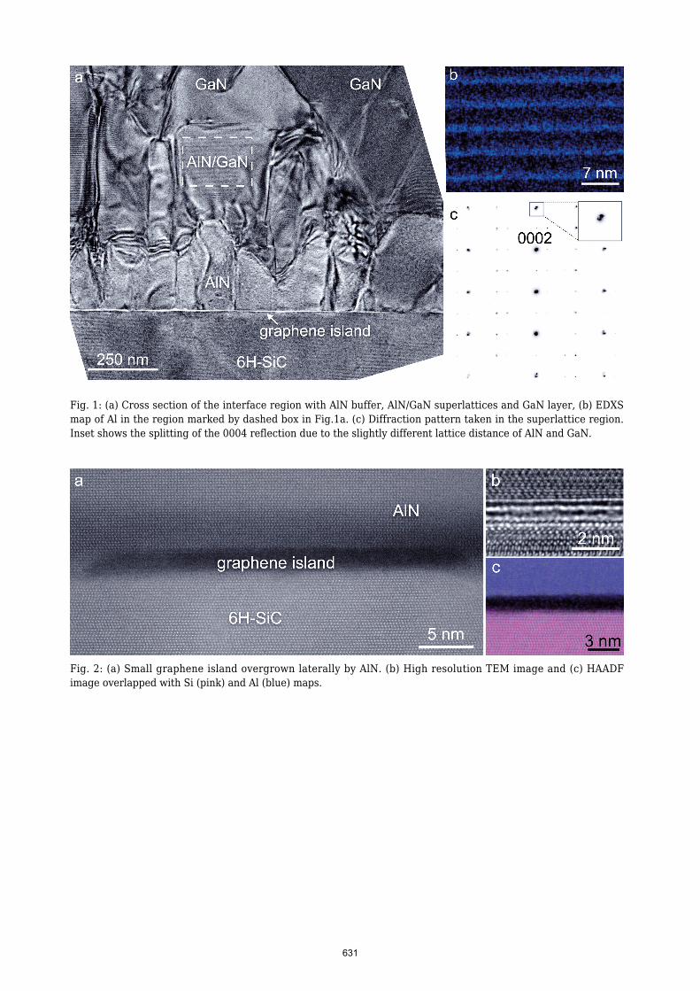
Fig. 1: (a) Cross section of the interface region with AlN buffer, AlN/GaN superlattices and GaN layer, (b) EDXSmap of Al in the region marked by dashed box in Fig.1a. (c) Diffraction pattern taken in the superlattice region.Inset shows the splitting of the 0004 reflection due to the slightly different lattice distance of AlN and GaN.
Fig. 2: (a) Small graphene island overgrown laterally by AlN. (b) High resolution TEM image and (c) HAADFimage overlapped with Si (pink) and Al (blue) maps.
631