
NI SMA-2164/2165 Test Fixture User Guide - National ... · PDF fileNI SMA-2164/2165 Test...
19
USER GUIDE NI SMA-2164/2165 Test Fixture Differential Digital I/O Accessory The NI SMA-2164/2165 test fixture is a breakout box for National Instruments differential digital waveform generator/analyzer modules, arbitrary waveform generators, and NI FlexRIO ™ adapter modules. This fixture provides an easy way to connect to other devices for testing and debugging. The NI SMA-2164 is intended for use with devices with a matching Infiniband connector such as NI 6561/6562 modules, NI 6583 adapter modules, and NI 6587 adapter modules. The NI SMA-2165 is intended for use with devices with matching VHDCI connectors such as NI 5421 modules and NI 6585 adapter modules. The NI SMA-2164/2165 may be compatible with other NI modules depending on the connector type and pinout. This guide explains how to set up and use the NI SMA-2164/2165 test fixture. Contents Conventions .............................................................................................................................. 2 What You Need to Get Started ................................................................................................. 3 Related Documentation ............................................................................................................ 3 Parts Locator ............................................................................................................................. 4 Installing Cables ....................................................................................................................... 6 Connecting Signals ................................................................................................................... 7 Using SMA Connectors .................................................................................................... 12 Making a Solder Connection ............................................................................................ 13 Terminating Signals .................................................................................................................. 15 Minimizing the Effects of Stubs ....................................................................................... 15 Differentially Terminating DIO and Control Signals ....................................................... 15 Using the Prototyping Area ...................................................................................................... 15 Prototyping Circuits.......................................................................................................... 16 Cleaning the Accessory ............................................................................................................ 16 Specifications............................................................................................................................ 17 Where to Go for Support .......................................................................................................... 18
Transcript of NI SMA-2164/2165 Test Fixture User Guide - National ... · PDF fileNI SMA-2164/2165 Test...

USER GUIDE
NI SMA-2164/2165 Test FixtureDifferential Digital I/O Accessory
The NI SMA-2164/2165 test fixture is a breakout box for National Instruments differential digital waveform generator/analyzer modules, arbitrary waveform generators, and NI FlexRIO™ adapter modules. This fixture provides an easy way to connect to other devices for testing and debugging.
The NI SMA-2164 is intended for use with devices with a matching Infiniband connector such as NI 6561/6562 modules, NI 6583 adapter modules, and NI 6587 adapter modules. The NI SMA-2165 is intended for use with devices with matching VHDCI connectors such as NI 5421 modules and NI 6585 adapter modules. The NI SMA-2164/2165 may be compatible with other NI modules depending on the connector type and pinout.
This guide explains how to set up and use the NI SMA-2164/2165 test fixture.
ContentsConventions .............................................................................................................................. 2What You Need to Get Started ................................................................................................. 3Related Documentation ............................................................................................................ 3Parts Locator............................................................................................................................. 4Installing Cables ....................................................................................................................... 6Connecting Signals ................................................................................................................... 7
Using SMA Connectors.................................................................................................... 12Making a Solder Connection ............................................................................................ 13
Terminating Signals.................................................................................................................. 15Minimizing the Effects of Stubs....................................................................................... 15Differentially Terminating DIO and Control Signals....................................................... 15
Using the Prototyping Area ...................................................................................................... 15Prototyping Circuits.......................................................................................................... 16
Cleaning the Accessory ............................................................................................................ 16Specifications............................................................................................................................ 17Where to Go for Support .......................................................................................................... 18
NI SMA-2164/2165 User Guide 2 ni.com
ConventionsThe following conventions are used in this manual:
<> Angle brackets that contain numbers separated by an ellipsis represent a range of values associated with a bit or signal name—for example, DIO <0..3>.
» The » symbol leads you through nested menu items and dialog box options to a final action. The sequence Options»Settings»General directs you to pull down the Options menu, select the Settings item, and select General from the last dialog box.
This icon denotes a note, which alerts you to important information.
This icon denotes a caution, which advises you of precautions to take to avoid injury, data loss, or a system crash. When this symbol is marked on a product, refer to the Specifications section for information about precautions to take.
bold Bold text denotes items that you must select or click in the software, such as menu items and dialog box options. Bold text also denotes parameter names.
italic Italic text denotes variables, emphasis, a cross-reference, or an introduction to a key concept. Italic text also denotes text that is a placeholder for a word or value that you must supply.
monospace Text in this font denotes text or characters that you should enter from the keyboard, sections of code, programming examples, and syntax examples. This font is also used for the proper names of disk drives, paths, directories, programs, subprograms, subroutines, device names, functions, operations, variables, filenames, and extensions.
© National Instruments Corporation 3 NI SMA-2164/2165 User Guide
What You Need to Get StartedTo set up and use the NI SMA-2164/2165, you need the following items:
❑ (NI SMA-2164 only) NI SHB12X-B12X LVDS cable assembly
❑ (NI SMA-2165 only) NI SHC68-C68-D3 cable assembly
❑ Compatible NI digital waveform generator/analyzer, NI FlexRIO adapter module, or other NI device installed in a PXI or CompactPCI chassis
You also may need the following optional items:
❑ SMA cables
❑ Resistors for termination or characterization. The NI SMA-2164/2165 ships populated with 0 Ω resistors.
❑ The documentation included with the digital waveform generator/analyzer and driver software
Related DocumentationRefer to the documentation set for the device that you are connecting to the NI SMA-2164/2165 for more information. Documentation is available at ni.com/manuals and in your hardware kit.
NI SMA-2164/2165 User Guide 4 ni.com
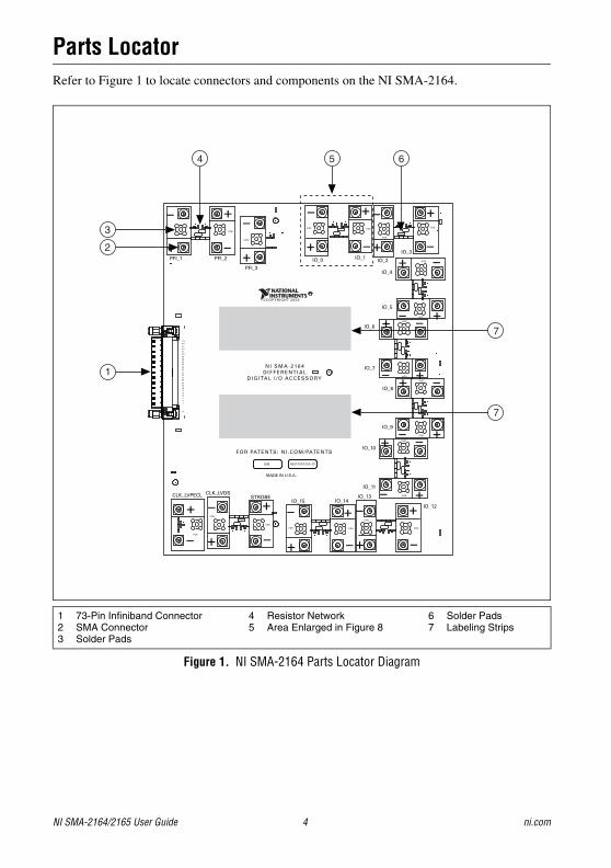
Parts LocatorRefer to Figure 1 to locate connectors and components on the NI SMA-2164.
Figure 1. NI SMA-2164 Parts Locator Diagram
1 73-Pin Infiniband Connector2 SMA Connector3 Solder Pads
4 Resistor Network5 Area Enlarged in Figure 8
6 Solder Pads7 Labeling Strips
1
2
STROBECLK_LVPECL
+
+
IO_3+
–
IO_7
IO_10
IO_14
IO_6
IO_11
IO_13
MADE IN U.S.A.
IO_15
ASSY192533A- 01
+
–
+
–
+
+
+
–
–
+–
–
–
–
IO_12
–
–
+
+
–+
IO_4
IO_5
IO_8
IO_2
IO_9
–
+
–+
+–
IO_1
+
–
–
+
+PFI_3
CLK_LVDS
+
PFI_2
+
–
+
–
PFI_1
VOS
VOS
VOS
VOS
VOS
VOS
VOS
VOS
VOS
VOS
VOS
IO_0
VOS
VOS
–
+
S/N
–VOS
VOS
–VOS
VOS
VOS
VOS
VOS
VOS
61
70
40
49
19
31
10
73
6467
5255
58
43
46
3437
2225
28
13
16
147
1
VOS
N I S M A - 2 16 4D I F F E R E NT I A L
D I G I TA L I / O AC C E S S O RY
FOR PATENTS: N I .COM/PATENTS
©COPYRIGHT 20 05
3
4 5 6
7
7
© National Instruments Corporation 5 NI SMA-2164/2165 User Guide
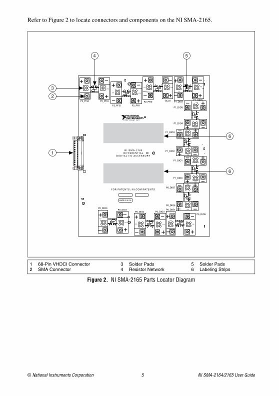
Refer to Figure 2 to locate connectors and components on the NI SMA-2165.
Figure 2. NI SMA-2165 Parts Locator Diagram
1 68-Pin VHDCI Connector2 SMA Connector
3 Solder Pads4 Resistor Network
5 Solder Pads6 Labeling Strips
1
2
–
+P2_PFI3
–
+
P2_PFI4
VOSVOS
–
+P2_PFI1
VOS
–P2_PFI2
+VOS
–
+GCLK
–
+VOS
P2_PFI0
VOS
P1_DIO6–
+ –
+P1_DIO7
VOS
VOS
–P0_DIO4
+
P0_DIO5+
–VOS
VOS
P0_DIO3P0_DIO2
–
+
+
–VOSVOS
–
+
+
–P1_DIO5
P1_DIO4
VOS
VOS
P0_DIO7
P0_DIO6
–
+
+
– VOS
VOS
–
–
+
+
P1_DIO1
P1_DIO0
VOS
VOS
3
4 5
6
P0_DIO1P0_DIO0
– +
–+VOS
VOS
P1_DIO2
P1_DIO3
MADE IN U.S.A.
–
+
+
– VOS
VOS
N I S M A - 2 16 5D I F F E R E NT I A L
D I G I TA L I / O AC C E S S O RY
FOR PATENTS: N I .COM/PATENTS
©COPYRIGHT 2011
6
NI SMA-2164/2165 User Guide 6 ni.com
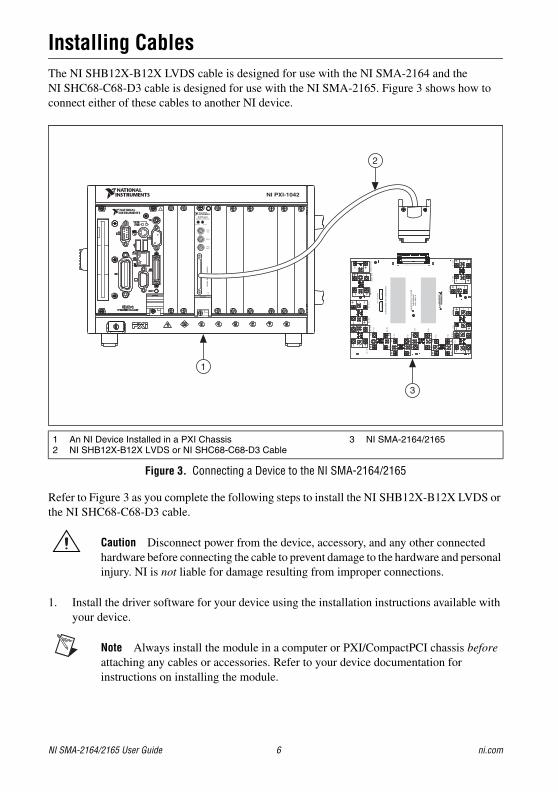
Installing CablesThe NI SHB12X-B12X LVDS cable is designed for use with the NI SMA-2164 and the NI SHC68-C68-D3 cable is designed for use with the NI SMA-2165. Figure 3 shows how to connect either of these cables to another NI device.
Figure 3. Connecting a Device to the NI SMA-2164/2165
Refer to Figure 3 as you complete the following steps to install the NI SHB12X-B12X LVDS or the NI SHC68-C68-D3 cable.
Caution Disconnect power from the device, accessory, and any other connected hardware before connecting the cable to prevent damage to the hardware and personal injury. NI is not liable for damage resulting from improper connections.
1. Install the driver software for your device using the installation instructions available with your device.
Note Always install the module in a computer or PXI/CompactPCI chassis before attaching any cables or accessories. Refer to your device documentation for instructions on installing the module.
1 An NI Device Installed in a PXI Chassis2 NI SHB12X-B12X LVDS or NI SHC68-C68-D3 Cable
3 NI SMA-2164/2165
NI PXI-6561100 MHz LVDS DIO
DIG
ITA
L D
ATA
& C
ON
TR
OL
PFI 0
ACCESS ACTIVE
CLKIN
CLKOUT
1
3
2
NI PXI-1042
ST
RO
BE
CLK
_LVP
EC
L
+
+ IO
_3
+ –IO
_7
I O_10
I O_14
IO
_6
I O_11
I O_13
MA
DE
IN U
.S.A
.I O_15
AS
SY
192
53
3A
-0
1
+–
+–+
++
–
–
+–
–
–
–
I O_12
–
–
+
+
–+ I
O_
4
IO
_5
IO
_8
IO
_2
I O_9
– +–+
+–
IO
_1
+ –
–+
+PF
I_
3
CLK
_LVD
S
+
PF
I_
2
+ –
+–
PF
I_
1
VO
S
VO
S
VO
S
VO
S
VO
S
VO
S
VO
S
VO
S
VO
S
VO
S
VO
S
IO
_0
VO
S
VO
S
– + S/
N
–VO
S
VO
S
–V
OS
VO
S
VO
S
VO
S
VO
S
VO
S
61
70
40
49
19
31
10 73
64
67
52
55 58
43
46
34
37
22
25
28
13
161 4 71
VO
S
NI S
MA
-2164D
IFFER
EN
TIA
LD
IGIT
AL I/O
AC
CE
SS
OR
Y
FOR
PA
TE
NT
S: N
I.CO
M/P
AT
EN
TS
©C
OP
YR
IGH
T 2005
© National Instruments Corporation 7 NI SMA-2164/2165 User Guide
2. Attach either end of the NI SHB12X-B12X LVDS or the NI SHC68-C68-D3 cable to the appropriate connector on your other NI device and secure the cable with the captive screws on the cable connector.
Notes Do not use cables other than the NI SHB12X-B12X LVDS cable with the NI SMA-2164, and do not use cables other than the NI SCH68-C68-D3 cable with the NI SMA-2165. NI is not liable for any damage resulting from improper cable connections.
3. Attach and secure the other end of the NI SHB12X-B12X LVDS or the NI SHC68-C68-D3 cable to the connector on the NI SMA-2164 or NI SMA-2165, respectively, and secure them together with the captive screws on the cable connector, as shown in Figure 3.
Connecting SignalsEach DIO, PFI, and clock channel on your connected NI device corresponds to a specific pin on the NI SMA-2164/2165. Most channels are routed differentially to high-bandwidth SMA connectors, but some channels may be used for other purposes depending on your NI device. Refer to you device documentation for more information.
You can make connections to the DIO, PFI, or clock channels on the NI SMA-2164/2165 using an SMA coaxial cable or by soldering directly to the inline circuits. Examples of how to make these connections are provided in the following sections.
Caution Before powering down the chassis, remove power from the prototyping area of the NI SMA-2164/2165. NI is not liable for any damage resulting from improper signal connections.
Caution Connections that exceed any of the maximum ratings for the NI SMA-2164/2165 or the connected NI device can damage the module and the computer. Maximum input ratings are provided in the Specifications section and in the specifications document that shipped with the other NI device. NI is not liable for any damage resulting from such signal connections.
NI SMA-2164/2165 User Guide 8 ni.com
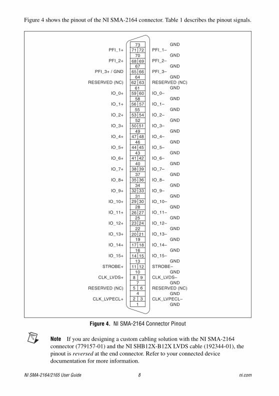
Figure 4 shows the pinout of the NI SMA-2164 connector. Table 1 describes the pinout signals.
Figure 4. NI SMA-2164 Connector Pinout
Note If you are designing a custom cabling solution with the NI SMA-2164 connector (779157-01) and the NI SHB12X-B12X LVDS cable (192344-01), the pinout is reversed at the end connector. Refer to your connected device documentation for more information.
GNDPFI_1–
GNDPFI_2–
GNDPFI_3–
GNDRESERVED (NC)
GNDIO_0–
GNDIO_1–
GNDIO_2–
GNDIO_3–
GNDIO_4–
GNDIO_5–
GNDIO_6–
GNDIO_7–
GNDIO_8–
GNDIO_9–
GNDIO_10–
GNDIO_11–
GNDIO_12–
GNDIO_13–
GNDIO_14–
GNDIO_15–
GNDSTROBE–
GNDCLK_LVDS–
GNDRESERVED (NC)
GNDCLK_LVPECL–
GND
PFI_1+
PFI_2+
PFI_3+ / GND
RESERVED (NC)
IO_0+
IO_1+
IO_2+
IO_3+
IO_4+
IO_5+
IO_6+
IO_7+
IO_8+
IO_9+
IO_10+
IO_11+
IO_12+
IO_13+
IO_14+
IO_15+
STROBE+
CLK_LVDS+
RESERVED (NC)
CLK_LVPECL+
7371 72
7068 69
6765 66
6462 63
6159 60
5856 57
5553 54
5250 51
4947 48
4644 45
4341 42
4038 39
3735 36
3432 33
3129 30
2826 27
2523 24
2220 21
1917 18
1614 15
1311 12
108 9
75 6
42 3
1
© National Instruments Corporation 9 NI SMA-2164/2165 User Guide
Refer to your device documentation for more information about the signals on your connected device. For information about how the signals on your connected device map to the SMA connectors on the NI SMA-2164/2165, visit ni.com/info and enter 216xpinmap.
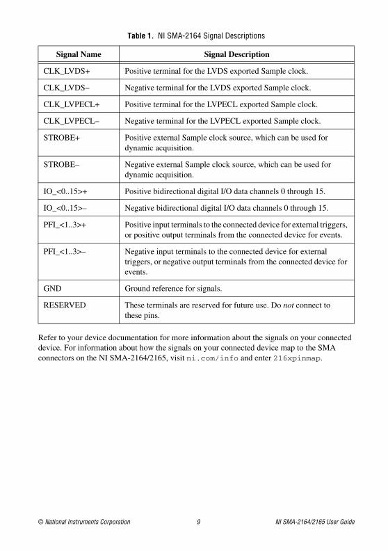
Table 1. NI SMA-2164 Signal Descriptions
Signal Name Signal Description
CLK_LVDS+ Positive terminal for the LVDS exported Sample clock.
CLK_LVDS– Negative terminal for the LVDS exported Sample clock.
CLK_LVPECL+ Positive terminal for the LVPECL exported Sample clock.
CLK_LVPECL– Negative terminal for the LVPECL exported Sample clock.
STROBE+ Positive external Sample clock source, which can be used for dynamic acquisition.
STROBE– Negative external Sample clock source, which can be used for dynamic acquisition.
IO_<0..15>+ Positive bidirectional digital I/O data channels 0 through 15.
IO_<0..15>– Negative bidirectional digital I/O data channels 0 through 15.
PFI_<1..3>+ Positive input terminals to the connected device for external triggers, or positive output terminals from the connected device for events.
PFI_<1..3>– Negative input terminals to the connected device for external triggers, or negative output terminals from the connected device for events.
GND Ground reference for signals.
RESERVED These terminals are reserved for future use. Do not connect to these pins.
NI SMA-2164/2165 User Guide 10 ni.com
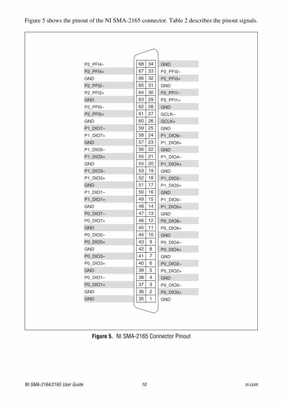
Figure 5 shows the pinout of the NI SMA-2165 connector. Table 2 describes the pinout signals.
Figure 5. NI SMA-2165 Connector Pinout
GND
GND
P0_DIO1+
P0_DIO1–
GND
P0_DIO3+
P0_DIO3–
GND
P0_DIO5+
P0_DIO5–
GND
P0_DIO7+
P0_DIO7–
GND
P1_DIO1+
P1_DIO1–
GND
P1_DIO3+
P1_DIO3–
GND
P1_DIO5+
P1_DIO5–
GND
P1_DIO7+
P1_DIO7–
GND
P2_PFI0+
P2_PFI0–
GND
P2_PFI2+
P2_PFI2–
GND
P2_PFI4+
P2_PFI4–
GND
P0_DIO0–
GND
P0_DIO2–
GND
P0_DIO4+
P0_DIO4–
P0_DIO0+
P0_DIO2+
GND
P0_DIO6+
P0_DIO6–
GND
P1_DIO0+
P1_DIO0–
GND
P1_DIO2+
P1_DIO2–
GND
P1_DIO4+
P1_DIO4–
GND
P1_DIO6+
P1_DIO6–
GND
GCLK+
GCLK–
GND
P2_PFI1+
P2_PFI1–
GND
P2_PFI3+
P2_PFI3–
GND68 34
67 33
66 32
65 31
64 30
63 29
62 28
61 27
60 26
59 25
58 24
57 23
56 22
55 21
54 20
53 19
52 18
51 17
50 16
49 15
48 14
47 13
46 12
45 11
44 10
43 9
42 8
41 7
40 6
39 5
38 4
37 3
36 2
35 1
© National Instruments Corporation 11 NI SMA-2164/2165 User Guide
Refer to your device documentation for more information about the signals on your connected device. For information about how the signals on your connected device map to the SMA connectors on the NI SMA-2164/2165, visit ni.com/info and enter 216xpinmap.
Table 2. NI SMA-2165 Signal Descriptions
Signal Name Signal Description
GLCK+ Positive terminal for the global clock.
GLCK– Negative terminal for the global clock.
P0_DIO<0..7>+ Positive bidirectional digital I/O data channels 0 through 7 on port 0.
P0_DIO<0..7>– Negative bidirectional digital I/O data channels 0 through 7 on port 0.
P1_DIO<0..7>+ Positive bidirectional digital I/O data channels 0 through 7 on port 1.
P1_DIO<0..7>– Negative bidirectional digital I/O data channels 0 through 7 on port 1.
P2_PFI<0..4>+ Positive input terminals to the connected device for external triggers, or positive output terminals from the connected device for events.
P2_PFI<0..4>– Negative input terminals to the connected device for external triggers, or negative output terminals from the connected device for events.
GND Ground reference for signals.
NI SMA-2164/2165 User Guide 12 ni.com
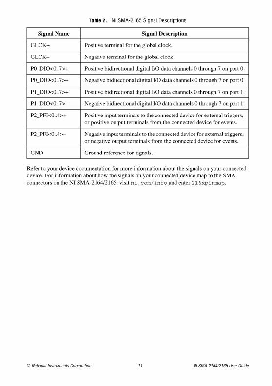
Using SMA ConnectorsEach signal pair is labeled on the NI SMA-2164/2165. These connectors are arranged so that you can make quick connections to each polarity using a standard SMA coaxial cable assembly. Connectivity is made by inserting the cable receptacle onto the appropriate connector and tightening the receptacle sufficiently.
Note Refer to the receptacle documentation to assure that proper connections are made to signal and ground.
Figure 6 shows how to make an SMA coaxial cable assembly connection.
Figure 6. SMA Coaxial Cable Connection
1 SMA Cable 2 SMA Connector
DIO
1
2
© National Instruments Corporation 13 NI SMA-2164/2165 User Guide
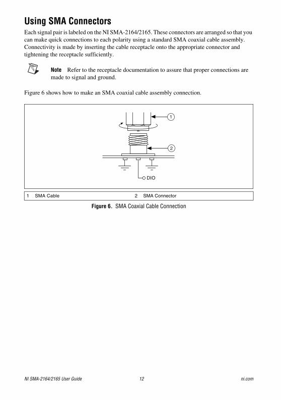
Making a Solder ConnectionEach signal pair is routed through a simple circuit to provide solder and probe access to the signals. Signal pairs are routed to a symmetric circuit, as shown in Figure 7.
Figure 7. Symmetric Circuit
SMA
SMASMA
0 Ω
0 Ω
R67
R84
R12
R11
R105
0 ΩR101
v
R63
R80
R377
R345
R4
R3
v
IO_1IO_0
SMA
SMA
SMA
0 Ω
0 Ω
0 ΩIO_1IO_0
R125 R129
R150 R142
NI SMA-2164/2165 User Guide 14 ni.com
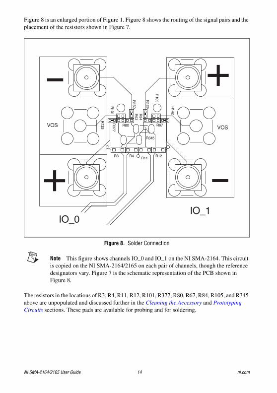
Figure 8 is an enlarged portion of Figure 1. Figure 8 shows the routing of the signal pairs and the placement of the resistors shown in Figure 7.
Figure 8. Solder Connection
Note This figure shows channels IO_0 and IO_1 on the NI SMA-2164. This circuit is copied on the NI SMA-2164/2165 on each pair of channels, though the reference designators vary. Figure 7 is the schematic representation of the PCB shown in Figure 8.
The resistors in the locations of R3, R4, R11, R12, R101, R377, R80, R67, R84, R105, and R345 above are unpopulated and discussed further in the Cleaning the Accessory and Prototyping Circuits sections. These pads are available for probing and for soldering.
IO_1IO_0
VOSVOS
+
+R
101 R84
R63
R105R
150
R129
R80 R67
R11
R345
R377
R125
R4R3 R12
R142
© National Instruments Corporation 15 NI SMA-2164/2165 User Guide
Terminating SignalsTermination of high-speed digital signals is necessary to prevent signal reflections and force signal channels to a known state when no signal is present. Pads for terminating resistors are connected to all DIO and control channels on the NI SMA-2164/2165. These pads are labeled in Figures 1 and 2 and are shown in more detail in Figure 8.
Note Proper termination needs are application-specific. For some special considerations for choosing resistor values, refer to the Cleaning the Accessory section.
Minimizing the Effects of StubsStubs are unterminated tributaries from the original signal path. Stubs decrease the signal quality of the system by adding reflections to the transmission channels. To minimize the effect of stubs, termination is placed at the end of the signal path.
Note Refer to your connected device documentation for more information about proper signal termination.
If your signal transmission line ends on the NI SMA-2164/2165, you can use the provided resistor pads to solder termination resistors. If your signal terminates somewhere other than the NI SMA-2164/2165, NI recommends terminating the transmission line at the final signal destination. Each signal pair is routed through a symmetric circuit, shown in Figure 7.
Differentially Terminating DIO and Control SignalsUnpopulated resistors like R80, R63, R67, and R84 in Figure 8 can be populated with 0402-sized resistors to provide termination. It is recommended that these resistors are each populated with 50 Ω resistors to provide the expected 100 Ω of differential termination.
Using the Prototyping AreaThe NI SMA-2164/2165 prototyping area is designed to aid you in the following tasks:
• Prototyping and testing circuits—Use the NI SMA-2164/2165 in conjunction with other NI devices for prototyping, evaluating, and testing custom circuits and/or components.
• Creating custom interfaces—Use the NI SMA-2164/2165 for creating custom interfaces to other cables or devices. You can use the prototyping area to mount and interface the integrated circuits (ICs) or connectors required for your application.
• Prototyping a DUT load board—Use the NI SMA-2164/2165 as a simple DUT interface board or as a prototype of a custom DUT load board.
The prototyping area is labeled in Figure 1. Also labeled in that diagram are the erasable labeling strips for your notes as you use the prototyping area.
NI SMA-2164/2165 User Guide 16 ni.com
Prototyping CircuitsEach signal pair is routed to a simple debug and prototyping circuitry illustrated in Figure 7.
By placing or removing components, each circuit can be configured to accomplish one of the following tasks, which are described in more detail in the following sections.
• Differentially terminate the signals—For more information about differential termination, refer to the Differentially Terminating DIO and Control Signals section.
• Externally provide a common mode or offset voltage to a differential signal—If an application requires an externally provided offset voltage, you may populate the R3, R4, R11, and R12 resistor locations with 0603-sized resistors to provide a connection point. For balanced application to a differential signal, it is recommended that R0 and R1 each be populated with a 3.74 kΩ resistor.
The node shared by the resistors in the R3, R4, R11, and R12 location is electrically connected between all DIO circuits.
• Externally probe or measure the common mode or offset of a differential signal—If an application requires that the offset voltage be measured on a differential signal, you can populate the R80 and R63 resistor locations. R80 and R63 are connected at a node which is connected to an SMA pad through a 0 Ω jumper. This SMA can be populated for coaxial connectivity to the offset voltage of the signal. The R80 and R63 resistor locations should each be 50 Ω if termination is required, else, larger values of 3.74 kΩ are more appropriate.
• Channel-to-channel connectivity—If it is required that two channels be connected to one another (for round-trip delay elimination for example), you can connect neighboring channels by populating a size 1206 0 jumper on resistor locations R345 and R377 in Figure 8. By populating these resistors, IO_0 connects to IO_1, IO_2 connects to IO_3, and so on, and CLKOUT_LVDS connects to STROBE.
Cleaning the AccessoryDisconnect all cables to the NI SMB-2164/2165 before cleaning. To remove light dust, use a soft, nonmetallic brush. To remove other contaminants, use alcohol wipes. The unit must be completely dry and free from contaminants before returning to service.
© National Instruments Corporation 17 NI SMA-2164/2165 User Guide
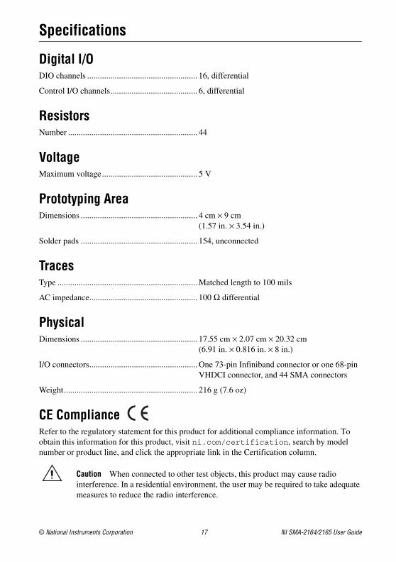
Specifications
Digital I/ODIO channels .................................................... 16, differential
Control I/O channels......................................... 6, differential
ResistorsNumber ............................................................. 44
VoltageMaximum voltage............................................. 5 V
Prototyping AreaDimensions ....................................................... 4 cm × 9 cm
(1.57 in. × 3.54 in.)
Solder pads ....................................................... 154, unconnected
TracesType .................................................................. Matched length to 100 mils
AC impedance................................................... 100 Ω differential
PhysicalDimensions ....................................................... 17.55 cm × 2.07 cm × 20.32 cm
(6.91 in. × 0.816 in. × 8 in.)
I/O connectors................................................... One 73-pin Infiniband connector or one 68-pin VHDCI connector, and 44 SMA connectors
Weight............................................................... 216 g (7.6 oz)
CE ComplianceRefer to the regulatory statement for this product for additional compliance information. To obtain this information for this product, visit ni.com/certification, search by model number or product line, and click the appropriate link in the Certification column.
Caution When connected to other test objects, this product may cause radio interference. In a residential environment, the user may be required to take adequate measures to reduce the radio interference.
NI SMA-2164/2165 User Guide 18 ni.com
Where to Go for SupportThe National Instruments Web site is your complete resource for technical support. At ni.com/support you have access to everything from troubleshooting and application development self-help resources to email and phone assistance from NI Application Engineers.
A Declaration of Conformity (DoC) is our claim of compliance with the Council of the European Communities using the manufacturer’s declaration of conformity. This system affords the user protection for electromagnetic compatibility (EMC) and product safety. You can obtain the DoC for your product by visiting ni.com/certification. If your product supports calibration, you can obtain the calibration certificate for your product at ni.com/calibration.
National Instruments corporate headquarters is located at 11500 North Mopac Expressway, Austin, Texas, 78759-3504. National Instruments also has offices located around the world to help address your support needs. For telephone support in the United States, create your service request at ni.com/support and follow the calling instructions or dial 512 795 8248. For telephone support outside the United States, visit the Worldwide Offices section of ni.com/niglobal to access the branch office Web sites, which provide up-to-date contact information, support phone numbers, email addresses, and current events.

© 2005–2011 National Instruments Corporation. All rights reserved.
374063B-01 Oct11
LabVIEW, National Instruments, NI, ni.com, the National Instruments corporate logo, and the Eagle logo are trademarks of National Instruments Corporation. Refer to the Trademark Information at ni.com/trademarks for other National Instruments trademarks. Other product and company names mentioned herein are trademarks or trade names of their respective companies. For patents covering National Instruments products/technology, refer to the appropriate location: Help»Patents in your software, the patents.txt file on your media, or the National Instruments Patents Notice at ni.com/patents. Refer to the Export Compliance Information at ni.com/legal/export-compliance for the National Instruments global trade compliance policy and how to obtain relevant HTS codes, ECCNs, and other import/export data.