New slant on photonic crystal fibers - Swinburne...New slant on photonic crystal fibers Hong C....
12
New slant on photonic crystal fibers Hong C. Nguyen, Peter Domachuk and Benjamin J. Eggleton Centre for Ultrahigh-bandwidth Devices for Optical Systems (CUDOS), School of Physics, University of Sydney, NSW 2006 Australia [email protected] Michael J. Steel RSoft Design Group, Inc., and Centre for Ultrahigh-bandwidth Devices for Optical Systems (CUDOS), 304/56 Mallett St, Camperdown, NSW 2050 Australia Martin Straub and Min Gu Centre for Micro-Photonics and Centre for Ultrahigh-bandwidth Devices for Optical Systems (CUDOS), Swinburne University of Technology, Hawthorn, Victoria 3122 Australia Mikhail Sumetsky OFS Laboratories, 700 Mountain Ave, Murray Hill NJ 07974 USA Abstract: We present the novel use of microstructured optical fibers not as “light-pipes”, but in a transverse geometry to manipulate the light propagating across the fiber. Fundamental and higher-order bandgaps were observed experimentally in this geometry using a number of techniques. The comparison of the measured spectra with photonic band structure and Finite-Difference Time-Domain simulations provide strong evidence that the spectral features are a result of the periodic nature of the fiber microstructure in the transverse direction. ©2004 Optical Society of America OCIS codes: (050.0050) Diffraction and gratings; (060.2340) Fiber optics components Reference and links 1. S. John, "Strong Localization of Photons in Certain Disordered Dielectric Superlattices," Phys. Rev. Lett. 58, 2486-2489 (1987). 2. E. Yablonovitch, "Inhibited Spontaneous Emission in Solid-State Physics and Electronics," Phys. Rev. Lett. 58, 2059-2062 (1987). 3. J.D. Joannopoulos, R.D. Meade, and J.N. Winn, Photonic Crystals: Molding the Flow of Light. (Princeton University Press, 1995). 4. S.Y. Lin, J.G. Fleming, D.L. Hetherington, B.K. Smith, R. Biswas, K.M. Ho, M.M. Sigalas, W. Zubrzycki, S.R. Kurtz, and J. Bur, "A three-dimensional photonic crystal operating at infrared wavelengths," Nature 394, 251-253 (1998). 5. A. Mekis, J.C. Chen, I. Kurland, S.H. Fan, P.R. Villeneuve, and J.D. Joannopoulos, "High transmission through sharp bends in photonic crystal waveguides," Phys. Rev. Lett. 77, 3787-3790 (1996). 6. P.V. Braun and P. Wiltzius, "Microporous materials - Electrochemically grown photonic crystals," Nature 402, 603-604 (1999). 7. S.Y. Lin, J.G. Fleming, and E. Chow, "Two- and three-dimensional photonic crystals built with VLSI tools," MRS Bull. 26, 627-631 (2001). 8. O. Toader and S. John, "Square spiral photonic crystals: Robust architecture for microfabrication of materials with large three-dimensional photonic band gaps," Phys. Rev. E 66, (2002). 9. V.L. Colvin, "From opals to optics: Colloidal photonic crystals," MRS Bull. 26, 637-641 (2001). 10. M. Straub and M. Gu, "Near-infrared photonic crystals with higher-order bandgaps generated by two- photon photopolymerization," Opt. Lett. 27, 1824-1826 (2002). 11. M. Campbell, D.N. Sharp, M.T. Harrison, R.G. Denning, and A.J. Turberfield, "Fabrication of photonic crystals for the visible spectrum by holographic lithography," Nature 404, 53-56 (2000). 12. S. Shoji and S. Kawata, "Photofabrication of three-dimensional photonic crystals by multibeam laser interference into a photopolymerizable resin," Appl. Phys. Lett. 76, 2668-2670 (2000). (C) 2004 OSA 19 April 2004 / Vol. 12, No. 8 / OPTICS EXPRESS 1528 #3665 - $15.00 US Received 15 January 2004; revised 21 February 2004; accepted 26 February 2004
Transcript of New slant on photonic crystal fibers - Swinburne...New slant on photonic crystal fibers Hong C....
New slant on photonic crystal fibers Hong C. Nguyen, Peter Domachuk and Benjamin J. Eggleton
Centre for Ultrahigh-bandwidth Devices for Optical Systems (CUDOS), School of Physics, University of Sydney,
NSW 2006 Australia [email protected]
Michael J. Steel
RSoft Design Group, Inc., and Centre for Ultrahigh-bandwidth Devices for Optical Systems (CUDOS), 304/56 Mallett St, Camperdown, NSW 2050 Australia
Martin Straub and Min Gu
Centre for Micro-Photonics and Centre for Ultrahigh-bandwidth Devices for Optical Systems (CUDOS), Swinburne University of Technology, Hawthorn, Victoria 3122 Australia
Mikhail Sumetsky
OFS Laboratories, 700 Mountain Ave, Murray Hill NJ 07974 USA
Abstract: We present the novel use of microstructured optical fibers not as “light-pipes”, but in a transverse geometry to manipulate the light propagating across the fiber. Fundamental and higher-order bandgaps were observed experimentally in this geometry using a number of techniques. The comparison of the measured spectra with photonic band structure and Finite-Difference Time-Domain simulations provide strong evidence that the spectral features are a result of the periodic nature of the fiber microstructure in the transverse direction. ©2004 Optical Society of America OCIS codes: (050.0050) Diffraction and gratings; (060.2340) Fiber optics components
Reference and links 1. S. John, "Strong Localization of Photons in Certain Disordered Dielectric Superlattices," Phys. Rev. Lett.
58, 2486-2489 (1987). 2. E. Yablonovitch, "Inhibited Spontaneous Emission in Solid-State Physics and Electronics," Phys. Rev. Lett.
58, 2059-2062 (1987). 3. J.D. Joannopoulos, R.D. Meade, and J.N. Winn, Photonic Crystals: Molding the Flow of Light. (Princeton
University Press, 1995). 4. S.Y. Lin, J.G. Fleming, D.L. Hetherington, B.K. Smith, R. Biswas, K.M. Ho, M.M. Sigalas, W. Zubrzycki,
S.R. Kurtz, and J. Bur, "A three-dimensional photonic crystal operating at infrared wavelengths," Nature 394, 251-253 (1998).
5. A. Mekis, J.C. Chen, I. Kurland, S.H. Fan, P.R. Villeneuve, and J.D. Joannopoulos, "High transmission through sharp bends in photonic crystal waveguides," Phys. Rev. Lett. 77, 3787-3790 (1996).
6. P.V. Braun and P. Wiltzius, "Microporous materials - Electrochemically grown photonic crystals," Nature 402, 603-604 (1999).
7. S.Y. Lin, J.G. Fleming, and E. Chow, "Two- and three-dimensional photonic crystals built with VLSI tools," MRS Bull. 26, 627-631 (2001).
8. O. Toader and S. John, "Square spiral photonic crystals: Robust architecture for microfabrication of materials with large three-dimensional photonic band gaps," Phys. Rev. E 66, (2002).
9. V.L. Colvin, "From opals to optics: Colloidal photonic crystals," MRS Bull. 26, 637-641 (2001). 10. M. Straub and M. Gu, "Near-infrared photonic crystals with higher-order bandgaps generated by two-
photon photopolymerization," Opt. Lett. 27, 1824-1826 (2002). 11. M. Campbell, D.N. Sharp, M.T. Harrison, R.G. Denning, and A.J. Turberfield, "Fabrication of photonic
crystals for the visible spectrum by holographic lithography," Nature 404, 53-56 (2000). 12. S. Shoji and S. Kawata, "Photofabrication of three-dimensional photonic crystals by multibeam laser
interference into a photopolymerizable resin," Appl. Phys. Lett. 76, 2668-2670 (2000).
(C) 2004 OSA 19 April 2004 / Vol. 12, No. 8 / OPTICS EXPRESS 1528#3665 - $15.00 US Received 15 January 2004; revised 21 February 2004; accepted 26 February 2004
13. A. Rosenberg, R.J. Tonucci, H.B. Lin, and E.L. Shirley, "Photonic-band-structure effects for low-index-contrast two-dimensional lattices in the near-infrared," Phys. Rev. B 54, R5195-R5198 (1996).
14. A. Rosenberg, R.J. Tonucci, H.B. Lin, and A.J. Campillo, "Near-infrared two-dimensional photonic band-gap materials," Opt. Lett. 21, 830-832 (1996).
15. P. Russell, "Photonic crystal fibers," Science 299, 358-362 (2003). 16. T.A. Birks, J.C. Knight, and P.S. Russell, "Endlessly single-mode photonic crystal fiber," Opt. Lett. 22,
961-963 (1997). 17. J.C. Knight, T.A. Birks, R.F. Cregan, P.S. Russell, and J.P. de Sandro, "Large mode area photonic crystal
fibre," Electron. Lett. 34, 1347-1348 (1998). 18. J.C. Knight, J. Arriaga, T.A. Birks, A. Ortigosa-Blanch, W.J. Wadsworth, and P.S. Russell, "Anomalous
dispersion in photonic crystal fiber," IEEE Photonics Technol. Lett. 12, 807-809 (2000). 19. N.G.R. Broderick, T.M. Monro, P.T. Bennett, and D.T. Richardson, "Nonlinearity in holey optical fibers:
measurement and future opportunities," Opt. Lett. (USA) vol.24, no.20, 1395-1397 (1999). 20. P. Mach, M. Dolinski, K.W. Baldwin, J.A. Rogers, C. Kerbage, R.S. Windeler, and B.J. Eggleton, "Tunable
microfluidic optical fiber," Appl. Phys. Lett. 80, 4294-4296 (2002). 21. J.C. Knight, J. Broeng, T.A. Birks, and P.S.J. Russel, "Photonic band gap guidance in optical fibers,"
Science 282, 1476-1478 (1998). 22. R.F. Cregan, B.J. Mangan, J.C. Knight, T.A. Birks, P.S. Russell, P.J. Roberts, and D.C. Allan, "Single-
mode photonic band gap guidance of light in air," Science 285, 1537-1539 (1999). 23. J.C. Knight, T.A. Birks, P.S.J. Russell, and J.G. Rarity, "Bragg scattering from an obliquely illuminated
photonic crystal fiber," Appl. Optics 37, 449-452 (1998). 24. H.C. Nguyen, P. Domachuk, M. Sumetsky, M.J. Steel, M. Straub, M. Gu, and B.J. Eggleton. "Lateral
thinking with photonic crystal fibers" in Postdeadline paper at IEEE Lasers and Electro-Optics Society Meeting (Tucson, Arizona, 2003), pp.
25. BandSOLVETM 1.2.0.(RSoft Design Group, Inc.), 2003 26. K. Sakoda, "Symmetry, Degeneracy, and Uncoupled Modes in 2-Dimensional Photonic Lattices," Phys.
Rev. B 52, 7982-7986 (1995). 27. S. Rowson, A. Chelnokov, C. Cuisin, and J.M. Lourtioz, "Two-dimensional photonic bandgap reflectors for
free-propagating beams in the mid-infrared," J. Opt. A-Pure Appl. Opt. 1, 483-489 (1999). 28. FullWAVETM 3.0.1.(RSoft Design Group, Inc.), 2003 29. J.C. Knight, T.A. Birks, P.S. Russell, and D.M. Atkin, "All-silica single-mode optical fiber with photonic
crystal cladding," Opt. Lett. 21, 1547-1549 (1996). 30. A. Argyros, I.M. Bassett, M.A. van Eijkelenborg, M.C.J. Large, J. Zagari, N.A.P. Nicorovici, R.C.
McPhedran, and C.M. de Sterke, "Ring structures in microstructured polymer optical fibres," Opt. Express 9, 813-820 (2001), http://www.opticsexpress.org/abstract.cfm?URI=OPEX-9-13-813.
31. F. Ladouceur, "Roughness, inhomogeneity, and integrated optics," J. Lightwave Technol. 15, 1020-1025 (1997).
32. P. Domachuk, H.C. Nguyen, B.J. Eggleton, M. Straub, M. Gu, "Microfluidic Tunable Tall MicroChip", App. Phys. Lett. in press, March 2004
1. Introduction
One dimensional (1D) periodic structures have long been known to reflect incident light strongly for certain frequency ranges and polarizations. The extension of this 1D phenomenon to two- and three-dimensional (2D & 3D) photonic crystals (PC) [1, 2] has since generated enormous interest in photonics. The most attention has been paid to the generation of Photonic Bandgaps (PBGs) in multi-dimensional PCs which prohibit the propagation of light through the structure [3] like the 1D periodic structures, but for a range of directions. PBG materials have been studied extensively as a method of controlling light in photonic devices, and to confine photons inside structural defects, thereby achieving wave-guiding inside PC microchannels by confining lateral propagation [4, 5].
Studies of PCs and their applications have been performed predominantly in semiconductors [6-9], photosensitive polymers [10-12] and nanochannel glasses [13, 14]. Recently they have also been incorporated into optical fibers, through the introduction of Photonic Crystal Fibers (PCFs) [15]. Unlike conventional fibers, PCFs have an array of holes along their length that act as the cladding, which is responsible for their unusual optical properties. In particular, these fibers can exhibit single-mode operation over a broad range of wavelengths [16] and large mode areas [17], as well as unique dispersion and nonlinear characteristics [18, 19], leading to a range of new applications [15]. PCFs also offer opportunities for a new class of tunable optical filters and sensors based on microfluidic principles, taking advantage of the air-holes [20].
(C) 2004 OSA 19 April 2004 / Vol. 12, No. 8 / OPTICS EXPRESS 1529#3665 - $15.00 US Received 15 January 2004; revised 21 February 2004; accepted 26 February 2004
Of particular interest are PCFs with a periodic arrangement of holes surrounding a core, that can guide light by PBG effects [21]. These fibers are essentially 2D PCs in the transverse geometry that extend longitudinally along the length of the fiber. The fiber core behaves as a point-defect, through which light is guided not necessarily by total internal reflection, but instead by the PBG effect. Such guidance by the PBG effect has been experimentally demonstrated, with the guidance of light in a PCF consisting of an air-core surrounded by a hexagonal hole structure [22].
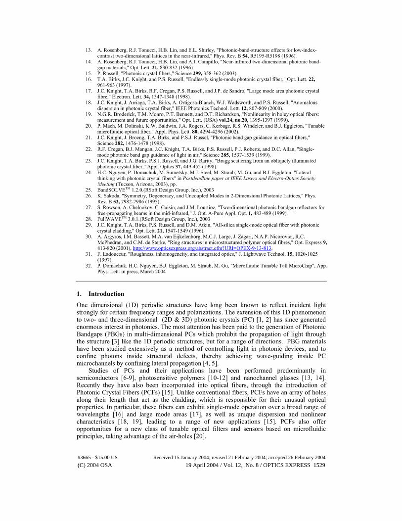
In this paper, we introduce another application of PCFs: the manipulation of light propagating transversely across the fibre. Figure 1 illustrates such a geometry, where light enters the PCF from the side and interacts with the periodic microstructure. The light then emerges at a series of angles forming diffraction spots, each differing spectrally [23, 24].
This transverse PCF geometry offers a new context for these fibers in the field of microphotonics, where the cross-sectional microstructure would resemble the layout of a device with the required functionalities. Using PCFs in this context offers new opportunities for optical devices and at the same time raises a new set of challenges in optical fiber design and fabrication.
Κ
28 µm
Μ Γ
125 µm
Fig. 1. Schematic of the PCF in the transverse geometry, where the light propagates across the fiber. Inset shows an SEM micrograph of the PCF microstructure.
In this paper we present an experimental characterization of a PCF in this transverse geometry. We use a combination of Fourier Transform Infrared (FTIR) spectroscopy and a diffraction-grating based Optical Spectrum Analyzer (OSA) to characterize the spectral response of the fiber in the 0.8 – 4 µm wavelength range. These results are compared with theoretical analyses of the band structure and the spectral response of the finite system. These preliminary experimental results highlight the new device concepts offered by PCFs and address some of the photonic crystal fabrication issues encountered in other techniques such as lithography.
This paper is structured as follows. In Section 2, we describe the PCF and the experimental methods used to spectrally characterize the fiber. Section 3 covers the theoretical analyses and predictions. In Section 4 we present and compare the experimental results with the theoretical analyses. Finally in Section 5, we conclude with a discussion of future work.
2. Experimental methods
2.1 Fiber structure
Figure 1 shows a cross-sectional schematic and a magnified Scanning Electron Microscope (SEM) image of the PCF, fabricated by Crystal Fibers A/S (Denmark). It is a silica fiber with a diameter of 125 µm and a refractive index of 1.44. Embedded within is a PC microstructure that consists of a regular, hexagonal array of holes, giving the structure a refractive index contrast of ∆n=0.44. The holes have an overall average diameter and spacing of 0.78 µm and 1.39 µm respectively. The structure also consists of a central defect, where a hole is replaced by a solid core. The crystallographic axes Γ-M and Γ-K are also shown in the figure. In this
(C) 2004 OSA 19 April 2004 / Vol. 12, No. 8 / OPTICS EXPRESS 1530#3665 - $15.00 US Received 15 January 2004; revised 21 February 2004; accepted 26 February 2004
paper, only the characterization along the Γ-M is presented as the large diameter air holes at the vertex of the hexagon detract from the observation of photonic band-gap effects along the Γ-K axis.
Note from Fig. 1 that the diameter of the holes and their spacing vary significantly throughout the fiber, especially in the outer few rings. In the past, this has been regarded as being of minor significance as the focus has been on the longitudinal propagation of light along the fiber axis, which is largely dependent upon the inner few rings surrounding the light-guiding core. In this geometry, however, all holes play equally important roles. This will be discussed further below. 2.2 FTIR spectroscopy
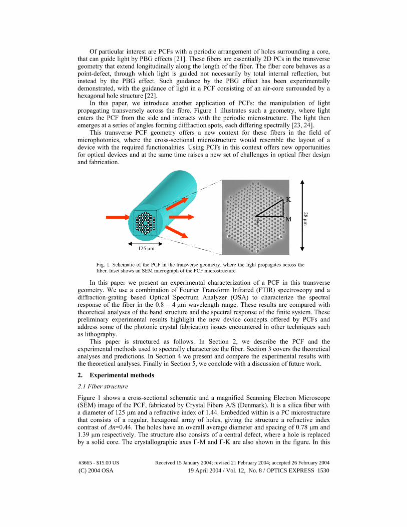
For the spectral characterization in the 1.4 – 4 µm range, a Nicolet NEXUS FTIR spectrometer attached to a Nicolet CONTINUUM Infrared microscope was used. Both transmission and reflection spectra were measured. The spectrometer was equipped with a Glowbar source and an XT-KBr beam splitter, while the microscope was equipped with 32x, 0.65 numerical aperture Reflechromat objective and condenser lenses, a ZnSe Infrared polarizer and a MCT detector. The lenses were mirror-based such that the half-angle of the incident beam had a range of 18 - 41°, with a weighted average of roughly 30°, while the fraction of the beam with a half-angle less than 18° was blocked out (Figure 2a). The reference to the illumination of the fiber along a crystallographic axis therefore becomes ambiguous. The incident beam undergoes refraction at the outer surface of the PCF, which we approximate to be flat. By applying Snell’s Law, the angular range inside the cladding then becomes 12 - 27°, with the average of roughly 20°.
Objective Lens
Source
Polarizer
Rotatable Fiber Mount
Transverse Fiber
Fiber Chuck
Launch Fiber
Detector Fiber
OSA
10x Objective Lens
CCDCamera
(c) (d)
Launch fiber
Detector fiber
PCF
(a)
Condenser
Focal plane for reflection measurement
Focal plane for transmission measurement
Γ-MStacking
(b)
Fig. 2. A schematic of the FTIR setup (a) and the focal plane used in the reflection and transmission measurements (b). A schematic of the OSA setup (c) and the image through the CCD camera (d) is also shown.
(C) 2004 OSA 19 April 2004 / Vol. 12, No. 8 / OPTICS EXPRESS 1531#3665 - $15.00 US Received 15 January 2004; revised 21 February 2004; accepted 26 February 2004

In the case of the transmission spectra, both the objective and the condenser were focused to the centre of the PC structure. The spectra were measured for unpolarized and two orthogonally polarized light beams (defined in Section 3), using a polarizer that was known to function effectively above 2 µm. Each spectrum was averaged over 200 scans, measured at 4 cm-1 resolution with the same aperture size, and was referenced against a free-space spectrum with the appropriate polarizer in place. For the reflectance, 1000-scan spectra were recorded at 2 cm-1 resolution for the same aperture size and polarizations, but referenced against the reflectance spectrum of a microscope cover slip surface. Here, the incident beam was focused onto the top of the PC structure for the PCF as shown in Fig. 2b.
2.3 OSA
In the 0.8 – 1.7 µm range, only transmission spectra were measured. Here, an ANDO white-light source and an Agilent 86140B Optical Spectrum Analyzer (OSA) were used. Two lengths of Single Mode Fibres (SMFs, equivalent to Corning SMF-28 fibers), denoted as the launch and detector fibers, were coupled to the source and OSA to illuminate the PCF and collect the transmitted light (Figure 2c). These fibers have a quoted numerical aperture of 0.13, and were measured to be single-moded above 1.15 µm.
For the alignment, first the launch and detector fibers were positioned coaxially with approximately 130 µm of longitudinal separation. The 125 µm diameter PCF was then inserted in-between. An imaging system, comprising of a 10x objective and a CCD camera, was setup to observe the fiber alignments in place (Fig. 2d). The PCF was then visually aligned vertically and rotationally, such that the Γ-M axis coincided with the launch fiber axis.
Spectra were then measured using the OSA, with the settings: 10 nm bandwidth resolution; -70 dBm sensitivity; and average over 20 scans. This was performed for two orthogonal polarizations (defined in Section 3), using a polarizer that was know to work effectively above 1.2 µm.
3. Theory
Two theoretical tools were used to obtain insight into the experimental characterization of the PCF. Photonic band structure, which predicts the properties of infinitely periodic systems, was used to predict the position of PBGs for an idealized PCF structure consisting of uniform hole sizes. On the other hand, Finite-Difference Time-Domain (FDTD) simulations were used to perform spectral analyses of the finite system.
Both these analyses were performed in 2D. In doing so, we neglect the divergence of the input beam and diffracted beams, after interacting with the structure, into the third dimension normal to the transverse geometry. In both the FTIR and the OSA setup, the source and the detector are separated by several Rayleigh ranges or more, with the implication that the 2D approximation is not entirely valid. We use this approximation however, as full 3D simulations require overwhelmingly intensive computation. Nevertheless, the agreement of our theoretical and experimental results validates our use of 2D modeling as an initial investigation.
3.1 Band structure
Due to the comparatively low refractive index contrast of the PCF, a complete PBG is not expected for this structure. We analyze its band structure regardless, as it may contain partial PBGs. An initial estimate of the bandgap positions is obtained from band structure calculations. For this, we use a commercial implementation of the plane wave expansion method [25]. In this paper, we concentrate on one of the two major symmetry axes of the hexagonal structure, Γ-M, which is shown in Figure 1.
(C) 2004 OSA 19 April 2004 / Vol. 12, No. 8 / OPTICS EXPRESS 1532#3665 - $15.00 US Received 15 January 2004; revised 21 February 2004; accepted 26 February 2004
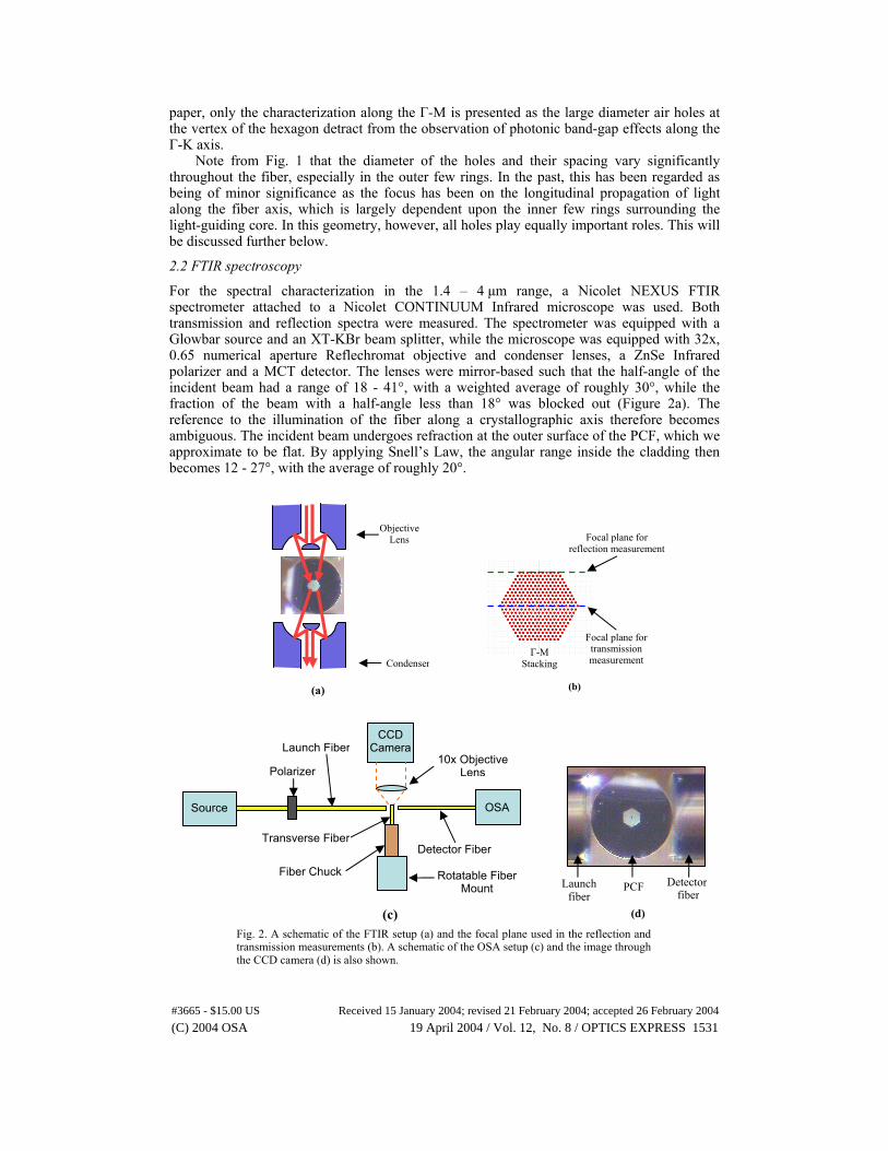
Fig. 3 shows the corresponding band diagram along the Γ-M axis, for TM and TE polarizations. These are defined as follows: for light propagating across the PCF, the electric field oriented parallel and perpendicular to the cylinders is considered TM and TE respectively. Each band corresponds to a mode, for which the spatial parity in the in-plane direction normal to Γ-M (i.e., parallel to M-K axis. See Fig. 1) may be either odd or even [26].
The solid and dashed lines in Fig. 3 indicate bands with even and odd parity respectively. The shaded rectangles that span horizontally across the band diagrams indicate partial photonic bandgaps.
Band structures for OSA measurements
The incident beam in the OSA setup has a half-angle range of only 0 – 7.5°, across which the intensity distribution is Gaussian centered around 0°. We therefore make an approximation that the PCF microstructure is illuminated by plane waves at normal incidence. Due to the even spatial parity of plane waves, they will only couple into even-parity modes inside the microstructure [26]. The odd-parity modes are not excited, and are therefore neglected. As a result, extra partial bandgaps appear at normalized frequencies above 1 (Fig. 3).
In the FTIR setup however, the angular range of the incident beam is much larger, and the angular intensity distribution is not Gaussian. Hence we cannot neglect certain modes due to their spatial parity. Furthermore, no part of the beam is incident along the Γ-M axis, but rather from the quoted angular range, in both the off-axis and out-of-plane dimensions (Fig. 4(a), left). Thus the band structure in Fig. 3 does not relate very well to the FTIR measurements.
We deal with this by the following: In the off-axis case, for a given incidence angle α, the incident wave has a transverse component related to the angular frequency by k⊥ = (ω/c) sin (α). The band structure for each incident angle is calculated along a path parallel to the Γ-M axis, but displaced along the M-K axis by k⊥ . This is indicated by the line AB in Fig. 4(a) (right). Since k⊥ increases with frequency, this is equivalent to taking the intersection between the 2D bands and a plane at an angle α with the ω axis [27]. By using this method, we are not required to explicitly calculate the propagation direction of the waves inside the microstructure. The out-of-plane band structures are obtained in an equivalent manner, but with k⊥ varying in the out-of-plane dimension. This is described in more detail in [27].
Figure 4(b) shows the band structures calculated for 20° incidence in the off-axis and out-of-plane dimensions. Only one “hybrid polarization” for the out-of-plane band structure is calculated, since TE and TM polarizations cannot be distinguished in this dimension. The dark, horizontal shade indicate the partial bandgap predicted for this incident angle. We also take into account the angular range of the incident wave, by assuming that the predicted bandgaps for each incident angle will contribute to the transmission and reflection spectra. Further, we
Fig. 3. Band structure along Γ-M axis, for TM (left) and TE (right) polarizations. Solid and dashed lines indicate bands corresponding to modes with even and odd spatial parity, respectively. The horizontal, rectangular shades indicate partial photonic bandgaps.
TM polarization TE polarization
(C) 2004 OSA 19 April 2004 / Vol. 12, No. 8 / OPTICS EXPRESS 1533#3665 - $15.00 US Received 15 January 2004; revised 21 February 2004; accepted 26 February 2004

approximate the intensity distribution to be uniform across this range. The lighter horizontal shades in Fig. 4b indicate the superposition of the partial bandgaps predicted for each incident angle. As expected, the lighter shades are wider than the corresponding darker shades, implying that the measured bandgaps should be widened due to the large angular range of the incident beam.
The band structures calculated for OSA and FTIR measurements both indicate that the fundamental bandgap is wider in the TE polarization, while the opposite is true for the 2nd-
order bandgap. This is compared with experimental results in Section 4.
Off-axis incidence
3.3 FDTD
A more complete description of the system was obtained through FDTD simulations [28]. Figure 5 illustrates the basic simulation geometry in the OSA measurements, with the transverse PCF and the launch and detector SMFs above and below. The core of the two SMFs and the cladding of all three fibers, were assigned a refractive index of 1.445 and 1.440 respectively. All other regions, including the holes of the PCF, were assigned an index of 1. The incident beam was launched within the bottom SMF, with a beam width of 10.4 µm corresponding to the fundamental mode supported by the fibre at the average wavelength of
Fig. 4. (a) illustrates off-axis and out-of-plane incidence (left); and the path AB along which band structure is calculated for off-axis incidence (right). Band diagrams for 20° incidence in the off-axis and out-of-plane dimensions are shown in (b). Dark, horizontal shades indicate bandgaps predicted for this incident angle. The lighter, wider shades indicate the superposition of the bandgaps predicted for each incident angle in the range 12 – 27 °.
(a)
Band structures for FTIR measurements
Off-axis: TM polarization
Off-axis:TE polarization
Out-of-plane: Hybrid polarization
(b)
α M KB
Out-of-plane incidence A
Γ k⊥
(C) 2004 OSA 19 April 2004 / Vol. 12, No. 8 / OPTICS EXPRESS 1534#3665 - $15.00 US Received 15 January 2004; revised 21 February 2004; accepted 26 February 2004
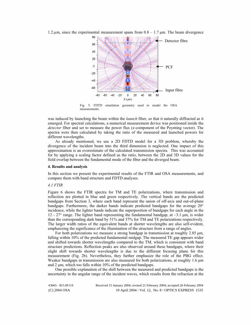
1.2 µm, since the experimental measurement spans from 0.8 – 1.7 µm. The beam divergence
was induced by launching the beam within the launch fiber, so that it naturally diffracted as it emerged. For spectral calculations, a numerical measurement device was positioned inside the detector fiber and set to measure the power flux (z-component of the Poynting vector). The spectra were then calculated by taking the ratio of the measured and launched powers for different wavelengths.
Detector f
As already mentioned, we use a 2D FDTD model for a 3D problem, whereby the divergence of the incident beam into the third dimension is neglected. One impact of this approximation is an overestimate of the calculated transmission spectra. This was accounted for by applying a scaling factor defined as the ratio, between the 2D and 3D values for the field overlap between the fundamental mode of the fiber and the diverged beam.
4. Results and analysis In this section we present the experimental results of the FTIR and OSA measurements, and compare them with band structure and FDTD analyses. 4.1 FTIR
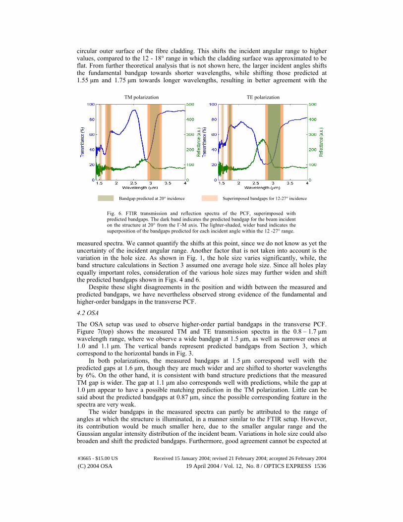
Figure 6 shows the FTIR spectra for TM and TE polarizations, where transmission and reflection are plotted in blue and green respectively. The vertical bands are the predicted bandgaps from Section 3, where each band represent the union of off-axis and out-of-plane bandgaps. Furthermore, the darker bands indicate predicted bandgaps for the average 20° incidence, while the lighter bands indicate the superposition of bandgaps for each angle in the 12 - 27° range. The lighter band representing the fundamental bandgap, at ~3.1 µm, is wider than the corresponding dark band by 51% and 37% for TM and TE polarizations respectively. The larger width ratios of the equivalent bands at shorter wavelengths are also self-evident, emphasizing the significance of the illumination of the structure from a range of angles.
For both polarizations we measure a strong bandgap in transmission at roughly 2.85 µm, falling within 10% of the predicted fundamental midgap. The measured TE gap appears wider and shifted towards shorter wavelengths compared to the TM, which is consistent with band structure predictions. Reflection peaks are also observed around these bandgaps, where their slight shift towards shorter wavelengths is due to the different focusing plane for this measurement (Fig. 2b). Nevertheless, they further emphasize the role of the PBG effect. Weaker bandgaps in transmission are also measured for both polarizations, at roughly 1.6 µm and 2 µm, which too falls within 10% of the predicted bandgaps.
One possible explanation of the shift between the measured and predicted bandgaps is the uncertainty in the angular range of the incident waves, which results from the refraction at the
Fig. 5. FDTD simulation geometry used to measurements.
Detector fibre
Input fi
PCF
PCF
Input fibre
Fig. 5. FDTD simulation geometry used to model the OSA measurements.
(C) 2004 OSA 19 April 2004 / Vol. 12, No. 8 / OPTICS EXPRESS 1535#3665 - $15.00 US Received 15 January 2004; revised 21 February 2004; accepted 26 February 2004
circular outer surface of the fibre cladding. This shifts the incident angular range to higher values, compared to the 12 - 18° range in which the cladding surface was approximated to be flat. From further theoretical analysis that is not shown here, the larger incident angles shifts the fundamental bandgap towards shorter wavelengths, while shifting those predicted at 1.55 µm and 1.75 µm towards longer wavelengths, resulting in better agreement with the
measured spectra. We cannot quantify the shifts at this point, since we do not know as yet the uncertainty of the incident angular range. Another factor that is not taken into account is the variation in the hole size. As shown in Fig. 1, the hole size varies significantly, while, the band structure calculations in Section 3 assumed one average hole size. Since all holes play equally important roles, consideration of the various hole sizes may further widen and shift the predicted bandgaps shown in Figs. 4 and 6.
Despite these slight disagreements in the position and width between the measured and predicted bandgaps, we have nevertheless observed strong evidence of the fundamental and higher-order bandgaps in the transverse PCF.
4.2 OSA
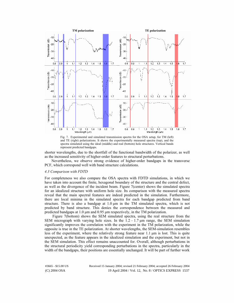
The OSA setup was used to observe higher-order partial bandgaps in the transverse PCF. Figure 7(top) shows the measured TM and TE transmission spectra in the 0.8 – 1.7 µm wavelength range, where we observe a wide bandgap at 1.5 µm, as well as narrower ones at 1.0 and 1.1 µm. The vertical bands represent predicted bandgaps from Section 3, which correspond to the horizontal bands in Fig. 3.
In both polarizations, the measured bandgaps at 1.5 µm correspond well with the predicted gaps at 1.6 µm, though they are much wider and are shifted to shorter wavelengths by 6%. On the other hand, it is consistent with band structure predictions that the measured TM gap is wider. The gap at 1.1 µm also corresponds well with predictions, while the gap at 1.0 µm appear to have a possible matching prediction in the TM polarization. Little can be said about the predicted bandgaps at 0.87 µm, since the possible corresponding feature in the spectra are very weak.
The wider bandgaps in the measured spectra can partly be attributed to the range of angles at which the structure is illuminated, in a manner similar to the FTIR setup. However, its contribution would be much smaller here, due to the smaller angular range and the Gaussian angular intensity distribution of the incident beam. Variations in hole size could also broaden and shift the predicted bandgaps. Furthermore, good agreement cannot be expected at
Fig. 6. FTIR transmission and reflection spectra of the PCF, superimposed with predicted bandgaps. The dark band indicates the predicted bandgap for the beam incident on the structure at 20° from the Γ-M axis. The lighter-shaded, wider band indicates the superposition of the bandgaps predicted for each incident angle within the 12 -27° range.
TM polarization TE polarization
Bandgap predicted at 20° incidence Superimposed bandgaps for 12-27° incidence
(C) 2004 OSA 19 April 2004 / Vol. 12, No. 8 / OPTICS EXPRESS 1536#3665 - $15.00 US Received 15 January 2004; revised 21 February 2004; accepted 26 February 2004
shorter wavelengths, due to the shortfall of the functional bandwidth of the polarizer, as well as the increased sensitivity of higher-order features to structural perturbations.
Nevertheless, we observe strong evidence of higher-order bandgaps in the transverse PCF, which correspond well with band structure calculations.
4.3 Comparison with FDTD
For completeness we also compare the OSA spectra with FDTD simulations, in which we have taken into account the finite, hexagonal boundary of the structure and the central defect, as well as the divergence of the incident beam. Figure 7(center) shows the simulated spectra for an idealized structure with uniform hole size. Its comparison with the measured spectra reveal that the main spectral features are indeed predicted in the simulation. Furthermore, there are local minima in the simulated spectra for each bandgap predicted from band structure. There is also a bandgap at 1.0 µm in the TM simulated spectra, which is not predicted by band structure. This denies the correspondence between the measured and predicted bandgaps at 1.0 µm and 0.95 µm respectively, in the TM polarization.
Figure 7(bottom) shows the SEM simulated spectra, using the real structure from the SEM micrograph with varying hole sizes. In the 1.2 – 1.7 µm range, the SEM simulation significantly improves the correlation with the experiment in the TM polarization, while the opposite is true in the TE polarization. At shorter wavelengths, the SEM-simulation resembles less of the experiment, where the relatively strong feature near 1.1 µm is lost. This is quite unexpected, as the feature appears in the idealized simulation and the experiment, but not in the SEM simulation. This effect remains unaccounted for. Overall, although perturbations in the structural periodicity yield corresponding perturbations in the spectra, particularly in the width of the bandgaps, their positions are essentially unchanged. It will be part of further work
Fig. 7. Experimental and simulated transmission spectra for the OSA setup, for TM (left) and TE (right) polarizations. It shows the experimentally measured spectra (top), and the spectra simulated using the ideal (middle) and real (bottom) hole structures. Vertical bands represent predicted bandgaps.
Experiment
Ideal simulation
SEM simulation
Experiment
Ideal simulation
SEM simulation
TM polarization TE polarization
(C) 2004 OSA 19 April 2004 / Vol. 12, No. 8 / OPTICS EXPRESS 1537#3665 - $15.00 US Received 15 January 2004; revised 21 February 2004; accepted 26 February 2004
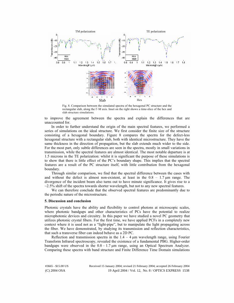
to improve the agreement between the spectra and explain the differences that are unaccounted for. In order to further understand the origin of the main spectral features, we performed a series of simulations on the ideal structure. We first consider the finite size of the structure consisting of a hexagonal boundary. Figure 8 compares the spectra for the defect-less hexagonal structure with a rectangular slab, both with identical microstructure. They have the same thickness in the direction of propagation, but the slab extends much wider to the side. For the most part, only subtle differences are seen in the spectra, mostly in small variations in transmission, while the spectral features are almost identical. The most notable departure is at 1.5 microns in the TE polarization: whilst it is significant the purpose of these simulations is to show that there is little effect of the PC’s boundary shape. This implies that the spectral features are a result of the PC structure itself, with little contribution from the hexagonal boundary.
Through similar comparison, we find that the spectral difference between the cases with and without the defect is almost non-existent, at least in the 0.8 – 1.7 µm range. The divergence of the incident beam also turns out to have minute significance. It gives rise to a ~2.5% shift of the spectra towards shorter wavelength, but not to any new spectral features.
We can therefore conclude that the observed spectral features are predominantly due to the periodic nature of the microstructure. 5. Discussion and conclusion
Photonic crystals have the ability and flexibility to control photons at microscopic scales, where photonic bandgaps and other characteristics of PCs have the potential to realize microphotonic devices and circuitry. In this paper we have studied a novel PC geometry that utilizes photonic crystal fibers. For the first time, we have applied PCFs in a completely new context where it is used not as a “light-pipe”, but to manipulate the light propagating across the fiber. We have demonstrated, by studying its transmission and reflection characteristics, that such a transverse fiber can indeed behave as a 2D PC.
Reflection and transmission spectra in the 1.4 – 4 µm wavelength range, using Fourier Transform Infrared spectroscopy, revealed the existence of a fundamental PBG. Higher-order bandgaps were observed in the 0.8 – 1.7 µm range, using an Optical Spectrum Analyzer. Comparing these spectra with band structure and Finite Difference Time Domain simulations
Fig. 8. Comparison between the simulated spectra of the hexagonal PC structure and the rectangular slab, along the Γ-M axis. Inset on the right shows a time-slice of the hex and slab structure simulations.
TM polarization TE polarization
HexSlab
(C) 2004 OSA 19 April 2004 / Vol. 12, No. 8 / OPTICS EXPRESS 1538#3665 - $15.00 US Received 15 January 2004; revised 21 February 2004; accepted 26 February 2004
gave compelling evidence that the observed spectral features were indeed due to the periodic nature of the fiber microstructure.
Based on a mature fiber-drawing technology [29, 30], the simple yet flexible fabrication of PCFs give the transverse fiber an advantage in many respects over existing PC fabrication technologies. For example, the smooth walls of a drawn fiber gives rise to five-orders-of-magnitude smaller scatter-based attenuation, compared to integrated waveguides [31]. This work may introduce a whole new fabrication paradigm whereby micro-photonic components are created using transverse optical fiber sections which have planar functionality designed into them at the draw stage. Further, the long air inclusions out of the plane provide a means to insert fluid into the optical interaction region to modify the response of the device [32]. In summary, we have proposed and demonstrated a new PC geometry. The comparatively simple fabrication of PCFs and its vast possibilities in the transverse geometry that are yet to be explored, makes fiber-based PCs a strong candidate for microphotonic applications.
Acknowledgments
This work was produced with the assistance of the Australian Research Council under the ARC Centres of Excellence program. CUDOS (the Centre for Ultrahigh bandwidth Devices for Optical Systems) is an ARC Centre of Excellence. MJS is supported in part by a NIST ATP grant through the Photonics CAD Consortium.
(C) 2004 OSA 19 April 2004 / Vol. 12, No. 8 / OPTICS EXPRESS 1539#3665 - $15.00 US Received 15 January 2004; revised 21 February 2004; accepted 26 February 2004