New Microsoft Word Document.docx
91
Assignment There are at least two different ways to characterize a material with electromagnetic simulation software: S-Parameter simulation and Eigenmode solution. S-Parameters In this assignment, we will find the S-parameters of a slab of Teflon by performing a time domain simulation. We will find these S-parameters with the default phase reference (incorrect) and with the phase reference de-embedded to the Teflon-vacuum interface (correct). Then we will compare the simulation results with an analytical formula. Launch CST Studio Suite (from the desktop.) Accept the university version agreement. Open CST Microwave Studio, the icon in the lower left corner. Then select Do no use a project template and click OK.
Transcript of New Microsoft Word Document.docx

Assignment
There are at least two different ways to characterize a material with electromagnetic simulation software: S-
Parameter simulation and Eigenmode solution.
S-Parameters
In this assignment, we will find the S-parameters of a slab of Teflon by performing a time domain simulation. We will
find these S-parameters with the default phase reference (incorrect) and with the phase reference de-embedded to
the Teflon-vacuum interface (correct). Then we will compare the simulation results with an analytical formula.
Launch CST Studio Suite (from the desktop.) Accept the university version agreement.
Open CST Microwave Studio, the icon in the lower left corner.
Then select Do no use a project template and click OK.

Let’s set up a few basic things, before we do any modeling.
Click the Home tab, then click Units on the command ribbon. Set the units to mm, GHz and ns (nano-seconds).
These will be most convenient units for the scale we will be working at.
Next select the Simulation tab, and click Frequency. Set the maximum frequency to 25 GHz.
Click Background. Set the background material to Normal, instead of PEC. The values for the background Epsilon
and Mue can be adjusted using the Properties... button, but just leave these values at unity. These are the material
properties relative to vacuum. So we are setting the background material to vacuum. (Note that the properties of air
are very close to vacuum.)
It’s a common mistake to omit this step and not realize that all the undefined regions in your simulation are the
default, PEC, that is a perfect electric conductor.
Now select the Modeling tab. Use the Brick tool to create a cube of Teflon, 10mm on side. The tool is a small cube on
the command ribbon.
Hit escape to pull up the numerical entry panel. Set the dimensions as shown and select [Load from Material
Library...] from the Material: menu. Load the lossy Teflon from the material library as shown.


The Teflon cube.

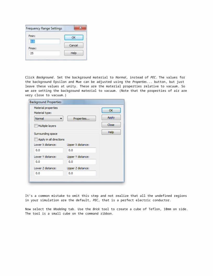
Let’s increase the lossiness of the Teflon to make the simulation results a bit more interesting. Double click the Teflon
material in the Materials folder of the Navigation Tree.

Select the Conductivity tab, and increase the tanδ by a factor of 500, to 0.1.

The resulting changed material properties versus frequency will be shown.
You can return to the 3D cad layout by clicking the 3D tab below the display window.
Next go back to the Simulation tab, and click Boundaries. Set the boundary conditions tomagnetic (Ht=0) on the two
X-planes, electric (Et=0) on the two Y-planes and open (add space)on the two Z-planes. This creates a TEM
waveguide, something difficult to do in the lab, but easy in simulation.
If you re-open the Boundaries panel, all the set boundaries will show color coded as follows.

By clicking Waveguide Port, create two waveguide ports. Use all default values, except choose Negative orientation
for the second one.


Now click Start Simulation, which will open the Time Domain Solver by default. (You can select other solvers on
the Home tab.) Set the Accuracy to -50 dB, the Source Type to Port 1 and check the Adaptive mesh refinement box.
Start the simulation.
Click Mesh View, so you can watch the adaptive mesh refinement as it proceeds. As the mesh refinement proceeds,
try different mesh view options to visualize the 3D structure of the mesh. Note that at the beginning of each
simulation, the ports are adaptively meshed before the volume is simulated.
Port 2 mesh.

Simulation domain volumetric mesh, Normal: X-plane shown.

You can also watch the convergence by viewing: 1D Results>>Adaptive Meshing>>S-Parameters>>S21 or S11 from
the Navigation Tree, on the left. The default view is the real part of the S-Parameter.
The simulation stops when the S-parameters converge. You will be asked if you want to disable further adaptive
meshing. Click yes.
The S-parameters represent the amplitude and phase of the reflected and transmitted waves relative to the incident
wave. The waves in question are the modes of the ports. It is very important to always look at the port modes to see if
they are as you think.
From the Navigation Tree select 2D/3D Results>>Port Modes>>Port 1>>e1. (Also look at h1 as well as Port 2.)

Now we want to export the magnitude and phase of just the final S-parameters (not all the adaptive passes). Click 1D
Results>>S-Parameters. Then click Polar in the 1D Plot tab.
Select the Post Processing tab, and click Import/Export. Then select Plot Data (ASCII)... and save the text file to an
appropriate location. The file should look like this:

Load the data into your favorite analysis package (e.g. MATLAB or Mathematica). Plot the linear magnitude of S11
and S21 (second column of file) versus frequency (first column of file). (Note that the S11 data is at the top of the file
and the S21 data begins half way down.) Make sure this plot looks like the S-parameter plot in Microwave Studio that
you get when you selectLinear from the 1D Plot tab.
You will also need the material properties for Teflon that were used in the simulation. In theNavigation Tree select 1D
Results>>Materials>>Teflon (PTFE) (lossy)>>Dispersive. Again, select the Post Processing tab, and
click Import/Export. Then select Plot Data (ASCII)... and save the text file to an appropriate location.
The resulting file will contain the real and imaginary parts of the Teflon permittivity, and the their ratio, tanδ. Note, that
CST uses the engineers’ convention for the time dependence of harmonic functions

and not the physicists’ convention
so that, for example, passive materials have a negative imaginary part. However, CST uses the primed and double
primed symbols to represent the real and negative imaginary part of a complex quantity
Also, tanδ is usually considered to be a positive quantity for passive materials, regardless of convention.
tanδ is a commonly specified material property that gives a measure of the lossiness of a material.
1. 1.Now plot the corresponding analytical result for the S-parameters using equation 1 and 2 ofthis article and the
material properties for Teflon that you exported from CST. For each S-parameter, put the curves for the simulation
and analytical results in the same graph for comparison. Adjust the styles and/or point density so both results can be
clearly seen.
Note that this is a physics article so that coefficients r and t’ are related to S11 and S21 through the complex conjugate
The wave vector, k, in equation 1 and 2 is the free space value and the speed of light in the units we are using is
about 300.
Also, d, is the thickness of the material, which is in our case 10mm. The refractive index, n, and the relative impedance, z, are related to the relative permittivity, ε, and the relative permeability,μ, in the usual way
Now lets see if the simulation and analytical results agree in phase as well as magnitude.

2. What is the significance of the frequencies at which S11 is a minimum? (Hint: consider the phase advance that a
wave undergoes making a round trip inside the Teflon slab.) Do these frequencies agree with the simple formula that
describes the condition? (You can use the nominal value of 2.1 for the permittivity of the medium for calculating the
wavelength or propagation constant.)
3. On one graph plot the real and imaginary parts of S11 versus frequency, both from simulation and equation 1 and
2. (Make sure you conjugate either the simulation or analytical results so that both use the same time harmonic function convention.) Make a second graph of this type for S21.
4. Explain why these results do not show agreement between simulation and analytical results.
Now we will fix the problem by de-embedding the simulation S-parameters. We will accomplish this by shifting the
port reference planes. The open (add space) boundary assignment has added some background media of thickness
equal to one eighth of the wavelength (in the background medium) at the center frequency (12.5 GHz). You can
check or change these settings by clicking the Open Boundary... button in the Boundary Conditions panel.

Now open the Waveguide Port panel by double clicking a port in the Navigation Tree.
Enter the correct value in the Distance to ref. plane box. (You may enter an expression that uses arithmetic operators
if you like.) A negative value moves the reference plane in toward the Teflon block. Make sure the reference plane
lies on the block as shown.

Do the same for the other port, then re-run the simulation and export the data. (The current mesh is fine. You don’t
need to re-run the adaptive meshing, so keep that box unchecked.)
5. Re-do the graphs, as in 2 above, with the new data. How is the agreement now?
Eigenmode Solution
From the Eigenmode Solver we can obtain the dispersion relation, that is the functional relationship between the frequency, ω, and the propagation constant, β. This relationship conveys a lot of information, particularly the phase
(and group) velocity, and thus the refractive index.
The Eigenmode Solver, can find this relationship for multiple bands, but we will look at just the lowest band. Lossy
(i.e. complex) and dispersive (i.e. frequency dependent) material properties significantly slow computation and
complicate the results, so we will use the default solver settings which ignore such properties. The Teflon will be
modeled as a material with a constant, real-valued, permittivity, of 2.1.
We won’t need the waveguide ports, in fact, they will cause an error, so we well delete them. In the Navigation Tree,
right click each port, to bring up the context menu, and select delete.

We wish to find frequencies for a range of values of the propagation constant. The way one specifies the propagation
constant is by using periodic boundary conditions with a Phase Shift. Change the boundary conditions on the faces
that used to have the ports to Periodic.
Then select the Phase Shift/Scan Angles tab and put in a variable for the Z phase shift. (I used th.) Click OK and
supply an initial value when prompted. Zero is fine.
Now, change the Solver type to Eigenmode. You can do this from the drop down menu on theHome tab.

Open the Eigenmode Solver Parameters panel by clicking Start Simulation.

We will leave all of these parameters at their default values, but we do need to set up aParameter Sweep, to simulate
a range of different values for the propagation constant. Click the Par. Sweep… button.
In the Parameter Sweep panel, click New Seq. and then New Par… . Choose the parameter you created from
the Name: menu, and specify 7 samples from 0 to 180 degrees, i.e. 30 degree steps.
Since the system will run multiple simulations, it does not, by default, save any results. To specify what is saved after
each simulation, click Result Template… .
From the top menu, select 2D and 3D Field Results, and then from the bottom menu select 3D Eigenmode Result.
The default setup parameters in this panel will save one eigenmode frequency, which is exactly what we want. Click
OK.

Now close the Template Based Postprocessing panel to return to the Parameter Sweep panel. Click Start to run the
seven simulations.
When the simulations are complete, find and select the Frequency (Mode 1) item in the Tablesfolder of
the Navigation Tree. Export this data as before.
6. 6.Plot a dispersion diagram (ω vs β) with the data points from the simulation and a theoretical curve for Teflon. Note
that the material properties used for the Eigensolver are non-lossy, non-dispersive properties. How well do the
simulation data points and the theory curve agree?
7. Does the dispersion diagram contain information about the refractive index and/or the impedance?


Assignment
In this assignment we will use the inverted theory, and extract material properties from S-parameters. We will do this both,
for a known material, Teflon, and a metamaterial with unknown properties, Teflon with Alumina spheres imbedded in it. We
already have the necessary S-parameters and Eigenmode simulation results for pure Teflon, so let’s do the simulations for
Teflon with Alumina spheres.
We will simulate just one unit cell of the proposed material, and the boundary conditions will ensure (in this case) that we are
finding the behavior of the bulk material.
Start where we left off with assignment 1, then insert the Alumina sphere into the Teflon. Click the Sphere tool, from the
Modeling Tab. Hit escape to bring up the Sphere panel. Define a sphere of 3mm radius located in the center of the Teflon
block. Load the material, Alumina (99.5%) (lossy) from the Library.
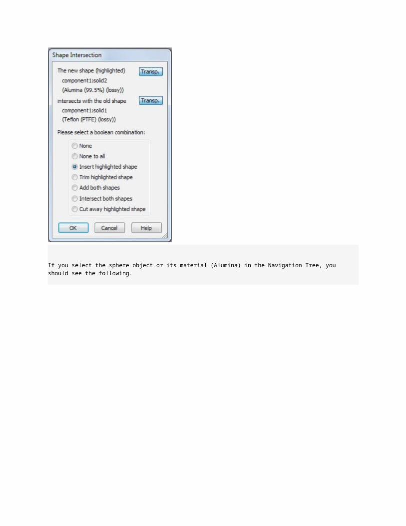
We now have material properties doubly specified where the Teflon and Alumina overlap. Microwave Studio wants to know
how to resolve this. Choose Insert highlighted shape.

If you select the sphere object or its material (Alumina) in the Navigation Tree, you should see the following.
Run the phase advance parameter sweep, as before. Select the Frequency (Mode 1) results from the Tables folder in the
Navigation Tree.
It seems the interesting part occurs between the last two data points. Let’s get some more data points in that range. Double
click the parameter entry in the Parameter Sweep panel, and change the sweep as follows.

Now Start the sweep again. This will add to your previous data without deleting it. Select the Frequency (Mode 1) results
again and export the data.
Now we want to get the S-parameters for our Alumina/Teflon metamaterial. We need to do several things to setup an S-
parameter simulation again. We need to: (1) return the z-boundaries to open (2) add some free space in the z-direction (3)
recreate two correctly reference ports (4) change the solver type back to time domain (5) change the mesh type back to
hexahedral and (6) adapt the mesh for the new material configuration.
Often times it makes more sense to add a specific amount of space to ports manual, then if any of the parameters that
determine the automatic add-space amount change, you won’t be surprised with in incorrectly referenced port. Use the brick
tool to create a Vacuum space the encompasses the teflon block and extends 5mm beyond it, on both sides, in the z-
direction.

To handle the intersection with the other objects, we want to Trim the vacuum block, with both the Teflon block and the
Alumina sphere.
Now we have to unconnected slabs of vacuum which are nevertheless one object.

Since we have handled the adding of space, change the boundaries to open.

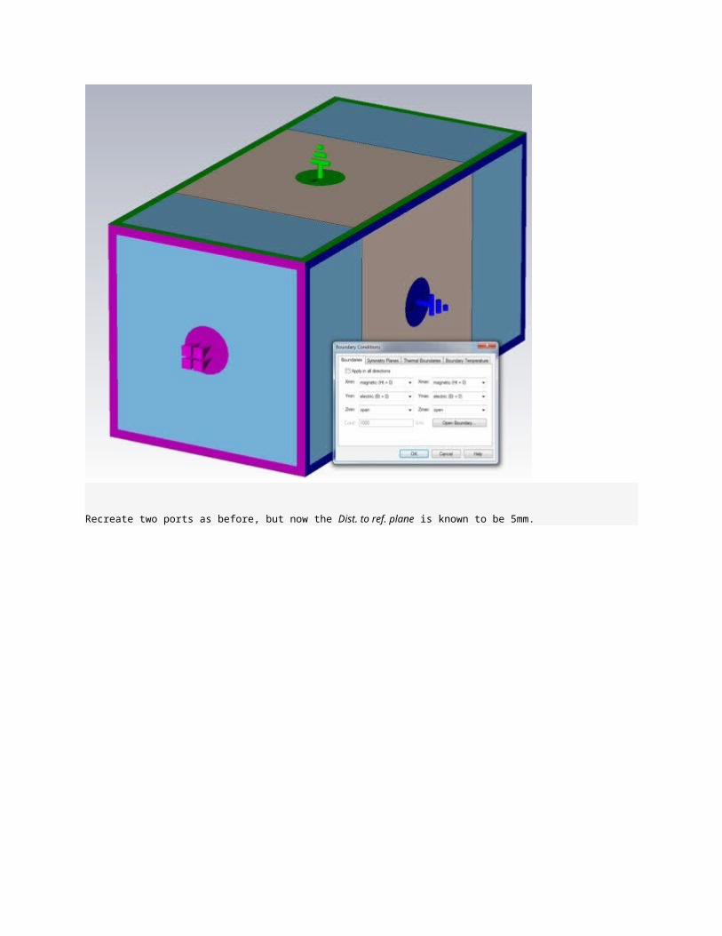
Recreate two ports as before, but now the Dist. to ref. plane is known to be 5mm.

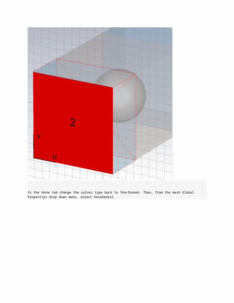
In the Home tab change the solver type back to Time Domain. Then, from the mesh Global Properties drop down menu,
select hexahedral.
This will open the Mesh-Properties - Hexahedral panel. The two primary control parameters: Lines per
wavelength and Lower mesh limit have been increased from their default values of 10 and 10 by your previous Mesh
Adaptation run. It is a good idea to perform a mesh adaptation after making significant geometric changes (like adding an
alumina sphere), but we mostly likely want to start from the 10, so change these values back to 10 and 10.
Now click Start Simulation to open the Time Domain Solver Parameters panel, check Adaptive mesh refinement, and
click Start.
Export the complex S-parameters as before (from the Polar view). Be sure not to over-write your previous S-parameters as
we are not finished with those yet.
For the uniform Teflon case do the following:
1. 1.Using the formulas from the Smith paper attempt to extract the material properties from the S-parameters. You
will first calculate n and Z, and then from them, mu and epsilon. Make branch corrections as discussed in class. Submit plots
comparing the real and imaginary part of the extracted mu and epsilon with the corresponding model properties used in the
simulation. Make one plot without branch corrections and one with. (For the permeability the model properties are 1+0*j.)
2. 2.How is the agreement?
For the metamaterial (alumina spheres in a Teflon matrix) do the following:
You might guess that an analytical model for the effective material properties exists for spherical inclusions, cubically
arranged in background medium. In fact there are many with varying degrees of sophistication. Perhaps the simplest is the
Maxwell-Garnett equation, equation 7 at this wikipedia link.
3. 3.Calculate the volume fraction of the alumina sphere.
4. 4.Use the exported Teflon properties, the silicon properties (which you can assume are constant and lossless) and the
volume fraction to calculate the Maxwell-Garnett effective permittivity. Also calculate the effective permittivity and
permeability from the simulation S-parameters using the Smith article equations as before. (You don’t have to bother with

branch correction on this part, though if you developed an automatic method, you can use. We will only be concerned with
the low frequency region where the default branch is correct.) Plot the real and imaginary parts of the permittivity versus
frequency for both these results on the same graph to compare. Make another graph for the permeability. (Since both the
block and sphere are non-magnetic, the Maxwell-Garnett permeability is, of course, 1+0*j ).
5. 5.How is the agreement between the S-parameter extracted results and the Maxwell-Garnett theory? Over what range of
frequencies do they agree? Do you expect agreement at low or high frequencies? Why?
6. 6.Calculate the real part of the permittivity from the eigenmode simulation, and add this to the plot above.
7. 7. Does this result agree well with the other two? Why, or why not?

Assignment
Simulate the ten different Split Ring Resonators (SRRs) in the article Metamaterial electromagnetic cloak at microwave
frequencies.
Start a new CST Microwave Studioproject and do not use a template. The units we have been using (mm, GHz and nS) are
probably a good choice. A frequency range of 0 to 25GHz willinclude the important features of the magnetic
and electric resonance. The boundary conditions should be chosen so that the magnetic flux of the TEM mode links the loop
of the SRR. If the SRR is oriented normal to the x-axis then the Xmin and Xmax boundaries should be magnetic.
The Ymin andYmax boundaries can then be chosen electric and the Zmin and Zmaxboundaries open. Use open instead
ofopen add space. Since we will need to add space around the resonator, we might as well add our own fixed amount of
space for the ports.
Set up the unit cell as shown below. All geometric parameters are given in the article. Use global variables for the geometric
features, r and s, that vary for the different designs. It will also be convenient to use a global parameter for the metal
thickness. Global parameters can be easily created by typing a valid variable name into the parameter entry fields when
defining an object. You will then be prompted to enter a default value.
Start with the substrate so it will be easier to tell that the resonator ring is being located in the right place. Choose Rogers
RT5870 (lossy) from the material library for the substrate and Copper (annealed)for the metal. Putting the origin at the
center of the ring, and at the substrate-metal interface, may make constructing the ring easier, but other choices are fine
obviously.

Construct the ring with square corners first then blend the edges later. You can draw a thin square slab for the ring and then
cut out the center regions and gap (using appropriate bricks and boolean operations), or draw individual ring segments as
bricks (making them into one object withModeling>>Boolean>>Add). In the later case, you can use the Mirror operation
underModeling>>Transform to create half the object for you.
Now select the edges to be blended (keyboard shortcut is e then double-click the edge). Select first the edges that will have
the interior radius, r (some of which are not shown below). You may want to make the object thicker to make it easier to
select the edges.
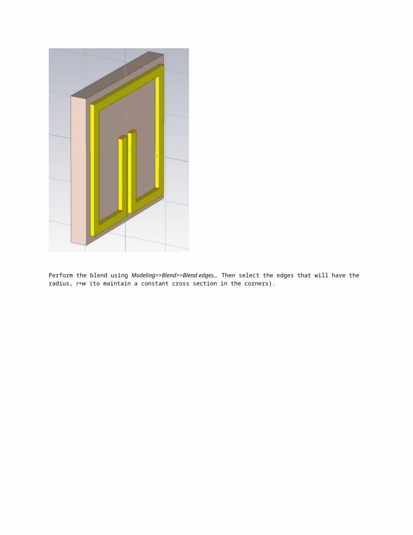
Perform the blend using Modeling>>Blend>>Blend edges... Then select the edges that will have the radius, r+w (to maintain
a constant cross section in the corners).

Perform the blend and return the object to its desired thickness of 0.017 mm.
Now add some vacuum around the SRR, including perhaps a unit cells length of space between the substrate and where
the ports will go. To resolve the intersecting shapes, you will need to trim highlighted shape for both the SRR and the
substrate. You may want to make the Vacuum material transparent so you can see the SRR even when it is not selected.
(Double click Materials>>Vacuum in the Navigation Tree to do this.)
Add the ports and be sure to adjust the port reference to the edge of the substrate.

The Adaptive mesh refinement will not give a satisfactory result for reasons I will explain in class. You should use 30/30 (or
higher) in the Mesh density control (Simulation>>Mesh>>Global Properties).

Open the Time Domain Solver Parameters, by clicking State Simulation. As usual, use -50dB for the accuracy and set the
source type to port 1 only. Click the Specials... button to bring up the Special Time Domain Solver Parameters panel. Select
the Steady State tab if it is not already selected. You need to extend the steady state time out condition. The simulation will
not reach the -50dB accuracy in 20 pulses. Make it 200 to ensure the simulation will run to the -50dB energy level.
Then select the General tab. For the sharp resonances we will see in the S-parameters, it would be better to
have more samples in your frequency range. Increase the Samples to 10,001. The frequency interval will then be
25GHz/10000 = 2.5 MHz. Click OK.

Then select Par. Sweep... to set up the simulation of all ten unit cell designs. Referencing your global parameters create a
sequence for each design, adding the two parameters, r and s, with appropriate values for each.

Next click the Result Template... button. Select S-Parameter from both the first and second menu.
Select Store all Available Port/Mode Combinations and Result Type All(complex). Then click OK and close the Template
Based Postprocessing window.

Click Start in the Parameter Sweep window to begin the simulations. It might take two or three hours to run all ten.
Export the S-parameters. If you can export each of the two data tables to separate files, while using the Polar display, you will have all of the S-parameter data. Extract the material properties ε and μ. Note that aθ is the correct extraction thickness.
You will probably not need to adjust the branch choice to obtain the correct results.
1. 1.Generate a plot for ε and a plot for μ. In each, plot the real part of the ten extracted material properties versus frequency.
Zoom the plot to display the region around the operating frequency, which we will take to be 8.55 GHz.
2. Also plot the real part of ε and μ versus radius, r, in the cloak at the operating frequency. The formula relating cloak radius
to cylinder number is
where a is the cloak inner radius (given in the article), i is the cylinder number and ar is the radial unit cell dimension (also
given in the article). In this plot versus radius, also include the desired analytical expressions for the material properties.
These are given in equation (3) in the article.
3. 3.An I-beam is a common metamaterial unit cell used for its providing an engineered permittivity:
http://www.nature.com/nmat/journal/v11/n5/pdf/nmat3278.pdf
Assume you have an I-beam unit cell that is well modeled by the Lorentzian

with parameters
so that at 10 GHz it provides a permittivity of
but you would like it to have a real part of permittivity of -1 and a small imaginary part. Suggest a quantitative change to
make to the I-beam that will make this happen.
You May Like×
The Healthy Eating Trends Of 2015The Daily Western
An Inside Look At The Newest And Most Amazing Cruise Ship In The WorldThe Daily Western

15 Of The Most Stunning Natural Waterfalls And Pools. Heaven On Earth.The Daily Western
8 Slow, Difficult Steps To Become A MillionaireThe Daily Western
10 Habits You Need To Adopt To Help Improve Mental HealthThe Daily Western

An Inside Look At The Craziest Airplane Cabins Of The FutureThe Daily Western
From Brazil To Japan, Fascinating Trip To Gas Stations From Around The...The Daily WesternWe think you'll find this interestingSponsoredAds By OffersWizard


Assignment
We will simulate something vaguely resembling an iPhone 4 antenna and determine its properties with and without a finger on the, so called, “death spot”.
First construct a model that captures the basic configuration of the handset’s antenna. It is possible that (as this person believes) the antennas are essentially slot antennas as outlined in an Apple patent.
Start a new project, without using a project template. Set up our usual units (mm, GHz, nS). Set the frequency range to 0 to 2 GHz. Set the Background Material to Normal with Epsilon = Mue = 1.
The innards (between the glass front and back) can be modeled as a single brick of metal. The outer-most part will be a steel band circumscribing the handset with two splits to create slot antenna boundaries. Use Copper (annealed) (lossy) for the innards and Steel-1010 (lossy) for the outer band, though obviously these are rough approximations. Use global parameters for all the geometric properties so we will have ample tuning capability. Use blend radii that lead to uniform cross-sections in the outer band and the slot.
Use global parameters and formulas to specify the geometry. For example:

For initial values use:exterior corner radius = 10mmlateral exterior dimensions use Apple tech specsmetal thickness = 6.3 mmglass thickness = 1.5 mmouter band width = 2.5 mmslot width = 2 mmleft lower slit position, below center = 43 mmleft upper slit position, left of center = 10 mmsplit width = 1 mm
Now add the glass to the front and back. Use Glass (Pyrex) (lossy) because we do not have a model for the fancy aluminosilcate glass that Mr. Jobs specified.

Set the glass back from the edge as on the real handset. For an initial value of the set back use 1 mm, and again, use blending radii such that all blends have the same center of curvature.
Set all boundaries to open (add space), since we want the antennas to radiate into an infinite space and we will not need to de-embed any waveguide ports. You may want to see where the simulation domain Bounding Box is. You can set this to be visible by checking Bounding Box in the View Tab.
Since our model of the handset is mirror symmetric, front-to-back, you can add one symmetry plane, for a 2X speed-up. Electric or magnetic? This symmetry plane must be compatible with the fields generated by the discrete port. Another way to think about it is to consider what would happen if you put zero impedance surface or a zero admittance surface at the proposed location.

Now add a discrete ports that will function as an antenna feed. Use the default 50 Ohms for the impedance (a guess).
The Discrete Edge Port panel is accessible from the Simulation Tab.

When selected the port is shown as a blue line with a red cone indicating the polarity. It should span the slot, and
should probably lie in the center (front to back) of the slot. For the initial value of the vertical posiiton of the feed,
choose 40mm below the center. You probably want to zoom in and hide the glass to confirm the port is where it ought
to be.


Now we can simulate. We will use the optimizer to find locations of the splits and feed that will maximize the antenna
efficiency. For the purpose of seeing the optimizer progress in a reasonable amount of time, we will prioritize speed
over accuracy. Open the Time Domain Solver Parameters panel. Leave the accuracy at -30dB. Under Specials... ,
increase the Number of pulses to a bigger number like 200, and give the frequency samples a modest boostto 4001
from 1001.
Now select Optimizer...
In the Parameter table select the variables controlling the locations of the feed and the splits, and give them the
biggest range that keeps the splits and feed on the straight portion of the band. Select one of the global optimization
algorithms. I used the Genetic Algorithm.
Select the Goals... tab, then Add New Goal..., and Result Template.... In the top menu select S-Parameters, and in
the bottom menu select S-Parameter. Click Mag. (lin) and then OK. Now select General 1D in the top menu and 0D

or 1D Result from 1D Result in the bottom menu. In the menu select x at Global y-Minimum, and S1,1mag for the 1D
result to be used. Then use a subrange of 1.5 to 2.
Click OK.
Select 1D Result from 1D Result in the bottom menu again. This time pick Global y-Minimum. Use the same
subrange.

Click OK. Then close the Template Based Postprocessing panel.
In the Define Optimizer Goal panel, select xAtGlobalYMin, and use the = operator, a variable for the Target, and 10
for the weight.
Click OK. Our frequency target will be a GSM band. Specifically, the middle of the
DCS-1800 Uplink band. http://en.wikipedia.org/wiki/GSM_frequency_bands
Add another goal for GlobalyMin.

Now click Start to begin the optimization. Each sim should take about 15 to 60 seconds. Let it run until you get a Sum
of all goals less than 0.5,
Now abort, and choose recalculate.

The best parameters will be displayed in the Optimizer Info tab, and with greater precision, in the Parameter List.
Record these values with a screen grab, in case something goes wrong.
Now, starting from these globally optimized parameters, use a local optimizing algorithm. For this, we want to
optimize the actual efficiency (instead of just minimizing S11), so we need to create a far-field monitor. From
the Simulation tab, select Field Monitor. Choose Farfield/RCS, and enter a variable for the Frequency.
For the frequency we will use the center of DCS-1800 Uplink band. To see the goals associated with this field monitor
in the optimizer, you need to run a simulation and get results for the monitor. Run a single simulation. Now, open the
optimizer, and add a new goal. ChooseEfficiencies/linear/Tot. Effic. [1] from the menu. Select the = operator and a
target of 1.

Click OK, the deselect the previous two goals, and select the new goal. Now adjust the parameter min max ranges on
the Settings tab. Use a range of about plus or minus 2 mm for around the globally optimized values, for each of the
three parameters. Switch to one of the local optimziaiton algorithm. I used the Trust Region Framework, for no better
reason than it is first in the menu.

You may want to clear the Tables before starting this new optimization. Use Delete Results in the Post
Processing tab. You will have to close the Optimizer panel to do this.
Start the optimizer. You should manage to reach a total efficiency of at least 0.75. If you are having trouble reaching
this goal, get help from me.
1. Provide a picture of the phone in the optimal configuration (with the glass hidden), and report the numerical
positions of the splits and feed with respect to the handset center.
2. 2.For the optimal configuration, report the fractional power distribution of the stimulated power, specifically report the
fractional power: reflected, radiated and absorbed. The absorbed power is whatever is left over from reflection and
radiation, and will include power absorbed in the copper, steel, and glass.

Of the absorbed power, what fraction was absorbed in the copper steel, and glass.
Now let us try to simulate the death grip. Get the electromagnetic properties of wet skin fromthis excellent website. In
particular get the conductivity and the relative permittivity of wet skin at our operating frequency. (We will assume
these properties are relatively constant over the GSM band.) Make a new material with these properties.

Put a cubic centimeter of this material centered on, and touching, the left-side split. Re-simulate.

3. 3.Report the power distribution as in question 2. What is the drop in radiated power (in dB) induced by touching the
split? Where is most of the power going, that is now not being radiated? Did the absorbed power go up or down?
Why?
Let’s add some local field monitors for both E and H. In particular, we want to look at our operating frequency and in
the plane of the slot.


Make sure your far field monitor is still present, and run one last simulation at the optimal configuration.
4. Include the following E and H plots of the slot fields in your report. Select from the navigation tree: 2D/3D
Results>>E-field>>e-field (f=fGSM,z=0)>>Abs. Then from the 2D/3D Plot tab clickProperties and then Plot
amplitude from the Phase/Animation selections. Back in the 2D/3D Plot tab, you can adjust the Clamp to
Range values to best display the field minima and maxima of the fields in the slot.
Do the same for the H-field.

Consider the magnitude of both E and H, and identify positions of maximum and minimum characteristic impedance
of the slot waveguide. Mark these locations on either your E or H plot (or both), with a ‘+’ and ‘-’ for maxima and
minima respectively. Is the feed point closer to an impedance minima or maxima? What is the approximate
impedance at the location of the feed? Is the impedance a maximum or minimum at the splits? What does this
suggest is the termination condition of the slot waveguide at the splits.?
5. Include a far-field plot in your report. Select from the navigation tree: Farfields>>farfield (f=fGSM). From the
Farfield Plot Properties, make the phone appear together with the radiation pattern. Include a couple views that
communicate most of the pattern geometry.


Describe two qualitative differences in the radiation pattern between this antenna and a dipole antenna. How does
this antenna’s directivity compare to that of a half-wave dipole antenna? How does the longest dimension of this
phone compare to the length of a half-wave dipole at our operating frequency?

Assignment
In this assignment we will construct a steerable metamaterial antenna, similar to the products being developed
by Kymeta. These are low-cost, steerable, high-gain satellite antennas that operate in the Ka band (26.5-40 GHz).
We begin by constructing a strip-line waveguide that serves as the feed for the antenna. We will use the low-loss
substrate, Rogers 3003. It is important to design with standard substrate and metal thicknesses, since changing
these thicknesses to arbitrary values is not economically feasible. The standard thicknesses are specified in the link.
Use the thickest substrate, and use the thinnest metal.
Use this calculator to determine the width, w, of the strip-line top trace for a 50 Ω impedance.
3.38
Use our standard units, mm, GHz and nS. Set the frequency to go from zero to the top of theKa band. Set
the Background to normal.
Create a section of microstrip along the z-axis with
where the initial value for N is 2 and the initial value for a is 1.11. Make the bottom conductor and substrate 3w wide.

Set the boundary conditions to open on the faces that are waveguide cross-sections, and open (add space) for the
other four boundaries.
Now add waveguide ports to both ends of the strip-line section. Simulate with the standard mesh (no adaptation) and
exciting just port 1.
Capture a plot of the port mode E field
and H field.

1. Are these the field patterns you expected for a strip-line? Qualitatively describe the associated currents and
charges. Can you use symmetry plane for these simulations? Which plane and what type?
2. Capture an S-parameter dB plot to include in your report. How would you describe the transmission characteristics
of this waveguide mode in this waveguide.
Now lets add a complimentary ELC resonator to the top strip. When formed from metal ELC resonators are designed
to respond to electric fields. When formed from the absence of metal in a metal plane, they respond to magnetic
fields. Be sure to orient your C-ELC so that the magnetic field can excite a resonance. Note that the resonance of the
ELC in the article is resonant around 15 GHz, since we want to resonate in the Ka band we want to scale the C-ELC
dimensions by some appropriate factor. Since one might want to adjust this later, create a scaling variable with an
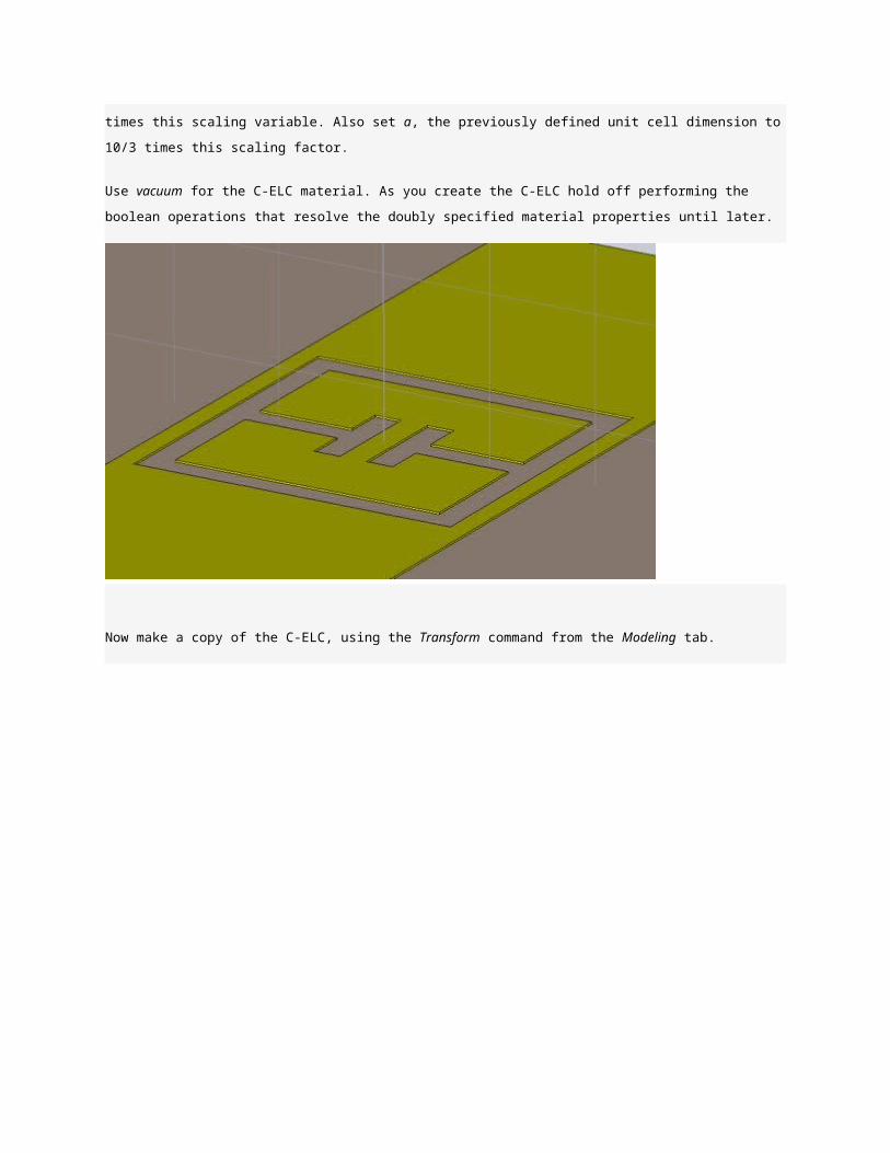
initial value of 1 and create the C-ELC with dimensions that are the original values (from the article) times this scaling
variable. Also set a, the previously defined unit cell dimension to 10/3 times this scaling factor.
Use vacuum for the C-ELC material. As you create the C-ELC hold off performing the boolean operations that resolve
the doubly specified material properties until later.

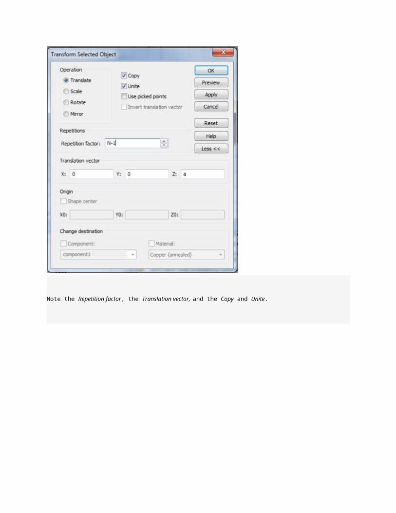
Now make a copy of the C-ELC, using the Transform command from the Modeling tab.
Note the Repetition factor, the Translation vector, and the Copy and Unite.

We want this to work even when N = 1. A repetition factor of 0 will give an error. Open the History List from the
Modeling Tab and find and edit the Transform command. Wrap an If statement around the Transform command.
Now perform a boolean operation to Subtract the C-ELC from the top trace.

Now set the scaling variable to 1/3
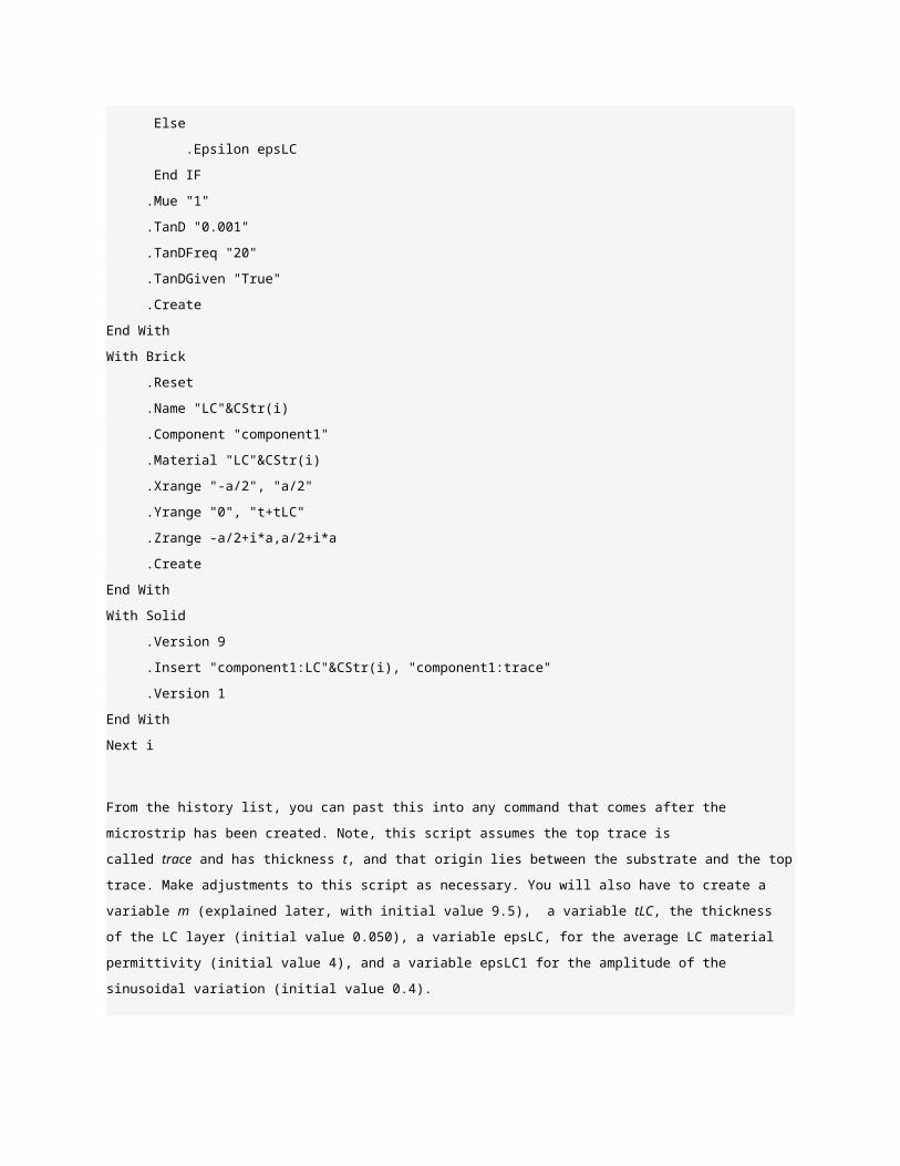
We want to add the liquid crystal layer. Use the following command script:
Dim i As Integer
For i = 0 To N-1
With Material
.Reset
.Name "LC"&CStr(i)
If N > 1 Then
.Epsilon epsLC+epsLC1*sin(i*m*pi/(N-1))
Else
.Epsilon epsLC

End IF
.Mue "1"
.TanD "0.001"
.TanDFreq "20"
.TanDGiven "True"
.Create
End With
With Brick
.Reset
.Name "LC"&CStr(i)
.Component "component1"
.Material "LC"&CStr(i)
.Xrange "-a/2", "a/2"
.Yrange "0", "t+tLC"
.Zrange -a/2+i*a,a/2+i*a
.Create
End With
With Solid
.Version 9
.Insert "component1:LC"&CStr(i), "component1:trace"
.Version 1
End With
Next i
From the history list, you can past this into any command that comes after the microstrip has been created. Note, this
script assumes the top trace is called trace and has thickness t, and that origin lies between the substrate and the top
trace. Make adjustments to this script as necessary. You will also have to create a variable m (explained later, with
initial value 9.5), a variable tLC, the thickness of the LC layer (initial value 0.050), a variable epsLC, for the average
LC material permittivity (initial value 4), and a variable epsLC1 for the amplitude of the sinusoidal variation (initial
value 0.4).
Set the repetition variable, N, to 1, so we can examine the properties of just one C-ELC.
Simulate again, but this time use adaptive meshing to try to find an adequate mesh, and set the accuracy to -50 dB.
Also, set the number of pulses to 200 as we have in the past to allow sufficient simulation time to reach this steady
state target. After the adaptation is complete, disable further adaptive meshing. (I converged to mesh properties of
25/25.)
3. Display and capture a plot of a mesh plane normal to the C-ELC, and zoomed in to that object. How many mesh
intervals span the C-ELC features? Does that seem adequate?
Now let’s see if this device radiates. Look at 1D Results>>Power>>Power Accepted. From this plot we can find the
frequency for peak accepted power, Pin. Use the command Move Axis Marker to Maximum to find this frequency.

Then create a Farfield monitor, and a E-field monitor both at this frequency. Choose a 2D plane for the E-field as
shown.
Simulate again an take a look at the E-field.
4. 4.Which cartesian component component is dominant in the waveguide propagation, and which looks most like it is
radiating? Is the latter consistent with a magnetic dipole oriented as you think it is?
Now do a parameter sweep with the liquid crystal permittivity. We are interested in the phase and magnitude of
radiation as a function of the liquid crystal permittivity. Set up template results for both of these.
Note we want the direction of radiation to be that of the ELC. Let the liquid crystal permittivity vary from 3 to 5 in
steps of 0.1
5. Provide a plot of phase (of the Theta component) vs the permittivity of the liquid crystal. You can screen grab this
from Microwave Studio. Identify the range of permittivity required to get the full range of phase available.
Use the above graph to determine the average (epsLC) and sinusoidal amplitude (epsLC1) that should be used to
create the permittivity periodicity. Set the global parameter values accordingly.
Now, increase the length of the device to 20 elements, by setting the value of N in the globaltable and performing an
update.

Perform a sweep of the parameter, m, which is proportional to the wave vector of the permittivity periodicity, kp, as
described in this article by Daniel Sievenpiper.
6. 6.Looking at the how m appears in the script above, what is the geometric interpretation of this parameter. For N =
20, what is the maximum value of m that will result in an un-aliased representation of the permittivity oscillation.
Perform the m sweep over the range of 1 to this maximum value. Use as many steps as you can manage, perhaps at
least 20 and no more than 100.
We want to save an antenna pattern at each value of the m sweep, so we can observe the radiation direction,
directivity and beam width. Before starting the sweep Add a step to theTemplate Based Postprocessing as follows.
Now analyze the results. We will try to find a a few of these antenna patterns that have good directivity and a good
range of angles.
7. 7.First find the maximum directivity and corresponding angle for each antenna pattern. Plot the maximum directivity
versus the angle of the maximum directivity for each pattern.
Your plot may look something like this:

Questions 8 and 9 are optional, but may be done for extra credit.
8. 8.Now pick the patterns with highest maximum directivity, every 25 degrees or so. and plot those patterns in the
same polar plot. Use a linear scale.
Your plot may look something like this:
9. 9.Make a plot similar to Figure 11 in Sievenpiper’s article, for the same set of antenna patterns you selected for the
directivity plot.
http://www.ece.utah.edu/~dschurig/7/ECE_5350_and_6350_Fall_2014/Assignments.html