New Interconnects - SNIA...9 • Arm’s DynamIQ and CoreLink CMN-600 technology • Cadence CCIX...
24
New Interconnects Moderator: Doug Voigt, Distinguished Technologist, HPE
Transcript of New Interconnects - SNIA...9 • Arm’s DynamIQ and CoreLink CMN-600 technology • Cadence CCIX...

New Interconnects
Moderator: Doug Voigt, Distinguished Technologist, HPE

© 2018 SNIA Persistent Memory Summit. All Rights Reserved.
Three Consortia Formed in Oct 2016
2

Cache Coherent Interface for Accelerators (CCIX)
David Koenen, Arm

© 2018 SNIA Persistent Memory Summit. All Rights Reserved.
CCIXTM cache coherent interconnect for accelerators
4
New class of interconnect for accelerated applications Mission of the CCIX Consortium is to develop and promote adoption of an industry standard specification to enable coherent interconnect technologies between general-purpose processors and acceleration devices for efficient heterogeneous computing.
https://www.ccixconsortium.com/

© 2018 SNIA Persistent Memory Summit. All Rights Reserved.
CCIX Consortium Inc
• Formed January 2016, incorporated in February 2017
• Complete ecosystem with 42 members and growing
• Hardware specification available for design starts for member companies
• CCIX pronounced: (c’ siks)

© 2018 SNIA Persistent Memory Summit. All Rights Reserved.
System topology examples
6
Accelerator
CCIX
Switch
Processor
CCIX
Processor
CCIX
Memory
CCIX
Memory
CCIX
Processor
CCIX
Accelerator
CCIX
Processor
CCIX
Accel
CCIX
CCIX
CCIX
CCIX Accel
CCIX
CCIX
CCIX
CCIX Accel
CCIX
CCIX
CCIX
CCIX Accel
CCIX
CCIX
CCIX
CCIX
Processor
CCIX
Processor
PCIe
Accel
CCIX
CCIX
CCIX PCIe
Accel
CCIX
CCIX
CCIX
PCIe
Accel
CCIX
CCIX
CCIX
CCIX Accel
CCIX
CCIX
CCIX
CCIX
Processor
PCIe
Direct attached, daisy chain, mesh and switched topologies

© 2018 SNIA Persistent Memory Summit. All Rights Reserved.
CCIX SoC to NVM Slave device
7

© 2018 SNIA Persistent Memory Summit. All Rights Reserved.
Shared Virtual Memory (Driverless) model used by CCIX
8
CCIX capable devices behave similarly to nodes in existing NUMA systems Memory based approach leverages existing Operating System capabilities Enabled by coherent shared virtual memory – it's all “just memory”
Dual mode CCIX/PCIe devices leverage PCIe Pins, Traces, Connector, and discovery
Minimal OS changes required, mostly for optional/enhanced capabilities E.G. one OS driver for power management, firmware-first error handling, etc. No Operating System drivers required for individual accelerators
Acceleration Framework (SW framework for offloading) Simple software library approach for applications running within VMs/Containers Developer writes regular application software in any language with full toolset

© 2018 SNIA Persistent Memory Summit. All Rights Reserved.
Arm CCIX demonstration vehicle
9
• Arm’s DynamIQ and CoreLink CMN-600 technology
• Cadence CCIX and PCIe controller and PHY IP • TSMC 7nm process technology • CCIX Connectivity to Xilinx’s Virtex UltraSoC+
FPGA
Xilinx, Arm, Cadence, and TSMC Announce World's First CCIX Silicon Demonstration Vehicle in 7nm Process Technology

© 2018 SNIA Persistent Memory Summit. All Rights Reserved.
CCIX: Seamless Acceleration
CCIX benefits accelerated applications such as machine learning, smart networks, and big data analytics with increased bandwidth, lower latency and more efficient data sharing Shared virtual memory enables CCIX accelerator functions that just work in the cloud Easy adoption and simplified development by leveraging today’s data center infrastructure
10

© 2018 SNIA Persistent Memory Summit. All Rights Reserved.
OpenCAPI Design Goals.
Low Latency High Bandwidth Attach Flexibility to support range of devices Asymmetric design, endpoint optimized for host and device attach

© 2018 SNIA Persistent Memory Summit. All Rights Reserved.
Memory Design Basis
POWER8 (2014) is origin of OpenCAPI memory attach IP Achieved 80 ns ”load to use” latency
Compared to 70 ns direct attach 4 DDR channels per buffer (32 socket)
Proprietary Non-standard lane width (21b) Slave only function
POWER8 Processor
DRAM Chips
DRAM Chips
Up to 8 Centaurs for each POWER8 Chip: 230 GB/s, 128 MB L4 Cache
Up to 4 DDR3 ports / Centaur (32 total): 410 GB/s, 1 TB memory

© 2018 SNIA Persistent Memory Summit. All Rights Reserved.
Comparison of Memory Paradigms
14
Needle-in-a-haystack Engine
Main Memory
Processor Chip
DD
R4/
5
Data DLx/TLx
Example: Basic DDR attach
Processor Chip DLx/TLx
Emerging Storage Class Memory
Processor Chip Data DLx/TLx
Tiered Memory
SCM
D
DR
4/5 Data DLx/TLx
SCM

© 2018 SNIA Persistent Memory Summit. All Rights Reserved.
POWER9 Hardware
25 GHz support Support for 32 lanes (four x8 interfaces) Bandwidth
22.1 GB/sec sustained read bw 22.0 GB/sec sustained write bw
Xilinx VU3P Device latency TL+DL running at 400 MHz Total send+receive latency of 80ns
Compared with ~400-500 ns for PCIe

© 2018 SNIA Persistent Memory Summit. All Rights Reserved.
OpenCAPI Consortium
• Open forum founded by AMD, Google, IBM, Mellanox, and Micron in October 2016 • Innovate and manage the OpenCAPI specifications/enablement and grow the ecosystem • Currently 35 members and steadily growing • Board Members: AMD, Google, IBM, Mellanox Technologies, Micron, NVIDIA, WD, and
Xilinx • Technical Steering Committee established with functioning Work Groups including PHY
Signaling, PHY Mechanical, TL Specification, DL Specification, Enablement, and soon Compliance and more
• Enablement in place for reference designs, documentation, SIM environment, etc. • Established website www.opencapi.org • Initial OpenCAPI Specifications available to download off website after registering
5

© 2018 SNIA Persistent Memory Summit. All Rights Reserved.
Cross Industry Collaboration and Innovation
17
OpenCAPI Protocol
Welcoming new members in all areas of the ecosystem
Systems and Software
Accelerator Solutions
ISVs
Research & Academic
Products and Services
Deployment
SOC

Gen-Z Memory
Michael Krause, HPE Gen-Z Lead Architect
www.genzconsortium.org
© 2018 SNIA Persistent Memory Summit. All Rights Reserved.
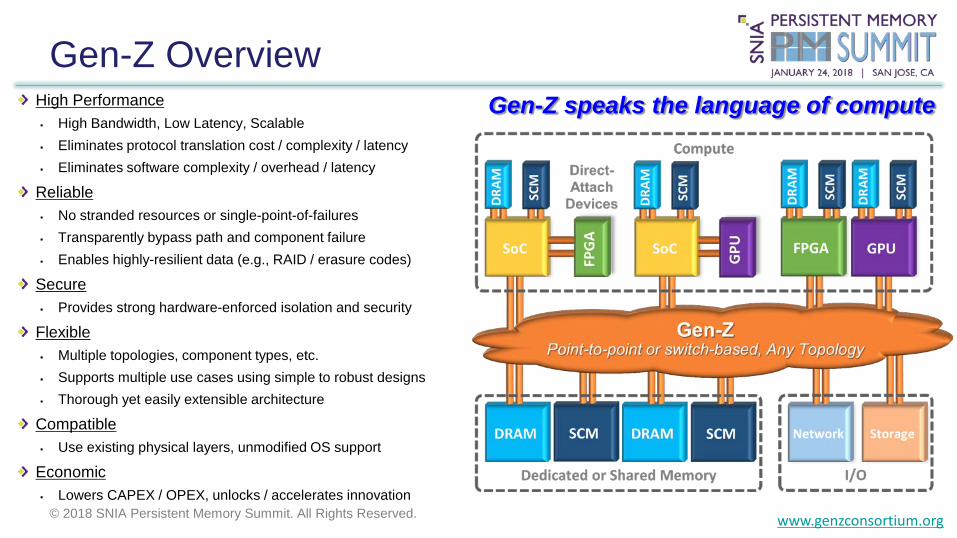
Gen-Z Overview High Performance High Bandwidth, Low Latency, Scalable Eliminates protocol translation cost / complexity / latency Eliminates software complexity / overhead / latency
Reliable No stranded resources or single-point-of-failures Transparently bypass path and component failure Enables highly-resilient data (e.g., RAID / erasure codes)
Secure Provides strong hardware-enforced isolation and security
Flexible Multiple topologies, component types, etc. Supports multiple use cases using simple to robust designs Thorough yet easily extensible architecture
Compatible Use existing physical layers, unmodified OS support
Economic Lowers CAPEX / OPEX, unlocks / accelerates innovation
Gen-Z speaks the language of compute
www.genzconsortium.org

© 2018 SNIA Persistent Memory Summit. All Rights Reserved.
Gen-Z Memory Use Case Seamlessly augments DDR / HBM solutions
Supports unmodified applications, OS, middleware Load-stores transparently translated into read-writes
Abstracts media to break processor-memory interlock Accelerates solution agility Creates a virtuous circle of innovation Supports any mix of DRAM, SCM, and NVM media
Very high bandwidth (16 GT/s to 112 GT/s signaling) Delivers 32 GB/s to 400+ GB/s per memory module
Supports legacy and new high-capacity form factors 10s GB to multi-TB capacities
Supports point-to-point and switch-based topologies Scales from co-packaged to single motherboard to rack-scale Flattens memory / storage hierarchy w/integrated resiliency, multipath, aggregation, etc. Logical PCI Device (LPD) scalability to 8192 modules (does not require NVMe-oF)
Built from the “ground up” to support persistent memory semantics Persistent Update (PU) flag applicable to multiple operation types
Write, Write Partial, Write Poison, Write-under-Mask, Meta Writes, Capabilities Write, Atomics, Buffer ops, Multi-Ops, LPD write / atomic operations, etc.
Persistent Flush—ensures all previously received modified data is persistent
www.genzconsortium.org

© 2018 SNIA Persistent Memory Summit. All Rights Reserved.
Composable Memory
Memory is captive of the host device (processor) Stranded memory channels and memory resources
Can’t scale memory independently of processing All accesses must traverse host processor
Today
Network / Fabric …
…
Gen-Z Memory and processing scale independently Heterogeneous compute & memory deployments Direct access to memory devices across fabric Memory can be dedicated or shared by processors Supports up to 64-way barber pole memory interleave—enables high-bandwidth DRAM and SCM solutions Supports RAID / erasure code-based memory solutions Scales from motherboard to rack-scale
www.genzconsortium.org

© 2018 SNIA Persistent Memory Summit. All Rights Reserved.
Scalable Form Factor (ZSFF)1
Supports any component type Flash, SCM, DRAM, NIC, GPU, FPGA, DSP, ASIC, etc.
Supports multiple interconnect technologies—Gen-Z, PCIe, etc. Single and double-wide—scale in x-y-z directions
Increased media, power, performance, and thermal capacity Double-wide can be inserted into pairwise single slots
Supports 1C, 2C, and 4C scalable connectors Density enables multiple connectors / module—scale power & performance
Scalable Form Factor Benefits: Simplifies supply chain Lower customer CAPEX / OPEX Consistent customer experience Increases solution and business agility @ lower dev cost Eliminates Potential ESD Damage
Can safely move modules from failed / old to new enclosure Eliminates SPOF and stranded resources
Multiple links per connector, multiple connectors per module Scalable thermal plus improved airflow across components Supports hybrid and data-centric computing
105 mm
154 mm
35.4mm
105 mm
1 Draft specification publicly available—see www.genzconsortium.org * Bandwidth calculated using 32 GT/s Signaling
** DRAM module provides 3.5x the highest-capacity DDR5 DIMM
76mm
© 2018 SNIA Persistent Memory Summit. All Rights Reserved.
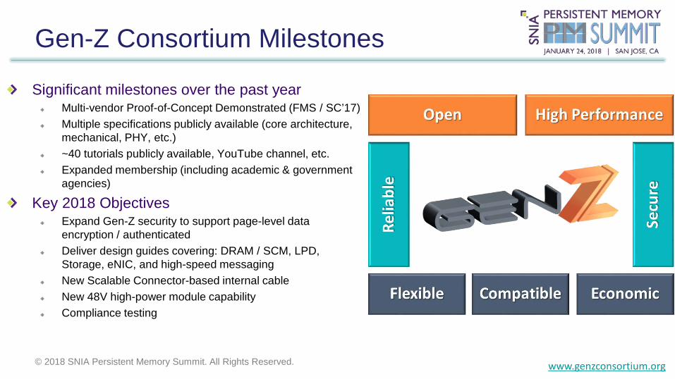
Gen-Z Consortium Milestones
Significant milestones over the past year Multi-vendor Proof-of-Concept Demonstrated (FMS / SC’17) Multiple specifications publicly available (core architecture, mechanical, PHY, etc.) ~40 tutorials publicly available, YouTube channel, etc. Expanded membership (including academic & government agencies)
Key 2018 Objectives Expand Gen-Z security to support page-level data encryption / authenticated Deliver design guides covering: DRAM / SCM, LPD, Storage, eNIC, and high-speed messaging New Scalable Connector-based internal cable New 48V high-power module capability Compliance testing
www.genzconsortium.org

Thank You