New Current Sensing Solutions for Low-Cost High-Power ...
188
New Current Sensing Solutions for Low-Cost High-Power-Density Digitally Controlled Power Converters Silvio Ziegler This thesis is presented for the degree of Doctor of Philosophy At The University of Western Australia School of Electrical, Electronic and Computer Engineering 2009
Transcript of New Current Sensing Solutions for Low-Cost High-Power ...

New Current Sensing Solutions for Low-Cost High-Power-Density
Digitally Controlled Power Converters
Silvio Ziegler
This thesis is presented for the degree of
Doctor of Philosophy At
The University of Western Australia
School of Electrical, Electronic and Computer Engineering 2009


iii
Abstract
This thesis studies current sensing techniques that are designed to meet the requirements
for the next generation of power converters.
Power converters are often standardised, so that they can be replaced with a model from
another manufacturer without an expensive system redesign. For this reason, the power
converter market is highly competitive and relies on cutting-edge technology, which
increases power conversion efficiency and power density. High power density and
conversion efficiency reduce the system cost, and thus make the power converter more
attractive to the customer.
Current sensing is a vital task in power converters, where the current information is
required for monitoring and control purposes. In order to achieve the above-mentioned
goals, existing current sensing techniques have to be improved in terms of cost, power loss
and size. Simultaneously, current information needs to be increasingly available in digital
form to enable digital control, and to allow the digital transmission of the current
information to a centralised monitoring and control unit. All this requires the output signal
of a particular current sensing technique to be acquired by an analogue-to-digital converter,
and thus the output voltage of the current sensor has to be sufficiently large.
This thesis thoroughly reviews contemporary current sensing techniques and identifies
suitable techniques that have the potential to meet the performance requirements of the
next-generation of power converters. After the review chapter, three novel current sensing
techniques are proposed and investigated:
1) The usefulness of the resistive voltage drop across a copper trace, which carries the
current to be measured, to detect electrical current is evaluated. Simulations and
experiments confirm that this inherently lossless technique can measure high
iv
currents at reasonable measurement bandwidth, good accuracy and low cost if the
sense wires are connected properly.
2) Based on the mutual inductance theory found during the investigation of the
copper trace current sense method, a modification of the well-known lossless
inductor current sense method is proposed and analysed. This modification
involves the use of a coupled sense winding that significantly improves the
frequency response. Hence, it becomes possible to accurately monitor the output
current of a power converter with the benefits of being lossless, exhibiting good
sensitivity and having small size.
3) A transformer based DC current sense method is developed especially for digitally
controlled power converters. This method provides high accuracy, large bandwidth,
electrical isolation and very low thermal drift. Overall, it achieves better
performance than many contemporary available Hall Effect sensors. At the same
time, the cost of this current sensor is significantly lower than that of Hall Effect
current sensors. A patent application has been submitted.
These three current sensing methods fulfil the requirements for the next generation of
digitally controlled power supplies that will have very high conversion efficiency, high
power density and decreasing cost per watt output power. The current sensing techniques
have been studied by theory, hardware experiments and simulations. In addition, the
suitability of the detection techniques for mass production has been considered in order to
access the ability to provide systems at low-cost.

v
In memory of my supervisor and friend Peter

vi
Table of Contents
ACKNOWLEDGEMENTS ...............................................................................................................IX
PUBLICATIONS...............................................................................................................................XI
STATEMENT OF CANDIDATE CONTRIBUTION ..................................................................XIII
LIST OF DIAGRAMS.......................................................................................................................XV
LIST OF TABLES.........................................................................................................................XXIV
CHAPTER 1: INTRODUCTION ....................................................................................................... 1
1.1 CURRENT SENSING – A VITAL TASK IN ALMOST EVERY APPLICATION ........................................................ 1
1.2 CURRENT SENSING IN POWER CONVERTER APPLICATIONS ............................................................................ 1
1.3 THE AC-DC CONVERTER EXAMPLE .................................................................................................................... 3
1.3.1 POWER-FACTOR-CORRECTION (PFC) STAGE..................................................................................... 4
1.3.2 DC-DC STAGE.......................................................................................................................................... 6
1.3.3 SUMMARY ................................................................................................................................................... 8
1.4 THESIS OUTLINE ....................................................................................................................................................... 8
CHAPTER 2: REVIEW OF LITERATURE ......................................................................................10
2.1 INTRODUCTION ....................................................................................................................................................... 10
2.2 CURRENT SENSING BASED ON OHM’S LAW OF RESISTANCE ......................................................................... 10
2.2.1 SHUNT RESISTOR .................................................................................................................................... 11
2.2.2 PRINTED-CIRCUIT-BOARD TRACE RESISTANCE SENSING ............................................................. 15
2.2.3 MOSFET SENSING ................................................................................................................................ 16
2.2.4 INDUCTOR CURRENT SENSING............................................................................................................ 19
2.2.5 CONCLUSION FOR CURRENT SENSOR BASED ON OHM’S LAW OF RESISTANCE ......................... 20
2.3 CURRENT SENSORS THAT EXPLOIT FARADAY’S LAW OF INDUCTION .......................................................... 20
2.3.1 ROGOWSKI COIL..................................................................................................................................... 21
2.3.2 CURRENT TRANSFORMER ..................................................................................................................... 23
2.4 CURRENT SENSING BY MEANS OF MAGNETIC FIELD SENSORS..................................................................... 26
2.4.1 SENSING CONFIGURATIONS................................................................................................................. 27
2.4.2 MAGNETIC FIELD SENSORS.................................................................................................................. 32
2.4.3 CONCLUSION FOR MAGNETIC FIELD SENSORS................................................................................ 44

vii
2.5 CURRENT SENSORS THAT USE THE FARADAY EFFECT ................................................................................... 44
2.5.1 POLARIMETER DETECTION METHOD................................................................................................ 45
2.5.2 INTERFEROMETER DETECTION METHOD ........................................................................................ 47
2.5.3 CONCLUSION FOR FARADAY EFFECT BASED CURRENT SENSORS ................................................ 51
2.6 DISCUSSION.............................................................................................................................................................. 51
2.6.1 SUMMARY ................................................................................................................................................. 56
CHAPTER 3: CURRENT SENSING USING THE COPPER TRACE RESISTANCE ..................58
3.1 INTRODUCTION....................................................................................................................................................... 58
3.2 PROPOSED METHOD .............................................................................................................................................. 59
3.3 STATIC PERFORMANCE .......................................................................................................................................... 60
3.3.1 TEMPERATURE SENSING REQUIREMENTS ........................................................................................ 61
3.3.2 TEMPERATURE ISOLATION OF THE SENSOR ..................................................................................... 62
3.3.3 MEASUREMENT RESULTS...................................................................................................................... 65
3.3.4 COMPARISON OF THE TWO CORRECTION TECHNIQUES................................................................ 66
3.4 CALIBRATION PROCEDURE................................................................................................................................... 67
3.5 DYNAMIC PERFORMANCE ..................................................................................................................................... 69
3.5.1 MUTUAL INDUCTANCE THEORY ......................................................................................................... 69
3.5.2 SIMULATION RESULTS ........................................................................................................................... 72
3.5.3 COMPENSATION NETWORK ................................................................................................................. 74
3.5.4 FREQUENCY RESPONSE VERIFICATION............................................................................................. 75
3.5.5 TIME-DOMAIN MEASUREMENTS......................................................................................................... 76
3.5.6 ADDITIONAL CONSIDERATIONS ......................................................................................................... 77
3.6 SUMMARY.................................................................................................................................................................. 77
CHAPTER 4: A METHOD TO IMPROVE THE LOSSLESS OUTPUT INDUCTOR CURRENT
SENSE METHOD .............................................................................................................................79
4.1 INTRODUCTION....................................................................................................................................................... 79
4.2 THEORY .................................................................................................................................................................... 81
4.2.1 CONVENTIONAL METHOD................................................................................................................... 81
4.2.2 PROPOSED METHOD OF COUPLED SENSE WINDING..................................................................... 82
4.3 EXPERIMENTAL RESULTS ...................................................................................................................................... 86
4.4 SUMMARY.................................................................................................................................................................. 89
CHAPTER 5: A SIMPLE AND ACCURATE TRANSFORMER BASED CURRENT SENSOR ... 91
5.1 INTRODUCTION....................................................................................................................................................... 91
5.2 THE CIRCUIT PROPOSED BY SEVERNS ................................................................................................................ 92
5.2.1 LIMITATIONS OF THE SEVERNS CIRCUIT ........................................................................................... 98
5.3 CIRCUIT MODIFICATIONS THAT EXTEND THE MEASUREMENT RANGE ................................................... 101
5.3.1 CONSTANT AUXILIARY CURRENT ..................................................................................................... 101
5.3.2 PULSED AUXILIARY CURRENT........................................................................................................... 109
5.3.3 POWER CONSUMPTION AND MEASUREMENT BANDWIDTH ........................................................ 112
5.3.4 COMPARISON......................................................................................................................................... 118
5.4 ELECTRICAL ISOLATED VOLTAGE SENSOR ..................................................................................................... 118

viii
5.5 PRACTICAL CONSIDERATIONS ............................................................................................................................121
5.5.1 LINEARITY ERROR................................................................................................................................122
5.5.2 THERMAL DRIFT ...................................................................................................................................128
5.5.3 ADDITIONAL CONSIDERATIONS .......................................................................................................131
5.6 SUMMARY ................................................................................................................................................................139
CHAPTER 6: CONCLUSIONS........................................................................................................142
6.1 PROBLEM SUMMARY .............................................................................................................................................142
6.2 COPPER TRACE CURRENT SENSE APPROACH..................................................................................................142
6.3 OUTPUT INDUCTOR CURRENT SENSING WITH COUPLED SENSE WINDING.............................................143
6.4 MODIFIED SEVERNS CIRCUIT .............................................................................................................................143
6.5 FUTURE RESEARCH...............................................................................................................................................145
6.5.1 SENSING PRINCIPLES BASED ON OHM’S LAW OF RESISTANCE ...................................................145
6.5.2 MODIFIED SEVERNS CIRCUIT ............................................................................................................145
BIBLIOGRAPHY..............................................................................................................................149
APPENDICES ..................................................................................................................................159
THE HISTORY OF CURRENT SENSING ..........................................................................................................................159
THE BEGINNINGS .................................................................................................................................................159
PROGRESS MADE WITHIN THE LAST FIFTY YEARS........................................................................................162
SUMMARY ................................................................................................................................................................163

ix
Acknowledgements
A doctoral thesis demands a great deal of effort and persistence from the candidate.
However, I found that research is most efficient if theories, results and findings can be
discussed with other scholars. From that point of view, the quality of supervision is crucial
in order to complete a PhD within reasonable time. I was very lucky being supervised by
four people with very different backgrounds who each played an important role during the
time of my candidature.
First, I have to thank my coordinating supervisor Dr. Herbert H.C. Iu, who always pushed
me to produce written work and to meet timelines. Moreover, without him it would have
been impossible to manage all the administrative work during the time I was overseas.
Secondly, I am much in debt to Dr. Robert Woodward from physics department, who
became a supervisor of mine in my second year. Useful as it turns out, as the thesis
contains a lot about magnetics. Robert always challenged my theories and findings and
many times helping to keep me on track by pointing out mistakes in my theories that are
notoriously very difficult to find by the person who developed them.
My third supervisor, Dr. Lawrence Borle, was initially my coordinating supervisor but then
left the university after my first year to pursue opportunities in the private industry.
Nevertheless, he played an important role during my candidature by discussing my ideas,
proofreading written work and teaching me the shortest way from Leederville train station
to the university by bike through Kings Park.
A very valuable supervisor was also Peter Gammenthaler from the company Power-One
Switzerland. He was the person who pointed out the potential of the transformer based
DC current sensor discussed in Chapter 5. Thanks to him and the company Power-One it
became possible to submit a patent application in the US. Tragically, he never saw the final
thesis since he suffered a stroke one week after his fiftieth birthday. I also have to thank

x
Alain Chapuis from Power-One who proofread the patent application and made valuable
suggestions. Moreover, I have to thank the company itself for supporting my studies.
Although a dissertation is all about the research outcome, the whole process would be
incredible isolating and endless without having exceptional lab mates and friends like
Hamdan, Eric, Chin Wea and Gillian. I very much enjoyed the profound discussions and
think we learned a lot about different cultures from each other. Finally, I want to thank my
girlfriend Miriam who was willing to spend such a long time together with me in Australia
far away from our friends and families.

xi
Publications
Fully refereed journal articles
1. S. Ziegler (70 %), R. C. Woodward, H. H. C. Iu, and L. J. Borle, "Lossless inductor
current sensing method with improved frequency response," IEEE Transactions
on Power Electronics, vol. 24, pp. 1218−1222, 2009.
2. S. Ziegler (70 %), R. C. Woodward, H. H. C. Iu, and L. J. Borle, "Investigation into
static and dynamic performance of the copper trace current sense method," IEEE
Sensors Journal, vol. 9, pp. 782−792, 2009.
3. S. Ziegler (60 %), R. C. Woodward, H. H. C. Iu, and L. J. Borle, "Current sensing
techniques: A review," IEEE Sensors Journal, pp. 354−376, 2009.
4. S. Ziegler (80 %), L. Borle, and H. H. C. Iu, "Transformer based DC current sensor
for digitally controlled power supplies," Australian Journal of Electrical &
Electronics Engineering (AJEEE), vol. 5, pp. 245−253, 2008.
Conference papers (Key: # digest review,* peer review)
5. (#) S. Ziegler (70 %), H. H. C. Iu, R. C. Woodward, and L. J. Borle, "Theoretical
and practical analysis of a current sensing principle that exploits the resistance of
the copper trace," in 39th IEEE Power Electronics Specialists Conference,
PESC'08. Rhodes, Greece, 2008, pp. 4790-4796.
6. (*) S. Ziegler (80 %), L. Borle, and H. H. C. Iu, "Transformer based DC current
sensor for digitally controlled power supplies," in Australasian Universities Power
Engineering Conference 2007. Perth, Australia, 2007, pp. 525-530.
7. (*) S. Ziegler (80 %), L. J. Borle, and H. H. C. Iu, "Digital current control
techniques for DC-DC converters," in The Eight Postgraduate Electrical

xii
Engineering & Computing Symposium, PEECS 2007. Perth, Australia, 2007, pp.
34-38.
Patents
8. S. Ziegler (70 %), P. Gammenthaler, and A. Chapuis, "An isolated current to
voltage, voltage to voltage converter," U. S. P. T. Office, Ed. USA: Power-One
Inc., 2008 (Application submitted).

xiii
Statement of candidate contribution
This thesis is based upon work I and a number of co-authors have published between 2007
and 2009. However, I developed the fundamental principles, theories, and carried out the
hardware experiments for the above-mentioned publications.
The contributions of this thesis are in particular:
1. In Chapter 2 a thorough review of state-of-the-art current sensing technologies is
given. This review acknowledges the fact that particular equations and performance
data are seldom directly applicable onto a certain problem and a basic
understanding of the working principle is required. This is achieved by discussing
the underlying physical principles rather than just reflecting performance data and
equations. It should help students and engineers to gain a broader knowledge of
different current sensing techniques and empower them to select the right
technique to solve a specific current sensing problem. This Chapter is based on up
to 70 % on Publication 3.
2. In Chapter 3, the usefulness of the temperature compensated copper trace current
sense method has been verified by theory and hardware experiment. The
experiments revealed that thermal isolation between temperature sensor and copper
trace leads to an underestimation of the busbar temperature. Compensation
techniques have been proposed to eliminate this measurement error. Hardware
experiment also showed that the parasitic inductance seen by the sense wires is
given by the mutual inductance between the main current loop and sense loop.
Consequently, the measurement bandwidth of this current sense method is
determined by the geometrical arrangement of copper trace and sense wires. Based
on this theory, a compensation network has been proposed to notable enhance the
measurement bandwidth of this method. This Chapter coincides with
approximately 90 % of Publication 2.

xiv
3. Chapter 4 shows that the mutual inductance theory developed in Chapter 3
provides a fine solution and notably improvement to the frequency response of the
established output inductor current sensing method, which exploits the winding
resistance of the output inductor. The mutual inductance theory of Chapter 3
predicts that this inductor can be supplemented with a coupled sense winding to
increase the inherent measurement bandwidth. A hardware experiment yielded two
decades improvement in measurement bandwidth due to the coupled sense
winding principle. Up to 90% of this Chapter was published in Publication 1.
4. The literature review of Chapter 2 revealed a simple transformer based current
sensing technique proposed twenty years ago with low-cost and high accuracy.
However, this technique does not allow measurement of currents down to zero
amps. Chapter 5 discusses a simple extension of the twenty years old circuit that
makes it possible to measure currents down to zero amps. Multiple circuit variants
are investigated and theoretically compared against each other. The high
measurement accuracy is also confirmed using hardware experiments. This chapter
further investigates non-ideal characteristics of the proposed current sense method
like thermal drift, non-linearity and stray magnetic field immunity. It has been
found that thermal drift and non-linearity can be solely described by the
characteristic of the employed magnetic core material. Local saturation effects, due
to external magnetic stray fields and non-centred primary conductor, have been
investigated as well. These investigations indicate a trade-off between magnetic
noise immunity, primary conductor position and magnetic core size. This Chapter
is partially based on Publications 4, 6 and 8 (~25 %).

xv
List of diagrams
Figure 1-1: Conventional two-stage AC-DC converter design ................................................. 4
Figure 1-2: AC-DC power converter efficiency and power density trend............................... 4
Figure 1-3: Current sensing in a PFC stage.................................................................................. 5
Figure 1-4: Current sensing in an isolated full-bridge DC-DC conversion stage................... 6
Figure 2-1: Current Equivalent circuit diagram for a shunt resistor....................................... 11
Figure 2-2: Impedance measurement of a typical SMD shunt resistor (WSL2512, 3 mΩ -
image courtesy of Vishay Dale Inc.)............................................................................................. 12
Figure 2-3: Bandwidth and voltage drop of shunt resistors based on a series of exemplary
SMD resistors at a power dissipation of 1 W.............................................................................. 13
Figure 2-4: A dedicated sense connection can overcome the problem with the high
temperature coefficient of the resistance at the soldering points (Photo courtesy
Isabellenhuette GmbH).................................................................................................................. 14
Figure 2-5: The voltage drop across the MOSFET Q2 that is connected to ground can be
used to measure currents. The strong thermal drift of RDSon and its unit-to-unit variation
limit the practicality of this principle. ........................................................................................... 16
Figure 2-6: Some MOSFETs provide a so-called sense connection, which carries a small
percentage of the current that flows though the drain connection of the MOSFET. To
avoid measurement errors, a small voltage drop between sense and Kelvin terminal has to
be ensured by means of an operational amplifier circuit........................................................... 18
Figure 2-7: The parasitic series resistance R of the output inductor L inside a power
converter can be used as a lossless measurement of the output current. A low-pass circuit
(R1, C1) that has its time constant matched with the inductance L and its series resistance R
filters out the voltage across the inductance L. .......................................................................... 19

xvi
Figure 2-8: Schematic of a Rogowski coil that uses a nonmagnetic core material. An
integrator is required to get a signal proportional to the primary current ic from the induced
voltage. ..............................................................................................................................................21
Figure 2-9: The influenced of the conductor position on the accuracy of the Rogowski
coil......................................................................................................................................................22
Figure 2-10: Current / Frequency limits of Rogowski coils. Rigid coils have the advantage
of being able to measure at smaller frequencies, whereas flexible coils have improved
handling capability, and usually can measure at higher frequencies. ........................................23
Figure 2-11: A current transformer consisting of one primary turn and multiple secondary
turns so as to reduce the current flowing on the secondary side (Image courtesy Power-
One Inc). ...........................................................................................................................................24
Figure 2-12: Equivalent circuit diagrams for current transformers (a) includes a
magnetizing inductance Lm, which requires the mean voltage applied to the transformer
winding to be zero, or the transformer saturates. The secondary winding capacitance Cw
limits the bandwidth, especially at high number of secondary turns. (b) CT where diodes
D1- D3 allow the transformer to demagnetize during the off-time and protect the sense
circuitry that acquires the voltage across Rs. ................................................................................25
Figure 2-13: Output voltage vs. duty cycle for a CT. Due to the droop effect, the linearity
of the current transformer is degraded at high duty cycle or current pulse with large on-
times (vout is the low-pass filtered sense voltage vs). The method proposed by McNeill et al.
reduces the excursion of the flux within the magnetizing inductance, and thus leads to a
superior linearity [37].......................................................................................................................26
Figure 2-14: The simplest schematic for open-loop current measurement. It uses a
magnetic field sensor that directly measures the magnetic field around the current carrying
conductor. External magnetic fields significantly deteriorate the accuracy of this technique.
............................................................................................................................................................27
Figure 2-15: Schematic for an open-loop current sensing configuration using a magnetic
core to concentrates the field from the primary conductor onto the magnetic sensor. This
not only increases the sensitivity of the current sensor due to the permeability of the core
material but decreases the sensitivity to external magnetic fields. ............................................28
Figure 2-16: A degaussing cycle, which consist out of a sinusoidal decreasing
demagnetization current, is used to retrieve the initial operation point of the magnetic core
material after an overcurrent incident...........................................................................................29

xvii
Figure 2-17: A closed-loop configuration in which a secondary winding is used to
compensate the flux inside the transformer to zero, while the output voltage of the
magnetic field sensor acts as an error signal. The current through the secondary winding
can be measured to determine the magnitude of ic..................................................................... 30
Figure 2-18: Use of the secondary winding of a closed-loop configuration as a current
transformer to achieve high bandwidth. ...................................................................................... 31
Figure 2-19: A closed-loop configuration not using a magnetic core employs a Wheatstone
bridge built with magnetic field sensors that measures the superposition of the magnetic
fields between the primary current, and the compensation current Icomp. The compensation
current is adjusted until its magnetic field compensates the field of the primary current.
When the magnetic fields compensate each other, the compensation current provides a
measure for the primary current (Image courtesy Sensitec GmbH)........................................ 31
Figure 2-20: A schematic of the Eta technology, which combines the output of an open-
loop Hall-effect sensor and a current transformer to achieve a high bandwidth current
transducer. This greatly reduces the power consumption and enables the use of a 5 V
supply voltage compared with ±15 V for closed-loop sensors. ............................................... 32
Figure 2-21: Due to the Lorentz law, a flowing current I through a thin sheet of
conductive material experiences a force if an external magnetic field B is applied.
Therefore, at one edge of the sheet the density of conductive carrier is higher, resulting in a
voltage potential v that is proportional to the magnetic field B................................................ 33
Figure 2-22: The Vacquier fluxgate principle: A sinusoidal current i0 periodically drives the
core magnetization from positive to negative values, and thus changes the differential
permeability seen by the external field Hext. The voltage vs induced into the pick-up winding
is measured to determine the magnetic field Hext. ...................................................................... 35
Figure 2-23: The fluxgate method takes advantage of the fact that the permeability µ of a
magnetic core material depends on the applied magnetic field................................................ 36
Figure 2-24: The fluxgate principle can be used in different ways to measure currents. a) In
a closed or open-loop configuration where the magnetic field sensor is represented by the
fluxgate. b) Low frequency version using a closed toroid core without pick-up winding. c)
Additional current transformer to extend the bandwidth. d) Having a third core to oppose
the voltage disturbance introduced into the primary conductor by the first fluxgate........... 37
Figure 2-25: Thermal drift of a 15 A current sensor based on the fluxgate technology
described in 5.3.2 (Amorphous core material, 100:1 turns ratio). ............................................ 37

xviii
Figure 2-26: An AMR Sensor consisting of aluminum is vaporized onto a permalloy strip
in a 45° angle against the intrinsic magnetization M0 so as to cause the current I to flow at
45° to M0 because of the much lower resistance of aluminum compared with permalloy...39
Figure 2-27: The change in resistance of an AMR sensor as a function of the angle
between the current I and the magnetization M. An external magnetic field Hext causes a
change in the direction of M, which is the superposition between M0 and Hext.....................40
Figure 2-28: The output voltage as a function of external magnetic field for an AMR
sensor. By applying an auxiliary magnetic field Hx along initial direction of magnetization of
the permalloy strip (M0) it is possible to adjust the field sensitivity of the sensor and
suppress saturation effects..............................................................................................................40
Figure 2-29: Frequency response of a commercial available AMR current sensor (Image
courtesy Sensitec GmbH)...............................................................................................................41
Figure 2-30: Basic working principle of the GMR Effect: a) At zero external magnetic field
Hext, the resistance R(0) appears at the input leads. b) A magnetic field Hext that points into
opposite direction as the intrinsic magnetization of the pinned ferromagnetic layer
increases the resistance. c) The opposite happens if Hext points into the same direction as
the pinned ferromagnetic layer’s magnetization. d) The intrinsic magnetization of the
pinned ferromagnetic layer can be permanently changed by applying a strong external
magnetic field Hext. ...........................................................................................................................42
Figure 2-31: An example of hysteresis effects within a GMR current sensor, which can be
compensated by suitable algorithms within the interfacing electronics [55]...........................43
Figure 2-32: A schematic of a fibre polarimeter, which is the simplest technique used to
measure the current, ic, using the Faraday technique..................................................................45
Figure 2-33: A fibre polarimeter in which a polarizing beam splitter at 45° to the beam is
used to split the beam equally between the two detectors so that the dependence on the
light intensity, I0, can be eliminated...............................................................................................46
Figure 2-34: To eliminate the effect of bending stress on the fibre-optical cables it is
possible to send two light beams with different directions through the fibre-optic coil.
Bending stress produces a reciprocal phase rotation, which will cancel out on subtraction
while the Faraday effect generates a nonreciprocal signal that will not cancel out................47
Figure 2-35: Schematic of an open-loop Sagnac interferometer that measures the phase
shift between circular polarized light waves, which is proportional to the magnetic field. A

xix
phase modulator is required to obtain a linear relation between the phase shift and
detection signal. ............................................................................................................................... 48
Figure 2-36: In a closed-loop Sagnac interferometer the phase shift induced by the Faraday
effect is compensated by means of a frequency shifter, and thus achieves a linear response
over a much larger measurement range than polarimeter and open-loop interferometer
detection methods........................................................................................................................... 49
Figure 2-37: Schematic of a reflective interferometer where left- and right-hand circular
polarized light waves are feed into the coil at one end and reflected by a mirror at the other
end. This technique has vastly improved immunity to vibrations and a doubling of the
sensitivity over the original Sagnac method since the light effectively travels two times
through the coil. .............................................................................................................................. 50
Figure 2-38: Temperature dependence of a Sagnac interferometer with temperature
compensation, capable of an overall accuracy of better than 0.1% over a wide temperature
range [78]. ......................................................................................................................................... 50
Figure 2-39: Current errors generated via vibrations of the coils for Sagnac and reflective
interferometers, showing the superior performance of the reflective interferometer over the
classical Sagnac interferometer [84]. ............................................................................................. 51
Figure 2-40: Commercial available fibre-optic-current-sensors (FOCSs) capable of
measuring several hundred kA (photo courtesy ABB, Inc.). .................................................... 52
Figure 3-1: Proposed busbar current sense method that includes a temperature sensor to
eliminate the temperature drift of the copper resistance. The compensation network
rectifies distortions introduced by the skin effect, proximity effect and voltage induced into
the sense wires. ................................................................................................................................ 60
Figure 3-2: Error in the measured current as a function of the busbar temperature sensed
using a thermocouple. The measured current is determined using the temperature to
correct for the resistance drift of copper. .................................................................................... 62
Figure 3-3: Error in the measured current as a function of the busbar temperature sensed
using a LM335 temperature sensor. Due to the thermal isolation between busbar and
sensor, a larger linear deviation of the measurement error with temperature is observed... 63
Figure 3-4: This measurement shows the measurement error during thermal steady state.
The two proposed correction techniques that account for the thermal isolation between the
busbar and sensor clearly improve the accuracy especially at high current respective power
loss. .................................................................................................................................................... 66

xx
Figure 3-5: These measurements show the measurement uncertainty during fast
temperature changes at different ambient temperature. The proposed correction technique
requiring the knowledge of the ambient temperature has been employed. These
measurements confirm that even under dynamic temperature changes the measurement
error is small. ....................................................................................................................................67
Figure 3-6: The usefulness of the proposed current sense method for mass production has
been verified. Three busbar setups using different LM335 sensor and busbar but the same
calibration constant k at 25°C ambient temperature have been tested. Obviously, the
variability of the component parameters does not notably degrade the performance..........70
Figure 3-7: The sense wires enclose an area As into which a voltage is induced due to the
magnetic field caused by the busbar current. In the illustrated configuration, the magnetic
field around the return current counteracts the forward current. ............................................71
Figure 3-8: The mutual inductance of the sense loop, and the busbar resistance as a
function of frequency have been simulated with FastHenry. The results show that by
locating the return and forward current path parallel to each other with a separation
distance of 2 mm the mutual inductance can be significantly reduced....................................73
Figure 3-9: Bode plot of the measurement bandwidth with and without compensation
network at distance of >55 mm between forward and return current. ...................................74
Figure 3-10: Bode plot of the measurement bandwidth with and without compensation
network at a distance of 2 mm between forward and return current. .....................................75
Figure 3-11: At a separation distance d > 55 mm and d = 2 mm, a current step in order to
assess the transient performance has been applied. Without compensation network a
considerable overshoot can be observed. The compensation network completely
suppresses this overshoot, so that the sensed current closely follows the reference. At d = 2
mm, the overshoot is notably smaller due to the magnetic field around the return current
that counteracts the field of the forward current. .......................................................................76
Figure 4-1: The winding resistance R of the output inductance L inside a power converter
can be used as a lossless measurement of the output current. A low-pass circuit, whose
time constant is matched with L and R, filters out the induced voltages due to L. ..............80
Figure 4-2: The standard inductor current sense method requires a low-pass filter with
very low corner frequency fc. Due changes in R and L, the corner frequency changes and an
over- or undercompensation may exist, which deteriorates the resulting frequency response
above the corner frequency. The proposed approach is advantageous in that it shifts the

xxi
corner frequency of the inductor by two decades, and thus gives good waveform fidelity at
higher frequencies. .......................................................................................................................... 81
Figure 4-3: a) A coupled sense winding automatically compensates the voltage induced by
inductance L so that, in theory, the sense voltage vs is exclusively determined by the voltage
drop across R. b) By just looking at the inductor model and sense connection it can be
easily seen that v1 = v2 and vs = vr................................................................................................... 82
Figure 4-4: If the output inductor consists of a core with a single turn, one can arrange the
sense wires, so that the magnetic field inside the core does not couple into the area
enclosed by the sense wires. .......................................................................................................... 84
Figure 4-5: a) A more precise model for the coupled sense winding method. b) The
magnetic field due to i(t) that couples into the sense loop can be modelled as a mutual
inductance M. The low-pass filter then filters out any induced voltages due to M............... 85
Figure 4-6: For an inductor with multiple turns, the sense wire has to be located parallel
and as close as possible to the main winding, with the intention that the area enclosed by
the sense wire is as small as possible. ........................................................................................... 86
Figure 4-7: The current through the inductor of a dc-dc buck converter is a triangular
wave shape with a DC offset. ........................................................................................................ 87
Figure 4-8: Measurement of the inductor voltage with a DC output current of 30 A. a)
Conventional approach without compensation filter. b) Proposed approach using a sense
winding. c) Proposed approach combined with a low-pass filter having a cut-off frequency
of 5.8 kHz......................................................................................................................................... 88
Figure 4-9: Comparison of the waveform fidelity between the conventional and proposed
method using a 125 Hz square wave current that has been forced through the inductor. a)
Due to the low corner frequency of the conventional method, the sense voltage is notable
distorted. b) The proposed method allows excellent waveform fidelity up to 5.8 kHz and
thus gives an accurate representation of the 125 Hz square waveform.................................. 89
Figure 5-1: Proposed DC current sensor by Severns at APEC 1986 [88]. ............................ 93
Figure 5-2: A simple approximate B-H loop of a magnetic core material............................. 94
Figure 5-3: Typical waveforms of the Severns circuit. ............................................................. 95
Figure 5-4: Magnetic core material with rectangular B-H loop............................................... 98
Figure 5-5: A decreasing primary current that generates a magnetic field insufficient to
saturate the core, allows the core to enter negative saturation. ................................................ 99

xxii
Figure 5-6: The circuit proposed by Severns is unable to measure small current [88]...... 100
Figure 5-7: By adding an auxiliary winding with constant current to the Severns circuit it
becomes feasible to measure currents down to zero............................................................... 102
Figure 5-8: Equivalent circuit diagram of the modified Severns circuit during the second
switching state. .............................................................................................................................. 104
Figure 5-9: Equivalent circuit diagram of the modified Severns circuit after applying
Norton’s equivalent circuit theorem. ......................................................................................... 105
Figure 5-10: Experimental results of the modified Severns circuit with constant auxiliary
current. This circuit is now able to measure currents down to zero but exhibits a large
offset voltage. ................................................................................................................................ 107
Figure 5-11: The auxiliary current ia can be provided by a high-impedance current source
to reduce the offset voltage and to eliminate the dependence on the supply voltage. ....... 108
Figure 5-12: The equivalent circuit diagram of the modified Severns circuit by generating
the auxiliary current with a high impedance current source................................................... 108
Figure 5-13: Proposed circuit with pulsed auxiliary current.................................................. 109
Figure 5-14: The auxiliary switch ensures that the core magnetisation is set back to point 2
under all measurement conditions, and therefore enables the measurement of currents
down to zero.................................................................................................................................. 111
Figure 5-15: An exemplary transfer function of a current sensor that works after the
pulsed auxiliary current principle................................................................................................ 112
Figure 5-16: Timing diagram of the proposed current sensor. ............................................. 113
Figure 5-17: Proposed circuit with pulsed auxiliary current and energy recycling............. 115
Figure 5-18: By inserting a resistor R2 in series to a voltage v2 to be measured, the current
sensor is able to act as an electrical isolated voltage sensor. .................................................. 119
Figure 5-19: The Equivalent circuit diagram for the proposed isolated voltage sensor.... 120
Figure 5-20: Experimental results of the voltage sensor........................................................ 122
Figure 5-21: B-H curve with finite relative permeability. ...................................................... 123
Figure 5-22: If the primary conductor is not centred inside the toroid core, the magnetic
field will saturate the core material unevenly, and thus enlarge the time required to force
the core out of saturation. ........................................................................................................... 126

xxiii
Figure 5-23: If the primary conductor causes a non-homogenous magnetic field in the
toroid core, the core material’s B-H characteristic is altered due to local saturation
phenomena.....................................................................................................................................127
Figure 5-24: Temperature characteristic of common magnetic core materials...................129
Figure 5-25: Sensitivity and offset drift of a 220 A current sensor prototype. ...................131
Figure 5-26: Strong external magnetic fields can locally saturate the transformer core
material............................................................................................................................................131
Figure 5-27: The coercive force given in the datasheet is often measured for DC
excitation. At higher frequencies, anomalous and eddy current core losses yield an
increased apparent coercive force...............................................................................................133
Figure 5-28: Measurement of the relationship between the supply voltage and the output
voltage of the proposed current sensor. ....................................................................................135
Figure 5-29: The secondary winding resistance causes a voltage drop that reduces the
effective voltage applied across the secondary winding. .........................................................136
Figure 5-30: Measurement of the device-to-device stray characteristic due to the coercive
force value. .....................................................................................................................................137
Figure 5-31: Change in the coercive force against temperature of the amorphous 2714A
alloy from Hitachi metals. ............................................................................................................139
Figure 6-1: Integrated circuit version of the modified Severns circuit that uses only two
windings..........................................................................................................................................146
Figure 6-2: Combination of the modified Severns circuit with a Rogowski coil. ...............147

xxiv
List of tables
TABLE 1-I: POWER CONVERSION EFFICIENCY GOALS DEFINED BY THE CLIMATE SAVERS
INITIATIVE FOR VOLUME SERVER POWER SUPPLIES....................................................................2
TABLE 2-I: TYPICAL SENSITIVITY AND THERMAL DRIFT OF COMMERCIALLY AVAILABLE
HALL SENSORS .................................................................................................................................34
TABLE 2-II: COMPARISON BETWEEN COMMON CURRENT SENSING SOLUTIONS ABLE TO
MEASURE CURRENTS UP TO 10 AMPERES AT 100K VOLUME .......................................................55
TABLE 2-III: COMPARISON BETWEEN COMMON CURRENT SENSING SOLUTIONS ABLE TO
MEASURE CURRENTS UP TO 200 AMPERE AT 100K VOLUME ......................................................57
TABLE 3-I: MEASURED BUSBAR PARAMETERS..........................................................................69
TABLE 4-I: MEASUREMENT SETUP .............................................................................................87
TABLE 5-I: MEASUREMENT SETUP FOR PROTOTYPE WITH CONSTANT AUXILIARY
CURRENT........................................................................................................................................ 107
TABLE 5-II: MEASUREMENT SETUP PROTOTYPE WITH PULSED AUXILIARY CURRENT .. 111
TABLE 5-III: COMPARISON OF THE THEORETICAL PERFORMANCE................................... 118
TABLE 5-IV: MEASUREMENT SETUP VOLTAGE SENSOR...................................................... 121
TABLE 5-V: MEASUREMENT SETUP 220 A PROTOTYPE WITH PULSED AUXILIARY
CURRENT........................................................................................................................................ 130
TABLE 5-VI: Available Magnetic Core Materials ................................................................... 138
TABLE 5-VII: Comparison of the Sensor Performance between Ferrite and Amorphous
Core Material ................................................................................................................................. 140

1
Chapter 1
Introduction
1.1 Current Sensing – A Vital Task in Almost Every Application
The development of current sensors started soon after the discovery by Oersted in 1820
that electrical currents deflect a compass needle (refer to Appendix I). Since that time,
many different current sensing techniques have evolved and are employed in a wide range
of different applications including power consumption monitoring, current control loops
and overcurrent protection circuits. Due to the rapid increase in the number of electrical
appliances in every day life, the demand for current sensor and their importance has grown
significantly.
Today, current sensors are ubiquitous and many different current sensing techniques have
been investigated to match the requirements of the many different applications: Some
sensors can measure currents very accurately, whilst others exhibit extraordinary low power
loss or come at low cost and small size. There is a constant trade-off between accuracy,
bandwidth, power loss, size and cost. Naturally, the optimum sensor depends on the
intended application, which is why this thesis investigates current sensing techniques
especially for power converter applications.
1.2 Current Sensing in Power Converter Applications
The motivation for investigating current sensors for power converters is the fact that
power converters greatly rely on current sensing and that existing current sensors do not
meet the requirements for the next generation of digitally controlled power converters.
Until a few years ago, commercial available power converters were solely controlled by
analogue control circuits. Several universities have undertaken research into digital control

2
of power converters and even taught the basis for them in coursework units. However, the
industry has adhered to the development of analogue controlled power converters. One
reason why the industry has not switched on mass to digital control was that although
digital controlled power converters provided superior control performance many practical
problems remained unsolved. As an example, many digitally controlled power converters
developed at universities involved the use of digital-signal-processors (DSP) or field-
programmable-gate-arrays (FPGA) that exhibit large computation power and therefore
high cost. While an integrated analogue control chip has a cost of around one USD at high
volumes, the DSPs and FPGAs employed at universities often cost more than 10 USD.
Another obstacle for the implementation of digital control in commercial power converters
is the more complicated current sensing required. While power converters built at
universities generally use expensive current sensing solution that allow a simple connection
to the digital controller, the additional cost of such current sensors is unbearable for the
industry.
Nevertheless, within the last few years one can observe that the number of commercially
available digitally controlled power converters has increased appreciably. One reason for
this trend is that digital control allows an increase in the conversion efficiency at low
output load by implementing sophisticated control functions like online parameter
optimisation techniques [1], adaptive switching frequency, adaptive drive voltage for the
MOSFET gate and disabling paralleled power converters during low-load situations.
Analogue controlled power supplies, on the other hand, often had very poor conversion
efficiency below 50 % output load. The benefits of digital control then became more
important with the introduction of energy saving standards that require the power
converter to achieve high conversion efficiency at low output load conditions since in
reality most power converters are operated at 50 % or less output load due to redundancy
requirements. One such standard is the Climate Savers Computing Initiative started by
Google and Intel, which aims for a high conversion efficiency at 50 % output load for
power supplies employed in servers and workstation computers [2]. TABLE 1-I depicts the
power conversion efficiency goals set by the Climate Savers Computing Initiative for
volume servers. It can be seen that the maximum conversion efficiency for each standard is
TABLE 1-I: POWER CONVERSION EFFICIENCY GOALS DEFINED BY THE CLIMATE SAVERS
INITIATIVE FOR VOLUME SERVER POWER SUPPLIES
20 % Load 50 % Load 100 % Load
Bronze Standard 81 % 85 % 81 %
Silver Standard 85 % 89 % 85 %
Gold Standard 88 % 92 % 88 %

3
defined at 50 % output load, which makes the use of digital control attractive to enable the
above-mentioned power saving techniques. In addition, customers of power converters are
now willing to pay more for even higher conversion efficiency since they have become
aware that the additional cost for a high efficiency power converter can be redeemed within
a short time period due to rising energy costs.
For these reasons, the industry is now forced to implement digital control into their power
converters to achieve these challenging efficiency goals. Due to the emerging market for
digital signal processors (DSPs) in power converters, the manufacturers of DSPs have now
started to add low-cost devices to their portfolios that have sufficient computation power
and peripherals to enable digital control of power converters at the same cost as analogue
control solutions. However, there has been no improvement in current sensing technology
over this time, which means that the current sensors contemporarily employed are either
expensive or do not allow the device to exploit the full potential of digital control. As an
example, DSPs commonly use an analogue reference voltage of 3.3 V. In contrast,
analogue peak-current-mode controllers often work with 300 mV maximum input voltage.
The power loss for a shunt resistor with 5 A current is therefore 0.3 V * 5 A = 1.5 W for
an analogue control solution, while the same principle without amplification would cause
3.3 V * 5 A = 16.5 W power loss in a digital control solution. As a result, a shunt resistor
may only be used in digital control applications in conjunction with an amplifier, which
adds cost and suffers limited bandwidth capability.
1.3 The AC-DC Converter Example
In power converter applications, a current sensor primarily has to be inexpensive, small and
exhibit low power loss. While in the past measurement accuracy required need only be fair,
online parameter optimisation techniques and energy metering will require higher current
sensing precision in the future. All this is necessary in order to design a competitive power
converter due to increasing standards for efficiency, power density and cost. A good
example of this trend is the AC-DC power converter. As can be seen in Figure 1-2, the
power density and efficiency of AC-DC power converters have steadily increased over the
last 15 years while the price per watt output power has decreased.
A power converter needs several current sensors with varying requirements. These
requirements are discussed in the following two sections using the AC-DC converter as an
example. Figure 1-1 illustrates a simplified circuit diagram of an AC-DC power converter
that consists of a power-factor-correction (PFC) stage and DC-DC stage. Both conversion
stages rely on current information that has to be provided by current sensors.

4
1.3.1 Power-Factor-Correction (PFC) Stage
The aim of the PFC stage is to convert the rectified utility voltage to an intermediate 400 V
bus voltage while maintaining a high power factor. A high power factor is mandatory due
to international regulations, and means that the input current is in phase with the input
voltage and sinusoidal. In addition, the PFC stage ensures a constant input voltage around
400 V for the DC-DC conversion stage, independent of the utility voltage that is country
dependent (e.g. 110 V, 230 V, 240 V). A constant input voltage eases the design of the DC-
DC conversion stage, and leads to increased efficiency. Moreover, the high intermediate
bus voltage enables a more efficient use of the bus capacitance in order to sustain the
typically 20 ms hold-up time during input power interruptions [3].
An exemplary PFC stage is depicted in Figure 1-3. The power conversion is done by means
of a boost converter and a control loop that aims to maintain a sinusoidal input current to
achieve a high power factor [4]. The control loop alters the duty cycle of switch Q1
between 0 and 100% to control the input current. Therefore, the input current of the PFC
stage needs to be measured to provide the current information for the control loop.
Depending on the power level of a particular converter, currents inside a PFC stage have
Figure 1-1: Conventional two-stage AC-DC converter design
84
86
88
90
92
94
96
98
1995 2000 2005 2010
Year
Eff
icie
ncy [
%]
0
5
10
15
20
25
30
35
Po
wer
Den
sit
y [
W/in
3]
Figure 1-2: AC-DC power converter efficiency and power density trend.

5
an amplitude in the range from 1 A to 20 A and are switched at frequencies between 50
kHz and 1 MHz.
Figure 1-3 demonstrates three ways of connecting a current sensor to measure the input
current. In position a), the current through the inductor is measured. At this position, a
large changing common mode voltage is present that makes the use of expensive electrical
isolated DC current sensing techniques necessary. At b) the current can be sensed related
to ground, which allows the use of a simple shunt resistor. However, short circuit currents
may bypass this current sensor, and thus remain undetected [5]. For digital control
applications, the voltage drop across the shunt resistor also needs costly amplification in
order to obtain a signal large enough for the input of an analogue-to-digital converter.
Moreover, switching noise and the parasitic inductance of the shunt resistor deteriorate the
measurement accuracy. This current sensing technique was popular in the past for current-
mode control but has difficulties in meeting the requirements of online parameter
optimisation applications due to accuracy constraints. Online parameter optimisation
means that the converter efficiency is determined, using the input and output current
measurement, to adjust the switching timings to the actual load situation by employing a
maximum efficiency point tracking algorithm [6, 7]. Thus, the current measurement needs
to be highly accurate to allow such sophisticated techniques. Position c) enables the use of
a current transformer (CT), which has large output voltage that can be sampled directly by
an analogue-to-digital converter. At this position, the current is equal to the input current
during the on-time of switch Q1. The disadvantage of using a CT is the limitation on the
maximum duty cycle for Q1, which is essential to allow sufficient time for the
demagnetisation of the CT core [5]. This can conflict with the requirement to adjust the
duty cycle between 0 and 100% in order to achieve a sinusoidal input current.
Today, shunt resistors are in use for analogue control at position b), whereas digital
Figure 1-3: Current sensing in a PFC stage

6
controlled PFC stages commonly employ a CT at c) to save the cost of an additional
amplifier. However, the CT can exhibit large measurement errors at very high duty cycles
due to core saturation. At very small duty cycles, problems can also arise because of the
short current pulse time, so that the signal can be severely deteriorated by switching noise
and is difficult to sample with an analogue-to-digital converter.
1.3.2 DC-DC Stage
The AC-DC power converter also includes an isolated DC-DC stage (Figure 1-4) to
provide a well-regulated output voltage and to achieve electrical isolation between the input
and output terminals of the AC-DC power converter. The depicted DC-DC conversion
stage is an isolated full-bridge topology that generates a bipolar rectangular voltage out of
the input voltage by alternating between switches Q1, Q4 and Q2, Q3 [4]. The bipolar
rectangular voltage is stepped down using a transformer and converted back into a DC
voltage my means of a centre-tapped rectifier (D1, D2) and filter (L, C). A control loop (not
shown) adjusts the duty cycle of the switches to ensure a well-regulated output voltage
under differing load conditions. Although a DC-DC stage can be voltage-mode controlled,
which means that only the output voltage is measured, most contemporary high-power
isolated DC-DC converters implement current-mode control with outer-loop voltage-
mode control [4]. Current-mode control offers the advantage of less complicated control-
loop design and inherent current limitation [8]. To enable current-mode control the
primary or secondary current needs to be measured.
While there is currently some discussion as to wether current-mode control is still
necessary in digitally controlled power converters, there are other reasons to measure the
primary or secondary current. The first reason to measure the primary current is safety: A
fault within the power converter must not lead to any hazardous situations. This means
that a faulty switch Q1-Q4 needs to be detected and the power converter disabled
Figure 1-4: Current sensing in an isolated full-bridge DC-DC conversion stage

7
immediately. Another important reason to measure the primary current is to avoid
saturation of the main transformer. It is well known that a transformer only works with
pure alternating currents. Direct currents can saturate the core material. In the depicted
isolated full-bridge DC-DC converter, the switches Q1, Q4 and Q2, Q3 are driven in a
symmetric manner. However, tolerances in driver strengths between the four gate drive
circuits (not shown) and different trace lengths may lead to small imbalances. These
imbalances cause the current through the transformer magnetising inductance to increase
and eventually saturate the transformer [9]. Current-control provides a simple solution for
this problem since it evens out the current through Q1, Q4 and Q2, Q3 by driving them
slightly asymmetrically. Accordingly, most commercial implementations measure the
primary current with a current sensor located at any position a) to d) to fulfil this
requirement.
As can be seen in Figure 1-4, the primary current has high frequency content at all possible
current sensing positions a) to d). The usual current amplitude ranges from 1 to 20 A and is
switched at frequencies from 50 kHz to 1 MHz depending on the power level of the
converter. Hence, the main requirement for the current sensor is high bandwidth so as to
reproduce the current waveform accurately and allow fast control and overcurrent
detection. In analogue control applications, a shunt resistor is often employed at position
b), which provides sufficient bandwidth but small output voltage amplitudes. The
limitations are similar as discussed above for the PFC stage. Position a) would provide the
advantage of better short circuit protection but is not suitable for a shunt resistor because
of the large common-mode voltage (400 V). In digital control applications, the current
sensing is more complicated. A shunt resistor cannot be used due to the small voltage drop,
and amplification is expensive because of the necessary high bandwidth. For this reason,
current transformers with large output voltage amplitude are used. However, position a)
and b) are troublesome for a current transformer because of the duty cycle limitations.
Although one might argue that the duty-cycle is supposed to be constant due to the stable
input voltage, it needs to be considered that in the case of an input power interruption the
bus voltage will decline. To achieve a steady output voltage during the 20 ms hold-up time,
the control loop increases the duty-cycle up to 100%, and makes the current measurement
using a CT impossible [3, 10]. The shortcoming of position c) is the inability to detect
saturation of the main transformer under certain circumstances [11] and requires a rectifier
to obtain an unipolar current sense signal. A reliable way to measure the primary current by
means of a CT is the use of two CTs at position d). This solution allows sufficient time to
demagnetise each CT under all operating conditions but bears twice the cost and size.
Furthermore, the two CTs may make it more difficult to achieve soft switching [11].

8
There are also some good reasons to measure the secondary current of a DC-DC power
conversion stage. As an example, modern AC-DC power converters are connected over a
serial bus system for remote monitoring of operating parameters like input and output
current, which gives one reason to measure the output current. Moreover, current sharing
between paralleled power converters also relies on the knowledge of the secondary side
output current [12]. Due to the low output voltage of the DC-DC conversion stage, the
secondary output current can be as large as 50 to 200 A, which makes the use of a shunt
resistor difficult due to large power loss and small voltage drop [5]. Despite these
limitations, contemporary AC-DC power converters still use a shunt resistor at position e),
g) or f) together with a low-bandwidth amplifier because CTs are unable to measure DC,
and alternative DC current sensors like Hall Effect transducers are too expensive. In
future, the use of shunt resistors will become even more difficult because of increasing
power density and efficiency requirements. An alternative current sensing technique utilises
the winding resistance of the output inductor to sense the current at position e), however,
the accuracy and measurement bandwidth is severely limited by thermal drift, initial
production tolerances and current dependent inductance values [13].
1.3.3 Summary
With the current trend for power converters towards digital control, increased power
density and higher efficiency, existing current sensing solutions like shunt resistors cannot
meet the performance requirements, while alternative current transducers like Hall Effect
are too expensive given the high cost pressure in the power converter market. Hence, there
is a need for new inexpensive current sensing techniques that meet the future requirements
for current sensing in these power converters, i.e. large output voltage amplitude, small size
and low power loss.
1.4 Thesis Outline
In contrast to other research carried out into new current sensing techniques, this thesis
does not seek to maximise performance (accuracy, bandwidth), but rather to investigate
ways to sense currents at low cost, small size and reasonable performance so as to address
the need of the next generation of power converters. Moreover, special attention is paid on
how well the output signal can be sampled by an analogue-to-digital converter to enable
digital control.
In Chapter 2, contemporary current sensing techniques are reviewed. This chapter shows
that only shunt resistors and current transformers are currently available at sufficiently low

9
cost to be competitive in power converter applications. However, a more than twenty-year-
old transformer based DC current sensor is found that has the potential to overcome the
CT limitations with the help of an inexpensive microcontroller. Further it has been found
that to sense direct currents beyond 100 A a promising solution might be to exploit the
voltage drop across the current carrying copper trace to overcome the power loss limitation
of shunt resistors.
Chapter 3 investigates the copper trace current sense approach in detail, particularly if the
thermal drift of copper can be adequately compensated by means of a temperature sensor.
In digitally controlled power converters, temperature compensation can be implemented at
low cost inside the digital controller. Moreover, the transient behaviour of the copper trace
current sense approach is examined by theory and experiment, and the device-to-device
stray characteristic (offset, linearity) are investigated to verify the suitability for mass
production.
How the theory found for the transient behaviour of the copper trace current sense
approach can be used to improve the well-known output inductor current sense method is
discussed in Chapter 4. An experimental setup was employed to compare the measurement
bandwidth of the conventional circuit with the proposed modified circuit, which includes a
coupled sense winding. The proposed circuit achieves an experimentally verified transient
performance comparable with that of a shunt resistor while exhibiting an output voltage
that is four times larger.
As mentioned above, a transformer based DC current sensor has been described over
twenty years ago. This low-cost current sensor would be especially useful to measure high-
frequency currents by providing electrical isolation but is unable to measure small currents.
Chapter 5 explains how this circuit can be modified to measure currents down to zero.
Several modifications are presented, including an isolated low-cost voltage sensor, and are
analysed theoretically. The theoretical findings are supported by hardware experiments.
Non-ideal characteristics of the transformer core material in terms of thermal drift, non-
linearity and external magnetic field immunity are also examined. Moreover, the device-to-
device stray characteristic (offset, linearity) is investigated by building several identical
current sensors and these results are supported by theory.
Chapter 6, finally, concludes the thesis and gives directions for future research.

10
Chapter 2
Review of Literature
2.1 Introduction
In the previous chapter the requirements for current sensing in power conversion
applications have been discussed. The aim of this chapter is to assess contemporary current
sensors to identify potential sensing techniques for power converters. In contrast to
existing current sensing reviews, this literature review pays special attention to the basic
physical principles on which a certain current transducer is based. For this reason, this
review is organised according to the underlying fundamental physical principle rather than
the isolated / non-isolated scheme. These principles are:
1. Ohm’s law of resistance
2. Faraday’s law of induction
3. Magnetic field sensors
4. Faraday Effect
In addition, the known sensing configurations such as open-loop and closed-loop are
discussed, with particular reference to magnetic field sensors, and the use of combinations
of sensors in order to meet more demanding performance requirements.
2.2 Current Sensing Based on Ohm’s Law of Resistance
Ohm’s law of resistance is basically a simplification of the Lorentz law that states:
( ).BvEJ ×+= σ (2-1)

11
J is the current density, E the electric field, v the charge velocity, B the magnetic flux
density acting onto the charge and σ the material conductivity. In most cases the velocity
of the moving charges is sufficiently small that the second term can be neglected:
.EJ σ= (2-2)
This equation is known as Ohm’s law of resistance and states that the voltage drop across a
resistor is proportional to the flowing current. This simple relationship can be exploited to
sense currents. These current sensors often provide the advantage of lower costs compared
with other sensing techniques, and have the reputation of being reliable due to their simple
working principle.
2.2.1 Shunt Resistor
A common approach due to its simplicity is the use of a shunt resistor for current sensing.
The voltage drop across the shunt resistor is used as a proportional measure of the current
flow. It can be used to sense both alternating currents (AC) and direct currents (DC). The
shunt resistor is introduced into the current conducting path, and can therefore generate a
substantial amount of power loss. The power loss can be calculated via Ohm’s law (i2R)
and increases with the square of the current. This power loss may restrict the use of shunt
resistors in high current applications.
High-Performance Coaxial Shunt
Shunt resistors have been used extensively to measure transient current pulses with fast
rise-times and high amplitudes. In such applications, the high frequency behaviour of the
shunt resistor is of critical importance. Figure 2-1 shows the equivalent circuit diagram of a
shunt resistor with a nominal resistance R, including a parasitic inductance Ls and the series
resistance Rs due to skin effect. The parasitic inductance Ls is often a source of confusion
since it is frequently assumed to be related to the self-inductance of the shunt resistor. In
reality, the parasitic inductance is determined by the mutual inductance M between loop
built by the sense wires and the loop built by the main current [14]. Hence, the connection
of the sense wires is crucial to achieve good performance. Significant research has been
conducted to reduce Ls in order to increase the measurement bandwidth. Geometrical
embodiments, e.g. coaxial resistive tube, have been found, which significantly reduce the
R
Ls
ic Rs
Figure 2-1: Current Equivalent circuit diagram for a shunt resistor.

12
parasitic inductance by reducing the flux that couples into the sense wires [15-17]. For
coaxial shunt resistors the skin effect is notable since the parasitic inductance is very small
due to the superior coaxial construction. For heavy duty shunts that measure pulse currents
with magnitudes of 100 kA, the skin effect can become the limiting factor that determines
the measurement bandwidth [18]. Ironically, it has been found that by ensuring that a
certain amount of flux couples into the measurement wire the skin effect can be
compensated by the induced voltage [17, 18]. Another technique uses a flat strap geometry
[19]. These methods allow the measurement of current pulses with rise times of a few
nanoseconds and magnitudes of several kA.
Low-Cost Surface-Mounted-Device
For highly integrated electronic devices, coaxial shunt resistors are not suitable since they
are bulky and expensive, and their usefulness is generally limited to the measurement of
fast current pulses. In the majority of cases, thick film structures are used that can be
integrated into surface-mounted-devices (SMD) [20]. These shunt resistors are commonly
used to sense direct currents up to 100-200 A. For higher current levels, the losses become
substantial, which results in bulky shunt resistors that may not be suitable for device
integration. Unfortunately, the higher integration comes at the cost of substantial higher
parasitic inductance compared with optimized heavy-duty shunt resistors. Due to the small
physical dimensions of SMD resistors, the skin effect becomes secondary, and a first order
model incorporates only the ohmic resistance R and the parasitic inductance Ls. The
accurateness of this model is verified in the impedance measurement in Figure 2-2 of a
typical SMD shunt resistor. It has to be noted that the frequency response will be
deteriorated if the area enclosed by the sense wires is increased. Accordingly, it is important
to understand how the manufacturer of the shunt resistor measured the parasitic
inductance in order to predict the performance for the intended application. The resistor
Figure 2-2: Impedance measurement of a typical SMD shunt resistor (WSL2512, 3 mΩ - image courtesy of Vishay Dale Inc.)

13
then shows a 20 dB/decade rise in the impedance value after the corner frequency is
reached as predicted by the circuit model. The corner frequency fc can be calculated
according to:
.2 s
cL
Rf
π= (2-3)
This formula is only valid if the skin effect is negligible small. In this case, it is feasible to
improve the frequency response by employing a first order low-pass filter [13]. The corner
frequency is defined, where the reactance of the inductance is equal to the ohmic
resistance. For this first order system, the bandwidth is equal to the corner frequency. In
Figure 2-3, the bandwidth together with the voltage drop across the shunt resistor has been
plotted against the current for a series of SMD resistors. The resistance values were chosen
to maintain a constant power dissipation of one watt. The experimentally derived parasitic
inductance data was obtained from the supplier Vishay Dale Inc (WSL 2512 Series) or for
the 0.2 mΩ resistor (BVS-Z-R002) from Isabellenhuette GmbH. Figure 2-3 demonstrates
that measuring high currents with a shunt resistor leads to low bandwidth and low output
voltages. Naturally, the lower the voltage drop the more gain is required to provide
satisfactory output voltage for the analogue-to-digital converter. As operational amplifiers
have a constant gain-bandwidth-product this means that at high gains the bandwidth is
further reduced. Depending on the design, either the amplifier or the shunt resistor will
determine the maximum bandwidth of the measurement.
An important characteristic of shunt resistors is their thermal drift. Shunt resistors are built
with materials that exhibit a low temperature coefficient of resistivity like manganese-
copper or nickel-chrome alloys [21]. With these alloys, manufacturers achieve very low
values for the temperature coefficient of resistance (<20 ppm/K). Given the good thermal
500 mΩ
100 mΩ 25 mΩ
50 mΩ
10 mΩ
3 mΩ
0.2 mΩ
0
100
200
300
400
500
600
700
800
900
1000
1 10 100
Maximum Continuous Current [A]
Vo
lta
ge
Dro
p [
mV
]
0.01
0.1
1
10
100
Ba
nd
wid
th [
MH
z]
Figure 2-3: Bandwidth and voltage drop of shunt resistors based on a series of exemplary SMD resistors at a power dissipation of 1 W.
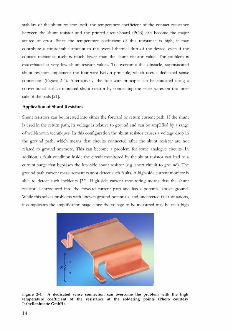
14
stability of the shunt resistor itself, the temperature coefficient of the contact resistance
between the shunt resistor and the printed-circuit-board (PCB) can become the major
source of error. Since the temperature coefficient of this resistance is high, it may
contribute a considerable amount to the overall thermal drift of the device, even if the
contact resistance itself is much lower than the shunt resistor value. The problem is
exacerbated at very low shunt resistor values. To overcome this obstacle, sophisticated
shunt resistors implement the four-wire Kelvin principle, which uses a dedicated sense
connection (Figure 2-4). Alternatively, the four-wire principle can be emulated using a
conventional surface-mounted shunt resistor by connecting the sense wires on the inner
side of the pads [21].
Application of Shunt Resistors
Shunt resistors can be inserted into either the forward or return current path. If the shunt
is used in the return path, its voltage is relative to ground and can be amplified by a range
of well-known techniques. In this configuration the shunt resistor causes a voltage drop in
the ground path, which means that circuits connected after the shunt resistor are not
related to ground anymore. This can become a problem for some analogue circuits. In
addition, a fault condition inside the circuit monitored by the shunt resistor can lead to a
current surge that bypasses the low-side shunt resistor (e.g. short circuit to ground). The
ground path current measurement cannot detect such faults. A high-side current monitor is
able to detect such incidents [22]. High-side current monitoring means that the shunt
resistor is introduced into the forward current path and has a potential above ground.
While this solves problems with uneven ground potentials, and undetected fault situations,
it complicates the amplification stage since the voltage to be measured may be on a high
Figure 2-4: A dedicated sense connection can overcome the problem with the high temperature coefficient of the resistance at the soldering points (Photo courtesy Isabellenhuette GmbH).
15
voltage potential. If this voltage potential is of practical amplitude, an integrated high-side
current monitor or differential amplifier can be employed. Many semiconductor companies
have high-side current monitors in their portfolios with some of them able to work with
common-mode voltages from -16 V up to 80 V with a bandwidth of around 1 MHz at a
gain of 100.
High performance coaxial shunt resistors are used to measure high impulse currents in
specialized applications such as exploding wire circuits, nuclear fusion and lightning studies.
Surface mounted devices, on the other hand, are employed in power converter systems,
industrial applications, mobile devices and consumer electronics.
2.2.2 Printed-Circuit-Board Trace Resistance Sensing
Instead of using a dedicated shunt resistor, it is possible to use the intrinsic resistance of a
conducting element in the circuit (usually a copper trace or busbar). This approach
promises very low cost with no additional power losses. Naturally, the resistance of a
copper trace is very low, and thus the resulting voltage drop very small [23]. To get a useful
output signal, an amplifier with high gain is required. The limited gain-bandwidth-product
of the amplifier will then alter the performance of this current sensing method.
Spaziani [23] provided design equations and recommendations for a PCB copper shunt
resistor. However, he concluded that this approach is not suitable for applications requiring
reasonable accuracy due to the large thermal drift. A technique to compensate for this
thermal drift that works without temperature sensing has been proposed especially for
power converter applications, in which the input current of the converter is used to track
the thermal drift of the copper trace [24]. This technique is limited to power converter
applications, and does not work properly below 20% of the rated nominal current range. It
should also be noted that it is impossible to control the resistance of a copper trace or
busbar with satisfactory precision during production process. So, in order to get a sensor
signal with reasonable accuracy at 25°C, it is necessary to calibrate the sensor signal, and
then combine the measurement of the voltage drop with the correction for the temperature
of the busbar.
Since only a very limited number of publications are available on this method, it seems that
this technique is only used in niche applications. However, due to the high cost pressure in
the power conversion industry, this method may become more popular as a replacement
for shunt resistors in order to reduce power losses and to increase power density.

16
2.2.3 MOSFET Sensing
Exploiting the On-Resistance of the MOSFET
Another conduction element present in many electrical circuits is a MOSFET, which has a
fairly linear resistance RDSon during on-state [21]. MOSFETs are usually employed in power
conversion stages, and thus are an alternative to the copper trace sensing approach. An
advantage over the copper trace approach is the higher resistance, which yields a larger
voltage drop.
An exemplary application in the buck converter topology with synchronous rectification is
shown in Figure 2-5 [4]. Here, the aim is to measure the current through the inductor L in
order to enable current sharing, monitoring and limiting. The two switches Q1 and Q2 are
controlled alternately, which means that during the first time interval (Q1 = on, Q2 = off)
the inductor current flows through Q1, and during the second time interval through Q2.
Accordingly, the inductor current can be determined based on the current information of
either Q1 or Q2. Normally the voltage drop vs across Q2 is used since Q2 relates to ground
potential, and thus allows a simple measurement.
Due to tolerances in the MOSFET manufacturing process, the parameter RDSon is subject to
large device-to-device variation that makes a calibration necessary. RDSon also exhibits a
significant thermal drift that has to be corrected. One proposed solution is to carry out
frequent reference measurements to calibrate the on-resistance RDSon of the MOSFET and
to track its thermal drift [25]. This method involves an additional MOSFET parallel to Q2
with a precision shunt resistor connected in series. It is then feasible to drive the gate of
this MOSFET, e.g. once every thousand switching cycles instead of Q2, to obtain a more
precise current measurement from the shunt resistor voltage that is used to calibrate the
L
C R
Controller
vout
+
-
Q2
Q1
+
-
vin
vs
i(Q2)
i(Q1)
i(L)
+
-
Figure 2-5: The voltage drop across the MOSFET Q2 that is connected to ground can be used to measure currents. The strong thermal drift of RDSon and its unit-to-unit variation limit the practicality of this principle.

17
RDSon value. This method corrects for initial tolerance and thermal drift of RDSon at small
additional power loss. However, the circuit complexity and cost is increased.
Quite often amplification of the voltage drop across the MOSFET will be necessary
because the MOSFET will be chosen in order to minimise power loss and to maximise
efficiency, so that the voltage drop across RDSon is typically small. One also has to be aware
that the parasitic inductance of RDSon is given by the mutual inductance built by the sense
loop as described above for the shunt resistor. Since MOSFETs are usually not optimised
for this application, the resulting parasitic inductance may be large and results in decreased
dynamic performance at higher frequency.
Sense FET Technique
Another MOSFET related current sensing method is illustrated in Figure 2-6. A power
MOSFET normally consists of n parallel-connected small MOSFET cells that share the
same drain, source and gate terminal. Since all MOSFET cells see the same drain to source
voltage, the total drain current is equally shared between them. It is now possible to
connect the source connection of one single MOSFET cell to another terminal called sense
terminal to make it accessible outside the MOSFET package. Accordingly, the current IC
through this sense connection is:
,n
II D
C = (2-4)
while ID is the total MOSFET drain current. With this technique, it is possible to obtain a
current sample more precise than 3% [21]. The result is called sense FET and can be
employed as an alternative to the on-resistance current sensing technique depicted in
Figure 2-5.
However, this equation is only valid if the drain to source voltage of the single MOSFET
cell is the same as all the other cells. Therefore a Kelvin connection is typically available
that provides the internal source voltage potential to eliminate problems with resistive
voltage drops across the source connection. In Figure 2-6 an active amplifier circuit is
shown that actively keeps the voltage difference between sense and Kelvin terminal at zero,
and provides an output voltage proportional to the sense current. This configuration allows
good accuracy but relies on expensive high-bandwidth amplification to provide good
dynamic performance.
For low-cost current sensing with low accuracy requirements, it is feasible to connect a
sense resistor Rs between the source and Kelvin terminal. However, due to the voltage
difference between sense and Kelvin terminal, the current sample IC is altered to (n >> 1):
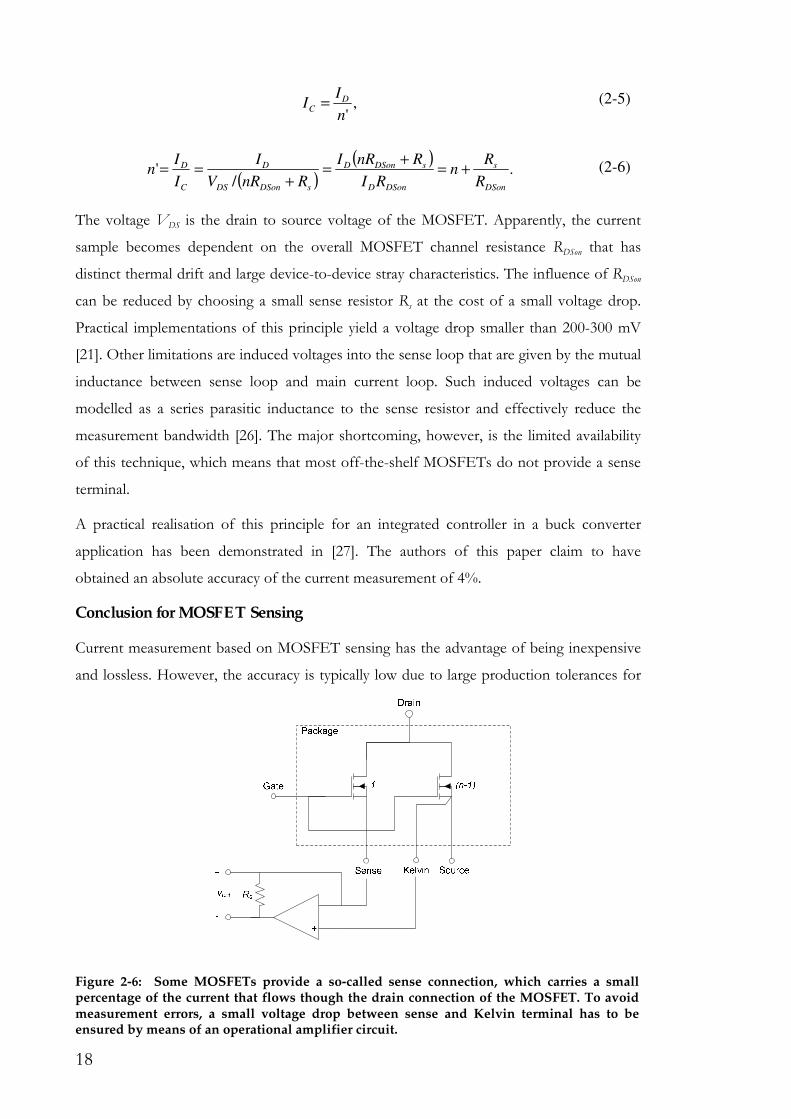
18
,'n
II D
C = (2-5)
( )( )
./
'DSon
s
DSonD
sDSonD
sDSonDS
D
C
D
R
Rn
RI
RnRI
RnRV
I
I
In +=
+=
+== (2-6)
The voltage VDS is the drain to source voltage of the MOSFET. Apparently, the current
sample becomes dependent on the overall MOSFET channel resistance RDSon that has
distinct thermal drift and large device-to-device stray characteristics. The influence of RDSon
can be reduced by choosing a small sense resistor Rs at the cost of a small voltage drop.
Practical implementations of this principle yield a voltage drop smaller than 200-300 mV
[21]. Other limitations are induced voltages into the sense loop that are given by the mutual
inductance between sense loop and main current loop. Such induced voltages can be
modelled as a series parasitic inductance to the sense resistor and effectively reduce the
measurement bandwidth [26]. The major shortcoming, however, is the limited availability
of this technique, which means that most off-the-shelf MOSFETs do not provide a sense
terminal.
A practical realisation of this principle for an integrated controller in a buck converter
application has been demonstrated in [27]. The authors of this paper claim to have
obtained an absolute accuracy of the current measurement of 4%.
Conclusion for MOSFET Sensing
Current measurement based on MOSFET sensing has the advantage of being inexpensive
and lossless. However, the accuracy is typically low due to large production tolerances for
Figure 2-6: Some MOSFETs provide a so-called sense connection, which carries a small percentage of the current that flows though the drain connection of the MOSFET. To avoid measurement errors, a small voltage drop between sense and Kelvin terminal has to be ensured by means of an operational amplifier circuit.
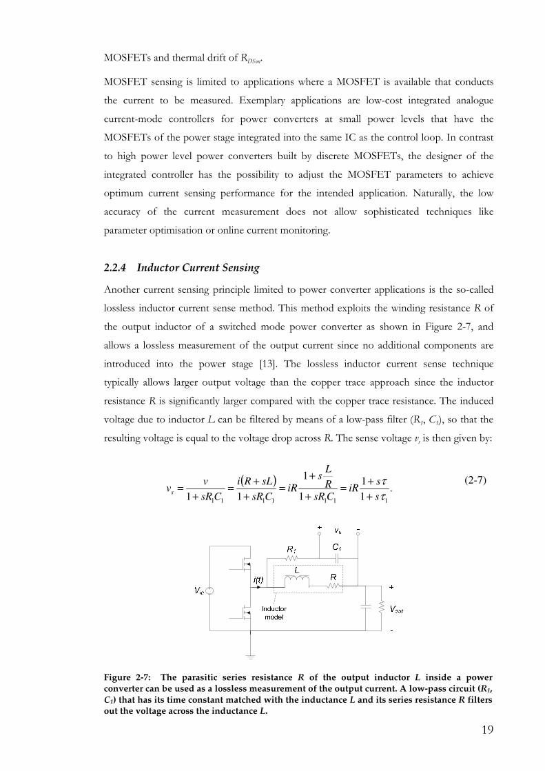
19
MOSFETs and thermal drift of RDSon.
MOSFET sensing is limited to applications where a MOSFET is available that conducts
the current to be measured. Exemplary applications are low-cost integrated analogue
current-mode controllers for power converters at small power levels that have the
MOSFETs of the power stage integrated into the same IC as the control loop. In contrast
to high power level power converters built by discrete MOSFETs, the designer of the
integrated controller has the possibility to adjust the MOSFET parameters to achieve
optimum current sensing performance for the intended application. Naturally, the low
accuracy of the current measurement does not allow sophisticated techniques like
parameter optimisation or online current monitoring.
2.2.4 Inductor Current Sensing
Another current sensing principle limited to power converter applications is the so-called
lossless inductor current sense method. This method exploits the winding resistance R of
the output inductor of a switched mode power converter as shown in Figure 2-7, and
allows a lossless measurement of the output current since no additional components are
introduced into the power stage [13]. The lossless inductor current sense technique
typically allows larger output voltage than the copper trace approach since the inductor
resistance R is significantly larger compared with the copper trace resistance. The induced
voltage due to inductor L can be filtered by means of a low-pass filter (R1, C1), so that the
resulting voltage is equal to the voltage drop across R. The sense voltage vs is then given by:
( ).
1
1
1
1
11 1111111 τ
τ
s
siR
CsRR
Ls
iRCsR
sLRi
CsR
vvs
+
+=
+
+=
+
+=
+=
(2-7)
Figure 2-7: The parasitic series resistance R of the output inductor L inside a power converter can be used as a lossless measurement of the output current. A low-pass circuit (R1, C1) that has its time constant matched with the inductance L and its series resistance R filters out the voltage across the inductance L.

20
Matching the time constants of τ1 and τ yields [13]:
.iRvs = (2-8)
The method described in [28] uses the same underlying principle but has the sense wires
differently connected, so that the measured voltage is vs = iR + v0.
While in the first place this solution appears to be straightforward, problems arise due to
thermal drift of R, R1, C1 and inductance L. In addition, the value of L depends on the DC
offset current flowing through the inductor due to variations in the permeability of the core
as a function of core magnetization, and large initial tolerances of R, R1, C1 and L make a
calibration necessary. Forghani-zadeh et al. reported an accuracy of ±4% for DC currents
by using a calibration procedure before start-up in order to determine the values of L and
R [29].
In conclusion, the inductor current sense method is another low-cost solution for current
sensing in power converters with low accuracy. The measurement accuracy is limited by
several component tolerances that as a whole are difficult to compensate.
2.2.5 Conclusion for Current Sensor Based on Ohm’s law of Resistance
Ohm’s law of resistance provides the simplest way to measure currents. A significant
drawback of this kind of current sensor is the unavoidable electrical connection between
the current to be measured and the sense circuit. By employing a so-called isolation
amplifier, electrical isolation can be added. However, isolation amplifiers are expensive. As
an example, an integrated circuit (AD202) comes at an approximate price of around 30
USD at 1k volume. They also deteriorate the bandwidth, accuracy, and thermal drift of the
original current sensing method. For these reasons, current sensing techniques based on
physical principles that provide inherent electrical isolation normally provide better
performance at lower cost in applications where isolation is required.
2.3 Current Sensors that Exploit Faraday’s Law of Induction
Current sensors based on Faraday’s law of induction are one example of sensors that
provide inherent electrical isolation between the current one wants to measure and the
output signal. Electrical isolation enables the measurement of currents on a high and
floating voltage potential by providing a ground-related output signal. In many applications
safety standards demand electrical isolation, and thus make isolated current sensing
techniques mandatory.

21
2.3.1 Rogowski Coil
The Rogowski coil displayed in Figure 2-8 is a classical example of an application based on
Faraday’s law of induction. The working principle can be explained starting with amperes
law that defines the path integral of the magnetic flux density B inside the coil:
.0 C
C
ildB µ=⋅∫rr
(2-9)
The current iC flows through the area enclosed by curve C. To allow a simple theoretical
analysis, it is assumed that the cross section diameter of the Rogowski coil is much smaller
than its radius r. This assumption is valid for most coil designs. If the current iC is centred
inside the coil, the magnetic flux density B can be simplified to:
.2 r
iB Co
π
µ= (2-10)
One can apply Faraday’s law of induction to determine the induced voltage into the
Rogowski coil due to a change in the current iC:
.2
0
dt
di
r
NA
dt
dBNA
dt
dNv C
π
µφ−=−=−= (2-11)
A is the cross sectional area of the coil body which is formed by the windings, and N the
number of turns. Voltage v is proportional to the derivative of the primary current iC that
has to be measured. An integrator with integrating constant k, and infinitely high input
impedance can yield the exact result:
).0(2
)0(2
00outCout
t
Cout vi
r
NAkvdt
dt
dik
r
NAv +−=+⋅−= ∫ π
µ
π
µ (2-12)
Equation (2-12) is also theoretically valid if the coil is not centred around the conductor or
the coil shape is not circular [30]. By having a look into the datasheet of a commercial
Rogowski coil, however, one finds that the typical measurement error is increased if the
∫
Figure 2-8: Schematic of a Rogowski coil that uses a nonmagnetic core material. An integrator is required to get a signal proportional to the primary current ic from the induced voltage.

22
coil is not centred as shown in Figure 2-9 [31]. This is due to the fact that in reality the
winding density around the coil is never perfectly constant. Accordingly, the poorest
accuracy is obtained if the conductor position is close to the clip together mechanism,
where the winding density cannot be even.
Although (2-12) implies that the Rogowski coil can also measure direct currents, one has to
keep in mind that the basic principle is based on the detection of a flux change, which is
proportional to a current change. Without knowing what the current was at t = 0, which is
represented by vout(0) in (2-12), it is impossible to reconstruct the DC component. Since
practical integrators are not perfect and may exhibit a small but steady input offset voltage,
its frequency response has to be altered, so that the gain at low frequency is reduced.
Hence, practical Rogowski coils are not suitable to measure low-frequency currents (Figure
2-10) [30, 32, 33]. For this reason, it has been recently proposed to combine the Rogowski
coil with an open-loop magnetic field sensor that provides the DC information to extend
the measurement range to direct currents [34].
While active integrators allow almost freely adjustable integrator gains k, they limit the
maximum rise time and exhibit saturation at high output voltages. The rise time
performance can be improved by using passive integration at the cost of lower gain k. For
highest performance, a Rogowski coil with current output has been proposed that exploits
its self-inductance for passive integration [32]. Other research has focused on integrating
the Rogowski coil into a PCB in order to reduce its bulk [35].
The sensitivity of the Rogowski coil is small compared to a current transformer, because
the current transformer can take advantage of the high permeability of the magnetic core
material. This can be compensated for by adding more windings on the Rogowski coil or
using a higher integrator gain k. However, more windings increase the self-capacitance and
self-inductance, whereas a higher integrator gain requires an amplifier with large gain-
bandwidth product.
Conductor Position Typical Error
< 1%
< 0.2%
< 3%
Figure 2-9: The influenced of the conductor position on the accuracy of the Rogowski coil.

23
The Rogowski coils thermal drift is determined by the integrator but also by the fact that
due to the thermal expansion of the coil the cross sectional area A of the coil body may
change. Vibrations can lead to a similar effect because of sliding turns on the coil. Dupraz
et al. mitigated these problems by integrating the coil windings into a PCB [36].
Rigid coils usually have a higher sensitivity since they allow more turns than flexible coils,
and thus provide a lower cut-off frequency as illustrated in Figure 2-10. On the downside,
they do not provide the exceptional handling capability of flexible coils, and the large
number of turns deteriorates the high-frequency performance.
A distinct feature of the Rogowski coil is that it does not exhibit saturation, and is
inherently linear [30, 32]. This makes it especially useful in situations were the amplitude of
the current pulse is unknown. Rogowski coils can be applied to measure currents in power
distribution systems, short-circuit testing systems, electromagnetic launchers, slip-ring
induction motors and lightning test facilities. The cost is comparable with that of current
transformers but with the advantage of less insertion impedance and, in the case of flexible
coils, higher user-friendliness.
2.3.2 Current Transformer
Similar to the Rogowski coil, the current transformer (CT) also exploits Faraday’s law of
induction to measure currents. The construction is basically the same as the Rogowski coil,
with one single primary turn and multiple secondary turns but employs a core material with
high relative permeability (Figure 2-11). The main difference between a CT and a Rogowski
coil is that the secondary winding of the current transformer is loaded with a sense resistor
Rs. The current is through Rs generates a magnetic flux that acts to counter the flux
generated by the primary current. It is possible to modify (2-11) derived for the Rogowski
1.E-03
1.E-01
1.E+01
1.E+03
1.E+05
1.E+07
1.E-02 1.E+00 1.E+02 1.E+04 1.E+06
Frequency [Hz]
Cu
rre
nt
[A]
Rigid Coil Lower Limit
Flexible Coil Lower Limit
Flexible Coil Upper Limit
Rigid Coil Upper Limit
Figure 2-10: Current / Frequency limits of Rogowski coils. Rigid coils have the advantage of being able to measure at smaller frequencies, whereas flexible coils have improved handling capability, and usually can measure at higher frequencies.

24
coil as follows:
( ) ,0
dt
dNii
lNA
dt
dNv sc
m
rs −−=−=
µµφ (2-13)
where A is the cross sectional area of the core. This equation can be solved for is:
.0
2 ∫ ⋅−=t
s
r
mcs dtv
AN
l
N
ii
µµ (2-14)
The second term of (2-14) can be interpreted as an inductance and is commonly known as
the magnetizing inductance Lm:
.1∫ ⋅−=t
s
m
cs dtv
LN
ii (2-15)
Based on (2-15), one can construct the equivalent circuit diagram of a current transformer
using a theoretical DC transformer (Figure 2-12a). It has to be noted, that this equivalent
circuit is very basic and neglects stray inductances, core losses and winding resistance.
However, it can be easily justified with the above equations, and gives sufficient insight to
understand the current transformer working principle. The capacitor Cw has been added to
model the secondary winding capacitance. The importance of this capacitance will be
described below.
The second term in (2-15) also models the inability of the CT to measure direct currents. If
the primary current ic contains a DC component then the magnetizing current im will
increase until the full DC component flows through Lm (Figure 2-12a). So in the standard
configuration the current transformer is incapable of measuring DC currents. On the other
hand, if the second term in (2-15) is small, which is true when the frequency is relatively
high, then the secondary current is directly proportional to the primary current ic, and can
Figure 2-11: A current transformer consisting of one primary turn and multiple secondary turns so as to reduce the current flowing on the secondary side (Image courtesy Power-One Inc).
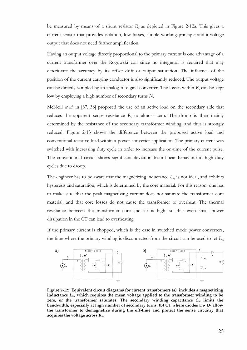
25
be measured by means of a shunt resistor Rs as depicted in Figure 2-12a. This gives a
current sensor that provides isolation, low losses, simple working principle and a voltage
output that does not need further amplification.
Having an output voltage directly proportional to the primary current is one advantage of a
current transformer over the Rogowski coil since no integrator is required that may
deteriorate the accuracy by its offset drift or output saturation. The influence of the
position of the current carrying conductor is also significantly reduced. The output voltage
can be directly sampled by an analog-to-digital-converter. The losses within Rs can be kept
low by employing a high number of secondary turns N.
McNeill et al. in [37, 38] proposed the use of an active load on the secondary side that
reduces the apparent sense resistance Rs to almost zero. The droop is then mainly
determined by the resistance of the secondary transformer winding, and thus is strongly
reduced. Figure 2-13 shows the difference between the proposed active load and
conventional resistive load within a power converter application. The primary current was
switched with increasing duty cycle in order to increase the on-time of the current pulse.
The conventional circuit shows significant deviation from linear behaviour at high duty
cycles due to droop.
The engineer has to be aware that the magnetizing inductance Lm is not ideal, and exhibits
hysteresis and saturation, which is determined by the core material. For this reason, one has
to make sure that the peak magnetizing current does not saturate the transformer core
material, and that core losses do not cause the transformer to overheat. The thermal
resistance between the transformer core and air is high, so that even small power
dissipation in the CT can lead to overheating.
If the primary current is chopped, which is the case in switched mode power converters,
the time where the primary winding is disconnected from the circuit can be used to let Lm
Figure 2-12: Equivalent circuit diagrams for current transformers (a) includes a magnetizing inductance Lm, which requires the mean voltage applied to the transformer winding to be zero, or the transformer saturates. The secondary winding capacitance Cw limits the bandwidth, especially at high number of secondary turns. (b) CT where diodes D1- D3 allow the transformer to demagnetize during the off-time and protect the sense circuitry that acquires the voltage across Rs.

26
demagnetize itself through diodes D2 and D3 with a circuit shown in Figure 2-12b. This
avoids saturation of the magnetizing inductance Lm and allows it to measure direct currents
[21]. Using this principle it is possible to measure the output current of a power converter
by sensing the current through the MOSFET’s with a current transformer [39]. Diode D1
in Figure 2-12b protects the measurement circuitry connected to the sense resistor from
the negative voltage, which appears at the secondary winding during the demagnetization
process. Since the mean voltage across the magnetizing inductance has to be zero,
sufficient time needs to be available to reset the core magnetization. This has implications
on the maximum allowed duty cycle of the switched mode power converter. Principally the
zener voltage of diode D3 can be adjusted in order to reduce the demagnetization time. In
practice, however, the secondary winding capacitance Cw limits the rise time of the voltage
across the secondary transformer winding. The technique of McNeill et al. mentioned
above is useful here as well since it substantially reduces the reverse voltage that has to be
applied to demagnetize the transformer core. This improvement comes at higher cost, and
the bandwidth of the current sensor becomes dependent on the performance of the active
load.
Despite the described shortcomings, current transformers are very popular in power
conversion applications because of their low cost, and the ability to provide an output
signal that is directly compatible with an analogue-to-digital converter. They are also
intensively employed in power distribution networks at 50/60 Hz line frequency.
2.4 Current Sensing by Means of Magnetic Field Sensors
In the previous section current sensors that exploit Faraday’s law of induction have been
discussed. Due to the nature of this law it is impossible to sense currents that generate
0
20
40
60
80
100
120
5 15 25 35 45 55 65 75 85 95
Duty Cycle (%)
vout (mV)
vout
(ideal)
vout
(modified circuit)
vout
(conventional
diode-resistor circuit)
0
20
40
60
80
100
120
5 15 25 35 45 55 65 75 85 95
Duty Cycle (%)
vout (mV)
vout
(ideal)
vout
(modified circuit)
vout
(conventional
diode-resistor circuit)
Figure 2-13: Output voltage vs. duty cycle for a CT. Due to the droop effect, the linearity of the current transformer is degraded at high duty cycle or current pulse with large on-times (vout is the low-pass filtered sense voltage vs). The method proposed by McNeill et al. reduces the excursion of the flux within the magnetizing inductance, and thus leads to a superior linearity [37].

27
static magnetic fields. Magnetic field sensors, on the other hand, are able to sense static and
dynamic magnetic fields. For this reason they provide an attractive alternative basis for
sensing currents. This section first explains the different sensing configurations. Three
different configurations are normally used to build a current sensor based upon magnetic
field sensing devices. These are open-loop, closed-loop and a third method that combines
magnetic field sensor either with a current transformer or Rogowski coil. After the
explanation of the available sensing configuration, the most popular magnetic field sensing
technologies are explained.
2.4.1 Sensing Configurations
Open-Loop Technology
The open loop configuration provides a simple method to use a magnetic field sensor for
current sensing. Figure 2-14 shows the basic principle, where a magnetic field sensor that
may be integrated into a SMD IC (integrated-circuit) is placed in close vicinity to the
current carrying conductor. This principle has the advantage of being simple, inexpensive
and compact. It assumes that the magnetic field around the conductor at a certain distance
is proportional to the current at all times. The sensitivity, linearity and thermal drift are
generally determined by the magnetic field sensing principle.
There are several disadvantages to the open loop technique. Firstly in order to achieve high
precision in-situ calibration is required to determine the factor of proportionality between
magnetic field and current. The measurement bandwidth is not necessarily limited by the
sensing technology but by the required level of amplification of the output voltage. If the
sensor is located close to the current carrying conductor, the measurement accuracy may be
further reduced by the skin effect, which forces high frequency current to flow along the
outer edges of the conductor, and thus changes the magnetic field at the sensor. The most
serious limitation, however, is the susceptibility to stray external magnetic fields. These
Figure 2-14: The simplest schematic for open-loop current measurement. It uses a magnetic field sensor that directly measures the magnetic field around the current carrying conductor. External magnetic fields significantly deteriorate the accuracy of this technique.

28
fields can significantly disturb the measurement accuracy. As an example, permanent
magnets and inductors can easily disturb the output signal by several percent even if they
are separated by more than 10 centimetres from the field sensor. It is possible to shield
against these fields but shielding is complicated, needing to shield against both static and
dynamic fields. These shields employ materials with high conductivity and high
permeability. Moreover, the presence of a magnetic shield will also change the magnetic
field at the sensor’s position, exhibit losses due to eddy currents, and change its
permeability based on the offset magnetization and frequency. All this makes it very
complicated to obtain a linear and reproducible relation between the current and measured
magnetic field over a wide frequency range.
A slightly more complex sensor is based upon a magnetic core that is placed around the
conductor to concentrate the magnetic field from the primary current ic onto the magnetic
field sensing device (Figure 2-15). This significantly reduces the influence of external
magnetic fields, increases the sensitivity thanks to the high relative permeability of the core
and eliminates the need for in-situ calibration in order to determine the constant of
proportionality between the current and magnetic field. Moreover, the skin effect within
the conductor has no influence on the current sensing accuracy.
The performance of this kind of current sensor is not only determined by the type of
magnetic field detection but also by the properties of the magnetic core material. Core
losses usually limit the measurement bandwidth of this sensing principle below the
capabilities of the magnetic field sensing device. The losses are a combination of hysteresis
and eddy current losses, and can lead to excessive heating. Many commercial available
transducer based on this principle require a down rating of high frequency currents in order
to avoid overheating. In addition, an excessive overcurrent situation can saturate the
magnetic core material causing a change in the operating point of this sensor. This effect is
known as magnetic offset, and causes a constant offset voltage on the output signal. This
Figure 2-15: Schematic for an open-loop current sensing configuration using a magnetic core to concentrates the field from the primary conductor onto the magnetic sensor. This not only increases the sensitivity of the current sensor due to the permeability of the core material but decreases the sensitivity to external magnetic fields.

29
offset voltage can lead to an absolute error higher than 1% and is permanent. It is possible
to retrieve the initial operating point by degaussing the core. This involves driving the core
from negative to positive magnetization in decreasing amplitude, illustrated in Figure 2-16
[40]. The fringing field around the core gap may also induce a parasitic voltage into the
measurement electronics.
Closed-Loop Technology
In a closed-loop configuration, the output voltage of the magnetic field sensor is used as an
error signal to compensate the magnetization inside the magnetic core by forcing a current
is through a second transformer winding. This current generates a magnetic field that
opposes the primary current ic as illustrated in Figure 2-17. Assuming the current is perfectly
compensates the magnetic flux, is is proportional to the primary current ic. This technique
greatly reduces the influence of the thermal drift of the magnetic field sensing device. The
linearity also becomes independent of the magnetic field sensor, and is therefore a
significant improvement over the open-loop technique. There will still be some offset
voltage present due to the amplification stage and the remanence of the core material that
may cause some temperature dependent drift. Excessive overcurrent can also change the
offset voltage of this measurement principle, and has to be removed by a degaussing cycle.
At high frequencies, the secondary winding can act as a current transformer to increase the
measurement bandwidth. Figure 2-18 demonstrates how the measurement electronic can
combine the output signals of the two operation principles to provide an output signal with
high bandwidth [40]. At the intersection of these two working principles the frequency
response is deteriorated by around 1 dB.
Another benefit of the closed loop sensor is that because the core magnetization is
theoretically zero there are no eddy current or hysteresis losses. In reality, a small core
magnetization will occur leading to some core losses but they will be significantly reduced
-1
0
1
0 35
Dem
ag
neti
zati
on
Cu
rren
t
> 5 cycles
> 30 cycles
Figure 2-16: A degaussing cycle, which consist out of a sinusoidal decreasing demagnetization current, is used to retrieve the initial operation point of the magnetic core material after an overcurrent incident.
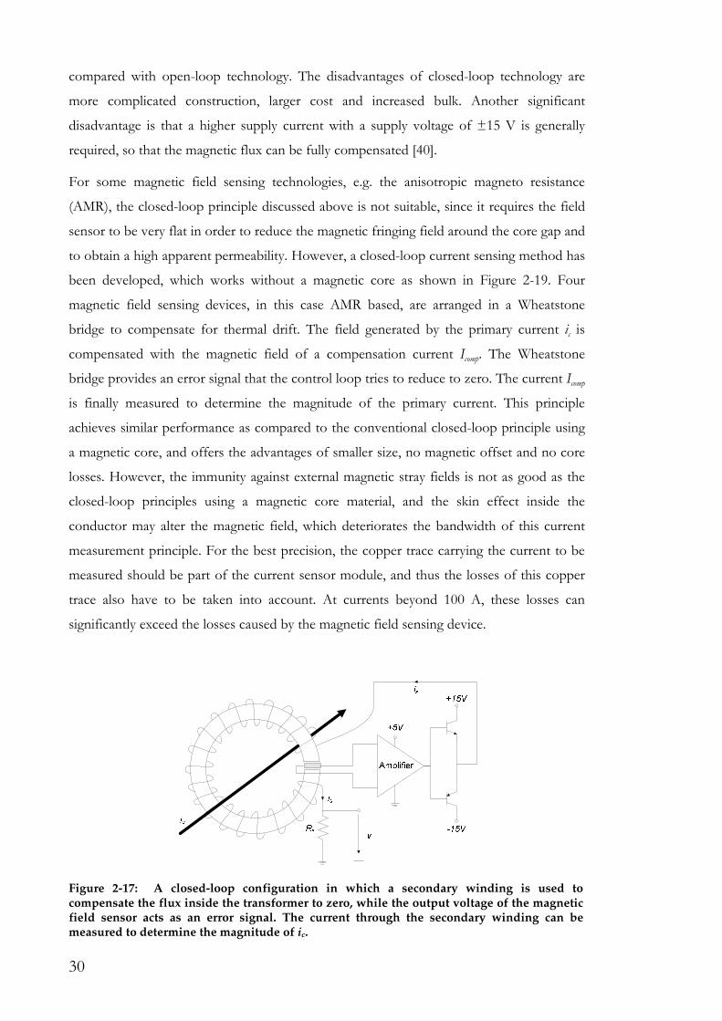
30
compared with open-loop technology. The disadvantages of closed-loop technology are
more complicated construction, larger cost and increased bulk. Another significant
disadvantage is that a higher supply current with a supply voltage of ±15 V is generally
required, so that the magnetic flux can be fully compensated [40].
For some magnetic field sensing technologies, e.g. the anisotropic magneto resistance
(AMR), the closed-loop principle discussed above is not suitable, since it requires the field
sensor to be very flat in order to reduce the magnetic fringing field around the core gap and
to obtain a high apparent permeability. However, a closed-loop current sensing method has
been developed, which works without a magnetic core as shown in Figure 2-19. Four
magnetic field sensing devices, in this case AMR based, are arranged in a Wheatstone
bridge to compensate for thermal drift. The field generated by the primary current ic is
compensated with the magnetic field of a compensation current Icomp. The Wheatstone
bridge provides an error signal that the control loop tries to reduce to zero. The current Icomp
is finally measured to determine the magnitude of the primary current. This principle
achieves similar performance as compared to the conventional closed-loop principle using
a magnetic core, and offers the advantages of smaller size, no magnetic offset and no core
losses. However, the immunity against external magnetic stray fields is not as good as the
closed-loop principles using a magnetic core material, and the skin effect inside the
conductor may alter the magnetic field, which deteriorates the bandwidth of this current
measurement principle. For the best precision, the copper trace carrying the current to be
measured should be part of the current sensor module, and thus the losses of this copper
trace also have to be taken into account. At currents beyond 100 A, these losses can
significantly exceed the losses caused by the magnetic field sensing device.
Figure 2-17: A closed-loop configuration in which a secondary winding is used to compensate the flux inside the transformer to zero, while the output voltage of the magnetic field sensor acts as an error signal. The current through the secondary winding can be measured to determine the magnitude of ic.
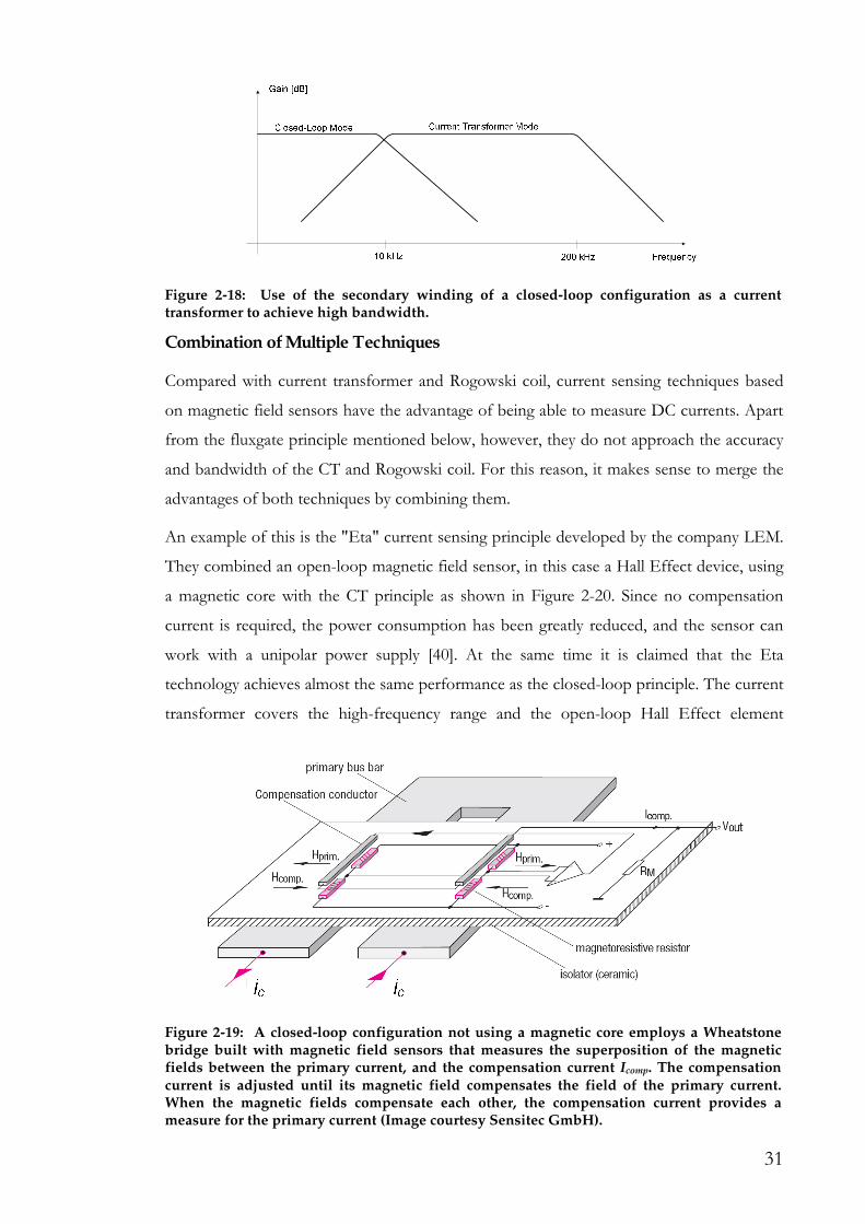
31
Combination of Multiple Techniques
Compared with current transformer and Rogowski coil, current sensing techniques based
on magnetic field sensors have the advantage of being able to measure DC currents. Apart
from the fluxgate principle mentioned below, however, they do not approach the accuracy
and bandwidth of the CT and Rogowski coil. For this reason, it makes sense to merge the
advantages of both techniques by combining them.
An example of this is the "Eta" current sensing principle developed by the company LEM.
They combined an open-loop magnetic field sensor, in this case a Hall Effect device, using
a magnetic core with the CT principle as shown in Figure 2-20. Since no compensation
current is required, the power consumption has been greatly reduced, and the sensor can
work with a unipolar power supply [40]. At the same time it is claimed that the Eta
technology achieves almost the same performance as the closed-loop principle. The current
transformer covers the high-frequency range and the open-loop Hall Effect element
Figure 2-18: Use of the secondary winding of a closed-loop configuration as a current transformer to achieve high bandwidth.
Figure 2-19: A closed-loop configuration not using a magnetic core employs a Wheatstone bridge built with magnetic field sensors that measures the superposition of the magnetic fields between the primary current, and the compensation current Icomp. The compensation current is adjusted until its magnetic field compensates the field of the primary current. When the magnetic fields compensate each other, the compensation current provides a measure for the primary current (Image courtesy Sensitec GmbH).

32
provides the low-frequency current information. In general the Eta technology based
current transducers are as expensive as closed loop Hall Effect current transducers.
The combination of magnetic field sensor and CT has been pushed further to build so-
called active current probes. These current sensors achieve a measurement bandwidth up
to 100 MHz and accuracy around 2% [20]. A planar sensor based on a combination
between CT and open-loop Hall Effect technology has been described by Dalessandro et al.
in [41] and Poulichet et al. in [42]. Other designs use a Rogowski coil to measure the high-
frequency part of the current [34]. Active current probes are complex in design, large in
size and fairly expensive. Therefore, they are typically used in measurement equipment, and
are not suitable for mass production. It should be noted that these combination techniques,
if they use a magnetic core, will need to degauss the core if a high overcurrent situation
occurs.
2.4.2 Magnetic Field Sensors
Hall Effect Sensor
One of the most popular magnetic field sensors is the Hall Effect sensor. This sensor is
based on the Hall Effect, which was discovered by Edwin Hall in 1879. He found that
when a current I flows through a thin sheet of conductive material that is penetrated by a
magnetic flux density B, a voltage v is generated perpendicular to both the current and field
(Figure 2-21):
,nqd
IBv = (2-16)
where q is the charge of the current carrier, n the carrier density and d the thickness of the
Figure 2-20: A schematic of the Eta technology, which combines the output of an open-loop Hall-effect sensor and a current transformer to achieve a high bandwidth current transducer. This greatly reduces the power consumption and enables the use of a 5 V supply voltage compared with ±15 V for closed-loop sensors.

33
sheet. It is interesting to note that the Hall Effect can be explained with the second term in
(2-1) that is neglected in Ohm’s law of resistance. This equation is valid for materials in
which the electrical conductivity is mediated by either positive or negative charge carriers.
This is the case for conductors, while for semiconductors a more complex coherence
exists. For this reason, the material properties are collected in the Hall coefficient RH [43]:
.1
nqRH = (2-17)
Indium antimonide (InSb), indium arsenide (InAs) and gallium arsenide (GaAs) are
examples of materials that are used in commercial Hall sensors [44]. Their typical
performance is depicted in TABLE 2-I [45]. The ohmic resistance is also an important
property, defining the power loss occurring inside the sensor due to the constant current I.
Hence, there is a trade-off between Hall plate thickness d, which determines the sensitivity,
and the Hall plate resistance.
Another problem related to the Hall Effect sensor can be seen within Figure 2-21: The
magnetic flux density B also penetrates the area enclosed by the sense wires. Accordingly, a
voltage is induced that makes it difficult to sense fast changing magnetic fields. This can be
solved by either routing the sense wire behind the Hall plate in order to minimize the active
area or by artificially creating an additional loop with the same area but opposite polarity,
so that the induced voltage cancels out [45].
At zero magnetic field, an offset voltage is present at the output, also known as
misalignment voltage. To use the Hall Effect as a current sensor, additional circuitry is
required, particularly to compensate for the misalignment voltage and the distinct thermal
drift [46]. Hall Effect sensors are found in open-loop, closed-loop, and combined
principles like Eta [40] and active current probes [42]. Advances in semiconductor
B
I +
-
v
Figure 2-21: Due to the Lorentz law, a flowing current I through a thin sheet of conductive material experiences a force if an external magnetic field B is applied. Therefore, at one edge of the sheet the density of conductive carrier is higher, resulting in a voltage potential v that is proportional to the magnetic field B.
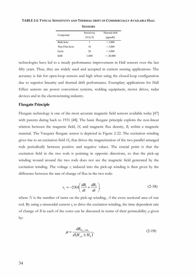
34
technologies have led to a steady performance improvement in Hall sensors over the last
fifty years. Thus, they are widely used and accepted in current sensing applications. The
accuracy is fair for open-loop sensors and high when using the closed-loop configuration
due to superior linearity and thermal drift performance. Exemplary applications for Hall
Effect sensors are power conversion systems, welding equipment, motor drives, radar
devices and in the electrowinning industry.
Fluxgate Principle
Fluxgate technology is one of the most accurate magnetic field sensors available today [47]
with patents dating back to 1931 [48]. The basic fluxgate principle exploits the non-linear
relation between the magnetic field, H, and magnetic flux density, B, within a magnetic
material. The Vacquier fluxgate sensor is depicted in Figure 2-22. The excitation winding
gives rise to an excitation field H0 that drives the magnetization of the two parallel arranged
rods periodically between positive and negative values. The crucial point is that the
excitation field in the two rods is pointing in opposite directions, so that the pick-up
winding wound around the two rods does not see the magnetic field generated by the
excitation winding. The voltage vs induced into the pick-up winding is then given by the
difference between the rate of change of flux in the two rods:
,2 21
+−=
dt
dB
dt
dBNAvs (2-18)
where N is the number of turns on the pick-up winding, A the cross sectional area of one
rod. By using a sinusoidal current i0 to drive the excitation winding, the time dependent rate
of change of B in each of the cores can be discussed in terms of their permeability µ given
by:
( ),
0
0
HHd
dB
ext
HHext
±=
±µ (2-19)
TABLE 2-I: TYPICAL SENSITIVITY AND THERMAL DRIFT OF COMMERCIALLY AVAILABLE HALL
SENSORS
Compound Sensitivity
[V/A·T]
Thermal drift
[ppm/K]
Bulk InAs 1 ≈ 3,000
Thin Film InAs 10 ≈ 3,000
GaAs 20 ≈ 3,000
InSb 1,600 ≈ -20,000

35
where µ is dependent on the field H = Hext ± H0 because of the non-linear behaviour of
the core (Figure 2-23a). The shape of the B-H loop given in Figure 2-23a is the
combination of the demagnetizing effects, associated with the geometry of the rods, and
the properties of the core material [49]. Combining (2-18) and (2-19) yields:
( ) ( ).2 0
20
1
−+
+−=
dt
HHd
dt
HHdNAv extext
s µµ (2-20)
For static external field Hext (2-20) becomes:
( ).2 210 µµ −−=
dt
dHNAvs
(2-21)
One can then define the differential permeability µd as:
( ) ( ).
0
2100
HHd
dB
HHd
dB
ext
HH
oext
HH
d−
−+
=−=−+
µµµ (2-22)
The differential permeability µd is time dependent due to the time dependent changes in the
excitation field H0 (Figure 2-23b). The voltage induced into the pick-up windings is then
given by:
.2 0
dt
dHNAv ds µ−= (2-23)
Provided that the external field (Hext) is small compared to the excitation field (H0), then
the peak in vs is proportional to external field and can be used to measure the field. Note
that in this analysis hysteresis has been neglected but can be modeled as a phase shift
between the excitation field, H0, and the differential permeability, µd.
The pick-up voltage vs is generally detected by measuring the second harmonic component.
As one can see in Figure 2-23b, the fundamental frequency of the pick-up voltage vs is
Figure 2-22: The Vacquier fluxgate principle: A sinusoidal current i0 periodically drives the core magnetization from positive to negative values, and thus changes the differential permeability seen by the external field Hext. The voltage vs induced into the pick-up winding is measured to determine the magnetic field Hext.

36
twice the frequency of the driving field H0. In closed-loop fluxgates, the pick-up voltage
serves as an error signal that generates an additional magnetic field that opposes Hext by
means of an additional winding or by driving the pick-up winding itself.
The sensitivity of the fluxgate method can be improved by using a higher excitation current
frequency, more turns on the pick-up winding, or a core with a rapidly changing
permeability µ, i.e. a core with rectangular B-H loop characteristic. However, tradeoffs have
to be made since a high excitation current frequency increases core losses, and the
distributed winding capacitance increases with N, and may lead to unwanted resonances
[50].
Numerous fluxgate principles other than the Vacquier are known, some of them process
the output signal in the time domain or have the excitation field orthogonal to the external
field H [48-51]. The second harmonic detection method, in general, provides the best
performance.
A fluxgate allows for some unique techniques to be used to measure currents that cannot
be realized using other field sensors. Some popular designs are depicted in Figure 2-24.
Firstly, the fluxgate based magnetic sensor can be used in a closed loop or open-loop
configuration as discussed above (Figure 2-24a). The magnetic field around the primary
current ic is concentrated by the magnetic core. In the closed-loop principle the secondary
winding is used to compensate the concentrated magnetic field. Due to the superior
sensitivity and temperature stability of the fluxgate method compared with other magnetic
field sensors, high accuracy is achieved.
In another technique a single closed annular magnetic core is used as shown in Figure
2-24b. In this embodiment, no pick-up winding is present, and the current through the
excitation winding is examined to determine the magnitude of the primary current ic [40,
52, 53]. In spite of the low-cost design, the thermal drift of this fluxgate current sensor is
Figure 2-23: The fluxgate method takes advantage of the fact that the permeability µ of a magnetic core material depends on the applied magnetic field.

37
still very low as demonstrated in Figure 2-25 using a 15 A current sensor based on the
sensing principle described in 5.3.2 (Amorphous core material, 100:1 turns ratio). On the
other hand, the bandwidth of this fluxgate configuration is limited by the time required to
drive the core between positive and negative saturation.
To increase the bandwidth, the fluxgate can be used together with a current transformer as
shown in Figure 2-24c. Here, the fluxgate principle provides the low-frequency current
information, while the current transformer is responsible for the high-frequency content.
Finally, Figure 2-24d illustrates the most advanced but also most costly adaptation that uses
a third core to compensate for the voltage noise introduced into the primary conductor by
the first fluxgate sensor. This voltage noise is in fact nothing else than the voltage applied
to the excitation winding multiplied by the turns ratio N, which is visible on the primary
side when the magnetic core material is not in saturation, thus acting as a transformer.
Many different current sensors with different names based on the fluxgate principle have
been proposed in literature [54-57]. These publications mainly deal with different variants
of evaluating the pick-up winding voltage to determine the current. Recently, an effort has
been made to integrate an open-loop fluxgate current sensor with PCB technology [58, 59].
Figure 2-24: The fluxgate principle can be used in different ways to measure currents. a) In a closed or open-loop configuration where the magnetic field sensor is represented by the fluxgate. b) Low frequency version using a closed toroid core without pick-up winding. c) Additional current transformer to extend the bandwidth. d) Having a third core to oppose the voltage disturbance introduced into the primary conductor by the first fluxgate.
-0.20
-0.15
-0.10
-0.05
0.00
25 45 65 85 105
Temperature [°C]
Ab
so
lute
Me
as
ure
me
nt
Err
or
[%]
-25 ppm/K
Figure 2-25: Thermal drift of a 15 A current sensor based on the fluxgate technology described in 5.3.2 (Amorphous core material, 100:1 turns ratio).

38
This is certainly a promising development towards low-cost applications. The achieved
linearity for the open-loop sensor was limited to 10% due to the difficulty of integrating
windings in PCB technology. Stand-alone fluxgate sensors are commercially successful but
so far only in high precision applications because of the high cost and size requirements.
Due to the very high accuracy, fluxgates are often employed in calibration systems,
diagnosis systems, laboratory equipment and medical systems.
Magneto Resistance Effect (MR)
It is possible to build structures in which the electrical resistance varies as a function of
applied magnetic field. These structures can be used as magnetic field sensors. The most
common application of these sensors has been as the read head in magnetic recording, but
they are now being examined for other potential applications. These resistors are normally
configured inside a bridge configuration to compensate for thermal drift. The two most
popular MR effects together with the most promising future candidates are discussed
below:
a) Anisotropic Magneto Resistance (AMR)
b) Giant Magneto Resistance (GMR)
c) Future candidates
a) Anisotropic Magneto Resistance (AMR) Sensors
The resistance of ferromagnetic materials, such as permalloy (an iron nickel alloy), is related
to the magnitude and direction of the applied magnetic field. In particular, a current I that
flows through a ferromagnetic material experiences a resistance that is dependent on the
angle between the current’s flow direction, and direction of magnetization M [60]. The
minimum resistance is when the magnetization M is perpendicular to the current I. The
resistance reaches its maximum when the current I flows parallel to the magnetization M.
In order to make the AMR effect sensitive to the direction of the magnetic field, the
current I is forced to flow at a 45° angle to the field direction via a series of aluminium bars
deposited onto a permalloy strip (Figure 2-26). This structure, known as barber poles,
provides a low impedance path for the current and directs it to flow at 45° to the initial
magnetization M0. The cost of this improvement is a reduction in the sensitivity of the
sensor due to a reduction in the change of the resistance.

39
Figure 2-27a shows the change in resistance ∆R/R in relation to the angle θ between the
material magnetization M and the current I. The maximum variation of this resistance is
very small, normally around 2-4% [47, 60, 61]. In Figure 2-27b a ferromagnetic strip is
shown together with the direction of current I and the magnetization M. The
magnetization M is the superposition between the initial magnetization direction, M0 and
the external applied magnetic field Hext. Due to the barber pole principle, the current I has a
45° offset towards the initial magnetization M0. If Hext is applied perpendicular to M0, the
resulting magnetization M changes its position. Hence, the angle between the current I and
magnetization M changes, and so does the permalloy strip’s resistance. Since the current is
forced to flow in a 45° angle to the initial magnetization M0, a bias is generated that allows
it to determine if the external field Hext is of positive or negative polarity (Figure 2-27a). By
using a constant current I, the voltage drop across the permalloy strip is now linear for a
certain range of negative and positive values for Hext, which is shown in Figure 2-28.
Moreover, the sensitivity can be adjusted by generating an artificial magnetic field Hx
parallel to the x-axis. For higher values of Hx the angle between the material magnetization
M and the current I will change less rapidly with Hext, which is also demonstrated in Figure
2-28.
The main problems of AMR sensors are high thermal drift, and high non-linearity. In
addition, a strong magnetic field can permanently change the intrinsic magnetization M0 of
the permalloy strip, and thus make the sensor useless until a reorientation of the
magnetization has been performed. The basic sensor principle has a thermal drift of 3000
ppm/K, which can be compensated by using the Wheatstone bridge configuration of
Figure 2-19. Hysteretic and eddy current effects inside the permalloy limit the frequency
response of the AMR technique to 1 MHz [60]. In commercial available AMR current
sensors, however, the limited gain-bandwidth product of the amplification stage normally
limits the frequency response to a few hundred kilohertz (Figure 2-29). AMR current
Figure 2-26: An AMR Sensor consisting of aluminum is vaporized onto a permalloy strip in a 45° angle against the intrinsic magnetization M0 so as to cause the current I to flow at 45° to M0 because of the much lower resistance of aluminum compared with permalloy.

40
sensors are available as open-loop magnetic field sensing devices or closed-loop current
sensors in the Wheatstone configuration depicted in Figure 2-19. The Wheatstone
configuration is currently somewhat more expensive than comparable closed-loop Hall
Effect current sensors. AMR current sensors are used in power conversion systems and
motor control applications.
b) Giant Magneto Resistance (GMR) Sensors
The GMR Effect is another technique used to detect static and dynamic magnetic fields. As
with the AMR Effect, the magnetic field has a direct influence on the apparent resistance R
of the GMR device. The discoverers Gruenberg and Fert received the 2007 Physics Nobel
Prize for this work [62, 63]. The importance of their work is justified by the fact that the
GMR Effect exhibits a change in resistance due to magnetic fields up to 12.8% at room
temperature compared with 2-4% for the AMR Effect [47]. This means that it is possible
Figure 2-27: The change in resistance of an AMR sensor as a function of the angle between the current I and the magnetization M. An external magnetic field Hext causes a change in the direction of M, which is the superposition between M0 and Hext.
Figure 2-28: The output voltage as a function of external magnetic field for an AMR sensor. By applying an auxiliary magnetic field Hx along initial direction of magnetization of the permalloy strip (M0) it is possible to adjust the field sensitivity of the sensor and suppress saturation effects.

41
to detect magnetic fields up to four times weaker than that measurable with the AMR
sensors. This ability has been used to improve the performance of read heads and so
increased the data density in hard disk drives. Using the GMR Effect it is now theoretically
possible to detect very small currents that were below the detection limit of sensors based
on AMR or Hall Effect. At the same time, the GMR technology is supposedly cheaper to
produce as the sensors are smaller and can be mass produced using standard
semiconductor technology.
The basic working principle of the GMR Effect can be explained using the spin-valve
structure [64]. It has to be noted that this is just one example of a structure that exhibits the
GMR Effect [47, 64]. The four-layer structure illustrated in Figure 2-30 is just a few tens of
nanometres thick and can be integrated into an IC. A thin conductor separates two
ferromagnetic layers. One ferromagnetic layer has its magnetization pinned by an
antiferromagnetic layer. The magnetization of the free magnetic layer is oriented by an
applied external field. If the free ferromagnetic layer is magnetized in the opposite direction
to the pinned layer, the resistance R perpendicular to the layers is large (Figure 2-30b). The
resistance is low when the external magnetic field orientates the magnetisation of the free
layer so that it is in the same direction as the pinned layer (Figure 2-30c). The reason for
the change in the apparent resistance R can be explained in terms of spin-dependent
electron scattering. In a simplified model it is distinguished between spin-up and spin-down
electrons. If the free and pinned ferromagnetic layers are pointing into the same direction,
only one type of electron is scattered significantly. If the two ferromagnetic layers point in
opposite directions, all electrons experience scattering, which results in an increase in the
apparent resistance R [65].
Although the GMR technology exhibits many desirable characteristics, there are serious
drawbacks that limit its usefulness in current sensing applications. The first problem is the
Figure 2-29: Frequency response of a commercial available AMR current sensor (Image courtesy Sensitec GmbH).

42
non-linear behaviour and distinct thermal drift. While for digital applications like the read
head of a hard drive the non-linearity is not a problem, a current sensor is supposed to be
linear, and thus a correction function needs to be employed. Additionally, a very strong
external field can unpin the pinned ferromagnetic layer and permanently alter the sensor
behaviour (Figure 2-30d).
At present, commercially available GMR current sensors work according to the core-less
open-loop principle (Figure 2-14). They are normally configured in a bridge configuration
in order to reduce thermal drift. As mentioned before, the skin effect inside the conductor
that carries the current to be measured may limit the bandwidth below the bandwidth
provided by the GMR sensor itself.
A prototype device has been simulated, designed and produced [66, 67]. The measurement
accuracy was found to be limited by the high thermal drift, with a temperature coefficient
beyond 1000 ppm/K and by the sensitivity to external magnetic fields. Another drawback
is that the GMR Effects exhibits notable hysteresis [68]. Figure 2-31 shows the measured
hysteresis of a GMR current sensor. Attempts have been made to remove the hysteresis by
using a sophisticated correction function that has been implemented in a digital-signal-
processor (DSP) [69].
Despite these problems, a lot of research is presently being carried out into GMR current
sensors. It seems that the potential cost advantage and gain in sensitivity against earlier
Antiferromagnet
Pinned (Hard) Ferromagnet
Free (Soft) Ferromagnet
Substrate
Thin
Conductor
Antiferromagnet
Pinned (Hard) Ferromagnet
Free (Soft) Ferromagnet
Substrate
Thin
Conductor
Antiferromagnet
Pinned (Hard) Ferromagnet
Free (Soft) Ferromagnet
Substrate
Thin
Conductor
Antiferromagnet
Pinned (Hard) Ferromagnet
Free (Soft) Ferromagnet
Substrate
Thin
Conductor
Hext
Hext
Hext = 0
Hext
(strong)
a)
b)
c)
d)
Figure 2-30: Basic working principle of the GMR Effect: a) At zero external magnetic field Hext, the resistance R(0) appears at the input leads. b) A magnetic field Hext that points into opposite direction as the intrinsic magnetization of the pinned ferromagnetic layer increases the resistance. c) The opposite happens if Hext points into the same direction as the pinned ferromagnetic layer’s magnetization. d) The intrinsic magnetization of the pinned ferromagnetic layer can be permanently changed by applying a strong external magnetic field Hext.
43
technologies like AMR and Hall Effect is significant. However, to date commercially
available core-less open-loop GMR sensors are still more expensive than comparable Hall
Effect and AMR devices. Their fields of application are similar to AMR and Hall Effect
based current sensors.
c) Future Candidates
In addition to existing field sensors there are a number of other field sensing technologies
that may be developed into future current sensors. One interesting candidate is the Giant
Magneto Impedance (GMI) effect. It has been observed that the impedance of amorphous
ribbon is a strong function of the applied magnetic field and the frequency of the
measurement current through the ribbon. At high driving frequencies, the impedance of
the amorphous ribbon is solely determined by the external applied field. To use the GMI
effect to sense magnetic fields, the ribbon can be included into an oscillator configuration
where its impedance influences the oscillator frequency [70-72]. The GMI effect is even
more sensitive to magnetic fields than the GMR effect.
Tunnelling Magneto Resistance (TMR) based on magnetic tunnel junctions is another
potential sensor technology that exhibits substantially higher field sensitivity than existing
AMR and GMR sensors. Using the TMR effect, resistance changes up to 230% at room
temperature have been reported [73, 74]. The structure and working principle is similar to
the GMR principle but uses a 1 nm thick insulator instead of a conductor to separate the
two ferromagnetic layers [47].
At this point there are no commercial current sensors based on these techniques available
but they have the potential to become more relevant in future due to the very high
Figure 2-31: An example of hysteresis effects within a GMR current sensor, which can be compensated by suitable algorithms within the interfacing electronics [55].

44
sensitivity.
2.4.3 Conclusion for Magnetic Field Sensors
Current transducers based on Hall Effect field sensors are widely used and accepted due to
their capability to measure direct currents whilst providing electrical isolation. The accuracy
is fair for open-loop sensors and high when using the closed loop technique. The most
serious limitation is the degaussing cycle required after an overcurrent incident, and the
distinct temperature related drift of the output voltage. Apart from the AMR sensor, the
other field sensing technologies are not employed yet in closed-loop principles. Therefore,
they suffer problems typical for open-loop sensors like fairly high thermal drift, poor
immunity against external fields and nonlinearity.
Applications for current sensor based on magnetic field sensing devices are far-reaching
and include power conversion systems, welding equipment, motor drives, radar devices and
electrowinning industry.
2.5 Current Sensors that Use the Faraday Effect
Light waves propagating through a medium exhibit a state of polarization that is given by
the electric field vector E as a function of time and location. In the most general case the
tip of the E field vector describes an ellipse. Circular polarization describes the special case
where the ellipse becomes a circle, whilst in linear polarization the ellipse collapses into a
line. The state of any polarization can always be described as the superposition of two
orthogonal linear or circular polarized light waves. A medium that changes the state of
polarization is said to be birefringent. Material having circular birefringence changes the
polarization of linear polarized light, and maintains the polarization of circular polarized
light. Linear birefringent material behaves vice versa [75]. One of Faraday's many
discoveries was that circular birefringence can be induced into a material by applying a
magnetic field parallel to the light propagation direction. If the intrinsic circular
birefringence of a medium is negligible small, the rotation plane of the polarization of
linear polarized light is proportional to the integral of applied magnetic field H along the
path s:
,∫ ⋅= sdHVrr
θ (2-24)
where the constant of proportionality V is the Verdet constant, a property of the medium
through which the light travels that describes the strength of the Faraday Effect. As
mentioned above, linear polarized light can be thought of as being composed of two

45
orthogonal circular polarized light waves. In particular, a linear polarized light wave is the
superposition of a right-hand circular polarized (RHCP) light wave orthogonal to a left-
hand circular polarized (LHCP) light wave. In the Faraday Effect the velocity of the RHCP
light waves is decreased if the magnetic field is pointing along its propagation direction, and
increased when the magnetic field points in the opposite direction. LHCP light waves
behave vice versa. This means that if linearly polarized light, which is the superposition of
RHCP and LHCP light, is fed into a material undergoing the Faraday Effect there will be a
phase difference induced between the two different circularly polarized beams, and as a
result the polarization plane of the linear polarized light is rotated.
Researchers have been investigating optical current transformers that exploit the Faraday
effect for more than three decades [76]. They provide an attractive alternative in
applications where excellent electrical isolation is essential, e.g. in power distribution
systems. In these applications the construction of traditional current transformers becomes
increasingly difficult and expensive due the requirements placed upon the insulation
material that needs to withstand very high voltages, and need to avoid saturating the core
material. As an additional benefit, optical current sensors also enable the measurement of
direct currents beyond 100 kA. A commercially available 500 kA DC fiber-optic current
sensor has been described in [77]. This sensor uses a negligible amount of energy and space
compared with existing Hall current sensors that dissipate several kilowatts of power, and
can weight more than two tons [78].
2.5.1 Polarimeter Detection Method
A straightforward way to use the Faraday Effect to measure current is depicted in Figure
2-32. Linear polarized light is feed into a fibre-optic coil with N turns that encloses the
current ic to be measured. The rotation θ of the linear polarized light can be calculated using
Ampere’s law:
( )θ2sin12
0 +=I
Id
0I
Figure 2-32: A schematic of a fibre polarimeter, which is the simplest technique used to measure the current, ic, using the Faraday technique.

46
.cVNi=θ (2-25)
A desirable effect of using a fibre-optic coil is that only magnetic fields due to currents
inside the coil are detected as external stray magnetic fields will in general cancel out.
Moreover, the position of the current carrying conductor within the fibre-optic coil has no
appreciable influence on the measurement accuracy. The analysing circuit consists of a
polarizer at 45° to the original polarization direction so that the output light intensity Id is
given by:
( ),2sin12
0 θ+=I
Id (2-26)
where I0 is the input light intensity. For small rotation θ, the sine function can be linearized.
A major problem with the configuration shown in Figure 2-32 is the dependence of the
output signal on the input light intensity I0. This problem can be addressed by using a
polarizing beam splitter (Wollaston prism) set at 45° so as to split the beam equally as
illustrated in Figure 2-33. In this configuration the ratio between difference and sum of the
output I1 and I2 of the two detectors is calculated:
.22sin21
21cVNi
II
IIS ≈=
+
−= θ (2-27)
Thus, the output signal S is independent of I0 [79].
As mentioned before, the linearity of this principle is limited to small rotation θ due to the
non-linear behaviour of the sine function at large arguments. The accuracy is further
deteriorated by birefringence induced by bending the fibre-optic cable. For this reason,
early optical current transformer based on this principle used bulk glass instead of fibre-
optic cable to avoid bending stress, which was inflexible, expensive, and limited to a single
turn [80]. Today, highly birefringent spun and flint glass fibres are available that are
relatively insensitive to stress and make the use of solid glass obsolete.
1I
2I
21
21
II
IIS
+
−=
0I
Figure 2-33: A fibre polarimeter in which a polarizing beam splitter at 45° to the beam is used to split the beam equally between the two detectors so that the dependence on the light intensity, I0, can be eliminated.
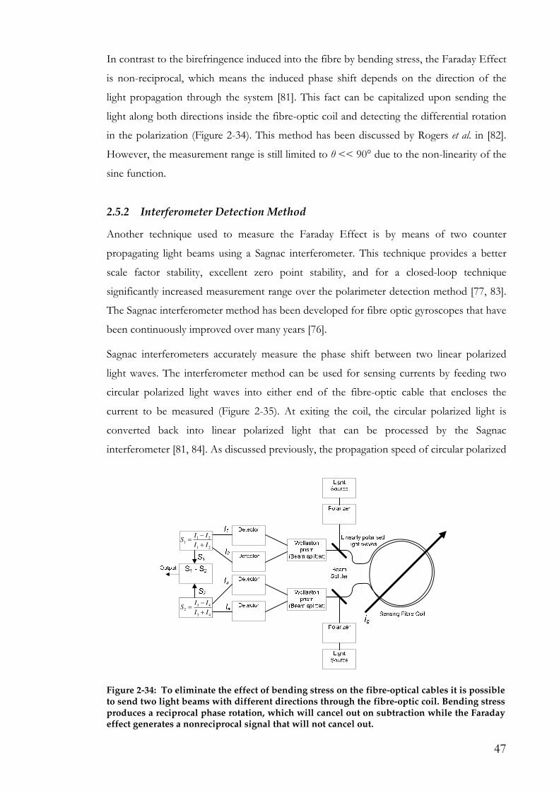
47
In contrast to the birefringence induced into the fibre by bending stress, the Faraday Effect
is non-reciprocal, which means the induced phase shift depends on the direction of the
light propagation through the system [81]. This fact can be capitalized upon sending the
light along both directions inside the fibre-optic coil and detecting the differential rotation
in the polarization (Figure 2-34). This method has been discussed by Rogers et al. in [82].
However, the measurement range is still limited to θ << 90° due to the non-linearity of the
sine function.
2.5.2 Interferometer Detection Method
Another technique used to measure the Faraday Effect is by means of two counter
propagating light beams using a Sagnac interferometer. This technique provides a better
scale factor stability, excellent zero point stability, and for a closed-loop technique
significantly increased measurement range over the polarimeter detection method [77, 83].
The Sagnac interferometer method has been developed for fibre optic gyroscopes that have
been continuously improved over many years [76].
Sagnac interferometers accurately measure the phase shift between two linear polarized
light waves. The interferometer method can be used for sensing currents by feeding two
circular polarized light waves into either end of the fibre-optic cable that encloses the
current to be measured (Figure 2-35). At exiting the coil, the circular polarized light is
converted back into linear polarized light that can be processed by the Sagnac
interferometer [81, 84]. As discussed previously, the propagation speed of circular polarized
21
211
II
IIS
+
−=
43
432
II
IIS
+
−=
Figure 2-34: To eliminate the effect of bending stress on the fibre-optical cables it is possible to send two light beams with different directions through the fibre-optic coil. Bending stress produces a reciprocal phase rotation, which will cancel out on subtraction while the Faraday effect generates a nonreciprocal signal that will not cancel out.

48
light is altered by the Faraday Effect, which means that one light wave travels at increased
speed whereas the other one is slowed down. Therefore a phase shift between the two light
waves results that is a direct measure for the magnitude of the magnetic field or current
respectively.
The Sagnac interferometer linearly polarizes the source light and splits it into two equal
beams, which are converted into circularly polarized beams using quarter wave (λ/4)
retarders. Once the two light beams exit the coil, they are converted back into linear light
waves, which now have a phase difference proportional to the current ic due to the Faraday
Effect. The differential phase shift ∆φs between the returning linear polarized light waves
can be described according to [84]:
∫ =⋅=∆C
cS VNisdHVN .2rr
φ (2-28)
As an example, the Faraday Effect induces a phase difference of 2.65 µrad/A at a
wavelength of 850 nm for fused silica fibre [85]. The open-loop Sagnac interferometer
measures the phase shift ∆φs by bringing the retrieved linear polarized light to interference
(Figure 2-35) [81]. Using this system the detected interfered light beams may cancel each
other at 180° phase shift or lead to a constructive interference at 0°. The detected light
intensity Id resulting from the interference is determined by:
( ),cos12
0sd
II φ∆+= (2-29)
where I0 is the light intensity of the light source [84]. Naturally, this formula is only an
approximation since no losses within the fibres-optic cable and components are
considered. A major problem of this detection method is the very small sensitivity around
∆φs = 0. For this reason a periodic phase modulation is carried out as shown in Figure 2-35
Figure 2-35: Schematic of an open-loop Sagnac interferometer that measures the phase shift between circular polarized light waves, which is proportional to the magnetic field. A phase modulator is required to obtain a linear relation between the phase shift and detection signal.

49
that allows it to generate a linear output from the detected signal by building the ratio of
the first and second harmonic amplitude level [76, 84]. The phase modulator can be
realized by winding fibre around a piezoelectric transducer. However, the measurement is
only linear for ∆φs << 90°.
The closed-loop method pushes the interferometer approach one step further by
compensating the phase shift induced by the Faraday Effect by means of a non-reciprocal
frequency shifter (Figure 2-36). The signal processor implements a control loop that adjusts
the phase shift using the frequency shifter until both light beams are in phase. Accordingly,
the control signal for the frequency shifter, is a direct measure for the phase shift ∆φs, and
is linear over a much larger range than the open-loop principle [76].
Although the method of feeding the light into both ends of the fibre-optic cable enhances
the immunity against bending stress inside the fibre, the discussed detection methods are
still vulnerable against vibrations and thermal drift of the Verdet constant. In addition
acoustic vibrations at the second and third harmonic are widespread in power distribution
systems, and may deteriorate the measurement accuracy of the detection methods [82, 86].
The thermal drift can be compensated by employing a retarder with counteracting
temperature behaviour or by using a dedicated temperature sensor that allows a
compensation within the signal processor [78, 84]. Using these methods, an overall sensing
accuracy of better than 0.1% can be achieved as demonstrated in Figure 2-38.
The vibration problem can be eased by using a so-called reflective or in-line sensor
arrangement as shown in Figure 2-37 [83, 87]. In this configuration RHCP and LHCP light
waves are fed into the fibre coil from the same end of the coil. At the mirror attached to
the other end of the coil, the light beams are reflected and their polarizations states
swapped from RHCP polarized to LHCP and vice versa. Accordingly, the total phase shift
Figure 2-36: In a closed-loop Sagnac interferometer the phase shift induced by the Faraday effect is compensated by means of a frequency shifter, and thus achieves a linear response over a much larger measurement range than polarimeter and open-loop interferometer detection methods.

50
is two times that of the original Sagnac interferometer because the light travels through the
coil two times:
.4 cS VNi=∆φ (2-30)
At the same time the sensitivity of this configuration against vibrations is much reduced
because the differential phase of two orthogonal light waves is around 1000 times less
disturbed than the phase of the two independent light waves of the Sagnac interferometer
(Figure 2-39) [84]. A coupler, delay line and 90° splice is required to convert the orthogonal
linear polarized light waves to two separate linear polarized light waves that can be
processed by the Sagnac interferometer. The phase shift between the linear polarized light
waves can be measured using a standard open-loop or closed-loop Sagnac interferometer
method as discussed previously.
λ\4
Retarder
icSensing Fibre Coil
Orthogonal linear
polarised light waves
Right-hand and left-hand
circular polarised light waves
Mirror
Delay
90° Splice
Sagnac Interferometer
(open-loop / closed-loop)
Output
Linearly polarised
light waves
Coupler
Figure 2-37: Schematic of a reflective interferometer where left- and right-hand circular polarized light waves are feed into the coil at one end and reflected by a mirror at the other end. This technique has vastly improved immunity to vibrations and a doubling of the sensitivity over the original Sagnac method since the light effectively travels two times through the coil.
-20 0 20 40 60 800.992
0.996
1.000
1.004
1.008
Constant current
Sig
na
l (n
orm
aliz
ed)
Coil temperature (°C)
+/-0.1%
Figure 2-38: Temperature dependence of a Sagnac interferometer with temperature compensation, capable of an overall accuracy of better than 0.1% over a wide temperature range [78].

51
2.5.3 Conclusion for Faraday Effect based Current Sensors
In order to avoid stress on the fibre-optic cable, the cable is packaged so as to protect the
cable from any stress due to mounting and transportation of the current sensor. The fibre-
optic current sensor, nevertheless, allows a significant reduction in power consumption and
bulk compared with alternative technologies that are used in power distribution systems
(Figure 2-40). For smaller current magnitudes, other principles are more attractive since
they are less expensive, and the fibre-optic principle would require many turns to provide
satisfactory sensitivity. Moreover, this would involve the use of a special and expensive
fibre optical cable in order to avoid bending stress, which otherwise deteriorates the
performance. Increased sensitivity can also be achieved by using experimentally available
fibre optical cables with higher Verdet constant. However, these experimental cables only
allow a gain in sensitivity of less than ten at the expense of an increased thermal drift. As
pointed out before, fibre-optic current sensors are especially useful in high voltage systems
because of the inherent electrical isolation, and in systems with high electro-magnetic-
inference levels. They are usually employed in power metering, fault detection and electro-
winning applications.
2.6 Discussion
This chapter critically reviewed conventional current sensors. In this section, the usefulness
of these current sensors for sensing currents in power converters is discussed using
performance data found in datasheets of commercially available current sensors. It should
be pointed out that from each technology the most inexpensive sensor, and not the one
with the best performance has been considered for the comparison because of the cost
0 2 4 6 8 10
0
5
10
15
vibration direction :
vibration frequency = 50 Hz
Sagnac sensor
reflective sensor
Eq
uiv
ale
nt
Cu
rren
t (A
rm
s)
Acceleration (g)
Figure 2-39: Current errors generated via vibrations of the coils for Sagnac and reflective interferometers, showing the superior performance of the reflective interferometer over the classical Sagnac interferometer [84].

52
pressure in the power converter market.
TABLE 2-II compares commercially available current sensors with 10 A nominal current
and measurement bandwidth around 100 kHz that may be employed to measure currents
inside a PFC stage or to measure the primary side current of a DC-DC converter. TABLE
2-III compares 200 A current sensors with more than 1 kHz bandwidth that can be used to
detect the output current of a power converter with DC output. For completeness, the
proposed current sensing techniques that are discussed later in this thesis are also included
(shaded columns).
For the shunt resistor the additional effort needed to amplify the signal to a level
compatible for an analogue-to-digital converter has been included in both comparisons.
This explains why a shunt resistor solution for the 10 A current range is more expensive
than expected because the employed amplifier needs to exhibit a large gain-bandwidth
product to achieve at least 100 kHz overall measurement bandwidth. As mentioned before,
the use of a shunt resistor involves a trade-off between amplification cost, power loss and
measurement bandwidth. For instance, it is feasible to increase the shunt resistor resistance
at the cost of more power loss in order to reduce the gain requirement for the amplification
stage. The depicted shunt resistor data is therefore just one example that meets the
Figure 2-40: Commercial available fibre-optic-current-sensors (FOCSs) capable of measuring several hundred kA (photo courtesy ABB, Inc.).

53
specified performance goals, and could be optimised for cost, power loss or bandwidth.
Mentioned many times before, current sensing in power converters is mainly focused on
cost and size to increase power density and lower the system cost. It can be seen in
TABLE 2-II and TABLE 2-III, that open-loop Hall Effect, fluxgate and AMR current
sensors are far too expensive compared with shunt resistors and CT solutions that are
currently employed in power converters. Due to the high cost, closed-loop Hall Effect
sensors are not considered in TABLE 2-II and TABLE 2-III. The listed commercial
fluxgate current sensor is a highly accurate model that demonstrates the capability of the
fluxgate current sense principle. Lower cost models from VAC, Honeywell and LEM are
also available but not listed. The performance and cost of such fluxgate current sensors is
similar to that of closed loop Hall Effect current sensors. Fibre-optic current sensors are
not considered since they are very expensive, and thus not suitable for integration into
power converter.
An alternative are inexpensive magnetic field sensing ICs that allow the measurement of
currents from one ampere up to several hundred amperes. However, it has been shown
that skin effect and parasitic magnetic fields deteriorate the measurement accuracy. In
modern power converters with high package density and several sources of magnetic fields,
it is very difficult to employ this current sensing technique even with shielding. Moreover,
the price comparison in TABLE 2-II and TABLE 2-III reveals that the naked magnetic
field sensing IC without additional shielding is already more expensive than contemporary
shunt resistor based current sensors.
Recently, integrated core-less Hall Effect current sensors entered the market, e.g. the
ACS713 (10 A) and ACS755 (200 A) from Allegro Microsystems that are low priced, small
in size and provide electrical isolation. This type of current sensor usually works after the
open-loop core-less principle and exhibits better magnetic noise immunity than magnetic
field sensing ICs. Moreover, the sensor is calibrated during the production process, and
thus provides good initial measurement accuracy. Unfortunately, the datasheet does not
provide any data about the magnetic noise immunity. For the AMR CDS4150 current
sensor, which also works after the open-loop core-less principle, the datasheet reveals that
the effectiveness of the magnetic shield is limited and the usual background noise in a
power converter may deteriorate the accuracy. Accordingly, it has to be assumed that the
same restriction applies for the ACS713 and ACS755. Another significant shortcoming is
the fact that the whole current has to flow through the sensor housing, and thus generates
conduction power loss. As an example, the internal resistance of the ACS755 current
sensor is 100 µΩ, which results in a conduction power loss of 4 W at 200 A. The AMR

54
current sensor CDS4150 exhibits a conduction resistance for the primary current of 70 µΩ,
resulting in 2.8 W conduction losses. In addition, core-less current sensors with integrated
primary conductor have limited pulse current capability as demonstrated in TABLE 2-II
and TABLE 2-III.
A few more words have to be said about the 200 A shunt resistor based current sensor.
One surprising fact is that the shunt resistor approach is not much more expensive for the
200 A than for the 10 A measurement range. This is due to the fact, that the 200 A sensor
does not require high bandwidth. By sacrificing the bandwidth, which is now determined
by the amplifier and not the shunt resistor’s parasitic inductance, a less expensive amplifier
can be chosen. The shunt resistor itself would allow a bandwidth up to 10 kHz.
In conclusion, the comparison indicates that despite the improvement achieved in current
sensing, the shunt resistor and CT are still presently the only choice in price sensitive
power converter applications. Due to the significant power loss in shunt resistors and the
unfortunate duty cycle limitation and insertion inductance of the CT, current sensors
notably reduce the efficiency of modern power converter.

55
TA
BL
E 2
-II:
CO
MP
AR
ISO
N B
ET
WE
EN
CO
MM
ON
CU
RR
EN
T S
EN
SIN
G S
OL
UT
ION
S A
BL
E T
O M
EA
SU
RE
CU
RR
EN
TS
UP
TO
10
AM
PE
RE
S A
T 1
00K
VO
LU
ME
Sh
unt R
esis
tor
1,14
H
all E
ffec
t Mod
ule
2 (O
pen-
loop
) H
all E
ffec
t IC
3 (C
ore-
less
) H
all E
ffec
t IC
4
(H-f
ield
) G
MR
Eff
ect I
C 5
,14
(H-f
ield
) A
MR
Eff
ect
Mod
ule
6
(C
ore-
less
)
Flu
xgat
e M
odul
e 7
Cur
rent
T
rans
form
er 8
,14
Tra
nsfo
rmer
Bas
ed
DC
Cur
rent
Sen
sor
9,14
Ban
dwid
th (-
3dB
) 10
0 kH
z 50
kH
z 80
kH
z 10
5 kH
z <
1 M
Hz
500
kHz
500
kHz
< 2
0 M
Hz
< 1
MH
z
DC
Cap
able
Y
es
Yes
Y
es
Yes
Y
es
Yes
Y
es
No
Yes
Ove
rall
Acc
urac
y at
T
a = 2
5 °C
<
±1%
10
< ±
1% 12
<
±1.
5%
(Aft
er C
alib
ratio
n)
< ±
1.5%
(Aft
er C
alib
ratio
n)
< ±
4%
(A
fter
cal
ibra
tion)
<
±0.
8%
< ±
0.1%
(Inc
ludi
ng th
erm
al
drif
t)
< ±
0.5%
<
±0.
5%
Tem
p. C
oeff
icie
nt
@ I
nom
15
< ±
100
ppm
/K
< ±
1000
ppm
/K
< ±
180
ppm
/K
< ±
400
ppm
/K
< +
1400
ppm
/K
< ±
190
ppm
/K
N/A
<
±25
ppm
/K
< -
25 p
pm/K
Cos
t [U
SD]
$0.7
0 10
$4
.30
$0.9
6 $1
.50
$4 10
$7
.60
>$1
00
$0.5
0 $0
.50
10
Size
0.
5 cm
3 2.
6 cm
3 0.
1 cm
3 0.
1 cm
3 0.
5 cm
3 2.
7 cm
3 50
0 cm
3 1
cm3
1 cm
3
Isol
ated
N
o Y
es
Yes
Y
es
Yes
Y
es
Yes
Y
es
Yes
Pul
se C
urre
nt
Rat
ing
5x n
omin
al c
urre
nt
for
5 s
3x n
omin
al c
urre
nt 13
5x
nom
inal
cur
rent
fo
r 10
0 m
s N
o el
ectr
ical
co
nnec
tion
No
elec
tric
al
conn
ectio
n 10
x no
min
al
curr
ent f
or
3 m
s N
o el
ectr
ical
co
nnec
tion
No
elec
tric
al
conn
ectio
n N
o el
ectr
ical
co
nnec
tion
Ext
erna
l mag
netic
fi
eld
imm
unity
G
ood
Goo
d F
air
Poo
r P
oor
Fai
r G
ood
Goo
d G
ood
Pow
er L
oss
@ I
nom
0.5
W
0.11
W
0.17
W
0.07
5 W
<
0.1
W
0.41
W
2 W
<
0.3
W
< 0
.4 W
Ope
ratin
g T
empe
ratu
re [°
C]
-40.
.+12
0 -4
0..+
85
-40.
.+85
-4
0..+
125
-50.
.+12
5 -2
5..+
85
-25.
.+70
-4
0..+
125
-40.
.+15
0
Pow
er S
uppl
y 5
V
5 V
5
V
5 V
5
V
5 V
±
15 V
N
/A
12 V
1 5
mΩ
Shu
nt R
esis
tor
WSL
2512
fro
m V
isha
y (L
p <
5 n
H) &
OP
A37
6 (G
BW
: 5.5
MH
z) o
pera
tiona
l am
plif
ier
from
Tex
as I
nstr
umen
ts
2 H
MS
10-P
fro
m L
EM
3
AC
S713
fro
m A
llegr
o 4
FH
S 40
P/S
P60
0 fr
om L
EM
5
AA
004-
02 f
rom
NV
E (
mag
netic
fie
ld s
enso
r). I
ts l
inea
r ra
nge
goes
fro
m 0
.5 m
T t
o 3.
5 m
T,
and
thus
nee
ds a
per
man
ent
mag
netic
fie
ld (
e.g.
mag
net)
to
gene
rate
0.5
mT
off
set.
Mor
eove
r, a
sta
ble
refe
renc
e vo
ltage
is
nece
ssar
y to
ge
nera
te th
e su
pply
vol
tage
. 6
CD
S401
0 fr
om S
ensi
tec
7 C
T-1
0T f
rom
LE
M
8 10
0:1
turn
s ra
tio, 1
3/7.
5/5-
3C11
tor
oid
core
fro
m F
erro
xcub
e.
9 U
sing
50:
50:1
tra
nsfo
rmer
with
270
1A a
lloy
from
Hita
chi m
etal
s.
10 E
stim
ated
11
Cal
ibra
tion
requ
ired
12
Exc
ludi
ng m
agne
tic o
ffse
t (±
1.2%
) aft
er a
n ov
ercu
rren
t inc
iden
t of
3x
nom
inal
cur
rent
13
Onl
y to
avo
id m
agne
tic o
ffse
t. N
o da
mag
e oc
curs
abo
ve th
is v
alue
. 14
Typ
ical
per
form
ance
giv
en th
e lis
ted
cost
for
the
impl
emen
tatio
n 15
Inc
ludi
ng o
ffse
t and
sen
sitiv
ity d
rift

56
2.6.1 Summary
This literature review shows that measuring currents in power converters is a challenging
task. In the past, where power converters have used analogue control, the shunt resistor
was the ideal choice in many applications due to its simplicity and accuracy. At present,
there is no satisfactory replacement available for shunt resistors in digital controlled power
converters. Alternative techniques come at increased size, less performance, and, most
important, higher cost.
However, two promising technologies for low-cost current sensing have been identified:
1. The copper trace current sense approach
The copper trace current sense approach has the same working principle as a shunt resistor
but comes at lower cost and is inherently lossless, which allows the measurement of very
large currents. However, it is not clear if sufficient accuracy can be achieved by means of a
temperature sensor to correct for thermal drift of copper. Also the dynamic performance
of such an arrangement needs to be determined and, if necessary, improved. The copper
trace current sense approach has been investigated in Chapter 3.
2. Current transformer based DC current sensor
Another interesting candidate is the CT technology. While CTs are normally unable to
measure DC current, techniques exist to allow the measurement of DC. One such example
has been presented by Severns at APEC’86 [88]. The advantages of this circuit are low-
cost, galvanic isolation and high accuracy. However, a way has to be found to get around
the inability to measure small currents. A complete theoretical investigation of the working
principle with an extension to measure currents down to zero is presented in Chapter 5.

57
TA
BL
E 2
-III
: C
OM
PA
RIS
ON
BE
TW
EE
N C
OM
MO
N C
UR
RE
NT
SE
NS
ING
SO
LU
TIO
NS
AB
LE
TO
ME
AS
UR
E C
UR
RE
NT
S U
P T
O 2
00 A
MP
ER
E A
T 1
00K
VO
LU
ME
Sh
unt R
esis
tor1
, 14
Hal
l Eff
ect M
odul
e2
(Ope
n-lo
op)
Hal
l Eff
ect I
C3
(Cor
e-le
ss)
Hal
l Eff
ect I
C4
(H-f
ield
) G
MR
Eff
ect I
C5,
14
(H-f
ield
) A
MR
Eff
ect
Mod
ule6
(Cor
e-le
ss)
Tra
nsfo
rmer
Bas
ed
DC
Cur
rent
Se
nsor
7, 1
4
Cop
per
Tra
ce
Pri
ncip
le 1
4 M
odif
ied
Out
put
Indu
ctor
Cur
rent
Se
nsin
g 14
Ban
dwid
th (-
3dB
) 5
kHz
20 k
Hz
35 k
Hz
105
kHz
< 1
MH
z 40
0 kH
z 10
kH
z
5
kHz
5 kH
z
DC
Cap
able
Y
es
Yes
Y
es
Yes
Y
es
Yes
Y
es
Yes
Y
es
Ove
rall
Acc
urac
y at
T
a = 2
5°C
<
±1%
(Aft
er C
alib
ratio
n)
< ±
1% 12
<
±1%
<
±1.
5%
(Aft
er C
alib
ratio
n)
< ±
4%
(A
fter
cal
ibra
tion)
<
0.8
%
< ±
0.5%
<
±1%
(Aft
er C
alib
ratio
n)
< ±
1% 8
(A
fter
Cal
ibra
tion)
Tem
p. C
oeff
icie
nt
@ I
nom
15
< ±
150
ppm
/K
< ±
820
ppm
/K
< ±
610
ppm
/K
< ±
400
ppm
/K
< +
1400
ppm
/K
< ±
190
ppm
/K
< -
5 pp
m/K
<
±15
0 pp
m/K
8 <
±15
0 pp
m/K
8
Cos
t [U
SD]
$1
$7.2
0 8
$1.7
0 $1
.50
$4 8
$15
8 $1
8
$0.8
0 8
$0.5
0 8
Size
1
cm3
27 c
m3
2.3
cm3
0.1
cm3
0.5
cm3
5.3
cm3
3 cm
3 0.
5 cm
3 0.
5 cm
3
Isol
ated
N
o Y
es
Yes
Y
es
Yes
Y
es
Yes
N
o N
o
Pul
se C
urre
nt
Rat
ing
3x n
omin
al c
urre
nt
for
140
ms
9 3x
nom
inal
cur
rent
13
5x n
omin
al c
urre
nt
for
12 m
s 8
No
elec
tric
al
conn
ectio
n N
o el
ectr
ical
co
nnec
tion
10x
nom
inal
cu
rren
t for
3 m
s N
o el
ectr
ical
co
nnec
tion
Giv
en b
y co
pper
tr
ace
Giv
en b
y in
duct
or
Ext
erna
l mag
netic
fi
eld
imm
unity
G
ood
Goo
d F
air
Poo
r P
oor
Fai
r G
ood
Goo
d G
ood
Pow
er L
oss
@ I
nom
4 W
0.
11 W
4
W
0.07
5 W
<
0.1
W
3 W
<
1 W
<
0.1
W
< 0
.1 W
Ope
ratin
g T
empe
ratu
re [°
C]
-40.
.+12
5 -4
0..+
105
-20.
.+85
-4
0..+
125
-50.
.+12
5 -5
0..+
85
-40.
.+15
0 -4
0..+
125
-40.
.+12
5
Pow
er S
uppl
y 5
V
5 V
5
V
5 V
5
V
5 V
12
V
5 V
5
V
1 2x
0.2
mΩ
Shu
nt R
esis
tor
BV
S251
2 fr
om I
sabe
llenh
uett
e (L
p <
3 n
H)
& L
MC
6482
ope
ratio
nal a
mpl
ifie
r fr
om N
atio
nal S
emic
ondu
ctor
s 2
HT
FS
200-
P f
rom
LE
M
3 A
CS7
55SC
B-2
00-P
SF f
rom
Alle
gro
Mic
rosy
stem
s 4
FH
S 40
P/S
P60
0 fr
om L
EM
5
AA
004-
02 f
rom
NV
E (
mag
netic
fie
ld s
enso
r). I
ts l
inea
r ra
nge
goes
fro
m 0
.5 m
T t
o 3.
5 m
T,
and
thus
nee
ds a
per
man
ent
mag
netic
fie
ld (
e.g.
mag
net)
to
gene
rate
0.5
mT
off
set.
Mor
eove
r, a
sta
ble
refe
renc
e vo
ltage
is
nece
ssar
y to
ge
nera
te th
e su
pply
vol
tage
. 6
CD
S415
0AC
A-I
A f
rom
Sen
site
c (m
ax. 1
50 A
but
sca
led
for
200
A)
7 U
sing
200
:50:
1 tr
ansf
orm
er w
ith 2
701A
allo
y fr
om H
itach
i met
als.
8
Est
imat
ed
9 M
axim
um 5
joul
e pu
lse
ener
gy
12 E
xclu
ding
mag
netic
off
set (
±0.
5%) a
fter
an
over
curr
ent i
ncid
ent
of 3
x no
min
al c
urre
nt
13 O
nly
to a
void
mag
netic
off
set.
No
dam
age
occu
rs a
bove
this
val
ue.
14 T
ypic
al p
erfo
rman
ce g
iven
the
liste
d co
st f
or th
e im
plem
enta
tion
15 I
nclu
ding
off
set a
nd s
ensi
tivity
dri
ft

58
Chapter 3
Current Sensing Using the Copper Trace Resistance
3.1 Introduction
Despite the ongoing search for new current sensing techniques, surface-mounted shunt
resistors are still the most popular approach in many applications due to their low cost, low
size and high reliability [21]. At high currents only a very small voltage drop is allowed
across the shunt in order to keep the power losses to an acceptable level. Accordingly,
these resistors have values below 1 mΩ. For example, two paralleled surface-mounted 200
µΩ shunt resistors dissipate 5.8 W at 240 A. The manufacturers of these resistors have to
keep the temperature coefficient low to avoid temperature drift due to self-heating or
ambient temperature changes. In addition, the parasitic inductance and skin effect have to
be small, otherwise the bandwidth of the current sensing will be limited. Hence, precise
shunt resistors are sophisticated components, and their cost is significant in low-cost
applications.
A copper trace, on the other hand, is free, neither generates additional power losses nor
needs extra space on the printed-circuit-board (PCB). The challenge in using the copper
trace as an alternative to a dedicated shunt resistor is the very small magnitude of the
voltage drop across the trace, and other undesirable physical effects that need to be
addressed within the measurement technique [89]. The following effects may deteriorate
the AC and DC performance of the current measurement:
• Temperature drift of copper (DC), which is the most obvious problem due to the
high temperature coefficient of resistance for copper (3930 ppm/K [90]).
• Initial tolerance of the resistance value (DC) is an unknown due to variations in
cross-sectional area and length generated by large production tolerances.

59
• Induced currents into the sense circuit caused by varying localized magnetic fields
(AC).
• Skin effect (AC), which alters the transient performance of this sense method since
it changes the apparent resistance as a function of frequency.
• Seebeck effect (DC), which may introduce a temperature dependent offset into the
sense voltage, if there is a temperature difference between the two connection
points of the sense wire.
These obstacles may be the reason why there are only a limited number of publications on
this technique available. Spaziani [23] provided design equations and recommendations for
a PCB copper shunt resistor, while not considering the transient performance. He
concluded that this approach is not suitable for accurate applications due to the high
temperature drift of the copper resistance. Eirea [24] tried to overcome the temperature
drift problem by using the input current of the power converter to calibrate the resistance
of the copper trace. However, the proposed estimation loop has to be disabled at small
currents, since the estimation loop starts to drift because of the offset voltage of the
employed amplifier. In this condition, the temperature coefficient of the copper resistance
will alter the measurement accuracy. This principle is not well suited for isolated power
converter topologies, since it would entail an isolated measurement technique for the input
current. DC current sensors providing isolation are notably more expensive than a simple
shunt resistor.
The aim of this chapter is to provide a thorough theoretical and experimental investigation
of the use of a copper trace for current sensing and how it may be implemented.
3.2 Proposed Method
To overcome the above-mentioned obstacles, the use of a temperature sensor to
compensate for the thermal drift of the copper resistance is proposed, and a compensation
network that rectifies distortions introduced by the skin effect and voltage induced into the
sense wire. Temperature compensation has been successfully used for high precision shunt
resistors, where it reduced the measurement uncertainty by a factor of five [91]. Moreover,
it is shown that the distance d between the forward and return current path has significant
influence on the voltage induced into the sense wires.

60
Sensing the temperature of a copper trace embedded into a PCB is certainly a difficult task
to accomplish. However, at current levels beyond 100 A, it is inefficient to distribute this
current with copper traces, and massive busbars of copper are used. Such busbars have the
desirable property of a very high thermal conductivity and heat capacity, which ensures that
the temperature along the busbar is almost constant. This effectively reduces problems
with the Seebeck effect, and means that the system is relatively insensitive to the position
of the temperature sensor. A block diagram of the proposed method is shown in Figure 3-1
which includes a compensation network, an amplifier and a microcontroller (µC) with
integrated analogue-to-digital converter (ADC).
The performance of the proposed techniques is investigated within the next three sections.
In Section 3.3 it is demonstrated how the temperature drift of copper can be compensated,
and what other physical effects need to be considered. Section 3.4 describes how the
parameters of the proposed temperature correction function can be evaluated during the
production process. The dynamic behaviour is investigated within Section 3.5. The
bandwidth of the proposed current sense method has been measured and simulated and it
has been proved that a compensation network similar to the lossless inductor current
sensing technique [13] can drastically improve the dynamic behaviour.
3.3 Static Performance
The first and most obvious problem is that the static accuracy is influenced by the thermal
drift and initial tolerance of the busbar resistance. During production process, the initial
resistance of the busbar cannot be sustained with sufficient accuracy. Accordingly, a
calibration has to be undertaken that identifies the DC resistance. Experimental
measurements have further shown that the thermal resistance between the temperature
Figure 3-1: Proposed busbar current sense method that includes a temperature sensor to eliminate the temperature drift of the copper resistance. The compensation network rectifies distortions introduced by the skin effect, proximity effect and voltage induced into the sense wires.

61
sensor and the busbar needs to be considered for highest precision.
3.3.1 Temperature Sensing Requirements
A straightforward solution to compensate the temperature drift of the busbar is to sense its
temperature Tb and combine this measurement with the known temperature coefficient of
resistance for copper. The resistance of the busbar is given by:
( ).125 TRRT ∆+= α (3-1)
RT is the apparent resistance of the busbar, R25 the resistance of the busbar at 25°C copper
temperature, α the temperature coefficient of resistance of copper (3930 ppm/K) and ∆T
the difference between the actual copper temperature Tb and 25°C. If ∆T can be measured
with sufficient precision, the deviation of the busbar resistance can be calculated, and the
apparent resistance predicted with high accuracy. Precise temperature sensing can become
very expensive and complicated. Fortunately, the tolerance of the temperature sensing and
the temperature coefficient of copper are multiplied. The apparent busbar resistance RT
considering the temperature measurement error εT is:
( )( ).1125 TT TRR εα +∆+= (3-2)
This yields an error εR in the calculated apparent busbar resistance of:
.1
25
T
T
R
TR T
T
TR
∆+
∆=
∆=
α
εαεαε (3-3)
Thus, in order to attain a certain current measurement accuracy, the maximum error εT of
the temperature sensor is given by:
( ).
1
T
T RT
∆
∆+=
α
εαε (3-4)
For a temperature deviation ∆T of ±75 K and a maximum allowed resistance error εR of
±1%, the temperature error εT has to be lower than ±4.4% or ±3.3 K. This level of
accuracy is easily obtainable using low cost temperature sensors. It is important to
understand, that the offset error of the temperature sensor has no influence on the
measurement accuracy since a relative temperature ∆T, referring to the calibrated value Tr,
is measured. Therefore, the linearity and gain error of the temperature sensor determines
the accuracy of the current measurement. By pushing this approach one-step further, one
can say that the temperature sensor does not even need to be linear and can be
approximated with a polynomial, as long as the measurement characteristic is reproducible
and is not subject to device-to-device variations.

62
3.3.2 Temperature Isolation of the Sensor
Initally it has been thought that the static accuracy is solely given by the above-mentioned
theory. Figure 3-2 shows the measurement results of a hardware experiment that was
carried out at a constant ambient temperature of 25°C. The reference current was
calibrated using a shunt resistor with 1 % initial tolerance and 20 ppm/K thermal drift. In
order to minimise any thermal drift of the measurement equipment, an external fan was
employed to improve thermal transfer to the environment and minimise self-heating
effects, so that the thermal drift of the shunt resistor could be neglected compared with the
thermal drift of the copper busbar. A thermocouple was used to measure the busbar
temperature. The busbar was heated using high currents, followed by a short interruption
wherein the desired current was set and the readings taken. The heat capacitance of the
busbar held its temperature constant during this short period. Aside from the noise due to
random errors in the measurement method, a steadily increasing systematic error can be
observed within Figure 3-2. The same measurement was repeated later, using a low-cost
LM335 temperature sensor that comes within a TO-92 package in Figure 3-3. This sensor
was attached to the busbar using thermal paste to lower the thermal resistance. Again a
systematic error is observed that increases linearly with the busbar temperature, but this
time the slope of the error was larger. This phenomenon can be explained in terms of the
thermal isolation between the temperature sensor and the busbar, which leads to a
temperature drop between the busbar and the temperature sensor. Due to the
configuration and operation of the temperature sensor this temperature drop is almost
always observed as an underestimation of the busbar temperature. This is also the reason
for the difference of the error slope between Figure 3-2 and Figure 3-3, since the
Ta = 25°C
-2.0
-1.0
0.0
1.0
2.0
3.0
4.0
25 30 35 40 45 50 55 60
Busbar Temperature T sensed by a Thermocouple [°C]
Me
asu
rem
en
t E
rro
r [A
]
80A 160A 240A
Figure 3-2: Error in the measured current as a function of the busbar temperature sensed using a thermocouple. The measured current is determined using the temperature to correct for the resistance drift of copper.

63
thermocouple has a lower thermal isolation from the busbar compared with the LM335
sensor.
The temperature sensor is supposed to measures the difference between the actual busbar
temperature Tb and the calibrated reference temperature Tr:
.rb TTT −=∆ (3-5)
In reality, however, the sensed temperature difference ∆Ts underestimates the real
temperature difference ∆T due to the thermal resistance Rth-s between the busbar and the
temperature sensor:
.sthhs RPTT −−∆=∆ (3-6)
Ph is the heat flow through the busbar surface covered by the temperature sensor package.
Ph is proportional to the total power dissipation Pv inside the busbar, with n as the
proportional constant:
.vh nPP = (3-7)
In order to calculate the temperature drop between the busbar and temperature sensor, the
heat power flow Ph has to be known. There are two methods to determine this value:
• Calculating Ph based on the difference between ambient and busbar temperature.
• Calculating the power dissipation using the busbar current and voltage.
Measuring the Ambient Temperature
If the ambient temperature Ta is known, it is feasible to calculate the value of Pv using the
Ta = 25°C
-2.0
-1.0
0.0
1.0
2.0
3.0
4.0
25 30 35 40 45 50 55 60
Busbar Temperature T sensed with an LM335 [°C]
Measu
rem
en
t E
rro
r [A
]
80A 160A 240A
Figure 3-3: Error in the measured current as a function of the busbar temperature sensed using a LM335 temperature sensor. Due to the thermal isolation between busbar and sensor, a larger linear deviation of the measurement error with temperature is observed.

64
thermal resistance Rth-b between the busbar and free air:
.bthvar RPTTT −+=+∆ (3-8)
Solving for the total heat flow Pv yields:
.bth
arv
R
TT∆TP
−
−+= (3-9)
By combining (3-6), (3-7) and (3-9):
.bth
arsths
R
TT∆TnR∆T∆T
−
−
−+−= (3-10)
This equation needs to be solved for the apparent busbar temperature Tb-a using ∆Ts = Tb-a
– Tr:
.r
sthbth
stha
sthbth
bthab T
nRR
nRT
nRR
RT∆T −
−−
−=
−−
−
−−
−−
(3-11)
As expected, this equation yields ∆T = Tb-a – Tr for Rth-s = 0, and thus Tb = Tb-a. One can
introduce the following substitution to simplify (3-11):
.sthbth
bth
nRR
Rk
−−
−
−= (3-12)
Accordingly:
( ) ( ).raaab TTTTk∆T −+−= − (3-13)
This formula is simple to implement into a microcontroller. The value of k can be
identified using a hardware experiment, preferably when Ta = Tr.
Calculating the Total Power Loss
The above-mentioned technique requires the knowledge of the ambient temperature Ta. If
this temperature is not available, it is possible to calculate the temperature underestimation
based on the measured power dissipation inside the busbar. During thermal steady state,
the busbar power loss is equal to the total heat flow Pv, and can be described by the
following formula:
( )TR
V
R
VP s
T
sv
∆+==
α125
22
(3-14)

65
The variable Vs has been chosen intentionally instead of vs, since this formula is only valid
within thermal steady state. If (3-14) is merged with (3-6) and (3-7), a formula is obtained
that does not rely on the ambient temperature at all:
( ).
125
2
TR
VRnTT ssth
s∆+
−∆=∆ −
α (3-15)
This equation can now be computed for ∆T:
( ) .∆TR
VRnα∆T∆Tα∆T s
ssths 01
25
2
2 =
+−−+ − (3-16)
Naturally, this quadratic equation yields two results:
( )
( )
.α
∆TR
VRnαα∆T
α
α∆T∆T
sssth
s
s
2
41
2
1
25
22
++−
±
−=
−
(3-17)
By setting Rth-s = 0, which is the case when the temperature sensor measures the true busbar
temperature Tb, the result has to be ∆T = ∆Ts. One finds that only the solution using
positive sign gives the correct result. Obviously, (3-17) is unduly more complicated to
compute than (3-11) but comes with the advantage that no ambient temperature sensing is
required.
3.3.3 Measurement Results
Using a temperature cabinet and a constant current of 160 A and 200 A respectively, the
applicability of the proposed correction formulas for the thermal steady state has been
verified. It is important to note that the measurement of the reference current was via a
shunt resistor, as stated previously, and this was kept outside the temperature cabinet at a
constant ambient temperature, which means that the measured reference current was not
subject to significant thermal offset. After determining k and Rth-s the results depicted in
Figure 3-4 have been obtained. How k and Rth-s can be determined is explained in the next
section. The two correction functions yield similar results. If no correction formula is
employed, an offset is present that leads to a notable error at 200 A current. At 160 A, the
offset is smaller, since the temperature drop between the temperature sensor and busbar is
proportional to the power loss within the busbar (refer to (3-6)). For this reason the error is
proportional to the square of the current. It can also be observed that the measurement
error decreases at higher temperatures. This can be explained with the precision of the

66
temperature sensor itself. Without optional gain calibration, the employed LM335
temperature sensor has a typical combined gain and non-linearity error of ±2 K between
25 and 125°. Using (3-3), one obtains a theoretical measurement uncertainty of ±1.46 A.
For 240 A maximum current, this is equal to an absolute error of ±0.61%. The reason why
125°C was used as the upper temperature limit is because at 105°C ambient temperature
and 200 A current the busbar temperature was 125°C. Overall, the theory is in good
agreement with the results shown in Figure 3-4.
The accuracy of the busbar current measurement method has been further investigated
during fast temperature changes. The same measurement method as used for Figure 3-3,
which unavoidably exhibits fast changes of the busbar temperature, has been applied at
different ambient temperatures. To account for the thermal isolation of the temperature
sensor, the correction function using the ambient temperature has been implemented
because this method is also valid outside thermal steady state. The results in Figure 3-5
confirm a good accuracy even during fast temperature changes. If these results are
compared with Figure 3-3, it is obvious that the proposed compensation technique leads to
a significantly improved accuracy over the whole temperature range. The results also show
that the measurement error drifts toward negative values at higher ambient temperatures
due to the inherent inaccuracy of the temperature sensor.
3.3.4 Comparison of the Two Correction Techniques
Both correction techniques achieve good static performance. In addition, the technique
using the ambient temperature is also able to track the apparent copper resistant during fast
I = 160 A
-3.0
-2.0
-1.0
0.0
1.0
2.0
3.0
4.0
5.0
6.0
30 40 50 60 70 80 90 100
Ambient Temperature T a [°C]
Measu
rem
en
t E
rro
r [
A]
No Correction
Ambient Temp. Sensing
Steady State Formula
I = 200 A
-3.0
-2.0
-1.0
0.0
1.0
2.0
3.0
4.0
5.0
6.0
30 40 50 60 70 80 90 100
Ambient Temperature T a [°C]
Measu
rem
en
t E
rro
r [
A]
No Correction
Ambient Temp. Sensing
Steady State Formula
Figure 3-4: This measurement shows the measurement error during thermal steady state. The two proposed correction techniques that account for the thermal isolation between the busbar and sensor clearly improve the accuracy especially at high current respective power loss.

67
temperature changes. Whether the additional cost of a second temperature sensor is
justified will depend on the application. The computational cost of either technique is
insignificant given the computational power available in most devices.
3.4 Calibration Procedure
A calibration procedure is necessary to determine the unknown parameters required for the
correction functions introduced in the previous section. Unknown parameters are busbar
resistance R25, amplifier offset voltage Vo and amplifier gain Ag. The amplified voltage drop
va of the busbar is given according to:
( ) oga VTiRAv +∆+= α125 (3-18)
It is not necessary to measure the busbar resistance at 25°C, since the reference
Ta = 30°C
-2.0
-1.0
0.0
1.0
2.0
3.0
4.0
25 30 35 40 45 50 55
Busbar Temperature T sensed with an LM335 [°C]
Measu
rem
en
t E
rro
r [A
]
80A 160A 240A
Ta = 50°C
-2.0
-1.0
0.0
1.0
2.0
3.0
4.0
50 55 60 65 70 75 80
Busbar Temperature T sensed with an LM335 [°C]
Measu
rem
en
t E
rro
r [A
]
80A 160A 240A
Ta = 80°C
-2.0
-1.0
0.0
1.0
2.0
3.0
4.0
75 80 85 90 95 100 105 110
Busbar Temperature T sensed with an LM335 [°C]
Measu
rem
en
t E
rro
r [A
]
80A 160A 240A
Figure 3-5: These measurements show the measurement uncertainty during fast temperature changes at different ambient temperature. The proposed correction technique requiring the knowledge of the ambient temperature has been employed. These measurements confirm that even under dynamic temperature changes the measurement error is small.

68
temperature Tr can be initialized with the actual room temperature during the calibration
process. The temperature difference ∆T is therefore zero at the calibrated busbar
temperature Tr. However, it makes sense to ensure that the ambient temperature is close to
the centre of the specified temperature range of the power converter in order to optimize
the measurement accuracy over the whole temperature range.
The transfer function between i and va is a linear function, consisting of an unknown offset
and gain. The amplifier offset Vo can easily be derived by measuring va at zero current i,
while the term AgR25 can be determined with a second measurement at nonzero output
current i. Even if this current sensing method is inherently able to measure currents down
to zero, the required amplification will be tricky in practise since the output offset voltage
Vo of common operational amplifiers can be negative and subject to additional thermal
drift. Nevertheless, there are operational amplifiers with extremely low thermal drift of the
output voltage available, and electrical circuits that compensate for the negative output
offset by means of adding additional positive offset are known. However, the details of the
amplification are not part of this investigation. More detailed information can be found in
[92]. To achieve best accuracy, the output current during the second measurement is ideally
at around two-third of the maximum specified value. A fast temperature change during the
calibration process is undesirable, which is why it is not a good idea to calibrate at the
maximum output current, as this would cause the busbar temperature to rise quickly.
Additionally, a short current pulse should be used during the second calibration
measurement, just sufficient to let the voltage va reach a steady state, while avoiding any
considerable changes in the busbar temperature.
Also unknown parameters are the temperature correction constants k and nRth-s, which can
be determined during the development process, since these values are reasonably constant
during mass production. Equation (3-13) suggests measuring the value of k when the
ambient temperature is equal to the reference temperature. A measurement that yields a
curve as illustrated in Figure 3-3 can be used to adjust k, so that the smallest measurement
error is achieved. For the correction function solely based on the busbar temperature
measurement, the knowledge of nRth-s is required. Using (3-12) one finds:
( ).
1
k
kRnR bth
sth
−= −
− (3-19)
Rth-b is further given by:
.v
abbth
P
TTR
−=− (3-20)

69
Hence, nRth-s can be evaluated based on simple measurements. The determined calibration
constants are then loaded into the non-volatile memory of the microcontroller.
The calibration procedure has been carried out using three different busbars setups, each of
them employing a different LM335 temperature sensor and different busbar. The obtained
results for the busbar resistance R25 and the correction factor k are depicted in TABLE 3-I.
To verify the suitability of the proposed current measurement technique for mass
production, the average of k has been taken, which was 1.23, to repeat the measurement
that has been carried out in Figure 3-3. This time, however, the ambient temperature
sensing correction technique has been employed. The results for each busbar setup are
shown in Figure 3-6.
The peak absolute measurement error is also depicted in TABLE I. According to these
results, it appears that it is reasonable to use an average value for k during mass production,
determined from a small number of measurements taken throughout the design stage.
3.5 Dynamic Performance
Another important characteristic of any current sensor is its measurement bandwidth.
Physical effects that may limit the bandwidth of the busbar current sense method are skin
effect, proximity effect and the voltage that is induced into the sense wires. The voltage
induced into the sense wires can be quantified using the mutual inductance theory. The
self-inductance of the busbar is meaningless in this application, and thus only the mutual
inductance needs to be considered. The skin effect increases the apparent resistance of the
busbar and thus causes a voltage overshoot. If forward and return currents are located
nearby, the proximity effect takes place, which further increases the apparent resistance.
3.5.1 Mutual Inductance Theory
A source of some confusion is the self-inductance of the busbar. Initially it has been
thought that the self-inductance of the busbar would cause a voltage overshoot to be
detected by the sense wires. Accordingly, by determining the self-inductance of the busbar
using simulation or approximate formulas one should be able to calculate the bandwidth of
TABLE 3-I: MEASURED BUSBAR PARAMETERS
Specimen R25 [µΩ]
Ideal Correction
Factor k
Measurement Uncertainty
at k = 1.23 [A]
Nr 1. 21.9 1.23 ± 0.75
Nr 2. 21.5 1.26 ± 1.49
Nr 3. 21.9 1.20 ± 1.23

70
the proposed current sense method. By doing so, one violates a very basic principle of
electromagnetic theory that has been stated by E. Weber in [93]: “It is important to observe
that inductance of a piece of wire not forming a closed loop has no meaning.” This error
was revealed later during hardware experiments, where there was a consistent disagreement
between the results and the calculated self-inductance. The calculation of the self-
inductance yielded a value of around 30 nH whereas the measurements indicated an
inductance that was ten times smaller.
One has to be aware that the busbar self-inductance is a measure of the flux that couples
into the loop formed by the main current. The enclosed area of this loop is marked as Am
in Figure 3-7. This flux, obviously, is not the same flux that couples into the area As
enclosed by the sense wires, which is also illustrated in Figure 3-7. In conclusion, the
voltage that is induced into the sense wires cannot be calculated using the self-inductance
of the busbar. Ironically, researchers came to that conclusion almost hundred years ago
Specimen Nr. 1
-2.0
-1.0
0.0
1.0
2.0
3.0
4.0
25 30 35 40 45 50
Busbar Temperature T sensed with an LM335 [°C]
Measu
rem
en
t E
rro
r [A
]
80A 160A 240A
Specimen Nr. 2
-2.0
-1.0
0.0
1.0
2.0
3.0
4.0
25 30 35 40 45 50
Busbar Temperature T sensed with an LM335 [°C]
Measu
rem
en
t E
rro
r [A
]
80A 160A 240A
Specimen Nr. 3
-2.0
-1.0
0.0
1.0
2.0
3.0
4.0
25 30 35 40 45 50
Busbar Temperature T sensed with an LM335 [°C]
Measu
rem
en
t E
rro
r [A
]
80A 160A 240A
Figure 3-6: The usefulness of the proposed current sense method for mass production has been verified. Three busbar setups using different LM335 sensor and busbar but the same calibration constant k at 25°C ambient temperature have been tested. Obviously, the variability of the component parameters does not notably degrade the performance.
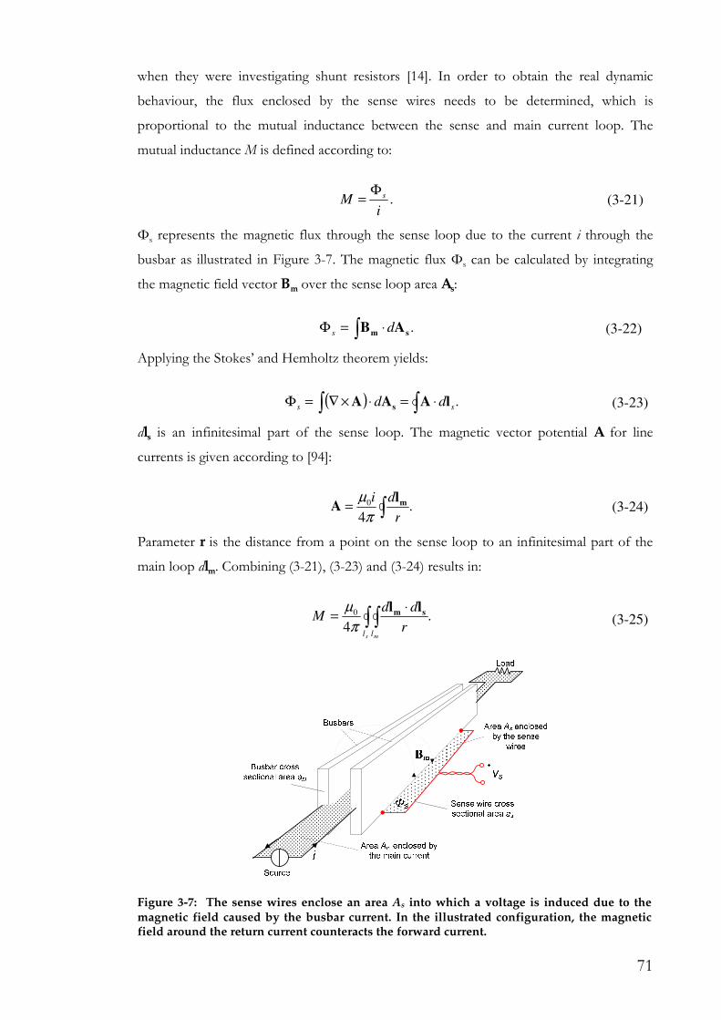
71
when they were investigating shunt resistors [14]. In order to obtain the real dynamic
behaviour, the flux enclosed by the sense wires needs to be determined, which is
proportional to the mutual inductance between the sense and main current loop. The
mutual inductance M is defined according to:
.i
M sΦ= (3-21)
Φs represents the magnetic flux through the sense loop due to the current i through the
busbar as illustrated in Figure 3-7. The magnetic flux Φs can be calculated by integrating
the magnetic field vector Bm over the sense loop area As:
.∫ ⋅=Φ sm AB ds (3-22)
Applying the Stokes’ and Hemholtz theorem yields:
( ) .∫ ∫ ⋅=⋅×∇=Φ ss dd lAAA s (3-23)
dls is an infinitesimal part of the sense loop. The magnetic vector potential A for line
currents is given according to [94]:
.4
0 ∫=r
di mlAπ
µ (3-24)
Parameter r is the distance from a point on the sense loop to an infinitesimal part of the
main loop dlm. Combining (3-21), (3-23) and (3-24) results in:
.4
0 ∫ ∫⋅
=
s ml lr
ddM sm ll
π
µ (3-25)
Figure 3-7: The sense wires enclose an area As into which a voltage is induced due to the magnetic field caused by the busbar current. In the illustrated configuration, the magnetic field around the return current counteracts the forward current.

72
Equation (3-25) is valid for a conductor with an infinitely small diameter. For the employed
busbar, this assumption certainly does not hold. To fix this problem, one can split the
busbar cross sectional area am and sense wire cross sectional area as into infinite small areas
perpendicular to the current flow direction, and integrate over the whole cross section.
Hence, the magnetic vector potential changes to:
,4
0 ∫ ∫=
m ml a
m
m r
dad
a
i mlAπ
µ (3-26)
leading to an average flux of:
.1∫ ∫ ⋅=Φ
s sl a
s
s
s dada
slA (3-27)
Based on that equation, the total mutual inductance becomes:
.4
0 ∫ ∫ ∫ ∫⋅
=
s s m ml a l a
ms
ms
dadar
dd
aaM ms ll
π
µ (3-28)
Unfortunately, this equation is terribly complicated to calculate since no closed form
solution exists usually. Moreover, skin and proximity effects lead to a non-constant current
density inside the conductor, and would require taking into account the frequency
dependent current density. For this reason, it is practical to use a magnetic field simulation
program that discretises dam and das into filaments with finite size. Using a reasonable
number of filaments allows a good representation of the real world behaviour.
In conclusion, the voltage vs measured with the sense wires is the superposition of the
induced voltage due to the mutual inductance, and the resistive voltage drop across the
apparent busbar resistance Ra. In the s-domain, the Laplace transformed sense voltage Vs(s)
is given by:
( ) ( )( ).)()( fsMfRsIsV as += (3-29)
Both, the busbar resistance and the mutual inductance are frequency dependent due to the
skin and proximity effects. The mutual inductance further depends on the actual geometry
of main and sense loops.
3.5.2 Simulation Results
To calculate the mutual inductance M between the sense wire and main current loop the
inductance analysis programs FastHenry [95] has been employed, using the busbar
parameters depicted in Figure 3-1. The self-inductance of the sense loop can be neglected

73
because the sense current is very small, and thus the induced voltage due to that current
irrelevant. Figure 3-8 shows the simulation results for the apparent busbar resistance and
the mutual inductance as a function of frequency. In a first simulation it was assumed that
the busbar conducting the return current is far away, so that only the magnetic field from
the forward current couples into the sense loop. Experimental results showed that this was
the case when the distance between the forward and return paths exceeded 55 mm, and
thus may effectively occur in practice. For the second simulation, also shown in Figure 3-8,
the busbars have been located parallel to each other with a small separation distance d of 2
mm. The simulation confirms that moving forward and return conductor closer together
significantly reduces the mutual inductance since the magnetic fields cancel each other. The
Disadvantage is the fact that at a small separation distance (d = 2 mm) the apparent busbar
resistance is slightly increased at high frequencies due to the proximity effect. It is
interesting to note that the mutual inductance M increases at higher frequencies due to skin
and proximity effect.
Based on the simulation results illustrated in Figure 3-8, the frequency response of the
busbar current sense method has been calculated. Figure 3-9 and Figure 3-10 show the
bode plots for a distance d between the busbars of >55mm (effectively equivalent to
infinite separation) and 2 mm respectively. The gain G of the busbar has been calculated
using the following formula:
( ) ( )( )
.0
log20=
+=
fR
fsMfRG
a
a (3-30)
On the other hand, the phase angle φ is given by:
0.0
0.5
1.0
1.5
2.0
2.5
1 10 100 1000 10000 100000 1000000
Frequency [Hz]
Mu
tua
l In
du
cta
nc
e M
[n
H]
0
100
200
300
400
500
600
700
Ap
pa
ren
t B
us
ba
r R
es
ista
nc
e R
a [
uΩΩ ΩΩ
]
d > 55 mm
(dotted lines)
d = 2 mm
Figure 3-8: The mutual inductance of the sense loop, and the busbar resistance as a function of frequency have been simulated with FastHenry. The results show that by locating the return and forward current path parallel to each other with a separation distance of 2 mm the mutual inductance can be significantly reduced.

74
( )( )
.atan
=
fR
fM
a
ωϕ (3-31)
Naturally, the bandwidth of the configuration having the two busbars located 2 mm apart
is higher due to the lower mutual inductance. The bandwidth is defined at the corner
frequency, which is given where the gain G has increased by 3 dB. That is the case around
1 kHz for d > 55m. and 2 kHz for d = 2 mm.
3.5.3 Compensation Network
Looking at the simulated transfer functions of Figure 3-9 and Figure 3-10 it becomes
apparent that the mutual inductance dominates the frequency response. Hence, the gain
and phase can be corrected employing a compensation network that consists of a first
order low-pass filter. Such a low-pass filter can be built with a simple RC-network. The
values of this low-pass filter have been derived using a least-mean-square curve fitting
function. The resulting simulated frequency response using these values is shown in Figure
3-9 and Figure 3-10. In practice, however, it is more convenient to use an approximate
formula to calculate the values of the low-pass filter, and optimize them using a hardware
experiment. Since the geometries of the busbar and sense loop are fairly constant during
the production process, these values need to be evaluated only once during the
100
101
102
103
104
105
106
-10
0
10
20
30
40
50
60
Gain
[dB
]
d > 55 mm
Simulated
Simulated 1st Order Comp. NW
Measured
100
101
102
103
104
105
106
-50
0
50
100
Phase S
hift
[°]
Frequency [Hz]
Figure 3-9: Bode plot of the measurement bandwidth with and without compensation network at distance of >55 mm between forward and return current.

75
development stage. A starting point for the values of the RC-circuit can be found using:
.max
25
max11
l
Ma
R
MCR m
ρ== (3-32)
R1 and C1 are the values of the RC compensation network, Mmax the maximum mutual
inductance derived from the simulation, l the distance between the two sense connections
(Figure 3-1) and ρ the resistivity of copper. However, this formula assumes that the skin
effect is negligible compared with the mutual inductance, which means that for small
distances between forward and return conductor, where the mutual inductance is small, the
result deviates significantly from the optimised value since this assumption is no longer
valid
3.5.4 Frequency Response Verification
Using a hardware experiment the frequency response of the sense voltage vs has been
measured and compared with the simulation results within Figure 3-9 and Figure 3-10. The
measurement is in good agreement with the simulation, though the accuracy of the phase
measurement was moderate due to the small voltage drop across the busbar. Moreover, it
was not possible to verify the frequency response above 20 kHz due to the difficulty of
producing such a fast changing current at such a large amplitude. The frequency response
using the proposed compensation method could not be measured at all since it was not
100
101
102
103
104
105
106
-10
0
10
20
30
40
50
60
Gain
[dB
]
d = 2 mm
Simulated
Simulated 1st Order Comp. NW
Measured
100
101
102
103
104
105
106
-50
0
50
100
Phase S
hift
[°]
Frequency [Hz]
Figure 3-10: Bode plot of the measurement bandwidth with and without compensation network at a distance of 2 mm between forward and return current.

76
possible to detect the very small resulting voltages with sufficient accuracy. For this reason
the working principle of the compensation network has been verified in the time domain as
shown below.
The frequency response demonstrates that the mutual inductance M dominates the
behaviour even though the busbar resistance increases significantly due to skin effect. This
is because the skin effect is proportional to the square root of the frequency whilst the
reactance due to the mutual inductance increases linearly.
3.5.5 Time-Domain Measurements
By applying a current step, one can assess the transient performance of the proposed
current sense method. In Figure 3-11, the results for a distance d between the busbars of
>55mm are shown. Without a compensation network, a significant overshoot occurs that
may accidentally trigger an overcurrent protection circuit. Since this overshoot is
dominated by the mutual inductance, a phase lead of the sense voltage over the reference
current can be observed in Figure 3-11. A first order compensation network clearly
improves the step response, so that the sense signal closely follows the reference and is in
phase with the reference current. For a given capacitor C1 of 400 nF a resistor R1 of 253 Ω
using (3-32) has been calculated. Hardware experiments later revealed that the ideal value
for R1 is 300 Ω.
Also in Figure 3-11 the case where d = 2 mm is depicted. It is obvious that the overshoot
d > 55 mm
0
50
100
150
0 200 400 600
Time [us]
Cu
rren
t [A
]
Without Comp. NW
1st Order Comp. NW
(dashed line)
Reference
d = 2 mm
0
50
100
150
0 200 400 600
Time [us]
Cu
rren
t [A
]
Without Comp. NW 1st Order Comp. NW
(dashed line)
Reference
Figure 3-11: At a separation distance d > 55 mm and d = 2 mm, a current step in order to assess the transient performance has been applied. Without compensation network a considerable overshoot can be observed. The compensation network completely suppresses this overshoot, so that the sensed current closely follows the reference. At d = 2 mm, the overshoot is notably smaller due to the magnetic field around the return current that counteracts the field of the forward current.

77
without compensation network is mitigated by the fact that the magnetic field around the
return current counteracts the field of the forward current. Nevertheless, the compensation
network is still able to offer a substantial improvement at the small cost of an additional
capacitor and resistor. The predicted value for R1 was 80 Ω whilst the best experimental
compensation was obtained at 150 Ω. The discrepancy between the predicted and
measured values of R1 is due to the small size of the mutual inductance, and thus (3-32) is
no longer accurate.
The undershoot performance has not been discussed so far since the busbar can be
regarded as a linear network, which means that overshoot and undershoot behaviour is the
same. This was also confirmed by measurements.
3.5.6 Additional Considerations
It is worth mentioning that ferromagnetic materials near the busbar may alter the value of
the mutual inductance since the magnetic field is disturbed. As a quintessence, the busbar
current sensing method can provide good transient behaviour, if simple compensation
techniques are employed and certain design rules followed. These improvements are
possible without a significant increase in cost or size. It should be noted that the busbar
current sensing technique is not limited to straight busbars. As long as the sense loop is
kept as small as possible, the mutual inductance value will not be significantly affected by
bends. However, if the sense loop is large, then the larger magnetic field around the bends
may be picked up, which means that the mutual inductance will increase. Therefore, it is
important to always keep the sense loop area as small as possible.
3.6 Summary
This chapter demonstrated that the voltage drop across a busbar can be used to accurately
sense current if a temperature sensor is employed. It has been demonstrated that the
accumulated gain and non-linearity error of the temperature sensor needs to be better than
±3.3 K in order to achieve 1% accuracy over a temperature range of ±75 K. This
reasonable accuracy permits the use of a low-cost device. However, it has been revealed by
theory and experiment that the thermal resistance between the sensor and the busbar may
significantly deteriorate the temperature drift performance at high currents. This
measurement error can be rectified in two ways: If the ambient temperature is known, a
relatively simple correction function can be implemented. Otherwise a more complicated
calculation can be performed, based on the power losses inside the busbar. This has a
disadvantage in that it is only valid during thermal steady state. An inexpensive

78
microcontroller that is available in almost every electronic device can carry out these
calculations, and thus the estimated cost for this current sensing technique (temperature
sensor, amplifier) is only 0.50 USD for high volume applications. Alternatively, a
microcontroller can be added at a cost of less than 0.50 USD.
By investigating the dynamic performance it has been found that the mutual inductance
together with skin- and proximity effect limit the bandwidth of this sense method to a
value below 2 kHz. A proposed compensation network, which consists of a simple RC
low-pass filter, can extend the bandwidth by several decades. By implementing this
technique, it is likely that the bandwidth will only be constrained by the limited frequency-
gain product of the amplification stage.

79
Chapter 4
A Method to Improve the Lossless Output Inductor Current Sense Method
4.1 Introduction
The mutual inductance theory found in the previous chapter can be employed in the well-
known lossless output inductor current sense method. Using this theory it can be shown
that a second winding on the same core as the inductor can significantly improve the
dynamic performance.
A common technique for the output current measurement in current mode controlled DC-
DC converters is the lossless inductor current sense method (further referred to as the
conventional method), which filters the voltage across the output inductor by means of a
low-pass filter in order to determine the current flowing through it [13, 28, 96]. This
technique measures the voltage drop across the winding resistance of the inductor,
represented by resistor R in Figure 4-1. This can be achieved by matching the time
constants of R1, C1 and L, R:
.1
11
1R
L
CR=→= ττ (4-1)
If the compensation network is perfectly matched with the inductor, the corrected
frequency response of this current measurement method allows an accurate representation
of the current i(t). Unfortunately the match is rarely perfect in practice because of thermal
drift of the resistors R and R1, capacitor C1 and inductance L. In addition, the value of L is
not a constant and depends on the DC offset current flowing through the inductor, due to
variations in the permeability of the core as a function of core magnetization. Finally large
production tolerances of ±10% for the inductance and ±5% for the low-pass filter make a

80
calibration procedure mandatory in order to achieve reasonable dynamic performance.
Several self-calibration techniques have been proposed that identify the actual values of L
and R to tune the values of R1 and C1 [29, 97]. Another approach is to employ a self-tuning
digital current estimator that accounts for variations in inductance and winding resistance
[98]. However, the implementation of these solutions is not trivial and either requires a
customized integrated-circuit or additional computation power.
This chapter demonstrates a simple solution that significantly improves the dynamic
performance of the lossless inductor current sense method before the inclusion of any low
pass filter and enables the use of filters with higher corner frequencies. This is an important
improvement since this current sensing technique is usually employed in current mode
controlled DC-DC converters, where the dynamic performance is more important than the
static accuracy. Other applications where the dynamic performance is more important are
overcurrent protection circuits, where the reaction time is crucial but a static tolerance of
the trip current of 10−20 % is acceptable. Therefore, this chapter does not investigate the
static accuracy, but is focused on the dynamic behaviour.
The static accuracy is given by the thermal drift and initial tolerance of R, and causes a
steady state current measurement error. This is identical to the conventional method, and
for high precision applications, like remote output current monitoring, needs to be
compensated, e.g. by means of a temperature sensor and gain correction function as
described in the previous chapter for the busbar current sense method [99].
Figure 4-1: The winding resistance R of the output inductance L inside a power converter can be used as a lossless measurement of the output current. A low-pass circuit, whose time constant is matched with L and R, filters out the induced voltages due to L.

81
4.2 Theory
4.2.1 Conventional Method
Without a low-pass filter, the voltage across the inductor has a frequency response that is
determined by the inductance L and its winding resistance R. Similar to a shunt resistor,
one can determine the measurement bandwidth by using the 3 dB corner frequency that is
given by [5]:
.2 L
Rfc
π= (4-2)
Naturally, the resulting measurement bandwidth is much lower than that of a shunt resistor
since the inductor is designed to minimize the value of R for a given inductance value L.
As an example, in the employed experimental setup an inductor with nominal values of
3.85 µH for L and 0.87 mΩ for R has been used. The resulting measurement bandwidth of
this arrangement given by Equation (4-2) is only 36 Hz. Since the frequency response of
this current measurement technique has first-order high-pass behaviour, one can
theoretically achieve a perfect compensation by applying a low-pass filter that has the same
corner frequency as demonstrated in Figure 4-2. This approach has been used extensively
over the last few years and is known as the lossless inductor current sense method.
However, as mentioned in the introduction, it is difficult to match the inductor corner
frequency with that of the low-pass filter due to variations in the component values
resulting in a change of the corner frequency fc given by ±∆fc. If the low-pass filter corner
Figure 4-2: The standard inductor current sense method requires a low-pass filter with very low corner frequency fc. Due changes in R and L, the corner frequency changes and an over- or undercompensation may exist, which deteriorates the resulting frequency response above the corner frequency. The proposed approach is advantageous in that it shifts the corner frequency of the inductor by two decades, and thus gives good waveform fidelity at higher frequencies.

82
frequency is higher than that of the inductor, undercompensation results, which leads to an
overshoot during current transients. The other possible scenario is that the corner
frequency of the inductor is lower than that of the low-pass filter, which results in an
overcompensation. Both scenarios are depicted in Figure 4-2. In practice this means that
the resulting frequency response above 36 Hz deteriorates, and thus the waveform fidelity
is poor.
4.2.2 Proposed Method of Coupled Sense Winding
The proposed coupled sense winding method is depicted in Figure 4-3a. A sense winding
with the same number of turns as the inductor L has been added onto a common magnetic
core. The principle can be roughly explained in terms of the transformer effect. In Figure
4-3b only the inductor model and the sense connection is depicted. Assuming that the
voltage across the sense wires is measured with a device that has very high internal
impedance, e.g. an oscilloscope, it can be easily seen that v1 = v2 and vr = vs. Since the
current through the sense winding is negligible small, the wire size can be very small, and
therefore does not increase the size of the inductor. In theory, this method allows the
measurement of the voltage drop across the inductor winding resistance without the use of
a matched low-pass filter. However, the model shown in Figure 4-3 is incomplete and
misleading since it pretends that a voltage v2 is induced into the sense wires. This
assumption is wrong, and thus a more accurate model is introduced that correctly predicts
a small mutual inductance between the sense loop and the main current loop that makes it
necessary to use a modified low-pass filter in order to maintain high frequency fidelity.
Although the coupled sense winding method has not been reported in literature, it has been
patented in various forms between 1970 and 1990 [100-102]. The described inventions
i(t)
R Rs
≈ ∞
v1 v2
+
-
+
-
vs
+
-vr
+
-
OscilloscopeR
Vout
Vin
i(t)
Inductor
model
L vs
+
-
a) b)
Ln
n
n n
Figure 4-3: a) A coupled sense winding automatically compensates the voltage induced by inductance L so that, in theory, the sense voltage vs is exclusively determined by the voltage drop across R. b) By just looking at the inductor model and sense connection it can be easily seen that v1 = v2 and vs = vr.
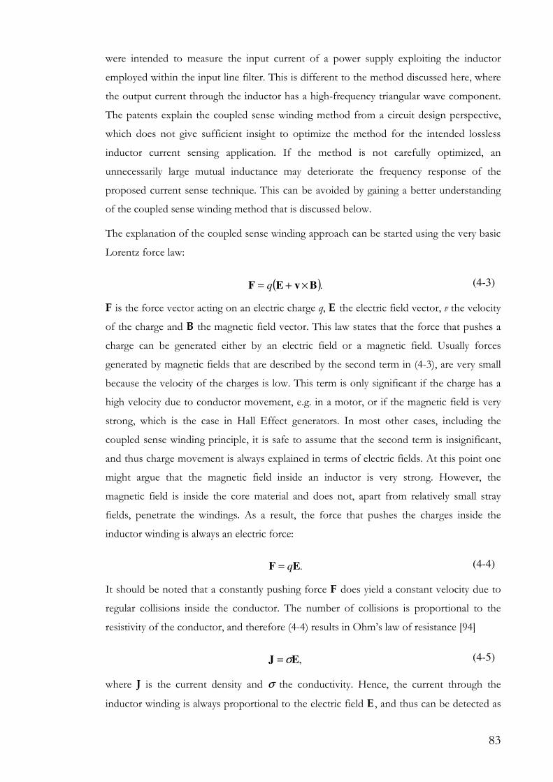
83
were intended to measure the input current of a power supply exploiting the inductor
employed within the input line filter. This is different to the method discussed here, where
the output current through the inductor has a high-frequency triangular wave component.
The patents explain the coupled sense winding method from a circuit design perspective,
which does not give sufficient insight to optimize the method for the intended lossless
inductor current sensing application. If the method is not carefully optimized, an
unnecessarily large mutual inductance may deteriorate the frequency response of the
proposed current sense technique. This can be avoided by gaining a better understanding
of the coupled sense winding method that is discussed below.
The explanation of the coupled sense winding approach can be started using the very basic
Lorentz force law:
( ).BvEF ×+= q (4-3)
F is the force vector acting on an electric charge q, E the electric field vector, v the velocity
of the charge and B the magnetic field vector. This law states that the force that pushes a
charge can be generated either by an electric field or a magnetic field. Usually forces
generated by magnetic fields that are described by the second term in (4-3), are very small
because the velocity of the charges is low. This term is only significant if the charge has a
high velocity due to conductor movement, e.g. in a motor, or if the magnetic field is very
strong, which is the case in Hall Effect generators. In most other cases, including the
coupled sense winding principle, it is safe to assume that the second term is insignificant,
and thus charge movement is always explained in terms of electric fields. At this point one
might argue that the magnetic field inside an inductor is very strong. However, the
magnetic field is inside the core material and does not, apart from relatively small stray
fields, penetrate the windings. As a result, the force that pushes the charges inside the
inductor winding is always an electric force:
.EF q= (4-4)
It should be noted that a constantly pushing force F does yield a constant velocity due to
regular collisions inside the conductor. The number of collisions is proportional to the
resistivity of the conductor, and therefore (4-4) results in Ohm’s law of resistance [94]
,EJ σ= (4-5)
where J is the current density and σ the conductivity. Hence, the current through the
inductor winding is always proportional to the electric field E , and thus can be detected as
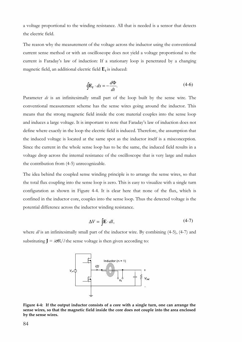
84
a voltage proportional to the winding resistance. All that is needed is a sensor that detects
the electric field.
The reason why the measurement of the voltage across the inductor using the conventional
current sense method or with an oscilloscope does not yield a voltage proportional to the
current is Faraday’s law of induction: If a stationary loop is penetrated by a changing
magnetic field, an additional electric field E f is induced:
.∫Φ
−=⋅dt
ddsfE
(4-6)
Parameter ds is an infinitesimally small part of the loop built by the sense wire. The
conventional measurement scheme has the sense wires going around the inductor. This
means that the strong magnetic field inside the core material couples into the sense loop
and induces a large voltage. It is important to note that Faraday’s law of induction does not
define where exactly in the loop the electric field is induced. Therefore, the assumption that
the induced voltage is located at the same spot as the inductor itself is a misconception.
Since the current in the whole sense loop has to be the same, the induced field results in a
voltage drop across the internal resistance of the oscilloscope that is very large and makes
the contribution from (4-5) unrecognizable.
The idea behind the coupled sense winding principle is to arrange the sense wires, so that
the total flux coupling into the sense loop is zero. This is easy to visualize with a single turn
configuration as shown in Figure 4-4. It is clear here that none of the flux, which is
confined in the inductor core, couples into the sense loop. Thus the detected voltage is the
potential difference across the inductor winding resistance.
∫ ⋅=∆ ,dlV E
(4-7)
where dl is an infinitesimally small part of the inductor wire. By combining (4-5), (4-7) and
substituting J = iσR/l the sense voltage is then given according to:
Figure 4-4: If the output inductor consists of a core with a single turn, one can arrange the sense wires, so that the magnetic field inside the core does not couple into the area enclosed by the sense wires.

85
RiVvs =∆=
(4-8)
As a result it can be said that the model in Figure 4-3 is incorrect since the coupled sense
winding principle does not work by inducing a counteracting voltage but rather by avoiding
any induced voltages at all. Therefore the model shown in Figure 4-5a can be derived. It
should be noted that there is a magnetic field surrounding the inductor wire due to the
flowing current i(t) that penetrates the loop built by the sense wires (Figure 4-5a). This
behaviour can be embedded into the model as a mutual inductance M in series to the
winding resistance R (Figure 4-5b). The mutual inductance is significantly smaller than the
inductance L. During a hardware experiment a mutual inductance M that was 160 times
smaller than L was measured. Although the voltage induced due to the mutual inductance
M is much smaller than with the conventional method, it still significantly disturbs the
measurement of the voltage across R. To solve this problem a low-pass filter can again be
used to filter out this induced voltage as shown in Figure 4-5b. However, it should be
noted that since the magnitude of the faraday component is two orders of magnitude
smaller than with the conventional method, the corner frequency of the low-pass filter is
now much higher as shown in Figure 4-2. Due to this improvement any over- or
undercompensation that might occur due to a mismatched low pass filter occurs at a much
higher frequency, and thus allows excellent waveform fidelity up to much higher
frequencies.
As a result one can draw the conclusion that the parasitic inductance seen by the sense
wires is not given by the self-inductance of the inductor but by the mutual inductance
between the sense and main loop. Consequently, it is important to make sure that the area
enclosed by the sense loop is as small as possible. What this means in practise is
demonstrated in Figure 4-6 for an inductor with multiple turns. For an optimized design, it
is essential that the sense winding is arranged parallel to the main winding in order to
Figure 4-5: a) A more precise model for the coupled sense winding method. b) The magnetic field due to i(t) that couples into the sense loop can be modelled as a mutual inductance M. The low-pass filter then filters out any induced voltages due to M.

86
reduce the area enclosed by the sense wires.
It is feasible to wind the sense winding of the coupled sense winding method independent
of the main winding. However, the resulting area enclosed by the sense wire will almost
always be larger compared with that of the optimized design shown in Figure 4-6. As a
result, the mutual inductance is increased, which means that the corner frequency is
unnecessarily deteriorated. Another reason to reduce the area enclosed by the sense wires is
the effect of any external stray magnetic fields. These fields may couple into this area and
induce a signal that has nothing to do with the current flowing through the main winding.
These disturbances cannot be compensated with a low-pass filter. However, if the area
enclosed by the sense windings is small then the signal will be small. For the conventional
method, external magnetic fields couple into the sense wire that encloses the magnetic
core. For an inductor with one turn as shown in Figure 4-4, this means that the area
enclosed by the sense winding is at least the size of the core cross sectional area. Moreover,
the stray field through the sense loop of the conventional method is amplified by the
permeability of the core material.
4.3 Experimental Results
The configuration of the DC-DC buck converter circuit is depicted in TABLE I. The
current through the inductor, L, takes the form of a triangular current waveform on a
larger DC current, shown in Figure 4-7. Using the conventional method without a low pass
filter (R1 = 0 and C1 = 0), the sense voltage vs is given by the sum of Faraday’s induction
law and voltage drop across the winding resistance:
Figure 4-6: For an inductor with multiple turns, the sense wire has to be located parallel and as close as possible to the main winding, with the intention that the area enclosed by the sense wire is as small as possible.
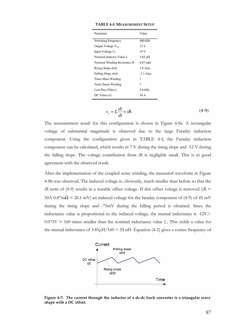
87
.iRdt
diLvs += (4-9)
The measurement result for this configuration is shown in Figure 4-8a. A rectangular
voltage of substantial magnitude is observed due to the large Faraday induction
component. Using the configuration given in TABLE 4-I, the Faraday induction
component can be calculated, which results in 7 V during the rising slope and -12 V during
the falling slope. The voltage contribution from iR is negligible small. This is in good
agreement with the observed result.
After the implementation of the coupled sense winding, the measured waveform in Figure
4-8b was observed. The induced voltage is, obviously, much smaller than before so that the
iR term of (4-9) results in a notable offset voltage. If this offset voltage is removed (iR =
30A0.87mΩ = 26.1 mV) an induced voltage for the faraday component of (4-9) of 45 mV
during the rising slope and -75mV during the falling period is obtained. Since the
inductance value is proportional to the induced voltage, the mutual inductance is -12V/-
0.075V ≈ 160 times smaller than the nominal inductance value L. This yields a value for
the mutual inductance of 3.85µH/160 = 24 nH. Equation (4-2) gives a corner frequency of
TABLE 4-I: MEASUREMENT SETUP
Parameter Value
Switching Frequency 400 kHz
Output Voltage Vout 12 V
Input Voltage Vin 19 V
Nominal Inductor Value L 3.85 µH
Nominal Winding Resistance R 0.87 mΩ
Rising Slope di/dt 1.8 A/µs
Falling Slope di/dt -3.1 A/µs
Turns Main Winding 7
Turns Sense Winding 7
Low-Pass Filter fc 5.8 kHz
DC Value i(t) 30 A
Figure 4-7: The current through the inductor of a dc-dc buck converter is a triangular wave shape with a DC offset.

88
5.8 kHz for the coupled sense winding method with 0.87 mΩ winding resistance. This is a
significant improvement over the 36 Hz corner frequency of the bare inductor.
In the measurement shown in Figure 4-8c a low-pass filter has been applied with a cut-off
frequency of 5.8 kHz in order to compensate the mutual inductance. It should be noted
that the higher corner frequency allows for the use of smaller capacitors. Large capacitors
generally come at higher cost and provide poorer high frequency performance. As the
measurement confirms, the low-pass filter corrects the frequency response above 5.8 kHz,
reproducing the current waveform through the inductor. In addition the coupled sense
winding method is not affected by variations in the performance of the inductor core
material, and thus shows no dependence on temperature of the core or DC offset current
unlike the conventional method.
The frequency responses of the conventional and coupled sense winding method have
been examined by forcing a square wave current with a frequency of 125 Hz through the
inductor. The conventional method uses a low-pass filter that has been matched to the
nominal inductor and winding resistance values depicted in TABLE I. To demonstrate the
superior waveform fidelity of the coupled sense winding technique even under mismatched
a)
-15
-10
-5
0
5
10
15
0 2 4 6 8 10
Time [us]
Ind
uc
tor
Vo
lta
ge
[V
]
b)
-150
-100
-50
0
50
100
150
0 2 4 6 8 10
Time [us]
Se
ns
e V
olt
ag
e [
mV
]
c)
0
5
10
15
20
25
30
35
0 2 4 6 8 10
Time [us]
Fil
tere
d S
en
se
Vo
lta
ge
[m
V]
Figure 4-8: Measurement of the inductor voltage with a DC output current of 30 A. a) Conventional approach without compensation filter. b) Proposed approach using a sense winding. c) Proposed approach combined with a low-pass filter having a cut-off frequency of 5.8 kHz.

89
conditions, the corner frequency of the low-pass filter connected to the coupled sense
winding has been designed at 8.8 kHz, so that an undercompensation above 5.8 kHz is
seen. The measurement results are shown in Figure 4-9. They clearly demonstrate a
significant improvement in waveform fidelity for the coupled sense winding (Figure 4-9b)
over the conventional approach (Figure 4-9a).
With a corner frequency in the kHz regime the coupled sense winding method may even be
competitive with a shunt resistor. A shunt resistor can be modelled with a mutual
inductance connected in series to a resistance. In the experimental setup, a shunt resistor of
300 µΩ was employed to measure the output current. This resistor yielded an
experimentally verified corner frequency of 20 kHz. However, the shunt resistor introduces
a power loss of 1 Watt, and provides an output voltage three times smaller than the
coupled sense winding technique described here. The small voltage drop from the shunt
resistor complicates the amplification due to the limited gain-bandwidth-product of
amplifiers. On the other hand, the shunt resistor does provide much lower thermal drift,
and has tighter initial tolerance than the coupled sense winding approach.
4.4 Summary
The presented coupled sense winding method does substantially enhance the waveform
fidelity of the conventional lossless inductor current sense technique by increasing the
apparent corner frequency of the inductor. The resulting current sense signal is undistorted
up to several kilohertz compared with the conventional method where the signal is already
a)
0
5
10
15
20
25
30
0 2 4 6 8 10
Time [ms]
Ind
uc
tor
Vo
lta
ge
[m
V]
b)
0
5
10
15
20
25
30
0 2 4 6 8 10
Time [ms]
Ind
uc
tor
Vo
lta
ge
[m
V]
Figure 4-9: Comparison of the waveform fidelity between the conventional and proposed method using a 125 Hz square wave current that has been forced through the inductor. a) Due to the low corner frequency of the conventional method, the sense voltage is notable distorted. b) The proposed method allows excellent waveform fidelity up to 5.8 kHz and thus gives an accurate representation of the 125 Hz square waveform.

90
distorted around ten hertz. This fits well for current controlled DC-DC converters that
usually have the zero crossing of the closed control loop in the kilohertz regime. The
improvement is achieved with a sense winding, having equal number of turns to the main
winding. The mutual inductance of the sense winding is reduced to more than two orders
of magnitudes smaller than the self-inductance by means of minimizing the area enclosed
by the sense wires. Other advantages are:
• The mutual inductance is temperature stable and independent of the DC offset
current through the inductor.
• Increased immunity against magnetic stray fields
• The low-pass filter requires a significant smaller capacitor, and thus provides lower
cost and better high frequency behaviour.
• No additional power losses
• Large output voltage amplitude
It has been shown that the dynamic performance of the proposed lossless output inductor
current method approaches that of the copper trace current sense method and the shunt
resistor. The winding resistance of the inductor will exhibit the same thermal drift as a
copper trace since the winding normally consists out of copper. This means it is feasible to
implement a similar temperature correction. However, the inductor winding resistance
provides significant higher voltage drop than a copper trace, and thus notably simplifies the
amplification stage. This means that the achievable measurement bandwidth at a given cost
budget will be substantially higher than with the copper trace current sense approach. It
also has been demonstrated during the investigation of the copper trace current sense
approach that the skin effect is small compared with mutual inductance effects since the
reactance increases linearly with frequency while the skin effect increases only with the
square root. For these reasons, the output inductor current sense method is even more
attractive for current sensing in power converters than the copper trace approach.

91
Chapter 5
A Simple and Accurate Transformer Based Current Sensor
5.1 Introduction
The previous two chapters have introduced the copper trace and output inductor current
sensing techniques, which exploit Ohm’s law of resistance. These reliable and simple
current sensing principles measure high direct currents at fair accuracy and low cost, and
thus provide an attractive solution to measure the output current of power converters with
DC output. However, a shortcoming of the proposed techniques is the lack of electrical
isolation and moderate measurement bandwidth, which make it difficult to measure
currents with high frequency content or currents on high voltage potentials that occur in
the PFC power conversion stage (Chapter 1). This chapter investigates a current sensing
principle based on Faraday’s law of induction that provides high measurement bandwidth
and electrical isolation at low cost.
Current transformers (CT) provide exceptional performance in terms of accuracy, thermal
drift, electrical isolation, measurement bandwidth and cost. These properties come about
through the use of inexpensive magnetic core materials and an extremely simple and robust
working principle. Unfortunately, the CT is unable to measure direct currents, which is why
high-performance current sensors are usually constructed by combining a CT with a DC
capable sensing principle that exhibits fair measurement bandwidth like fluxgates and Hall
Effect sensors. However, the combination of two sensing principles is expensive and
results in bulky current sensors.
In Appendix I, a circuit is shown that allowed the use a CT to measure direct currents by
periodically saturating the core material (Figure A-3). This circuit was extensively used in
the thirties and later replaced by the Hall Effect technology that enabled the construction

92
of DC current sensors at smaller size and larger measurement bandwidth. In the meantime,
several authors presented improved circuit variants [55-57, 103], with the circuit proposed
by Severns at APEC in 1986 probably being the simplest [88]. This circuit has the potential
to allow high-bandwidth current measurement at the low cost, high accuracy and high
robustness of a CT. So far, this circuit has been ignored by industry and academia, possibly
due to the combination of its unconventional working principle and the inability of the
proposed circuit to measure currents down to zero. No practical implementations have
been found and an extensive literature review did not unearth any related publications.
Although the proposed circuit is simple, the control scheme is difficult to implement in
analogue circuit technology and favours the use of microcontrollers. However, at the time
the circuit was invented microcontrollers were too expensive to build a cost-effective
current sensor. Naturally, this has changed in the last few decades. In this chapter, the
development of this circuit using a microcontroller is studied. Several modifications are
proposed in order to allow the measurement of currents down to zero, which eliminates
the only remaining problem to build a commercial successful current senor.
5.2 The Circuit Proposed by Severns
A known problem of the transformer based DC current sensor presented in Appendix I
(Figure A-3) is the large number of secondary turns necessary to reduce the power loss in
the sense resistor, which made the circuit large and expensive. The power loss of this
circuit, ignoring core losses, is then given according to:
.s
pv
N
iP ≈ (5-1)
It can be seen that for a given primary current ip the power loss is determined by the
number of secondary turns N and the sense voltage vs.
The circuit presented fifty years later by Severns uses only one transformer and forces the
core into the linear mode for a small amount of time. The excitation voltage that drives the
base of transformer Q1 (Figure 5-1) has a square wave shape with small duty cycle. A low
duty cycle D enables the use of a smaller winding ratio since the current through the sense
resistor Rs is then flowing just for a short amount of time. The power loss of the circuit
proposed by Severns is [88]:
.s
pv
N
iDP ≈ (5-2)

93
This technique results in a much smaller and less costly current sensor that is able to sense
DC currents whilst providing electrical isolation. However, the reduction in complexity
comes at the cost of an inability to measure negative currents [53].
The detailed working principle of the circuit proposed by Severns (Figure 5-1) can be
explained using the basic current transformer equation that was derived in Chapter 2 using
Faraday’s law of induction:
( ).
0
2 ∫ −=⋅−=t
m
p
t
r
mp
s iN
idtv
HAN
l
N
ii
µµ (5-3)
N is the number of secondary turns, A the core cross sectional area, and vt the secondary
transformer winding voltage. The second term in (5-3) is known as the magnetising current
im. It should be noted that the relative permeability µr of the core material is a function of
the applied H field similar to fluxgates. However, in a simplified B-H loop model only two
operating modes are distinguished: In the linear region, the core has a high relative
permeability µr, whilst in the saturated state the relative permeability is one and the core
behaves like free space (Figure 5-2a). It should be noted that in the saturated mode (5-3) is
only valid if the secondary winding density is constant and the primary conductor is
centred in the transformer core that has the shape of a toroid. Otherwise, the H field in the
core depends on the position of the primary conductor and the working principle cannot
be adequately described with (5-3).
Before t = 0 it is assumed that the core is saturated by a large DC primary current ip, and
switch Q1 is open (Figure 5-3). Accordingly, the secondary current is is zero and (5-3)
becomes:
Rs
Q1
Vdc
Sample & Hold
ip
D1
D2
N : 1is
vt
+
-
vs
+
-
Figure 5-1: Proposed DC current sensor by Severns at APEC 1986 [88].

94
( ).0)0(
,0)0(
m
p
s
iN
i
i
=
=
(5-4)
Therefore, the magnetising current im at t = 0 is solely given by the primary current. Switch
Q1 is then closed at t = 0 and a voltage vt is applied across the secondary winding that
generates a magnetic field that counteracts the field aroused by the primary current and
leads to a decreasing magnetising current:
( ) ,00
2
⋅−−= ∫
t
tm
m
p
s dtvAN
li
N
ii
µ (5-5)
( ) .00
2 ∫ ⋅−=t
tm
mm dtvAN
lii
µ (5-6)
As a result, the magnetising current im decreases quickly since the relative permeability of
the saturated core is just one (Figure 5-2b), and the secondary current is starts to rise
(Figure 5-3). After time t1 has elapsed, the core enters its linear mode since the magnetising
current falls below the saturation level Hsat of the core material:
( ) .1N
lHti msat
m = (5-7)
The time t1 can now be calculated by substituting (5-4) and (5-7) into (5-6):
( ).
0 1
00
2 ∫ ⋅−=
t
tmpmsat dtvAN
l
N
i
N
lH
µ (5-8)
Figure 5-2: A simple approximate B-H loop of a magnetic core material.
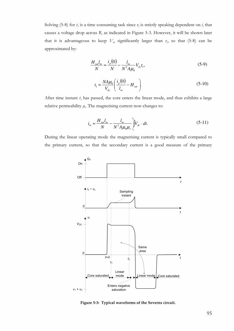
95
Solving (5-8) for t1 is a time consuming task since vt is strictly speaking dependent on is that
causes a voltage drop across Rs as indicated in Figure 5-3. However, it will be shown later
that it is advantageous to keep Vdc significantly larger than vs, so that (5-8) can be
approximated by:
( ),
01
0
2tV
AN
l
N
i
N
lHdc
mpmsat
µ−≈ (5-9)
( ).
00
1
−≈ sat
m
p
dc
Hl
i
V
NAt
µ (5-10)
After time instant t1 has passed, the core enters the linear mode, and thus exhibits a large
relative permeability µr. The magnetising current now changes to:
.2
10
2 ∫ ⋅−≈
t
t
dc
r
mmsatm dtV
AN
l
N
lHi
µµ (5-11)
During the linear operating mode the magnetising current is typically small compared to
the primary current, so that the secondary current is a good measure of the primary
vt
t
0
VDC
t
0
is ~ vs
Q1
On
Off
v1 + v2
Sampling
instant
Same
area
t
t2t=0
Core saturated
Linear
mode
Enters negative
saturation
Core saturatedLinear mode
t1
Figure 5-3: Typical waveforms of the Severns circuit.

96
current. In a first approximation, the secondary current is given according to (ip/N >> im):
.N
ii
N
ii
p
m
p
s ≈−= (5-12)
As a result, the secondary current is proportional to the primary current as long as the core
is in the linear mode (Figure 5-3). Similar to the current transformer, the magnetising
current causes a measurement error that can be minimised by using a core with large
relative permeability. It should be noted that since the magnetising current is decreasing the
secondary current in the Severns circuit shows an inverse droop effect.
In general, the secondary current can be used to measure the primary current until the
transformer reaches its negative saturation level after time t2 has elapsed (Figure 5-2), and
the magnetising current starts to decrease quickly. According to (5-3) the secondary current
will then start to increase, and the voltage drop across Rs becomes significant compared
with Vdc (Figure 5-3). For this reason, the on-time of Q1 has to be chosen, so that under all
operating conditions the core never enters negative saturation. The time interval t2 - t1
during which the secondary current is a good measure of the primary current is given
according to:
( ) .2
,
12
0
2
0
2
2
1
N
lHttV
AN
l
dtVAN
l
N
lH
N
lH
msatdc
r
m
t
t
dc
r
mmsatmsat
≈−
⋅−≈− ∫
µµ
µµ (5-13)
.2 012
dc
rsat
V
NAHtt
µµ≈− (5-14)
The circuit proposed by Severns does exploit the fact that time interval t2 - t1 is longer than
t1 as it is illustrated in (Figure 5-2b). As a result, the on-time of switch Q1 can be
dimensioned, so that the transformer core is in the linear mode at the end of the on-time of
switch Q1 under all measurement conditions. A valid current sample is then acquired by
sampling the voltage drop across the shunt resistor Rs. The on-time of switch Q1 in Figure
5-3 is shown longer than theoretically necessary to illustrate the behaviour if the core enters
negative saturation. In practise, the sampling instant will be chosen in order to minimise
the on-time of Q1, to reduce the power loss and to maximise the possible sampling
frequency. However, for zero primary current, the maximum on-time of switch Q1 is
reduced to 1/2(t2 - t1). The minimum on-time of Q1, on the other hand, is determined by
t1,max at the maximum primary current ip,max:
97
( )
.
,2
1
max,00
max,112
−>
>−
sat
m
p
dcdc
rsat Hl
i
V
NA
V
NAH
ttt
µµµ (5-15)
( ) .1
,
max,
max,
m
p
rsat
sat
m
p
rsat
l
iH
Hl
iH
>+
−>
µ
µ
(5-16)
Since µr >> 1:
.max,
m
p
rsatl
iH >µ (5-17)
This condition can also be expressed in terms of the saturation flux density Bsat that is
usually given in the core datasheet:
0
max,
0max,
0max,
0
,
,
µ
µ
µµµ
msatp
m
p
sat
m
p
rsat
lBi
l
iB
l
iH
<
>
>
(5-18)
Equation (5-18) indicates that the maximum primary current is given by the saturation flux
density and geometry of the core material. For an exemplary 9/6/3 toroid core with
magnetic path length of 23 mm and a ferrite material that has a typical saturation flux
density of 300 mT, the maximum measurable primary current is 5.5 kA. It will be shown
later that in practise this measurement range is severely reduced if the primary current is
not centred inside the toroid core, which means that the assumptions made for (5-3) are
not valid anymore.
After the current sample has been acquired, switch Q1 is opened and the diodes D1 and D2
(Figure 5-1) allow the secondary current to freewheel until the initial operating state is
retrieved where the magnetising current overtakes the full primary current. The original
circuit proposed by Severns employed a low-pass filter instead of a sample-and-hold circuit
to average the sense voltage across Rs. At that time, this circuit was used to reduce the
system cost but has the disadvantage that the linearity is altered due to switching noise.
Today, inexpensive microcontrollers with integrated analogue-to-digital converter and
sample-and-hold circuits are available that make the use of a low-pass filter obsolete. The

98
microcontroller can also synthesise the control signal for Q1, which further reduces the
circuit complexity and cost.
5.2.1 Limitations of the Severns Circuit
In order to achieve high measurement accuracy a high relative permeability is essential to
reduce errors caused by the magnetising current. For this reason, Severns proposed the use
of core materials with rectangular B-H loop characteristic that exhibit an extremely high
relative permeability beyond 100,000. An exemplary B-H loop with resulting magnetising
current is given in Figure 5-4. An important advantage over the previous core characteristic
is that the magnetising current during time interval t1 to t2 is almost constant. Moreover, the
magnetising current during this time interval is negative, which means that for zero primary
current a small but positive offset current results according to (5-3). This is advantageous
for the circuit that samples the sense voltage across Rs because negative voltages always
cause problems.
Obviously, an important characteristic of this kind of B-H loop is the coercive force Hc
that determines the magnetisation current. For current sensors with fair accuracy
requirements, this magnetisation current can be ignored. However, if very high accuracy
sensors are required the magnetisation current can be considered as a constant offset
current. Amorphous and nanocrystalline cores are available with extremely low coercive
force and low thermal drift that enable the construction of highly accurate current sensors.
It will be shown later that since the coercive force of amorphous and nanocrystalline
magnetic cores can be specified to ±15%, it is not necessary to calibrate the magnetising
current during the production process and a correction constant can be permanently
H ~ im
B
-Bsat
+Bsat
µ0
µ0µr
µ0
t = t2
+Hc-Hc
a)
t
t = 0
t2
ip(0)/N
t1
imb)
t = 0
t = t1
Figure 5-4: Magnetic core material with rectangular B-H loop.
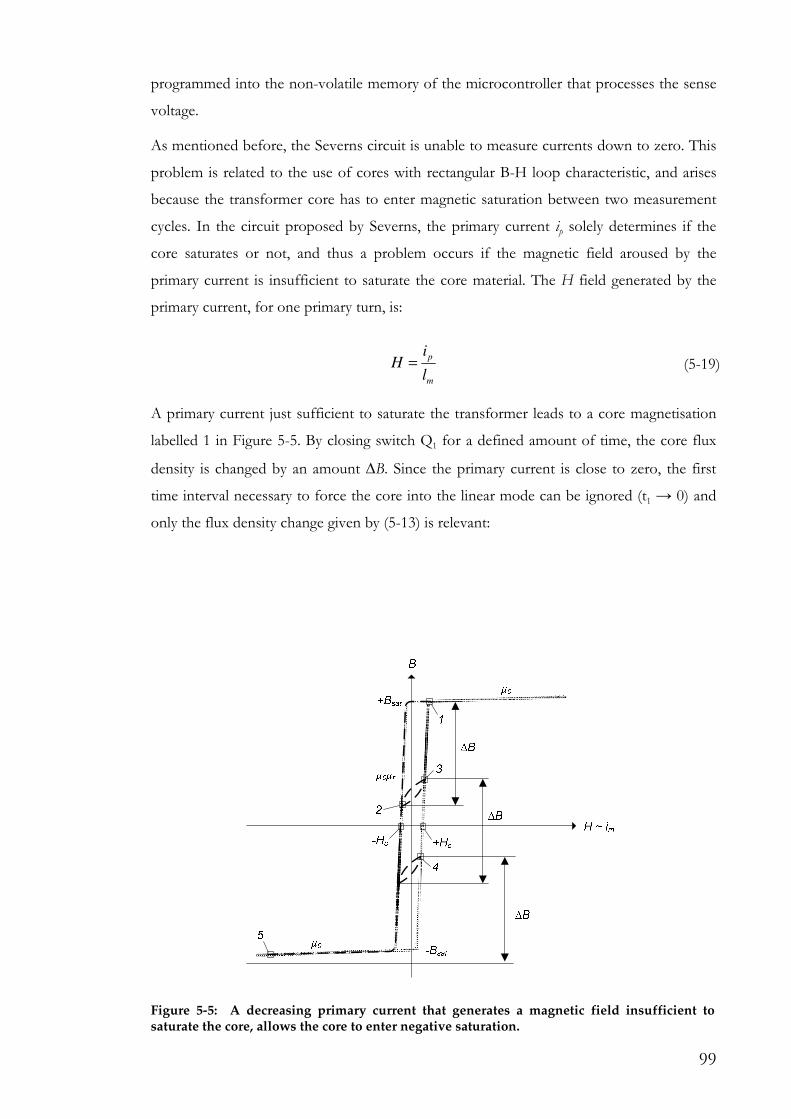
99
programmed into the non-volatile memory of the microcontroller that processes the sense
voltage.
As mentioned before, the Severns circuit is unable to measure currents down to zero. This
problem is related to the use of cores with rectangular B-H loop characteristic, and arises
because the transformer core has to enter magnetic saturation between two measurement
cycles. In the circuit proposed by Severns, the primary current ip solely determines if the
core saturates or not, and thus a problem occurs if the magnetic field aroused by the
primary current is insufficient to saturate the core material. The H field generated by the
primary current, for one primary turn, is:
m
p
l
iH = (5-19)
A primary current just sufficient to saturate the transformer leads to a core magnetisation
labelled 1 in Figure 5-5. By closing switch Q1 for a defined amount of time, the core flux
density is changed by an amount ∆B. Since the primary current is close to zero, the first
time interval necessary to force the core into the linear mode can be ignored (t1 → 0) and
only the flux density change given by (5-13) is relevant:
Figure 5-5: A decreasing primary current that generates a magnetic field insufficient to saturate the core, allows the core to enter negative saturation.

100
.
,
2
2
tNA
VB
V
BNAt
dc
dc
≈∆
∆≈
(5-20)
The secondary current is then sampled at position 2 in Figure 5-5 and switch Q1 opened
immediately. However, in the current scenario it is assumed that the primary current
decreased in the meantime and the resulting H field sets the core magnetisation to position
3. The core now stays at position 3 until the next sampling cycle drives the core
magnetisation again closer to the negative saturation of the core material. If the primary
current is still steadily decreasing, the primary current may force the core magnetisation to
rest at position 4 between the sampling intervals. The next time the sampling switch Q1 is
closed, the core will be driven into negative saturation shown as position 5, which means
that the secondary current is significantly altered by the magnetising current and not useful
as a current sample of the primary current anymore. The transfer function between the
sampled voltage across Rs and the primary current that has been experimentally derived by
Severns is depicted in Figure 5-6. It demonstrates that at small primary currents the sense
voltage starts to increase since the core reaches negative saturation. Unfortunately, it is
impossible for the processing electronics to decide if the primary current is below the
minimum allowed value just by observing the sense voltage.
For this reason, the circuit proposed by Severns fails to measure primary currents that
generate a magnetic field smaller than the coercive force of the core material. Therefore:
Figure 5-6: The circuit proposed by Severns is unable to measure small current [88].
101
,HH c < (5-21)
,m
p
cl
iH < (5-22)
.cmp Hli > (5-23)
According to (5-23), core properties like lm and Hc determine the minimum measurable
primary current ip. However, the magnetic path length lm does not provide a lot of freedom,
since this value is given by the minimum core window area necessary to hold the primary
and secondary winding. The coercive force Hc, finally, is a material parameter and not
adjustable. Overall, the limitation not being able to measure currents down to zero is a
serious limitation of the circuit proposed by Severns especially since the processing
electronics is unable to detect if the voltage across Rs is invalid due to low primary currents.
5.3 Circuit Modifications that Extend the Measurement Range
Although the circuit invented by Severns has many desirable characteristics like electrical
isolation, low complexity, low power loss, high bandwidth and large output signal
amplitude, the inability to measure currents down to zero severely limits the usefulness of
this current sensing technique. Not only can low currents not be measured, but they
generate an output voltage that appears to represent a high primary current. Overall, this
current sensor can only be considered if the primary current never falls below the
minimum allowed value, or an additional measurement enables the sensor to decide if the
measurement is reliable or not. One important contribution of this thesis is the description
of a solution for this problem that was presented for the first time at the Australasian
Universities Power Engineering Conference [53].
5.3.1 Constant Auxiliary Current
The simplest solution to extend the measureable current range is to add an auxiliary
winding with the same polarity as the primary winding to the Severns circuit (Figure 5-7).
The current through the auxiliary winding ia generates a magnetic field in the same
direction as the field generated by the primary current. The H field within the core during
the time the core material is saturated is then given by:
( ),1aapp
mm
aa
m
ppiNiN
ll
iN
l
iNH +=+= (5-24)

102
where Na is the number of auxiliary turns and ia the auxiliary current. To make the
following considerations more general, the number of primary turns is not necessarily one
anymore and given by Np. This equation is again only valid if the generated magnetic field
in the toroid core is homogenous, which demands that the winding density of the auxiliary
and primary winding has to be constant. For just one primary turn, this means that the
conductor has to be centred inside the toroid core. Using (5-21), the magnitude of the
auxiliary current ia can be determined at a primary current ip = 0, so that the core material
does not run into negative saturation:
( )
.
,0
m
aac
pc
l
iNH
iHH
<
=<
(5-25)
Equation (5-25) provides a design rule to prohibit the magnetic core material to reach
negative saturation. Solving for ia:
.a
mca
N
lHi > (5-26)
To reduce power losses due to the auxiliary current, its value is chosen only slightly higher
than Hclm/Na, so that (5-26) is valid over the whole operating range. A simple resistor in
series to the power supply voltage Vdc can provide the auxiliary current ia, which is
demonstrated in Figure 5-7 with R1. When the transformer core is saturated, the voltage
across the auxiliary winding Na is zero, and thus:
Rs
Q1
Vdc
D2
D1
Microcontroller
A/D
with S/H
R1
ipNs : Np
Na
ipvt
saturable core
with square B-H
characteristic
vs
+
-
+
-
ia
Figure 5-7: By adding an auxiliary winding with constant current to the Severns circuit it becomes feasible to measure currents down to zero.

103
.1R
Vi dca = (5-27)
It is interesting to note that this circuit can theoretically also sense negative currents if
larger values are chosen for ia.
In Figure 5-7 the sample and hold circuit has been replaced by a digital-signal-processor
(DSP) with integrated analogue-to-digital converter (ADC). This configuration is designed
for use with digitally controlled power converters, where the current has to be sampled
once per switching cycle. Alternatively, a continuous analogue output signal can be
achieved by connecting a digital-to-analogue converter (DAC) to the DSP or by means of a
discrete sample-and-hold circuit.
Circuit Theory
A mathematical model is developed here to give a better understanding of the current
sensor behaviour. However, a useful theoretical treatment of this circuit is only possible by
making certain simplifications. The most important simplification is that the core material’s
B-H loop is treated as being rectangular, and thus µr is infinitively large. As a result, the
magnetising current is constant during the time the core material is in the linear mode.
Moreover, switches have zero on-resistance and diodes exhibit constant forward voltage.
Hardware experiments will later confirm that the model based on these simplifications is in
good accordance with the real circuit behaviour.
The proposed circuit with constant auxiliary current has three basic switching states: First
state is if Q1 is open and the core saturated. In switching state two, Q1 is closed and the
transformer forced into the linear mode. At the end of switching state two, the voltage
across the resistor Rs is sampled. Immediately afterwards, Q1 is opened and the transformer
magnetisation is forced back into the saturated state, which is called switching state three.
Of primary interest is the second switching state since it incorporates the sampling
procedure that determines the transfer function between primary current and sense voltage.
For the second switching state, an equivalent circuit diagram that is referenced to the
secondary side can be developed as shown in Figure 5-8.
Applying these conditions, the magnetising current im during second switching state is given
according to:
.s
mcm
N
lHi = (5-28)

104
By using Norton’s equivalent circuit theorem, the voltage sources Vdc and Vdc/na (Figure
5-8) can be converted into current sources, which yields the equivalent circuit diagram
shown in Figure 5-9. This circuit diagram is now used to determine the transfer ratio
between the primary current ip and the voltage drop across the sense resistor vs. According
to Kirchhoff the sum of all currents in Figure 5-9 at node 1 is zero:
.011
1
2
1
s
dcp
dcaam
s R
Vni
R
Vn
R
vni
R
v−++++= (5-29)
Solving for v1:
.1
1
21
1
R
n
R
R
Vnnii
R
V
va
s
dcapm
s
dc
+
−−−
= (5-30)
Using v1, the current trough the sense resistor is can be computed:
( ).1
11 vV
RR
v
R
Vi dc
sss
dcs −=−= (5-31)
The sense voltage vs then is:
.11
1
1
2
1
2
1
1 p
a
s
a
s
m
s
adc
dcdcsss i
R
n
R
n
R
n
R
iRR
nV
VvVRiv
+
+
+
+
−
+=−== (5-32)
Apparently, the transfer function vs = f(ip) is a linear function. Hence, (5-32) can be
partitioned into gain and offset. The gain m is:
Figure 5-8: Equivalent circuit diagram of the modified Severns circuit during the second switching state.

105
,2
1
1
sa
s
p
s
RnR
RRn
di
dvm
+== (5-33)
which is the parallel connection of R1/na2 and Rs. The offset v0 is given by:
( ) ( ).
10
1
2
1
10
+
+
+=== m
adca
sa
sps i
R
nVn
RnR
RRivv (5-34)
The offset voltage is the sum of the magnetising current im and the current flowing through
R1/na2 referred to the secondary side multiplied by the parallel connection of R1/na
2 and Rs.
For the special case of na = 1, the following formulas result:
( )
( ) .1
,2
1
1
1
11
10
s
s
p
sa
mdc
s
sa
RR
RRn
di
dvnm
iR
V
RR
RRnv
+===
+
+==
(5-35)
The offset voltage v0 defined in (5-35) gives an interesting insight into the circuit behaviour.
Assuming that ia is usually set only slightly larger than im, the auxiliary current ia can be
approximated by:
.ma ii ≈ (5-36)
As mentioned above, the magnetising current im is constant during the linear mode of the
core material since the B-H loop can be simplified by assuming infinitely large relative
permeability µr. The offset voltage v0 for the special case na = 1 can now be written by
combining (5-27), (5-35) and (5-36) as:
( ) ( ) .3211
1
1
10
RR
RRiii
RR
RRnv
s
smmm
s
sa
+=+
+== (5-37)
It is now interesting to compare this result with the original Severns circuit. Unfortunately,
Severns did not include a small signal model in his paper presented at APEC’86 but one
Figure 5-9: Equivalent circuit diagram of the modified Severns circuit after applying Norton’s equivalent circuit theorem.

106
can obtain this model easily by setting the auxiliary current ia inside the equivalent circuit
diagram (Figure 5-9) to zero. Obviously, this can be achieved by setting R1 to ∞, and thus
(5-35) changes to:
( )
( ) .
,
1
10
s
p
s
sm
nRdi
dvRm
RiRv
==∞=
=∞=
(5-38)
By comparing the equations for the original Severns circuit (5-38) with the modified
version that has a third winding (5-35), it can be observed that for the modified circuit the
gain m has become the parallel connection between Rs and R1. Therefore, the apparent
sense resistance Ra of the modified circuit is:
.2
1
1
sa
sa
RnR
RRR
−= (5-39)
For the Severns circuit the sense resistor value is equal to the apparent sense resistor (Rs =
Ra), whilst for the modified circuit with a third winding and na = 1 the sense resistor value
for a given apparent resistance can be calculated according to:
.1
1
a
as
RR
RRR
−= (5-40)
If the sense resistor value Rs is chosen, so that the resulting apparent sense resistance yields
the same gain as the original circuit proposed by Severns, (5-37) indicates that the offset
voltage v0 of the modified circuit is three times larger. Another disadvantage of this
modified circuit is the direct relation between supply voltage Vdc and offset voltage v0. This
is undesirable since then the measurement accuracy becomes dependent on the stability of
the supply voltage Vdc.
An experimental prototype with constant auxiliary current (TABLE 5-I) yielded the
transfer function depicted in Figure 5-10. The magnetising current has been determined
prior to the measurement of the transfer function using a hardware experiment. The
measured transfer function confirms that a constant auxiliary current enables the
measurement of primary currents down to zero. However, a large offset voltage is present
that may make it difficult to acquire the sense voltage using an analogue-to-digital
converter. The calculated curve has been generated using (5-35) and is in good agreement
with the measurement results. Hence, the model provides a reasonable representation of
the real circuit behaviour despite the simplifications made at the start.

107
Constant Auxiliary Current Provided by a High-Impedance Current Source
Since the high offset voltage and the direct influence of the supply voltage on the sense
voltage is not desirable, the auxiliary current can be alternatively provided by a current
source with high internal impedance as shown in Figure 5-11. The resulting equivalent
circuit diagram is shown in Figure 5-12. The sum of all currents at node 1 then changes to:
.0 1
s
dcpaam
s R
Vniini
R
v−+++= (5-41)
Following the same procedure as before, the sense voltage vs becomes:
.spsaasms RniRinRiv ++= (5-42)
Accordingly, the offset voltage v0 and the gain m are:
TABLE 5-I: MEASUREMENT SETUP FOR PROTOTYPE WITH CONSTANT AUXILIARY CURRENT
Parameter Value
Supply Voltage Vdc 12 V
Sampling Frequency 100 kHz
Auxiliary Resistor R1 680 Ω
Magnetising Current im 13.5 mA
Sense Resistor Rs 68 Ω
Primary Winding Np 1 T, AWG 18
Secondary Winding Ns 50 T, AWG 30
Auxiliary Winding Na 50 T, AWG 30
Core Material Ferroxcube 3R1 (Ferrite)
Core Size (OD/ID/HT) 9/6/3 mm
2.0
3.0
4.0
5.0
6.0
7.0
8.0
0.0 0.5 1.0 1.5 2.0 2.5 3.0 3.5
i p [A]
vs [
V]
-1
-0.5
0
0.5
1
Ab
so
lute
Err
or
[%]
Experimental Results
Calculated
Absolute Error
Figure 5-10: Experimental results of the modified Severns circuit with constant auxiliary current. This circuit is now able to measure currents down to zero but exhibits a large offset voltage.

108
( )
.
,0
s
maas
nRm
iinRv
=
+= (5-43)
For the case na = 1:
( )
sa
amsa
nRnm
iiRnv
==
+==
)1(
)1(0 (5-44)
After applying the definition (5-36), the offset voltage v0 can be written as:
( ) ( ) .210 msmmsa iRiiRnv =+== (5-45)
Obviously, the offset voltage is only twice that of the original circuit proposed by Severns,
and exhibits less offset than the circuit that provides the auxiliary current by means of a
series resistor R1. An additional benefit is that the offset voltage is independent of the
Figure 5-11: The auxiliary current ia can be provided by a high-impedance current source to reduce the offset voltage and to eliminate the dependence on the supply voltage.
Figure 5-12: The equivalent circuit diagram of the modified Severns circuit by generating the auxiliary current with a high impedance current source.

109
supply voltage. However, the auxiliary current directly influences the measurement
accuracy and has to be provided with sufficient precision, which yields higher cost
compared to the previously discussed solution.
5.3.2 Pulsed Auxiliary Current
So far it has been demonstrated that the Severns circuit can be supplemented with a third
winding to extend the measurement range down to zero. Apart from the necessary
additional transformer winding, the bias current produces a steady power drain, and
furthermore produces an increased offset voltage at the sense resistor. To achieve high
accuracy, high precision control of the current through the bias winding is required, which
does increase the cost. It is possible to overcome these shortcomings using a slightly more
complex circuit.
The inability to measure small primary currents is a distinct disadvantage of the original
Severns circuit, and occurs because the transformer core is not properly saturated before
the sampling cycle. However, there is no need to use a constant auxiliary current, and the
same goal can be achieved by using a pulsed current that is held to zero during the
Rs
Vdc
D2
D1
Microcontroller R1
Np : Ns
Na
vt
saturable core
with square B-H
characteristic
vs
Q2
ia
Q1
A/D
with S/H
ip
ip
is
+
-
+
-
Figure 5-13: Proposed circuit with pulsed auxiliary current.

110
sampling interval (Q1 = on). Figure 5-13 depicts the proposed circuit in which the auxiliary
winding Na is adapted to force selectively the magnetic core into saturation. In this circuit,
a saturating switch Q2 is pulsed closed under the control of a microcontroller. When the
saturating switch is closed, current ia flows from power source Vdc through the auxiliary
winding Na. The magnitude of current ia is limited to Vdc/R1, and chosen according to
(5-26) to assure that the magnetic core is brought into saturation prior to the measurement
of the primary current ip. It should be noted that when the saturating switch Q2 is open, no
current flows through the auxiliary winding and therefore no power is dissipated during the
off cycle.
The working principle can be explained as follows: If the primary current is zero, the H
field in the core after switch Q1 is opened is zero, and the core magnetisation reaches
position 1 in Figure 5-14. The saturating switch Q2 is then closed to saturate the core by a
magnetic field that is given according to (5-24). The selection of the auxiliary current
according to (5-26) will assure that the core will be saturated even at zero primary current
(Position 2, Figure 5-14). It should be noted that if the primary current ip was insufficient
by itself to hold the core in saturation before the closure of the saturating switch Q2, the
current ia will not immediately rise to Vdc/R1, and a transitory negative voltage will appear
across the secondary winding. Therefore, the on-time of switch Q2 has to be chosen long
enough for ia to rise to its steady-state level, at which time the magnetic core is saturated. In
a practical circuit there will be some leakage inductance in series to the auxiliary winding
that may slow down the rising rate of the auxiliary current ia after switch Q2 is closed.
However, the leakage inductance of a reasonable transformer design is only 1−2 % of the
inductance of the auxiliary winding itself, and therefore there is no noticeable increase of
the minimum on-time of switch Q2. Once the core is saturated, the saturating switch Q2 is
opened, and the core magnetisation moves to Position 3 in Figure 5-14. Soon afterwards,
the sampling switch Q1 is closed, forcing the core material into the linear mode (Position
4), in which the sense voltage vs, representing the primary current ip, is measured.
The auxiliary current is only necessary at small currents in order to avoid negative
saturation of the core as explained in above. Also it has been demonstrated that it takes
several cycles, depending on the values of Bsat and ∆B, until the core material finally reaches
negative saturation. This behaviour can be exploited by initially disabling the auxiliary
switch, and activate it as soon as the sense voltage, which is proportional to the primary
current, falls below a certain threshold level that is given by (5-23). This helps to reduce
the power consumption since the auxiliary current is then only activated at very small
primary currents.

111
An important advantage over the constant auxiliary current is that the secondary current
during the sampling instant does not depend at all on the auxiliary current ia. Accordingly,
the transfer function of this circuit is the same as for the original Severn’s circuit:
.
,0
s
sm
nRm
Riv
=
= (5-46)
The proposed current sensor has the same desirable characteristics as the original Severns
circuit, which means that the measurement accuracy is independent of the supply voltage
and solely determined by the core characteristics. Moreover, this circuit is able to measure
currents down to zero. An exemplary transfer function of this type of current sensor
(TABLE 5-II) is shown in Figure 5-15. It can be seen that the offset voltage is notably
H ~ im
B
-Bsat
+Bsat
µ0
µ0µr
µ0
+Hc-Hc
2
4
1
3
Figure 5-14: The auxiliary switch ensures that the core magnetisation is set back to point 2 under all measurement conditions, and therefore enables the measurement of currents down to zero.
TABLE 5-II: MEASUREMENT SETUP PROTOTYPE WITH PULSED AUXILIARY CURRENT
Parameter Value
Supply Voltage Vdc 12 V
Sampling Frequency 200 kHz
Auxiliary Resistor R1 1 kΩ
Magnetising Current im 2.7 mA
Sense Resistor Rs 10 Ω
Primary Winding Np 1 T, AWG 18
Secondary Winding Ns 51 T, AWG 30
Auxiliary Winding Na 51 T, AWG 30
Core Material VAC 6025Z (Amorphous)
Core Size (OD/ID/HT) 11.2/5.1/5.9 mm
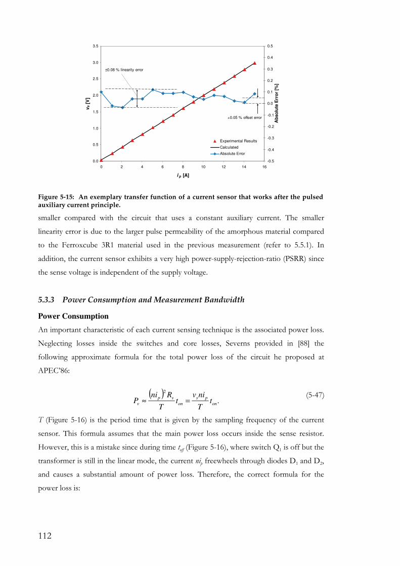
112
smaller compared with the circuit that uses a constant auxiliary current. The smaller
linearity error is due to the larger pulse permeability of the amorphous material compared
to the Ferroxcube 3R1 material used in the previous measurement (refer to 5.5.1). In
addition, the current sensor exhibits a very high power-supply-rejection-ratio (PSRR) since
the sense voltage is independent of the supply voltage.
5.3.3 Power Consumption and Measurement Bandwidth
Power Consumption
An important characteristic of each current sensing technique is the associated power loss.
Neglecting losses inside the switches and core losses, Severns provided in [88] the
following approximate formula for the total power loss of the circuit he proposed at
APEC’86:
( ).
2
on
ps
on
sp
v tT
nivt
T
RniP =≈
(5-47)
T (Figure 5-16) is the period time that is given by the sampling frequency of the current
sensor. This formula assumes that the main power loss occurs inside the sense resistor.
However, this is a mistake since during time toff (Figure 5-16), where switch Q1 is off but the
transformer is still in the linear mode, the current nip freewheels through diodes D1 and D2,
and causes a substantial amount of power loss. Therefore, the correct formula for the
power loss is:
0.0
0.5
1.0
1.5
2.0
2.5
3.0
3.5
0 2 4 6 8 10 12 14 16
i p [A]
vs [
V]
-0.5
-0.4
-0.3
-0.2
-0.1
0.0
0.1
0.2
0.3
0.4
0.5
Ab
so
lute
Err
or
[%]
Experimental Results
Calculated
Absolute Error
±0.08 % linearity error
+0.05 % offset error
Figure 5-15: An exemplary transfer function of a current sensor that works after the pulsed auxiliary current principle.

113
( ).
21
T
tvvnitnivP
offponps
v
++≈
(5-48)
The voltages v1 and v2 are the voltage drops across diodes D1 and D2. The time toff is defined
by the time required to reset the core magnetisation to the saturated state. As it has been
explained in Chapter 2 for the current transformer, Faraday’s law of induction requires the
mean voltage vt across the secondary transformer winding to be zero. Accordingly, the time
toff can be described according to (Figure 5-16):
( ) ( )
( )( )
.
,
21
21
onsdc
off
offonsdc
tvv
vVt
tvvtvV
+
−=
+=−
(5-49)
Inserting the result into (5-48) yields:
.on
pdc
v tT
niVP ≈
(5-50)
Comparing this result with (5-47) shows that the additional power loss is substantial,
especially since vs is usually much smaller than Vdc. An additional problem is that most of
vt
t
ton
0
VDC
t
0
is
Q1
On
Off
v1 + v2
Sampling
instant
Same
area
t
toff
T
Figure 5-16: Timing diagram of the proposed current sensor.

114
the power loss occurs inside the zenerdiode D1, which makes it difficult to dissipate the
generated heat. Often a zenerdiode with high power rating may be necessary that comes in
a bulky package with low thermal resistance in order to be able to dissipate the heat, and
this increases the cost for the current sensor.
For the proposed circuit with constant auxiliary current (Figure 5-7), the power loss inside
the resistor R1 connected to the auxiliary winding also contributes to the total power loss,
which can be calculated according to:
.1
2
,R
VP dc
auxv = (5-51)
Since the power loss caused by the auxiliary current increases with the square of the supply
voltage Vdc, it is attractive to connect R1 to a power supply other than Vdc that has a smaller
output voltage. For the circuit that uses a current source to generate the auxiliary current
(Figure 5-11), the power loss is determined by the circuit that implements the current
source functionality.
In the circuit that employs a pulsed auxiliary current (Figure 5-13), the auxiliary current
only flows for a short amount of time that is necessary to properly saturate the core.
Moreover, the auxiliary current is only required at small primary currents ip insufficient to
properly saturate the magnetic core material. In practise, this means that for primary
currents sufficient to saturate the core switch Q2 can remain open, and no power is
dissipated in R1. Switch Q2 only needs to be activated for currents close to zero, and thus
the overall power loss that occurs in R1 is negligible small compared with the total power
loss, and can be neglected in the specification of the maximum power loss of the current
sensor.
Instead of dissipating a lot of power in the zenerdiode D1 during time interval toff, it is
feasible to recover the energy by modifying the proposed circuit with pulsed auxiliary
current as shown in Figure 5-17. During the time interval toff, the current is then
freewheeling through diode D1 and the voltage source Vdc. Apart from the negligible power
loss due to the voltage drop across diode D1, no energy is dissipated during toff. The
zenerdiode across the secondary winding can be omitted, which reduces the system cost
and components count. This technique is also applicable to the previously discussed circuit
with constant auxiliary current but is not discussed here. The total power dissipation of the
current sensor then becomes:

115
,T
tvniP on
spv ≈ (5-52)
which is the power loss originally predicted by Severns. The drawback of this extension is
that the time required to force the core back into saturation becomes dependent on the
supply voltage Vdc and the number of auxiliary turns Na, and cannot be adjusted simply by
selecting the appropriate zenerdiode. However, this is a small price to pay, compared with
the benefit of large power savings of usually more than 50%. An alternative would be to
connect the auxiliary winding to a power supply other than Vdc.
The result of (5-52) can be expressed in terms of measurement bandwidth Bw that
according to the sampling theorem is half the sampling rate fs:
.2
1
2
1
TfB sw ==
(5-53)
Combining (5-52) and (5-53) yields:
.2 onspwv tvniBP ≈ (5-54)
The on-time ton is determined by the time required to force the magnetic core material from
the saturated into the linear state. This change in the magnetic flux density ∆B is given by
Rs
Vdc
Microcontroller
Np : Ns
Na
vt
saturable core
with square B-H
characteristic
vs
Q2
ia
Q1
A/D
with S/H
ipis
R1
D1
v2
+
-
+
-
Figure 5-17: Proposed circuit with pulsed auxiliary current and energy recycling.
116
the on-time ton and can be calculated according to:
.1
0
∫ ⋅=∆ont
t
s
dtvAN
B (5-55)
It has been mentioned before that the secondary winding voltage can be approximated by
the supply voltage Vdc since for an optimal design Vdc should be notably larger than vs.
Moreover, vs reaches its final value not before the end of time interval ton. Using this
approximation one obtains:
.
,
dc
son
s
ondc
V
ABNt
AN
tVB
∆≈
≈∆
(5-56)
The minimum necessary flux density change necessary to force the core into the linear
mode is a function of the primary current. Since the proposed circuit uses a constant on-
time ton for switch Q1, the maximum flux density change has to be considered, which occurs
at the maximum primary current:
.max,
0max
+=∆ c
m
ppH
l
NiB µ (5-57)
Since the coercive force is usually much smaller than the magnetic field generated by the
primary current (5-57) can be approximated by:
.max,
0max
m
pp
l
NiB µ≈∆ (5-58)
The combination of (5-54), (5-56) and (5-58) then yields:
.2 02
max,
≈
m
ppp
dc
swv
l
ANii
V
vBP
µ (5-59)
It can be seen that it is disadvantageous to have multiple primary turns, and thus most
circuits will be designed for Np = 1. Moreover, the maximum power loss occurs at the
maximum primary current, so that (5-59) can be written as:
.2 02
max,max,
≈
m
p
dc
swv
l
Ai
V
vBP
µ (5-60)
With this result, it becomes possible to optimise the sensor performance for a specific
application. There is a trade-off to be made between bandwidth Bw, gain (here the
amplitude of vs), power loss Pv,max and the maximum current ip,max that can be measured. Due

117
to the direct proportionality between bandwidth and power loss, it will be attractive in
many applications to sacrifice bandwidth in order to reduce the power loss.
It is interesting to note that by reducing the cross sectional area A of the magnetic core
material the power loss is reduced. This change not only reduces the power loss in Rs but
also the size, price, and power loss of the transformer core. Equation (5-60) implies that
reducing A to zero is the best design for reduction in power loss. However, for permalloy
the limitation of the reduction in A has been described by Schwarze in [104]. He found
that at very low cross sectional areas the classical core loss theory is not valid anymore, and
the core losses start to increase if the area is reduced below a certain limit. Moreover, it will
be shown later that a small core volume is more susceptible to external magnetic noise.
Measurement Bandwidth
It should be noted that there exists a theoretical limit for the maximum bandwidth Bw,max
that is determined by:
( ).
2
1
2
1
,
min
max,
min
offon
w
offon
ttTB
ttT
+==
+=
(5-61)
Combining (5-49), (5-56), and (5-58) yields:
( )( )
.
1221
max,0
max,
+
−+
≈
vv
vVANNi
VlB
sdcspp
dcmw
µ
(5-62)
For the embodiment that takes advantage of energy recycling the expression v1 + v2 has to
be replaced by Vdc / na:
.
112 max,0
max,
−+
≈
dc
saspp
dcmw
V
vnANNi
VlB
µ
(5-63)
It can be seen that the maximum theoretical measurement bandwidth is inversely
proportional to the maximum primary current. This result confirms again the finding that a
trade-off has to be made between bandwidth, maximum primary current, gain and power
loss. Equation (5-63) further implies that the cross sectional area A of the core material
should be made very small in order to increase the bandwidth. However, it has been
pointed out before that other physical phenomena make it impossible to reduce the cross
sectional area below a certain limit.
Summary

118
Equations (5-60), (5-62) and (5-63) describe the theoretical limit of this current sensing
principle for ideal switches, diodes and rectangular B-H loop characteristic of the core
material. In practise, however, the minimum on-time of switch Q1 will be notably larger
than indicated by (5-56), mainly because the switch needs a substantial amount of time to
change the switching state and the core material’s B-H loop is not perfectly rectangular.
These circumstances do reduce the maximum possible bandwidth and increase the power
loss of the current sensor. Another limitation that is discussed later is the position of the
primary conductor, which should be centred inside the toroid core.
5.3.4 Comparison
TABLE 5-III provides an overview of the modified circuits. Generally, the performance
increases with higher circuit complexity. However, it should be noted that the auxiliary
switch necessary to achieve a pulsed auxiliary current has low power requirements, and thus
the additional cost and size is small.
5.4 Electrical Isolated Voltage Sensor
The discussed current sensor can also be used as an electrical isolated voltage sensor by
employing a series resistor at the primary side that converts the voltage into a current. This
current can then be measured by means of the proposed current sensor. However, the
following theoretical analysis will point out important differences between using the circuit
for voltage and current sensing. In this analysis, the current sensor with pulsed auxiliary
TABLE 5-III: COMPARISON OF THE THEORETICAL PERFORMANCE
Original Severns Circuit Constant auxiliary current provided by a resistor
Constant auxiliary current provided by a high
impedance current source
Pulsed auxiliary current with energy
recycling
Power Loss
on
pdct
T
niV
1
2
R
Vt
T
niVdc
on
pdc+
1
2
R
Vt
T
niVdc
on
pdc+
T
tvni onsp
Offset msiR ( )
+
+
+m
adca
sa
s iR
nVn
RnR
RR
1
2
1
1 1 ( )maas iinR + msiR
Gain snR
sa
s
RnR
RRn
2
1
1
+ snR snR
Range
0µmsat
p
s
mc lBi
N
lH<<
0
0µ
msatp
lBi <<
0
0µ
msatp
lBi <<
0
0µ
msatp
lBi <<
Switches 1 1 1 2
Diodes 2 2 2 1
Windings 2 3 3 3
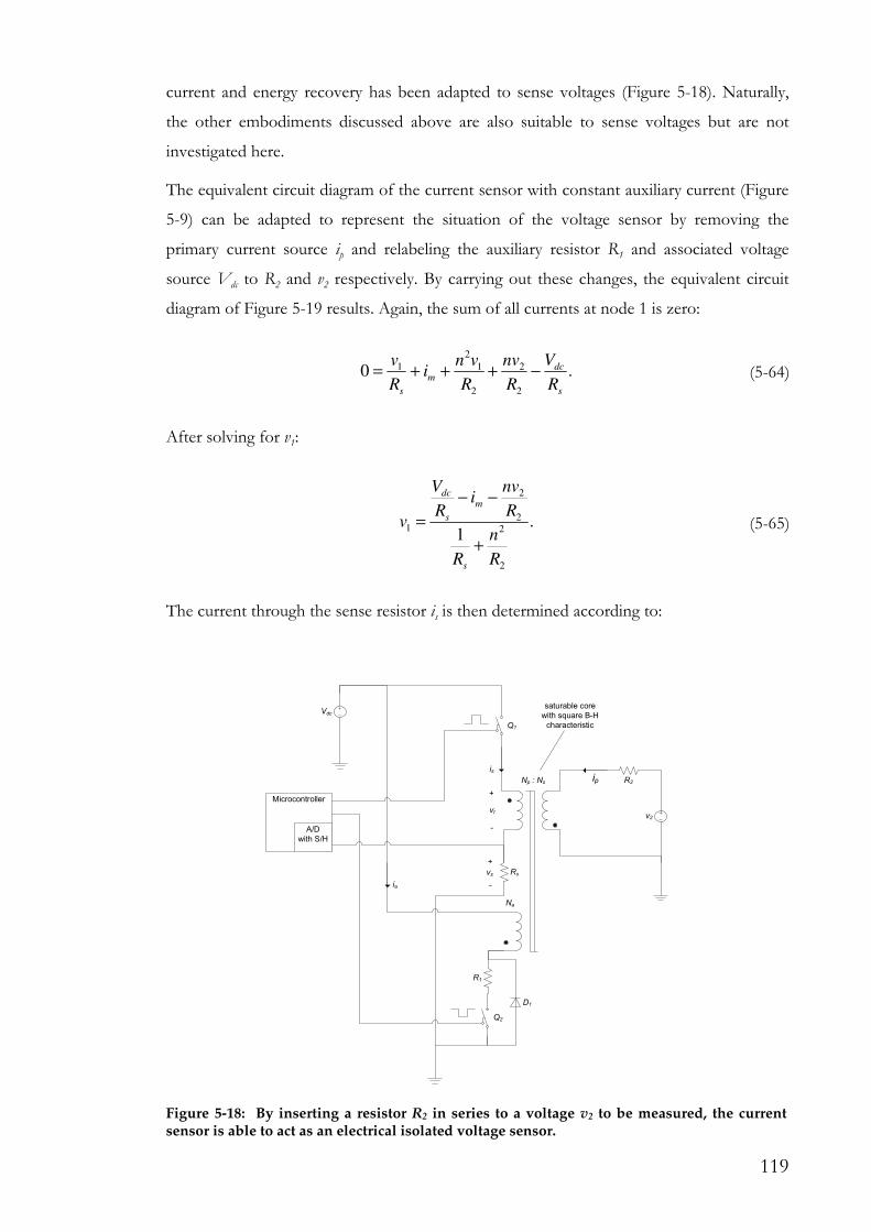
119
current and energy recovery has been adapted to sense voltages (Figure 5-18). Naturally,
the other embodiments discussed above are also suitable to sense voltages but are not
investigated here.
The equivalent circuit diagram of the current sensor with constant auxiliary current (Figure
5-9) can be adapted to represent the situation of the voltage sensor by removing the
primary current source ip and relabeling the auxiliary resistor R1 and associated voltage
source Vdc to R2 and v2 respectively. By carrying out these changes, the equivalent circuit
diagram of Figure 5-19 results. Again, the sum of all currents at node 1 is zero:
.02
2
2
1
2
1
s
dcm
s R
V
R
nv
R
vni
R
v−+++= (5-64)
After solving for v1:
.1
2
22
2
1
R
n
R
R
nvi
R
V
v
s
m
s
dc
+
−−
= (5-65)
The current through the sense resistor is is then determined according to:
Rs
Vdc
Microcontroller
Np : Ns
Na
vt
saturable core
with square B-H
characteristic
vs
Q2
ia
Q1
A/D
with S/H
ipis
R1
D1
v2
R2
+
-
+
-
Figure 5-18: By inserting a resistor R2 in series to a voltage v2 to be measured, the current sensor is able to act as an electrical isolated voltage sensor.

120
( ).1
11 vV
RR
v
R
Vi dc
sss
dcs −=−= (5-66)
By combining (5-65) and (5-66) the sense voltage vs is given by:
.1
2
22
2
1
R
n
R
iR
V
R
nv
VvVRiv
s
m
s
dc
dcdcsss
+
+−
+=−== (5-67)
Since the result is a linear function, (5-67) can be rearranged into gain and offset terms:
( ) .2
2
2
2
22
2
s
s
s
smdcs
RnR
Rnv
RnR
RRiVnv
++
++= (5-68)
Equation (5-68) indicates that the offset voltage is not only a function of the magnetising
current but also influenced by the supply voltage. The gain of this voltage sensor can then
be adjusted with resistors Rs and R2. However, a limiting factor is the power dissipation in
R2 (v22/R2) that determines the lower limit for R2. For high measurement accuracy and large
measurement range, the circuit should be dimensioned, so that:
.22
2nvRiVn mdc <<+ (5-69)
Inserting the definition for the magnetising (5-28) current yields:
.22 v
N
RlH
N
VN
p
mc
s
dcp<<+ (5-70)
In order to fulfil (5-70) the number of primary and secondary turns (Np, Ns) can be chosen
accordingly. If Vdc << v2 it is feasible to set Np = Ns, so that (5-68) simplifies to:
Figure 5-19: The Equivalent circuit diagram for the proposed isolated voltage sensor.
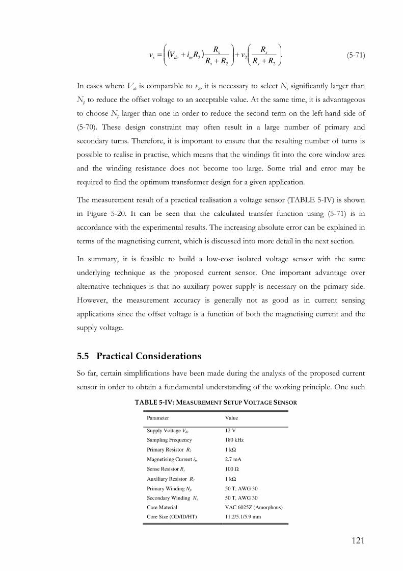
121
( ) .2
2
2
2
++
++=
RR
Rv
RR
RRiVv
s
s
s
smdcs (5-71)
In cases where Vdc is comparable to v2, it is necessary to select Ns significantly larger than
Np to reduce the offset voltage to an acceptable value. At the same time, it is advantageous
to choose Np larger than one in order to reduce the second term on the left-hand side of
(5-70). These design constraint may often result in a large number of primary and
secondary turns. Therefore, it is important to ensure that the resulting number of turns is
possible to realise in practise, which means that the windings fit into the core window area
and the winding resistance does not become too large. Some trial and error may be
required to find the optimum transformer design for a given application.
The measurement result of a practical realisation a voltage sensor (TABLE 5-IV) is shown
in Figure 5-20. It can be seen that the calculated transfer function using (5-71) is in
accordance with the experimental results. The increasing absolute error can be explained in
terms of the magnetising current, which is discussed into more detail in the next section.
In summary, it is feasible to build a low-cost isolated voltage sensor with the same
underlying technique as the proposed current sensor. One important advantage over
alternative techniques is that no auxiliary power supply is necessary on the primary side.
However, the measurement accuracy is generally not as good as in current sensing
applications since the offset voltage is a function of both the magnetising current and the
supply voltage.
5.5 Practical Considerations
So far, certain simplifications have been made during the analysis of the proposed current
sensor in order to obtain a fundamental understanding of the working principle. One such
TABLE 5-IV: MEASUREMENT SETUP VOLTAGE SENSOR
Parameter Value
Supply Voltage Vdc 12 V
Sampling Frequency 180 kHz
Primary Resistor R2 1 kΩ
Magnetising Current im 2.7 mA
Sense Resistor Rs 100 Ω
Auxiliary Resistor R1 1 kΩ
Primary Winding Np 50 T, AWG 30
Secondary Winding Ns 50 T, AWG 30
Core Material VAC 6025Z (Amorphous)
Core Size (OD/ID/HT) 11.2/5.1/5.9 mm

122
simplification was the assumption that the magnetising current of a core with rectangular
B-H loop characteristics is constant if the core is in the linear mode. However, a real
magnetic core material will exhibit finite relative permeability, which means that the
magnetising current becomes a function of time. Other non-ideal behaviour that needs to
be discussed is the influence of thermal drift, core loss and magnetic noise on the circuit
behaviour. These considerations will serve as a guide for the selection of the appropriate
core material to achieve the desired performance.
5.5.1 Linearity Error
The proposed current sensor has an output voltage that is proportional to the primary
current. For the circuit with pulsed auxiliary current the relationship is given by:
.spsms RniRiv += (5-72)
In this equation, the main contributor towards non-linear behaviour is the magnetising
current im. In the previous discussion, it was assumed that the employed core material had
an infinitely large relative permeability, which means that the magnetising current during
the linear mode is constant. Naturally, the relative permeability of a real core will never be
infinitive, and hence an investigation of the relationship between the relative permeability
and the measurement accuracy is required.
0.0
5.0
10.0
15.0
20.0
25.0
30.0
35.0
1.00 1.50 2.00 2.50 3.00 3.50 4.00 4.50
vs [V]
v2 [
V]
-1.0
-0.5
0.0
0.5
1.0
Ab
so
lute
Err
or
[%]
Experimental Results
Calculated
Absolute Error
Figure 5-20: Experimental results of the voltage sensor.

123
A distinct characteristic of the proposed isolated current sensor is its simplicity, which
allows it to keep the on-time of switch Q1 constant independent of the primary current.
Therefore, the on-time of Q1 has to be chosen in order to ensure that the core enters the
linear mode under all operational conditions. This circumstance is graphically explained
within Figure 5-21. At maximum primary current, the core magnetisation is at position ip,max.
After closing switch Q1, the core magnetisation is forced to position ip,0 by applying a
voltage across the secondary winding. The flux density change ∆B is given according to:
.1
0
dtvAN
Bont
t
s
⋅=∆ ∫ (5-73)
It is obvious that the on-time of switch Q1 determines the flux density change, and has to
be chosen so that the core reaches the linear mode. The minimum flux density change
∆Bmin necessary to force the core at the maximum primary current ip,max into the linear mode
is:
.0max,
min
m
pp
l
NiB
µ=∆ (5-74)
It has to be noted that until this point the core is still in the saturated mode and the relative
permeability equal to one (Figure 5-21). The on-time of switch Q1 is then given by:
( ) dtvVANl
Ni
BB
ont
sdc
sm
pp⋅−≤
∆≤∆
∫0
0max,
min
1
,
µ (5-75)
This inequality is not simple to solve since the sense voltage vs is a function of the primary
current ip and magnetising current im, and thus will result in a differential inequality.
Figure 5-21: B-H curve with finite relative permeability.

124
However, since the sense voltage is zero at t = 0, and by ignoring the magnetising current
the sense voltage is given by nip,maxRs at t = ton, the following approximation can be made:
.2
11max,
0max,
onspdc
sm
pptRniV
ANl
Ni
−≤
µ (5-76)
Therefore, the on-time is determined by:
.
2
1max,
0max,
−
≥
spdcm
spp
on
RiVl
ANNit
µ (5-77)
In order to reduce the power loss and increase the measurement bandwidth as discussed
before, ton should be as short as possible and is therefore chosen close to the minimum
allowed value.
If the primary current is zero, the core magnetisation before the closure of Q1 is set to
position ip,0 in Figure 5-21. After ton has elapsed, the flux density has then changed by an
amount of:
.
,1
0
0
0
AN
tVB
dtvAN
B
s
ondc
t
t
s
on
=∆
⋅=∆ ∫ (5-78)
At zero primary current the sense voltage vs is zero, and thus vt = Vdc. It should be noted
that if ton is chosen to reach ∆Bmin at maximum primary current, the final core magnetisation
after ton for maximum primary current is the starting point at zero primary current, which
means that there is a difference in the H field after ton has elapsed:
.
2
1
,
max,
max,
00
0
−
≈∆
=∆
=∆
spdcmr
dcpp
sr
ondc
r
RniVl
VNiH
AN
tVBH
µ
µµµµ
(5-79)
It can be shown that this equation is still valid even if ton has been chosen larger than the
minimum necessary value. The differential magnetising current ∆im is then given according
to:
.
2
1max,
max,
−
≈∆
=∆
spdc
dc
r
p
s
mm
RniV
Vni
N
Hli
µ (5-80)
The absolute measurement error then is:

125
.
2
12
1
2
1
max,max,
−
=∆
≈
spdc
dc
rp
m
RniV
V
ni
i
µε (5-81)
This result demonstrates why it is advantageous to keep the sense voltage vs = nipRs small
compared with Vdc. If nipRs << Vdc. (5-82) becomes:
.2
1
rµε ≈ (5-82)
An exemplary core material with µr = 100,000 results in a theoretical non-linearity of only
0.005 %. Hence, in order to obtain high measurement accuracy it is advantageous to select
a core material with large relative permeability, which is the reason why Severns proposed
the use of materials with rectangular B-H loop characteristics.
Equation (5-82) reveals a simple relation between measurement accuracy and relative
permeability of the core material. However, other non-ideal component properties like
voltage drop across switch Q1, switching delay of Q1, stray inductance of the transformer
and the winding resistance of the transformer have been ignored. These effects are
temperature dependent and do reduce the effective voltage drop vt across the secondary
winding. As a result, the rate of field change is reduced and the minimum on-time ton larger
than predicted by (5-77).
Position of the Primary Conductor
The position of the primary conductor and the winding density of secondary and auxiliary
winding will most likely be far away from the optimum, which means that the primary
conductor may not be centred in the toroid and the secondary and auxiliary winding
density may be uneven. Hardware experiments indicated that the position of the primary
conductor becomes increasingly important at large primary currents. Figure 5-22 illustrates
the magnetic fields around the primary conductor for the centred and non-centred case.
Since the core is saturated, the field is circular around the conductor. It can be clearly seen
that the magnetic field in the toroid is inhomogeneous for a non-centred primary
conductor (Figure 5-22b). After switch Q1 has been closed, a homogenous counteracting
field within the first toroid core is generated by means of the secondary winding (not
shown), and the resulting field is the superposition of the two fields. It is clear that for the
non-centred conductor (Figure 5-22b) at positions where the field generated by the primary
current is weak the counteracting field forces the core into the linear mode much earlier
than at locations where the primary field is stronger. It will then take a certain amount of
time until the whole toroid core is in the linear mode, and in a worst case scenario, the core

126
may enter negative saturation at certain location before all of the toroid reached the linear
mode. But even if this is not the case, the observed B-H loop changes then from a
rectangular shape to a shape depicted in Figure 5-23 (dashed line).
Instead of ∆Bmin the minimum necessary flux density change to force the core into the
linear mode is then given by ∆B as illustrated in Figure 5-23. As a result, it takes more time
to force the core into the linear mode and the differential magnetising current is notably
larger than indicated by (5-80). ∆B may be determined by means of a finite element
simulation program or measured using a hardware experiment. Once the minimum
required flux density change ∆B is known, the on-time can be approximated by:
,2
1
,1
max,
0
on
s
spdc
t
t
s
tAN
RniVB
dtvAN
Bon
−≈∆
⋅=∆ ∫ (5-83)
.
2
1max, spdc
son
RniV
ABNt
−
∆≈ (5-84)
At zero primary current, the flux density change ∆B0 is then:
.
2
1max,
0
spdc
dc
RniV
BVB
−
∆≈∆ (5-85)
The differential magnetising current ∆im can be calculated according to:
Primary ConductorToroid Core
Strong Magnetic
Field
Weak Magnetic
Field
a) b)
Magnetic Field
Lines
Figure 5-22: If the primary conductor is not centred inside the toroid core, the magnetic field will saturate the core material unevenly, and thus enlarge the time required to force the core out of saturation.

127
,
2
1max,
0spdc
dc
r RniV
VBH
−
∆≈∆
µµ (5-86)
.
2
1max,
0
−
∆≈∆
spdcs
dcm
r
m
RniVN
VlBi
µµ (5-87)
The absolute measurement error becomes then a function of the primary current:
.
2
12max,max,
0
−
∆≈
spdcpp
dcm
r RniVNi
VlB
µµε (5-88)
It should be noted that ∆B is a function of ip,max, and thus the conclusion that the absolute
error decreases with the maximum primary current may not be valid, especially if the core
starts to enter negative saturation. Again, if the sense voltage is significantly smaller than
the supply voltage (5-88) becomes:
.2 max,0 pp
m
r Ni
lB
µµε
∆≈ (5-89)
For an exemplary amorphous magnetic core with Np = 1, lm = 25.6 mm, ∆B = 100 mT, ip,max
= 15 A and µr = 100,000 a theoretical non-linearity of ±0.07 % results. The experimental
measurement shown in Figure 5-15 were made using this amorphous magnetic core and
yielded a non-linearity of ±0.08 %., which is in good agreement with the theory. Since the
3R1 material from Ferroxcube exhibits a significantly lower pulse permeability of around
20’000, the measured non-linearity as shown in Figure 5-10 is considerably larger than in
H ~ im
B
µ0
µ0µr
µ0
ip,max
∆Bip,0
∆B0
Figure 5-23: If the primary conductor causes a non-homogenous magnetic field in the toroid core, the core material’s B-H characteristic is altered due to local saturation phenomena.

128
Figure 5-15, as would be expected from theory.
Summary
In general, it can be said that the absolute measurement error is inverse proportional to the
relative permeability of the core material. This is the main motivation for the use of
materials with rectangular B-H loop characteristic that exhibit a relative permeability
beyond 100,000. At large primary currents it becomes increasingly important that the
primary conductor is centred inside the toroid core. Otherwise, not only the accuracy is
deteriorated but also the power loss and bandwidth deteriorate due to the longer on-time
required to force the core into the linear mode. In the extreme case, the sensing principle
may fail if the core partially enters negative saturation. This problem can by solved by
ensuring that the primary conductor is always centred inside the toroid core.
Another source of non-linear behaviour is the shunt resistor used to convert the secondary
current into a voltage, and the analogue-to-digital converter that samples the voltage across
the shunt resistor. The characteristics of these components can be found in the datasheet
of the manufacturer and is not part of this discussion. By carefully choosing sense resistor
and analogue-to-digital converter, the additional measurement errors can be kept very low.
5.5.2 Thermal Drift
Temperature stability is another important characteristic of a current sensor especially since
power converters are subject to large temperature variations. If a core material with very
high relative permeability is employed, the transfer function of the sensor with pulsed
auxiliary current is given according to:
.spsms RniRiv += (5-90)
Similar to the non-linear investigation, it can be said that the sense resistor Rs will only have
minor influence on the overall thermal drift since standard resistors with very low thermal
coefficients of less than 20 ppm/K are available. The magnetising current im for a magnetic
core with a large relative permeability can be approximated by:
.s
mcm
N
lHi ≈ (5-91)
Hc is the coercive force of the core with rectangular B-H characteristic, lm the magnetic path
length and Ns the number of secondary turns. As it has been demonstrated before, a core
with large relative permeability and centred primary conductor has a highly constant
magnetising current, and thus it can be assumed that the magnetising current is constant
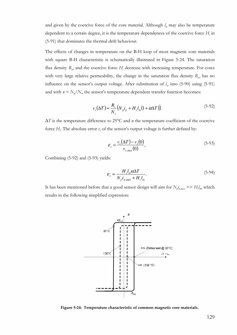
129
and given by the coercive force of the core material. Although lm may also be temperature
dependent to a certain degree, it is the temperature dependences of the coercive force Hc in
(5-91) that dominates the thermal drift behaviour.
The effects of changes in temperature on the B-H loop of most magnetic core materials
with square B-H characteristic is schematically illustrated in Figure 5-24. The saturation
flux density Bsat and the coercive force Hc decrease with increasing temperature. For cores
with very large relative permeability, the change in the saturation flux density Bsat has no
influence on the sensor’s output voltage. After substitution of im into (5-90) using (5-91)
and with n = Np/Ns, the sensor’s temperature dependent transfer function becomes:
( ) ( )( ).1 TlHiNN
RTv mcpp
s
ss ∆++≈∆ α (5-92)
∆T is the temperature difference to 25°C and α the temperature coefficient of the coercive
force Hc. The absolute error εs of the sensor’s output voltage is further defined by:
( ) ( )( )
,0
0
max,s
sss
v
vTv −∆=ε (5-93)
Combining (5-92) and (5-93) yields:
.max, mcpp
mcs
lHiN
TlH
+
∆≈
αε (5-94)
It has been mentioned before that a good sensor design will aim for Npip,max >> Hclm, which
results in the following simplified expression:
Figure 5-24: Temperature characteristic of common magnetic core materials.

130
.max,pp
mcs
iN
TlH ∆≈
αε (5-95)
Accordingly, the overall thermal drift is less if large primary currents are measured. As an
example, for a 15 A prototype current sensor with a single primary turn, an experimentally
derived coercive force Hc of 6.8 A/m, magnetic path length of 25.6 mm, temperature
coefficient α for Hc of -3000 ppm/K and ∆T = 100 °C an error εs of only 0.35 % results.
Accordingly, the apparent temperature coefficient αs of the prototype current sensor is 35
ppm/K:
.max,pp
mcs
iN
lH αα ≈ (5-96)
Experimental measurements of the thermal coefficients shown in Figure 2-25 give a value
of -25 ppm/K, similar to the predicted results. It should be noted that in this measurement
only the core was heated in order to exclude the influence of the sense resistor. The
apparent temperature coefficient can be even lower if larger current ip is being measured or
the number of primary turns Np increased. As an example, the temperature coefficient of a
220 A current sensor prototype (TABLE 5-V), with an approximate cost of 1 USD, at
maximum current was less than 5 ppm/K. In order to obtain separate numbers for gain
and offset drift, the transfer function of this prototype was measured six times at increasing
temperatures from -40°C to 130°C (Figure 5-25). Due to the very small drift, the initial
comment that the thermal drift of the sense resistor Rs is irrelevant to the overall thermal
drift of the sensor is no longer valid and great care need to be paid during the selection of
this resistor in order not to degrade the measurement accuracy.
TABLE 5-V: MEASUREMENT SETUP 220 A PROTOTYPE WITH PULSED AUXILIARY CURRENT
Parameter Value
Supply Voltage Vdc 12 V
Sampling Frequency 20 kHz
Auxiliary Resistor R1 1 kΩ
Magnetising Current im 1.5 mA
Sense Resistor Rs 1.7 Ω
Primary Winding Np 1 T, AWG 4
Secondary Winding Ns 138 T, AWG 28
Auxiliary Winding Na 85 T, AWG 30
Core Material Toshiba MT (Amorphous)
Core Size (OD/ID/HT) 22.8/12.8/6.6 mm
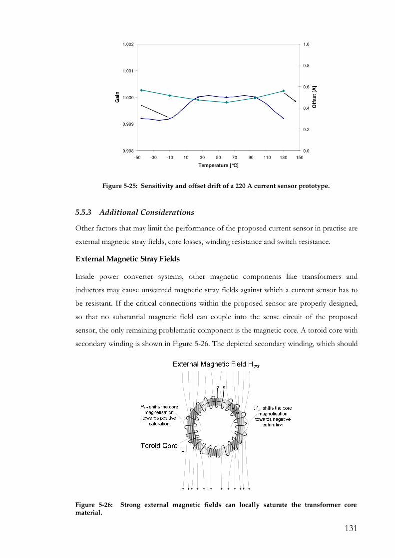
131
5.5.3 Additional Considerations
Other factors that may limit the performance of the proposed current sensor in practise are
external magnetic stray fields, core losses, winding resistance and switch resistance.
External Magnetic Stray Fields
Inside power converter systems, other magnetic components like transformers and
inductors may cause unwanted magnetic stray fields against which a current sensor has to
be resistant. If the critical connections within the proposed sensor are properly designed,
so that no substantial magnetic field can couple into the sense circuit of the proposed
sensor, the only remaining problematic component is the magnetic core. A toroid core with
secondary winding is shown in Figure 5-26. The depicted secondary winding, which should
0.998
0.999
1.000
1.001
1.002
-50 -30 -10 10 30 50 70 90 110 130 150
Temperature [°C]
Gain
0.0
0.2
0.4
0.6
0.8
1.0
Off
set
[A]
Figure 5-25: Sensitivity and offset drift of a 220 A current sensor prototype.
Figure 5-26: Strong external magnetic fields can locally saturate the transformer core material.
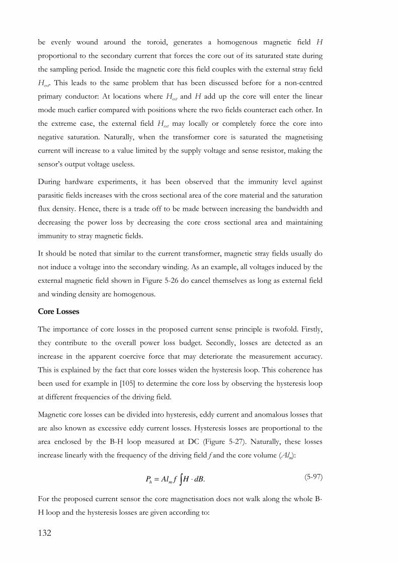
132
be evenly wound around the toroid, generates a homogenous magnetic field H
proportional to the secondary current that forces the core out of its saturated state during
the sampling period. Inside the magnetic core this field couples with the external stray field
Hext. This leads to the same problem that has been discussed before for a non-centred
primary conductor: At locations where Hext and H add up the core will enter the linear
mode much earlier compared with positions where the two fields counteract each other. In
the extreme case, the external field Hext may locally or completely force the core into
negative saturation. Naturally, when the transformer core is saturated the magnetising
current will increase to a value limited by the supply voltage and sense resistor, making the
sensor’s output voltage useless.
During hardware experiments, it has been observed that the immunity level against
parasitic fields increases with the cross sectional area of the core material and the saturation
flux density. Hence, there is a trade off to be made between increasing the bandwidth and
decreasing the power loss by decreasing the core cross sectional area and maintaining
immunity to stray magnetic fields.
It should be noted that similar to the current transformer, magnetic stray fields usually do
not induce a voltage into the secondary winding. As an example, all voltages induced by the
external magnetic field shown in Figure 5-26 do cancel themselves as long as external field
and winding density are homogenous.
Core Losses
The importance of core losses in the proposed current sense principle is twofold. Firstly,
they contribute to the overall power loss budget. Secondly, losses are detected as an
increase in the apparent coercive force that may deteriorate the measurement accuracy.
This is explained by the fact that core losses widen the hysteresis loop. This coherence has
been used for example in [105] to determine the core loss by observing the hysteresis loop
at different frequencies of the driving field.
Magnetic core losses can be divided into hysteresis, eddy current and anomalous losses that
are also known as excessive eddy current losses. Hysteresis losses are proportional to the
area enclosed by the B-H loop measured at DC (Figure 5-27). Naturally, these losses
increase linearly with the frequency of the driving field f and the core volume (Alm):
.∫ ⋅= dBHfAlP mh (5-97)
For the proposed current sensor the core magnetisation does not walk along the whole B-
H loop and the hysteresis losses are given according to:

133
.2 BHlAfP cmsh ∆= (5-98)
Hc is the coercive force, fs the sampling frequency and ∆B the flux density change that is at
maximum ∆B0 at zero primary current. It should be noted that this is a worst case
estimation for the hysteresis core loss since the magnetization after the main switch has
been opened will not immediately rise from –Hc to +Hc, which means that the area
enclosed by the actual B-H loop is reduced. An exemplary current sensor with amorphous
core material and Hc = 0.25 A/m, A = 5.1 mm2, lm = 25.6 mm, ∆B = 100 mT and fs = 100
kHz exhibits a worst-case hysteresis loss Ph of only 653 µW.
Magnetisation reversal at frequencies relevant to normal electrical circuits (below
microwave frequencies 109 Hz) is a thermally activated transition from a metastable to a
stable state. As such the process is time and rate dependent [106]. A number of authors
have shown by theory and hardware experiment that as the sweep rate dH/dt of the
magnetic field is increased there is an increase in the coercivity [107, 108]. In addition, fast
changing magnetic fields inside the magnetic core induce voltages into the core material
due to Faraday’s law of induction. These voltages lead to circulating currents in the core
material known as eddy currents, and thus generate losses that are inverse proportional to
the core material’s electrical resistance. It has been shown in [109, 110] that eddy currents
are generally small compared to anomalous and hysteresis loss since the resistance of ferrite
and amorphous materials is large and is further increased by skin effect at higher
frequencies. As mentioned before, it is possible to understand eddy current and anomalous
losses further in terms of a widening of the B-H loop as illustrated in Figure 5-27. As a
H ~ im
B
-Bsat
+Bsat
+Hc,a (100 kHz)
100 kHz
DC
+Hc (Datasheet @ DC)
Hysteresis loss
Eddy current and
anomalous loss
Figure 5-27: The coercive force given in the datasheet is often measured for DC excitation. At higher frequencies, anomalous and eddy current core losses yield an increased apparent coercive force.

134
result of this and the rate dependent coercivity, the apparent coercive force Hc,a for the
proposed current sense principle is often larger than indicated in the datasheet since the
coercive force is often specified at DC or low frequency driving fields. Since it is
notoriously difficult to derive the coercivity for a given driving field in the time domain, it
is necessary to determine this value by means of a hardware experiment. Such experiments
revealed that the apparent coercive force is definitely larger than given in the datasheet but
does not depend on the sampling frequency because the core is forced out of saturation by
applying a counteracting voltage across the secondary winding, which has an amplitude that
is independent of the sampling frequency. For the exemplary amorphous core with Hc =
0.25 A/m at DC, an apparent coercive force of 6.8 A/m has been measured. Therefore,
the total core losses Ph,e can be calculated using the apparent coercive force Hc,a:
.2 ,, BHlAfP acmseh ∆= (5-99)
Using the same configuration as above, the total core loss is 17.8 mW, and therefore it can
be said that anomalous losses are clearly more significant than hysteresis losses. However, it
should be noted that at maximum primary current the flux density change ∆B is reduced
for reasons mentioned before, which yields a core loss smaller than indicated by (5-99).
The above investigation did show that the apparent coercive force is given by the transient
behaviour of the magnetic field and not by the sampling frequency. However, it was also
mentioned that there is a connection between the sweep rate of the magnetic field dH/dt
and the apparent coercive force due to thermal relaxation effects in the magnetic material.
Since the sweep rate dH/dt of the magnetic field during the measurement cycle is directly
controlled by the voltage applied across the secondary winding, it is important to quantify
the influence of parasitic effects, e.g. winding resistance and thermal drift of the supply
voltage, which may alter the applied voltage across the secondary winding. For this reason,
the relation between sweep rate of the magnetic field and the sensor’s output voltage has
been determined by changing the supply voltage Vdc from 80% to 130% using an
amorphous core at room temperature. The result depicted in Figure 5-28 indicates that the
sweep rate has only a small influence on the measurement accuracy. At the same time, it
can be said that the sensor is immune to variations of Vdc, which reduces the stability
requirements for the generation of the supply voltage.

135
In summary, core materials with small coercive force and small core loss are desirable to
decrease the magnetising current that is proportional to the offset voltage of the sensor
output. It is important to understand that the value for the coercive force given in the
datasheet is normally defined at DC, which does not correspond with the coercive force
detected in this particular application. For this reason, it is necessary to measure the
coercive force at the working point in order to enable the calculation of the core loss and
output offset voltage. Interestingly, since core losses are related to the core volume,
reducing the core cross sectional area not only improves the maximum sampling frequency
but also reduces core losses. However, it has been pointed out before that the magnetic
noise immunity is deteriorated with a reduced cross sectional area and that at very small
core volumes anomalous losses inside the core material increase significantly.
Winding and Switch Resistance
So far it has been assumed that the on-resistance RQ of switch Q1 and the secondary
winding resistance RCu are negligible small. In reality RQ and RCu cause a voltage drop
proportional to the square of is that reduces the effective voltage vt across the secondary
winding (Figure 5-29). RCu is not only proportional to the number of secondary turns but
also increased by skin and eddy current effects. Hence, a trade off has to be made between
number of secondary turns, conductor cross sectional area and winding resistance.
If switch Q1 is a bipolar transistor the voltage drop is largely independent of is and can be
modelled as a voltage source in series to Q1. Nevertheless the reduced secondary winding
voltage vt does increase the necessary on-time ton of switch Q1 in order to force the core out
of saturation. In addition to the resistive losses due to the parasitic resistances, the
increased on-time of the sampling switch will further increase the power loss and reduce
0.990
0.995
1.000
1.005
1.010
0.8 0.9 1 1.1 1.2 1.3
Normalised Supply Voltage V dc
No
rma
lise
d O
utp
ut
Vo
ltag
e
Figure 5-28: Measurement of the relationship between the supply voltage and the output voltage of the proposed current sensor.
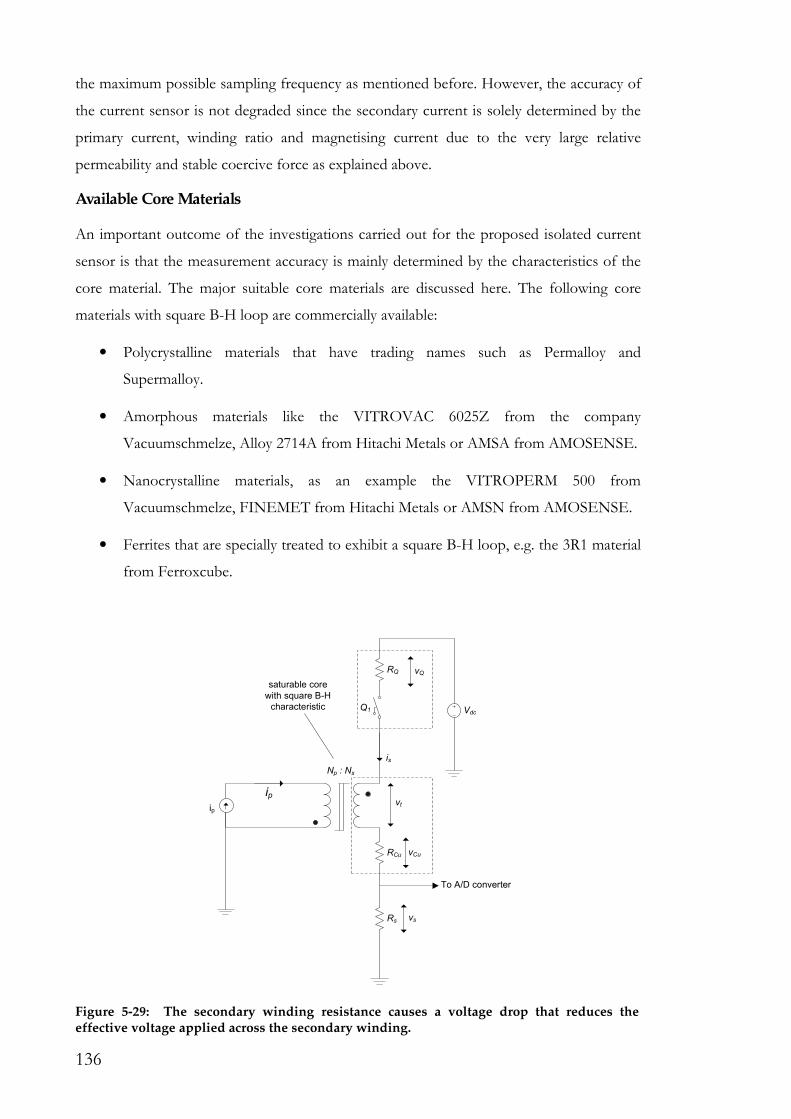
136
the maximum possible sampling frequency as mentioned before. However, the accuracy of
the current sensor is not degraded since the secondary current is solely determined by the
primary current, winding ratio and magnetising current due to the very large relative
permeability and stable coercive force as explained above.
Available Core Materials
An important outcome of the investigations carried out for the proposed isolated current
sensor is that the measurement accuracy is mainly determined by the characteristics of the
core material. The major suitable core materials are discussed here. The following core
materials with square B-H loop are commercially available:
• Polycrystalline materials that have trading names such as Permalloy and
Supermalloy.
• Amorphous materials like the VITROVAC 6025Z from the company
Vacuumschmelze, Alloy 2714A from Hitachi Metals or AMSA from AMOSENSE.
• Nanocrystalline materials, as an example the VITROPERM 500 from
Vacuumschmelze, FINEMET from Hitachi Metals or AMSN from AMOSENSE.
• Ferrites that are specially treated to exhibit a square B-H loop, e.g. the 3R1 material
from Ferroxcube.
RCu
Vdc
Np : Ns
vt
saturable core
with square B-H
characteristic
vs
Q1
ipip
is
Rs
To A/D converter
vCu
vQRQ
Figure 5-29: The secondary winding resistance causes a voltage drop that reduces the effective voltage applied across the secondary winding.

137
Polycrystalline materials are built with grain sizes between 50 µm and 100 µm and exhibit a
coercive force at DC of 5 to 0.3 A/m. The resistivity is smaller than that of the other
materials, which leads to increased eddy current losses. Although in general a decreasing
grain size leads to an increased coercive force, there is a change in this trend when the grain
size approaches the nanometre regime. The amorphous and nanocrystalline materials take
advantage of this behaviour and reach coercive forces below 1 A/m. At the same time, the
resistivity of these materials is larger compared to polycrystalline materials, which reduces
eddy current losses.
Nanocrystalline materials follow nearly the same production procedure as amorphous
materials but are to >80 % based on iron, whilst amorphous materials consist to >80 %
out of cobalt. Nanocrystalline materials support around twice the saturation flux density of
amorphous materials whilst providing very high relative permeability. This advantage
comes at the cost of a slightly lower resistivity and larger coercive force. However, the
market price for cobalt compared with iron is thirty times higher, which makes
nanocrystalline cores less expensive than amorphous cores.
There are also ferrite materials available that have been specially treated to exhibit a
rectangular B-H loop. However, such ferrites are in low demand, and the only ferrite
material available from a main producer of ferrites is the 3R1 material from Ferroxcube.
For this reason, the price for ferrite materials with square B-H loop is higher than for
standard ferrites but still notably lower than for any of the other materials.
The important material properties for the proposed current sensor are depicted in TABLE
-1.0
-0.5
0.0
0.5
1.0
0.0 0.5 1.0 1.5 2.0 2.5 3.0 3.5
i p [A]
Lin
eari
ty E
rro
r [%
]
Core 1 Core 2 Core 3
Figure 5-30: Measurement of the device-to-device stray characteristic due to the coercive force value.

138
5-VI. The saturation flux density is a key parameter in order to reduce the magnetic noise
immunity. Nanocrystalline materials clearly provide the highest saturation flux density, and
thus provide the best magnetic noise immunity. The coercive force is responsible for the
sensor’s offset voltage and should be as small as possible. Moreover, the hysteresis losses
are proportional to the coercive force. The company Hitachi Metals guarantees a tolerance
of ±15% for the coercive force value, which is sufficient to build current sensors with tight
initial tolerance without additional calibration during the production process. Figure 5-30
shows a measurement for three identical amorphous cores without calibration. The initial
tolerance is, obviously, very small and no initial calibration is required. It has been
mentioned before that the influence of the magnetising current on the absolute
measurement accuracy is inverse proportional to the maximum primary current, which
means that the initial tolerance is even less for current sensors that measure larger currents.
Nanocrystalline and amorphous materials have a very low apparent coercive force with low
temperature coefficient that enables the construction of current sensors with extremely low
thermal drift. The thermal drift of the amorphous 2714A alloy from Hitachi is shown in
Figure 5-31.
The squareness ratio (Br/Bsat) is a measure of the magnitude of the core’s relative
permeability in the linear region. TABLE 5-VI clearly shows that amorphous and
nanocrystalline materials have by far the highest squareness ratio, which yields a very large
relative permeability that minimises the linearity error and eliminates the dependence on
the supply voltage as discussed previously.
The Curie temperature determines the maximum possible operating temperature, which are
all above 200 °C. This demonstrates another advantage of the proposed current sensor
since the measurement principle works up to much higher temperatures than Hall Effect
devices that are usually limited to a value below 100°C. The maximum operating
temperature of the proposed sensor is generally restricted by switch Q1 that limits the
TABLE 5-VI: AVAILABLE MAGNETIC CORE MATERIALS
VITROVAC
6025 Z
(Amorphous)
VITROPERM
500 F
(Nanocrystalline)
Supermalloy
(Polycrystalline)
3R1
(Ferrite)
Bsat [T] 0.58 1.2 0.65 – 0.82 0.34 – 0.41
Hc @ DC [A/m] 0.3 ±15 % 0.9 – 1.1 0.32 – 1.2 23 – 52
TC(Hc) (ppm/K) 3,000 700 ? 10,000
Br/Bsat >0.96 >0.94 0.4 – 0.7 0.65 – 0.76
Tc [°C] 240 600 460 230
Rsc [µΩm] 1.35 1.2 0.57 1000

139
maximum ambient temperature to value around 150°C.
The material resistivity Rsc, finally, is a measure for the eddy current related power loss.
Ferrite materials clearly have the highest resistance, and thus the core losses in this material
are usually dominated by hysteresis and anomalous losses. However, the experimentally
derived apparent coercive force of the prototype sensor using amorphous material was 6.8
A/m, which is still several times smaller than the coercive force of a ferrite material at DC.
From the materials discussed above, amorphous and nanocrystalline materials clearly offer
the best measurement performance. Nanocrystalline materials provide larger saturation flux
density, which makes them more resistant against magnetic stray fields. Moreover, they are
less costly than amorphous materials. Since nanocrystalline and amorphous materials
consist of a wound ribbon, it can be difficult to produce certain core shapes like a flat
toroid. Ferrite, on the other hand, is the material with the lowest cost and can be produced
without difficulties in most shapes and sizes. Their biggest drawback is the distinct thermal
drift due to the large coercive force. Polycrystalline materials are generally more expensive
than amorphous materials and have inferior magnetic performance. Thus, they are not
suitable for the use in the proposed current sensor and are likely be replaced by amorphous
and nanocrystalline cores in several other applications.
The sensor performance using ferrite and amorphous material has been compared by
means of a prototype. The results depicted in TABLE 5-VII demonstrate that the
amorphous core achieves notably better performance at smaller core loss but is five times
more expensive.
5.6 Summary
The original circuit proposed by Severns enables the accurate measurement of direct
Figure 5-31: Change in the coercive force against temperature of the amorphous 2714A alloy from Hitachi metals.

140
currents at low cost. However, the inability to measure currents down to zero made it
impossible to employ this circuit in most current sensing applications. In this chapter, the
working principle has been analysed in detail and modifications have been proposed that
overcome this limitation. The most powerful embodiment forces a pulsed current through
an auxiliary winding in order to allow the measurement of currents down to zero. This
circuit exhibits significantly less power loss than the original Severns circuit by enabling the
recycling of the energy that is dissipated in the original Severns circuit inside the zenerdiode
during the off-time off the sampling switch. Based on this current sensing principle a low-
cost isolated voltage senor with good measurement accuracy has been derived that can
measure any positive current waveform. It is even possible to adapt this current sensor to
measure negative currents as found in 5.3.1.
Thorough hardware experiments have been carried out that revealed several practical
limitations like local saturation phenomena that occur if the primary current is not centred
inside the toroid core. Similar effects may occur if strong external magnetic stray fields
locally saturate the core material. It is further shown that core losses can be minimised by
choosing the right core material and that winding and switch resistance may reduce the
maximum sampling frequency but do not alter the measurement accuracy.
Finally, available core materials are discussed together with the influence on the current
sensing performance. It is shown that the offset voltage due to the magnetising current
does not need calibration during the production process since the manufactures of the
cores can control the magnetic parameter with sufficient precision. Hardware experiments
were carried out to compare the performance of Ferrite and amorphous core materials.
The sensor using the amorphous core material achieved clearly better measurement
performance but comes at five times the price.
TABLE 5-VII: COMPARISON OF THE SENSOR PERFORMANCE BETWEEN FERRITE AND AMORPHOUS
CORE MATERIAL
Ferrite (Ferroxcube 3R1) Amorphous ( Hitachi 2714A)
Size (OD/ID/HT) 9/6/3 9/6/3
Maximum Primary Current 15 A 15 A
Maximum Output Voltage 3 V 3 V
∆B 100 mT 100 mT
Sampling Frequency 100 kHz 100 kHz
Turns Ratio 1:100:50 1:100:50
Non-linearity < 0.2 % < 0.1 %
Offset Voltage @ ip = 0 127 mV 25 mV
Initial Tolerance < ±0.6% < ±0.1%
Thermal Drift < 650 ppm / K < 25 ppm / K
Core Loss 66.4 mW 13.6 mW
Cost @ 100k pieces USD 0.10 USD 0.50

141
In conclusion, a high-accuracy current sensor with large measurement bandwidth, very low
thermal drift and low cost has been developed. Several prototype sensors have been
successfully constructed with current ranges from 3 A up to 220 A. At currents below 3 A
the magnetising current relative to the primary current becomes significant and notably
increases thermal drift and non-linearity. On the other hand, above 220 A the primary
conductor should be carefully centred inside the toroid to avoid local saturation
phenomena.
The cost of the proposed current sensor is much lower than other electrical isolated DC
current sensors (refer to TABLE 2-II and TABLE 2-III) and is competitive with shunt
resistors. A shortcoming is that there is an induced voltage into the primary side, that is
given by the secondary transformer voltage times the turns ratio. This may pose a problem
in certain applications. However, in power converter applications the current sensor can be
connected in series to the input inductor of the PFC stage or the output inductor of the
DC-DC stage. The inductor will keep the current constant, and thus no noise is observable
at the input or output of the power converter.

142
Chapter 6
Conclusions
6.1 Problem Summary
As pointed out in Chapter 2 and Appendix I, recent advances in current sensing are not
driven by new physical current sensing principles but by more advanced material and
semiconductor technology. Thermal drift, non-linearity and hysteresis problems that made
some current sensing techniques unpractical in the past are nowadays mastered with the
help of highly integrated low-cost signal processors and better materials. In the same vein,
this thesis investigated known current sensing principles with problems that have not been
solved or thoroughly investigated until now:
• The copper trace current sense approach suffers from severe thermal drift and very
small output voltage.
• The output inductor current sense method also exhibits significant thermal drift
and in addition poor waveform fidelity.
• The Severns circuit provides a non-continuous output signal, is unable to measure
currents down to zero and needs additional control circuitry.
The problems of the above-mentioned current sensing methods have been solved by a
combination of advanced materials, circuit modifications and the use of digital signal
processing.
6.2 Copper Trace Current Sense Approach
Sensing the voltage drop across a shunt resistor is a proven and reliable technique that has
been extensively used over the last hundred years to measure current. However, in order to
143
use the copper trace as a replacement for the shunt resistor a temperature correction
becomes necessary to account for the large thermal drift of the copper resistance. This
thesis demonstrated that using a low-cost temperature sensor reasonable measurement
accuracy over a large operating range can be achieved. It has been demonstrated that the
dynamic performance is comparable with that of a shunt resistor if certain design
guidelines are followed. The copper trace current sense method is useful for measuring
large DC currents like the output current of a power converter as shown in Figure 1-4 at
position f) or g). This current information is needed in order to implement digital control,
overcurrent protection and monitoring functionalities. The copper trace current sense
approach is suitable to replace the commonly used shunt resistor in order to overcome the
power-loss, size and cost limitations of the shunt resistor.
6.3 Output Inductor Current Sensing with Coupled Sense Winding
The lossless output inductor current sensing approach has the advantage of higher output
voltage amplitude compared with the copper trace sense approach and is therefore often
employed in power conversion. Since measuring the voltage drop across the winding
resistance of an inductor is also based on Ohm’s law of resistance, it is considered a reliable
way to measure the current. This thesis proposes the coupled sense winding approach to
overcome the waveform fidelity limitation due to the variability of the inductance
parameters. The resulting dynamic performance is then competitive with the shunt resistor
and copper trace current sense approach. Moreover, the relatively large output voltage
relieves the design of the following amplification stage. This will allow the construction of
small, power-efficient and low-cost current sensing solutions, which are important to
enable the construction of high-efficient power supplies with superior power density.
However, this current sense method is limited to the case were the current of interest is
flowing through an inductor. In the discussed AC-DC converter topology, this current
sensing principle is especially suitable to measure the output current in Figure 1-4 at
position e). Moreover, due to the large output current the output inductor will have a small
number of turns, which makes the implementation of the coupled sense winding approach
less costly.
6.4 Modified Severns Circuit
A major problem of the two current sensors described above is that they are not electrically
isolated. Existing Hall Effect and AMR based electrical isolated current sensors do exhibit

144
electrical isolation but are too expensive for the use in AC-DC power converters. For this
reason, an inexpensive DC current sensor with electrical isolation was presented by Severns
at the applied power electronics conference and exposition (APEC) in 1986. This current
sensor is highly accurate but requires additional control circuitry, provides a non-
continuous output signal and is unable to measure currents down to zero. In this thesis, a
modified circuit is presented, which extends the measurement range to currents down to
zero and reduces the power loss of the original sensor by more than 50%. The switch
control signal that was a disadvantage in the past is now easy to implement in today’s
digitally controlled power converters. Moreover, the discontinuous output signal can be
directly sampled by an integrated analogue-to-digital converter.
Experiments with different core materials have been carried out to examine the
measurement performance of the proposed sensor. These experimental results indicate that
the linearity is not significantly influenced by the magnetic material as long as the relative
permeability is very large. A theoretical model of the current sensor has also been
developed that confirms this finding. The thermal drift using ferrite cores is much larger
than that of amorphous or nanocrystalline cores due to the much larger coercive force in
ferrite materials. By employing amorphous and nanocrystalline cores, very low thermal
drifts of 25 ppm/K for a 15 A prototype and 5 ppm/K for 220 A prototype have been
achieved. Nevertheless, the use of ferrite materials may still be justified in ultra low-cost
applications since the price of ferrites is up to five times smaller than that of amorphous or
nanocrystalline materials. It is further shown that the cross sectional area of the employed
core material determines the maximum achievable measurement bandwidth or sampling
frequency respectively. This is a desirable characteristic since reducing the cross sectional
area means reduced size and core losses. However, it has been found that a smaller core
cross sectional area is more susceptible to external magnetic fields, which can be explained
in terms of local saturation phenomena. Accordingly, there is a trade-off between core size
and magnetic noise immunity.
The modified Severns circuit is especially useful for measuring high frequency currents in
digital control applications that require a current sample at discrete time instants. One such
example is the primary current within an isolated full-bridge DC-DC converter (Position a)
in Figure 1-4) or the input current of a PFC stage (Position a) in Figure 1-3). Contemporary
solutions involve the use of a current transformer, which limits the maximum duty cycle
due to core saturation, and may reduce the conversion efficiency. In this configuration, a
trade off has to be made between maximum duty cycle and core cross sectional area. In
contrast, the modified Severns circuit can truly measure DC and does not limit the

145
maximum duty cycle. Moreover, the cross sectional area necessary for the magnetic core in
the Severns circuit can be made smaller than that of a comparable current transformer.
The proposed circuit is also able to measure currents beyond 100 A. A prototype for 220 A
has been built and employed to measure the output current of an AC-DC converter
(Position e) or f) in Figure 1-4). The measurement results yielded very good accuracy and
thermal drift characteristic. However, due to the large currents, local saturation of the
magnetic core has been observed that reduces the maximum allowed sampling rate. The
best performance can be achieved by having the toroid core carefully centred around the
conductor, so that the magnetic field inside the core is homogenous.
6.5 Future Research
6.5.1 Sensing Principles Based on Ohm’s Law of Resistance
The busbar current sense method described in Chapter 3 provides a very small output
voltage. An amplifier is necessary to make this output voltage large enough to sample via
an analogue-to-digital converter. While this thesis demonstrated the performance of the
naked busbar, a commercial successful current sensor needs a low-cost amplification stage
that does not notably deteriorate the accuracy of the busbar current sense method. The
construction and design of such an amplifier stage may need further investigation.
In Chapter 4 the coupled sense winding inductor current sense method has been presented,
which provides a larger output voltage than the busbar current sense method. Therefore,
the amplification is less complicated and not as critical. However, demonstrations that the
temperature sensing can be implemented cost efficiently and with sufficient accuracy are
required. As, in contrast to the busbar current sense method, the temperature sensor
cannot be fitted onto the output inductor easily, a larger temperature drop between the
copper and temperature sensor than that has been described for the busbar in Chapter 3
may occur.
6.5.2 Modified Severns Circuit
The modified Severns circuit discussed in Chapters 5 has a lot of potential for future
research.
Integrated Circuit Version
The circuit variants proposed so far aim to minimise the circuit complexity in order to
reduce components and production cost. However, it is possible to integrate the control

146
circuit into an IC to further reduce the number of components at the cost of a more
complex circuit. It is then possible to saturate the core material prior to the sampling
interval using the secondary winding instead of an additional auxiliary winding. This
required two switches, Qaux1 and Qaux2, to force the auxiliary current through the secondary
winding by commutating the current direction as illustrated in Figure 6-1. Once the core is
fully saturated, the sampling switches Qs1 and Qs2 are closed and force the core out of
saturation, and an analogue-to-digital converter then samples the voltage across Rs. If
required it is feasible to convert the current information back into an analogue value after
processing inside the control circuit by means of a digital-to-analogue converter. Once the
analogue-to-digital converter has sampled the sense voltage, switches Qs1 and Qs2 are
opened and force the current through the secondary winding to freewheel through diodes
D1, D2 and power supply Vdc. Similar to the circuit proposed in Figure 5-17, the power is
recycled and not dissipated except for the power loss inside the diodes.
As mentioned before, the auxiliary current needs only to be applied at currents close to
zero. Accordingly, the auxiliary current does not increase the maximum power loss of the
current sensor. Figure 6-1 shows the auxiliary current being generated by a current source,
since a current source is better suited for integration than a resistor.
This integrated circuit version has the same performance as the discrete embodiments
discussed before but does not need a separate auxiliary winding. This allows a reduction of
the size of the transformer, which also reduces the system cost. Moreover, the integrated
circuit will have much smaller size than the sum of all discrete components. The current
Figure 6-1: Integrated circuit version of the modified Severns circuit that uses only two windings.

147
range can simply be chosen by selecting the sense resistor Rs and the turns ratio for the
transformer. A drawback is the increased power losses since two switches in series are
needed for the auxiliary and sampling current and two diodes instead of one to conduct the
freewheeling current.
Rogowski Coil Mode
Another potential modification is to combine the proposed modified Severns circuit with
the Rogowski coil principle that has been described in Chapter 2. The Rogowski coil is
wound around a non-magnetic toroid core that surrounds the conductor carrying the
current that needs to be measured. Advantages of the Rogowski coil are low current
consumption and high bandwidth, but without ability to measure DC currents. The current
sensor described in Chapter 5, on the other hand, uses a magnetic core with large relative
permeability. However, if the core material is saturated the relative permeability decreases
to one and the core behaves exactly like a non-magnetic material. So it is possible that the
proposed current sensor can also be operated in a Rogowski coil mode by integrating the
voltage across the secondary winding during the saturated state as illustrated in Figure 6-2.
Combining the proposed sensor with the Rogowski coil operation opens a new field of
interesting opportunities. The central idea is to sample the current with the proposed
Rs
Vdc
Digital Processor
Np : Ns
Na
vt
saturable core
with square B-H
characteristic
vs
Q2
ia
Q1
A/D
with S/H
ip
is
R1
D1
∫
Figure 6-2: Combination of the modified Severns circuit with a Rogowski coil.

148
method while the integrator is activated once the core is back in saturation, allowing it to
track the current even if switch Q1 is open. By periodically taking a current sample by
closing switch Q1, the offset drift of the integrator can be compensated yielding a current
sensor with very high bandwidth and DC capability. This method has the potential to
significantly boost the bandwidth of the proposed current sensor up to a corner frequency
given by the Rogowski coil.

149
Bibliography
[1] R. Malik, "Digital power management and power control, and its impact on the
industry," presented at Darnell's Digital Power Forum, San Francisco, CA, 2007.
[2] ---, "Climate Savers Computing Initiative White Paper," Climate Savers [Online].
Available: www.climatesaverscomputing.org, 2008.
[3] Y. Jang, M. M. Jovanovic, and D. L. Dillman, "Hold-up time extension circuit with
integrated magnetics," IEEE Trans. Power Electronics, vol. 21, pp. 394-400, 2006.
[4] R. W. Erickson and D. Maksimovic, Fundamentals of power electronics. New York:
Springer Science+Business Media, Inc., 2001.
[5] S. Ziegler, R. C. Woodward, H. H. C. Iu, and L. J. Borle, "Current sensing
techniques: A review," IEEE Sensors Journal, vol. 9, pp. 354-376, 2008.
[6] A. V. Peterchev and S. R. Sanders, "Digital multimode buck converter control with
loss-minimizing synchronous rectifier adaptation," IEEE Trans. Power Electronics, vol. 21,
pp. 1588-1599, 2006.
[7] J. A. Abu-Qahouq, H. Mao, H. J. Al-Atrash, and I. Batarseh, "Maximum efficiency
point tracking (MEPT) method and dead time control," in Power Electronics Specialists
Conference, PESC, vol. 5, 2004, pp. 3700- 3706.
[8] R. Mammano, "Switching power supply topology - Voltage mode vs. current
mode," Unitrode Design Note DN-62, 1999.
[9] H. Mao, L. Yao, S. Deng, O. Abdel-Rahman, J. Liu, and I. Batarseh, "Inductor
current sharing of current doubler rectifier in isolated DC-DC converters," in Applied Power
Electronics Conference and Exposition, APEC. Dallas, TX, 2006, pp. 770-775.
150
[10] B. Yang, P. Xu, and F. C. Lee, "Range winding for wide input range front end
DC/DC converter," in Applied Power Electronics Conference and Exposition, APEC, vol. 1, 2001,
pp. 476 - 479
[11] Y.-F. Liu and P. K. Jain, "A new current sensing scheme for zero-voltage switching
phase-shifted bridge converter," presented at Twenty-second International
Telecommunications Energy Conference, INTELEC, Phoenix, AZ, 2000.
[12] B. Mammano, "Paralleling power: Choosing and applying the best technique for
load sharing," in Power Design Seminar SEM 1500, Unitrode Corp., 2002.
[13] E. Dallago, M. Passoni, and G. Sassone, "Lossless current sensing in low-voltage
high-current DC/DC modular supplies," IEEE Trans. Industrial Electronics, vol. 47, pp.
1249-1252, 2000.
[14] F. W. Grover, Inductance calculations: Working formulas and tables. New York: D. Van
Nostrand, 1946.
[15] C. M. Johnson and P. R. Palmer, "Current measurement using compensated coaxial
shunts," IEE Proceedings - Science, Measurement and Technology, vol. 141, pp. 471-480, 1994.
[16] J. A. Ferreira, W. A. Cronje, and W. A. Relihan, "Integration of high frequency
current shunts in power electronic circuits," IEEE Trans. Power Electronics, vol. 10, pp. 32-
37, 1995.
[17] R. Malewski, "New device for current measurement in exploding wire circuits,"
Review of Scientific Instruments, vol. 39, pp. 90-94, 1968.
[18] R. Malewski, C. T. Nguyen, K. Feser, and N. Hylten-Cavallius, "Elimination of the
skin effect error in heavy-current shunts," IEEE Trans. Power Apparatus and Systems, vol.
PAS-100, pp. 1333-1340, 1981.
[19] F. Castelli, "The flat strap sandwich shunt," IEEE Trans. Instrumentation and
Measurement, vol. 48, pp. 894-898, 1999.
[20] F. Costa, P. Poulichet, F. Mazaleyrat, and E. Labouré, "The current sensors in
power electronics, a review " EPE Journal, vol. 11, pp. 7-18, 2001.
[21] B. Mammano, "Current sensing solutions for power supply designer," in Power
Design Seminar SEM 1200, Unitrode Corp., 1997.
[22] ---, "High-side current-sense measurement," Appl. Rep. AN 746, Maxim Integrated
Products Inc., 2005.

151
[23] L. Spaziani, "Using copper PCB etch for low value resistance," Appl. Rep. DN-71,
Texas Instruments, 1997.
[24] G. Eirea and S. R. Sanders, "High precision load current sensing using on-line
calibration of trace resistance," IEEE Trans. Power Electronics, vol. 23, pp. 907-914, 2008.
[25] Y. Zhang, R. Zane, A. Prodic, R. Erickson, and D. Maksimovic, "Online calibration
of MOSFET on-state resistance for precise current sensing," IEEE Power Electronics Letters,
vol. 2, pp. 100 - 103, 2004.
[26] D. Grant and R. Pearce, "Dynamic performance of current-sensing power
MOSFETs," IEEE Electronics Letters, vol. 24, pp. 1129-1131, 1988.
[27] C. F. Lee and P. K. T. Mok, "A monolithic current-mode CMOS DC–DC
converter with on-chip current-sensing technique," IEEE Journal of Solid State Circuits, vol.
39, pp. 3-14, 2004.
[28] X. Zhou, P. Xu, and F. C. Lee, "A novel current-sharing control technique for low-
voltage high-current voltage regulator module applications," IEEE Trans. Power Electronics,
vol. 15, pp. 1153-1162, 2000.
[29] H. P. Forghani-zadeh and G. A. Rincón-Mora, "An accurate, continuous, and
lossless self-learning CMOS current-sensing scheme for inductor-based DC-DC
converters," IEEE Journal of Solid State Circuits, vol. 42, pp. 665-679, 2007.
[30] W. F. Ray and C. R. Hewson, "High performance Rogowski current transducers,"
in IEEE Industry Applications Conferences. Rome, Italy, 2000, pp. 3083–3090.
[31] ---, "RCTrms Rogowski coil datasheet," Power Electronic Measurements Ltd.
[Online]. Available: http://www.pemuk.com, 2005.
[32] D. A. Ward and J. L. T. Exon, "Using Rogowski coils for transient current
measurements," Engineering Science and Education Journal, vol. 2, pp. 105-113, 1993.
[33] A. Radun, "An alternative low-cost current-sensing scheme for high-current power
electronics circuits," IEEE Trans. Industrial Electronics, vol. 42, pp. 78-84, 1995.
[34] L. Dalessandro, N. Karrer, M. Ciappaz, A. Castellazzi, and W. Fichtner, "Online
and offline isolated current monitoring of parallel switched high-voltage multi-chip IGBT
modules," in 39th IEEE Power Electronics Specialists Conference, PESC'08. Rhodes, Greece,
2008, pp. 2600-2606.
152
[35] L. Zhao, J. D. v. Wyk, and W. G. Odendaal, "Planar embedded pick-up coil sensor
for integrated power electronic modules," in Applied Power Electronics Conference and
Exposition, APEC, vol. 2. Anaheim, California, 2004, pp. 945-951.
[36] J. P. Dupraz, A. Fanget, W. Grieshaber, and G. F. Montillet, "Rogowski coil:
Exceptional current measurement tool for almost any application," in IEEE Power
Engineering Society General Meeting. Tampa FL, USA, 2007, pp. 1-8.
[37] N. McNeill, N. K. Gupta, S. G. Burrow, D. Holliday, and P. H. Mellor,
"Application of reset voltage feedback for droop minimization in the unidirectional current
pulse transformer," IEEE Trans. Power Electronics, vol. 23, pp. 591-599, 2008.
[38] N. McNeill, N. K. Gupta, and W. G. Armstrong, "Active current transformer
circuits for low distortion sensing in switched mode power converters," IEEE Trans. Power
Electronics, vol. 19, pp. 908-917, 2004.
[39] K.-w. Ma and Y.-s. Lee, "Technique for sensing inductor and DC output currents
of PWM DC-DC converter," IEEE Trans. Power Electronics, vol. 9, pp. 346-354, 1994.
[40] ---, "Isolated current and voltage transducers," Appl. Rep., LEM, 2004.
[41] L. Dalessandro, N. Karrer, and J. W. Kolar, "High-performance planar isolated
current sensor for power electronics applications," IEEE Trans. Power Electronics, vol. 22,
pp. 1682-1691, 2007.
[42] P. Poulichet, F. Costa, and É. Labouré, "A new high-current large-bandwidth dc
active current probe for power electronics measurements," IEEE Trans. Industrial Electronics,
vol. 52, pp. 243-254, 2005.
[43] P. A. Tipler, Physics for scientists and engineers. New York, USA: Worth Publishers Inc,
1991.
[44] ---, "An introduction to the Hall Effect," Bell Technologies Inc. [Online]. Available:
http://www.fwbell.com, 2005.
[45] ---, "Understanding Hall Effect Devices," Bell Technologies Inc. [Online].
Available: http://www.fwbell.com, 2005.
[46] R. S. Popovic, Z. Randjelovic, and D. Manic, "Integrated Hall-effect magnetic
sensors," Sensors and Actuators A: Physical, vol. 91, pp. Pages 46-50, 2001.
[47] J. Lenz and A. S. Edelstein, "Magnetic sensors and their applications," IEEE Sensors
Journal, vol. 6, pp. 631-649, 2006.

153
[48] P. Ripka, "Review of fluxgate sensors," Sensors and Actuators A: Physical, vol. 33, pp.
129-141, 1992.
[49] F. Primdahl, "The fluxgate magnetometer," Journal of Physics E: Scientific Instruments,
vol. 12, pp. 241-253, 1979.
[50] P. Ripka, "Advances in fluxgate sensors," Sensors and Actuators A: Physical, vol. 106,
pp. 8-14, 2003.
[51] F. Primdahl, "The fluxgate mechanism, part I: The gating curves of parallel and
orthogonal fluxgates," IEEE Trans. Magnetics, vol. 6, pp. 376-383, 1970.
[52] S. Ziegler, P. Gammenthaler, and A. Chapuis, "An isolated current to voltage,
voltage to voltage converter," U. S. P. T. Office, Ed. USA: Power-One Inc., 2008
(Application filed).
[53] S. Ziegler, L. Borle, and H. H. C. Iu, "Transformer based DC current sensor for
digitally controlled power supplies," in Australasian Universities Power Engineering Conference
2007. Perth, Australia, 2007, pp. 525-530.
[54] M. Román, G. Velasco, A. Conesa, and F. Jeréz, "Low consumption fluxgate
transducer for AC and DC high-current measurement," in 39th IEEE Power Electronics
Specialists Conference, PESC'08. Rhodes, Greece, 2008, pp. 535-560.
[55] P. Pejovic, "A simple circuit for direct current measurement using a transformer,"
IEEE Trans. Circuits and Systems-I: Fundamental Theory and Applications, vol. 45, pp. 830-837,
1998.
[56] I. M. Filanovsky and V. A. Piskarev, "Sensing and measurement of DC current
using a transformer and RL-multivibrator," IEEE Trans. Circuits and Systems, vol. 38, pp.
1366-1370, 1991.
[57] K. Harda and H. Sakamoto, "Current sensors with a small saturable core and
MOSFETs," IEEE Trans. Magnetics, vol. 24, pp. 2910-2912, 1988.
[58] Pavel Ripka, Jan Kubik, Maeve Duffy, William Gerard Hurley, and S. O’Reilly,
"Current sensor in PCB technology," IEEE Sensors Journal, vol. 5, pp. 433-438, 2005.
[59] O. Dezuari, E. Belloy, S. E. Gilbert, and M. A. M. Gijs, "Printed circuit board
integrated fluxgate sensor," Sensors and Actuators A: Physical, vol. 81, pp. 200-203, 2000.
[60] ---, "Basic introduction to the use of magnetoresistive sensors," Appl. Rep. AN 37,
Zetex Semiconductors Inc., 2003.

154
[61] G. Laimer and J. W. Kolar, "Design and experimental analysis of a DC to 1 MHz
closed loop magnetoresistive current sensor," in Applied Power Electronics Conference and
Exposition, APEC'05, vol. 2. Austin, Texas, 2005, pp. 1288-1292.
[62] G. Binasch, P. Grünberg, F. Saurenbach, and W. Zinn, "Enhanced
magnetoresistance in layered magnetic structures with antiferromagnetic interlayer
exchange," Physical Review B, vol. 39, pp. 4828-4830, 1989.
[63] M. N. Baibich, J. M. Broto, A. Fert, F. N. V. Dau, F. Petroff, P. Eitenne, G.
Creuzet, A. Friederich, and J. Chazelas, "Giant magnetoresistance of (001)Fe/(001)Cr
magnetic superlattices," Physical Review Letters, vol. 61, pp. 2472-2475, 1988.
[64] ---, "The giant magnetoresistive head: A giant leap for IBM research," IBM
Research [Online]. Available: http://www.research.ibm.com/research/gmr.html, 1997.
[65] K.-M. H. Lenssen, D. J. Adelerhof, H. J. Gassen, A. E. T. Kuiper, G. H. J. Somers,
and J. B. A. D. v. Zon, "Robust giant magnetoresistance sensors," Sensors and Actuators A:
Physical, vol. 85, pp. 1-8, 2000.
[66] C. Reig, D. Ramirez, F. Silva, J. Bernardo, and P. Freitas, "Design, fabrication, and
analysis of a spin-valve based current sensor," Sensors and Actuators A: Physical, vol. 115, pp.
259-266, 2004.
[67] H. Beltran, C. Reig, V. Fuster, D. Ramírez, and M. D. Cubells-Beltrán, "Modeling
of magnetoresistive-based electrical current sensors: A technological approach," IEEE
Sensors Journal, vol. 7, pp. 1532-1537, 2007.
[68] ---, "AA and AB-series analog sensors datasheet," NVE Inc. [Online]. Available:
http://www.nve.com, 2005.
[69] I. Jedlicska, R. Weiss, and R. Weigel, "Improving GMR current sensor
measurements through hysteresis modeling," in 39th IEEE Power Electronics Specialists
Conference, PESC'08. Rhodes, Greece, 2008, pp. 4781-4785.
[70] P. Kowina, H. Reeg, A.Peters, M. Haepe, W.-J. Becker, and W. Ricken, "High
dynamic magnetic beam current measurement by means of optimized magnet-resistance
(MR) sensor engineering," in 7th European Workshop on Beam Diagnostics and Instrumentation for
Particle Accelerators, DIPAC 2005. Lyon, 2005, pp. 102-104.
[71] X. P. Li, Z. J. Zhao, C. Chua, H. L. Seet, and L. Lu, "Enhancement of giant
magnetoimpedance effect of electroplated NiFe/Cu composite wires by dc Joule
annealing," J. Appl. Phys., vol. 94, pp. 7626–7630, 2003.

155
[72] R. S. Beach and A. E. Berkowitz, "Giant magnetic field dependent impedance of
amorphous FeCoSiB wire," Appl. Phys. Lett., vol. 64, pp. 3652–3654, 1994.
[73] T. Miyazaki and N. Tezuka, "Giant magnetic tunneling effect in Fe/Al2O3/Fe
junction," J. Magnetism and Magnetic Materials, vol. 139, pp. 231-234, 1994.
[74] D. D. Djayaprawira, K. Tsunekawa, M. Nagai, H. Maehara, S. Yamagata, N.
Watanabe, S. Yuasa, Y. Suzuki, and K. Ando, "230% room-temperature magnetoresistance
in CoFeB/MgO/CoFeB magnetic tunnel junctions," Appl. Phys. Lett., vol. 86, pp. 092502,
2005.
[75] E. Udd, Fiber optic sensors - An introduction for engineers and scientists. New York: John
Wiley & Sons, Inc., 1991.
[76] B. Lee, "Review of the present status of optical fiber sensors," Optical Fiber
Technology, vol. 9, pp. 57–79, 2003.
[77] K. Bohnert, P. Gabus, J. Nehring, H. Brändle, and M. G. Brunzel, "Fiber-optic
current sensor for electrowinning of metals," J. Lightwave Technol., vol. 25, pp. 1-8, 2007.
[78] K. Bohnert, H. Brändle, M. G. Brunzel, P. Gabus, and P. Guggenbach, "Highly
accurate fiber-optic DC current sensor for the electrowinning Industry," IEEE Trans.
Industry Applications, vol. 43, pp. 180-187, 2007.
[79] A. Papp and H. Harms, "Magnetooptical current transformer 1: Principles," Appl.
Opt., vol. 19, pp. 3729–3734, 1980.
[80] T. W. Cease and P. Johnston, "A magneto-optic current transducer," IEEE Trans.
Power Delivery, vol. 5, pp. 548-555, 1990.
[81] P. A. Nicati and P. Robert, "Stabilized current sensor using a Sagnac
interferometer," J. Phys. E: Sci. Instrum., vol. 21, pp. 791–796, 1988.
[82] A. J. Rogers, J. Xu, and J. Yao, "Vibration immunity for optical-fiber current
measurement," J. Lightwave Technol., vol. 13, pp. 1371-1377, 1995.
[83] M. J. Blake, P. Tantaswadi, and R. T. d. Carvalho, "In-line Sagnac interferometer
current sensor," IEEE Trans. Power Delivery, vol. 11, pp. 116-121, 1996.
[84] K. Bohnert, P. Gabus, J. Nehring, and H. Brändle, "Temperature and vibration
insensitive fiber-optic current sensor," Journal of Lightwave Technology, vol. 20, pp. 267-276,
2002.
[85] A. H. Rose, S. M. Etzel, and C. M.Wang, "Verdet constant dispersion in annealed
optical fiber current sensors," J. Lightwave Technol., vol. 15, pp. 803–807, 1997.

156
[86] S. X. Short, P. Tantaswadi, R. T. de Carvalho, B. D. Russell, and J. Blake, "An
experimental study of acoustic vibration effects in optical fiber current sensors," IEEE
Trans. Power Delivery, vol. 11, pp. 1702-1706, 1996.
[87] G. Frosio and R. Dändliker, "Reciprocal reflection interferometer for a fiber-optic
Faraday current sensor," Appl. Opt., vol. 33, pp. 6111-6122, 1994.
[88] R. Severns, "Improving and simplifying high frequency DC current sensors," in
Applied Power Electronics Conference and Exposition, APEC, 1986, pp. 180-182.
[89] D. E. Destefan and R. S. Stant, "AC and DC shunts - Can you believe their specs?,"
in 20th IEEE Instrumentation and Measurement Technology Conference, IMTC '03, vol. 2. Vail,
Colorado, USA, 2003, pp. 1577-1582.
[90] ---, "Cu-ETP copper specification," German Copper Institute [Online]. Available:
http://www.kupfer-institut.de/front_frame/pdf/Cu-ETP.pdf, 2005.
[91] D. W. Braudaway, "Behavior of resistors and shunts: With today’s high-precision
measurement capability and a century of materials experience, what can go wrong?," IEEE
Trans. Instrumentation and Measurement, vol. 48, pp. 889-893, 1999.
[92] B. Carter and T. R. Brown, "Handbook of operational amplifiers applications,"
Appl. Rep. SBOA092A, Texas Instruments, 2001.
[93] E. Weber, Electromagnetic Theory. New York: Dover, 1965.
[94] D. J. Griffiths, Introduction to Electrodynamics, 2 ed. New Jersey: Prentice-Hall Inc.,
1989.
[95] M. Kamon, M. Tsuk, and J. White, "FASTHENRY: A multipole accelerated 3-D
inductance extraction program," IEEE Trans. Microwave Theory and Techniques, vol. 42, pp.
1750–1758, 1994.
[96] C. Chang, "Lossless current sensing and its application in current mode control," in
39th IEEE Power Electronics Specialists Conference, PESC'08. Rhodes, Greece, 2008, pp. 4086-
4091.
[97] G. Garcea, S. Saggini, D. Zambotti, and M. Ghioni, "Digital autotuning system for
inductor current sensing in voltage regulation module applications," IEEE Trans. Power
Electronics, vol. 23, pp. 2500-2506, 2008.
[98] Z. Lukić, Z. Zhao, S. M. Ahsanuzzaman, and A. Prodić, "Self-tuning digital current
estimator for low-power switching converters," in 23rd IEEE Applied Power Electronics
Conference and Exposition, APEC'08, 2008, pp. 529-534.

157
[99] S. Ziegler, R. C. Woodward, H. H. C. Iu, and L. J. Borle, "Investigation into static
and dynamic performance of the copper trace current sense method," IEEE Sensors Journal,
vol. 9, pp. 782-792, 2009.
[100] F. Ohms, "Circuit arrangement for detecting a current in power supply devices," U.
S. P. T. Office, Ed. USA: ANT Nachrichtentechnik GmbH, 1987.
[101] A. V. Gillow and W. P. Marple, "Current sensor for low pass filter," U. S. P. T.
Office, Ed. USA: IBM Corporation, 1973.
[102] B. L. Wilkinson, "Power supply current detector system," U. S. P. T. Office, Ed.
USA: Pioneer Magnetics Inc., 1973.
[103] J. A. Houldsworth, "Purpose-designed ferrite toroids for isolated current
measurement in power electronic equipment," Electronics Components and Applications, vol. 3,
pp. 101-109, 1981.
[104] G. E. Schwarze, "Magnetic and electrical characteristics of permalloy thin tape
bobbin cores," presented at Second International Energy Conversion Engineering
Conference, Rhode Island, 2004.
[105] W. Shen, F. F. Wang, D. Boroyevich, and C. W. Tipton, "Loss characterization and
calculation of nanocrystalline cores for high-frequency magnetics applications," IEEE
Trans. Power Electronics, vol. 23, pp. 475-484, 2008.
[106] R. Street and D. C. Crew, "Fluctuation Aftereffect in Magnetic Materials," IEEE
Trans. Magnetics, vol. 35, pp. 4407-4413, 1999.
[107] M. P. Sharrock, "Measurement and interpretation of magnetic time effects in
recording media," IEEE Trans. Magnetics, vol. 35, pp. 4414-4422, 1999.
[108] M. El-Hilo, A. M. d. Witte, K. O'Grady, and R. W. Chantrell, "The sweep rate
dependence of coercivity in recording media," Journal of Magnetism and Magnetic Materials, vol.
117, pp. 307-310, 1992.
[109] J. Li, T. Abdallah, and C. R. Sullivan, "Improved calculation of core loss with
nonsinusoidal waveforms," in Conference Record of the 2001 IEEE Industry Applications
Conference, vol. 4, 2001, pp. 2203-2210.
[110] M. A. Willard, T. Francavilla, and V. G. Harris, "Core-loss analysis of an (Fe, Co,
Ni)-based nanocrystalline soft magnetic alloy," Journal of Applied Physics, vol. 97, pp. 1-3,
2005.

158
[111] L. A. Geddes, "Looking back - How measuring electric current has improved
through the ages," IEEE Potentials, vol. 15, pp. 40-43, 1996.
[112] E. Favre and W. Teppan, "Current sensing in electric drives - A future and history
based on multiple innovations," presented at 6th Symposium on Advanced
Electromechanical Motion Systems, Lausanne, Switzerland, 2005.
[113] E. Weston, "Shunt for electric light and power stations," U. S. P. T. Office, Ed.
USA, 1893.
[114] M. Macedonia, "It’s the end of the tube as we know It," in Computer, vol. 39, 2006,
pp. 83-85.
[115] Panther, "Diagram of D'Arsonval / Weston type galvanometer," Wikimedia
Commons, 2006.
[116] W. Rogowski and W. Steinhaus, "Die Messung der magnetischen Spannung,"
Archiv für Elektrotechnik, vol. 1, pp. 141-150, 1912.
[117] H. F. Storm, Magnetic amplifiers. New York: Wiley and Sons, 1955.
[118] W. Thomson, "On the Electro-Dynamic Qualities of Metals: Effects of
Magnetization on the Electric Conductivity of Nickel and of Iron," Proceedings of the Royal
Society of London, vol. 8, pp. 546-550, 1856.

159
Appendices
Appendix I
The History of Current Sensing
The Beginnings
Soon after Oersted discovered in 1820 that a current deflects a compass needle, Schweigger
developed the first current sensor, the so-called tangent galvanometer (Figure A-1) [111].
The tangent galvanometer forces the current to be measured to flow around a compass
needle, so that the resulting magnetic field deflects the needle from pointing northwards.
However, before the current was switched on, the instrument needed to be aligned to the
Earth’s magnetic field. A more sophisticated version called astatic galvanometer, which
eliminated the alignment procedure with the Earth’s magnetic field, has been invented by
Nobili (1825). It included a second compass needle attached parallel underneath the first
but with opposite magnetic polarisation [111]. Only one of the two needles is then placed
inside the coil that carries the current. Accordingly, this current sensor does not rely on the
Earth’s magnetic field anymore. The magnetic field due to the current flowing through the
coil generates a torque in the compass needle that is counteracted by a suspension. Since
the magnetic field of the current to be measured is multiplied by the number of turns of
the coil, these current sensors were also known as multipliers.
However, these early galvanometers were still highly susceptible against external magnetic
stray fields. In 1882 two French scientists, Jaques-Arsène d’Arsonval and Marcel Deprez,
proposed the use of a stationary permanent magnet and a coil with multiple turns, so that
external fields become negligible small compared to the magnetic field generated by the
permanent magnet (Figure A-2). The current to be measured flows through the coil and
experiences a torque due to the Lorentz force. Since a linear spring counteracts this torque,

160
the declination of the attached needle is a linear measure of the flowing current. The first
commercial product based on this design was brought onto the market by Edward Weston
in 1888 [111]. For the first time, a current sensor insensitive to the mounting position and
with linear characteristic was available.
To this point, the current to be measured flowed through the measurement instrument,
and thus the power loss due to the copper resistance of the coil inside the galvanometer
limited the maximum current. For large currents, this method became increasingly
impractical, and Edward Weston added a parallel shunt resistor to the galvanometer. The
shunt resistor bypassed the majority of the current, which allowed it to measure large
currents with a small coil and a reduced power loss. He patented this idea in 1893 [113].
Invented in 1897 by Karl Ferdinand Braun, the cathode ray tube (CRT) oscilloscope
enabled the measurement of fast changing signals [114]. It was now possible to measure the
current waveform, and thus the need for high-frequency shunt resistors became evident.
As a result, scientists started to develop shunt resistors with improved transient
performance. Silsbee found in 1916 that a coaxial structure provides extraordinary
measurement bandwidth. In the coaxial structure, the flowing current does not generate a
magnetic field in the centre of the shunt. This phenomenon can be exploited by connecting
the sense wires at the inside walls of the coaxial shunt. Since no magnetic field couples into
the sense wires, no voltage is induced and the measurement bandwidth is large. The
remaining problem was the skin effect, which changes the apparent resistance during
transient conditions. In the sixties and seventies researchers were working intensively on a
solutions for this problem, which was found by arranging the sense wires inside the wall of
the coaxial shunt. Inside the wall of the coaxial shunt the magnetic field is non-zero and
therefore a voltage is induced into the sense wires. By carefully adjusting the magnetic field
enclosed by the sense wires, the induced negative voltage can perfectly compensate the
increase in apparent resistance due to skin effect. This method can be explained by
Figure A-1: The tangent galvanometer invented 1821 was one of the first current sensors [112].

161
transient skin effect theory [17, 18].
With the help of a current transformer, which consist out of a transformer with high turns
ratio that is loaded at the secondary side with a sense resistor, the Weston galvanometer
was also able to measure large alternating currents. The current transformer, invented in
the 19th century, allowed it to step-down the current to reduce the power loss in the shunt
resistor. At the same time, the current transformer provides electrical isolation.
Yet another technique to measure alternating currents that provides electrical isolation and
low power loss is the Rogowski coil. The Rogowski coil is a core-less unloaded current
transformer alternative originally described by Rogowski and Steinhaus in 1912 [116].
However, the output voltage of this coil needs to be integrated by means of additional
circuitry before a galvanometer can be used to measure the output voltage.
It is interesting to note that even before the first Hall Effect current sensor was introduced,
current sensing techniques able to measure direct currents by providing electrical isolation
existed. An early direct current sensor mentioned for the first time in literature during the
thirties is depicted in Figure A-3 [53, 88, 112, 117]. The underlying physical principle is
related to fluxgates that were invented during the same period. In particular, this direct
current sensor exploits the saturation phenomenon of two identical transformers having
different polarised secondary windings. The current to be measured, ip, is sufficiently large
to hold both transformer cores in saturation. However, the applied AC supply voltage,
having square wave or sinusoidal waveform, forces one of the two transformers out of
saturation depending on the polarity of vAC. During this time, the transformer is in its linear
mode and produces a secondary current proportional to the turn ratio. This current is
rectified and can be measured as a voltage drop across the sense resistor Rs. Although
Figure A-2: Galvanometer invented by Jaques-Arsène d’Arsonval, Marcel Deprez and
Edward Weston that exhibits good magnetic noise immunity and is insensitive to the
mounting position [115].

162
problems arise because of the necessary large number of secondary turns N to reduce
resistive power losses in Rs, this DC current sensor achieves high precision and is able to
measure large currents on high voltage potentials due to the electrical isolation.
Progress Made Within the Last Fifty Years
In contrast to the beginnings, the progress in current sensing technology over the last fifty
years is mainly based on advances in semiconductor technology. A good example is the
Hall Effect: Although the Hall Effect was discovered 1879 by Edwin Hall, it was not until
the fifties that semiconductor materials with large Hall constants became available, so that
the resulting output voltage was sufficiently large for current sensing applications. Because
the Hall Effect voltage exhibits distinct thermal drift and offset, a more complex closed-
loop design has been introduced a few years later. This closed-loop design does not directly
rely on the stability of the Hall Effect voltage, and thus provides a far superior
measurement accuracy (< ±1%) [112].
Semiconductors also enabled the integration of complicated circuits into a small package
(IC). Thus, complex analogue and digital circuits can now be realised at small cost and size.
Consequently, the current information is no longer visualised with galvanometers but
digitalised using integrated analogue-to-digital converters for further processing, and
eventually visualized by a display device. Inexpensive microcontrollers and signal
processors can nowadays process the digitalised current information using sophisticated
digital compensation techniques to improve the performance of existing current sensors.
They can easily implement temperature, offset, hysteresis and linearity compensation
techniques without significant increase in cost or size. As an example, it is now possible to
build less expensive open-loop Hall Effect current sensors with ±1.5% accuracy by
combining them with integrated circuits to compensate for thermal drift, non-linearity and
offset [40].
Rs
N:1
N:1
ip
is
vs
T1
T2
vAC
ip
saturable cores with
square B-H
characteristic
+
-
~
~
+
-
Figure A-3: A direct current sensor that was in use before Hall Effect current transducers
became available.

163
Recent developments in shunt resistor and current transformer technology concentrate
mainly on making the current sensor smaller and less expensive. Nowadays, shunt resistors
are available as surface-mounted-devices (SMD) and use a combination of materials with
overall low temperature coefficient. However, coaxial shunt resistors still provide the best
transient performance because of the superior geometry [5]. Current transformers, on the
other hand, have benefitted from advanced core materials (Ferrite, Fe/Co-based
amorphous, Fe-based nanocrystalline), which exhibit less core loss, higher saturation level
and lower cost.
Within the last few decades, inexpensive magnetic field sensors other than Hall Effect or
Fluxgates became available that can be employed to sense currents. One example is the
magneto-resistance (AMR) effect, which has been discovered by William Thomson in 1856
[118]. He found that some materials change their resistance if they are exposed to a
magnetic field. Engineers are now building current sensors based on the magneto-
resistance effect. As an example, current sensors exploiting the anisotropic magneto-
resistance are commercially available for a few years while current sensors using the giant
magneto-resistance (GMR) are currently under investigation in a number of research
laboratories [5]. This development became possible due to the availability of inexpensive
digital compensation techniques, better materials, and improved manufacturing capabilities.
This is particularly true for sensors based on the GMR effect, which relies on digital
compensation techniques to rectify its distinct hysteresis behaviour.
Lately, some researchers have started to pursue a completely different approach to sense
currents. Their current sensing technique makes use of the Faraday Effect or Faraday
rotation discovered by Michael Faraday in 1845, who observed that magnetic fields linearly
rotate the polarisation of light. At present, a small number of companies have successfully
released commercial optical current sensor to measure very large alternating and direct
currents by providing outstanding electrical isolation. These sensors are able to measure
currents up to 500 kA [77]. Key technologies that were required in order to develop this
technique: Fibre-optic cables that do not exhibit bending stress, integrated optical phase
modulators together with semiconductor lasers and photodiodes. Moreover, a signal
processor is necessary to process the output signal and control the phase modulator.
Summary
Current sensing technologies attract the interest of scholars since the discovery of
electricity. The fundamental physical principles have been found during the 19th century

164
with Ohm’s law of resistance (1827), Faraday’s law of induction (1831), Faraday Effect
(1845), magneto-resistance effect (1856 by Wiliam Thomson) and Hall Effect (1879).
Recent improvements in current sensing are exploiting the rise of semiconductor
technology that made fast, cheap and power efficient integrated circuits available. At the
same time, the performance of materials employed in current sensors has been steadily
improved.