
NEW 35MM CMOS IMAGE SENSOR FOR DIGITAL...
18
© 2014 Canon USA, Inc. All rights reserved. WHITE PAPER NEW 35MM CMOS IMAGE SENSOR FOR DIGITAL CINE MOTION IMAGING Written by Larry Thorpe Professional Engineering & Solutions Division, Canon U.S.A., Inc. For more info: cinemaeos.usa.canon.com EOS c500, c300 & C100
Transcript of NEW 35MM CMOS IMAGE SENSOR FOR DIGITAL...

© 2014 Canon USA, Inc. All rights reserved.
WHITE PAPER
NEW 35MM CMOS IMAGE SENSOR FORDIGITAL CINE MOTION IMAGING
Written by Larry ThorpeProfessional Engineering & Solutions Division, Canon U.S.A., Inc.
For more info:
cinemaeos.usa.canon.com
EOS c500, c300 & C100

New 35mm CMOS Image Sensor for Digital Cine Motion Imaging
Abstract Large format single-sensor digital cine cameras have emerged as an important worldwide creative choice for motion picture film origination. Most of these image sensors are based upon the established Bayer color filter array for encoding of the color components. Important advances in demosaicking algorithms have steadily improved the reconstruction of RGB video components that support the color correction and image manipulation required in postproduction. Canon explored an alternative to such reconstructive algorithms in a quest to pursue an overall image quality that aspires to achieve the superb aesthetics long associated with 35mm motion picture film. This paper will discuss a new Super 35mm CMOS image sensor that is used in all three of the Cinema EOS cameras – this includes the EOS C500, EOS C300 and EOS C100. Specific aspects of the image sensor design are intended to better emulate the much sought for cinematic characteristics of 35mm motion picture film. 1.0 Introduction In 2003 the first large-format single-sensor digital camera appeared accompanied by the message that it had been specifically developed to offer a digital alternative to motion picture film origination. In the decade that has followed, a broadening range of such cameras and camcorders has emerged from most of the global professional camera manufacturers. Even more remarkable has been the appearance of totally new manufacturers dedicated to the development of high-performance large-format digital acquisition systems. To the cinematographer, the most significant attraction of these digital acquisition systems is their ability to use the existing global inventory of 35mm motion picture film lenses. At the same time, new lenses – especially zoom lenses – are now being developed by all of the major optical manufacturers. Of special note – and a testament to the vigor of the competition in this arena of motion imaging – has been the rapidity with which a hierarchy of such cameras (in terms of cost, imaging performance, and operational features) has expanded.
These cameras employ both CCD and CMOS imagers. While most of these single-sensor cameras have employed the Color Filter array (CFA) according to the popular Bayer [1] pattern, one notable exception chose to deploy an alternative RGB stripe filter system.
2.0 Goals of the New Image Sensor The unanticipated use of the new generation of hybrid HD DSLR cameras for both low-budget moviemaking, and even for inserts into quite high-end movie productions, spawned a considerable commentary on the merits and demerits of the motion imaging aspects of these cameras. A broad industry debate continues on this topic. Always, the imaging yardstick remains that of 35mm motion picture film. A great deal has been published over the past decade on the relative image performance of 35mm film and the various digital counterparts that have flourished in this period. Canon believed that a dedicated development to seek a high-performance image sensor specifically for digital motion imaging could capitalize on new sensor technologies to close the gap between film and digital imaging.
1

Specifically, it was anticipated that a Super 35mm image sensor could be developed that would aspire to address the multiple imaging attributes that collectively contribute to the superb overall image quality of a motion picture originated on 35mm film negative and projected from a positive print derived from that negative master (either by traditional photochemical processes or via a digital intermediate workflow). The first decision in the design of this new CMOS imager was to base its image size upon that of the well-known and standardized 3-perf 35mm motion picture film format – this decision anticipating the possibility of using the large global inventory of related film lenses. The second decision was to anticipate a world of both 2K and 4K cinematic motion imaging.
Figure 1 Showing in yellow the active image size of the new Canon image sensor compared to contemporary digital large format image sizes
3.0 Criteria for Origination of Cinematic Imagery
The multi-dimensional aspects of image quality originated by motion picture film are well known to the cinematographer and have been amply published in the technical literature over many decades. They can be separated into the following imaging attributes:
Speed [2] Film sensitivity specified by Exposure Index (EI)
Picture Sharpness [3] [4] Objectively assessed from film system MTF
Granularity [5] Artifact due to non-uniformity of photographic deposit
Tonal Reproduction [6] Management of scene brightness ratios
Exposure Latitude [7] The full recording range of the film negative stock
Color Reproduction [3] [7] Spectral sensitivity of the three emulsions
2

The terminology used in the left column is that widely accepted within the motion picture film industry. These are invariably accompanied by an image impairment relating to the variations of photosensitive chemicals in photographic film and known as “grain”.
4.0 Reconciling Film Terminology with Image Sensor Terminology
The image sensor array – be it CCD or CMOS – is also endowed with essentially the same imaging parameters. The characteristics of each attribute might differ significantly from those of motion picture film, and they are usually described by terminology more familiar to the device engineer or to the video engineer. For example, “electronic noise” within the image sensor can be considered the analogy of “grain” in motion picture film. Video terminology would typically use “dynamic range” instead of “exposure latitude” for film. Similarly, video would use “contrast” instead of “tonal reproduction”, and “resolution” instead of “picture sharpness”.
Table 1 attempts to correlate the two terminologies.
Table 1
Motion Picture Film Solid State Image Sensor
Exposure Index & ISO Speed Sensitivity
Picture Sharpness Resolution
Granularity Noise
Tonal Reproduction Contrast Ratio
Exposure Latitude Dynamic Range
Color Reproduction Color Gamut and Accuracy
Especially in the areas of noise, tonal reproduction, and color reproduction, it will be shown in this and accompanying papers that this CMOS image sensor exceeds the image performance capability of 35mm motion picture film. The noise characteristic is such that the Cinema EOS cameras can operate up to ISO 80,000. The tonal reproduction in the deeply shadowed areas of a scene is exceptional. The color gamut can be selected to exceed that of motion picture film.
3

5.0 Characteristics of the New Sensor The salient physical parameters circumscribing the new CMOS image sensor are summarized in Table 1
Table 1
The system components closely associated with the image sensor that define the final video image quality from an associate camera are summarized in Figure 2
Figure 2 Showing the essential system elements that constitute the image sensor system and the external optical elements (lens, optical low pass filter, IR filter) that precede the sensor in the Canon EOS C300 digital cinema camera – and their collective bearing on some key performance parameters
4
Physical Characteristics
Active Image Area Size 24.6 (H) x 13.8 (V) mm
Total Number Photosites 4206 (H) x 2340 (V)
Number Photosites for Active Image: 4K 4096 (H) x 2160 (V)
UHD 3840 (H) x 2160 (V)
Color Filter Array (with μLens) RGB Bayer
Size of Photosite (μm) 6.4 (H) x 6.4 (V) μm
Pixel Pitch 6.4 μm
Power Supply 3.3V / 1.8V
Power Consumption 950mW

The CMOS sensor array, by itself, is sensitive to the luminance of the projected image. The requisite color spectrum is sampled by a superimposed Color Filter Array (CFA) that is designed to spatially match the active CMOS photosite array. The CFA used in the new sensor is of the classic Bayer [1] pattern shown in Figure 2.
6.0 The Photosite
A singular decision in the design of the new image sensor was to achieve a low-power operation. This, in turn, reduces the overall camera power consumption and enables a smaller camera body to operate at a lower overall temperature. Accordingly, a power supply voltage of 3.3V was specified. In seeking a photosite that can deliver a high dynamic range – there are two issues to be contended with: first, a photodiode design that inherently has a high well capacity, and second, a capability of transferring the accumulated charge to an output voltage at high speed. This is especially challenging when the image sensor has a large number of photosites and the sensor is required to operate at 60-frame progressive. In the new image sensor this challenge is resolved by a novel proprietary photosite architecture.
Figure 3 Showing a cross-section of a single photosite
The sensitivity of the photosite is augmented by the deployment of micro-lenses as shown in Figure 3.
7.0 The Photosite Sampling Lattice The new image sensor has a total spatial sampling lattice of 4206 (H) x 2340 (V) photosites.
This image sensor is used in all three of the Cinema EOS cameras – which include the EOS 500, EOS C300, and the EOS 100.
The EOS C500 can originate digital motion imaging with a choice of digital sampling structures according to the following:
5

1. 4K Cine 4096 (H) x 2160 (V) SMPTE ST 2048-1:2012
2. UHD 3840 (H) x 2160 (V) ITU Rec BT.2020
3. 2K Cine 2048 (H) x 1080 (V) SMPTE ST 20148-1:2011
4. HD 1920 (H) x 1080 (V) ITU Rec BT.709
Both the C300 and the C100 originate HD only with the 1920 (H) x 1080 (V) digital sampling structure. They do so by an innovative readout mechanism from the 4K image sensor as will be described in the following sections.
Figure 4 Showing the family of three Cinema EOS Cameras and the primary image sampling formats originate by each
8.0 Using the 4K Image Sensor to Originate HD The 4K image sensor was uniquely designed to directly originate a standardized 1920 (H) x 1080 (V) high definition 4:4:4 RGB video component output set progressively scanned at an internal picture capture rate up to 60 frames per second. Accordingly, the number of deployed active photosites is 3840 (H) x 2160 (V). This will be better understood by an examination of the Bayer Color Filter Array that is deployed with the single image sensor.
6

3840 3840 (Per Line)
2160 2160(Lines)
2160 (Lines)
1920 (Per Line)
1920 (Per Line)
1920 (Per Line)
1080 (Lines)
1080 (Lines)
Figure 5 Illustrating the separate CFA array and the CMOS imager while also showing the CFA separated into its component color filters to better expose the structure of their respective sparsely-sampled lattices
The image sensor readout strategy radically departs from the customary “De-Bayer” deployment of quincunx sampling of the green photosites to maximize the green video resolution (and hence the matriced Luma resolution). The design strategy of this new sensor is to not to seek any form of “4K” resolution – but rather to specifically confine the reconstruction of each of the R, G, and B video components to a full digital sampling structure of 1920 (H) x 1080 (V) – according to the SMPTE 274M HDTV Production Standard.
The Green photosite array is actually composed of two separate lattices of 1920 (H) x 1080 (V) as shown in Figure 5. The two sampling lattices are separated in time from each other by a sampling period – the specific time duration being a function of the pixel sampling processes. In the horizontal domain the two pixels are separated by a horizontal sampling period and in the vertical direction by a one-line period. No interpolation whatever is entailed in extracting these two separate green image arrays following the optoelectronic transformation.
7

Figure 6 Two separate Green sampling lattices each having 1920 x 1080 photosites
9.0 Formation of Red and Blue Output Digital Sampling Structures An advantage of the CMOS imager is its ability to access individual pixels during the readout. Figure 7 shows that each of the Red and Blue sampling lattices have in fact 1920 horizontal pixels and 1080 vertical lines – but the individual samples are spatially separated both horizontally and vertically from each other. The readout mechanism produces the red and the blue output 1920 H) x 1080 (V) digital sampling structures according to the SMPTE 274M HD production standard. No interpolation whatever between individual color components is required to structure these red and blue frames.
Figure 7 Showing the Red and Blue sensor readout that structures the sparsely-sampled Photosites into the standardized output digital video sampling structure
8

10.0 Structuring the Final RGB Video Components The significant advantage of the new image sensor is its ability to originate equal bandwidth RGB components – a genuine 4:4:4 RGB set with each being progressively readout and each having 1920 (H) x 1080 (V) digital samples. Green has two separate 1920 x 1080 component sets. The four separate video components are sent into a pre-processing LSI that, among other functions, will sum the two green video signals.
Figure 8 The dual digital green video signals readout from the image sensor are combined in an external pre-processing LSI
11.0 Advantages of the Dual Green Components System When the two separately Green videos are subsequently combined as shown in Figure 8 they produce the final green video component at a higher bit-depth.
Figure 9 Showing the concept of structuring the final Green video component within the pre-processing LSI from the two dual video readouts from the CMOS image sensor
9
The dual Green process offers the following significant technical advantages:
1) Doubles the effective saturation level of the summed final Green output video
2) Increases the noise of the final Green output only by a factor of square root of two
3) Combination of 1) and 2) produces a net increase in the effective dynamic range of the green signal – and as a consequence, that of the matriced Luma signal
4) Increases the effective output green video bit depth by one bit
5) The half-pixel offset between the two separate green sampling lattices – both horizontally and vertically – virtually eliminates the first order sideband spectra associated with the sensor sampling process. This eliminates green aliasing.
6) Creates an effective FIR* filter within the readout process that aids the optimization of the horizontal MTF and the progressive vertical MTF and associated aliasing
Topics 5) and 6) are dealt with in a companion white paper that discusses imager resolution. * FIR stands for Finite Impulse Response – being a class of digital filters used in digital signal processing (DSP).
12.0 High Readout Speed An inherent challenge to most CMOS image sensors is the vertical skew that can occur in an image that is moving horizontally at some speed – this being a function of the effective scanning line by line that is entailed in the readout mechanism. When the new image sensor is set for a 24-frame picture capture rate the readout of the optoelectronic transformation takes place at a higher speed of 1/60 second. That significantly reduces the “rolling shutter” effect that is synonymous with CMOS image sensors. In the new Canon EOS C300 digital cinema camera the four video signals then enter a frame memory (located within an LSI chip that follows the image sensor proper) and the original picture capture rate is re-stored by re-clocking the four 1080-line @1/60sec components to 24P video outputs – as shown in Figure 10. In the case of 25P and 30P picture capture rates, the same mechanism is used (that is, 1/50 second and 1/60 second readouts respectively).
Figure 10 Showing the high speed readout of a 24-frame photosite image capture
10

Figure 11 Showing the original 24P photosite optoelectronic capture which is then readout at 1/60 second and then re-clocked to restore the 24P picture capture rate.
When the image sensor is set to create a 1080-line interlaced 60i component set, the four video components are read out of the image sensor at twice speed. In this 60i mode, the two-line summation that forms the interlaced 540-line field takes place within the image sensor and each field is then read out at a speed of 1/120 sec. The four video signals then enter a frame memory (located within an LSI chip that follows the image sensor proper) that is re-clocked to readout these individual 540-line fields at 1/60 second each – thus constructing a final standard 1080-line 60-field interlaced video format – as shown in Figure 13.
Figure 12 The 540-line fields for the interlaced 1080@60i format are structured within the image sensor and are read out at 1/120 second to reduce the rolling shutter effect
11

Figure 13 Showing the original 1/60 sec photosite optoelectronic capture which is read out as 540-line fields at 1/120 sec and then re-clocked to structure the 60i picture capture rate.
The high-speed readout strategy significantly reduces the subjective visibility of the vertical skew that can accompany rapid horizontal motion in the scene being imaged.
1 frame=1/60s
・・・ ・
・・
1/60s
1/60s
・・・ ・
・・
1 /120s
Figure 14 Illustrating the concept underlying a reduction in the rolling shutter artifact by employment of the high-speed 1/120 sec interlaced readout
12

13.0 Image Sensor Noise Each photosite has noise generating sources associated with the various separate physical mechanisms taking place inside it:
– Input Mechanism – shot or photon noise from random nature of photoelectron collection over a small interval of time
– Reset Noise – thermal noise generated when the signal readout portion in the pixel (floating diffusion) is reset
– Output Noise – 1/f noise from an amplifier in the pixel
– Output Amplifier Noise – On-chip MOSFET amplifier to extract tiny signal from the charge capacitor
The new image sensor employs a number of strategies to effectively reduce the last three noise sources – which collectively define the noise floor of the imager.
第二世代読出し回路
Noise reduction by signal amplification at the early stage
Noise Reduction Circuit
Pre-Amplifier(Low Noise Amplifier)
Offset Reduction Circuit
Low noise by low gain
Low-speed
Low noise by narrow bandwidth
Figure 15 Simplified rendition of the CMOS imager architecture in the analog domain
The noise in the output analog signal is primarily reset thermal noise and the fixed pattern noise associated with the photosite. The reset noise is random and appears during the previous reset period, whereas the fixed pattern noise is primarily due to the variance among the threshold voltages of the amplifier MOS transistors. These noise components are read out separately from the signal readout (the latter still containing those noise components) and these two readouts are applied to a differential amplifier which successfully cancels the noise. A low-noise narrow-band pre-amplifier then raises the resultant analog voltage to a level optimized for the application to the subsequent ADC process. Correlated double sampling -- which refers to a method whereby the output signal is sampled twice for each photosite - just after precharging capacitor and after the pixel charge packet is added, is employed. The difference between these two values does not include the noise component induced by the switch. In addition, fixed pattern noise (FPN) has been submerged to a level where it is essentially invisible.
13
14.0 Image Sensor Dynamic Range
The formal definition of dynamic range (DR) is the ratio of the fully charged photodiode (termed its Saturation level or Full Well capacity) to the noise floor.
DR (in dB) = 20 Log (Peak photodiode signal at Saturation / r.m.s. noise)
For this new image sensor the full-well capacity of the individual RGB photosites is
= 40,000 e- (approximately)
The Noise Floor (when full-well enabled) = 12 e-
Dynamic Range = 20 Log 40,000 / 12
= 70 dB
Effective Green (summed dual signal) full-well capacity = 80,000e-
Noise Floor = 12 x 1.414 e-
Dynamic Range = 20 Log 80,000 / 17
= 20 Log 4714
= 73.5 dB
15.0 Camera Operational Dynamic Range In the new Canon C300 digital cinema camera that embodies this new CMOS image sensor, the camera’s matriced Luma video is dominated by the green video contribution according to
Y = 0.213R + 0.715G + 0.072B (Rec 709 standardized matrix)
As the green component clearly dominates this summation, the matriced Luma video will have an effective dynamic range in excess of 72 dB (or 4000:1).
The traditional video approach to exploiting the dynamic range of the image sensor is to calibrate the gain of the video processing system in a manner that assigns a desired contrast range to the nominally exposed range of the camera employing this sensor (to ensure an excellent matriced Luma tonal reproduction). Typically, the scene reference white (an 89.9% reflectance white in a standard gray scale chart) to the noise floor is chosen to have a contrast range in the neighborhood of 54 dB (over 500:1 range). In the case of this new CMOS image sensor that would leave some 18 dB of over-exposure range to capture any highlights in a scene. That translates to an 800% total dynamic range for the sensor – see Figure 16.
14

Figure 16 Showing the deployment of the potential matriced Luma 72 dB of total dynamic range between a 54 dB contrast ratio (for the nominally exposed signal portion) and the remaining 18 dB range for dealing with over-exposed portions – when camera Master Gain is set to 0 dB
16.0 Camera Dynamic Range – the Broadcast Video Scenario
The challenge to the design of the RGB video processing system within a camera is to exploit that sensor dynamic range in a manner that faithfully retains the scene detail within the overexposed region, while ensuring a superb tonal reproduction over the range from capped black to reference white level. This entails considerable care in the manner in which the RGB video signals are nonlinearly processed. The various HDTV Production standards (SMPTE and ITU) mathematically specify the nonlinear optoelectronic transfer function (gamma correction) characteristics for the video region between the camera’s capped black level and reference white level. The standard leaves it to the camera manufacturer to structure nonlinear processing for the scene details between 100% and the 800% capability of the image sensor. This is generally limited in its ability to sensibly reconcile the specified gamma curve and the “knee” adjustments typically implemented for dealing with the overexposed signals.
Such processing will achieve a reasonable compromise for overexposure levels on the order of 300% -- see Figure 16. The C300 camera actually has nine choices of nonlinear transfer characteristics programmed within the DSP microcircuit – that are variants on that outlined in Figure 16 for different forms of program origination. This offers choices for various forms of broadcast video applications, as well as other curves tailored specifically for cinematic image origination.
15

Figure 17 Showing in blue the standard Rec 709 nonlinear transfer function and the additional nonlinear curve for dealing with overexposed signals. The green curve is a variant on this that seeks to achieve a smoother overall characteristic.
A separate white paper will discuss an important additional transfer curve termed Canon-Log that is also included in the C300 camera. This is a specially structured logarithmic curve that exploits the full 800% Luma dynamic range of the image sensor (when set to +2.5dB master gain) allowing this to be faithfully captured on the camera’s recording medium.
17.0 Using the 4K image Sensor to Originate 4K or UHD The previous sections described in some detail the manner in which a 4K image sensor has been uniquely designed to directly originate four separate HD component frames R : Gr : Gb : B 4:4:4:4. Summing the two green Gr and Gb components produces the final RGB 444 video component set. Both the EOS C300 and the EOS 100 utilize this identical methodology to originate their respective HD component video. These cameras do not originate 2K – only 1920 x 1080 HD.
The EOS C500 camera, on the other hand, originates either the HD or the 2K RGB components set as described above. In addition, this camera can alternatively be switched to originate a 4K or UHD RAW signal format. Unlike the 2K or HD mode – where the live video output comprises three distinct parallel RGB video components – the 4K mode of the C500 outputs a single data file which contains all of the encoded RGB color information. This unique file is structured from the same four parallel 2K readouts from the image sensor as in the case of the 2K or HD mode.
But, in this case the two green components are not summed. Those four parallel signal outputs carry all of the color information detected by the 4K image sensor. Rather than reading out the RAW in the traditional manner as a single data output stream, the Canon image sensor sends the information out as a parallel R : Gr : Gb : B 4:4:4:4 data set. Each frame of these fours signals are then structured as files (that include audio, metadata, and management files. These four parallel files are then multiplexed to forms a single data stream – and that becomes the final RAW output of the camera – see Figure 18. What is singularly unique about that final RAW output signal is that the multiplexing is according to the SMPTE standardized 3G SDI serial digital interface ST 425M-1:2011.
16
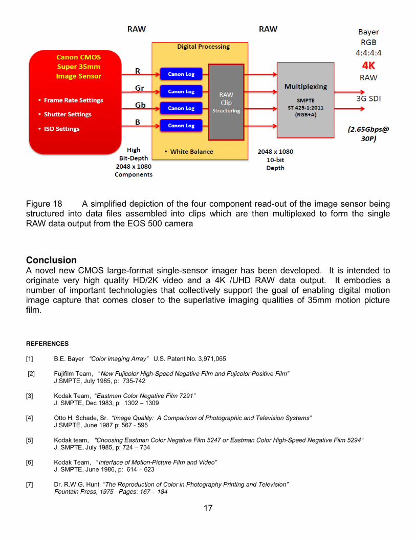
Figure 18 A simplified depiction of the four component read-out of the image sensor being structured into data files assembled into clips which are then multiplexed to form the single RAW data output from the EOS 500 camera
Conclusion A novel new CMOS large-format single-sensor imager has been developed. It is intended to originate very high quality HD/2K video and a 4K /UHD RAW data output. It embodies a number of important technologies that collectively support the goal of enabling digital motion image capture that comes closer to the superlative imaging qualities of 35mm motion picture film.
REFERENCES
[1] B.E. Bayer “Color imaging Array” U.S. Patent No. 3,971,065
[2] Fujifilm Team, “New Fujicolor High-Speed Negative Film and Fujicolor Positive Film” J.SMPTE, July 1985, p: 735-742
[3] Kodak Team, “Eastman Color Negative Film 7291” J. SMPTE, Dec 1983, p: 1302 – 1309
[4] Otto H. Schade, Sr. “Image Quality: A Comparison of Photographic and Television Systems” J.SMPTE, June 1987 p: 567 - 595
[5] Kodak team, “Choosing Eastman Color Negative Film 5247 or Eastman Color High-Speed Negative Film 5294” J. SMPTE, July 1985, p: 724 – 734
[6] Kodak Team, “Interface of Motion-Picture Film and Video” J. SMPTE, June 1986, p: 614 – 623
[7] Dr. R.W.G. Hunt “The Reproduction of Color in Photography Printing and Television” Fountain Press, 1975 Pages: 167 – 184
17