Ultrasonic horn design for ultrasonic machining technologies
Neural Dust: An Ultrasonic, Low Power Solutionfor Chronic Brain-Machine InterfacesDongjin Seo ∗, Jose M. Carmena ∗ †, Jan M. Rabaey ∗ , Elad Alon ∗ ‡, and Michel M. Maharbiz ∗ ‡
∗Department of Electrical Engineering and Computer Sciences and †Helen Wills Neuroscience Institute, University of California, Berkeley, CA, USA‡Joint senior authors
Correspondence to: [email protected]
A major hurdle in brain-machine interfaces (BMI) is the lack ofan implantable neural interface system that remains viable fora lifetime. This paper explores the fundamental system designtrade-offs and ultimate size, power, and bandwidth scaling limitsof neural recording systems built from low-power CMOS circuitrycoupled with ultrasonic power delivery and backscatter commu-nication. In particular, we propose an ultra-miniature as well asextremely compliant system that enables massive scaling in thenumber of neural recordings from the brain while providing a pathtowards truly chronic BMI. These goals are achieved via two fun-damental technology innovations: 1) thousands of 10 – 100 µmscale, free-floating, independent sensor nodes, or neural dust,that detect and report local extracellular electrophysiological data,and 2) a sub-cranial interrogator that establishes power and com-munication links with the neural dust. For 100 µm scale sensingnodes embedded 2 mm into the brain, ultrasonic power transmis-sion can enable 7 % efficiency power links (-11.6 dB), resulting ina received power of ∼500 µW with a 1 mm2 interrogator, whichis >107 more than EM transmission at similar scale (40 pW). Ex-treme efficiency of ultrasonic transmission and CMOS front-endscan enable the scaling of the sensing nodes down to 10’s of µm.
ultrasounic energy harvesting | backscatter communication | chronic extra-cellular recording systems | brain-machine interfaces
Half a century of scientific and engineering effort has yieldeda vast body of knowledge about the brain as well as a set of
tools for stimulating and recording from neurons across multiplebrain structures. However, for clinically relevant applications suchas brain-machine interfaces (BMI), a tetherless, high density, chronicinterface to the brain remains as one of the grand challenges of the21st century.
Currently, the majority of neural recording is done throughthe direct electrical measurement of potential changes near relevantneurons during depolarization events called action potentials (AP).While the specifics vary across several prominent technologies, allof these interfaces share several characteristics: a physical, electricalconnection between the active area inside the brain and electroniccircuits near the periphery (from which, increasingly, data is sentout wirelessly from a "hub") [1–4]; a practical upper bound of sev-eral hundred implantable recording sites [5–8]; and the developmentof a biological response around the implanted electrodes which de-grades recording performance over time [9–12]. To date, chronicclinical neural implants have proved to be successful in the shortrange (months to a few years) and for a small number of channels(10’s to 100’s) [13]. Chronic recording from thousands of sites in aclinically relevant manner with little or no tissue response would bea game changer.
Outside the scope of clinical neuroprosthetics, the need for largescale recording of ensembles of neurons was recently emphasized bythe Brain Research through Advancing Innovative Neurotechnolo-gies (BRAIN) initiative in April 2013 by U.S. President Obama [15]and several related opinion papers [13, 14]. Currently, there are nu-merous modalities with which one can extract information from thebrain. Advances in imaging technologies such as functional magneticresonance imaging (fMRI), electroencephalography (EEG), positron
emission tomography (PET), and magnetoencephalography (MEG)have provided a wealth of information about collective behaviors ofgroups of neurons [16]. Numerous efforts are focusing on intra- [17]and extra-cellular [18] electrophysiological recording and stimula-tion, molecular recording [19], optical recording [20], and hybridtechniques such as opto-genetic stimulation [21] and photo-acoustic[22] methods to perturb and record the individual activity of neu-rons in large (and, hopefully scalable) ensembles. All modalities, ofcourse, have some fundamental tradeoffs and are usually limited intemporal or spatial resolution, portability, power, invasiveness, etc.Note that a comprehensive recent review of tradeoffs focused onrecording from all neurons in a mouse brain can be found in Mar-blestone et al. [23].
System ConceptLow-power CMOS circuits coupled with ultrasonic harvesting andbackscatter communication can provide a toolset from which to buildscalable, chronic extracellular recording systems.
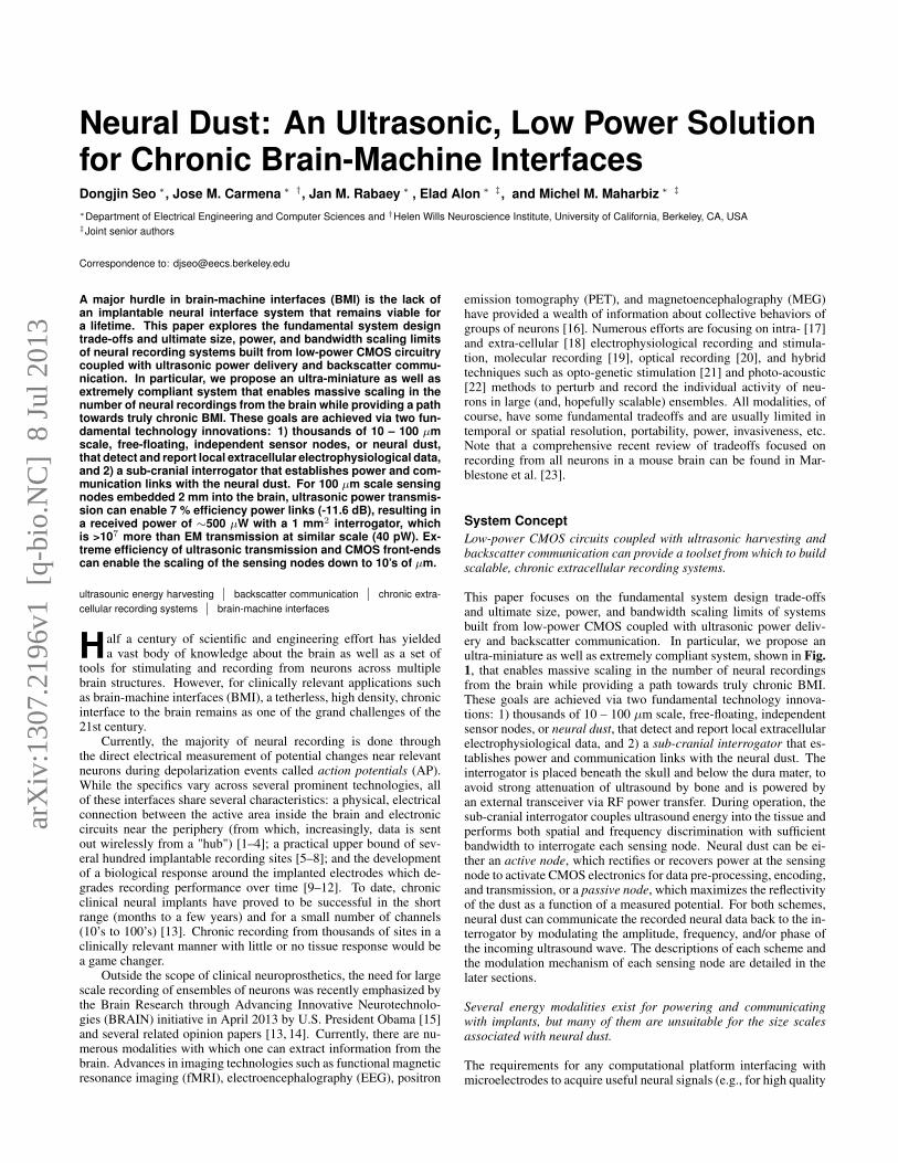
This paper focuses on the fundamental system design trade-offsand ultimate size, power, and bandwidth scaling limits of systemsbuilt from low-power CMOS coupled with ultrasonic power deliv-ery and backscatter communication. In particular, we propose anultra-miniature as well as extremely compliant system, shown in Fig.1, that enables massive scaling in the number of neural recordingsfrom the brain while providing a path towards truly chronic BMI.These goals are achieved via two fundamental technology innova-tions: 1) thousands of 10 – 100 µm scale, free-floating, independentsensor nodes, or neural dust, that detect and report local extracellularelectrophysiological data, and 2) a sub-cranial interrogator that es-tablishes power and communication links with the neural dust. Theinterrogator is placed beneath the skull and below the dura mater, toavoid strong attenuation of ultrasound by bone and is powered byan external transceiver via RF power transfer. During operation, thesub-cranial interrogator couples ultrasound energy into the tissue andperforms both spatial and frequency discrimination with sufficientbandwidth to interrogate each sensing node. Neural dust can be ei-ther an active node, which rectifies or recovers power at the sensingnode to activate CMOS electronics for data pre-processing, encoding,and transmission, or a passive node, which maximizes the reflectivityof the dust as a function of a measured potential. For both schemes,neural dust can communicate the recorded neural data back to the in-terrogator by modulating the amplitude, frequency, and/or phase ofthe incoming ultrasound wave. The descriptions of each scheme andthe modulation mechanism of each sensing node are detailed in thelater sections.
Several energy modalities exist for powering and communicatingwith implants, but many of them are unsuitable for the size scalesassociated with neural dust.
The requirements for any computational platform interfacing withmicroelectrodes to acquire useful neural signals (e.g., for high quality
arX
iv:1
307.
2196
v1 [
q-bi
o.N
C]
8 J
ul 2
013

Fig. 1. Neural dust system diagram showing the placement of ultrasonic inter-rogator under the skull and the independent neural dust sensing nodes dispersedthroughout the brain.
motor control) are fairly stringent [7, 24]. The two primary con-straints on the implanted device are size and power. These are dis-cussed in greater detail below, but we list them briefly next. First,implants placed into cortical tissue with scales larger than one ortwo cell diameters have well-documented tissue responses whichare ultimately detrimental to performance and occur on the time-scale of months [25, 26]. Note that some debate exists as to whatrole mechanical anchoring outside the cortex plays in performancedegradation. Second, all electrical potentials (extra-cellular or oth-erwise) are by definition measured differentially, so as devices scaledown and the distance between recording points decreases accord-ingly, the absolute magnitude of the measured potential will alsodecrease. This decreased amplitude necessitates reductions in thefront-end noise, which in turns requires higher power (i.e., for a fixedbandwidth, lowering the noise floor requires increased power con-sumption). Smaller devices, however, collect less power, and build-ing sufficiently low-power electronics may be extremely challenging.Additionally, to eliminate the risk of infection associated with thetranscutaneous/trans-cranial wires required for communication andpower, such tethers should be avoided as much as possible; a wire-less hub is therefore essential to relay the information recorded bythe device through the skull.
High attenuation in brain tissue and geometry-dependent magneticcoupling limit the transfer efficiency of electromagnetics, especiallyfor miniature implants.
The most popular existing wireless transcutaneous energy transfertechnique relies on electromagnetics (EM) as the energy modal-ity [27]. An external transmitter generates and transfers informationthrough purely electric [28] or magnetic [29] near field or electro-magnetic far field coupling [30]; this energy can be harvested by theimplanted device and converted into a stable DC supply voltage. En-ergy transmission via magnetic near field has been used in a wide va-riety of medical applications and is the principal source of power forcochlear implants [31]. As EM requires no moving parts or the needfor chemical processing or temperature gradients, it is consideredmore robust and stable than other forms energy scavenging. When
Fig. 2. (a) Total channel loss in 2 mm brain tissue, due to both tissue and prop-agation loss, increases exponentially with frequency, resulting in a 20 dB of lossat 10 GHz. (b) The mutual coupling, and therefore link efficiency, also reducesdramatically with the scaling of chiplet dimensions.
used in-body, however, EM coupling power density is restricted bythe potential adverse health effects associated with excess tissue heat-ing in the vicinity of the human body due to electromagnetic fields.This is regulated by the well known FCC and IEEE-recommendedlevels [32]. Roughly, the upper limit for EM power density transitingthrough tissue is set by the minimum required to heat a model sam-ple of human tissue by 1C. For electromagnetic waves, the outputpower density is frequency dependent and cannot exceed a maximumof 10 mW/cm2.
Consider, in this context, the problem of transmitting EM powerto (and information from) very small CMOS chiplets embedded intissue; does this approach scale to allow high density neural record-ings? Regardless of the specific implementation, any such chipletwill contain a resonant component that couples to the EM waves;such a system can be modeled as a series/parallel RLC (for the pur-poses of this exercise, one may presume that a suitable method existsfor modulating the quality factor or mutual coupling of the RLC as afunction of neural activity). Given this, the performance of electro-magnetic power transfer suffers from two fundamental issues. First,the extreme constraint on the size of the node limits the maximumachievable values of the passives. Assuming a planar square loopinductor, calculations predict the resonant frequency of a 100 µmneural dust would be ∼10 GHz. Fig. 2 (a) plots the modeled chan-nel loss, or the attenuation of the EM signal as it propagates through2 mm of brain tissue, due to tissue absorption and beam spreading,as a function of frequency. We observe that there is an exponentialrelationship between the channel loss and the frequency, and at 10GHz – the total combined loss for one-way transmission is approx-imately 20 dB. Moreover, at these very small footprints (comparedto the wavelength, which is in millimeter range), the receive antennaefficiency becomes quite small, thereby easily adding roughly 20 dBof additional loss, resulting in a total gain of at most -40 dB. The tis-sue absorption loss penalty incurred by operating at a high frequencycan be reduced by increasing the capacitance density using 3D inter-digitized capacitor layouts, but even then, as shown in Fig. 2 (b),scaling down the dimensions of the chiplets increases the resonantfrequency of the link, causing an exponential increase in the tissueabsorption loss and the overall channel loss, and the efficiency of EMtransmission becomes miniscule.
To make matters worse, the mutual coupling between the trans-mitter and receiver coils drops dramatically and significantly de-grades the transfer efficiency and increases the sensitivity to mis-
2 Seo, D. et al.

Table 1. Comparison of both the scale and the loss incurred in brain tissuebetween ultrasound and EM radiation, displaying the stark differences in theachievable spatial resolution (set by the wavelength) and the tissue/path lossfor operating frequency of a 100 µm neural dust (*Attenuation of ultrasoundin brain is 0.5 dB/(cm·MHz) [40]).
alignments [33, 34]. As shown in Fig. 2 (b), EM transmission witha 100 µm neural dust embedded 2 mm into the cortex results in 64dB of transmission loss. Given a 1 mm2 transmitter aperture out-putting 100 µW of power – limited by the need to satisfy safetyregulations on output power density of 10 mW/cm2 – the resultingreceived power at the neural dust is ∼40 pW. This is orders of mag-nitude smaller than the power consumption imposed by noise require-ments on the front-end amplification circuitry (refer to later sectionsfor further discussion). As a result, prior work by [1], which featuresthe most energy-efficient and smallest wirelessly EM powered neu-ral recording system to date, at 2.5 µW/channel and 250 µm x 450µm, is limited in terms of further dimensional scaling and increasingthe range (the effective range within brain tissue for this work was 0.6mm). We conclude that due to the non-linear interplay of form factor,speed of light, and frequency spectra of tissue absorption, EM powertransmission is not an appropriate energy modality for the poweringof 10’s of µm sized neural dust implants.
Ultrasound is attractive for in-tissue communication given its shortwavelength and low attenuation.
Ultrasonic transducers have found application in various disciplinesincluding imaging, high intensity focused ultrasound (HIFU), non-destructive testing of materials, communication and power deliv-ery through steel walls, underwater communications, transcutaneouspower delivery, and energy harvesting [35–38]. The idea of us-ing acoustic waves to transmit energy was first proposed in 1958by Rosen [39] to describe the energy coupling between two piezo-electric transducers. Unlike electromagnetics, using ultrasound asan energy transmission modality never entered into widespread con-sumer application and was often overlooked because the efficiency ofelectromagnetics for short distances and large apertures is superior.However, at the scales discussed here and in tissue (i.e., aqueous me-dia) the low acoustic velocity allows operation at dramatically lowerfrequencies, and more importantly, the acoustic loss in tissue is gen-erally substantially smaller than the attenuation of electromagneticsin tissue (Table 1).
As mentioned earlier, the relatively low acoustic velocity of ultra-sound results in substantially reduced wavelength compared to EM.For example, 10 MHz ultrasound in brain tissue has a wavelength λ= 150 µm, while for 10 GHz EM, λ = 5 mm [40]. This smaller wave-length implies that for the same transmission distance, ultrasonic sys-tems are much more likely to operate in the far-field, and hence offermore isotropic characteristics than an EM transmitter (i.e., the ultra-sonic radiator can obtain larger spatial coverage). This opens up theprospect of interrogation of multiple nodes via frequency binning.More importantly, the acoustic loss in brain tissue is fundamentallysmaller than the attenuation of electromagnetics in tissue becauseacoustic transmission relies on compression and rarefaction of thetissue rather than time-varying electric/magnetic fields that gener-ate displacement currents on the surface of the tissue [41]. This isalso manifested by the stark difference in the time-averaged accept-able intensity for ultrasound for cephalic applications, regulated byFDA, which is approximately 9x (94 mW/cm2) for general-purposedevices and 72x (720 mW/cm2) more than EM for devices conform-
ing to output display standards (ODS) (recall EM is limited to 10mW/cm2) [42].
As an aside, in order to increase the instantaneous power cap-tured by an implant, FDA regulations would allow an interrogatorto transmit up to 190 W/cm2 of spatial peak pulse-averaged powerdensity. This approach, however, must be taken with caution asmore in-depth studies of the thermal impact of duty-cycled oper-ation on the tissue are necessary to determine safe parameters ofthe applied duty-cycle and meet the time-averaged power level con-straint [43, 44]. Also, as demonstrated by a body of work investigat-ing the effectiveness of ultrasound as a means of modulating neuronalactivity [45–48], systems operating in this regime may be capable ofmicro-stimulating the brain at a CW time-averaged output intensityas low as 1 W/cm2 [49], and cause tissue ablation through heating andcavitation at intensities in the focal region of 100 - 1000 W/cm2 [50].
Piezoelectric ultrasonic transducers suitable for implanted applica-tions are available.
Piezoelectricity refers to the phenomenon present in certain solid(usually crystalline) materials where there is an interaction betweenthe mechanical and electrical states. As a result, piezoelectric ma-terials can transduce electrical energy into mechanical energy andvice versa by changing lattice structure, and this state change is ac-cessible via either electrical stimulation or mechanical deformation.These materials serve as a critical component in the construction ofprobes that generate ultrasonic waves to enable ultrasound technol-ogy used in the medical industry. A relatively wide range of piezo-electric materials are available, each suitable for different applica-tions. For instance, materials such as single crystal lithium niobate(LiNbO3) and polymer PVDF are excellent choices for fabricatinglarge aperture single element transducers due to their low dielectricpermittivity [51]. On the other hand, a ceramic compound known aslead zirconate titanate (PZT) is a popular choice for high performancediagnostic ultrasonic imaging due to its greater sensitivity, higher op-erational temperature, and exceptional electromechanical couplingcoefficient. The electromechanical coupling coefficient is a figure ofmerit used to describe the ability of a material to convert one form ofenergy into another, and is defined as the ratio of stored mechanicalenergy to total stored energy in a given material. The lead contentof PZT makes it difficult to introduce into human tissue in chronicapplications; several works have demonstrated encapsulation as anoption to avoid this issue [52, 53], but the long-term stability of suchencapsulation layers remain to be investigated.
Luckily, biocompatible piezoelectric materials exist with proper-ties similar (but generally inferior) to PZT; these include barium ti-tanate (BaTiO3), aluminum nitride (AlN) and zinc oxide (ZnO) [54].Although the dielectric coefficients of AlN and ZnO are less thanone-hundredth that of BaTiO3 (which can result in an improvementin the signal to noise ratio due to the lower parallel plate capacitance),their piezoelectric coefficient (which is critical to the link efficiency)is one-tenth that of BaTiO3. Therefore, BaTiO3 transducers are as-sumed for the remainder of the paper. Clearly, material engineeringto synthesize higher performance piezoelectric composite materialsand reliability studies to assess performance over extended periodsof operation are both active areas of research that can significantlycontribute to the realization of neural dust.
System design and constraints: Power DeliveryThere are several implementation strategies for the neural dust. Aneural dust can be an active node, which consists of a piezoelectrictransducer to recover power at the sensing site to activate CMOSelectronics for data pre-processing, encoding, and transmission, or apassive node, which maximizes the reflectivity of the dust as a func-tion of a measured potential. In an active node scheme, the designof neural dust is heavily constrained in both size and available power
Seo, D. et al. 3

to the implant. As a result, it is imperative to accurately model thetransmission channel to maximize the power efficiency. Therefore,this section elaborates design tradeoffs and methodologies for powerdelivery optimization.
The propagation characteristics of ultrasound must be consideredin determining the maximum range of neural dust and the optimaldimension of the external interrogator.
As the pressure field generated by a uniform continuous-wave ex-cited piezoelectric transducer propagates through the tissue medium,the characteristics of the pressure field change with distance from thesource. The varying field is typically divided into two segments, nearfield and far field. In the near field, the shape of the pressure field iscylindrical and the envelope of the field oscillates. At some pointdistal to the transducer, however, the beam begins to diverge and thepressure field becomes a spherically spreading wave, which decaysinversely with distance. The transition between the near and far fieldis where the pressure field converges to a natural focus, and the dis-tance at which this occurs is called the Rayleigh distance, definedas,
L =(D2 − λ2)
4λ≈ D2
4λ,D2 λ2 [1]
where D is the aperture width of the transmitter and λ is the wave-length of ultrasound in the propagation medium. In order to maxi-mize the received power, it is preferable to place the receiver at oneRayleigh distance where the beam spreading is at a minimum. There-fore, with 2 mm of transmission distance and a resonant frequencyof 10 MHz (λ = 150 µm), the maximum dimension of the externalinterrogator should be ∼1 mm.
Neural dust transducers can be simulated with finite element pack-ages and incorporated into a KLM-based link model.
Due to the importance of piezoelectric transducers in various appli-cations, a number of models of the electromechanical operation ofone-dimensional piezoelectric and acoustic phenomena have evolvedover the years. The KLM model is arguably the most common equiv-alent circuit and is a useful starting point to construct a full link modelwith the intent of examining scaling and system constraints [55]. Thebasic model includes a piezoelectric transducer with electrodes fullycovering the two largest faces of the transducer. The entire transduceris modeled as a frequency-dependent three-port network, consistingof one electrical port (where electric power is applied or collected)and two acoustical ports (where mechanical waves are produced orsensed from the front and back faces of the transducer). The parallel-plate capacitance due to the electrodes and the frequency-dependentacoustic capacitance are modeled as C and Xi, respectively, and thetransduction between electrical and mechanical domains is modeledas an ideal electromechanical transformer with a turn ratio of Φ, con-nected to the middle of a transmission line of length λ/2, as shownin Fig. 3. Assuming an infinite 2D plate piezoelectric transducer ofthickness h, the resonant frequency is set by h = λ/2; at the resonantfrequency, the ultrasound wave impinging on either the front or backface of the transducer will undergo a 180 phase shift to reach theother side, causing the largest displacement between the two faces.This observation implies that phase inversion only exists at the oddharmonics of the fundamental mode in a given geometry.
The KLM model, however, was derived under the assumptionof pure one-dimensional thickness vibration, and therefore can onlyprovide a valid representation for a piezoelectric transducer with anaspect ratio (width/thickness) greater than 10 that mainly resonatesin the thickness mode [56]. Given the extreme miniaturization tar-get for the neural dust, a cube dimension (aspect ratio of 1:1:1) isa better approximation of the geometry than a plate (aspect ratio >
Fig. 3. KLM model of a neural dust piezoelectric transducer, showing one elec-trical port and two mechanical ports. Coupling between the domains is modeledwith an ideal electromechanical transformer.
10:10:1). Due to Poisson’s ratio and the associated mode couplingbetween resonant modes along each of the three axes of the cube,changing aspect ratio alters the resonant frequencies [57]. The piezo-electric transducers for both the interrogator and the neural dust mustbe designed to resonate at the same frequency to maximize the linkefficiency. In the model below, we assume the neural dust nodes arecubic and the external transceiver is approximately planar (i.e., 2D)so care must be taken not to confuse the thickness of the interrogatorand the neural dust.
In order to obtain KLM parameters for the neural dust transducer,we simulated a cube transducer using a 3D finite element package(COMSOL Multiphysics) to model both the resonant frequency shiftvs. a plate and the manifestation of spurious tones and higher reso-nances. The effect of resonance shift is included in the KLM modelby extracting the effective acoustic impedance of the neural dust fromthe COMSOL model. To match the resonant frequency of the inter-rogator and the neural dust, the interrogator thickness is varied tomatch the fundamental thickness mode of the neural dust. Approxi-mately 66 % of the total output energy is contained in the main thick-ness resonance; this is modeled as a loss term. Coupling into othermodes, however, can be reduced by stretching BaTiO3 in the [110]direction because BaTiO3 is both anisotropic and partially auxetic,exhibiting negative Poisson’s ratio and therefore providing gain whenstretched [58, 59]. Well-engineered placement of electrodes may en-able orientation-insensitive implant nodes and can allow multi-nodead-hoc type communication networks. More on this topic will beelaborated in the discussion section.
The maximum energy transfer efficiency can be found via a link modelconsisting of a cascade of two-port networks.
A good model of the ultrasonic channel is crucial in order to as-sess the tradeoffs in optimizing systems for energy transfer throughlossy brain tissue. The complete energy link model is shown in Fig.4 and can be divided into three parts: (1) the ultrasonic interrogatoror transmitter, (2) tissue, and (3) the neural dust or receiver. A sig-nal generator and amplifying stages produce power for the ultrasonictransmitter through an impedance matching circuit that provides con-jugate matching at the input. The ultrasonic wave launched by theinterrogator penetrates brain tissue, modeled as a lossy transmissionline, and a fraction of that energy is harvested by the ultrasonic re-ceiver, or neural dust. We evaluated embedding the receiver up to2 mm into the tissue, which generates an AC voltage at the electri-cal port of the piezoelectric transducer in response to the incomingultrasonic energy.
In order to compute the link energy transfer efficiency, the modelcan be decomposed to a set of linear and time-invariant two-port pa-rameters, representing a linear relationship between the input andoutput voltage. Here, we choose to represent the input-to-output re-lationship using ABCD parameters, which simplify analysis of cas-cades of two-port networks through simple matrix multiplication.By representing the link model with the two-port network, we cancome to conclusions concerning optimal power transfer efficiency (or"gain").
4 Seo, D. et al.

Generally, maximum link efficiency (Gmax) is achieved whenwe can conjugate match both the input and the output of a two-port network. However, with a 100 µm neural dust node, the outputimpedance level is such that it would require∼100 µH of inductanceto perfectly conjugate match the output of the two port link network.Given the compact form factor of the neural dust, it is completelyinfeasible to obtain such inductance with electrical means, and there-fore Gmax is an unachievable figure of merit. It may be possible toapproach Gmax by mechanical means such as the addition of ma-terial layers that perform an acoustic impedance transformation, orsimilarly, by electromechanical means such as utilizing microma-chined acoustic resonators. We do not explore the first option indetail as it would likely lead to thickness increases on order of in-teger fractions of a wavelength (but see Fig. 5 (b) and below); thesecond option is touched upon in Discussion and Conclusion. There-fore, for comparison and scaling analysis, we assume we only haveimpedance control at the input, or the interrogator side, and therefore,power gain (Gp) is the suitable figure-of-merit.
For a 100 µm node embedded 2 mm into the brain, ultrasonic powertransmission can enable 7 % efficiency power links (-11.6 dB), re-sulting in a received power of ∼500 µW with a 1 mm2 interrogator.
The complete link model is implemented in MATLAB with the lim-itations of the KLM model (as outlined in the previous section) cor-rected via COMSOL simulations. Given a 1 mm2 interrogator, Fig.5 plots both the efficiency of the link and the received power at thesensor node as the size of the dust node scales and the thickness of theinterrogating transducer is adjusted to match the resonant frequencyof the dust node and the tissue (i.e., transmission line resonator). Wenote that the maximum efficiency of the KLM-adapted link model,where the interrogator is fully immersed in the tissue medium, is lim-ited to 50 % because both the back and front side of the interrogatorare loaded by the tissue layer. This results in an efficiency drop of 3dB as the ultrasonic energy couples to both the front and back face ofthe transducer equally. Additionally, without any impedance match-ing, since the acoustic impedance of the tissue (1.5 MRayls) and thatof BaTiO3 (30 MRayls) are drastically different, significant reflectionoccurs at their boundaries. Depending on the thickness of neural dustand the resonant frequency of the network, ultrasonic waves launchedby the interrogator undergo varying phase changes through the lossytissue. Thus, the efficiency of a system with smaller dust nodes canbe improved if the total propagation distance happens to be a multipleof a wavelength of the ultrasound. As a result, for dust nodes greaterthan 100 µm, we note that the efficiency does not monotonically in-crease with the dimension. On the other hand, for a dust node that
Fig. 4. Complete single interrogator, single neural dust power and communica-tion through link models.
is less than 100 µm in dimension, because the wavelength associatedwith the network’s resonant frequency is much smaller than its tissuepropagation distance, the link efficiency depends more heavily on thecross-sectional area of the neural dust. Therefore, we note that theefficiency will drop at least quadratically with the reduction of neuraldust dimension. The efficiency of the link can be improved with aλ/4 matching layer for impedance transformation, but the improve-ment is limited due to the loss from the material (e.g., attenuation ofgraphite epoxy is ∼16 dB/(cm·MHz) [60] compared to that in braintissue which is 0.5 dB/(cm·MHz) [40]) as shown in Fig. 5 (b). Notethat for the case with this matching layer, the efficiency is worse fordust nodes that are >500 µm since the loss of the matching layeroutweighs that of the tissue.
More specifically, simulation of the complete link indicates thatfor a 100 µm node embedded 2 mm into the brain, ultrasonic powertransmission can enable 7 % efficiency power transmission (-11.6dB). As shown in Fig. 5 (a), the optimal transmission frequency is 8MHz; half of this peak Gp can be maintained for carrier frequenciesthat are±2 MHz separated from this peak. At the resonant frequency,we can receive up to ∼500 µW at the neural dust node (resulting innano-meters of total displacement) with a 1 mm2 interrogator, whichis >107 more than EM transmission at the same size scale (40 pW inFig. 2). Scaling of neural dust also indicates that approximately 3.5µW can be recovered by a dust node as small as 20 µm through ultra-sonic transmission, which is still in the realm of feasibility to operatea state-of-the-art CMOS neural front-end. Designing an ultra-energyefficient neural front-end in CMOS in such small footprint (20 µmx 20 µm), however, is an extremely challenging problem and is dis-cussed in detail below.
System design and constraints: Sensing / CommunicationExtracting neural potential recording from a noisy environment is achallenging problem.
The electrical activity of neurons is most directly measured as anelectrical potential across the cellular membrane. As a result, thehighest fidelity measurement can be achieved using patch-clampmethods, where a glass pipette is placed in the vicinity of the cell andan intra-cellular electrical connection is established by penetratingthe cellular membrane and sealing the membrane around the pipette.While this approach is well studied and commonly practiced, it doesnot scale well and is currently not useful for chronic implants due to
Fig. 5. (a) Ultrasonic power transfer efficiency vs. operating frequency for a 100µm neural dust (b) Link efficiency with and without a matching layer as a functionof the neural dust side dimension.
Seo, D. et al. 5

the complexity of the procedure (but see [61–63]). Due to these lim-itations, clinically-relevant, implantable recordings are taken extra-cellularly; that is, electrical measurements are taken entirely outsidethe cells.
A typical extracellular electrophysiological recording of neuralactivity in tissue usually records electrical potential differences be-tween one electrode placed in-tissue near the neural activity and asecond electrode "far away" which acts as a global ground or counterelectrode (depending on the configuration). The recorded signal con-sists of three components: an electrochemical offset that appears asa DC offset, typically in the range of 100’s of mV, low-frequency(0.1 – 600 Hz) changes [64] (∼0.5 mV amplitude) often termedlocal field potential (LFP) from a spatial average of neural activ-ity in the neighborhood of electrodes and high frequency (0.8 – 10kHz) action potential (AP) or spiking events (∼100 µV) associatedwith the discharge of individual neurons in the vicinity of the elec-trode [6]. Ignoring noise inherent in the recording equipment (whichis usually not insubstantial), there are two main sources of corti-cal recording noise: thermal noise generated by the recording elec-trode and the tissue interface and biological interference which arisesfrom asynchronous neural activity in close proximity to the recordingsite. Therefore, neural signal acquisition chains often rely on obtain-ing a maximum signal level at the front-ends and/or separating theµV-level desired signal from large offsets and low frequency distur-bances.
Spatial separation of recording electrodes to maximize the achiev-able differential signal on neural dust is the bottleneck for scaling.
Free-floating extracellular recording at untethered, ultra-small dustnodes poses a major challenge in scaling. Unlike the needle-like mi-croelectrode shanks that can measure time-domain electrical poten-tial at each recording site in relation to a common electrode, placedrelatively far away, both the recording and the common electrodemust be placed within the same (very small) footprint. Although thetwo are interchangeable, the separation and therefore, the maximumdifferential signal between the electrodes are inherently limited bythe neural dust footprint, and follow the dipole-dipole voltage char-acteristic that decreases quadratically (unless very near a cell body, inwhich case it appears to scale exponentially; see [65] for a more thor-ough review) with increasing separation distance. Since the poweravailable to the implant has a fixed upper bound (see above), the re-duction of extracellular potential amplitude as the neural dust dimen-sions are scaled down in the presence of biological, thermal, elec-tronic, and mechanical noise (which do not scale), causes the signal-to-noise (SNR) ratio to degrade significantly; this places heavy con-straints on the CMOS front-ends for processing and extracting thesignal from extremely noisy measurements. Therefore, if we con-sider sufficient SNR at the input of the neural front-ends as one of thedesign variables, the scaling of neural dust (as depicted in Fig. 5 (b))must be revisited.
Careful co-optimization of piezoelectric transducer and CMOS front-end circuitry can push the operation of neural dust down at least tothe 50 µm scale.
Focusing specifically on the scaling of a cubic neural dust, we runinto the inherent limitation in the maximum achievable differentialsignal (discussed above). At a separation distance of 100 µm betweenrecording electrodes, we expect a 10 µV AP amplitude [data derivedfrom [66]], with the amplitude further reducing quadratically as theseparation is reduced. Since the power available to the neural dust islimited, the design goal of a front-end architecture is to minimize theinput-referred noise within this power budget. The power efficiencyfactor (NEF2 · Vdd) quantifies the tradeoff between power and noise[24] and extrapolating from the measurement result of a previousCMOS neural front-end design (NEF2 · Vdd of 9.42 [1]), we can es-
Fig. 6. As we scale down the neural dust size, more power is needed to keep thenoise floor down to maintain SNR while less power is captured. The intersectionof these two trends is the smallest node that will still operate. Scaling with anSNR of 3 shows operation down to 50 µm. The analysis assumes the use ofBaTiO3, two different FDA-approved ultrasonic energy transfer protocols, anddoes not include the use of matching layers.
timate the relationship between the input-referred noise level and theDC power consumption of an optimally designed front-end architec-ture as we scale. The fundamental limit to the NEF2 ·Vdd occurs at asupply voltage of at least ∼4 kBT/q or 100 mV, in order to reliablyoperate the FET, and by definition, the NEF of 1 for a single BJT am-plifier [67]. In principle, one could push the supply voltage down to∼2 kBT/q, but in practice 100 mV is already extremely aggressive.
Fixing the input SNR to 3, which should be sufficient for extract-ing neural signals, we can evaluate the scaling capability of neuraldust as shown in Fig. 6. We assumed the use of BaTiO3 in the modeldescribed in the section above and do not include the use of matchinglayers. We also assumed that the interrogator’s output power is con-strained by the two different FDA-approved ultrasonic energy trans-fer protocols. We note that there exists an inherent tradeoff betweenthe power available to the implant and the exponential increase in thepower required to achieve an SNR of 3 with the reduction of spacingbetween the electrodes. The point of intersection in Fig. 6 denotes theminimum size of neural dust that enables the operation of the com-plete link. For the stated assumptions, this occurs at 50 µm, which isgreater than the dimension at which the thermal noise from the elec-trode (R = 20 kΩ and BW = 10 kHz) limits further scaling. This ef-fectively means that, staying within FDA-approved ultrasound powerlimits, assuming an SNR of 3 is required, neural dust nodes smallerthan 50 µm cannot receive enough power to distinguish neural activ-ity from noise. Note that the cross-over assumes 100 % efficiency inthe rectifier and zero overhead cost in the remaining circuitry, bothof which will not be true in practice (i.e., the actual size limit will belarger than this).
Given the lower size limit for scaling these systems, as well asthe need to implant them entirely in the cortex, both wireless powerand communication schemes are required for the neural dust nodes.The communication strategy is detailed below.
Neural electrophysiological data can be reported back via backscat-tering – i.e., modulating reflection of the incident carrier.
Radio frequency identification (RFID) technologies have found broadadoption in the past decade, and were made possible by advancesin wireless powering techniques as well as the improved energy-efficiency of the computational substrates. In general, RFID em-
6 Seo, D. et al.
ploys two different mechanisms to communicate with sensor tags:active and passive [68]. When queried, active tags, which are battery-powered and contain a low power radio like conventional wireless de-vices, internally generate electromagnetic radiation in order to trans-mit the data back to the reader. In contrast, passive and semi-passivetags transmit data by modulating the incoming RF energy and re-radiating the modulated RF energy back to the reader, a methodcalled backscattering. Modulation of the backscattered RF energycan be achieved by varying the load impedance, which changes thecoefficient of reflectivity. Furthermore, backscattering is amenableto parallel communication among sensor tags and one interrogatordistinguishing among different receivers by using frequency diver-sity [69]. Multi-mode strategies are discussed in Discussion and Con-clusion.
For the ultra-miniature, chronic implants discussed here (whichhave stringent requirements on both the size and power available tothe implant), broadcasting the information back to the interrogatorvia backscattering is a more attractive choice than building a fullyactive transmitter on the implant. As a passive device, backscatteringreceivers do not need batteries or significant capacitive energy stor-age, thus extending lifetimes, eliminating the risk of battery leakage,and removing the significant impediment to size scaling that wouldbe created by the dramatically reduced capacitance available on asmall node. The powering and communication strategies developedfor electromagnetic backscattering can be applied to any link, regard-less of the transmission channel modality (i.e., ultrasound).
Co-integration of CMOS and piezoelectric transducer is challenging,but CMOS can provide dynamic control over the load impedance.
The CMOS component of an active neural dust node must at leastconsist of a full-wave bridge rectifier to convert the harvested piezo-electric AC signal to a DC level and regulators to generate a stableand appropriate DC supply voltage for the rest of the CMOS circuitry.The basic architecture of the CMOS front-ends will depend on theapplication. For the acquisition of the entire neural signal trace, wemust capture both the LFP and action potentials. Given the relativeamplitude, DC offset, and frequency range of these signals, the cir-cuit must operate at a full bandwidth of 0 to 10 kHz with >70 dB ofinput dynamic range [24]. Researchers have demonstrated a mixed-signal data acquisition architecture solution to extract LFP and actionpotentials, originally proposed in [24], which cancels the DC offsetin the analog domain to alleviate the dynamic range constraints andto eliminate bulky passive components used in [70, 71]. Therefore,the CMOS front-ends include rectifiers, voltage regulators, low-noiseamplifiers, DC-coupled analog-to-digital converters (ADC) and mod-
ulators to communicate the decoded information back to the inter-rogator.
Co-integration and packaging challenges and – most importantly– the footprint of current CMOS neural front-ends present majorroadblocks to the active implant approach. The smallest CMOSneural front-end system published to date, not including rectifiersand modulators, occupies approximately 100 µm2 of silicon real es-tate [24], and packing the same functionality onto a smaller foot-print may not be plausible. Thinned, multi-substrate integration tomeet the volume requirements while keeping the overall CMOS areaconstant may resolve this issue, but requires substantial further tech-nology development to represent a viable solution. Scaling the ac-tive electronics to appropriate dimensions is clearly a bottleneck, butpresents an enticing opportunity for further innovation to address theissue.
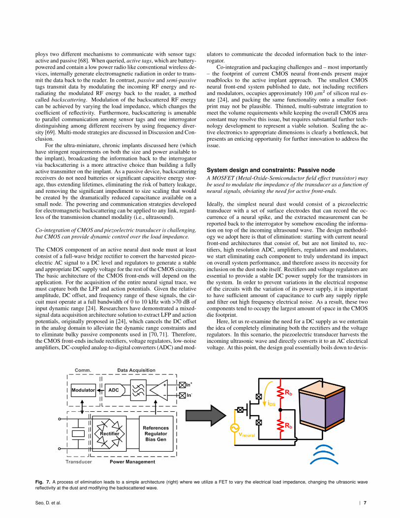
System design and constraints: Passive nodeA MOSFET (Metal-Oxide-Semiconductor field effect transistor) maybe used to modulate the impedance of the transducer as a function ofneural signals, obviating the need for active front-ends.
Ideally, the simplest neural dust would consist of a piezoelectrictransducer with a set of surface electrodes that can record the oc-currence of a neural spike, and the extracted measurement can bereported back to the interrogator by somehow encoding the informa-tion on top of the incoming ultrasound wave. The design methodol-ogy we adopt here is that of elimination: starting with current neuralfront-end architectures that consist of, but are not limited to, rec-tifiers, high resolution ADC, amplifiers, regulators and modulators,we start eliminating each component to truly understand its impacton overall system performance, and therefore assess its necessity forinclusion on the dust node itself. Rectifiers and voltage regulators areessential to provide a stable DC power supply for the transistors inthe system. In order to prevent variations in the electrical responseof the circuits with the variation of its power supply, it is importantto have sufficient amount of capacitance to curb any supply rippleand filter out high frequency electrical noise. As a result, these twocomponents tend to occupy the largest amount of space in the CMOSdie footprint.
Here, let us re-examine the need for a DC supply as we entertainthe idea of completely eliminating both the rectifiers and the voltageregulators. In this scenario, the piezoelectric transducer harvests theincoming ultrasonic wave and directly converts it to an AC electricalvoltage. At this point, the design goal essentially boils down to devis-
Fig. 7. A process of elimination leads to a simple architecture (right) where we utilize a FET to vary the electrical load impedance, changing the ultrasonic wavereflectivity at the dust and modifying the backscattered wave.
Seo, D. et al. 7

ing ways of encoding neural data on top of this incoming ultrasoundwave, to be reported back to the interrogator via modulation.
We propose a method outlined in Fig. 7, where the drain (D)and source (S) of a single FET sensor are connected to the two termi-nals of a piezoelectric transducer while the FET modulates the cur-rent IDS as a function of a gate (G) to source voltage, VGS . In thisscheme, given that the supplied VDS of the FET is an AC voltage thatswings both positive and negative, the body (B) of the FET must bebiased carefully. Normally, for an NFET, the body is connected to thesource voltage to prevent the diode at the B-S and B-D junctions fromturning on. However, keep in mind that since a FET is a symmetricdevice, the source and drain are defined only by which terminal is ata lower potential. Therefore, the electrical source/drain terminals, orleft/right for disambiguation (from a cross section of MOS device),swap physical sides every half cycle of the harvested AC waveform.As a result, simply shorting the body to either physical terminal ofthe FET causes the diode formed at the B-S and B-D junctions tobe forward-biased, so care must be taken to avoid neural signal frommodulating the incoming sinusoid only half of the cycle.
As a result, we propose an alternative biasing scheme for the FETto modulate the entire sinusoid as shown in Fig. 7. The resistors Rb
act to cause the neural potential to appear between the gate and bothof the left/right terminals of the transistors while superimposing theAC waveform from the ultrasonic transducer across these same twoterminals. In this manner, even though the electrical source/drain ter-minals swap every half cycle, during both halves of the cycle the VGS
of the FET is modulated by the neural signal.The circuit achieves this superposition by relying on the fact
that the neural signals occupy a much lower frequency band thanthe ultrasound, and that the ultrasound transducer itself has a capac-itive output impedance (Cpiezo). Thus, Rb should be chosen so that1/(Rb · Cpiezo) is placed well above the bandwidth of Vneural (>10kHz) but well below the ultrasound frequency (∼10 MHz for a 100µm node). Rb along with the transistor width must also be chosencarefully to achieve the best reflectivity, as will be described shortly.
Since modulation of IDS in turn modulates the impedance seenacross the two piezoelectric drive terminals, the FET effectively mod-ulates the backscattered signal seen by a distant transmitter. Thechange in the nominal level of IDS is a function of VGS , which canbe up to 10 µV (Vneural) for a 100 µm dust node near an active neu-ron. The sensitivity, S, to the action potential, then, is defined as thechange in IDS with respect to VGS normalized by the nominal IDS
(in addition to the current through Rb) and Vneural,
S =Vneural
IDS + VDS/2Rb· ∂IDS
∂VGS= Vneural ·
gmIDS + VDS/2Rb
[2]
Since gm (transconductance of a FET) is directly proportional toIDS , in order to maximize gm/IDS (i.e., achieves the largest gm fora given IDS), we would like to operate the FET in its steepest region– specifically, deep sub-threshold where it looks like a bipolar junc-tion transistor (BJT). Therefore, the nominal VGS bias can be 0 V,which simplifies the bias circuitry. The modulation of the current isequivalent to a change in the effective impedance of the FET, or theelectrical load to the piezoelectric transducer. This variation in theload impedance affects the ultrasonic wave reflectivity at the neuraldust and modifies the wave that is backscattered. Note that in or-der to maximize the sensitivity (i.e., operating the transistor in deepsub-threshold), the system should be constrained such that the piezo-electric voltage is never too large compared to the threshold voltage.
A SPICE simulation of a typical low-threshold voltage NFET ina standard 65 nm CMOS technology was used in order to assess thenominal current level and the change in the effective impedance ofthe electrical load with Vneural. We assumed that we can implementsuitably large Rb in sufficiently small area of the neural dust nodes.As previously mentioned, in deep sub-threshold, the FET behaves asa BJT, where the physical limit on the achievable gm/IDS = q/kBT ,
determined by the Boltzmann distribution of carriers. As a result, wecan obtain S = 400 ppm for Vneural = 10 µV with a perfect BJT.Given the non-ideality factors associated with FETs, the sensitivityis reduced by a factor of 1.5 – 2, to roughly 250 ppm, which is con-firmed by the simulation.
The implication of the modification in the electrical properties ofthe NFET (output load of the piezoelectric transducer) on the changein the acoustic signal and the corresponding design specifications forthe interrogator is discussed in detail below.
System design and constraints: InterrogatorShorter transmission distance and larger aperture of the interrogatorallow efficient trans-cranial power delivery via electromagnetics.
The focus of the paper up to this point has been on the constraintsassociated with scaling the neural dust. In order to interface with theBMI electronics and to post-process recorded neural data for brainmapping, an interrogator that can extract the information of the sen-sor nodes, perform precise localization and addressing, and providepower for the communication needs to be designed. To achieve aBMI-relevant density of neural recordings, neural dust implants mayneed to be spaced as close as 100 µm (embedded up to a depth of2 mm into the cortex). On the other hand, the interrogator elementswill be larger than the sensor nodes and will be spaced at a largerpitch (between 100 µm and 1 mm). Furthermore, for the prelimi-nary system, we assume that the interrogator is placed beneath theskull and below the dura mater, to avoid strong attenuation of ultra-sound by bone (∼22 dB/(cm·MHz) [40]) and to prevent wave reflec-tion and efficiency loss from impedance mismatch between differenttissue layers and the skull. The complete trans-cranial transmittersystem then would nominally contain an EM link to couple infor-mation through the skull [72]. We do not discuss the design of theRF trans-cranial communication link as that is covered in other work.
Sufficient receiver sensitivity is required by the interrogator to re-solve the occurrence of a neural spike.
A different set of challenges exist in implementing circuitry to gener-ate, collect and process neural data. Namely, innovative approachesare essential to 1) ensure that the interrogator/sensor combinationhas sufficient sensitivity to meet the necessary data resolution forBMI and 2) allow for combination of various multi-node interroga-tion strategies to distinguish among different sensor nodes.
For the analysis carried out in this paper, we assumed that thepower and size constraints of the neural dust, and not the interroga-tor, are the major bottlenecks in the scaling of ultrasound-mediatedneural dust system. In order to verify the validity of this assumption,we can examine, to the zeroth order, the power required by the inter-rogator to achieve certain receiver sensitivity for a passive implemen-tation of the neural dust node. From the complete link model shownin Fig. 4, we note that the change in the electrical impedance of theNFET load induces a change in the input admittance (or the inputpower) of the two-port network. The interrogator (receiver) must beable to detect this change in the input power level in order to resolvethe occurrence of a neural spike. Therefore, we need to determine thesize of the FET sensor on the dust node that maximizes the change inthe input power level of the two-port network, or,
∆Pin ∝∣∣∣∣Yin,spike − Yin,nom
Yin,nom
∣∣∣∣ [3]
where Yin,spike and Yin,nom denote input admittance of the two-portnetwork with and without a neural spike, respectively. Fig. 8 showsthe result of the optimization problem with a standard 65 nm CMOStechnology. For 100 µm and 20 µm dust nodes, 75 µm and 16 µmwidth FET maximize ∆Pin, respectively. Note that since the op-timum transistor width (i.e., nominal impedance) for achieving the
8 Seo, D. et al.

Fig. 8. Change in the input power level (i.e., power at the interrogator) as afunction of transistors width for a 65nm CMOS process and with (a) 100 µm and(b) 20 µm neural dust nodes.
largest reflection is pretty flat, passive node is insensitive to the ef-fects of threshold variability in the transistors and DC offsets in theneural electrodes.
The FET sensor design variable (transistor width), however, isconstrained due to the thermal noise of the FET (which sets the lowerlimit) and the maximum available power at the node and the neuraldust form factor (which set the upper limits). Clearly, the small foot-print of the neural dust restricts the maximum effective width of theFET sensor that we can pack on the dust, and we term this the arealimit. More importantly, we need to ensure that the thermal voltagenoise of the FET does not overwhelm the AP voltage. As a result,for a fixed bandwidth, in order to lower this voltage noise floor of theFET, it is necessary to increase the bias current, and hence the powerconsumption given a fixed output voltage. Given a simple single-ended transistor amplifier with a single dominant pole, a bias currentof IDS , and a transconductance of gm, the minimum bias currentrequired can be derived as,
IDS =π
4· 4kBT
v2n· kBT
q·BW [4]
where v2n is the input-referred voltage noise. As a result, the FETmust be large enough to be able to sustain this minimum bias cur-rent. Therefore, for a BW = 10 kHz and voltage SNR at the inputof the FET of 3 (which sets v2n based on Vneural), we can computethe minimum allowable size of the FET, restricted by the noise limit.Finally, in order to reliably operate the FET, the drain-source voltageof the FET must be at least∼4 kBT/q or 100 mV. As a result, neuraldust must capture enough power from the interrogator to sustain both100 mV and the minimum current required to ensure that the thermalnoise does not dominate the AP voltage. This is defined as the powerlimit.
With such restrictions, Fig. 8 shows that for a 100 µm dust node,we can design a FET sensor to generate a 16.6 ppm change in theinput power with a measured Vneural. This results in ∼120 nW (-39dBm) of backscattered power at the input given a 1 mm2 interroga-tor aperture outputting 7.2 mW of power to satisfy safety regulationson output power density of 720 mW/cm2. With such power levels,given a thermal noise spectral density of -174 dBm/Hz of input noisepower, 10 kHz of BW, 10 dB of noise figure, and 10 dB of SNR,a traditional CMOS receiver should be sensitive enough to detect atminimum -114 dBm of input power. A number of highly-sensitivity
Fig. 9. Neural dust with an ultra-compliant flexible polyimide "tail", populatedwith recording sites, can be envisioned to bypass the limits of the achievabledifferential signal between two electrodes placed on a neural dust footprint.
receivers with < mW of DC power consumption have been demon-strated (e.g., [73]).
For a 20 µm dust, however, Fig. 8 shows that the upper limit onthe FET size imposed by the power limit is lower than the lower limitset by the noise limit, indicating that the passive implementation ofneural dust system scales roughly to 20 µm.
Re-design of neural dust nodeThe scaling of both active and passive node implementations pre-sented above is limited by the noise requirement of the front-end ar-chitectures, which is determined by the achievable differential signalsbetween the electrodes. Decoupling the inherent tradeoff between thesize of individual implants and the achievable SNR can improve thescaling of these implementations.
Re-thinking the design of neural dust can enhance its scalability.
Since the trade-off derives directly not from the neural dust dimen-sion, but from electrode separation, one approach may be to add verysmall footprint (∼1 – 5 µm wide) "tails" which position a single (ormultiple) electrode relatively far (> 50 – 100 µm) from the base ofthe neural dust implant. This would result in the design shown inFig. 9, where instead of placing a single differential surface elec-trode on neural dust, the neural dust can consist of a short strand offlexible and ultra-compliant substrate populated with recording sites.Assuming that the achievable electrode separation in the tail of a 20µm node is 100 µm, this implies that the noise limit, as shown in Fig.8, will set the lower bound to 0.4 µm of transistor width and allowthe design of a FET sensor on the dust node that achieves the opti-mal sensitivity, at 2.3e-3 ppm. This corresponds to 16.6 pW (-77.8dBm) of backscattered power at the input, which is still in the realmof feasibility with a traditional CMOS receiver [73]. Therefore, thisapproach can address one of the major pitfalls with only a minor ad-justment to the original idea as this neural dust still operates underthe same principle as before, but has higher achievable SNR.
Note that the exact technology used for the previous analysis isnot critical to the conclusion we drew. Although the absolute valueof the impedance level is important since it determines the reflectioncoefficient, and therefore, the efficacy of the backscatter, as shown inFig. 8, the analysis above indicates that the optimal transistor widthfor the maximal sensitivity is small compared to the available neu-ral dust footprint. Therefore, although the threshold voltage (hencethe nominal impedance level per transistor width) may vary amongdifferent technology nodes, achieving the optimal impedance levelwithin the footprint may not be an issue.
In addition, since the analysis above does not take into accountsadditional interference (e.g., ultrasonic wave reflection from otherstructures in the brain, such as vasculature), the sensitivity require-ment of the interrogator are more stringent than predicted earlier.
Seo, D. et al. 9

Such reflections will likely lead to intersymbol interference. In thecase of an active node, such interference can be dealt with throughadaptive equalization and/or error correcting codes [74]. For the pas-sive system – which is effectively "transmitting" analog informationback to the interrogator through the backscatter – some form of fil-tering could be applied to reverse the effects of these reflections.Alternatively, one could potentially utilize a pulse-based system touniquely discriminate the various reflections based on their arrivaltimes.
Discussion and ConclusionsThe analysis presented points to three major challenges in the realiza-tion of ultra-small, ultrasound-based neural recording systems. Thefirst is the design and demonstration of front-ends suitable for op-erating within the extreme constraints of decreasing available powerand decreasing SNR with scale. This could be addressed with a com-bination of CMOS process and design innovation as well as thinned,multi-substrate integration strategies (see, for example, [75,76]). Thesecond challenge is the integration of extremely small piezoelectrictransducers and CMOS electronics in a properly encapsulated pack-age. The above discussion assumed the entire neural dust implantwas encapsulated in an inert polymer or insulator film (a variety ofsuch coatings are used routinely in neural recording devices; these in-clude parylene, polyimide, silicon nitride and silicon dioxide, amongothers) while exposing two recording electrodes to the brain. Theaddition of "tails" as discussed above presents additional fabricationchallenges. The third challenge arises in the design and implementa-tion of suitably sensitive sub-cranial transceivers which can operateat low power (to avoid heating between skull and brain). In additionto these three challenges, this paper does not discuss how to deliverneural dust nodes into the cortex. The most direct approach would beto implant them at the tips of fine-wire arrays similar to those alreadyused for neural recording. Neural dust nodes would be fabricated orpost-fab assembled on the tips of array shanks, held there by surfacetension or resorbable layers; a recent result demonstrates a similarapproach to implant untethered LEDs into neural tissue [77]. Once
inserted and free, the array shanks would be withdrawn, allowing thetissue to heal. Kinetic delivery might also be an option, but there isno existing data to evaluate what effect such a method would have onbrain tissue or the devices themselves.
The trans-cranial transmitter design also introduces multi-interrogator, multi-node communication possibilities that will needto be developed in order to enable the large number of recording sitesenvisioned in this paper. Because the neural dust nodes are smallerthan a wavelength, the reflected signals will be subject to diffraction.With multiple nodes embedded and sufficiently wide transceivers,this presents an interesting inverse problem of potential benefit inresolving signals from different nodes. An alternative approach tomulti-node communication would be to fabricate nodes with a va-riety of resonant frequencies and use frequency discrimination (i.e.,each dust transmits on its own frequency channel). Lastly, neuraldust nodes with aspect ratios close to 1:1:1 will not only couple en-ergy into modes along the two axes perpendicular to the transmissionaxis, they will also re-radiate along those axes. This means nodes ly-ing near each other on a "horizontal" plane (relative to the top surfaceof the cortex) may see inter-node signal mixing. This has interestingimplications for node-to-node communication.
Lastly, one of the more compelling possibilities would be toharness the considerable volume of research that has gone intomicro- and nanoelectromechanical RF resonators (which easily op-erate in the MHz range [78, 79] and thin-film piezoelectric trans-ducers [54, 80] to produce devices with better power coupling as afunction of scale, thus facilitating extremely small (10’s of µm) dustnodes. This remains an open opportunity.
ACKNOWLEDGMENTS. The authors would like to thank Tim J. Blanche of AllenInstitute of Brain Science, Konrad P. Kording of Northwestern University, AdamH. Marblestone of Harvard University, Emmanuel Quevy of Silicon Laboratories,Mikhail G. Shapiro of California Institute of Technology, Bradley M. Zamft of theUS Department of Energy, and William Biederman, Peter Ledochowitsch, NathanNarevsky, Christopher Sutardja, and Daniel J. Yeager of UC Berkeley for valuablediscussions. This work was supported by the NSF Graduate Fellowship for DSand the Bakar Fellowship for JMC and MMM.
1. Biederman W, Yeager DJ, Narevsky N, Koralek AC, Carmena JM, Alon E, RabaeyJM (2013) A Fully-Integrated, Miniaturized (0.125 mm2) 10.5 µW Wireless NeuralSensor. IEEE J Solid-State Circuits 48(4):960-70.
2. Fan D, et al. (2011) A wireless multi-channel recording system for freely behavingmice and rats. PLoS One 6(7): 1-9.
3. Miranda H, Gilja V, Chestek CA, Shenoy KV, Meng TH (2010) HermesD : A High-RateLong-Range Wireless Transmission System for Simultaneous Multichannel NeuralRecording Applications. IEEE Trans BioCAS 4(3):181-91.
4. Szuts TA, et al. (2011) A wireless multi-channel neural amplifier for freely movinganimals. Nat Neurosci 14(2):263-9.
5. Stevenson I, Kording K (2011) How advances in neural recording affect data analy-sis. Nat Neurosci 14(2):139-42.
6. Nicolelis MAL, Dimitrov D, Carmena JM, Crist R, Lehew G, Kralik JD, Wise SP (2003)Chronic, multisite, multielectrode recordings in macaque monkeys. Proc Natl AcadSci 100:11041-6
7. Harrison RR, Watkins PT, Kier RJ, Lovejoy RO, Black DJ, Greger B, Solzbacher F(2007) A Low-Power Integrated Circuit for a Wireless 100-Electrode Neural Record-ing System. IEEE J Solid-State Circuits 42(1):123-33.
8. Ganguly K, Carmena JM (2009) Emergence of a stable cortical map for neuropros-thetic control. PLoS Bio 7(7):1-13.
9. Turner JN, Shain W, Szarowski DH, Andersen M, Martins S, Isaacson, M, CraigheadH (1999) Cerebral astrocyte response to micromachined silicon implants. Experi-mental Neurology 156:33-49.
10. Polikov VS, Tresco PA, Reichert WM (2005) Response of brain tissue to chronicallyimplanted neural electrodes. J Neurosci Met 148:1-18.
11. Chestek CA, et al. (2011) Long-term stability of neural prosthetic control signalsfrom silicon cortical arrays in rhesus macaque motor cortex. J Neural Engineering8:1-11
12. Suner S, Fellows MR, Vargas-Irwin C, Nakata GK, Donoghue JP (2005) Reliability ofsignals from a chronically implanted, silicon-based electrode array in non-humanprimate primary motor cortex. IEEE Trans on NeuralSRE 13(4):524-41.
13. Alivisatos AP, et al. (2013) The Brain Activity Map. Science 339:1284-5.
14. Alivisatos AP, et al. (2013) Nanotools for neuroscience and brain activity mapping.ACS Nano 7(3):1850-66.
15. Press Release: whitehouse.gov/infographics/brain-initiative (2013)16. Buzsaki G (2004) Large-scale recording of neuronal ensembles. Nat Neurosci
7(5):446-51.17. Xie C, Lin Z, Hanson L, Cui Y, Cui B (2012) Intracellular recording of action potentials
by nanopillar electroporation.Nat Nanotech 7:185-90.18. Du J, Riedel-Kruse IH, Nawroth JC, Roukes ML, Laurent G, Masmanidis SC (2009)
High-resolution three-dimensional extracellular recording of neuronal activity withmicrofabricated electrode arrays. J Neurophysiol 101:1671-8.
19. Zamft BM, Marblestone AH, Kording K, Schmidt D, Martin-Alarcon D, Tyo K, Boy-den ES, Church G (2012). Measuring Cation Dependent DNA Polymerase FidelityLandscapes by Deep Sequencing. PLoS One 7(8):1-10.
20. Ziv Y, Burns LD, Cocker ED, Hamel EO, Ghosh KK, Kitch LJ, El Gamal A, SchnitzerMJ (2013). Long-term dynamics of CA1 hippocampal place codes. Nat Neurosci16:264-6.
21. Cardin JA, Carlen M, Meletis K, Knoblich U, Zhang F, Deisseroth K, Tsai L, MooreCI (2010) Targeted optogenetic stimulation and recording of neurons in vivo usingcell-type-specific expression of Channelrhodopsin-2. Nat Prot 5:247-54.
22. Filonov GS, Krumholz A, Xia J, Yao J, Wang LV, Verkhusha VV (2012) Deep-tissue photoacoustic tomography of a genetically encoded near-infrared fluores-cent probe. Angewandte Chemie 51:1448-51.
23. Marblestone AH, Zamft BM, Maguire YG, Shapiro MG, Cybulski T, Glaser JI, StrangesPB, Kalhor R, Dalrymple DA, Seo D, Alon E, Maharbiz MM, Carmena JM, Rabaey JM,Boyden ES, Church GM, Kording KP (2013) Physical Principles for Scalable NeuralRecording. arXiv:1306.5709 [q-bio.NC].
24. Muller R, Gambini S, Rabaey JM (2012) A 0.013 mm2 5µW DC-coupled neural signalacquisition IC with 0.5 V supply. IEEE J Solid-State Circuits 47(1):232-43.
25. Seymour JP, Kipke DR (2006) Fabrication of polymer neural probes with sub-cellularfeatures for reduced tissue encapsulation. IEEE EMBS Conf 4606-9.
26. Marin C, Fernandez E (2010) Biocompatibility of intracortical microelectrodes: cur-rent status and future prospects. Front Neuroeng 3:1-6.
10 Seo, D. et al.

27. Rabaey JM, et al. (2011) Powering and communicating with mm-size implants. IEEEDATE Conf 1-6.
28. Sodagar AM, Amiri P (2009) Capacitive coupling for power and data telemetry toimplantable biomedical microsystems. IEEE EMBS Conf 411-4.
29. Lee SB, Lee H, Kiani M, Jow U, Ghovanloo M (2010) An inductively powered scalable32-channel wireless neural recording system-on-a-chip for neuroscience applica-tions. IEEE Trans BioCAS 4(6):360-71.
30. Yakovlev A, Kim S, Poon A (2012) Implantable biomedical devices: Wireless pow-ering and communication. IEEE Comm Mag 50(4):152-9.
31. Clark GM (2003) Cochlear implants: fundamentals and applications. New York:Springer-Verlag.
32. IEEE (2006) C95.1-2005 IEEE Standard for Safety Levels with Respect to HumanExposure to Radio Frequency Electromagnetic Fields, 3 kHz to 300 GHz.
33. Salim A, Baldi A, Ziaie B (2003) Inductive link modeling and design guidelines foroptimum power transfer in implantable wireless microsystems. IEEE EMBS Conf3368-71.
34. Fotopoulou K, Flynn BW (2011) Wireless power transfer in loosely coupled links:Coil misalignment model. IEEE Trans Magnetics 47(2):416-30.
35. Ishida K, et al. (2013) Insole Pedometer With Piezoelectric Energy Harvester and 2V Organic Circuits. IEEE J Solid-State Circuits 48(1):255-64.
36. Wong SH, Kupnik M, Butts-Pauly K, Khuri-Yakub BT (2007) Advantages of Capac-itive Micromachined Ultrasonics Transducers (CMUTs) for High Intensity FocusedUltrasound (HIFU). IEEE Ultrasonics Symp:1313-6.
37. Ozeri S, Shmilovitz D (2010) Ultrasonic transcutaneous energy transfer for poweringimplanted devices. Ultrasonics 50(6):556-66.
38. Richards CD, Anderson MJ, Bahr DF, Richards RF (2004) Efficiency of energy con-version for devices containing a piezoelectric component. J Micromech Microeng14:717-21.
39. Rosen CA, Fish KA, Rothenberg HC (1958) Electromechanical Transducer. USpatent no. 2830274.
40. Hoskins PR, Martin K, Thrush A, editors (2010) Diagnostic Ultrasound: Physics andEquipment. New York: Cambridge University Press.
41. Leighton TG (2007) What is ultrasound? Progress Biophysics & Molecular Biology93:3-83.
42. FDA (2008) Information for Manufacturers Seeking Marketing Clearance of Diag-nostic Ultrasound Systems and Transducers.
43. Tufail Y, Yoshihiro A, Pati S, Li MM, Tyler WJ (2011) Ultrasonic neuromodulation bybrain stimulation with transcranial ultrasound. Nat Prot 6(9):1453-70.
44. King RL, Brown JR, Newsome WT, Butts-Pauly K (2012) Effective Parameters ForUltrasound-Induced In Vivo Neurostimulation. Ultrasound Med & Bio 39(2):312-31.
45. Foley JL, Little JW, Vaezy S (2007) Image-guided high-intensity focused ultrasoundfor conduction block of peripheral nerves. Annals Biomed Engineering 35(1):109-19.
46. Krasovitski B, Frenkel V, Shoham S, Kimmel E (2011) Intramembrane cavitationas a unifying mechanism for ultrasound-induced bioeffects. Proc Natl Acad Sci108(8):1-6.
47. Tyler WJ, Tufail Y, Finsterwald M, Tauchmann ML, Olson EJ, Majestic C (2008) Re-mote excitation of neuronal circuits using low-intensity, low-frequency ultrasound.PLoS One 3(10):1-11.
48. Hameroff S, et al. (2013). Transcranial Ultrasound (TUS) effects on mental states: Apilot study. Brain Stim 6:409-15.
49. Tsui P, Wang S, Huang C (2005) In vitro effects of ultrasound with different energieson the conduction properties of neural tissue. Ultrasonics 43:560-65.
50. Zhou, Y. (2011). High intensity focused ultrasound in clinical tumor ablation. WorldJ Clin Oncol 2(1):8-27.
51. Shung KK, Cannata JM, Zhou QF (2007) Piezoelectric materials for high frequencymedical imaging applications: A review. J Electroceram 19:139-45.
52. Zenner HP, et al. (2000) Human studies of a piezoelectric transducer and a micro-phone for a totally implantable electronic hearing device. Am J Otol 21(2):196-204.
53. Maleki T, Cao N, Song S, Kao C, Ko SA, Ziaie B (2011) An ultrasonically poweredimplantable micro-oxygen generator (IMOG). IEEE Trans BioE 58(11):3104-11.
54. Przybyla RJ, Shelton SE, Guedes A, Izyumin II, Kline MH, Horsley DA, Boser BE(2011) In-air rangefinding with an aln piezoelectric micromachined ultrasound trans-ducer. IEEE Sensors J 11(11):2690-7.
55. Krimholtz R, Leedom DA, Matthaei GA (1970) New equivalent circuits for elementarypiezoelectric transducers. Electronics Lett 6(13):398-9.
56. Roa-Prada S, Scarton HA, Saulnier GJ, Shoudy DA, Ashdown JD, Das PK, GavensAJ (2013) An Ultrasonic Through-Wall Communication (UTWC) System Model. J VibAcoust 135(1):1-12.
57. Holland R (1968). Resonant properties of piezoelectric ceramic rectangular paral-lelepipeds. J Acoust Soc Am 43(5):988-97.
58. Baughman RH, Shacklette JM, Zakhidov AA, Stafstrom S (1998) Negative Poisson’sratios as a common feature of cubic metals. Nature 392:362-5.
59. Aleshin VI, Raevski IP (2012). Negative Poisson’s ratio and piezoelectric anisotropyof tetragonal ferroelectric single crystals. J Appl Phys 112:1-8.
60. Mills DM, Smith SW (2002) Multi-layered PZT/polymer composites to increasesignal-to-noise ratio and resolution for medical ultrasound transducers part II: Thickfilm technology. IEEE Ultrasonics 49(7):1005-14.
61. Kodandaramaiah SB, Franzesi GT, Chow BY, Boyden ES, Forest CR (2012) Auto-mated whole-cell patch-clamp electrophysiology of neurons in vivo. Nat Met 9:585-7.
62. Robinson JT, Jorgolli M, Park H (2013) Nanowire electrodes for high-density stimu-lation and measurement of neural circuits. Front Neural Circuits 7:1-5.
63. Yao J, Yan H, Lieber CM (2013) A nanoscale combing technique for the large-scaleassembly of highly aligned nanowires. Nat Nanotech 8:329-35.
64. Belitski A, et al. (2008) Low-frequency local field potentials and spikes in primaryvisual cortex convey independent visual information. J Neurosci 28(22):5696-709.
65. Gold C, Henze DA, Koch C (2007) Using extracellular action potential recordings toconstrain compartmental models. J Comput Neurosci 23:39-58.
66. Du J, Blanche TJ, Harrison RR, Lester HA, Masmanidis SC (2011) Multiplexed, highdensity electrophysiology with nanofabricated neural probes. PLoS One 6(10):1-11.
67. Steyaert MSJ, Sansen WM, Zhongyuan C (1987) A micropower low-noise mono-lithic instrumentation amplifier for medical purposes. IEEE J Solid-State Circuits22(6):1163-8.
68. Weinstein R (2005) RFID: a technical overview and its application to the enterprise.IEEE IT Pro 27:33.
69. Finkenzeller K (2003) RFID Handbook: Fundamentals and Applications in Contact-less Smart Cards and Identification. Wiley, New York.
70. Yazicioglu RF, Kim S, Torfs T, Kim H, Van Hoof C (2011) A 30 µW Analog Signal Pro-cessor ASIC for Portable Biopotential Signal Monitoring. IEEE J Solid-State Circuits46(1):209-23.
71. Fan Q, Huijsing J, Makinwa K (2012) A capacitively coupled chopper instrumen-tation amplifier with a ±30V common-mode range, 160dB CMRR and 5µV offset.IEEE ISSCC 374-6.
72. Sanni A, Vilches A, Toumazou C (2012) Inductive and Ultrasonic Multi-Tier Interfacefor Low-Power, Deeply Implantable Medical Devices. IEEE Trans BioCAS 6(4):297-308.
73. Otis B, Chee YH, Rabaey JM (2005) A 400 µW-RX, 1.6 mW-TX super-regenerativetransceiver for wireless sensor networks. IEEE ISSCC 396-7.
74. Proakis JG (2000) Digital Communication. McGraw-Hill.75. Sillon N, Astier A, Boutry H, Di Cioccio L, Henry D, Leduc P (2008) Enabling tech-
nologies for 3D integration: From packaging miniaturization to advanced stackedICs. IEEE Elect Dev Meeting 1-4.
76. Smith B, Kwok P, Thompson J, Mueller A, Racz L (2010) Demonstration of a NovelHybrid Silicon-Resin High Density Interconnect (HDI) Substrate. IEEE Proc ElectComp Tech Conf 816-21.
77. Kim T, et al. (2013) Injectable, Cellular-Scale Optoelectronics with Applications forWireless Optogenetics. Science 340:211-6.
78. Sadek AS, Karabalin RB, Du J, Roukes ML, Koch C, Masmanidis SC (2010) Wiringnanoscale biosensors with piezoelectric nanomechanical resonators. Nano Lett10:1769-73.
79. Lin Y, Li S, Ren Z, Nguyen CTC (2005) Low phase noise array-composite microme-chanical wine-glass disk oscillator. IEEE Elec Dev Meeting 1-4.
80. Trolier-McKinstry S, Muralt P (2004) Thin film piezoelectrics for MEMS. J Electroce-ram 12:7-17.
Seo, D. et al. 11