Network Jamming
73
2008 Hashemite University Electrical Engineering Department MOBILE PHONE INTELLIGENT JAMMING SYSTEM PROJECT NO.8 Supervised by: Dr. Jalal Chebil Done by: Abdul Karim Al sbeeh Asa’d Naim Ahmad Hussan Ayman Samier Final Report
Transcript of Network Jamming

2008
Hashemite University Electrical Engineering Department
MOBILE PHONE INTELLIGENT
JAMMING SYSTEMPROJECT NO.8
Supervised by:
Dr. Jalal Chebil
Done by:
Abdul Karim Al sbeeh
Asa’d Naim
Ahmad Hussan
Ayman Samier
Final Report

Acknowledgment
The project of “Mobile Phone Intelligent Jamming System” would not have been completed
without the funds and support from KADDB/KAFD that provides the total budget required to
complete this project. Thanks to our University and our supervisor Dr.Jalel Chebil; who provided
scientific base and supervision.
There are other persons we want to thank them, had a big role in this project:
Eng.Dwi was graduated from Gadjah Mada University of Jogjakarta majoring in Electronics
Engineering, we want to thank Mr.Dwi for provide our project the main feature of detection the
controller channel. Eng.Yazan qutishat, RF engineer in UMNIAH company I (Abdul Karem Sbeeh)
want to thank my supervisor Eng.Yazan for give my an Excellent training in GSM network
planning and optimization for two months in UMNIAH company. Also thanks for Dr.Abdul
karem Bayati, for his instructive and useful suggestion. Special thanks' to our teachers
Dr.Ahmad Manasreiah, Dr.Omar Sarairah and Eng.Emad/KADDB, who provided us with high
morals, every encouragement and useful suggestions. Also we need to thanks persons that we
benefited from extensive experience in the field of RF design and Microstrip Dr.Nihad Dib at
JUST University.

Abstract
The dependence on Mobile Networks is worldwide. The success and growing in mobile
networks becomes troublesome and annoying by the ringing of mobile, especially in places
where silence is required such as Mosques, University lecture rooms, libraries, concert halls,
meeting rooms etc. This project will solve this problem by using an intelligent jamming
device capable of preventing cell phones which operates within a restricted area. This
project gives an explanation to the concept of mobile Jamming and explores jamming in the
two popular mobile networks: Global system for mobile communication (GSM) and digital
cellular network (DCS). The intelligent jamming system is designed to block only the
controller channel, also to operate only if there is active mobile in the restricted area. The
system of mobile jamming is analyzed and simulated using the Advance Design System
(ADS) for Agilent software package.

I
Table of Contents 1. CHAPTER 1 INTRODUCTION ............................................................................................... 1
1.1 Objectives ....................................................................................................................... 2
1.2 Importance ..................................................................................................................... 2
1.3 Report Outline ................................................................................................................ 3
2. CHAPTER 2: GSM/DCS MOBILE COMMUNICATION SYSTEM......................................... 4
2.1 Introduction To Mobile Telephone Systems ............................................................................... 4
2.2 GSM Architecture ............................................................................................................................ 5
2.2.1 Mobile Switching Center ................................................................................................... 5
2.2.2 Base Station Center ........................................................................................................... 5
2.2.3 BTS Architecture ................................................................................................................ 6
2.3 Types of Channels ............................................................................................................................ 7
2.4 Power Level Transmitted and Sensitivity ..................................................................................... 7
2.5 Frequency Bands ............................................................................................................................. 7
2.6 Frequency Hopping System ........................................................................................................... 8
3. CHAPTER 3: JAMMING TECHNIQUES ..................................................................................... 10
3.1 Jamming Strategies ....................................................................................................................... 10
3.1.1 Noise Strategies ............................................................................................................... 10
3.1.2 Phase Strategies ............................................................................................................... 10
3.2 Jamming Techniques ..................................................................................................................... 10
3.2.1 Noise Jamming ................................................................................................................. 11
3.2.2 Tone Jamming .................................................................................................................. 11
3.2.3 Swept Jamming ................................................................................................................ 12
3.2.4 Pulse Jamming .................................................................................................................. 12
3.2.5 Follower Jamming ............................................................................................................ 13
3.2.6 Smart Jamming ................................................................................................................. 15
4 . CHAPTER 4: ELECTRONIC CIRCUITS IMPLEMENTATION .............................................. 16
4.1 Methodology ..................................................................................................................... 16

II
4.2 Mobile Detector ............................................................................................................... 18
4.3 IF Stage .............................................................................................................................. 20
4.3.1 Triangular Wave Generator ....................................................................................... 20
4.3.2 Noise Generator ............................................................................................................ 22
4.3.3 Mixer ................................................................................................................................. 24
4.3.4 Voltage Control Oscillator .......................................................................................... 26
4.4 RF Stage ............................................................................................................................. 29
4.4.1 Synthesizer ............................................................................................................ 29
4.4.2 IQ Modulator .......................................................................................................... 31
4.4.3 Power Splitter ......................................................................................................... 32
4.4.4 Power Amplifier ................................................................................................... 35
4.4.5 Antennas ................................................................................................................. 36
4.5 PC Boards Layouts ............................................................................................................ 37
4.6 Power Supply .................................................................................................................... 40
5. CHAPTER 5: TEMS POCKET AND PC SOFTWARE ......................................................... 42
5.1 TEMS Pocket ....................................................................................................................... 42
5.2 Synthesizer Software .......................................................................................................... 43
6. CHAPTER 6: PIC MICROCONTROLLER AND COMPUTER PORTS ............................. 45
6.1 The PIC Microcontroller ...................................................................................................... 45
6.1.1 PIC Families ............................................................................................................. 45
6.1.2 PIC Pin Mapping ..................................................................................................... 46
6.1.3 Synthesizer‐Mobile Detector Controlling System .................................................. 46
6.2 Computer Ports Interfacing ................................................................................................ 49
6.2.1 Parallel Ports ........................................................................................................... 49
7. CHAPTER 7: CONCLUSIONS AND FUTURE RECOMMENDATIONS ........................ 51
REFERENCES ................................................................................................................................
APPENDIX A ...........................................................................................................................................
APPENDIX B ............................................................................................................................................

III
APPENDIX C ............................................................................................................................................
APPENDIX D ...........................................................................................................................................

IV
List of Figures
Figure 2.1: GSM Architecture ......................................................................................................... 5
Figure 2.2: TDMA Technology ......................................................................................................... 6
Figure 2.3: General BTS Contain 3 TRX’s ......................................................................................... 7
Figure 3.1: Jamming Techniques ................................................................................................ 14
Figure 3.2: General Block Diagram for Intelligent Jamming System ............................................ 15
Figure 4.1: Mobile Phone Intelligent Jamming System Block Diagram ........................................ 17
Figure 4.2: Mobile Detector .......................................................................................................... 19
Figure 4.3: Triangular Wave Generator ........................................................................................ 20
Figure 4.4: Square Wave from Point A ......................................................................................... 21
Figure 4.5: Triangular Wave from Point B .................................................................................... 21
Figure 4.6: Practical Triangle Signal .............................................................................................. 21
Figure 4.7: Noise Oscillator ........................................................................................................... 22
Figure 4.8: Amplifier Stages to Amplify the Noise ........................................................................ 23
Figure 4.9: Output Noise Waveform ............................................................................................. 23
Figure 4.10: Practical Output Noise .............................................................................................. 24
Figure 4.11: TL082 J‐FET OPAMP .................................................................................................. 25
Figure 4.12: OPAMP Mixer ............................................................................................................ 25
Figure 4.13: Practical Mixed Waveform ....................................................................................... 25
Figure 4.14: Basic Oscillator .......................................................................................................... 26
Figure 4.15: MAX038 Function Generator .................................................................................... 27
Figure 4.16: MAX038 Voltage Controlled Oscillator ..................................................................... 28
Figure 4.17: Transient Simulation for Voltage Controlled Oscillator Output ............................... 28
Figure 4.18: Practical VCO Output Waveform .............................................................................. 29
Figure 4.19: (AD4156) Sigma‐Delta Fractional‐N Synthesizer ...................................................... 29
Figure 4.20: ADF4157 Frequency Synthesizer .............................................................................. 30
Figure 4.21: EVAL KIT for Synthesizer ........................................................................................... 31
Figure 4.22: RF Mixer .................................................................................................................... 31
Figure 4.23: Wilkinson Power Splitter .......................................................................................... 32
V
Figure 4.24: Power Splitter Design ............................................................................................... 33
Figure 4.25: RF Power Splitter ...................................................................................................... 34
Figure 4.26: MPA 19‐20 Power Amplifier ..................................................................................... 35
Figure 4.27: Output Power with respect to Input Power ............................................................. 35
Figure 4.28: MPA‐0925 Power Amplifier ...................................................................................... 36
Figure 4.29: Antenna ..................................................................................................................... 36
Figure 4.30: IF Stage PCB .............................................................................................................. 37
Figure 4.31: Mobile Detector Ver.2 .............................................................................................. 39
Figure 4.32: Mobile Detector Ver.1 .............................................................................................. 39
Figure 4.33: Block Diagram to Power Supply ................................................................................ 40
Figure 5.1: TEMS Pocket Interface ................................................................................................ 42
Figure 5.2: Main Screen of Synthesizer Program .......................................................................... 43
Figure 5.3: RF Output Frequency Screen ...................................................................................... 44
Figure 6.1: PIC Micro Controller ................................................................................................... 46
Figure 6.2: Standby Controlling Block Diagram ............................................................................ 47
Figure 6.3: PIC Flow Chart Program .............................................................................................. 48
Figure 6.4: Parallel Port Pin Names .............................................................................................. 49

VI
List of Tables
Table 2.1: GSM Systems Frequencies ............................................................................................. 8
Table 6.1: PIC Pin Mapping .......................................................................................................... 46
Table 6.2: PIC Logic State .............................................................................................................. 47

1
Chapter
1 INTRODUCTION
The last few years have witnessed a dramatic boom in the wireless communications industry
which causes an increase in number of mobile users. This evolution of communication gives
numerous advantages and convenience for mobile user, however, the ringing of mobile phones
becomes troublesome and annoying, especially in places where silence is required such as
Mosques, University lecture rooms, libraries, concert halls, meeting rooms etc. This project will
solve this problem by using an intelligent jamming device capable of prevent cell phones from
operate within a restricted area in Jordan.
Communication jamming devices were first developed and used by military forces to prevent
successful transport of information between enemy forces. Nowadays, the mobile jammer
devices are becoming civilian products rather than military devices. There are two major types
of jammers non‐intelligent and intelligent jammers. The non‐Intelligent Jammer is used in a
restricted area and it is designed to block all mobile phones operate in a certain frequency
bands such as downlink frequency band of global system for mobile communication. This type
of jammers is not fit for civilian use and especially for military applications; because it blocks all
mobile phones present in the restricted area. In addition, the system will transmit jamming
signals, whether there is mobile user in that restricted area or not. Moreover, the non‐
intelligent system jams the whole downlink frequency band even though the intruder mobile
phone uses only a small portion of the band.
The intelligent jammer is developed to solve the problems appearing in non‐intelligent
jammers; therefore this jammer is the most powerful jamming system that can be used by
civilians. The intelligent Jammer normally works as a detector. When it detects signaling from

2
the base station to the mobile station, it signals the base station not to establish a
communication. This process of detection and interruption of call establishment is done during
the interval normally reserved for signaling and hand shaking.
1.1 Objectives
The objectives of the project are to design and build an intelligent mobile phone jammer that
can fulfill the following requirements.
A. It is capable of selecting and jamming the controller channel in the restricted area.
B. It has an intelligent controller that controls all operations of the jamming system.
C. It consumes less power than the non‐intelligent jammers.
D. It is designed to cover area of 20 m radius.
1.2 Importance
The intelligent mobile phone jammer helps us to silence all mobile phones in quite areas and
thus enforce the respect of people’s privacy.
Some countries prevent the use of jamming systems in civilian places; because it is radiates
the jamming signals at all time that may be effect on human health. The proposed intelligent
system solves this problem by designing a mobile detector which can decide if there is mobile
around or not; to make the jamming system work only at calling.
The system is designed to block only the controller channel not the whole of spectrum as the
non‐intelligent jammers.
3
1.3 Report Outline
This Report is divided into seven chapters; Chapter 2 will explain the main structure of
GSM/DCS system network related to air interface base transmission station (BTS) and Base
station center (BSC).The disabling of the mobile communication systems (GSM, DCS) done by
using Jamming techniques which explained in chapter 3. Electronic circuits and power supply
will be designed and simulated using advance design system (ADS) software package, these
details shown in chapter 4. The main feature of this project is to select only the controller
channel and block it only, the technique of knowing this channel will explain in chapter 5. The
intelligent jamming system has intelligent controller system consists of PIC Microcontroller and
interfacing ports these details can be seen in chapter 6. Finally the conclusion and future
recommendation are given in chapter 7.

4
Chapter
2 GSM/DCS MOBILECOMMUNICATION SYSTEMS
2.1 Introduction To Mobile Telephone Systems
The key technologies used in cellular mobile radio include cellular frequency reuse1, analog
cellular (1st generation) include Advanced Mobile Phone Service (AMPS) was the original analog
cellular system in the United States. The frequency bands for the AMPS system are 824 MHz to 849 MHz
(uplink) and 869 MHz to 894 MHz (downlink). After that in first Generation the total Access
Communication System (TACS) was deployed with difference than AMPS in radio channel
frequency bandwidth. Then the 2nd generation was implemented includes Global System for
Mobile Communication (GSM) that will explain in details later in this chapter, also in the same
generation the North American TDMA (IS‐136 TDMA) and Code Division Multiple Access
(CDMA) was deployed. The development in 2nd generation was appearing in Packet based
digital radio (2.5 generation) include General Packet Radio Service (GPRS) and Enhanced Data
Rates for Global Evolution (EDGE). Finally the CDMA2000 and Wideband Code Division Multiple
Access (WCDMA) includes in 3rd generation [1].
In Jordan, there are two types of (GSM), the GSM‐900 and GSM‐1800, the first one is used by
Zain and Orange Companies, and the second one is used by UMNIAH Company. This system
also called digital cellular network system (DCS), so that this project is focusing only on GSM
and DCS systems to design our intelligent jamming system.
1 To conserve the limited amount of radio spectrum (maximum number of available radio channels), the cellular system concept was developed. Cellular systems allow reuse of the same channel frequencies many times within a geographic coverage area [1].

5
This chapter will talk about the GSM architecture; types of channels, power sensitivity,
frequency bands of the GSM/DCS systems also will talk about the hopping system.
2.2 GSM Architecture
GSM provide for voice and data communication throughout a wide geographic area. GSM
systems divide large geographic areas such as Jordan into small radio areas (cells) that are
interconnected with each other (Microwave connection). Each cell coverage area has one or
several TRX’s that communicate with mobile telephones within its coverage area.
2.2.1 Base Station Center (BSC) Figure 2.1 shows the architecture of the GSM network, the BSC is the center of different Base
Transceiver Stations (BTS’s) the main functions of BSC are to [2]:
• control the handover between its BTS’s.
• switch traffic and signaling to/from the BTS’s and MSC.
• manage the interconnection between BTS’s and MSC.
Figure 2.1: GSM Architecture

6
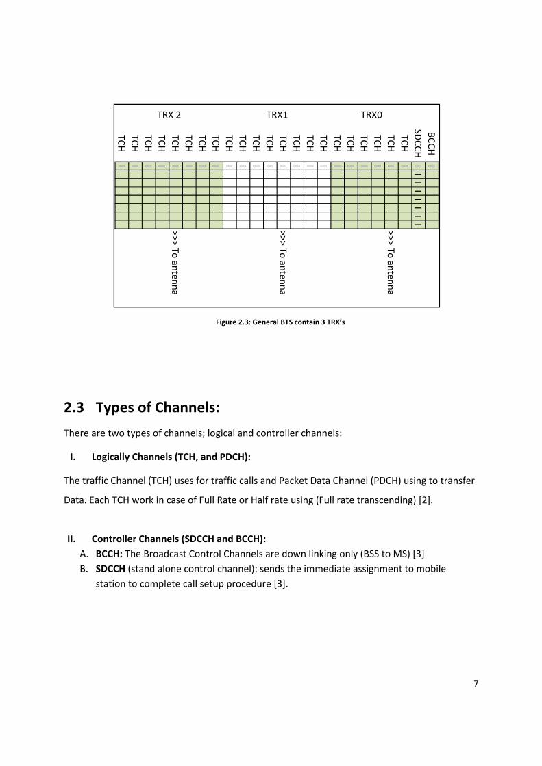
2.2.2 BTS Architecture: Each BTS contains from TRX’s called (Radio), each Radio has single frequency. By using TDMA
technology we can define 8‐Timeslots in each frequency as shown in Figure 2.2.
Time division
fo Frequency Spectrum
Figure 2.2: TDMA technology
The arrangement of Radios in BTS is shows in Figure 2.3. The TRX number 0 has Broadcasting
controller channel (BCCH) and stand alone controller channel (SDCCH) controller channels. This
means that 6‐users can be using TRX0 at the same time. SDCCH is called SDCCH/8 since it has 8
Time slots to work as immediate assignment.
7
2.3 Types of Channels:
There are two types of channels; logical and controller channels:
I. Logically Channels (TCH, and PDCH):
The traffic Channel (TCH) uses for traffic calls and Packet Data Channel (PDCH) using to transfer
Data. Each TCH work in case of Full Rate or Half rate using (Full rate transcending) [2].
II. Controller Channels (SDCCH and BCCH): A. BCCH: The Broadcast Control Channels are down linking only (BSS to MS) [3] B. SDCCH (stand alone control channel): sends the immediate assignment to mobile
station to complete call setup procedure [3].
Figure 2.3: General BTS contain 3 TRX’s
BCCHI
SDCCH
IIIIIIII
TCHI
TCHI
>>> To antennaTCH
ITCH
ITCH
ITCH
ITCH
ITCH
ITCH
ITCH
I>>> To antenna
TCHI
TCHI
TCHI
TCHI
TCHI
TCHI
TCHI
TCHI
>>> To antennaTCH
ITCH
ITCH
ITCH
I
TRX0TRX1TRX 2

8
2.4 Power Level Transmitted and Sensitivity:
The power transmitted from antenna in tower is ‐47dBm as downlink signal. Minimum power
required from mobile to connect with its BTS is ‐110dBm, and it’s different from mobile to
mobile due to the different sensitivity of different mobiles antennas.
2.5 Frequency Bands
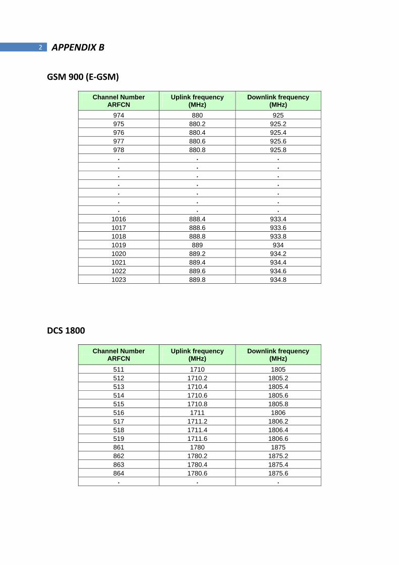
Table 2.1 contains the frequency bands for GSM and DCS systems. To avoid the fractions in
frequency; the companies of mobile communication uses the abbreviation absolute radio
frequency channel number (ARFCN) to define the uplink and downlink frequency at the same
time, (see Appendix B).
Table 2.1: GSM systems Frequencies
GSM system Uplink frequency band downlink frequency band
GSM 900 890 ‐ 915 MHz 935 ‐ 960 MHz
GSM 900 Extended Band 880 ‐ 915 MHz 925 ‐ 960 MHz
DCS 18002 1710 ‐ 1785 MHz 1805 ‐ 1880 MHz
2.6 Frequency Hopping System:
Before explaining this technology you must know that the mobile changes its tuned frequency
for the following reasons:
1. Due to Level of power transmitting, so its search about frequency has maximum power.
2. Due to interferences, so its search about frequency has minimum interference.
2 DCS1800 digital cellular network at 1800 MHz

9
The frequency hopping in simple word is a technology of changing tuned frequency of traffic
channel due to mobile phone periodically (in each 0.5 Sec).
The frequency means: that only TRX’s has only TCH, so the TRX’s have BCCH is not including in
Frequency Hopping system [4].
10
Chapter
3 JAMMING TECHNIQUES
After the background information of GSM/DCS systems, it does make sense to have
information about the methods which followed to jam the communication systems. In
general, the Jamming is successful when the jamming signal denies the communication
Process. This chapter will describe these methods (jamming techniques) in details that based
on two basic ideas: noise mixing and phase changing to obstruct and block the original signal.
3.1 Jamming Strategies:
3.1.1 Noise Strategies:
The main idea here is to insert additional noise in receivers which prevent these Rx from
getting the correct information from the receiving signal. Almost all the techniques which
will be discussed later depend on these strategies [5].
3.1.2 Phase Strategies:
The main idea is to change the phase of signals to prevent the receivers which uses this
phase to receive signal in correct phase.
3.2 Jamming Techniques
3.2.1 Noise Jamming:
The carrier signal is modulated with noise to insert noise into the receiver. By this the
jammer can emit multiple tones, usually; the placement of these tones is based on some
knowledge of the target or targets to be jammed. Noise is used to raise the background

11
noise in the spectrum in which the target system is operating. The bandwidth of the signal
can be as wide as the entire spectrum width used by the target system or much narrower,
occupying only a single channel. These choose makes these kinds of noise jamming [5].
3.2.1.1 Broadband Noise (BBN) Jamming:
Broadband noise (BBN) jamming places noise energy across the entire width of the
frequency spectrum used by the target system radios. It is also called full band or barrage
jamming. This type of jamming is useful against all forms of target system communications. It
is generally useful for coverage an area for screening purposes as well [5].
The limitation of this jamming that is result in low jo (jamming signal power) and this low
power is spread very wide. The BBN can effect on synchronization as Fast Frequency
Hopping (FHSS) which typically need resynchronize on every transmission attempt [5].
The synchronization consists of aligning the time epoch of the transmitter at the receiver and
aligning the PN code sequence. The later causes the receiver to hop to the same frequencies
as the transmitter, while the former insures that these hops occur at the same time. If the
receiver is precluded from synchronization with the transmitter then communication is
denied. The BBN jamming raises the background noise levels and can be used to attack the
synchronization process. Possible BBN jamming spectrum is shown in Figure 3.1 (b)
3.2.1.2 Partial‐Band Noise (PBN) Jamming:
PBN jamming places noise‐jamming energy across multiple, but not all channels in the
spectrum used by the targets [5]. These channels may or not may be contiguous. Possible
PBN jamming spectrum is shown in Figure 3.1 (C, d)

12
3.2.1.3 Narrowband Noise (NBN) Jamming:
NBN jamming places all the jamming energy in a single channel. The bandwidth of this
energy injection could be the whole width of the channel or it could be only the data signal
width or the complementary signal width [5].
Possible NBN jamming spectrum in Figure 3.1 (e)
3.2.2 Tone Jamming:
In tone jamming, one or more jammer tones are strategically placed in the spectrum. Where
they are placed and their number affects the jamming performance. There is two type of
tone jamming [5]:
A. Single tone jamming where signal tunes are placed where it’s needed.
B. Multi tone jamming distributes the jammer power among several tones.
The phase of the jammer tone relative to the target signal can be important parameter,
when there is a single tone jamming signal its well be either at the mark or space frequency.
If it's at the mark frequency, then the phase can present a problem when the jammer tone is
sufficiently out of phase with the symbol signal. If it's at the space frequency, then if the JSR
is large enough the symbol is jammed independent of the phase relationship [5].
It’s still need to mention that the single tone is suitable for direct sequence spread spectrum
(DSS), but not for the changing frequency system like FHSS, however the multi tone jamming
can deal with the FHSS. Possible single‐tone jamming spectrum is shown in Figure 3.1 (f) and
g‐MT in (g).
3.2.3 Swept Jamming:
In swept jamming a relatively narrowband signal which could be as narrow tone but more
often PBN signal, is swept or scanned in time across the frequency band of interest. At any
instant in time, the jammer is centered on a narrow region around this frequency. However,
since the signal is swept, abroad range of frequencies can be jammed in a short period.
When implemented digitally, for example, the jammer may spend 100µs at any one
frequency before moving on to the next band to be jammed. Normally these bands would be

13
consecutive but have not to be, the bands could actually be selected randomally with digital
synthesizer generating the jamming waveform. In this way, this jammer could cover the
whole 30 to 90 MHZ band in about 240 ms; here the full power of the jammer is employed at
each dwell bandwidth. It's possible to avoid certain bands that might be in use by friendly
forces. This is true only when the timing is tailored to the target receiver so that the jamming
signal is present at the receiver for an adequate dwell time. By sweeping the jamming wave
form over a whole range of spectrum, then the jammer is ensure to jam at the entire set of
hop frequencies. Timing is important here, the sweeping must be fast enough to that the
whole band is covered in a sufficiently short period or hops will occur for which no jamming
signal is present. For example to cover the 60 MHZ in the low VHF range 10 times per second
requires a sweep rate of 600 MHZ per second [5].
3.2.4 Pulse Jamming:
This technique is similar in concept to partial band noise jamming. Pulse jamming can have
lower average power than some of other jamming techniques discussed here, and be just as
more effective. The duty cycle determines the relationship between the average power and
peak power. The jamming effects depend on the peak power and how often that signal
returns to the receiver [5].
3.2.5 Follower Jamming:
This Jammer attempts to locate the frequency to which the frequency hopping transmitter is
sent, to identify the signal as the one of interest (the target), and jam at the new frequency.
This jamming waveform could be in the form of tones or it could modulate the tones with,
say, noise using FM modulation. Follower jamming is also referred to as responsive jamming,
repeater jamming, and repeater back jamming [5].

14
Figure 3.1: a‐channelized spectrum, b‐full band jamming, c‐ contiguous partial band jammingd‐ Non d contiguous partial band jamming, e – narrowband noise jamming, f –single tone
jamming, and g‐MT jamming
Amplitude
(a)
Amplitude
(b)
Amplitude
(c)
Amplitude
(d)
Amplitude
(e)
Amplitude
(f)
Amplitude
(g)
Frequency
Frequency
Frequency
Frequency
Frequency
Frequency
Frequency

15
3.2.6 Smart Jamming
This category of jamming techniques attempts to disrupt portions of digital signals only,
selecting only those portions necessary to deny communications, if possible.
To describe the system in a block diagram shown in Figure 3.2, let's discuss two cases: First
case, the GSM Scanner and Power detector Systems detects a mobile phone in the restricted
area and gives information to computer about the frequency used by mobile phone, and
then the computer gives the circuit interface system an instruction to prepare the jamming
system to block the mobile phone. Second case, when the GSM scanner and power detector
systems are not detecting mobile phone in the restricted area for a time specified in
computer, the computer gives the circuit interface an instruction to shift the jamming system
into standby mode.
Figure 3.2: General block diagram for intelligent jamming system

16
Chapter
4 METHODOLOGY AND ELECTRONIC CIRCUITS IMPLEMENTATION
The deep view inside the system will show each stage and the circuits in details. This chapter
will talk about the Methodology to build the jamming system from the electronic point of
view and it will explain clearly the main function of each single circuit and its theoretical
information also this chapter contains analysis and design for each circuit by using the
advance design system software package such as mixer, noise generator….etc.
4.1 Methodology
To build this project; the system must be divided into two phases; the first phase as the
jamming system and the second one is to control the jamming system to be an intelligent
jamming system. These subsystems and stages are coming from different functions of each
small component, so let’s discuss the purpose of each stage by explaining the operation of
the system.
The main purpose of the overall system is to disable or block mobile phones in the restricted
area. As shown in Figure 4.1 the intelligent jamming system is designed to work as detector,
where the Mobile detector are detect the RF signals from mobile and supply the PIC
microcontroller by the required information to check if there is mobile phone around or not.
The synthesizer then will be enabled by PIC to block the desired frequency. The desired
frequency here means the controller channel that can be detected using TEMS pocket that
will be explained later in chapter six.

17
The jamming system will produce the jamming signal by mixing the noise with intermediate
frequency and then modulate into UHF (Ultra High Frequency) range for mobile
communication system as single side band (SSB). The switching system will choose the mobile
communication system to jam (GSM or DCS). Finally the signal must be amplified to be
propagated.
The design of any stage of the system is depends on the characteristics of the problem. In this
design of the project is supported by the Agilent technology software package called ADS and
other tools using to program the intelligent controller such as PIC microcontroller.
Figure 4.1: Mobile phone intelligent jamming system block diagram

18
This project can be implemented in two phases; the first one is the Design and Simulation by
Using ADS. As shown in Figure 4.1 the jamming system is characterized by the intermediate
frequency (IF) stage, radio frequency (RF) stage, and Transmission stage. Also signal
processing in order to select control Channels is done by TEMS pocket software.
The UHF modulation, in order to modulate the signal to be transmitted is shown in Figure 4.1
as IQ modulator. Finally the transmission stage is required to propagate the signal through
antenna.
4.2 Mobile Detector
Proceeding from the intelligently of the project it is important to find or design a circuit that
can detect calling process and give a warning to the control system to shift the jamming into
power on mode. This section has a brief description about the calling detector circuit, its
components and the testing results.
This circuit3 is shown in Figure 4.2 can sense the presence of an activated mobile phone from
a distance of one and half (1.5) meter. It can detect the incoming and outgoing calls, SMS and
video transmission even if the mobile phone is kept in the silent mode. At the moment the
bug detects RF transmission signal from an activated mobile phone, it starts sounding a beep
alarm and the LED blinks. The alarm continues until the signal transmission ceases.
The circuit as shown in Figure 4.2 consists of four main stages
1. Capturing RF transmission stage.
2. Current to voltage converter
3. Trigger stage
4. Timer stage
3 D. MOHAN KUMAR, “Mobile Bug”, Electronics for you magazine, 2008
19
Capturing RF transmission stage
This stage can capture all frequencies in the mobile communication spectrum from 0.9 to 3 GHz
with a wavelength of 3.3 to 10 cm. To do the detection job this stage uses a 0.22μF disk
capacitor (C3), this capacitor stores energy and transfers the stored energy in the form of
minute current to the inputs of the stage of current to voltage converting.
Current to Voltage converter Stage
The aim of this stage is to convert the minute current from the previous stage into the
corresponding output voltage by using a current to voltage convertor (CA3130).
Trigger stage
This stage used to trigger the timer stage and provide an Invisible alert about the transmission
mobile data occurrence this trigger used a monostable timer (NE555).
Figure 4.2: Mobile detector

20
4.3 IF Stage 4.3.1 Triangular Wave Generator:
Figure 4.3 shows the triangular wave generator circuit [6], it is containing two stages the first
is the Schmitt trigger that generates square wave and the other is the integrator circuit that
integrate the square wave to the triangle wave. The triangular wave oscillator is composed of
the Schmitt circuit and the integration circuit.
(The value of frequency generated from this circuit depends on the ratio of the resistors R2
and R3).
In this project the period of Triangle wave required to block GSM system is defined as
following:
T = .577 msec × 2 =1.154 msec
Where: .577msec is the time of each time slot.
Figure 4.3: Triangle wave Generator

21
Figure 4.4: Square wave from Point A
Figure 4.5: Triangular wave from Point B
Figure 4.6: Practical Triangle Signal

22
4.3.2 Noise Generator:
In this project the jamming system needs a certain type of noise to cover a portion band of
spectrum, so the most applicable type of noise in this case is the white noise. The noise in
general can be defined as a Random movement of charges or charge carriers in an electronic
device generates current and voltage that vary randomly with time [7].
4.3.2.1 White Noise
White noise is a random signal (or process) with a flat power spectral density. In other words,
the signal's power spectral density has equal power in any band, at any centre frequency,
having a given bandwidth. White noise is considered analogous to white light which contains
all frequencies [7]. An infinite‐bandwidth, white noise signal is purely a theoretical
construction. By having power at all frequencies, the total power of such a signal is infinite. In
practice, a signal can be "white" with a flat spectrum over a defined frequency band [7].
The requirements are to find a circuit which generates a white noise. The circuit as shown in
Figure 4.7 will generate the noise required for the jamming system.
Figure 4.7: Noise Oscillator

23
4.3.2.2 Amplifier Stage
To amplify the noise generated by the previous circuit; the two stages of amplification in Figure 5.7 is used.
The capacitor C4 is just for blocking DC. The value of the resistor forms the none‐inverting Amplifier and its gain is given by (1+ R/R2). The noise waveform is shown in Figure 4.9 and 4.10.
Figure 4.9: Output Noise waveform
Figure 4.8: Amplifier Stages to Amplify the Noise

24
4.3.3 Mixer:
Mixer is a nonlinear circuit that combines two signals in such away to produce the sum and
difference of the two input frequencies at the output [8].
4.3.3.1 Transistor Mixer:
In this project the mixer uses FET transistor; scince it’s a low noise device and fast in
response, so its efficient device in this case. The FET Circuit illustrates the technique of
summing the two input signal at a single input terminal (both IN1 and IN2 are applied to the
gate) [8]. FETs can be used in mixers in both active and passive modes.
There are different types of mixers and different techniques; in this project the mixer uses the
simple summer circuit contains from just one dual OPAMP (TL082) as shown Figure 4.12 [6].
TL082 OP‐AMP as shown in Figure 4.11 is a high speed J–FET input dual operational amplifiers
incorporating well matched, high voltage J–FET and bipolar transistors in a monolithic
integrated circuit. The devices feature high slew rates, low input bias and offset current, and
low offset voltage temperature coefficient.
Figure 4.10: Practical Output Noise

25
Figure 4.13: Practical Mixed waveform
Figure 4.12: OPAMP Mixer
Figure 4.11: TL082 J‐FET OPAMP

26
4.3.4 Voltage Control Oscillator:
In this project the voltage control oscillator is used to generate a portion of modulated signal
from 2 kHz ‐ 310 kHz, bandwidth 200 kHz as the GSM mobile communication channel
bandwidth.
4.3.4.1 Oscillator Performance Parameter:
Frequency tuning range is one of the most fundamental tradeoffs in an oscillator. The Q
factor of the resonator sets the noise performance of the oscillator. In general, the more
tunable an oscillator is the lower the Q of the resonator [9].
Any amplifier can be made to oscillate if a portion of the output is fed back to the input in
such away the (Barkhausen Criteria) Figure 4.14 shows the basic block diagram to any
oscillator [8]. The two conditions must be satisfied to be oscillator to oscillate [8]:
A. AB = 1
B. 2
A
B
Figure 4.14: Basic Oscillator

27
The MAX038 as shown in Figure 4.15 is a high‐frequency, precision function generator
producing accurate, high‐frequency triangle, sawtooth, sine, square, and pulse waveforms
with a minimum of external components. The output frequency can be controlled over a
frequency range of 0.1Hz to 20MHz.
The output of the mixer in entered to MAX038 from IN pin within series Resistor to convert
the voltage into current. CF changed to 1 nF also the output is sin wave so Ao = logic 1 and A1
= logic 1.
Figure 4.15: MAX038 function generator

28
The voltage controlled oscillator configuration is shown in Figure 4.16 [10].
Figure 4.16: MAX038 Voltage controlled oscillator
Figure 4.17: Transient simulation for Voltage controlled oscillator output

29
4.4 RF Stage 4.4.1 Synthesizer
It’s a device which is used as a tunable oscillator. The ADF4156 is shown in Figure 4.19 and
4.20 is a 6 GHz fractional‐N frequency synthesizer that implements local oscillators in the up
and down conversions sections of wireless receivers and transmitters.
Figure 4.19: (AD4156) Sigma‐Delta Fractional‐N Synthesizer
Figure 4.18: Practical VCO output waveform

30
Figure 4.20: ADF4157 Frequency Synthesizer
The following equation governs how the synthesizer should be programmed [11]:
RFOUT NFRAC225 FPFD
Where:
RFOUT is the RF frequency output.
N is the integer division factor.
FRAC is the fractionality.
This IC has Evaluation kit to configure the interfacing with the computer and to provide the
synthesizer the Reference frequency as shown in Figure 4.21 [11].

31
4.4.2 RF Mixer
As mentioned before; the jamming signal must have the same frequency of the controller
channel with bandwidth equal to (200KHz) provided from VCO in the IF stage, so you need to
carry this baseband on a suitable carrier which have the frequency of controller channel; to
do this its useful to use the RF Mixer as shown in figure 4.22.
Figure 4.21: EVAL KIT for Synthesizer
Figure 4.22: RF Mixer
32
RF Mixer is shown in Figure 4.22 [12] is used to produce a modulated signal mixed with noise.
The carrier frequency will be fed to the modulator by the synthesizer, and the baseband from
the VCO in IF stage. The introducing of Double sideband (DSB) signal can be done by feeding
the IF signal from I terminal and carrier from LO terminal [13].
4.4.3 Power Splitter
After the signal mixed with carrier frequency and become in UHF range, the second step is to
amplify the signal to be transmitted. The transmission stage has two branches; 900 MHz
branch and 1800 MHz branch, so to divide the common signal between two branches; the
splitting process will be used.
4.4.3.1 Power Splitter:
Splitters are used extensively in wireless signal distribution networks, to split the base station
transmitted signal, Tx, into many different paths to reach multiple antennas, and at the same
time to transmit the signals received by the antennas, Rx, back to the base station receiver
[14].
Figure 4.23: Wilkinson Power Splitter

33
Wilkinson Splitters is shown in Figure 4.23 for microwave frequencies generally use a
microstrip design. They consist of a pair of quarter wave (λ/4) transmission line sections with
characteristic impedance of 70.7Ω which are series terminated at the output with a 100Ω
resistor [14].
The design of power splitter using AutoCAD is shown in Figure 4.24.
Figure 4.24: Power Splitter design

34
In this project because of problems to build the RF circuits PCB’s we use the RF Power Splitter
module as shown in figure 4.25.
4.4.4 Power Amplifier
First let’s calculate the minimum power required to block the GSM‐900 and DCS (Jr):
For GSM‐900 the minimum signal to noise ratio (SNR min=9 dB) and maximum signal power (S
MAX =‐15dBm) [16].
Now , so Jr (dB) =‐15 ‐ 9=‐24dBm. To cover area of 20 meter radius; the free
space power loss (FSPL) should be calculated as follow:
FSPL=20log [17].
Where:
R and in meter
For 960MHz 0.3125 m, substituting in FSPL equation gives:
FSPL= 58 dB, then Jr=‐24 + 58 = 34dBm.
For DCS:
SNR min=9 dB and S MAX = ‐23dBm [16].
Repeating the calculation with f = 1880 gives:
Jr = ‐32 + 63.9 = 31.9dBm.
To meet this power we need a power amplifier.
Figure 4.25: RF Power Splitter

35
4.4.4.1 Power Amplifier DCS‐1800
It’s a power amplifier which can be used to give the sufficient power for jamming signal in
range of DCS downlink frequency (1805 ‐ 1880 MHz). This power amplifier can give 33dBm
maximum power. The Figure 4.26 shows the power amplifier module from RFbayinc [18].
But the power coming from synthesizer is not sufficient to be amplified to 33dBm as shown in
figure 4.27 to get 33dBm output; the input power must be from (10‐15)dBm; so the RF
Amplifier MRA‐2000 is used to amplify the input signal from 0 to 10dBm.
Figure 4.26: MPA 19‐20 Power Amplifier
Figure 4.27: Output Power with respect to Input Power

36
4.4.4.2 Power Amplifier GSM‐900
This power amplifier is suitable for GSM‐900 downlink frequency (925‐960MHz). This power
amplifier can give 34dBm maximum power. The Figure 4.28 shows the power amplifier
module from RFbayinc [19]. In this power amplifier there is no need to amplify the signal fed
from synthesizer because it is sufficient to get the desired output power.
4.4.5 Antenna
The final stage in any Transmitter communication system is the Antenna, in this project of
intelligent jamming system for GSM, needs to antenna works in frequency of GSM and DCS
systems as explained in chapter 2. The antenna has shown in Figure 4.30 support multiple
mobile systems like [AMPS, GSM, DCS, PCS and UMTS]. The radiation pattern of this antenna
is omni with vertical polarization also has 2dBi gain [20].
Figure 4.29: Antenna
Figure 4.28: MPA‐0925 Power Amplifier

37
4.4.6 PCB Boards Layouts
By using PCB (Printed circuit board) program to draw the layout of the circuit in this project
like [IF stage, Power Amplifiers for 900 and 1800, Power splitter, Mobile detector ver.1 and
ver.2] as follow:
Figure 4.30: IF Stage PCB

38
Figure 4.31: Mobile detector Ver.1
Figure 4.32: Mobile detector Ver.2

39
4.4.7 Power Supply
The main operator of the jamming system from the electricity point of view is the electrical
power because it will bias and feed each stage in the system. This section will explain the
relationship between the power supply and other stages in the system.
In general the power supply consists of transformation, rectification. Filtration and regulation
as shown in the Figure 4.36 [6]:
The Figure 4.36 shows the general power supply circuit that can be explained each of them as follow:
1. The transformer is used to step down the input voltage from 220 to the desired values.
2. The rectifier stage is used to convert the signal from AC to DC.
3. Filter is used to reduce the ripple of voltage that results from rectifier stage.
4. The regulator is used for safety and to ensure a fixed voltage across a certain load in the
circuits in case the input values or the load are changed so it have the concept of the
zener diode principle. As example on the regulators L200 IC with high voltage.
Power supply
Transformer Rectifier FilterInput voltage
To VCO
To Oscillator
To noise circuit
Regulator
Figure 4.33: Block diagram to power supply
40
4.4.7.1 The Operation of Power Supply
There are two ways to supply the system with required voltages:
1. Using AC to DC power supply, which gives directly the wanted values, for example the
power supply of the PC which has a complex arrangement of electrical components,
including diodes, capacitors and transformers, this special power supply is called switched
mode power supply (SMPS), the switching process is to convert the current frequency
from 50 Hz to higher frequency; to reduce the ripple that inversely proportional to
frequency. Their outputs are: 3.3, 5, 9, 12 and ‐5, ‐9, ‐12. This method is not used in this
project because the system needs to 28 V.
2. Building a power supply from transformer, bridge rectifier, and regulators. In this method
the center tap transformer step down from 220 to 30 is used, then connects a bridge
rectifier like KBPC3510 with two capacitors to get DC signal.
4.4.7.2 Power Supply PCB layout

41
Chapter
5 TEMS POCKET AND PC SOFTWARE
5.1 TEMS Pocket
In this project as intelligent mobile jamming, the most important feature of this system is
simplified in simple worlds as how to know the controller channel frequency in the neighbor
base stations to block it only. The manually method to measure the frequency of the
controller channel which needs more than one heavy equipments like spectrum analyzer and
antenna adapter also need someone has experience in mobile communication specially in
GSM system, so the TEMS Pocket is an optimum solution to this case.
TEMS Pocket is a basic mobile network diagnostics tool built into an Ericsson T610 GPRS
mobile station. TEMS Pocket is suitable for day‐to‐day verification, maintenance and
troubleshooting of mobile networks but is also handy for many cell planning tasks [21].
The interface of TEMS pocket have a number of parameters not all these parameters is
important in this project see Figure 5.1.
Figure 5.1: TEMS pocket interface
42
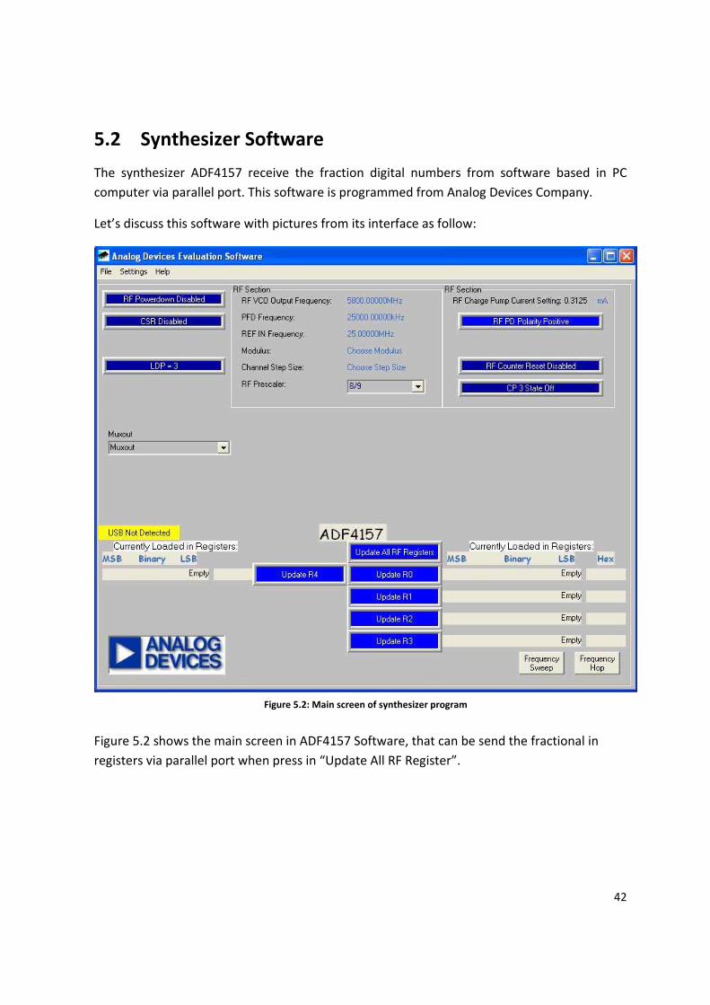
5.2 Synthesizer Software
The synthesizer ADF4157 receive the fraction digital numbers from software based in PC computer via parallel port. This software is programmed from Analog Devices Company.
Let’s discuss this software with pictures from its interface as follow:
Figure 5.2 shows the main screen in ADF4157 Software, that can be send the fractional in registers via parallel port when press in “Update All RF Register”.
Figure 5.2: Main screen of synthesizer program

43
As shown in Figure 5.3 the output frequency in VCO can be changed and then press the
“Update R0 and R1” button, other feature can be changed like step size and ref. division.
Figure 5.3: RF output frequency screen

44
Chapter
6 PIC MICROCONTROLLER AND COMPUTER PORTS
The intelligent system needs to be under control and to have a specific output according to a
specific input. One of the most important digital controllers is the PIC microcontroller that
stands for “Programmable Interface Controller”. This chapter will talk about the PIC types and
the related assembly codes. Also it will determine which one to be used in this project.
6.1 The PIC Microcontroller
PIC is a family of microcontrollers made by Microchip Technology. The original one was the
PIC1650 developed by General Instruments. This device was called PIC for “Programmable
Intelligent Computer” although it is now associated with “Programmable Interface Controller”
Instead they prefer the brand name PICMicro. Popular wisdom relates that PIC is a registered
brand in Germany and Microchip is unable to use it internationally [22].
6.1.1 PIC Families:
There are three families of PICMicro:
1. Baseline PIC Family
2. Mid‐range PIC Family
3. High‐Performance PIC Family

45
6.1.2 PIC Pin Mapping:
Figure 6.1 is a topview of the PIC IC chip, also the name and function of each pin is tabulated in
Table 6.1.
Table 6.1: PIC Pin Mapping
Pin Number Pin Name Function 1 Port A Bidirectional pin I/O 2 Port A Bidirectional pin I/O
3 Port A Bidirectional pin I/O, TOCK1 which functions as a timer
4 MCLR Reset System (0 to active)5 VSS 0 Volt (GND) 6 Port B Bidirectional pin I/O, Interrupt input 7 Port B Bidirectional pin I/O 8 Port B Bidirectional pin I/O 9 Port B Bidirectional pin I/O 10 Port B Bidirectional pin I/O 11 Port B Bidirectional pin I/O 12 Port B Bidirectional pin I/O 13 Port B Bidirectional pin I/O 14 VDD +5 Volt (biasing) 15 OSC2 Crystal Terminal (Oscillator) 16 OSC1 Crystal Terminal (Oscillator) 17 Port A Bidirectional pin I/O 18 Port A Bidirectional pin I/O
6.1.3 Synthesizer‐Mobile Detector Controlling System
PIC microcontroller can be programmed using Assembly or C language. In this project the program is using C language because it’s easy to understand and implement, (see Appendix C) that contains the PIC program instruction set. In Figure 6.3 shows the flow chart of PIC microcontroller to control the Mobile detector cyclic check sensing.
This program performed to check the logic level coming from mobile detector. If the logic level
input to PIC terminals is high the PIC will give a low logic level to enable the synthesizer and vice
versa. The calling detector provides trigger that indicates about there is a mobile phone in the
restricted area or not as shown in Figure 6.2.
Figure 6.1: PIC Micro Controller

46
The Schmitt trigger converts the level of pluses into suitable level to PIC, and then the PIC will
decide the output logic as following state in Table 6.1:
Table 6.2: PIC Logic state
INPUT OUTPUT EN’ 1 0 0 1
The PIC microcontroller still provides EN’ logic (0) after he gets a logic (1) from the calling
detector for a short time specified in the PIC code; in this case the program adjusted to provide
the EN’ logic for 20msec. then the PIC automatically gives a logic (1) to disable the jamming and
shift the system into standby mode see flowchart in Figure 6.3.
Figure 6.2: Standby controlling block diagram

47
Figure 6.3: PIC flow chart program
48
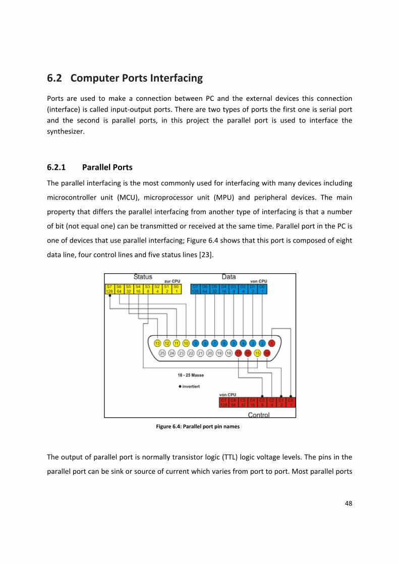
6.2 Computer Ports Interfacing
Ports are used to make a connection between PC and the external devices this connection (interface) is called input‐output ports. There are two types of ports the first one is serial port and the second is parallel ports, in this project the parallel port is used to interface the synthesizer.
6.2.1 Parallel Ports
The parallel interfacing is the most commonly used for interfacing with many devices including
microcontroller unit (MCU), microprocessor unit (MPU) and peripheral devices. The main
property that differs the parallel interfacing from another type of interfacing is that a number
of bit (not equal one) can be transmitted or received at the same time. Parallel port in the PC is
one of devices that use parallel interfacing; Figure 6.4 shows that this port is composed of eight
data line, four control lines and five status lines [23].
The output of parallel port is normally transistor logic (TTL) logic voltage levels. The pins in the
parallel port can be sink or source of current which varies from port to port. Most parallel ports
Figure 6.4: Parallel port pin names

49
implemented in ASIC, can sink and source around 12mA, Sink/Source 6mA, Source 12mA/Sink
20mA, Sink 16mA/Source 4mA, and Sink/Source 12mA.

50
Chapter
7 CONCLUSIONS AND FUTURE RECOMMENDATIONS
7.1 Conclusions
This project is designed to be an intelligent jamming system for GSM‐900 and DCS‐1800
systems with an ability to be controlled by computer and to have a standby mode.
The main stages in the system are completed successfully; such as the IF stage, and the RF
stage components are imported and it will be implemented on printed circuit board (PCB) in
the earlier future.
The main problems were in RF stage, because the dealing with the high frequency signal
needs special components such as surface mount (SMD) capacitors and resisters, also the PCB
needs microstrip lines, so the problems appear in matching the stages with each other; where
sometimes a power attenuator between two stages was needed.
The coverage area of the calling detector was not sufficient; so an in improvement must be
done to give the needed coverage.
There is a problem appears in determining the controller channel that may be changes due to
power level, so the system must be configured to block the controller channel with its
neighbors.

51
This signal must have an essential level of power equal to 34dBm to satisfy the jamming
condition.
7.2 Future Recommendations
Until this point the present work suffered from the carrier system “Synthesizer”, there is no a
ready evaluation Kit provide frequency from 900‐1900 MHz. in future to improve and develop
this project it is recommended to explore the following ideas:
1. Study and learn the fabrication procedures of the RF PCB circuit or find an alternative
method to build frequency synthesizer. In addition find the required equipments to
build the RF PCB’s.
2. Design and implement a microprocessor system to control the frequency synthesizer
directly without the PC.
3. Rebuild and arrange the system package in such a way to minimize the overall system
size.
4. Improve the calling detector range to detect the mobiles in wider area.
5. Research about the ability to jam specific calls and allows other important calls like
emergency numbers to pass.

I
References [1]: LAWRENCE HARTE AND DAVID BOWLER, “Introduction To Mobile Telephone Systems
Wireless Technologies And Services”, 2004.
[2]: MOTOROLA, Introduction to digital cellular, for training professional only. 2001
[3]: HUAWEI Co., “UMNIAH Company Manuals”.
[4]: ERICSSON, “open information user descriptions about frequency hopping”.
[5]: RICHARD A.POISEL, “Modern Communications Jamming Principles and Techniques”,
ARTECH House, 2004.
[6]: DONALD A. NEAMEN, “Electronic Circuit Analysis and Design”, john Willey, 2nd edition.
[7]: Devendra K.Misra, “Radio frequency and Microwave communication Circuit Analysis and
Design”.
[8]: Joseph J. Carr, “Secrets of RF Circuit Design”, 2nd edition
[9]: JASON BREITBARTH B.S. Electrical Engineering, “OCTAVE TUNING, HIGH FREQUENCY
VARACTOR OSCILLATOR DESIGN”,Oregon State University, 1997.
[10]: MAXIM 038, “High‐Frequency Waveform Generator data sheet”, 2007
[11]: Analog devices ADF4157,”6 GHz Fractional‐N Frequency Synthesizer data sheet”, 2006
[12]: Rfbayinc Products, “MXR‐20 RF Mixer”
[13]: B.P.Lathi, “Modern digital and analog communication Systems”, 3rd edition
[14]: MICROLAB/FXR, “choosing splitter”, A Wireless Telecom Group Company
[15]: NEC devices PG2214TB, “GaAs INTEGRATED CIRCUIT SPDT Switch”
[16]: Horst Fischer, Frank Henkel, Michael Engels, Peter Waldow,” UMTS/GSM MULTI MODE
RECEIVER DESIGN”, IMST GmbH, Carl‐Friedrich‐Gauss‐Str. 2, 47475 Kamp‐Lintfort,
Germany
[17]: Glover and Grant, “Digital Communications”, 2nd edition
[18]: Rfbayinc Products, “MPA‐19‐20 Power Amplifier”
[19]: Rfbayinc Products, “MPA‐0925 Power Amplifier”

II
[20]: Nearson Antennas, “Multiple Band Swivel Antenna”, 2007
[21]: Ericson TEMS, “TEMS Pocket GSM T68i user manual”, 2003
[22]: A. Salhot, Abdallah, “PICMicro MCU microcontroller Programming”, 2006 Amman
[23]: Dhananjay, “Programming the Parallel Port”, 1998

1 APPENDIX A
Lists of GSM abbreviations
A
ARFCN Absolute Radio Frequency Channel Number: An integer which defines the absolute RF
channel number
AUC Authentication Centre: A GSM network entity which provides the functionality for verifying the
identity of an MS when requested by the system often a part of the HLR.
B
BC broadcast control
BCCH broadcast control channel
BS base station
BSC base station controller
BSS base station system
BTS base transceiver station
C
CA Cell Allocation: The radio frequency channels allocated to a particular cell
D
DCS1800 digital cellular network at 1800 MHz
E
EIR equipment identity register
EGSM900 Extended GSM900
F
FDMA frequency division multiple access
FH frequency hopping
2 APPENDIX A
G
GPRS general packet radio service
GSM global system for mobile communications
GSM MS GSM mobile station
H
HLR home location register
HR Half rate: Refers to a type of data channel that will double the current GSM air interface capacity
to 16 simultaneous calls per carrier (see also FR – Full Rate).
I
IMSI International Mobile Subscriber Identity Published mobile number (prior to ISDN) (see also
MSISDN) that uniquely identifies the subscription. It can serve as a key to derive subscriber
information such as directory number(s) from the HLR.
L
LR location registration
LAPDm Link Access Protocol on the Dm channel
M
MS mobile station
MSC mobile switching centre
Multiframe Two types of multiframe are defined in the system: a 26-frame multiframe with a period of
120 ms and a 51-frame multiframe with a period of 3060/13 msec
O
OMC Operations and Maintenance Centre the OMC node of the GSM TMN provides dynamic O&M
monitoring and control of the PLMN nodes operating in the geographical area controlled by the
specific OMC.

3 APPENDIX A
P
PIN personal identification number
PSTN public switched telephone network
Pegging modifying a statistical value
R
RACH random access channel
S
SDCCH stand alone control channel
T
TDMA time division multiple access
TA Time Advance
TCH Traffic Channel GSM logical channels which carry either encoded speech or user data
Timeslot the multiplex subdivision in which voice and signaling bits are sent over the air. Each RF
carrier is divided into 8 timeslots
TRX Transceiver
V
VLR visitor location register

1 APPENDIX B
Compare between ARFCN and frequency
GSM 900 (P‐GSM):
Channel Number ARFCN
Uplink frequency (MHz)
Downlink frequency (MHz)
0 890 935 1 890.2 935.2 2 890.4 935.4 3 890.6 935.6 4 890.8 935.8 . . .. . .. . .. . .. . .. . .. . .. . .
75 905 950 76 905.2 950.2 77 905.4 950.4 78 905.6 950.6 79 905.8 950.8
108 911.6 956.6 109 911.8 956.8 110 912 957 111 912.2 957.2 112 912.4 957.4 113 912.6 957.6 114 912.8 957.8 115 913 958 116 913.2 958.2 117 913.4 958.4 118 913.6 958.6 119 913.8 958.8 120 914 959 121 914.2 959.2 122 914.4 959.4 123 914.6 959.6 124 914.8 959.8
2 APPENDIX B
GSM 900 (E‐GSM)
Channel Number ARFCN
Uplink frequency (MHz)
Downlink frequency (MHz)
974 880 925 975 880.2 925.2 976 880.4 925.4 977 880.6 925.6 978 880.8 925.8
. . .
. . .
. . .
. . .
. . .
. . .
. . .1016 888.4 933.4 1017 888.6 933.6 1018 888.8 933.8 1019 889 934 1020 889.2 934.2 1021 889.4 934.4 1022 889.6 934.6 1023 889.8 934.8
DCS 1800
Channel Number ARFCN
Uplink frequency (MHz)
Downlink frequency (MHz)
511 1710 1805 512 1710.2 1805.2 513 1710.4 1805.4 514 1710.6 1805.6 515 1710.8 1805.8 516 1711 1806 517 1711.2 1806.2 518 1711.4 1806.4 519 1711.6 1806.6 861 1780 1875 862 1780.2 1875.2 863 1780.4 1875.4 864 1780.6 1875.6
. . .

3 APPENDIX B
. . .
. . .
. . .
. . .
. . .
. . .
. . .873 1782.4 1877.4 874 1782.6 1877.6 875 1782.8 1877.8 876 1783 1878 877 1783.2 1878.2 878 1783.4 1878.4 879 1783.6 1878.6 880 1783.8 1878.8 881 1784 1879 882 1784.2 1879.2 883 1784.4 1879.4 884 1784.6 1879.6 885 1784.8 1879.8

1 APPENDIX C
PIC16F84 Program written in C language:
//Defines for microcontroller
//PIC Functions
#pragma CLOCK_FREQ 10000000
#define P16F84A
#include <system.h>
#define MX_EE
#define MX_EE_TYPE1
const char MX_EE_SIZE = 64;
//Macro function declarations
//Variable declarations
char FCV_TEST;
char FCV_INT;
char FCV_TEST2;
//Macro implementations
void main()

2 APPENDIX C
{
//PIC Initialisation
//Interrupt initialisation code
option_reg = 0xC0;
TRISB = TRISB | 0x01;
FCV_INT = (PORTB & 0x01 == 0x01);
while( FCV_INT == 1 )
{
TRISA = TRISA | 0x03;
FCV_TEST2 = PORTA & 0x03;
TRISB = TRISB | 0xfe;
FCV_TEST = PORTB & 0xfe;
if( FCV_TEST | FCV_TEST2 == 0 )
{
TRISA = TRISA & 0xfb;
if (1)
PORTA = PORTA & 0xfb | 0x04;
else
PORTA = PORTA & 0xfb;

3 APPENDIX C
}
else
{
TRISA = TRISA & 0xfb;
if (0)
PORTA = PORTA & 0xfb | 0x04;
else
PORTA = PORTA & 0xfb;
delay_ms(15);
TRISA = TRISA & 0xfb;
if (1)
PORTA = PORTA & 0xfb | 0x04;
else
PORTA = PORTA & 0xfb;
}
}
mainendloop: goto mainendloop;
}

1 APPENDIX D
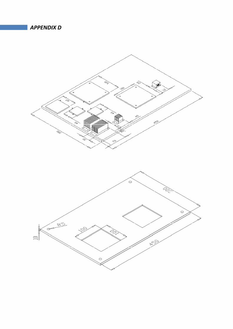
2 APPENDIX D