NEH/L CDP1802 Solid State CDP1802C Division TypesNEH/L SolidState Division Microprocessor Products...
21
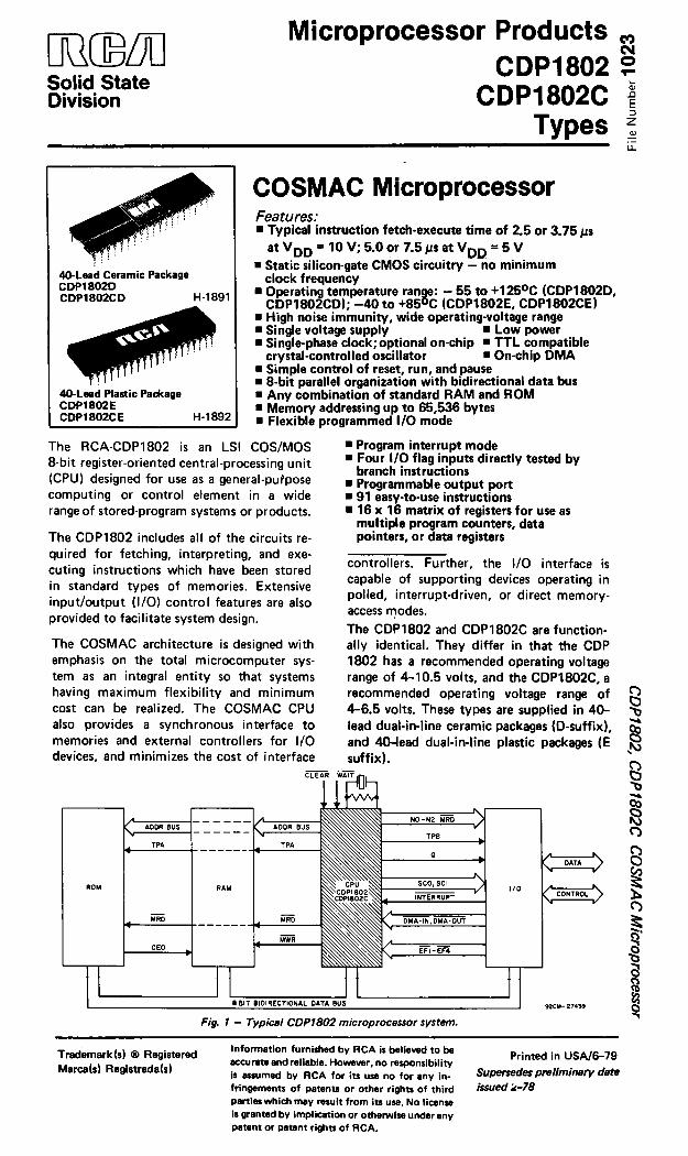
NEH/L Solid State Division Microprocessor Products CDP1802 CDP1802C Types Features: 40-Lead Ceramic Package CDP18020 CDP1802CD H-1891 40-Lead Plastic Package CDP1802E CDP1 BOZCE H-1892 The RCA-CDP1802 is an LSI COS/MOS 8‐bit register-oriented central-processing unit (CPU) designed for use as a general-pufpose computing or control element in a wide range of stored-program systems or products. The CDP1802 includes all of the circuits re quired for fetching, interpreting, and exe‑ cuting instructions which have been stored in standard types of memories. Extensive input/output (l/O) control features are also provided to facilitate system design. The COSMAC architecture is designed with emphasis on the total microcomputer sys‑ tem as an integral entity so that systems having maximum flexibility and minimum cost can be realized. The COSMAC CPU also provides a synchronous interface to memories and external controllers for Ho devices, and minimizes the cost of interface CLEAR WAIT 8 BIT BIDIRECTIONAL DATA BUS COSMAC Microprocessor I Typical instruction fetch-execute time of 2.5 or 3.75 us at VDD =10 V; 5.0 or 7.5 us at VDD =5V I Static silicon-gate CMOS circuitry ‐ no minimum clock frequency I Operating temperature range: - 55 to +125°C (CDP18020, CDP1BOZCD); ‐40 to +85 I High noise immunity, wide operating-voltage range I Single voltage supply I Single-phase clock;optional on-chip I TTL compatible crystal-controlled oscillator I Simple control of reset, run, and pause I 8-bit parallel organization with bidirectional data bus I Any combination of standard RAM and ROM I Memory addressing up to 65,536 bytes I Flexible programmed I/O mode C (CDP1802E, CDP18026E) I Low power I On-chip DMA I Program interrupt mode I Four l/O flag inputs directly tested by branch instructions I Programmable output port I 91 easy-to-use instructions I 16x 16 matrix of registers for use as multiple program counters, data pointers, or data registers controllers. Further, the l/O interface is capable of supporting devices operating in polled, interrupt-driven, or direct memory‑ access rnodes. The CDP1802 and CDP1802C are function‑ ally identical. They differ in that the GDP 1802 has a recommended operating voltage range of 4‐10.5 volts, and the CDP1802C, a recommended operating voltage range of 4-6.5 volts. These types are supplied in 40‑ lead dual-in-line ceramic packages (D-suffix), and 40-Iead dual-in-line plastic packages (E suffix). TPB O 5C0. SCI CONTROL SZCM- 27439 Fig. 1‐ Typical CDP1802 microprocessor system. Trademarkls) ® Registered Mercels) Registredals) Information furnished by RCA is believed to be accurate and reliable. However, no responsibility is assumed by RCA for its use no for any in‑ fringements of patents or other rights of third Printed in USA/6‐79 Supersedes preliminary date issued 2-78 parties which may result from its use. No license is granted by implicationor otherwise under any patentor patent rights of RCA.
Transcript of NEH/L CDP1802 Solid State CDP1802C Division TypesNEH/L SolidState Division Microprocessor Products...
NEH/LSolid StateDivision
Microprocessor ProductsCDP1802
CDP1802CTypes
Features:
40-Lead Ceramic PackageCDP18020CDP1802CD H-1891
40-Lead Plastic PackageCDP1802ECDP1BOZCE H-1892
The RCA-CDP1802 is an LSI COS/MOS8‐bit register-oriented central-processing unit(CPU) designed for use as a general-pufposecomputing or control element in a widerange of stored-program systems or products.
The CDP1802 includes all of the circuits required for fetching, interpreting, and exe‑cuting instructions which have been storedin standard types of memories. Extensiveinput/output ( l /O) control features are alsoprovided to facilitate system design.
The COSMAC architecture is designed withemphasis on the total microcomputer sys‑tem as an integral entity so that systemshaving maximum flexibility and minimumcost can be realized. The COSMAC CPUalso provides a synchronous interface tomemories and external controllers for Hodevices, and minimizes the cost of interface
CLEAR WAIT
8 BIT BIDIRECTIONAL DATA BUS
COSMAC MicroprocessorI Typical instruction fetch-execute time of 2.5 or 3.75 us
at VDD =10 V; 5.0 or 7.5 usat VDD = 5 VI Static silicon-gate CMOS circuitry ‐ no minimum
clock frequencyI Operating temperature range: - 55 to +125°C (CDP18020,
CDP1BOZCD); ‐ 4 0 to +85I High noise immunity, wide operating-voltage rangeI Single voltage supplyI Single-phase clock;optional on-chip I TTL compatible
crystal-controlled oscillatorI Simple control of reset, run, and pauseI 8-bit parallel organization with bidirectional data busI Any combination of standard RAM and ROMI Memory addressing up to 65,536 bytesI Flexible programmed I/O mode
C (CDP1802E, CDP18026E)
I Low power
I On-chip DMA
I Program interrupt modeI Four l/O flag inputs directly tested by
branch instructionsI Programmable output por tI 91 easy-to-use instructionsI 16 x 16 matrix of registers for use as
multiple program counters, datapointers, or data registers
controllers. Further, the l/O interface iscapable of supporting devices operating inpolled, interrupt-driven, or direct memory‑access rnodes.The CDP1802 and CDP1802C are function‑ally identical. They differ in that the GDP1802 has a recommended operating voltagerange of 4‐10.5 volts, and the CDP1802C, arecommended operating voltage range of4-6.5 volts. These types are supplied in 40‑lead dual-in-line ceramic packages (D-suffix),and 40-Iead dual-in-line plastic packages (Esuffix).
TPB
O
5C0. SCI
CONTROL
SZCM- 27439
Fig. 1 ‐ Typical CDP1802 microprocessor system.
Trademarkls) ® RegisteredMercels) Registredals)
Information furnished by RCA isbelieved to beaccurate and reliable. However,no responsibilityis assumed by RCA for its use no for any in‑fringements of p a t e n t s or other rights of third
Printed in USA/6‐79Supersedes preliminary dateissued2-78
partieswhich may result from its use. No licenseis granted by implication or otherwise under anyp a t e n t o r p a t e n t rights o f RCA.
:ile No. 1023 CDP1802, CDP1802C
MAXIMUM RATINGS, Absolute-Maximum Values:
DC SUPPLY-VOLTAGE RANGE, (VDD)(Voltage referenced to VssTerminal)
CDP1802. . . . . . . . . . . . . . . . . ‐ 0 5 t o + 1 1 ‘CDP1802C . . . . . . . . . . . . . . . . ‐ o . 5 to +7 )
INPUT VOLTAGE RANGE, A L L INPUTS . . . . . . . -o .5 to vDD +0.5 ‘
DC INPUT CURRENT, ANY ONE INPUT . . . : 10 rnPOWER DISSIPATION PER PACKAGE (P ):
For TA = - 4 0 to +60°C (PACKAGE TYPE E) . . . . . . . . . . . 500 m)
For T A = +60 to +85°C (PACKAGE TYPE E) Derate Linearly a t 12 111chto 200 m'
For TA = ‐ 5 5 to +1oo°c (PACKAGE TYPE D) . . . . . . . . . . 500 m‘
For TA = +100 to +125°C (PACKAGE TYPE 0) Derate Linearly at 12 mW/°C to 200 m)
DEVICE DISSIPATION PER OUTPUT TRANSISTORFor TA = FULL PACKAGE-TEMPERATURE RANGE ( A l l Package Types) . . . . . . 100ml
OPERATING-TEMPERATURE RANGE (TA):PACKAGE TYPE D . . . . . . . . . . . . . . . . . . . . ‐ 5 5 to +125°<PACKAGE TYPE E . . . . . . . . . . . . . . . . . . . . . ‐ 4 0 to +85°(
STORAGE TEMPERATURE RANGE (Tstg) ‐ 6 5 to +15Ifc
LEAD TEMPERATURE (DURING SOLDERING) :At distance 1/16i 1/32 inch (1.59 i 0.79 m m ) from case for 10 s max. . . . . . . . +265°C
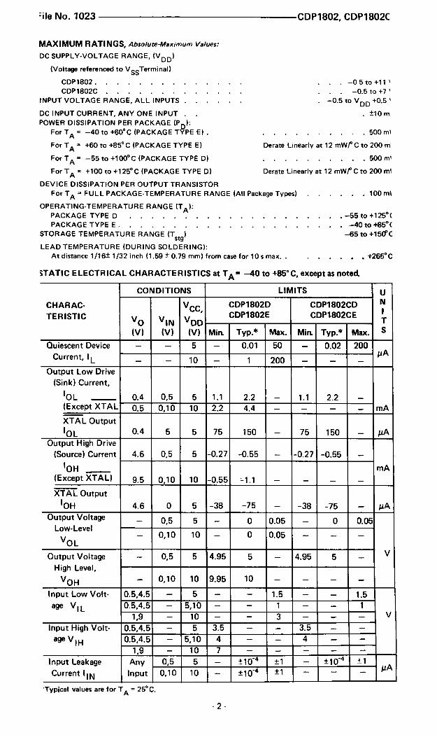
STATIC ELECTRICAL CHARACTERISTICS at TA= ‐ 4 0 to +85°C, except asnoted.
CONDITIONS LIMITS U
CHARAC- Vcc CDP1802D CDP1802CD I).TERISTIC ' CDP1802E CDP1BOZCE
Vo VIN VDD T( V ) (V) (V) Min. Typ.* Max. Min. Typ.* Max. 8
Quiescent Device ‐‐ ‐ 5 ‐ 0.01 50 ‐ 0.02 200 ACurrent, IL _ __ 10 _ 1 200 _ _ _ '1
Output Low Drive(Sink) Current,
'OL 0.4 0,5 5 1.1 2.2 ‐ 1.1 2.2 ‑(_Except XTAL 0.5 0,10 10 2.2 4.4 ‐ ‐ ‐ _ mA
XTAL OutputI0L 0.4 5 5 75 150 ‐ 75 150 ‐ IIA
Output High Drive(Source) Current 4.6 0,5 5 ‐0.27 ‐0.55 ‐ -0.27 ‐0.55 ‑
'OH mA(Except X TA L ) 9.5 0,10 10 ‐o.55 4 . 1 ‐ ‐ _ _
XTAL Output
'0H 4.5 o 5 ‐38 ‐75 ‐ ‐38 -75 ‐ pAOttPUtLW'l‘age ‐ 0,5 5 ‐ o 0.05 ‐ o 0.05
3W eve ‐ 0,10 10 _ o 0.05 ‐ ‐ ‑OL
Output Voltage ‐ 0,5 5 4.95 5 ‐ 4.95 5 ‐ VHigh Level,
vOH ‐ 0,10 10 9.95 10 _ ‐ _ _
Input Low Volt- 0.5,4.5 - 5 - ‐ 1.5 ‐ ‐ 1.5age V”_ 0.5,4.5 ‐ 5,10 ‐ ‐ 1 ‐ ‐ 1
1,9 ‐ 10 ‐ ‐ 3 ‐ ‐ ‐ VInput High Volt- 0.5.4.5 ‐ 5 3.5 ‐ ‐ 3.5 ‐ ‑
age vIH 0.5.4.5 ‐ 5,10 4 ‐ _ 4 _ ‑1,9 ‐ 10 7 ‐ ‐ ‐ ‐ ‑
Input Leakage Any 0,5 5 ‐ :10‘4 :1 ‐ :10'4 :1 ACurrent (IN Input 0,10 10 ‐ :10'4 i1 - - - “
‘Typical values are for TA = 25°C.

CDP1802, CDP1802C File No. 1023
STATIC ELECTRICAL CHARACTERISTICS at TA = ‐ 4 0 to +85°C,except asnoted.
CONDITIONS LIMITS U
CHARAC- VCC CDP1802D CDPIBOZCD TTERISTIC ' CDP1802E CDP18020E
Vo VIN VDD T(V) ( V ) (V) Min. Typ.* Max. Min. Typ.* Max. S
3-State Output 0,5 0,5 5 - 110'4 :1 ‐ :10'4 :1 yALeakage Current 0,10 0'10 10 _ :10“ t1 _ __ __
OUTMinimum Data
V = V - 2 2 4 ‐ 2 2 4 VRetention Volt‐ DD DR
age, VDR
Data Retention VDD = 2.4 V - 0.01 1 -‐ 0.5 5 11ACurrent, IDR
'Typical values are for TA = 25°C.
RECOMMENDED OPERATING CONDITIONS at TA = ‐ 4 0 to + 85° C Unless Otherwise SpecifiedFor maximum reliability, nominaloperating conditions shouldbe selectedsothat operation is always within the fol/owing ranges:
CONDITIONS LIMITS
CHARACTERISTIC VCC1 VDD CDP18OZD CDP1802CD UNITS(V) (V) CDP1802E CDP1802CE
Supply-Voltage Range ‐ ‐ 4 to 10.5 4 to 6.5 V
Input Voltage Range - - VSS to VCC VSS to VCC V
Maximum Clock Input Rise orFall Time, tr or tf 4‐10.5 4‐10.5 1 1 us
5 5 6.4 6.4Instruction Time2 5 10 5 1 _. #5
(See Fig. 8)10 10 3.2 ‑
5 5 312 312
Maximum DMA Transfer Rate 5 10 390 ‐ KBVIES/Sec10 10 625 ‑
5 5 DC ‐ 2.5 DC ‐ 2.5Maximum Clock Input Frequency, 5 10 DC _ 3 1 _ MHzf 3 'CLOCK 1o 10 DC - 5 ‑
NOTES:1: V <V ; f o r CDP1802C, V = V = 5 volts.CC DD . D SC . . .2 . Equals 2 machine cycles ‐ one Fetch a n one Execute o p e r a t i o n fo r all I n s t r u c t i o n s except Long Branch and
Long Skip, which require 3 machine cycles ‐ one Fetch and t w o Execute operations.3. Load Capacitance (CL) = 50 p F.
DRAIN-TO-SOURCE VOLTAGE (VDSI‐V3 - 9 - 8 - ' l - 6 ‐ 5 - 4 - 3 - 2 - l O
VOLTAGE )I IOV
(
E.LI
-9I:z,inKKDU
l a ]40IDO2’.I‘2II‑30.
§o I 2 3 4 5 e 7 a 9 no
DRAIN-TO-SOURCE vomxe: (v05) ‐v
BZCS-SI IGB 9 2 ¢ S - 3 I 8 5 4
Fig. 2 ‐ Minimum o u t p u t high (source) current Fig. 3 ‐ Minimum o u t p u t l o w (sink) currentcharacteristics. characteristics.

File No. 1023 CDP1802, CDP18OZC
AMBIENT TEMPERATURE (TAI ' 25'CAMBIENT TEMPERATURE (TA)= 25-IAI ‘ v iA~ IAImc
II_Jp
_'Ix:I‑
A0“\JNOD-5
5‘
. .0 v . VDD'c h ' AI
SKIS - Z9598
LOAD CAPACITANCE ( C L I ‐ p F 92:5 2 9 5 % xfitgg 9F ALOAD CAPACITANCE ( A C L I ‐ pF
NOTE: ANY OUTPUT ExCEPT ‐xTAL
Fig. 5 ‐ Typical change in propa t ion delay asafunction of a change In oadcapaCItance.
Fig. 4 -‐ Typical transistion time vs. loadcapacitance.
9F. AMBIENT TEMPERATURE (TAI -25 'C
635 75 85 I I5 IZS 2_ 0.01 . I I0
SPEC. AMBIENT TE“PERATURE (TA) 'C CLOCK INPUT FREQUENCY “C I-MN!VALUE , 9 2 6 3 - 2 9 5 ‘ 9A T 509‘; e n s - 2 3 5 w NOTES‑
I D L E : "oo'AT MIOOOOI BRANCH - ' 3701'AT m e l o n CL' 50 pF
Fig. 7 ‐ Typical power dissipation asa function ofclock frequency for BRANCH instructionand I D L E instruction for CDP1802,
Fig. 6 ‐ Typical maximum clock frequency asafunction of temperature.
’CLOCK "HCL: TINSTRUCTION TIME= |6(ICL)= 2 MACHINE CYCLES( E X C E P T LONG BRANCH AND LONG SKIP. WHICHREDUIRE 3 MACHINE C Y C L E S )
I‘cc . 5 T-IP ( C L O C K TO L o w MEMORYADDRESS BYTEI-ISUIDATA S E T U P )
5 6 7 12INSTRUCTION TIME‐,ts
e 5.3 4 3 2 2 67 2.29 2 I 7 8 I»6 L 4 5 l.33CLOCK INPUT FREQUENCY (ICLI‐MHz. 926L-29643
Fig. 8 ‐ Requiredmemory system address time asa function of instruction time.
. 4 .

CDP1802, CDP1802C File No. 1023
v vVOO Vcc on cc
I 1 Von A AINPUTS
INPUTS OUTPUTS‐. 0VDD <‐ ‐> V55N ip ‐ h < ‐ -> +O
Vss ‘ - I ‐> ‑<‐ .‐ - 7
VSS szcs‐zssosE
TEST ANY ONE INPUT WITH ALL OTHERINPUTS AT “NOISE” VOLTAGE LEVELS. v
SS 92C5-29607
Fig. 9 - ”0'39 immunity ‘95" Circuit. Fig. 1 0 - Quiescent-device leakagecurrent testcircuit.
‘I’DD ‘Icc VDD Vcc
INPUTS OUTPUTS
V,» I NOTE- ’ VDDW I MEASURE INPUTS ’o SEOUENTIALLY ‐‑Vss ‘ T OBOTH vDD AND VSS‘ 3 - 5 " ” : _ . V955
<‐ CONNECT ALL UNUSED _. ___,INPUTS TOEITHER OIInggEgD NOTE:
. MEASURE OUTPUTSI VD” 0“ V55 SEOUENTIALLY.
V55 FORCE DEVICE CONNECT ALL UNUSEDINTO DMA OUT INPUTS T0 vDD OR v55.
9 2 c s ‐ 29608 STATE sacs ‐ 29609
F’g- ’1 _ ” ’9 ‘ " leakage 9 “ ” 9 ’ " t 9 “ Ci’CUIt- Fig. 12 ‐ Threestate o u t p u t leakage (data bus)test circuit.
I k o u z s w e v o + + + + + + + + a'w
IWOI I'0 II I20 2| 3° 3I 4° 4) 5° 5| 6° 6| 7° 7|I I|
I 'PLN pHTPA
II I II I II I'PLHI I I'PHL S
|I
I | lwe I I I
' P ‐ I ‐ I§ U‐ ' - I -' H- IMEMORY . 'PLH.' ' HIGH ORDERADDRESS ADDRESS BYTE
| Im IPLH 'PHL
LOW ORDERADDRESS BYTE
(MEMORYREAD CYCLE) I
TMR(MEMORY Iwant: CYCLE) I
DATA FROM // ’PLH-IPHCPU TOBUS
I II I
I I II I rT
STATE "1“» T I I I I1CODES 15: | I l p
l I I I 1
o T ' IPLH-IPHL I I II I I I II T TNO.NI.N2 I I . I I
( I / O ' 5 “ j ' I‘.EXECUTION I I L
E) I I DATA
D a m ///////////flI//////////I////////////////////////X-‐+9mDMA SAMPLED (SI 82 S3)
W I IREQUEST I INTERRWT m
I I s w a m ) ( s I . s2 I I
INTERRUPT I
“ w e " FLAG LINES mSAMPLED ( I N SI) I
F I - 4 ' ' H I I
I 1ANY NEGATIVE
'SU TRANSITION
0CLEAR E 7 ! 9 2 ¢ L - 2 9 5 9 9 R 1
NOTES?1. THIS TIMING DIAGRAM IS USED TO SHOW SIGNAL RELATIONSHIPS 3. SHADED AREAS INDICATE nDON'T CARE" 0R UNDEFINED STATE;
ONLY AND DOES NOT REPRESENT ANY SPECIFIC MACHINE CYCLE MULTIPLE TRANSITIONS MAY OCCUR DURING THIS PERIOD
2‘ ALL MEASUREMENTS ARE REFERENCED TO 50% POINT OF THEWAVEFORMS
Fig. 13 ‐ Timing waveforms.
. 5 .

File No. 1023
DYNAMIC ELECTRICAL CHARACTERISTICS at TA = -‐40 to +85°C, CL = 50 p F,VDD 15%, except as noted.
CDP1802, CDP18OZC
CHARACTERISTICVDD
LIMITSUNITS
(V) (VI Typ. ‘ Max.
Propagation Delay Time, tPLH, tPHL: 5 5 300 450Clock to TPA, TPB 5 10 250 350 ns
10 10 150 2005 5 900 1350
Clock-to-Memory High-Address Byte 5 10 500 750 ns10 10 400 6005 5 350 500
Clock-to-Memory Low-Address Byte 5 10 250 375 ns
10 10 150 2505 5 300 450
Clock to MRD, tPLH 5 10 250 350 ns10 10 150 2005 5 300 450
Clock to Win‐D, tPHL 5 10 250 350 ns10 10 150 2005 5 300 450
Clock to MWR, tPLH, tPHL 5 10 250 350 ns10 10 150 2005 5 450 650
Clock to (CPU DATA to BUS) 5 10 350 450 ns10 10 200 3005 5 500 750
Clock to State Code 5 10 350 450 ns10 10 250 3005 5 350 550
Clock to O 5 10 250 400 ns10 10 150 2505 5 550 800
Clock to N(02), tPLH 5 10 350 500 ns10 10 250 350
Minimum Setup and Hold Times, tSU, tHV 5 5 ‐30 0Data Set Up 5 10 -25 10
10 10 -10 20 ns5 5 200 300
Data Hold 5 10 125 20010 10 100 1505 5 -75 0
W S e t u p 5 1 0 ‐5o 010 10 -25 0 ns5 5 150 250
m Hold 5 10 100 20010 10 75 125
OTypical values are for TA = 25°C and nominal VDD.
VMaximum limits of minimum characteristics are the values above which all devices function.
CDP1802, CDP1802C File No. 1023
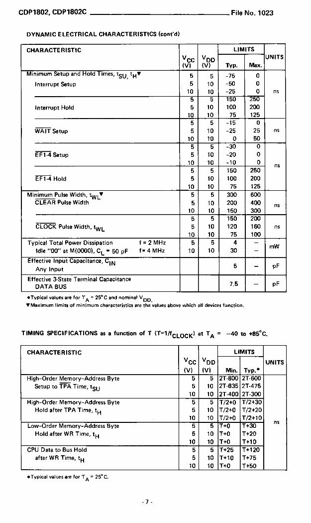
DYNAMIC ELECTRICAL CHARACTERISTICS (cont’d)
CHARACTERISTIC LIMITSVcc VDD UNITS(V) (V) Typ. Max.
Minimum Setup and Hold Times, tSU, tHv 5 5 _75 0
Interrupt Setup 5 10 ‐50 010 10 ~25 0 ns5 5 150 250
Interrupt Hold 5 10 100 20010 10 75 1255 5 -15 0
WAIT Setup 5 10 ‐25 25 ns
10 10 0 505 5 ‐30 0
EF1-4 Setup 5 10 ‐20 O10 10 ‐10 0 n55 5 150 250
EF1-4 Hold 5 10 100 20010 10 75 125
Minimum Pulse Width, tWL' 5 5 300 600CLEAR Pulse Width 5 10 200 400 ns
10 10 150 3005 5 150 200
CLOCK Pulse Width, tWL 5 10 I20 160 ns10 10 75 100
Typical Total Power Dissipation f= 2 MHz 5 5 4 - mWIdle "00" at M(0000), CL = 50 pF f= 4 MHz 10 10 30 ‑
Effective Input Capacitance, CIN 5 F
Any Input _ p
Effective 3-State Terminal CapacitanceDATA BUS 7-5 ‐ F’F
OTypical values are for TA = 25° C and nominal VDDVMaximum limits of minimum characteristics are the values above which all devices function.
TIMING SPECIFICATIONS as a function of T (T=1/fCLOCK) at TA = ‐ 4 0 to +85°C.
CHARACTERISTIC LIMITS
Vcc Voo UNITS(V) (V) Min. Typ . ’
High-Order Memory‐Address Byte 5 5 2T-800 2T-600Setup to W Time, tSU 5 1o 2T-635 2T-475
10 10 2T-400 2T-300High-Order Memory‐Address Byte 5 5 T/2+0 T/2+30
Hold after TPA Time, tH 5 10 T/2+0 T/2+2010 10 T/2+0 T/2+10
Low-Order Memory‐Address Byte 5 5 T+0 T+30 nsHold after WR Time, tH 5 10 T+0 T+2O
10 10 T+0 T+10CPU Data to Bus Hold 5 5 T+25 T+120
after WR Time, tH 5 10 T+10 T+7510 10 T+0 T+50
oTypicaI values are for TA = 25°C.
File No. 1023 CDP1802, CDP18026
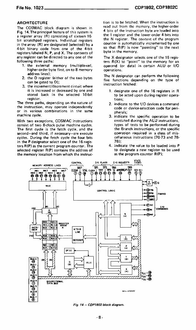
ARCHITECTUREThe COSMAC block diagram is shown inFig. 14.The principal feature of this system isa register array (R) consisting of sixteen 16‑bit scratchpad registers. Individual registersin the array (R) are designated (selected) by a4-bit binary code from one of the 4-bitregisters labeled N, P, and X. The contents ofany register can be directed to any one of thefollowing three paths:
1. the external memory (multiplexed,higher-order byte first, on to 8 memoryaddress lines);
2. the D register (either of the t w o bytescan be gated to D) ;
3. the increment/decrement circuit whereit is increased or decreased by one andstored back in the selected 16-bitregister.
The three paths, depending on the nature ofthe instruction, may operate independentlyor in various combinations in the samemachine cycle.
With t w o exceptions, COSMAC instructionsconsist of t w o 8-clock-pulse machine cycles.The first cycle is the fetch cycle, and thesecond‐and third, if necessary‐are executecycles. During the fetch cycle the four bitsin the P designator select one of the 16 regis‑ters R(P) as the current program counter. Theselected register R(P) contains the address ofthe memory location from which the instruc‑
CONTROL I / O FILAGS
t ion is to be fetched. When the instruction isread o u t from the memory, the higher-order4 bits of the instruction byte are loaded intothe I register and the lower-order 4 bits intothe N register. The content of the programcounter is automatically incremented by oneso that R(P) is now "pointing" to the nextbyte in the memory.
The X designator selects one of the 16 regis‑ters R(X) to "po in t ” to the memory for anoperand (or data) in certain ALU or l/Ooperations.
The N designator can perform the followingfive functions depending on the type ofinstruction fetched:
1. designate one of the 16 registers in Rto be acted upon during register opera‑tions;
2. indicate to the l/O devices a commandcode or device-selection code for peri‑phe'rals;
3. indicate the specific operation to beexecuted during the ALU instructions,types of tests to be performed duringthe Branch instructions, or the specificoperation required in a class of mis‑cellaneous instructions (70-73 and 78‑7B);
4. indicate the value to be loaded into Pto designate a new register to be usedasthe program counter R(P);
STATEI / O REQUESTS CODES
I , ‐ %MEMORY ADDRESS LINES I
7MAIMAO MAZ MA4 MAG
REGISTERARRAY
Rm c n l am.-IDECK
BIDIRECTIGOALDATA BUS
Em
CONTROL LOGIC
\IW:
3‐4
TIMING
N2I / O
COMMANDS
Vcc‐®Von‐9Vss
s z n - z v u s fi z
Fig. 14 ‐ CDP1802 block diagram.
CDP1802, CDP18OZC File No. 1023
5. indicate the value to be loaded into Xto designate a new register to be usedasdata pointer R(X).
The registers in R can be assigned by a pro‑grammer in three different ways: asprogramcounters, as data pointers, or as scratchpadlocations (data registers) to hold t w o bytesof data.
Program CountersAny register can be the main programcounter; the address of the selected registeris held in the P designator. Other registers inRcan beused assubroutine program counters.By a single instruction the contents of the Pregister can be changed to effect a ”cal l ” to asubroutine. When interrupts are being ser‑viced, register R(1) is used as the programcounter for the user's interrupt servicing rou‑tine. After reset, and during 3 DMA oper‑ation, R ( 0 ) is used asthe program counter.At all other times the register designated asprogram counter is at the discretion of theuser.
Data PointersThe registers in R may be used as datapointers to indicate a location in memory.The register designated by X (i.e., R(X))points to memory for the following instruc‑tions (see Table I ) :
ALU operations F1-F5,F7, 74, 75, 77;o u t p u t instructions 61 through 67;input instructions 69 through 6F;certain miscellaneous instructions‐70‑73, 78.60, F0.
The register designated by N (i.e., R(N))points to memory for the ”load D frommemory" instructions 0N and 4N and the"Store D" instruction 5N. The registerdesignated by P (i.e., the program counter) isused asthe data pointer for ALU instructionsF8-FD, FF, 7C, 70 , 7F. During these instruc‑tion executions, the operation is referred toas "data immediate".Another important use of R asa data pointersupports the built-in Direct-Memory-Access(DMA) function. When a DMA-In or DMA‑Out request is received, one machine cycle is"stolen". This operation occurs at the end ofthe execute machine cycle in the currentinstruction. Register R(O) is always used asthe data pointer during the DMA operation.The data is read from (DMA-Out) or writteninto (DMA-In) the memory location pointedto by the R(0) register. At the end of the trans‑
fer, R(0) is incremented by one so that theprocessor is ready to act upon the nex t DMAbyte transfer request. This feature in theCOSMAC architecture saves a substantialamount of logic when fast exchanges ofblocks of data are required, such as withmagnetic discs or during CRT-display-refreshcycles.
A program load facility, using the DMA-Inchannel, is provided to enable users to loadprograms into the memory. This facility pro‑vides a simple, one-step means for initiallyentering programs into the microprocessorsystem and eliminates the requirement forspecialized “bootstrap” ROM’s.
Data RegistersWhen registers in R are used to store bytes ofdata, four instructions are provided whichallow D to receive from or write into eitherthe higher-order- or lower-order-byte portionsof the register designated by N. By thismechanism (together with loading by dataimmediate) program pointer and data pointerdesignations are initialized. Also, this tech‑nique allows scratchpad registers in R to beused to hold general data. By employingincrement or decrement instructions, suchregisters may be used as loop counters.
The 0 Flip FlopAn internal flip flop, O, can beset or reset byinstruction and can be sensed by conditionalbranch instructions. The ou tpu t of Q is alsoavailable asa microprocessor ou tpu t .
Interrupt ServicingRegister R(1) is always used as the programcounter whenever interrupt servicing is ini‑tiated. When an interrupt request comes inand the interrupt is allowed by the program(again, nothing takes place until the comple‑tion of the current instruction) the contentsof the X and P registers are stored in thetemporary register T, and X and P are set tonew values; hex digit 2 in X and hex digit 1in P. Interrupt enable is automatically de‑activated to inhibit further interruptions. Theuser's interrupt routine is now in control; thecontents of T may be saved by means of asingle instruction (78) in the memory locationpointed to by R (X). At the conclusion of theinterrupt, the user's routine may restore thepre-interrupted value of X and Pwith a singleinstruction (70 or 71). The interrupt-enableflip-flop can be activated to permit furtherinterrupts or can bedisabled to prevent them.
COSMAC Register Summary
D 8 Bits Data Register (Accumulator) N 4 Bits Holds Low~0rder Instr. DigitDF 1 Bit Data Flag ( A L U Carry) l 4 Bits Holds High-Order Instr. DigitR 16 Bits 1 of 16 Scratchpad Registers T 8 Bits Holds old X, P after InterruptP 4 Bits Designates which register is (X is high nybble)
Program Counter IE 1 Bit Interrupt EnableX 4 Bits Dsflganggeisnit/zfruch register IS 0 1 Bit Output Flip Flop

File No. 1023 CDP1802, CDP‘IBOZC
INSTRUCTION SET
The COSMAC instruction summary is givenin Table I. Hexadecimal notation is used torefer to the 4-bit binary codes.
In all registers bits are numbered from theleast significant bit (LSB) to the most signi‑ficant bi t (MSB) starting with 0.
R M ) : Register designated by W, where
R(W).0: Lower-order byte of R(W)R(W).1: Higher-order byte of R(W)Operation Notation
M(R(NI I - ’D: R(N)+1->R(N)
This notation means: The memory bytepointed to by R(N) is loaded into D, and
W=N or X, or P R(N) is incremented by 1.
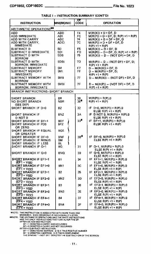
TABLE I ‐ INSTRUCTION SUMMARY(For Notes, see page 13)
OPINSTRUCTION MNEMONIC CODE OPERATION
MEMORY REFERENCELOAD V I A N LDN 0N M(R(N))->D; FOR N NOTOLOAD ADVANCE LDA 4N M(R(N)) ->D; R(N) +19 R(N)LOAD V I A X LDX F0 M(R(X)) '>DLOAD VIA X AND ADVANCE LDXA 72 M(R(X)) ->D; R(X) +1 ~>R(X)LOAD IMMEDIATE LDI F8 M(R(P))+ D; R(P) +1->R(P)STORE V I A N STR 5N D->M(R(N))STORE V I A X A N D STXD 73 D->M(R(X)) ;R(X) ‐1-> R(X)
DECREMENTREGISTER OPERATIONSINCREMENT REG N INC 1N R(N) +1 ->R(N)DECREMENT REG N DEC 2N R ( N ) - 1 + R(N)INCREMENT REG x IRX 60 R ( X ) +1 + R(X)GET LOW REG N GLO 8N R(N).0-> DPUT LOW REG N PLO AN D-> R(N).0GET HIGH REG N GHI 9N R(N).1->DPUT HIGH REG N ” PHI BN D-> R(N).1L IC OPERATIONSciga‘ on F1 mafixnonD+DOR IMMEDIATE ORI F9 M(R(P)) OR 0 - ) D; R(P)+1+ R(P)EXCLUSIVE OR XOR F3 M(R(X)) XOR D-> DEXCLUSIVE OR IMMEDIATE XRI FB M(R(Pl) XOR D+D;R(P)+1+R(P)AND AND F2 M(R(X)) AND D - ) DAND IMMEDIATE ANl FA M(R(P)) AND D + D; R(P)+1+ R(P)SHIFT RIGHT SHR F6 SHIFT D RIGHT, LSB(D)*DF.
0+MSB(D)SHIFT RIGHT WITH SHRC 76. SHIFT D RIGHT, LSBIDPDF,
CARRY % DF+MSBIDIRING SHIFT RIGHT RSHRSHIFT LEFT SHL FE SHIFT D LEFT, MSBIDI+DF,
0->LSB(D)SHIFT LEFT WITH SHLC 7E. SHIFT D LEFT, MSB(D)+DF,
CARRY DF+LSBIDIRING SHIFT LEFT RSHL
ONOTE: THIS INSTRUCTION IS ASSOCIATED WITH MORE THAN ONEMNEMONIC. EACH MNEMONIC IS INDIVIDUALLY L I S T E D ]
”NOTE: THE ARITHMETIC OPERATIONS AND THE SHIFT INSTRUCTIONSARE THE ONLY INSTRUCTIONS THAT CAN ALTER THE DF.AFTER AN ADD INSTRUCTION:
DF =1 DENOTES A CARRY HAS OCCURREDDF = 0 DENOTES A CARRY HAS NOT OCCURRED
AFTER A SUBTRACT INSTRUCTION:DF =1 DENOTES NO BORROW. D I S A TRUE POSITIVE NUMBEROF = OOENOTES A BORROW. D IS TWO'S COMPLEMENTTHE SYNTAX “~INOT D F ) " DENOTES THE SUBTRACTION OF THE BORROW
. 1 0 .
CDP1802, CDP1802C File No. 1023
TABLE I ‐ INSTRUCTION SUMMARY (CONT'DI
(5PINSTRUCTION IMNEMONIC CODE OPERATION
ARITHMETIC OPERATIONS”ADD ADD F4 M(R(X)) + 0+ DF, DADD IMMEDIATE ADI FC M(R(P))+D->DF, D; R(P) +1->R(P)ADD WITH CARRY ADC 74 M(R(X ) )+D+DF->DF,DADD WITH CARRY, ADCI 7C M(R(P)) + D + DF + DF, D
IMMEDIATE R(p) +1S 1111:)SUBTRACT D S D F 5 M ( R ( X ) ) ‐ 0 + D F, DSUBTRACT D IMMEDIATE SDI FD M(R(PI) ‐ D + DF, D; R(P) +1+ R(P)SUBTRACT D WITH SDB 75 M(R(X)) ‐ D ‐ (NOT DF) + DF, D
BORROWSUBTRACT D WITH SDBI 7D M(R(P)) ‐ D ‐_INOT DF) + DF, D;
BORROW, IMMEDIATE R(P) +1 + R(p)SUBTRACT MEMORY SM F7 D _ M(R(X)) + DF, DSUBTRACT MEMORY SMI FF D ‐ M(R(P) ) ->DF,D ;
IMMEDIATE R(P) +1+ R(P)SUBTRACT MEMORY WITH SMB 77 D ‐ M(R(X)) ‐ (NOT DF) + DF, D
BORROWSUBTRACT MEMORY WITH SMBI 7 F D ‐ M ( R ( P ) ) ‐ ( N O T DF)->DF,D
BORROW, IMMEDIATE R(P)+1+ R(P)BRANCH INSTRUCTIONS‐SHORT BRANCH
SHORT BRANCH BR 30 M(R(PI)+ R(P).oNO SHORT BRANCH NBR 38’ RIP) +1 + R(P)
(SEE SKPISHORT BRANCH IF 0 : 0 82 32 IF D=o, M(R(P))-> R(P).o
ELSE R(P) +1 + R(P)SHORT BRANCH IF BNZ 3A IF D NOT 0, M(R(PII+ R(P).o
D NOT 0 ELSE R(P) +1 + R(P)SHORT BRANCH IF DF=1 BDF ? 33’ IF DF=1, M(R(P))-> R(P).oSHORT BRANCH IF POS BPZ ELSE R(P) +1 + R(P)
OR ZEROSHORT BRANCH IF EQUAL BGE
0R GREATERSHORT BRANCH IF DF=o BNF 33’ IF DF=o, M(R(PII‘> R(PI.0SHORT BRANCH IF MINUS BM ELSE R(P)+1+ R(P)SHORT BRANCH IF LESS BLSHORT BRANCH IF 0 : 1 BO 31 IF O=I, M(R(P))-> R(P).o
ELSE R(PI +1 + R(PISHORT BRANCH IF O=o BNO 39 IF O=o, M(R(P))+ R(P).0
ELSE R(P) +1 + R(P)S H E BRANCH IF EF1=1 BI 34 IF EF1=1, M(R(PII+ R(P).0
(EF1= VSS) ELSE R(P) +1 + R(P)SHOiIBRANCH IF EF1=0 BN1 30 IF EF1=0, M(R(P)) + R(P).o
(EF1= v c c ) ELSE R(P) +1 + R(P)SHcm BRANCH IF EF2=1 82 35 IF EF2=1, M(R(P))+ R(P).O
(51:2 = VSS) ELSE R(P) +1 ~>R(P)SHOR_T BRANCH IF EF2=0 BN2 30 IF EF2=o, M(R(P)) + R(P).0
(EF2=Vcc) ELSE R(P) +1+ RIP)SHORT BRANCH IF EF3=1 B3 36 IF EF3=1, M(R(PII + R(P).0
(EF3 = v s s ) ELSE R(P) +1 + R(P)SHOR_T BRANCH IF EF3=0 BN3 3E IF EF3=0, M(R(P))+ R(P).o
(EF3= VCC) ELSE R(P) +1 + R(P)SHORT BRANCH IF EF4=1 B4 37 IF EF4=1, M(R(P))+ R(P).o
(51:4 = V35) ELSE R(P) +1+ R(P)SHORT BRANCH IF EF4=0 BN4 3F IF EF4=0, M(R(P))+ R(P).o
(EF4'= v c c ) ELSE R(P) +1+ R(P)
ONOTE: THIS INSTRUCTION IS ASSOCIATED WITH MORE THAN ONEMNEMONIC. EACH MNEMONIC IS INDIVIDUALLY LISTED.
”NOTE: THE ARITHMETIC OPERATIONS AND THE SHIFT INSTRUCTIONSARE THE ONLY INSTRUCTIONS THAT CAN ALTER THE DF.AFTER AN ADD INSTRUCTION:
DF =1 DENOTES A CARRY HAS OCCURREDDF = ODENOTES A CARRY HAS NOT OCCURRED
AFTER A SUBTRACT INSTRUCTION:DF =1 DENOTES NO BORROW. D IS A TRUE POSITIVE NUMBEROF = 0 DENOTES A BORROW. D IS TWO'S COMPLEMENTTHE SYNTAX " ‐ ( N O T D F ) " DENOTES THE SUBTRACTION OF THE BORROW
. 1 1 .

File No. 1023 CDP1802, CDP18026
TABLE I ‐- INSTRUCTION SUMMARY (CONT'DI
OPINSTRUCTION MNEMONIC CODE OPERATION
BRANCH INSTRUCTIONS‐LONG BRANCH
LONG BRANCH LBR C0 M(R(P))+ R(P).1M(R(P) +1) » R(P).0
NO LONG BRANCH NLBR CS’ R(P) +2» R(P)(SEE LSKP)
LONG BRANCH IF D=0 LBZ 02 IF D=0, M(R(P))+ R(P).1M(R(P) + 1 ) » R(P).0
ELSE R(P) +2» R(P)LONG BRANCH IF D NOT 0 LBNZ CA IF D NOT 0, M(R(P))+ R(P).1
M(R(P) + 1 ) » R(P).0ELSE R(P) +2» R(P)
LONG BRANCH IF DF=1 LBDF c3 IF DF=1, M(R(P))+ R(P).1M(R(P) + 1 ) » R(P).0
ELSE R(P) +2» R(P)LONG BRANCH IF DF=O LBNF CB IF DF=0. M(R(P))+ R(P).1
M(R(P) + 1 ) » R(P).0ELSE R(P) +2» R(P)
LONG BRANCH IF O=1 LBQ c1 IF O=1. M(R(P))+ R(P).1M(R(P) + 1 ) » R(P).0
ELSE R(P) +2_» R(P)LONG BRANCH IF O=0 LBNO ( : 9 IF 0=0.M(R(P))+ R(P).1
M(R(P) +1) » R(P).0ELSE R(P) +2» R(P)
SKIP INSTRUCTIONSSHORT SKIP SKP 38‘ R(P) +1 » R(P)
(SEE NBR)LONG SKIP LSKP CB’ R(P) +2» R(P)
(SEE N L B R )LONG SKIP IF D=0 Lsz CE IF D=0, R(P) +2» R(P)
ELSE CONTINUELONG SKIP IF D NOT 0 LSNZ cs IF D NOT 0, R(P) +2» R(P)
ELSE CONTINUELONG SKIP IF DF=1 LSOF CF IF DF=1, R(P) +2» R(P)
ELSE CONTINUELONG SKIP IF DF=0 LSNF C7 IF DF=0, R(P) +2» R(P)
ELSE CONTINUELONG SKIP IF O=I LSO CD IF O=1, R(P) +2» R(P)
ELSE CONTINUELONG SKIP IF O=o LSNO cs IF O=o, R(P) +2» R(P)
ELSE CONTINUELONG SKIP IF IE=I LSIE CC IF IE=1,R(P)+2» R(P)
ELSE CONTINUECONTROL INSTRUCTIONSIDLE IDL ooFF WAIT FOR DMA OR
INTERRUPT; M(R(O) » BUSNO OPERATION NOP C4 CONTINUESET P SEP ON N » PSET x SEX EN N » xSET 0 SEO 73 1» ORESET 0 RED 7A 0» OSAVE SAV 78 T» M(R(X))PUSH X,P TO STACK MARK 79 (x,P) » T; (X,P) » M(R(2))
THEN P» x; R(2),‐1» R(2)
RETURN RET 7o M(RIIEXIIHXPI; R(X)+1+ Rm1 -)
DISABLE DIS 71 M(R(x)) 9 (x,P); R(X) +1 » R ( x )0->IE
#An idle instruction initiates a repeating S1cycle. The processor will continue to idleuntil an I/O request (INTERRUPT, DMA-IN, or DMA-OUT) is activated. When therequest is acknowledged, the IDLE cycle is terminated and the l/O request is serviced,and then normal Operation is resumed.
ONOTE: THIS INSTRUCTION IS ASSOCIATED WITH MORE THAN ONEMNEMONIC , EACH MNEMONIC IS INDIVIDUALLY LISTED.
. 1 2 .

CDP1802, CDP1802C
TABLE I ‐ INSTRUCTION SUMMARY (CONT'D)
File No. 1023
0PINSTRUCTION MNEMONIC CODE OPERATION
INPUT-OUTPUT BYTE TRANSFEROUTPUT 1 OUT1 61 M(R(X))*BUS; R ( X ) +1->R(X); N LINES=1OUTPUT 2 OUT 2 62 M(R(X))*BUS; FI(X) +1 ->R(X); N LINES= 2OUTPUT 3 OUT 3 63 M(R(X))*BUS,‘ R(X) +1 +R(X) ; N LINES = 3OUTPUT 4 OUT 4 64 M(R(X))+BUS; R ( X ) +1 +R(X) ; N LINES = 4OUTPUT 5 OUT 5 65 M(R(X))"BUS; R(X) +1 ->R(X); N LINES= 5OUTPUT 6 OUT 6 66 M(R(X))+BUS; FHX) +1->R(X); N LINES= 6OUTPUT 7 OUT 7 67 M(R(X))+BUS; R(X) +1 +R(X) ; N LINES= 7INPUT 1 INP 1 69 BUS+M(R(X)); BUS’D; N LINES = 1INPUT 2 INP 2 6A BUS+M(R(X)); BUS+D; N LINES = 2INPUT 3 INP 3 68 BUS+M(R(X)); BUS+D; N LINES = 3INPUT 4 INP 4 6C BUS~>M(R(X)); BUS*D; N LINES = 4INPUT 5 INP 5 6D BUS->M(R(X)); BUS+D; N LINES = 5INPUT 6 INP 6 6E BUS+M(R(X)); BUS+D; N LINES = 6INPUT 7 INP 7 BF BUS*M(R(X)); BUS->0; N LINES = 7
1. Long-Branch, Long-Skip and No Op instructions are the on ly instructions that requirethree cycles to complete (1 fetch + 2 execute).
Long-Branch instructions are three bytes long. The first byte specifies the condition tobe tested; and the second and third byte, the branching address.The long-branch instructions can:
a) Branch unconditionallyb) Test for D=0 or D i Oc) Test for DF=O or DF=1d) Test for O=O or O=1e) effect an unconditional no branch
If the tested condition is met , then branching takes place; the branching address bytesare loaded in the high-and-Iow-order bytes of the current program counter, respectively.This operation effects a branch to any memory location.If the tested condition is n o t met , the branching address bytes are skipped over, andthe nex t instruction in sequence is fetched and executed. This operation is taken forthe case of unconditional no branch (NLBR).
The short-branch instructions are t w o bytes long. The first byte specifies thecondition to be tested, and the second specifies the branching address.The short-branch instruétions can:
a) Branch unconditionallyb) Test for D=0 or D#=0c) Test for DF=0 or DF=1d) Test for O=O or O=1e) Test the status (1 or 0) of the four EF flagsf) Effect an unconditional no branch
If the tested condition is met , then branching takes place; the branching address byteis loaded into the low-order byte position of the current program counter. This effectsa branch with the current 256-byte page of the m e m o r y, i.e., the page which holds thebranching address. If the tested condition is n o t met , the branching address byte isskipped over, and the n e x t instruction in sequence is fetched and executed. This sameaction is taken in the case of unconditional no branch (NBR)
The skip instructions are one byte long. There is one Unconditional Short-Skip (SKP)and eight Long-Skip instructions.The Unconditional Short-Skip instruction takes 2 cycles to complete (1 fetch + 1 execute).Its action is to skip over the byte following i t . Then the next instruction in sequence isfetched and executed. This SKP instruction is identical to the unconditional no-branchinstruction (NBR) except that the skipped-over byte is n o t considered part of the program.The Long-Skip instructions take three cycles to complete (1 fetch + 2 execute).They can:
a) Skip unconditionallyb) Test for D=0 or D960 d) Test for 0 : 0 or O=1c) Test for DF=0 or DF=1 e) Test for |E=1
If the tested condition is met , then Long Skip takes place; the current program counteris incremented twice. Thus t w o bytes are skipped over and the next instruction in sequenceis fetched and executed. If the tested condition is n o t met , then no action is taken.Execution is continued by fetching the n e x t instruction in sequence.
- 1 3 .
File No. 1023
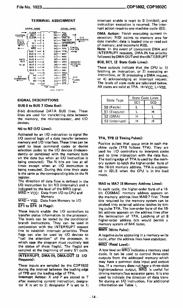
TERMINAL ASSIGNMENT
SIGNAL NAME flGNAL u m ;‐0 CLOCK | 4 0 ‐ V00
CONTROL WAIT 2 s s ‐ x ‘ r r i . ‐ *‐’ CLEAR 3 as ‐ ON I Rag/(EMS‘‐ ‐ DMA ou USTATE 0 4 37 ‐‐ +‑c ozs SCI 5 3 6 ‐ INTERRUPT
sco s 3 5 ‐ W W “ M I N G‐ MRD 7 34 ‐ TPA J. PULSES
B u s 7 a 3 3 ‐ res _ .eus s ‐; 9 3 2 ‐ MA7S U S S ‐ ( I O s I ‐ a n
DATA _ eus 4 ‐ ‐ I ll 3 0 ‐ msBUS B u s 3 ‐« I2 2 9 ‐ MA4 MEMORY
H B u s 2 ‐ _ l 3 2 3 ‐ MAE) ADDRtSSaus I ‐ I4 2 1 ‐ MAZ
Lauso‐Is 2 6 ‐ M A IVcc ‐1|G 2 5 ‐ MAO
U 0 N Z‐ I 1 2 4 ‐ EFTCOMMANDS N' ‐l '8 L 3 ‘ ‐ :‘n no
‐ No [9 22 EF_3 FLAGSvss 20 2| an
TOP VIEW9265727‘67RI
SIGNAL DESCRIPTIONS
BUS 0 to BUS 7 (Data Bus):
8-bit directional DATA BUS lines. Theselines are used for transferring data betweenthe memory, the microprocessor, and Hodevices.
NOto N2 ( l /O Lines):
Activated by an l/O instruction to signal thel/O control logic of a data transfer betweenmemory and l/O interface.These lines can beused to issue command codes or deviceselection codes to the I/O devices (indepen‑dently or combined with the memory byteon the data bus when an l/O instruction isbeing executed). The N bits are low at alltimes except when an l/O instruction isbeing executed. During this time their stateis the same asthe corresponding bits in the Nregister. _The direction of data flow is defined in thel/O instruction by bit N3 (internally) and isindicated by the level of the MRD signal.MRD = Vcc: Data from I/O to CPU and
MemoryMRD = Vss: Data from Memory to Ho
EF1toE‐F4 (4 Flags):
These inputs enable the l/O controllers totransfer status information to the processor.The levels can be tested by the conditionalbranch instructions. They can be used inconjunction with the INTERRUPT requestline to establish interrupt priorities. Theseflags can also be used by HG devices to”call the attention” of the processor, inwhich case the program must routinely testthe status of these flag(s). The flag(s) aresampled at the beginning of every $1 cycle.
INTERRUPT, DMA-IN, DMA-OUT (3 I/ORequests):
These inputs are sampled by the CDP1802during the interval between the leading edgeof TPB and the leading edge of TPA.Interrupt Action: X and P are stored in Tafter executing current instruction; designa‑to r X is set to 2; designator P is set to 1;
- 1 4 .
CDP1802, CDP18026
interrupt enable is reset to 0 (inhibit); andinstruction execution is resumed. The inter‑r u p t action requires one machine cycle (53).
DMA Action: Finish executing current in‑struction; R(O) points to memory area fordata transfer; data is loaded into or read outof memory: and increment R(0).Note: In the event of concurrent DMA andINTERRUPT requests, DMA-IN has priorityfollowed byDMA-OUTand thenlNTERRUPT8C0, $01, (2 State Code Lines):
These outputs indicate that the CPU is: 1)fetching an instruction, or 2) executing aninstruction, or 3) processing a DMA request,or 4) acknowledging an interrupt request.The levels of state code are tabulated below.All states are valid at TPA. H=VCC, L=Vss,
State Type State Code LinesSCI 500
$0 (Fetch) L L81 (Execute) L H
82 (DMA) H L
S3 (Interrupt) H H
TPA, TPB (2 Timing Pulses):
Positive pulses that occur O n c e in each ma‑chine cycle (TPB follows TPA). They areused by l/O controllers to interpret codesand to time interaction with the data bus.The trailing edge of TPA is used by the mem‑ory system to latch the higher-order byte ofthe 16-bit memory address. TPA is suppress‑ed in IDLE when the CPU is in the loadmode.
MAO to MA7 (8 Memory Address Lines):
In each cycle, the higher-order byte of a 16‑bit COSMAC memory address appears onthe memory address lines MAO-7 first. Thosebits required by the memory system can bestrobed into external address latches by tim‑ing pulse TPA. The low-order byte of the 16‑bit address appears on the address lines afterthe termination of TPA. Latching of all 8higher-order address bits would permit amemory systemof 64K bytes.
MWR (Write Pulse):
A negative pulse appearing in a memory-writecycle, after the address lines have stabilized.
MRD (Read Level):
A low level on MRD indicates a memory readcycle. It can be used to control three-stateoutputs from the addressed memory whichmay have a common data input and ou tpu tbus. If a memory does not have a three-statehigh-impedance output, MRD is useful fordriving memory/bus separator gates. It is alsoused to indicate the direction of data trans‑fer during an I/O instruction. For additionalinformation see Table I.
CDP1802, CDP18026 I ' l l e N 0 . ’ IUZS
0:
Single bit output from the CPU which canbe set or reset under program control. Dur‑ing SEQ or REO instruction execution, O isset or reset between the trailing edge of TPAand the leading edge of TPB.
CLOCK:Input for externally generated single-phaseclock. A typical clock frequency is 6.4 MHzat VCC=VDD=10 volts. The clock is count‑ed down internally to 8 clock pulses per ma‑chine cycle.
XTAL:Connection to be used with clock input ter‑minal, for an external crystal, if the on-chiposcillator is utilized. The crystal is connectedbetween terminals 1 and 39 (CLOCK andX TA L ) in parallel with a resistance (10megohms typ.). Frequency trimming capaci‑tors may be required at terminals 1 and 39.For additional information see lCAN-6565.
WAIT, CLEAR (2 Control Lines):
Provide four control modes as listed in thefollowing truth table.
CLEAR vaTT MODEL L LoadL H ResetH L PauseH H Run
The function of the modes are defined asfollows:LoadHolds the CPU in the IDLE execution stateand allows an l/O device to load the memorywithout the need for a "bootstrap” loader. Itmodifiesthe IDLEcondition sothat DMA-INoperation does no t force execution of thenext instruction.ResetRegisters I, N, O are reset, IE is set and 0’s(Vss) are placed on the data bus. TPA andTPB are suppressed while reset is held andthe CPU is placed in S1. The first machinecycle after termination of reset is an initializa‑tion cycle which requires 9 clock pulses. Dur‑ing this cycle the CPU remains in $1 and re‑gisters X, P, and R(0) are reset. Interrupt andDMA servicing are suppressed during theinitialization cycle. The next cycle is an $0,$1, or an 52 but never an $3 . With the use ofa 71 instruction followed by 00 at memorylocations 0000 and 0001, this feature may beused to reset IE, so asto preclude interruptsuntil ready for them. Powerup reset can berealized by connecting a buffered RC net‑work to CLEAR. For additional informationsee lCAN-6581.
Pause
Stops the internal CPU timing generator onthe first negative high-to-low transition of theinput clock. The oscillator continues to oper‑ate, but subsequent clock transitions are ig‑nored.
RunMay be initiated from the Pause or Resetmode functions. If initiated from Pause, theCPU resumes operation on the first negativehigh-to‐low transitiOn of the input clock.When initiated from the Reset operation, thefirst machine cycle following Reset is alwaysthe initialization cycle. The initializationcycle is then followed by 3 DMA ($2) cycleor fetch ($0) from location 0000 in memory.
VDD, VSSI VCC (Power Levels):
The internal voltage supply VDD is isolatedfrom the Input/Output voltage supply Vccso that the processor may operate at maxi‑mum speed while interfacing with variousexternal circuit technologies, including T2Lat 5 volts. VCC must be less than or equal toVDD. All outputs swing from VSS to VCC.The recommended input voltage swing is VSSto VCC.
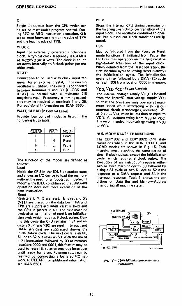
RUN-MODE STATE TRANSITIONS
The CDP1802 and CDP1802C CPU statetransitions when in the RUN, RESET, andLOAD modes are shown in Fig. 15. Eachmachine cycle requires the same period oftime, 8 clock pulses, except the initializationcycle, which requires 9 clock pulses. Theexecution of an instruction requires eithertwo or three machine cycles, 50 followed bya single 81 cycle or two S1 cycles. S2 is theresponse to 3 DMA request and S3 is theinterrupt response. Table II shows the con‑ditions on Data Bus and Memory-Addresslines during all machine states.
MA I T-L o5 em
I LE'D‐ATY :53:
52 5| DMA-INT 53em m / o u r :xscurz mrzeeurr
c c h : CYCLE CYCLEmu
om . m e o ” (IDLE+LOADl-DUAW1’J4
DMA
"47- m . LOAF s a c s - n u n :
Fig. 15 - CDP1802 microprocessor staterransistions.

CDP1802, CDP18026
6 7 0 I 7 3 4 5 6 7 0 I 2 3 I
m m W
m m [ ‐ 1 H m mGENERALTIMING
m [ ‐ 1 1‐1 J’" l m
3:335 | CVCLE n ] CYCLE 1n. I) | CYCLE (n.2| [ c h L E (n.3) | CVCLE Ino0
MA HIGH ADDI Low ADDRESS FIGHADDI L o w ADDRESS inc“ ADD] L o w ADDnEss MGM ADD] L o w ADDRESS FoxADD|
Tusmucncm FETCH 150) | ExECuTE ( s n 1 FETCH (sou [ EXECUYE I 5 ! ) 1 FETCH (so)
, MEMORY[n‐MEMoav READ CYCLE+NON-MEMORV CYCLE ‐+‐MEMDRV AEAD CVCLE ‐ ‐ . . ‐ ‐ ~oNMEMORY CVCLE‐+‐ MADCYCLE
NON. MAD mMEMOEYSI CYCLE _
1 w k I m a m
MEMORY . AL c u m " . VA’ l / / / / / / / / / / / /Al ’ lAV/I/ l / I l / I / l / IAI ’ / / / / / l
‘ ‐ ‐ h ‘ ‐ DALLOWABLE MEMORY ACCEss VA L I D OUYPUT VALID OUYPUT
fismucnou 1 FETCH (so) ] ExECuTE I s u ] FETCH (SO) [ ExEcuTE ( S I ) I FETCH (so)
F‐MEMORV READ CYCLE v‐DF‐MEMORVWRITE CVCLE‐b'i‐ MEMORY READCVCLE‐+‐ MEMORY WRITE CVCLE‐Dk‐ISEEMSRYm I I | | CVCLE
MEMORY __m e E u m I ISI CYCLE L]
2
MEMORY , ,0 0 m " ; V/A'l/I/I/I/I/I/I/AI ”AV/ I l l / l / I / l / IA I W
‘ ‐ § ‘ ‐ DALLOIIABLE MEMORY ACCEss VALID OUTPUT VALID OUTPUT
CPU OUYPUTTo OFF T VA L I D DATA | OFF ] VALID D ATA 1 or :
__MEMORV
WSTRUCTIDN l FETCH ( s o ; I EXECU‘IE ( S I ! [ FETCH (SO) I EXECUTE ( S M | FEYCH (SDI
k‐MEMORV READ CYCLE‐*‐‐ MEMORY READ CVCLE‐+‐‐ MEMORY READ CVCLE+MEMORV READ CVCLE‐+‐ :31ng:33" MT“) fl [ ‐ 1 fl r ‐ I [ ‐ 1 CVCLE
SI CYCLEa _
uwn I m a m
MEMORV ‑L m m W y a m y A - V / y a 7/4?”I , . ‘ _ ‐ ‐ >
ALLOWABLE MEMORY ACCEss VALID OUTPUT L VALID OUTPUT L VALID OUTPUT VALID OUTPUT
Wsmucnon J FETCH (so; [ ExEcuTE «Sn 1' ExEcuTE (SI ) | FEI’CH «sol [EXECUTE 151)
I . ‐MEIIIIonv READ CYCLE ‐ + ‐MEMORY READCVCLE *‐ MEMORY READ CVCLE *‐MEMORV AEAD CYCLE‐+‐‐ Maggi"Lone m I I | | | | j CVCLEBRANCH.LONGSKIP _CVCLE mwn ( H I G H )
Ausuonv( m m W A W /,T W A ' 4 7_ 6 ‐ . 4m
ALLOWABLE MEMORY ACCESS LVAUDOUTPUT
VIA “Don‘I Cue" o! Inlevnal delays - HIgL-Impedancz slate
< ‐ ‐ ‐ ‐ ‐ ‐ ‐ ‐ ‐ ‐ DVAUD OUTPUY LVALIDOUTPUT
92CL-29600
Fig. 16- Timing diagram for machine cycle t y p e Nos. 1, 2, 3, and 4 (propagation delay: n o t shown).
-16 ‑

CDP1802, CDP1802C File No. 1023
TPB J ‐ I fl
MACHINE CYCLE I CYCLE n I CYCLE (n + 1) I
INSTRUCTION j FETCH (50) I EXECUTE ($1) I
HEB I I
N0 ‐ N2 f N = 9 ‐ F \ ‑
MWR
MEMORYOUTPUT
< ‐ ‐ ‐ ‐ ‐ ‐ ‐ ‐ ‐ ‐ ‐ ‐ ‐ ‐ ‐ >ALLOWABLE MEMORY ACCESS VALID OUTPUT
MEMORY MEMORYREAD CYCLE WRITE CYCLE
'User-generated signal
m "Don't Care" or internal delays.
- High-impedance stase
Fig. 17 ‐ Timing diagram for machine cycle t y p e No. 5 (propagation delays n o t shown).
92CS-2960I
MACHINECYCLE I CYCLE n I CYCLE (n + 1) ]
INSTRUCTION I FETCH ($0) I EXECUTE ($1) I
M I fl J‑N 0 ‐ N 2 I N = 1 _ 7 \
ALLOWABLE MEMORY ACCESS‘ ‐ ‐ _ ‐ ‐ ‐ ‐ ‐ - >
‘ _ ‐ _ ' . L VALID DATA FROM MEMORY ‐ ’ALLOWABLE MEMORY ACCESS VALID OUTPUT
DATA STROBE'
IMRD ~TPB . N) Il MEMORY I MEMORY
READ CYCLE READ CYCLE
‘User-generaled signal
m ”Don't Care" or internal delays.
- High-impedance state
Fig. 18 - Timing diagram for machine cycle t y p e No. 6 (propagation delays n o t shown).
92CS-29602
- 1 7 .

File No. 1023 CDP1802, CDP1802C
o I 2 3 4 5 e 7 o 1 2 3 4 5 e 7 o I 2 3 4 5 e 7 o I 2
“ W W WTPA h r ‐ ‘ m m
" 5 I ‐ L J 1 r ‐ IMACHINECYCLE l CYCLE n [ CYCLE In a I) | CYCLE (n . 2) | CYCLE (n . :I)
'NSTRUCV'ON] FETCH ($0) [ EXECUTE I51) ] D M A I s z ) JFETCHISOI
DMA-IN ' / A y Zfl V
MRD fl I \. _,’ ;
MWR \- - _ _ / L _ lMEMORYOUTPUT - _ ’ / m l
*‐ VALID OUTPUT
I
I E ORY ' MEMORY ' E onv IM M M M# ‐ . ‐ * ‐ READ, WRITE O R‐ " T ‘ ‐ ‐ ‐ ‐ > | ¢ - MEMORYR A Y E WR|TE CYCLEI 5 DC CL I NON-MEMORYCYCLE l IREADCYCLE
‘Usev geneIaIed s.qna| I l '
W/A "Don’lCaIe"OImtemaldelavs - HIahImnedanu-w'e 9 2 c s ‐ 2 9 6 0 3
Fig. 1.9 - Timing diagram for machine cycle t y p e No. 7 (propagation delays n o t shown).
0 1 2 3 4 5 6 7 0 I 2 3 4 5 6 7 0 1 2 3 4 5 6 7 0 1 2 3
C L o c x l n fi n fi n r l | | | | | | | | | | | | | | | | | l | | | ] [ ' | | ' ] | ' | | ‘ ] [ ' | | | | | | | | | | |
TPA _ ] ' _ l l l j l
TPB [ ‐ l [ ‐ 1 r ‐ lMACHINECYCLE | CYCLE n | CYCLE In o I) ] CYCLE In +2) ICYCLE (nv3)
INSTRuCTION I FETCH ( $ 0 ) [ EXECUTE I51 ) I OMA I52) [FETCH Isa)
DMA-OUT‘/ A V / . I V / / /
M R D ‐ l ‐ J L . . _ _ _ _ _ _ _ _ - J L l LMWR ' .__ __ J
MEMORYc u m I x x A L - m mDATA' I p VALID DATA FROM MEMORYSTROBE VAL DOUT UT l ‐ l($2~TPB) I I | I
‘ ' MEMORY l 'h__REAfDM€ YRcY E‐ ‐ ‐ . h ‐ ‐ ‐ ‐ READ, WRITE on‐‐*‐REMAEDMCOYRCYLE‐-‐*MEMORY: L : NON-MEMORY CYCLE : IREAD CYCLE
'User‐genevaled mm!
m "Don ' l Care" or Internal delays. - HIgh Impedance s t a l e 926M - 2 9 6 0 4 R |
Fig. 20 ‐ Timing diagram for machine cycle t y p e No. 8 (propagation delay: n o t shown).
0 1 2 3 4 5 6 7 0 1 2 3 d 5 6 7 O 1 2 3 4 5 6 7 0 I 2
C L O C K ] [ ‘ | fi fi fi fl n n n fl n n n fi fi n fl fi n fi n n n n fi n n r
T P “ _ I _ I l _ l _ I | [ ‐ 1 ‑
TPB I _ L [ ‐ 1 r1
MACHINECYCLE 1 CYCLEn 1 CYCLE I n + I ) 1 CYCLE ( n + 2 ) [CYCLE ( r H L I I
INSTRUCTIONL FETCH (SO) 1 EXECUTE (S1) 1 INTERRUPT I53) I FETCH (so)
M R D L ‐ l ' \ . _ _ _ _ _ _ _ _ _ J l
mwn L ‐ ‐ JINTERRUPT' / / 1 _ V //
( INTERNAL) IE ;‑
MEMORY .OUTPUT - f / / / V -7 VIA
‐ VALID OUTPUT
l I | IMEMORY MEMORY READ WRITE‐ * ‐ , ‐ ‐ * ‐ N N-M ‐ . h - MMR Y
READ CYCLE ) OR NON~MEMORY CYCLE | 0 EMORY CYCLE | REAED :VCLEI
'User‘generated SIgnal
m "Don't Care" or Internal dEIays. - Hugh-Impedance slate S Z C M _ 2 9 6 0 5
Fig. 21 ‐ Timing diagram for machine cycle t y p e No. 9 (propagation delays n o t shown).
- 1 3 .

CDP1802, CDP1802C File No. 1023
TABLE I I . CONDITIONS ON DATA BUS AND MEMORY ADDRESS LINES DURING A L L MACHINE STATES
DATA MEMORY __STATE I N MNEMONIC INSTRUCTION OPERATION BUS ADDRESS MRD NOTESG
SI RESET JAM'INOXP=0 I E = 1 RIO) 1 A' ' ' ' ' 0 UNDEFINED
FIRST CYCLE AFTER RESET R I0)ZE: R
NOT PROGRAMMER ACCESSIBLE INITIALI ( O I ‐ 0 0 UNDEFINED 1 B
SO FETCH MIRIP))-*I.N RIP)+1 MIRIPI) RIP) 0 C
o 0 IDL IDLE [Load = 0 (Program IdleI] M IRIO)) R (0) 0 03
[Load = I (Load Mode)] MIRIOI) PREVIOUS 0 E 3ADDRESS '
N950 LDN LOADDVIAN MIRIN))->D MIRIN)) R(N) 0 3
1 N INC INCREMENT R I N ) + I FLOAT R(N) 1 1
2 N DEC DECREMENT R ( N ) ‐ I FLOAT R(N) 1 13 N __ SHORT [BRANCH NOT TAKEN] MIRIPH RIP) 0 3
BRANCH [BRANCH TAKEN] MIRIPII RIP) 0
4 N LDA LOAD ADVANCE MIRIN))-*D R I N ) + I MIRINH R(N) 0 3
5 N STR STORE V I A N D->MIRIN)) D R(N) I 3
0 IRX INC REG X RIXI+1 MIRIX) ) R I X ) 0 3
6 N=1 ‐ 7 OUT N OUTPUT MIRIX)) ->BUS RIXI+1 MIRIXII R I X ) 0 6
I/ON= ‐F I P N I9 N NPUT BUS-rMIRIXI), D DEVICE R I X ) 1 5
MIRIX))->IX.P)0 RET RETURN R(X)+1 ; 1 * ” : MIRIXH R ( X ) 0 3
MIRIX))'*(X,P)1 DIS DISABLE R(X)+1; 0->IE MIRIXII R I X ) 0 3
LOAD VIA X MIRIX))-+D2 LDXA AND ADVANCE R I X ) + 1 M I R I X ) ) R00 0 3
STORE VIA X D->MIRIX) )
3 STXD AND DECREMENT R ( X ) ‐ 1 D RD“ 1 2
7 4,5,7 ‐ ALU OPERATION MIRIXII R I X ) 0 3
6 ‐ ALU OPERATION FLOAT R I X ) 1 1
8 SAV SAVE T->MIRIX)) T R ( X ) 1 2
(X P)->T MIRIZIIA . .9 M R K MARK P - > X ; R ( 2 ) ‐ ‐ I T R I ? ) I 2
51 A REQ RESETQ Q = 0 FLOAT RIP) 1 1
(Exe- B SEQ SET 0 0 =1 FLOAT RIP) 1 1cute) C,D,F ALU OPERATION IMMEDIATE MIRIPII RIP) 0 3
E ALU OPERATION FLOAT RIP) I 1
8 N GLO GET LOW R I N ) .O‐>D R(N) .0 R ( N ) 1 1
9 N GHI GET HIGH R(N) .1->D R ( N ) .1 R(N) 1 1A N PLO PUT LOW D - * R ( N ) . 0 D R I N ) 1 1
B N PHI PUT HIGH D - ’ R ( N ) . 1 D R I N ) 1 1
0'1'2 LONG3.8.9 BRANCH [BRANCH NOT TAKEN] MIRIPII RIP) 0 4AB [BRANCH TAKEN] MIRIP) ) RIP) 0 4
C 3:53-75 LONG [SKIP NOT TAKEN] M I R I P I ) RIP) 0 4IF. SKIP [SKIP TAKEN] MIRIPII RIP) 0 4
4 NOP N0 OPERATION NO OPERATION MIRIPII RIP) 0 4
N SEP SET P N-’P N N R ( N ) 1 1
E N SEX SET X N-*X N N R I N ) I I
O LDX LOAD V I A X MIRIXH‐‘D MIRIXH R I X ) 0 3
1'2: ALU OPERATION M I R I X I ) R ( X ) 0 3
SHIFT D RIGHT6 SHR SHIFT RIGHT _ L S B I D ) " D F 0 » MSB(D) FLOAT R I X ) 1 I
LOADF 8 L 0 ) IMMEDIATE MIRIPH D RIP)+‘I M I R I P I ) R IP) 0 3
9,A,B ALU OPERATIONC,D,F IMMEDIATE MIRIP I ) N P ) 0 3
E SHL SHIFT LEFT A L U OPERATION FLOAT RIP) 1 1
52 IN REQUEST DMA IN BUS->MIRIOII gEVICE R (O) 1 F]
OUT REQUEST DMA OUT MIRIO))->BUS MIRIOH R (0) 0 F3
X.P'*T. 0->|ES3 INTERRUPT 2->X,1->P FLOAT R(N) 1 9
NOTES:A. IE = 1; TPA, TPB suppressed, state = 51 E. Suppress TPA, wait for DMA
B. BUS = O for entire cvcle F. IN REQUEST has prior i ty over OUT REQUEST
C. Next state always 51 G. Numbers refer t o mach ine cyc les t y p e s ‐ re fe r
D. Wait for DMA or INTERRUPT to t i m i n g diagrams, Figs. 16 t h r o u g h 20.
- 1 9 .
File No. 1023 CDP1802, CDP1802C
0 IO 20 30 40 50 60 7O 80 90 IOO IIO I20 I30 I40 ISO ISO I70
0
Dimensions in parentheses are in millimeters andare derived from the basic inch dimensions as in‑dicated. Grid graduations are in mi ls (10 ’3 inch) .
. - i‘ ..
4 - l 0(O-IOZ- 0 - 2 5 4 )
I I I I I I I I l l l l l l
2 3 | - 239( 5 . 8 6 8 - 6 - 0 7 0 )
5le
I 7 5 - I 8 3 j( 4 4 4 5 - 4 5 4 8 ) 7
92CL-29550
The photographs anddimensions of each COS/MOSchip represent a chip when it is p a r t of the wafer.When the wafer is c u t i n t o chips, the cleavageangles are 570 instead of 90° with respect to theface of the chip. Therefore, the isolated chip isactual ly 7 mi ls (0. 17m m ) larger in both dimensions.
Dimensions andpad layout for CDP1802.
. 2 0 .
CDP1802, CDP1802C File No. 1023
OPERATING AND HANDLING Vss to exceed the absolute maximumCONSIDERATIONS rating‑
1. Handling Inpnt SignalsAll inputs and outputs of RCA COS/MOS To prevent damage to the input protec ‑devices have a network for electrostatic t I o n CerUlt. InPUt Signals ShOUld never beprotection during handling. Recom- greater than Vcc " 0 r '655 than VSS‑mended handling practices for COS/MOS Input currents must n o t exceed 10 mAdevices are described in lCAN-6525, 9 V 9 ” When the power SUDP'Y ISOff.“Guide to Better Handlingand Operation Unused Inputsof CMOS Integrated Circuits.” A connection must be provided at every
2. Operating input terminal. All unused input termi‑Operating Voltage nals must be connected to either VCC or
During operation near the 'maximum VSS. whichever '5 appropr ia te .supply voltage limit, care should be Output Short Circuitstaken to avoid or suppress power supply Shorting of outputs to VDD' VCCI orturn-on and turn-off transrents, power VSS may damage COS/MOS devices bysupply ripple, or ground norse; any of . . . . . .these conditions must n o t cause VDD‐ exceeding the maxrmum devrcednssrpatlon.
DIMENSIONAL OUTLINES
(D i SUFFIX (E) SUFFIX40-Lead Dual-ln-Line Side-BrazedCeramic Package
40-Lead Dual-ln‐Line Plastic PackageD _TI A ! ' L M E ‐ C i r ‐ i
sumo u m : l
W I “ ' 1 ‘ " :F'Els_ _ . _ _ a _IIDEX AREA
i°'..2L
L2
'I
E
L J,. . ii Tr: ‐ _ _ 1 T . n ‐ J ‘j _ ‘ R p 11:! u VIEW £1
* 7 " 7 ° “ sziii'iimmed... . 3 " ~=.‐L§' i i .saw-27029111 \ , \
INCHES MILLIMETERS .N HESYMBOL NOTE SYMB°L MIN. MAX. NOTE MIN. MAX.
M'N- MAX- MIN- MAX- A 0.120 0.250 3.10 6.30A 1.980 2.020 50.30 51_30 A1 0.020 0.070 0.51 1.77
a 0.016 0.020 0.407 0.508c 0-095 “ 5 5 3'2: 3'93 B1 0.028 0.070 0.72 1.770 0-017 0-023 - “ 5 5 c 0.008 0.012 1 0.204 0.3041: 0.050REF. 1.27 REF. 0 2.000 2.090 50.00 53.09G o_1oo BSC 1 2.54 380 E1 0.515 0.580 13.09 14.73
H 0.030 0.070 0.76 1.78 '1 °-1 "5 2 2- TrJ 0.008 0 012 3 020 030 0A 0.600 TP 2,3 15.241?
- ' ' L 0.100 0.200 2.54 5.00K 0.125 0.175 3.18 4.45 L2 0,000 0,030 o_oo 0.76L 0.580 0.620 2 14.74 15.74 01 0° 15° 4 0° 15‐5‑M _ 7° _ 7" N 40 5 40
N1 0 6 0I; 0.025 0.050 0.6440 1.27 01 0.065 0095 1.66 2.41
4° 3 0.040 0.100 1.02 2.54seem-27020112 mores: 92cs-30959
NOTES:
1. Laada within 0.005" (0.13m m ) radius of TruePoaitionat maximum material condition.Cantor to cantor of Iaada when formed parallel.When Ulladevice is supplied aoldar dipped, themaximum laad thieltna- (narrow portion)will n o t exceed 0.013" (0.33 mm)
2.3.
When incorporating RCA Solid State Devices inequipment, it is recommended that the designerrefer to "Operating Considerations fo r RCA SolidState Devices", Form No. 1CE-402, available onrequest from RCA Solid State Division, Box 3200,Somerville, N. J. 08876.
Refer to Rules for Dimensioning (JEDEC Publication No. 95)for Axial Lead Product Outlines.1.
- 21 ‑
When this device is supplied solder-dipped, the maximumlead thickness (narrow portion) will n o t exceed 0.013"(0.33 mm) .
. Leads within 0.005" (0.12 mm) radius of True Position(TP) at gauge plane with maximum material conditionand unit installed.
. eA applies in zone L2 when unit installed.
. 0.applies to spread leads prior to installation.
. N is the maximum quantity oi lead positions.
. N1 is the quantity of allowable missing leads.