NEBRASKA NANOSCALE FACILITY NANOFAB/SYNTHESIS …NEBRASKA NANOSCALE FACILITY NANOFAB/SYNTHESIS...
16
NEBRASKA NANOSCALE FACILITY NANOFAB/SYNTHESIS FACILITIES Christian Binek, Professor Department of Physics and Astronomy National Nanotechnology Coordinated Infrastructure University of Nebraska March 22-23, 2016
Transcript of NEBRASKA NANOSCALE FACILITY NANOFAB/SYNTHESIS …NEBRASKA NANOSCALE FACILITY NANOFAB/SYNTHESIS...

NEBRASKA NANOSCALE FACILITYNANOFAB/SYNTHESIS FACILITIES
Christian Binek, ProfessorDepartment of Physics and Astronomy
National Nanotechnology Coordinated InfrastructureUniversity of Nebraska
March 22-23, 2016

NNF Nanofab/Synthesis Facilities
Nanofabrication and clean room• Clean room• Lithography• Etching• Metrology
Nanomaterials and thin film preparation• Thin film deposition• Nanomaterial synthesis• Characterization
2
NNF

NNF Facility for Nanofabrication:Clean Room
3
NNF
Wet etching
Lithography
Dry etching
Metrology
Key features:
• Certified class 10,000 (ISO-7)• 4,000 sq. ft. area with 2,500 sq.
ft. workspace• Real time monitoring system on
harzardous gases, airborneparticle concentration, temperature, air pressure, etc.

NNF Facility for Nanofabrication:Lithography
4
NNF
• Composed with Zeiss SEM and Raithpattern generator
• Energy of electrons: 0.1 ‐ 30 keV• Minimum pattern feature size: ~ 20 nm • Field stitching error ≤ 50 nm
• Instrument for high resolution opticallithography
• Minimum pattern feature size: 0.8µm• Overlay accuracy: ~ 1 µm • Max wafer size: 4 inch (100mm)
E-Beam Lithography System
Mask Aligner System for Optical Lithography (SUSS MJB-4)
Maskless Laser Lithography System (Heidelberg DWL66)
• high resolution pattern generator fordirect writing on wafers
• Minimum pattern feature size: 0.6µm• Overlay accuracy: ~ 0.2 µm • Max wafer size: 6 inch (150mm)
Josephson Junction arraySET deviceNano channel MTJ device Hall bar
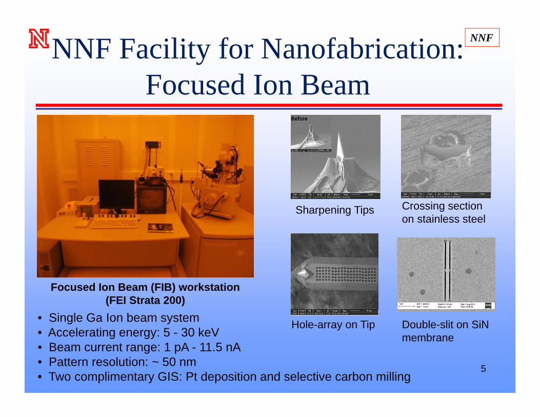
NNF Facility for Nanofabrication:Focused Ion Beam
5
NNF
• Single Ga Ion beam system• Accelerating energy: 5 - 30 keV• Beam current range: 1 pA - 11.5 nA• Pattern resolution: ~ 50 nm• Two complimentary GIS: Pt deposition and selective carbon milling
Focused Ion Beam (FIB) workstation(FEI Strata 200)
Sharpening Tips
Hole-array on Tip
Crossing section on stainless steel
Double-slit on SiNmembrane

NNF Facility for Nanofabrication:Etching
6
NNF
• Versatile R&D ion beam development platform for both thin film milling and deposition
• UHV chamber with base pressure in 10-9 Torr range• one 14cm ion source for ion beam milling • one 4cm ion source for ion beam sputtering
• 9 magnetron sputtering guns for complex thin film stack deposition
• Single axis motion stage with variable incident angle supports multi-angle operation
• The Ending Point Detection system allows users to define etch end point and mount of over etch
Ion Beam Etching System with Ion beam and Magnetron Sputtering
Ti nano-pillars fabricated with Ion beam milling

NNF Facility for Nanofabrication:Etching
7
NNF
• Plasma etch system with ICP and RIE source• Max power: 1000 W – ICP; 600W – RIE• 6 Gas Channels: Ar, O2, CF4, SF6, Cl2, BCl3• Max wafer size: 12 inch (300 mm)
Reactive Ion Etching (RIE) System(Trion Minilock III)
• Offering Si etch solutions for multiple applications• Run Bosch and Cryo etch process• Max RF power: 2000 W – ICP; 400W – RIE• 6 Gas Channels: Ar, C4F8, CF4, CHF3, O2, SF6• Max wafer size: 6 inch (150 mm)
Deep Sillicon Etching System(Oxford PlasmaPro 100)
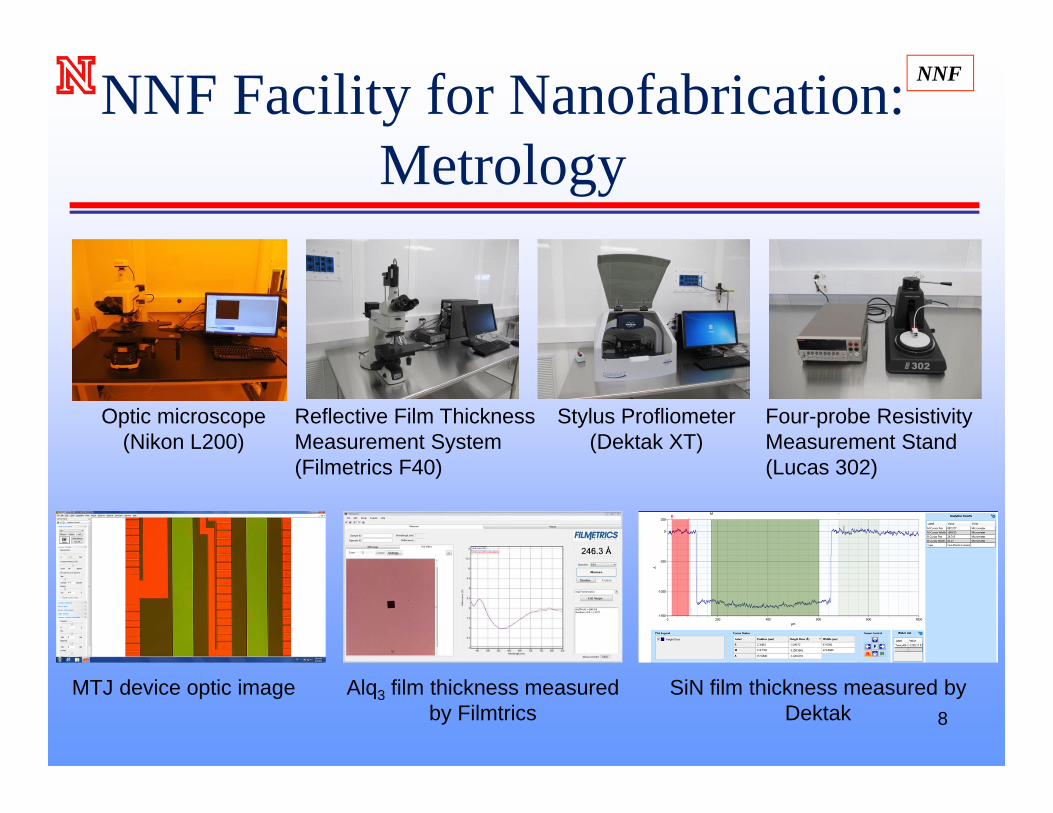
NNF Facility for Nanofabrication:Metrology
8
NNF
Reflective Film Thickness Measurement System (Filmetrics F40)
Stylus Profliometer(Dektak XT)
Four-probe Resistivity Measurement Stand (Lucas 302)
Optic microscope (Nikon L200)
MTJ device optic image SiN film thickness measured by Dektak
Alq3 film thickness measured by Filmtrics

NNF Facility for Nanomaterials and Thin Film Preparation: Thin Film Deposition
9
NNF
Electron beam evaporation systemATC ORION 8000-E (AJA International)
• Base pressure: ~ 2·10-9
Torr• 4 evaporation sources• Substrate heater:
850C max• substrate rotation• Load lock 1 sample• Quartz crystal
thickness monitorAJA Sputtering System
ATC 2000-F (AJA International)
• Base pressure ~ 5·10-8 Torr• Gas environment: Ar & O2• 2RF (300 W) and 2DC (750 W) supplies.• Sputtering source: 5 in total.• Substrates up to 4 inches in diameter• Substrate heater: 850 C max • Substrate rotation and RF bias• Quartz crystal thickness monitor• 6 sample Load lock
TEM image of L10 (Fe,Co)Pt-based magnetic films deposited by AJA sputtering system

NNF Facility for Nanomaterials and Thin Film Preparation: Thin Film Deposition
10
NNF
Pulsed-Laser Deposition
Hex Deposition System
• Base pressure: ~ 1.5· 10-8 Torr• Clean, Inert, Reactive/mixture• Laser raster• 6 targets• Target rotation, raster• Substrate heating 950 C• In-situ RHEED thickness monitor• Load lock - 2 samples• substrate rotation• Combinatorial Films
• System has one DC sputtering gun, thermal evaporator, mini E-beam evaporator and an organic evaporator
• Any 3 deposition techniques can be used simultaneously
• Pressure ~ 4·10-6 mbar in 25min• Pressure ~ 2·10-7 mbar in 16-18 hrs.

NNF Facility for Nanomaterials and Thin Film Preparation: Synthesis
11
NNF
Arc MelterABJ-338 Bell Jar Arc-
Melting Furnace Melt Spinner
• Operating temperature over 3500°C.
• Arc casting• Powder melting• Annealing• Crucible welding• Material densification• Metallic buttons• Spring splat cooling• Creating alloys• High purity melts
• Rapid Solidification from melt, stabilization of metastable phases, microstructure control.
• Laboratory scale system uses 5 to 10 g per run
• Copper spinning wheel ø 200 mm
• Wheel surface speeded up to 60m/s (at 98Hz)
• Crucibles: boron nitride or quartz, with slit nozzle or round nozzle
• Produces ribbons of width 1 -10 mm
Melt-Spun MnBi Ribbons (2-3 mm wide, 70 m thick)Induction-Melted Bi ingot 16 mm dia., 6 mm high
NNF Facility for Nanomaterials and Thin Film Preparation: Synthesis
12
NNF
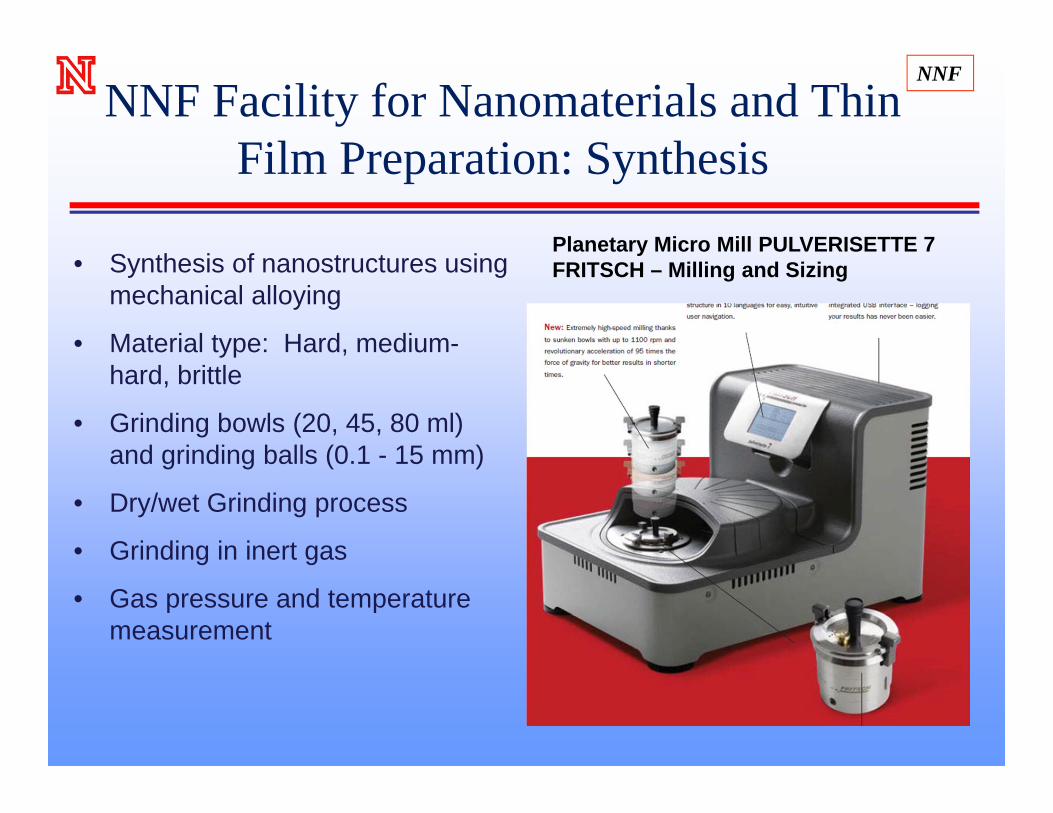
Planetary Micro Mill PULVERISETTE 7FRITSCH – Milling and Sizing• Synthesis of nanostructures using
mechanical alloying
• Material type: Hard, medium-hard, brittle
• Grinding bowls (20, 45, 80 ml) and grinding balls (0.1 - 15 mm)
• Dry/wet Grinding process
• Grinding in inert gas
• Gas pressure and temperature measurement

NNF Facility for Nanomaterials and Thin Film Preparation: Synthesis
13
NNF
Annealing Furnace Compact Vacuum Tube Furnace • Lindberg 55322 oven is a Split-Hinge
Single Zone Furnace with a Tmax = 1200 °C and a working tube of diameter 2.5 inches
• Base pressure ~ 10-6 Torr• Gas environment: Ar / O2 / N2 / Forming
gas• Air annealing• Lindberg 54233 tube oven has an
operating temperature of Tmax = 1500 °C and a working tube of diameter 2 inches
• MTI 1750C max Compact Vacuum Tube• Single Zone Furnace with a Tmax = 1750
°C for 2 Hrs, • 1700°C continuous• Max Heating rate 10 °C/min• 2 in tube diameter • Base pressure ~ 10-6 Torr• Gas environment: Ar / O2 / N2 / Air
annealing

NNF Facility for Nanomaterials and Thin Film Preparation: Characterization
14
NNF
• EverCool®1
• SQUID Sensitivity ~100 nemu
• Temperature Range: 2 - 360K
• 7 Tesla Magnet
• Measurements possible magnetic moment Vs Temperature( ZFC-FC), susceptibility, moment Vs magnetic Field (hysteresis loops)
Quantum Design MPMS XL
Hysteresis Loops
0 50 100 150 200 250 300 350 400
112
114
116
118
120
122
124
126
128
130
Mom
ent (
emu/
g)
Temp (K)
ZFC FC (500 Oe)
-2000 -1500 -1000 -500 0 500 1000 1500 2000-200
-150
-100
-50
0
50
100
150
200
Mom
ent (
emu/
g)
H (Oe)
10K 300K
ZFC–FC measurements
Arc melted Alloy Sample: Fe(3.663g), Co( 1.4881g), Ce (1.1819g), Ti (0.4047g)

NNF Facility for Nanomaterials and Thin Film Preparation: Characterization
15
NNF
ASAP 2460 Surface Area and Porosity Analyzer• Uses Brunauer, Emmett and Teller (BET)
technique determine the surface area of powders and porous materials.
• Applications: Pharmaceuticals, Ceramics, Nanotubes, Adsorbents, Fuel Cells, Paints and Coatings, Activated Carbons and etc.
• 6 sample prep and measurement ports.
• Fully automated modular system optimized for walk-up sample screening

NNF WORKSHOP
The End
Thank You !
16
NNF