NDAQ Electronics Box Front-Panel Interfaces Table Of Contents · PDF fileNDAQ Electronics Box...
41
Printed: 9/3/2013 Serial / Analog Interface Panel Table-Of-Contents 1/41 NDAQ Electronics Box Front-Panel Interfaces Table Of Contents General Information: .................................................... 3 File Reference:................................................................................................................................... 3 Fuses: .................................................................................................................................................. 3 Sensor Power / FETs: ....................................................................................................................... 4 Speed vs NDAQ Cable Lengths: ...................................................................................................... 5 NDAQ External Cable: .................................................................................................................... 7 NDAQ Cable Power vs Voltage Drop: ............................................................................................ 7 Bulgin Pin Assignments: .................................................................................................................. 7 Serial / Analog Panel: ................................................... 8 Emerald DMM-8 Board Layout / Jumpers .................................................................................... 8 Sensor Specific Wiring: .................................................................................................................... 9 CSAT-3 Sonic ................................................................................................................................ 9 Garmin GPS .................................................................................................................................. 9 MaxStream XBee / Xtend Radio Modems .................................................................................. 9 Niwot08 TelosB PAR-Mote-Box, Tsoil-Mote-Box, Mote-Repeater-Box................................ 10 RMY 9101 PropVane Anemometer .......................................................................................... 10 NCAR TRH ................................................................................................................................. 10 Generic Serial Wiring: ................................................................................................................... 12 Power Options ............................................................................................................................. 12 TVS Use / Shielding .................................................................................................................... 12 RS232 ........................................................................................................................................... 12 RS422 ........................................................................................................................................... 12 RS485 ........................................................................................................................................... 12 SIO Interface Panel – Component Current / Power Capacity: .................................................. 13 PCBoard: ......................................................................................................................................... 14 Layout: ............................................................................................................................................. 15 Schematic:........................................................................................................................................ 16 VIPER CPU Panel: ..................................................... 17 Arcom VIPER Board Layout / Jumpers ...................................................................................... 17 Device Specific Wiring: .................................................................................................................. 18 System Console to PC ................................................................................................................. 18 Terabeam EtherAntIII-LR ........................................................................................................ 18 Signal Engineering SE12xx GOES Transmitter ...................................................................... 18 Garmin GPS – With PPS Mapper............................................................................................. 19 Viper DIO Interface Mapper ..................................................................................................... 20 COM-1: ............................................................................................................................................ 21 COM-2: ............................................................................................................................................ 21 COM-3: ............................................................................................................................................ 22 COM-4: ............................................................................................................................................ 22 COM-5: ............................................................................................................................................ 22 USB Errata: ..................................................................................................................................... 24 USB-1, USB-2 Cabling: .................................................................................................................. 25
Transcript of NDAQ Electronics Box Front-Panel Interfaces Table Of Contents · PDF fileNDAQ Electronics Box...

Printed: 9/3/2013 Serial / Analog Interface Panel Table-Of-Contents 1/41
NDAQ Electronics Box Front-Panel Interfaces
Table Of Contents
General Information: .................................................... 3
File Reference:................................................................................................................................... 3 Fuses: .................................................................................................................................................. 3 Sensor Power / FETs: ....................................................................................................................... 4 Speed vs NDAQ Cable Lengths: ...................................................................................................... 5
NDAQ External Cable: .................................................................................................................... 7 NDAQ Cable Power vs Voltage Drop: ............................................................................................ 7 Bulgin Pin Assignments: .................................................................................................................. 7
Serial / Analog Panel: ................................................... 8
Emerald DMM-8 Board Layout / Jumpers .................................................................................... 8 Sensor Specific Wiring: .................................................................................................................... 9
CSAT-3 Sonic ................................................................................................................................ 9 Garmin GPS .................................................................................................................................. 9
MaxStream XBee / Xtend Radio Modems .................................................................................. 9 Niwot08 TelosB PAR-Mote-Box, Tsoil-Mote-Box, Mote-Repeater-Box ................................ 10 RMY 9101 PropVane Anemometer .......................................................................................... 10
NCAR TRH ................................................................................................................................. 10 Generic Serial Wiring: ................................................................................................................... 12
Power Options ............................................................................................................................. 12 TVS Use / Shielding .................................................................................................................... 12 RS232 ........................................................................................................................................... 12
RS422 ........................................................................................................................................... 12 RS485 ........................................................................................................................................... 12
SIO Interface Panel – Component Current / Power Capacity: .................................................. 13 PCBoard: ......................................................................................................................................... 14
Layout: ............................................................................................................................................. 15 Schematic:........................................................................................................................................ 16
VIPER CPU Panel: ..................................................... 17
Arcom VIPER Board Layout / Jumpers ...................................................................................... 17 Device Specific Wiring: .................................................................................................................. 18
System Console to PC ................................................................................................................. 18 Terabeam EtherAntIII-LR ........................................................................................................ 18 Signal Engineering SE12xx GOES Transmitter ...................................................................... 18
Garmin GPS – With PPS Mapper ............................................................................................. 19 Viper DIO Interface Mapper ..................................................................................................... 20
COM-1: ............................................................................................................................................ 21 COM-2: ............................................................................................................................................ 21 COM-3: ............................................................................................................................................ 22 COM-4: ............................................................................................................................................ 22 COM-5: ............................................................................................................................................ 22 USB Errata: ..................................................................................................................................... 24 USB-1, USB-2 Cabling: .................................................................................................................. 25

Printed: 9/3/2013 Serial / Analog Interface Panel Table-Of-Contents 2/41
Ethernet Cabling: ........................................................................................................................... 26 Ethernet-1 ........................................................................................................................................ 29 Ethernet-2 ........................................................................................................................................ 30 Layout: ............................................................................................................................................. 31
Schematic:........................................................................................................................................ 33
Power Distribution Panel: ........................................... 36
Power Panel – Component Current / Power Capacity: .............................................................. 37
PCB / Layout: .................................................................................................................................. 38 Schematic:........................................................................................................................................ 39 DC-DC Power Option:.................................................................................................................... 40 PhotoDiode ‘Night-Light’ Switch: ................................................................................................. 41
Printed: 9/3/2013 Serial / Analog Interface Panel Table-Of-Contents 3/41
General Information:
File Reference:
Word Doc: /net/isff/doc/ndaq/Schematics_Layouts_ExpressPCB/NDAQ_Interface_Panels
Web Doc: /net/www/docs/rtf/facilities/isff/ndaq/NDAQ_InterfacePanels
NDAQ_InterfacePanels_files, Serial2, NDAQ_InterfacePanel1
Power Connections: All boards have both an inner ground and an inner power plane. These are
supplied by or are available to 2 types of connectors: a 15-Amp rated Molex (Digikey p/n WM5872-
ND, and WM5862-ND) and 8-Amp rated Molex (Digikey p/n WM5624-ND, and WM5605-ND). Each of
these connectors has a choke coil between its ground pin and the internal ground plane of the board.
All Bulgin connectors have pin-8 (the middle pin) directly connected to the ground plane of the
board. Each shield (Bulgin pin-2) can be connected to the ground plane via a jumper. Signal-
Ground lines (Bulgin pin-7) are carried to the serial/analog boards via the ribbon header, and have a
1mF coupling capacitor to the ground plane of the board.
Ground Bonding: The ground plane of the boards can be bonded to earth through an aluminum
electronics box via the mounting screw hole pads.
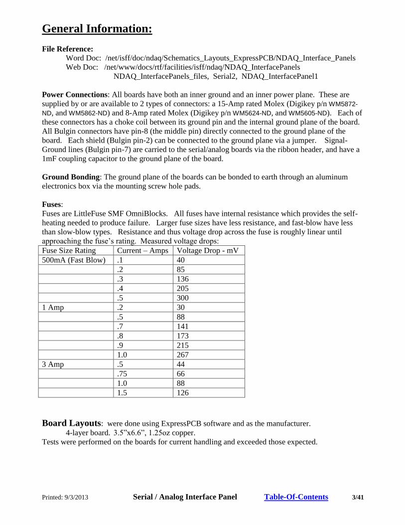
Fuses:
Fuses are LittleFuse SMF OmniBlocks. All fuses have internal resistance which provides the self-
heating needed to produce failure. Larger fuse sizes have less resistance, and fast-blow have less
than slow-blow types. Resistance and thus voltage drop across the fuse is roughly linear until
approaching the fuse’s rating. Measured voltage drops:
Fuse Size Rating Current – Amps Voltage Drop - mV
500mA (Fast Blow) .1 40
.2 85
.3 136
.4 205
.5 300
1 Amp .2 30
.5 88
.7 141
.8 173
.9 215
1.0 267
3 Amp .5 44
.75 66
1.0 88
1.5 126
Board Layouts: were done using ExpressPCB software and as the manufacturer.
4-layer board. 3.5”x6.6”, 1.25oz copper.
Tests were performed on the boards for current handling and exceeded those expected.

Printed: 9/3/2013 Serial / Analog Interface Panel Table-Of-Contents 4/41
Sensor Power / FETs:
Each Bulgin connector has 2 options to provide +Vcc to the external device. These are enabled by
use of jumper Pads JP2 (See panel layouts). This is true for all external connections on both the
Serial/Analog and Viper Interface boards:
When using the FETs, a pullup resistor is used to enable the output. The data system must turn off
the FET by pulling the lines low, floating lines will be pulled high. CHECK THESE DEFAULTS
WITH ACTUAL BOARDS/CODE! THE REDBOOT SAYS OUT0-2 COME UP AS LOGIC ‘0’
Sio Board: Diamond Emerald …
All Ports Pin-10 (Dio-X) on selected Port CHECK GM / MANUAL
Viper Board: COM1 PL9 GPIO Connector
COM1 Pin-11, OUT-0, PXA255 GPIO20 Bootup Default = OFF
COM2 Pin-18, OUT-5, PXA255 GPIO21 Bootup Default = On
COM3 Pin-20, OUT-7, PXA255 GPIO22 Bootup Default = On
COM4 Pin-16, OUT-3, PXA255 GPIO23 Bootup Default = On
COM5 Pin-14, OUT-1, PXA255 GPIO24 Bootup Default = OFF
USB Pin-15, OUT-2, PXA255 GPIO25 Bootup Default = OFF
Ethernet-1 Pin-19, OUT-6, PXA255 GPIO26 Bootup Default = On
Ethernet-2 Pin-17, OUT-4, PXA255 GPIO27 Bootup Default = On
FET Misc. Info:
IPS521G Recommended Value
Max. Continuous Current 1.6A Most sensors will be well
below this even, Li7500
High-Level, ie turn-on voltage 4.0-5.5V
Low-Level, ie. turn-off voltage -0.3-0.9V
Measured Value
Actual Turn-On Voltage 2.4V
No-Load Leakage Current
w/+5 10K pullup, ie ‘On’
.83mA @ 12.v = 10mW For one FET. This is what we
need to consider
Leakage with floating input .016mA = .1mW Ie FET ‘Off’
Leakage with +12 source
disconnected
.06mA = .7mW Ie +5 still on, but no Vcc
supply
+5V current when ‘On’ .055mA = .3mW To drive gate
3 2 1
4
4 JP2 Pin Layout
1= + Power from FET
2= Power Distribution to Bulgin
3= Vcc Plane Connection
4= FET controlled Vcc Output
Option 1: None = No Power to Bulgin Pin-1: All JP2 Jumpers Removed
Option 2: Vcc = Continuous Vcc (Battery): Jumper JP2, 2-3
Option 3: FET = FET controlled output: Jumper JP2, 3-4, 1-2

Printed: 9/3/2013 Serial / Analog Interface Panel Table-Of-Contents 5/41
Speed vs NDAQ Cable Lengths:
See the notes below about ‘NDAQ’ serial cable purchased and Ethernet issues in viper section.
Preliminary tests were performed using the SIO interface board and standard cables to observe the
signal characteristics for various data rates over both a short and longer-than-expected cable run.
Tests were done both with and without addition of an extra .01microFarad filtering capacitor on the
PCBoard. The intention of the capacitor was/is to quiet any noise and help reduce spurious resets of
the system. At lower speeds the effect of the capacitance is not critical, however at speeds above
38400bps the capacitor loads the line excessively and should not be used. This value of capacitance
adds approximately 500’ (155m) of equivalent cable length to the run. Smaller caps could be used
instead (ie .001 microFarad would add ~50’ of equivalent cable while retaining some of the filtering
capability), but this has not yet been tried.
Tests were performed using Procomm scripts on a PC running through the primary COM1 port:
RawIOloopbackTest.was Sends an alternating 1/0 character as fast as possible
and checks for loop-back receive results.
MessagePatternSendTest.was Sends a 12 char message out at nominal message
frequencies (~50hz in this case) and checks for
loopback receive results.
Specific Sensors: TRH,CSAT were also examined, powered by a power supply via the interface cable
and transmitting data into the PC.
Tests using the Viper CPU board have not been done as of June-05
The title of the images linked below indicates what the conditions were: ie ‘with-caps’ or otherwise
without; 80m cable length. NOTE because these were loopback tests, an 80m test was actually going
through 160m of cable, with 1 leg at 24.6pf and the other at 17pf per foot.
Above 38400, the PC was unable to keep up with the maximum transmit rate (ie bps) and topped out
at roughly 47kbps, due primarily to Procomm timer granularity and driver interface latency. Below
that rate everything was OK. Tests were also performed using both no flow control, soft (^s^q) and
hard (RTS,CTS) flow control. Generally the hard flow control produces less throughput.
NDAQ Cable Capacitance/Length Speed Test Images The tests roughly indicated in a lab environment: (NOTE I need to confirm these and log the data !!!!)
BPS <=20m <=20m
WithCaps
(.01mf)
80m 80m WithCaps
(.01mf)
80m
WithCaps
(.001mf)
9600 CSAT OK OK OK OK OK
9600 TRH OK OK OK OK OK
9600 OK OK OK OK OK
19200 OK OK OK OK OK
39400 OK OK OK Data OK, OK
57600 OK Data through,
lousy signal
Data through Data through,
lousy signal
Data through
115200 OK No Data through,
lousy signal
Nope: yeow! Data through,
lousy signal
Background: The following rough Rule-of-Thumb guidelines are primarily for differential signal
standards, RS422/485 with cables having 16pF/ft. capacitance. For NDAQ cables which have
slightly higher capacitance the performance should be slightly more conservative. Also, for RS232
with higher signaling levels than RS485, the effect would probably be greater, depending upon the
performance and threshold level of the transceivers used for specific devices.

Printed: 9/3/2013 Serial / Analog Interface Panel Table-Of-Contents 6/41
1) For Short-Cables (<10m): The influence of the wires can be neglected and the limiting
factor is the transceiver specifications
2) For Medium-Cables (<100m): The wire losses caused by skin effect where current is
flowing on the conductor surfaces.
3) For Long-Cables (actually all): Speed is limited by the impedance of the lines. The
Maximum impedance of the line should be less than 100ohms.
Rule-of-Thumb for Line Capacitance and Speed for RS422/485 (Differential Cabling)
Speed (Mbits/sec) * Cable-Meters <= 10^8. Ie. a 100-m cable would be able to handle
1-Mbps.
However, one Reference suggests a value roughly 1/3-times the above ‘rule’
Speed-bps 1200 56Kbps 128Kbps 256Kbps 512Kbps 1Mbps 2Mbps
Cable Length Max. 914m 488m 244m 122m 61m 30m 15m
While another Reference indicated the following far more conservative values: (Note max. length for
RS422 specification is 4000’)
Speed-bps 4800 9600 19200 38400 57600 115200
Max. Capacitance 60nf 30nf 15nf 750pf 500pf 250pf
NDAQ 24ga wire
(24.6pf/ft.)
2440’ 1214’ 310’ 30’ 20’ 10’ Simple math per
above
NDAQ 22ga wire
(17pf/ft)
3529’ 1765’ 882’ 44’ 30’ 15’ Simple math per
above
Serial Driver Output Voltage Specification Limits:
Protocol Voc Max. Spec. V-loaded Max Spec.
RS232 +/- 25 +/- 15
RS422 +/- 10 +/- 7
RS485 +/- 6 +/- 5
Standard DE-9 RS232 Pin Definitions / Signal Directions:
DTE
pin
Signal DCE - DTE (PC) DCE=Sensor/Modem
DTE=PC/Computer
1 DCD DCE announces that a connection is established
2 Rx Data received; 1 is transmitted "low", 0 as "high"
3 Tx Data sent; 1 is transmitted "low", 0 as "high"
4 DTR DTE announces that it is powered up and ready to
communicate
5 Gnd
6 DSR DCE announces that it is ready to communicate
7 RTS DTE asks DCE for permission to send data
8 CTS DCE agrees on RTS
9 RI DCE signals the DTE that an establishment of a
connection is attempted

Printed: 9/3/2013 Serial / Analog Interface Panel Table-Of-Contents 7/41
NDAQ External Cable:
Signal Line Wire Gauge Capacitance/ft. Resistance/1000-ft. A 22 17.0 pF 18.1 Ohms +12
B Shield
C 24 24.6 pF 28.7 Ohms
D 24 24.6 pF 28.7 Ohms
E 22 17.0 pF 18.1 Ohms
F 22 17.0 pF 18.1 Ohms
G 22 17.0 pF 18.1 Ohms
H 22 17.0 pF 18.1 Ohms Gnd
NDAQ cable does not meet specifications for Ethernet ‘cat5+’ (primarily the 13-17pf/foot
capacitance) and as a result works suboptimally if at all for higher distance/speed/loading. It will
work straight to the viper/interface panel at 100’. See Ethernet in viper section.
NDAQ Cable Power vs Voltage Drop: Current Rating of 22AWG used for +/- : 5A absolute max derated by .004/degC and inside jacketing.
Resistance for 22AWG copper: ~60ft/ohm at 77degF.
Thus: for 30m cable = 3.28 ohms … 30*3.28(ft/m) = 98 * 2 (goes up/down) = 196/60 = 3.28
so for a ~1.2A load and 12.2Vin - 3.8 (IRloss) ~=8.4Volts at licor sensor for example.
Bulgin Pin Assignments:
E,F,G
Shielded
24-Awg
with Drain
Shielded
22-Awg with
Drain
Unshielded
22-Awg
Cable Bulgin Color Nom.Sig. A
A 1 Red +12
B 2 Bare Shield
C 5 White
D 4 Black
E 3 Brown
F 6 Orange
G 7 Yellow SigGnd
H 8 Black Ground
A
H
B C,D

Printed: 9/3/2013 Serial / Analog Interface Panel Table-Of-Contents 8/41
Serial / Analog Panel: Emerald DMM-8 Board Layout / Jumpers

Printed: 9/3/2013 Serial / Analog Interface Panel Table-Of-Contents 9/41
Sensor Specific Wiring:
CSAT-3 Sonic Note: the CSAT electronics box was modified to bring power out to the CSAT comm./serial
connector to avoid using a second connection: the ‘factory’ power connector.
CSAT-3
Signal
CSAT-3
Connector Pin
Bulgin
Pin
Cable-Wire ‘GreenJacket’
Cable-Wire ‘Thick-
Gray (tape color)’
Transmit Data from
CSAT to PC B 5
C = White,
with… White
RTS G 4 D = Black Purple
CTS H 3 E = Brown Brown
Receive Commands
from PC C 6 F = Orange Orange
Ground E 7 G = Yellow Yellow
+12 VDC D 1 A = Red Red
Ground F 8 H = Black Gray
2 B – no connect -
Garmin GPS 4800bps for standard NMEA messages.
GPS
Signal
Bulgin
Pin
Garmin Cable-Wire
Color +12 VDC 1 Red
Shield 2 Bare Shield
1-PPS signal 3 Gray
4 n/c
Transmit Data-1 from
GPS to PC 5 White
Receive Commands-1
from PC 6 Blue
7 n/c
Ground 8 Black
MaxStream XBee / Xtend Radio Modems The maxstream will work on the generic sio interface or the Viper ports, per note ‘dtr’ below. DE-9
Male-
pins
Signal (Max) DCE -
DTE (Viper)
Bulgin
Pin
DCE=Sensor/Modem
DTE=PC/Computer
1 DCD n/c
2 Rx 5 Radio Output to Viper
3 Tx 6 Radio Receive from Viper
4 DTR 7 Used to Enable Power Down Mode on Radio.
Note: DTR is only available on Viper ports COM1 and
COM4. On SioPanels, DTR is on Bulgin pin-3 and
must be selected by jumper.
5 Gnd 8
6 DSR n/c
7 RTS 4 RTS Flow Control, or enter Command Mode of Radio
8 CTS 3 CTS Flow Control,
9 RI 1 Used for POWER in our application

Printed: 9/3/2013 Serial / Analog Interface Panel Table-Of-Contents 10/41
Niwot08 TelosB PAR-Mote-Box, Tsoil-Mote-Box, Mote-Repeater-Box MiniDin
pins
Signal (Max) DCE -
DTE (Viper)
Bulgin
Pin
DCE=Sensor/Modem
DTE=PC/Computer
1 Rx 5 TelosB Output to Adam
2 Tx 6 TelosB Input from Adam
3,5 +12
VDC 1
4 Gnd 8
6 Reset 4 RTS, Remove Jumper J9 on Mote-Board to Disable
RMY 9101 PropVane Anemometer
The sensor has only Serial RS485 or analog speed/direction output. They were programmed to
conform to the NCAR – SBUS protocol. For NDAQ, primary use is expected to be with the 1-
second continuous data output option; otherwise a polling mechanism for SBUS messages is
needed….#12ODf<EOT> where the ‘f’ is a checksum equivalent, EOT=0x04 and 12 = RMYaddr
Signal RMY 9101 Pin Wire
Color
Bulgin
Pin
Cable-Wire Cable-Wire Color ‘GreenJacket’
RS485- B Blk 4 D Black, bundled with…
RS485+ A Wht 5 C White
Sig-Gnd Ref (common) Yel 7 G Yellow, bundled with…
3,6 E,F – no connect Brown, Orange
+12 VDC Pwr Red 1 A Red, non-shielded
Ground Earth (common) Blk 8 H Black, non-shielded
2 B Bare Shield
PORT Connection: ttyS4, Viper Panel COM-5 can be used for the Prop-Vane.
Important: Make sure Viper board LK6-7 are in the RS485 position as noted in the ViperCPU photo
RMY9101 Manual.pdf RMY9101 Old-PAM Notes.pdf
NCAR TRH Note: Internal Jumpers
The sensor is capable of either RS232 or RS485, however both a jumper wire and a jumper header
must be set up to select between these two options inside the TRH.
For RS232: J3-1 blue wire to Bulgin-4; Jumper header J5: 2-3 (toward sensor end of board)
For RS485: J1-1 white wire to Bulgin-4; Jumper header J5: 1-2 (toward connector end of board)
Note: Sensor Setup
The TRH is capable of either ‘SBUS’ or ‘Interactive’ operation. With NIDS/NDAQ there is no sbus
interaction software. There are 2 ways to enter interactive mode:
1) ‘esc-esc-esc’ while communicating with an sbus device
2) change the default operation. To setup default interactive mode establish a session on EVE most
likely with EVE or else use the sequence in 1 above; then use the following basic command sequence
after getting into ‘PH’ help:
‘EE’ enter eeprom submenu
‘protocol=1’ turns off sbus, on interactive mode (‘=0’ is sbus)
‘mode=1’ turns on auto output mode (‘=0’ is polled)
‘EE’ exit eeprom submenu

Printed: 9/3/2013 Serial / Analog Interface Panel Table-Of-Contents 11/41
‘MR’ reset
TRH Quick Reference
Signal TRH Berg Pin Wire
Color
Bulgin
Pin
Cable-Wire Cable-Wire Color ‘GreenJacket’
RS485+ J1-1, jmp select Wht 5 C White, bundled with
RS232 – Tx Data
from TRH to PC J3-1, jmp select
Blue 5
C White, bundled with
RS485- J1-2 4 D Black
RS232 – Rx
Cmds from PC J3-2
6
F Orange, bundled with…
2,3 B,E - no connect Bare, Brown
SigGnd J3-3, intern short
with
7
G Yellow
Shield J1-3 7 G
+12 VDC J2-1 Red 1 A Red, non-shielded
Ground J2-2 Blk 8 H Black, non-shielded

Printed: 9/3/2013 Serial / Analog Interface Panel Table-Of-Contents 12/41
Generic Serial Wiring:
Power Options Option Jumpering FET Status FET Control
Vcc JP2: 2-3 FET disabled (JP4 Out) n/a
FET JP2: 1-2, 3-4 FET enabled (JP4 In) DIO-x (for portx)
emerald_dio /dev/ttyD5 0,1
None JP2: all removed FET disabled (JP4 Out) n/a
TVS Use / Shielding Option TVS Array Used Shielded Pair 4,5 – C,D Shielded Triad 3,6,7 –E,F,G RS232 VS10P15LC Rx/RTS Tx/CTS/SigGnd
RS422 VS10P08LC Tx+/Tx- Rx+/Rx-/SigGnd
RS485 VS10P08LC Tx+/-, Rx+/- SigGnd
RS232 Cable-Wire Bulgin Ribbon-10 to PC104 line Protection / Interface A = Red 1 (Power +Vcc) TVS SMC, RLC Choke/Filter -Gnd
B = Bare 2 (Shield) Jumper to Ground Plane
H = Black 8 (Ground) Direct connect to Ground Plane
1 = DCD, 2=DSR, 8=RI (n/c)
C = White 5 3 = Rx (Input data to PC) TVS array, .01mF Filter Cap.-Gnd
D = Black 4 4 = RTS TVS array, .01mF Filter Cap.-Gnd
F = Orange 6 5 = Tx (Jmp-3 Select `232’) TVS array, .01mF Filter Cap.-Gnd
E = Brown 3 6 = CTS TVS array, .01mF Filter Cap.-Gnd
7 = DTR (n/c Jmp-3 De-select)
G = Yellow 7 (SigGnd) 9 = Gnd 1mF Filter Cap.-Gnd
10 = DIO (FET power ctrl)
RS422 Cable-Wire Bulgin Ribbon-10 to PC104 line Protection / Interface A = Red 1 (Power +Vcc) TVS SMC, RLC Choke/Filter -Gnd
B = Bare 2 (Shield) Jumper to Ground Plane
H = Black 8 (Ground) Direct connect to Ground Plane
1,2,8 = (n/c)
C = White 5 3 = Tx+ TVS array, .01mF Filter Cap.-Gnd
D = Black 4 4 = Tx- TVS array, .01mF Filter Cap.-Gnd
5 = Gnd (n/c Jmp-3 De-select)
E = Brown 3 6 = Rx- TVS array, .01mF Filter Cap.-Gnd
F = Orange 6 7 = Rx+ (Jmp-3 Select ‘422’) TVS array, .01mF Filter Cap.-Gnd
G = Yellow 7 (SigGnd) 9 = Gnd 1mF Filter Cap.-Gnd
10 = DIO (FET power ctrl)
RS485 Cable-Wire Bulgin Ribbon-10 to PC104 line Protection / Interface A = Red 1 (Power +Vcc) TVS SMC, RLC Choke/Filter -Gnd
B = Bare 2 (Shield) Jumper to Ground Plane
H = Black 8 (Ground) Direct connect to Ground Plane
1,2,8 = (n/c)
C = White 5 3 = Tx+ / Rx+ TVS array, .01mF Filter Cap.-Gnd
D = Black 4 4 = Tx- / Rx- TVS array, .01mF Filter Cap.-Gnd
5 = Gnd (n/c Jmp-3 Removed)
E = Brown 3 (Available) 6 = (n/c) TVS array, .01mF Filter Cap.-Gnd
F = Orange 6 (Available via jumper) 7 = (n/c) (Jmp-3 Removed) TVS array, .01mF Filter Cap.-Gnd
G = Yellow 7 (SigGnd) 9 = Gnd .01mF Filter Cap.-Gnd
10 = DIO (FET power ctrl)

Printed: 9/3/2013 Serial / Analog Interface Panel Table-Of-Contents 13/41
SIO Interface Panel – Component Current / Power Capacity:
Current capacity of the board is dictated by various components on it and the power distribution from
the main ‘dc-dc’ panel.
It is also dependent upon overall board and component temperature. In general current capacity goes
down with temperature for lans/wire, but improves for components that are limited on internal
junction temp/heat sinking.
Component Rating Comment
Bulgin Pins 5A Max for Pins/Sockets (p/n 3347 and 3348)
22AWG Wire for +/-
to Sensors
5A Absolute max derated by .004degC and inside jacketing
AWG Wire for +/- to
board from Power
Panel
Board Connectors 15A 5mm Black 2-pin Molex (wm5872-nd, wm5862-nd)
8A 3.5mm Black 2-pin Molex (wm5624-nd, wm5605-nd)
PCB Total 8A ? Measured once at room temp but should redo at cold
(lower capacity). Board has internal power/ground
planes, so ‘really big lan’.
Board LANs ~0.7A@-10degC
~1.5A@0degC
~2.0A@10degC
~4.0A@45degC
.080” x 1.25 Oz./ft^2 copper trace through coil, fuse to
Bulgin connector. Tested to much more temporarily at
room temp.
FET 1.4A @ 125degF
2.0A @ 75degF
2.6A @ 25degF
10A peak
IRL IPS521G part. Max continuous current is dictated
by Junction Temperatures. These improve with lower
ambient temps. and better heat sinking on chip or lan.
The NDAQ board was not designed with any special heat
sinking capabilities.
Coil, power choke. 3.4A @ 45degC Panasonic (pcd1362ct-nd). Dependant on part temp.
Pin on +12 Distrib. 3A Sullens .1” breakaway (s1011-35-nd)
Shunts on PowerPin 3A Sullens .1” (s9000-nd)
DC-DC converter 1.8A For providing +15VDC to board, used for Ethernet on
viper in particular. (20W module)

Printed: 9/3/2013 Serial / Analog Interface Panel Table-Of-Contents 14/41
PCBoard:

9/3/2013 Serial / Analog Interface Panel Table-Of-Contents 15/41
Layout:
Jumper JP1 to connect
Shield to Ground Jumper JP3 to select
RS232-Tx vx RS422-
Rx+
Jumper JP5 to Turn on +5 Jumper JP4 For +5V
Pullup FET Input gate
Jumper JP2 for Power Output Option
Select and Vcc to FET

9/3/2013 Serial / Analog Interface Panel Table-Of-Contents 16/41
Schematic:

9/3/2013 VIPER CPU Interface Panel - Table-Of-Contents 17/41
VIPER CPU Panel:
Arcom VIPER Board Layout / Jumpers
LK6,7 Position for
COM5 RS485 ..toward
the flash-card drive

9/3/2013 VIPER CPU Interface Panel - Table-Of-Contents 18/41
Device Specific Wiring:
System Console to PC Note: This is a ‘null modem’ for PC to Viper, COM1 = /dev/ttyS0.
The same wiring would work on the other ports as well, however, to connect a true DCE such as a
sensor you need to swap 5-6 (Tx/Rx) and 3-4 (RTS/CTS) and the Viper becomes the DTE.
DE-9
pin
Signal (Viper) DCE -
DTE (PC)
Bulgin
Pin
DCE=Sensor/Modem
DTE=PC/Computer
1 DCD n/c
2 Rx 6
3 Tx 5
4 DTR 7 Note: DTR is only available on Viper ports COM1 and
COM4. Don’t connect this on other ports because
pin-7 is used for siggnd which could harm PC
5 Gnd 8
6 DSR n/c
7 RTS 3
8 CTS 4
Terabeam EtherAntIII-LR Note: This is an ethernet Cross-Over cable for the Viper, Eth1 port
Cable-Wire ‘GreenJacket’
Bulgin
EantIII
(xover)
Bulgin
TPOP
(straight)
Signal Switchcraft
Connector
(SC1163-ND)
(EtherAnt)
Protection / Interface
A = Red 1 1 Power +Vcc 5
B = Bare 2 2 Shield Jumper to Ground Plane
C = White 3 5 Tx+ 1 (has dot)
D = Black 6 4 Tx- 2
F = Orange 4 6 Rx - 4
E = Brown 5 3 Rx+ 3
G = Yellow 7 7 Optional
LANGnd
H = Black 8 8 Ground 6 Connection to Ground Plane
Signal Engineering SE12xx GOES Transmitter Note: This works for Viper COM4, or the generic Emerald RS232 panel. RTS/CTS are required.
DCD/DTR/DSR/RI not needed.
Note: For ADAM-Box Internal Wiring use ‘FrontPanel-Ribbon10’ to ‘Goes Ribbon14 or 10’. Signal (Viper) DCE - DTE
(PC)
Bulgin
Pin
Front Panel: Viper/
Emerald
Ribbon-10
Ribbon-14,
SE120 or
SE1200
Ribbon-10
OmniSat
Rx From GOES to PC
‘Viper/Diamond’
5 3 14 3
Tx To GOES from PC 6 5 (via JP3) 13 5
Gnd 8 9 2,4,6 9,10
RTS To GOES from PC 4 4 11 4
CTS From GOES to PC 3 6 12 6
9/3/2013 VIPER CPU Interface Panel - Table-Of-Contents 19/41
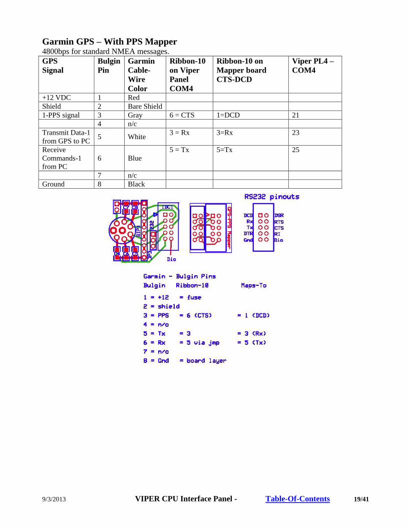
Garmin GPS – With PPS Mapper 4800bps for standard NMEA messages.
GPS
Signal
Bulgin
Pin
Garmin
Cable-
Wire
Color
Ribbon-10
on Viper
Panel
COM4
Ribbon-10 on
Mapper board
CTS-DCD
Viper PL4 –
COM4
+12 VDC 1 Red
Shield 2 Bare Shield
1-PPS signal 3 Gray 6 = CTS 1=DCD 21
4 n/c
Transmit Data-1
from GPS to PC 5 White
3 = Rx 3=Rx 23
Receive
Commands-1
from PC
6 Blue
5 = Tx 5=Tx 25
7 n/c
Ground 8 Black

9/3/2013 VIPER CPU Interface Panel - Table-Of-Contents 20/41
Viper DIO Interface Mapper

9/3/2013 VIPER CPU Interface Panel - Table-Of-Contents 21/41
Viper COM-Ports: The Viper has 5 COM ports available on a 40-pin , .1” IDC header named
PL4. These are split out into 4 individual 10-pin receptacles for distribution to the interface board
headers.
COM-1:
Console: RTS/CTS/DTR; /dev/ttyS0
TVS Array FET Power Control Shielded Pair
4,5 – C,D Shielded Triad
3,6,7 –E,F,G PLCDA15C-6 OUT-0 (Viper PL9-11) Rx/RTS Tx/CTS/DTR
Notes: SigGnd wire ‘stolen’ to provide protection for DTR on Bulgin pin-7
Cable-Wire ‘GreenJacket’
Bulgin Ribbon-10 Viper
PL4
Protection / Interface
A = Red 1 (Power +Vcc) TVS SMC, RLC Choke/Filter -Gnd
B = Bare 2 (Shield) Jumper to Ground Plane
1 = DCD (n/c) 31
2 = DSR (n/c) 32
C = White 5 3 = Rx 33 TVS array, .01mF Filter Cap.-Gnd
D = Black 4 4 = RTS 34 TVS array, .01mF Filter Cap.-Gnd
F = Orange 6 5 = Tx 35 TVS array, .01mF Filter Cap.-Gnd
E = Brown 3 6 = CTS 36 TVS array, .01mF Filter Cap.-Gnd
G = Yellow 7 7 = DTR 37 TVS array, .01mF Filter Cap.-Gnd
8 = RI (n/c) 38
H = Black 8 (Ground) 9 = Gnd 39 Direct connection to Ground Plane
10 = (n/c) 40
COM-2:
RTS/CTS; /dev/ttyS1
TVS Array FET Power Control Shielded Pair
4,5 – C,D Shielded Triad
3,6,7 –E,F,G VS10P15LC OUT-5 (Viper PL9-18) Rx/RTS Tx/CTS/SigGnd
Cable-Wire ‘GreenJacket’
Bulgin Ribbon-10 Viper
PL4
Protection / Interface
A = Red 1 (Power +Vcc) TVS SMC, RLC Choke/Filter -Gnd
B = Bare 2 (Shield) Jumper to Ground Plane
H = Black 8 (Ground) Direct connection to Ground Plane
1 = Tx3 11
2 = Rx3 12
C = White 5 3 = Rx2 13 TVS array, .01mF Filter Cap.-Gnd
D = Black 4 4 = RTS2 14 TVS array, .01mF Filter Cap.-Gnd
F = Orange 6 5 = Tx2 15 TVS array, .01mF Filter Cap.-Gnd
E = Brown 3 6 = CTS2 16 TVS array, .01mF Filter Cap.-Gnd
7 = Gnd 17
8 = Gnd (n/c) 18
G = Yellow 7 (SigGnd) 9 = Gnd 19 .01mF Filter Cap.-Gnd
10 = (n/c) 20

9/3/2013 VIPER CPU Interface Panel - Table-Of-Contents 22/41
COM-3:
Tx/Rx Only; /dev/ttyS2
TVS Array FET Power Control Shielded Pair
4,5 – C,D Shielded Triad
3,6,7 –E,F,G VS10P15LC OUT-7 (Viper PL9-20) Rx Tx/SigGnd
Cable-Wire ‘GreenJacket’
Bulgin Ribbon-10 (with COM2)
Viper
PL4
Protection / Interface
A = Red 1 (Power +Vcc) TVS SMC, RLC Choke/Filter -Gnd
B = Bare 2 (Shield) Jumper to Ground Plane
H = Black 8 (Ground) Direct connection to Ground Plane
F = Orange 6 1 = Tx3 11 TVS array, .01mF Filter Cap.-Gnd
C = White 5 2 = Rx3 12 TVS array, .01mF Filter Cap.-Gnd
3 = Rx2 13
D = Black 4 (n/c) 4 = RTS2 14
5 = Tx2 15
E = Brown 3 (n/c) 6 = CTS2 16
G = Yellow 7 (SigGnd) 7 = Gnd 17 .01mF Filter Cap.-Gnd
8 = Gnd (n/c) 18
9 = Gnd 19
10 = (n/c) 20
COM-4:
RTS/CTS/DTR; /dev/ttyS3
TVS Array FET Power Control Shielded Pair
4,5 – C,D Shielded Triad
3,6,7 –E,F,G PLCDA15C-6 OUT-3 (Viper PL9-16) Rx/RTS Tx/CTS/DTR
Notes: SigGnd wire ‘stolen’ to provide protection for DTR on Bulgin pin-7
Cable-Wire ‘GreenJacket’
Bulgin Ribbon-10 Viper
PL4
Protection / Interface
A = Red 1 (Power +Vcc) TVS SMC, RLC Choke/Filter -Gnd
B = Bare 2 (Shield) Jumper to Ground Plane
1 = DCD (n/c) 21
2 = DSR (n/c) 22
C = White 5 3 = Rx 23 TVS array, .01mF Filter Cap.-Gnd
D = Black 4 4 = RTS 24 TVS array, .01mF Filter Cap.-Gnd
F = Orange 6 5 = Tx 25 TVS array, .01mF Filter Cap.-Gnd
E = Brown 3 6 = CTS 26 TVS array, .01mF Filter Cap.-Gnd
G = Yellow 7 7 = DTR 27 TVS array, .01mF Filter Cap.-Gnd
8 = RI (n/c) 28
H = Black 8 (Ground) 9 = Gnd 29 Direct connection to Ground Plane
10 = (n/c) 30
COM-5:
RS485 (half-duplex) /422; /dev/ttyS4

9/3/2013 VIPER CPU Interface Panel - Table-Of-Contents 23/41
Note: DC-DC Auxiliary Power
An additional Sensor Power Option is available via CON5 intended to feed to and back from a
separate DC-DC converter.
Note that because of this, 2 jumpers are needed to provide power to the external device/s
Note: Viper Setup for Half-Duplex RS485
Viper Jumper selections: LK6,LK7 to position A=RS485, to position B=RS422 (see figure above or
technical manual)
Note: See TRH Setup Above for Interactive Mode / RS485. See RMY9101 for more about wiring.
TVS Array FET Power Control Shielded Pair
4,5 – C,D Shielded Triad
3,6,7 –E,F,G VS10P08LC OUT-1 (Viper PL9-14) Tx+/- (RS422)
Tx+/-,Rx+/- (RS485)
Rx+/-,SigGnd (RS422)
SigGnd (RS485
Sensor Power
Option
Jumpering
Vcc CON5: 1-2
JP2: 2-3 FET disabled JP4 Out
FET CON5: 1-2
JP2: 1-2, 3-4
JP2: 1-2
FET enabled JP4 In
+15SubModule JP2: 2-3 FET disabled JP4 Out
None JP2: all removed FET disabled JP4 Out
Cable-Wire ‘GreenJacket’
Bulgin Ribbon-10 Viper
PL4
Protection / Interface
A = Red 1 (Power +Vcc) TVS SMC, RLC Choke/Filter -Gnd
B = Bare 2 (Shield) JP1, Jumper to Ground Plane
H = Black 8 (Ground) Direct connection to Ground Plane
1 = n/c 1
2 = n/c 2
3 = n/c 3 TVS array, .01mF Filter Cap.-Gnd
4 = n/c 4 TVS array, .01mF Filter Cap.-Gnd
C = White 5 5 = Tx+ (422)
Tx+/Rx+ (485)
5 TVS array, .01mF Filter Cap.-Gnd
D = Black 4 6 = Tx- (422)
Tx-/Rx- (485)
6 TVS array, .01mF Filter Cap.-Gnd
F = Orange 6 7 = Rx+ (422) 7
E = Brown 3 8 = Rx- (422) 8
G = Yellow 7 (SigGnd) 9 = Gnd 9 C4 - 1mF Filter Cap.-Ground Plane
10 = Gnd 10

9/3/2013 VIPER CPU Interface Panel - Table-Of-Contents 24/41
USB Errata:
Operating Speeds:
Low Speed = 1.5 Mbps (can use non-shielded cable)
Full Speed = 12 Mbps (USB1.1, requires shielded cable)
High Speed = 480 Mbps (USB2.0 and above)
This includes overhead so actual rates will be slightly lower.
Speed Identification
Devices identify to a host whether they are slow or full by pulling one of the data lines.
These are also used by the host to identify when a device is connected.
Full speed: pulls up D+ to 3.3
Some devices use programmable pull-ups so that they can initialize themselves before
notifying the host of their presence.
Electrical
Differential Data transmission, NRZ1 with bit stuffing
Low/full speed devices: 1 has D+=>2.8V, D-=<.3V; 0 has D+=<.3V,D-=>2.8
Receiver needs differential ‘1’ as D+ 200mV>D- and vis-versa
Signal polarity reversed based on speed of bus: ‘J’=logic levels and for low speed ‘J’is
differential 0, in high speed ‘J’ is a differential 1
Power: +5V operation
Pin Desc.
1 = Vbus (+5)
2 = D-
3 = D+
4 = Gnd
Type-A Connector
Located on Host/Hub
Type-B Connector
Located on Device (Slave)
Low Speed Devices have a
pull-up resistor on D- to
identify themselves to a host
High Speed Devices have a
pull-up resistor on D+ to
identify themselves to a host.
USB-2 = 480Mbits/sec

9/3/2013 VIPER CPU Interface Panel - Table-Of-Contents 25/41
System Configuring: All devices include internal information specifying various
parameters including the amount of power they’ll consume from the bus.
Voltage, operating = 4.75 – 5.25V
Max. voltage drop = 0.35
Min. config voltage = 4.4 (min. voltage to send config. On bus but other functions
don’t need to be operating at that low a value)
Low, Bus Powered functions 100mA max. (1-unit load) for between 4.4-5.25V, device
draws all power from bus.
High, Bus Powered functions 100mA max at startup, 500mA max. After
startup/configure period, it may draw up to 500mA, or less depending upon what it
declares in it’s descriptor.
Self Powered functions 100mA max., device draws all remaining power internally.
Suspend Mode .5mA max. Note, implementation is complicated by the
pull-up identifying resistors in the design.
Cabling / Lengths:
Shielding: should only be connected to ground at Host! No device should do it.
Shielded Cable: 28AWG twisted
Power: 20-28AWG non-twisted
Max. Length: 28 = .8m
26 = 1.3m
24 = 2.1m
22 = 3.3m
20 = 5m
Decoupling Capacitance: 1microF recommended between Vbus-Gnd in a device. This relates
to limited specification of in-rush current. The maximum for a device is 10microF.
USB-OTG: On-The-Go
Supplement to the Specification released Dec-2001.
Introduces idea of devices being allowed to be sometimes a host or slave in order to
permit connectivity without the need for a main PC host. Example: digital
cameras talking directly to a printer
Connectors added: Mini-A, Mini-B, and Mini-AB (for dual-role devices)
Wireless USB-OTG: big emerging market
2.4Ghz, DSSS, much less complex than Blue-Tooth or Zigbee
Not a multi-tiered net, small packet data, doesn’t require periodic net sync.
Cable replacement, up to 62.5kbps
10-50m
Cypress Semiconductor developed this capability and offers starter devel. Kits.,
SPI intf. to micro
USB-1, USB-2 Cabling: The Viper has 2 USB ports. Both are routed to the interface panel but only 1, USB-2 is taken to the
outside via the Bulgin connector. This decision allowed the power supply circuit to still be available
on the Bulgin connector rather than having both USB’s on it instead.

9/3/2013 VIPER CPU Interface Panel - Table-Of-Contents 26/41
TVS Array FET Power Control Shielded Pair
4,5 – C,D Shielded Triad
3,6,7 –E,F,G SRV05-4 OUT-2 (Viper PL9-15) DNEG-2/DPOS2 VBUS2/Gnd
Notes:
Cable-
Wire
Bulgin Ribbon-10 -
Viper PL7
Protection / Interface On-Board USB
Type-A Conn. A = Red 1 (Power, +Vcc) F1, TVS SMC, RLC Choke/Filter -
Gnd
1 = VBUS-1 TVS/Diode array1, 1mF Cap.-Gnd USB-1, Pin-1
E = 3 2 = VBUS-2 TVS/Diode array2, 1mF Cap.-Gnd USB-2, Pin-1
3 = DNEG-1 TVS/Diode array-1 USB-1, Pin-2
C = 5 4 = DNEG-2 TVS/Diode array-2 USB-2, Pin-2
5 = DPOS-1 TVS/Diode array-1 USB-1, Pin-3
D = 4 6 = DPOS-2 TVS/Diode array-2 USB-2, Pin-3
H = Black 8 Ground Plane 7 = Gnd C4 - 1mF Filter Cap.-Gnd Plane USB-1, Pin-4
G = 7 8 = Gnd C4 - 1mF Filter Cap.-Gnd Plane USB-2, Pin-4
F = 6 (n/c) 9 = Shield
B = Bare 2 (Shield jump to ribbon) 10 = Shield
Ethernet Cabling: Twisted-pair Ethernet (10BASE-T, 100BASE-T, or 1000BASE-T) uses an
RJ-45 connector, which is an eight-pin modular connector
CrossOver: Two Ethernet stations can be directly attached to each Other but the cabling will be wired differently than a normal 10BASE-T
Ethernet network connection. The 802.3 specification refers to this
direct connection between two stations as a crossover function.
The crossover function is accomplished by simply wiring the receive
pins to the transmit pins as shown above.
CAT6 essentially obsoletes the CAT5 standard and will obsolete the CAT5e standard. CAT6 was
introduced with the publication of the TIA standard 568-B2-1 (June 20, 2002). The bandwidth is
more than doubled from 100MHz to 250MHz and the connector insertion loss and the crosstalk is
improved.
CAT 5: 4 Twisted Pairs at 24 AWG
Cross-Over Cable 1 = Tx+
2 = Tx-
3 = Rx+
4 = (n/c)
5 = (n/c)
6 = Rx-
7 = (n/c)
8 = (n/c)

9/3/2013 VIPER CPU Interface Panel - Table-Of-Contents 27/41
pair 1: blue
pair: 2 orange
pair: 3 green
pair: 4 brown
(twisted about 3 times per inch)
Straight Ethernet Cable
Cross-Cable
Ethernet uses only pair 3 (green, on pins 1 and 2), and pair 2 (orange, on pins 3 and 6).
EIA/TIA specifies RJ-45 (ISO 8877) connectors for UTP cable (unshielded twisted pair).
Impedance: 100 Ohms
Max length of a segment: 100 meters/330 feet
Frequency rating: 100MHz
Capacitance 13.5 to 17 picofarads per foot
Attenuation 23 to 67dB per 1000 feet
Crosstalk 32 to 51 dB at 1000 feet
CAT 5 Cable Specifications:
Frequency Max.
Attenuation
per 1000 ft/
304 m
Resistance
per 1000 ft/
304 m
Capacitance Impedance
4 MHz 13 dB 28,6 ohms 14 pF/ft 100 ohms
10 MHz 20 dB 28,6 ohms 14 pF/ft 100 ohms
20 MHz 28 dB 28,6 ohms 14 pF/ft 100 ohms
100 MHz 67 dB 28,6 ohms 14 pF/ft 100 ohms

9/3/2013 VIPER CPU Interface Panel - Table-Of-Contents 28/41
CAT 3, 4, 5, 5e, 6, 7 Cable Specifications:
Category Type Spectral
B/W Length
LAN
Applications Notes
Cat3 UTP 16 MHz 100m 10Base-T, 4Mbps Telephone
Cables
Cat4 UTP 20 MHz 100m 16Mbps Rarely Used
Cat5 UTP 100MHz 100m 100Base-
Tx,ATM, CDDI LAN
Cat5e UTP 100MHz 100m 100Base-T LAN
Cat6 UTP 250MHz 100m 1000Base-T LAN
Cat7 ScTP 600MHz 100m 1000Base-T LAN
CAT 5, 5e, 6 Detailed Cable Specifications:
CAT 5 CAT 5e CAT 6
Frequency 100 MHz 100 MHz 250 MHz
Attenuation (Min. at 100 MHz) 22 dB 22 dB 19.8 dB
Characteristic Impedance 100 ohms
± 15%
100 ohms
± 15%
100 ohms
± 15%
NEXT (Min. at 100 MHz) 32.3 dB 35.3 dB 44.3 dB
Return Loss (Min. at 100 MHz) 16.0 dB 20.1 dB 20.1 dB
Cat5 Wiring Standards, Listed
Pin EIA/TIA
568A
AT&T
258A,
EIA/TIA
568B
10Base-
T
10Mbps
Cat3
100Base-
TX
100Mbps
Cat5
100Base-
T4
100Mbps
Cat3
100Base-
T2
100Mbps
Cat3
1000Base-
T
1Gbps
Cat5+
1 white/green white/orange TX+ TX+ TX D1+ BI DA+ BI DA+
2 green/white orange/white TX- TX- TX D1- BI DA- BI DA-
3 white/orange white/green RX+ RX+ RX D2+ BI DB+ BI DB+
4 blue/white blue/white na na BI D3+ na BI DC+
5 white/blue white/blue na na BI D3- na BI DC-
6 orange/white green/white RX- RX- RX D2- BI DB- BI DB-
7 white/brown white/brown na na BI D4+ na BI DD+
8 brown/white brown/white na na BI D4- na BI DD-
BI=BI directional data RX=Receive Data TX=Transmit Data

9/3/2013 VIPER CPU Interface Panel - Table-Of-Contents 29/41
10BaseT and 100BaseT Cross Cable
Pin Color Code Color Code Pin
1 White/Orange White/Green 1
2 Orange Green 2
3 White/Green White/Orange 3
4 Blue Blue 4
5 White/Blue White/Blue 5
6 Green Orange 6
7 White/Brown White/Brown 7
8 Brown Brown 8
Ethernet-1
Note: An additional Sensor Power Option is available via CON5 intended to feed to and back from a
separate DC-DC converter.
TVS Array FET Power Control Shielded Pair
4,5 – C,D Shielded Triad 3,6,7 –
E,F,G SRV05-4 OUT-6 (Viper PL9-19) Tx+/- Rx+/-,LANGnd
Sensor Power
Option
Jumpering
Vcc CON5: 1-2
JP2: 2-3 FET disabled JP4 Out
FET CON5: 1-2
JP2: 1-2, 3-4
JP2: 1-2
FET enabled JP4 In
+15SubModule JP2: 2-3 FET disabled JP4 Out
None JP2: all removed FET disabled JP4 Out
Cable-Wire ‘GreenJacket’
Bulgin to External Ribbon-8 -
Viper PL1
Protection / Interface On-Board Eth.
Modular Jack A = Red
1 (Power +Vcc) F1, TVS SMC, RLC Choke/Filter -
Gnd
B = Bare 2 (Shield: jumper to gnd) JP1, Thermal Pad to Ground Plane
H = Black 8 Ground Plane Thermal Pad to Ground Plane
C = White 5 1 = Tx+ TVS/Diode array1 ETH1, Pin-1
D = Black 4 2 = Tx- TVS/Diode array2 ETH1, Pin-2
E = Brown 3 3 = Rx+ TVS/Diode array-1 ETH1, Pin-3
4 = RJ-2
5 = RJ-2
F = Orange 6 6 = Rx- TVS/Diode array-2 ETH1, Pin-6
G = Yellow 7 (JP6 jump to Gnd) 8 = LANGnd

9/3/2013 VIPER CPU Interface Panel - Table-Of-Contents 30/41
Ethernet-2
TVS Array FET Power Control Shielded Pair
4,5 – C,D Shielded Triad 3,6,7
–E,F,G SRV05-4 OUT-4 (Viper PL9-17) Tx+/- Rx+/-
Cable-
Wire
Bulgin to External Ribbon-8 -
Viper PL1
Protection / Interface On-Board Eth.
Modular Jack A = Red 1 (Power +Vcc) F1, TVS SMC, RLC Choke/Filter -Gnd
B = Bare 2 (Shield: jumper to gnd) JP1, Thermal Pad to Ground Plane
H = Black 8 Ground Plane Thermal Pad to Ground Plane
C = 5 TVS/Diode array1 ETH2, Pin-1
D = 4 TVS/Diode array2 ETH2, Pin-2
E = 3 TVS/Diode array-1 ETH2, Pin-3
F = 6 TVS/Diode array-2 ETH2, Pin-6
G = 7 (n/c)

9/3/2013 VIPER CPU Interface Panel - Table-Of-Contents 31/41
Layout:
Jumper JP5 to Turn on
+5
Jumper JP1 to connect
Shield to Ground
Jumper JP2 for Power Output Option
Select and Vcc to FET Jumper JP4 For +5V
Pullup FET Input gate

9/3/2013 VIPER CPU Interface Panel - Table-Of-Contents 32/41

9/3/2013 VIPER CPU Interface Panel - Table-Of-Contents 33/41
Schematic:

9/3/2013 VIPER CPU Interface Panel - Table-Of-Contents 34/41

9/3/2013 VIPER CPU Interface Panel - Table-Of-Contents 35/41

9/3/2013 Power Distribution Panel Table-Of-Contents 36/41
Power Distribution Panel:
Description: This board was laid out for interfacing the NDAQ to the external station power
cabling using AMP 4-pin CPC series connectors. These were selected to be compatible with existing
PAM-III cabling.
4-layer board. 3.5”x4.0”
1.25oz copper
ExpressPCB layout and manuf.
Nominal Current Capacity for various trace sizes. The table below gives rough guidelines of how
wide to make a trace for a given amount of current. Elevated temperatures reduce trace capacity.
0.010" 0.3 Amps
0.015" 0.4 Amps
0.020" 0.7 Amps
0.025" 1.0 Amps
0.050" 2.0 Amps
0.100" 4.0 Amps
0.150" 6.0 Amps
When placing a trace, it is very important to think about the space between the trace and any adjacent
traces or pads. You want to make sure that there is a minimum gap of 0.007" between items, 0.010" is
better. Leaving less blank space runs the risk of a short developing in the board manufacturing
process. It is also necessary to leave larger gaps when working with high voltage.
Power Connections: The board has both an inner ground and an inner power plane. These are
supplied by or are available to 6 connectors: 3-each 15-Amp rated Molex (Digikey p/n WM5872-ND,
and WM5862-ND) and 2-each 8-Amp rated Molex (Digikey p/n WM5624-ND, and WM5605-ND). These
connectors do not have a choke coil between its ground pin and the internal ground plane.
Power to the board is routed through AMP connector labeled “MAIN”, through a TVS array, Choke
and filter to another Molex connector to a 8A rated M-Series Breaker / Switch from Carling
Technologies (MD1-B-34-460-1-A16-2-C).
High current ferrite-beads are used as common-mode chokes on both ground and +Vout to suppress
noise and assist the TVS protection.
Ground Bonding: The ground plane of the board can be bonded to earth through an aluminum
electronics box via the 5 mounting screw hole pads.
Auxiliary Outputs for external equipment: AUX1, AUX2
PORT Supply Power
Option
Jumpering Viper Control
AUX1 Vcc JP2: 2-3 FET disabled JP4, JP7 Out
FET JP2: 1-2, 3-4
JP4: 1-2 FET enabled JP7 = OUT-0
AUX2 Vcc JP2: 2-3 FET disabled JP4, JP7 Out
FET JP2: 1-2, 3-4
JP4: 1-2 FET enabled JP7 = OUT-2

9/3/2013 Power Distribution Panel Table-Of-Contents 37/41
+15SubModule JP2: 2-3, 4-5
JP4: 1-2 FET enabled JP4
Module Ctrl: OUT-6
Power Panel – Component Current / Power Capacity:
LIMITATION: Board LANs from ‘Main-In’ to the internal power plane.
It is also dependent upon overall board and component temperature. In general current capacity goes
down with temperature for lans/wire, but improves for components that are limited on internal
junction temp/heat sinking.
Component Rating Comment
AMP Pins 13A? per pin *2 Mentioned on one note in digikey catalog
16AWG Wire for +/-
to board from Power
Panel
13A per wire Note temp./insulation deratings reduce these
Board Connectors 15A 5mm Black 2-pin Molex (wm5872-nd, wm5862-nd)
8A 3.5mm Black 2-pin Molex (wm5624-nd, wm5605-nd)
PCB Total See LAN …. Board has internal power/ground planes…need to
measure.
Board LANs
THIS IS THE
PROBLEM from
Main thru Switch to
Power Plane
~0.7A@-10degC
~1.5A@0degC
~2.0A@10degC
~4.0A@45degC
.080” x 1.25 Oz./ft^2 copper trace through coil, fuse to
Bulgin connector. Tested to much more temporarily at
room temp.
Power Switch/Brkr 8A Rated
FET for Aux1,2 1.4A @ 125degF
2.0A @ 75degF
2.6A @ 25degF
10A peak
IRL IPS521G part. Max continuous current is dictated
by Junction Temperatures. These improve with lower
ambient temps. and better heat sinking on chip or lan.
The NDAQ board was not designed with any special heat
sinking capabilities.
Power Choke on
Input and Aux
20A L6, Stewart Ferrite (240-2186-1-nd)
Pin on +12 Distrib to
dc-dc submodule.
3A Sullens .1” breakaway (s1011-35-nd)
Shunts on PowerPin 3A Sullens .1” (s9000-nd)

9/3/2013 Power Distribution Panel Table-Of-Contents 38/41
PCB / Layout:

9/3/2013 Power Distribution Panel Table-Of-Contents 39/41
Schematic:

9/3/2013 EVE-NDAQ Adaptor Panel Table-Of-Contents 40/41
DC-DC Power Option:
A sub-module can be stacked on top of the power distribution board to provide a regulated voltage
supply. Its output is routed to both its ‘CON5’ connector and to CON6.2 on this board and ‘AUX2’
via JP2.5. The initial purpose is to operate the wireless Ethernet antennas at optimum power setting.
The commercial converter used is a 20W unit with wide input range from MicroPowerDirect
(www.micropowerdirect.com), model B2004. It has a reasonable efficiency as shown in the diagram
below.
The DC sub-module obtains power from either:
CON6 on this board via FET control. Insert JP2, JP7 and JP4 jumpers located adjacent to the
‘Main’ input. Control is provided via Viper OUT-6 signal.
CON4 on this board, the 2-pin power connector would plug into pins 1,2 on CON1 of the DC-
DC sub-module.
CON1 on the submodule via the ‘CON5’ connectors on the Viper CPU panel Ethernet1 or
COM5
DC-DC Sub-Module:
Efficiency:

9/3/2013 EVE-NDAQ Adaptor Panel Table-Of-Contents 41/41
PhotoDiode ‘Night-Light’ Switch:
For the TREX project a photo-diode based switch was built to turn on a tower beacon at night and
turn it off in the daytime using either the Aux1 or Aux2 external power ports. The PerkinElmer
diode VTP3310 available from www.newarkinone.com was used through a LM111 comparitor to
drive the standard FET switch to control the output power. Shown below is a modified version of
the NDAQ power distribution panel for clarification.