Nuvoton NuMicro NuMicro Nano Series NuMicro NuMicro M051 ...
NCT7904D H/W Monitor
Date: 2014/2/10 Revision: 1.44

NCT7904D
Nuvoton Confidential - ii – 2014/2/10 Revision 1.44
Table of Content- 1. GENERAL DESCRIPTION ......................................................................................................... 7 2. FEATURES ................................................................................................................................. 8
2.1 Equipped Specific Interfaces .......................................................................................... 8 2.2 Monitoring Items ............................................................................................................. 8 2.3 PECI (Platform Environment Control Interface) .............................................................. 8 2.4 SMART FANTM PWM Output Control ............................................................................. 9 2.5 Alarm Output ................................................................................................................... 9 2.6 Self-initialization .............................................................................................................. 9 2.7 SMBus Master ................................................................................................................ 9 2.8 General ........................................................................................................................... 9
3. KEY SPECIFICATIONS ............................................................................................................ 10 4. PIN CONFIGURATION ............................................................................................................. 11 5. PIN DESCRIPTION ................................................................................................................... 12
5.1 Pin Type Description ..................................................................................................... 12 5.2 Pin Description List ....................................................................................................... 12
6. FUNCTIONAL DESCRIPTION.................................................................................................. 17 6.1 Access Interface ........................................................................................................... 17
6.1.1 Data write to the internal register ............................................................................. 17 6.1.2 Data read from the internal register ......................................................................... 17
6.2 Address Setting............................................................................................................. 18 6.3 Temperature Monitor Data Format ............................................................................... 18
The temperature data with 11-bit 2`s complement format ........................................................... 18 6.4 Voltage Sense Data Format ......................................................................................... 18 6.5 FAN_IN Count Calculation ............................................................................................ 18 6.6 FAN_OUT Duty Cycle/DC output Calculation .............................................................. 19 6.7 Fan Speed Control ........................................................................................................ 19
6.7.1 Step Up Time / Step Down Time ............................................................................. 19 6.7.2 Fan Output Nonstop Value ...................................................................................... 19 6.7.3 Smart Fan Control Table ......................................................................................... 19 6.7.4 DTS (Sensor) Based Fan Control ............................................................................ 21
6.8 PECI .............................................................................................................................. 21 6.8.1 Operation Mode ....................................................................................................... 21 6.8.2 CPU Temperature and Power Reporting ................................................................. 22 6.8.3 DRAM Thermal Data Reporting ............................................................................... 23 6.8.4 PECI Listening ......................................................................................................... 23
6.9 SMI# Output .................................................................................................................. 24 6.9.1 Temperature ............................................................................................................ 24 6.9.2 Voltage .................................................................................................................... 26 6.9.3 Fan .......................................................................................................................... 26
6.10 EEPROM Self-Initialization ........................................................................................... 26 6.10.1 EEPROM Format ..................................................................................................... 26 6.10.2 Chip Initialization ...................................................................................................... 27
6.11 PCH Thermal Data Report ............................................................................................ 27 6.11.1 PCH Thermal Read ................................................................................................. 27

NCT7904D
Nuvoton Confidential - iii – 2014/2/10 Revision 1.44
6.11.2 PCH Thermal Data Format ...................................................................................... 27 6.12 SMBus Master Auto Read External Thermal Sensor ................................................... 27
6.12.1 External Thermal Sensor Setting ............................................................................. 27 6.12.2 Temperature Read Process ..................................................................................... 27
6.13 PROCHOT# Behavior ................................................................................................... 28 6.13.1 PROCHOT# Input .................................................................................................... 28 6.13.2 PROCHOT# Output ................................................................................................. 28
6.14 LED Behavior ................................................................................................................ 28 6.14.1 Event Trigger LED ................................................................................................... 28 6.14.2 Programmable LED ................................................................................................. 28
6.15 BEEP Function.............................................................................................................. 28 6.15.1 Output Signaling ...................................................................................................... 28 6.15.2 BEEP Activation ....................................................................................................... 28
6.16 THERMTRIP# Function ................................................................................................ 29 6.16.1 Power by VSB.......................................................................................................... 29 6.16.2 Power Only by VBAT ............................................................................................... 29
7. REGISTER DESCRIPTION ...................................................................................................... 30 7.1 Bank 0 REGISTER DETAIL .......................................................................................... 30
7.1.1 Global Control Register ........................................................................................... 30 7.1.2 SMB Slave Address Register................................................................................... 30 7.1.3 Nuvoton Vendor ID Register .................................................................................... 31 7.1.4 Nuvoton Chip ID Register ........................................................................................ 31 7.1.5 Nuvoton Device ID Register..................................................................................... 31 7.1.6 Programmable LED Register ................................................................................... 31 7.1.7 Event Control LED Register ..................................................................................... 32 7.1.8 Monitor Enable Control Register .............................................................................. 32 7.1.9 Monitor Configuration Register ................................................................................ 37 7.1.10 Voltage Channel and Temperature Monitored Value Register ................................ 39 7.1.11 PROCHOT Monitored Value Register ..................................................................... 41 7.1.12 Nuvoton Vendor ID Register .................................................................................... 41 7.1.13 Nuvoton Chip ID Register ........................................................................................ 41 7.1.14 Nuvoton Device ID Register..................................................................................... 41 7.1.15 FAN Tachometer Monitored Value Register ............................................................ 42 7.1.16 DTS Temperature Monitored Value Register ........................................................... 42 7.1.17 Virtual Temperature Value Register ......................................................................... 44 7.1.18 External and Virtual Temperature Value Register .................................................... 45 7.1.19 SMI Control Register ............................................................................................... 46 7.1.20 SMI Status Register ................................................................................................. 46 7.1.21 SMI Mask Register .................................................................................................. 48 7.1.22 Beep Control Register ............................................................................................. 50 7.1.23 Beep Source Selection Register .............................................................................. 50 7.1.24 Lock Watch Dog Register ........................................................................................ 51 7.1.25 Watch Dog Enable Register .................................................................................... 52 7.1.26 Watch Dog Status Register ..................................................................................... 52 7.1.27 Watch Dog Timer Register ...................................................................................... 52 7.1.28 GPIO Control Register ............................................................................................. 53 7.1.29 PCH DTS Monitored Value Register ........................................................................ 54

NCT7904D
Nuvoton Confidential - iv – 2014/2/10 Revision 1.44
7.1.30 Bank Select Register ............................................................................................... 57 7.2 Bank 1 REGISTER DETAIL .......................................................................................... 59
7.2.1 Voltage and Temperature Channel Limitation Register ........................................... 59 7.2.2 PROCHOT Limitation Register ................................................................................ 62 7.2.3 FAN Input Channel Limitation Register .................................................................... 62 7.2.4 DTS Temperature Power Limitation Registers......................................................... 63 7.2.5 PROCHOT Control Registers .................................................................................. 65 7.2.6 PROCHOT Source Selection Registers ................................................................... 66 7.2.7 Voltage Fault Control Registers ............................................................................... 67 7.2.8 Voltage Fault Source Selection Registers ............................................................... 68 7.2.9 Fan Fault Control Registers ..................................................................................... 70 7.2.10 Fan Fault Source Selection Registers ..................................................................... 70 7.2.11 Temperature Fault Control Registers ....................................................................... 71 7.2.12 Temperature Fault Source Selection Registers ....................................................... 71 7.2.13 THERMTRIP Control and Status Register ............................................................... 73
7.3 Bank 2 REGISTER DETAIL .......................................................................................... 74 7.3.1 PECI Function Enable Register (PFE) ..................................................................... 74 7.3.2 PECI Timing Configure Register (PTC) ................................................................... 74 7.3.3 PECI Agent and Domain Configure Register (PADC) .............................................. 75 7.3.4 PECI Relative Temperature Scale Register (PRTS) ................................................ 76 7.3.5 DTS Power Source Control Register ....................................................................... 76 7.3.6 TBit Width Register ( TBW )..................................................................................... 77 7.3.7 PECI Listening Mode Configuration Register ( PLMC ) ........................................... 77 7.3.8 PECI VTT Power Detect Configuration Register ( PVCR ) ...................................... 78 7.3.9 PECI Agent Tbase Temperature Register (PATB)................................................... 78 7.3.10 PECI Power Averaging Configure Register (PPAC) ................................................ 79 7.3.11 Averaging DTS Based Thermal Spec Configure Register (ADBTSC) ..................... 80 7.3.12 PECI Manual Mode Configure Register (PMMC) ..................................................... 81 7.3.13 PECI Manual Mode Write Data Register (PMMWD) ................................................ 82 7.3.14 PECI Manual Mode Read Data Register (PMMRD) ................................................ 82 7.3.15 Agent Relative Temperature Registers (ARTR) ....................................................... 85 7.3.16 TSI Control Registers .............................................................................................. 86 7.3.17 TSI Client Enable Registers ..................................................................................... 87 7.3.18 TSI Manual Configuration Registers ........................................................................ 87 7.3.19 TSI Test Mode Registers ......................................................................................... 88 7.3.20 TSI Manual Address Registers ................................................................................ 88 7.3.21 TSI Manual Command Registers ............................................................................. 88 7.3.22 TSI Manual Write Data Registers ............................................................................ 88 7.3.23 TSI Manual Read Data Registers ............................................................................ 88 7.3.24 PCH Read Control Registers ................................................................................... 89 7.3.25 PCH Client Address Registers ................................................................................. 89 7.3.26 PCH Command Registers ....................................................................................... 89 7.3.27 PCH Read Byte Count Registers ............................................................................. 89 7.3.28 SMBUS Master Manual Configuration Registers ..................................................... 90 7.3.29 SMBUS Master Manual Address Registers ............................................................. 90 7.3.30 SMBUS Master Manual Command Registers .......................................................... 90 7.3.31 SMBUS Master Manual Write Data Registers ......................................................... 91
NCT7904D
Nuvoton Confidential - v – 2014/2/10 Revision 1.44
7.3.32 SMBUS Master Manual Read Data Registers ......................................................... 91 7.3.33 External Read Control Registers ............................................................................. 91 7.3.34 External Read Address and Command Register ..................................................... 92 7.3.35 Power Unit Status .................................................................................................... 93 7.3.36 Energy Unit Status ................................................................................................... 93 7.3.37 Retrieving Margin Status Control Registers ............................................................. 94 7.3.38 Tjmax Temperature Target Read/Write for CPU Agent (Address : 30h ~ 33h) ........ 95 7.3.39 Tcontrol Temperature Target Read/Write for CPU Agent (Address : 30h ~ 33h) ..... 95 7.3.40 Thermal Design Power (TDP) Status for CPU Agent (Address : 30h ~ 33h) ........... 96 7.3.41 Margin Status for CPU Agent (Address : 30h ~ 33h) ............................................... 96 7.3.42 Power Reporting Factor for CPU Agent (Address : 30h ~ 33h) ............................... 97 7.3.43 DTS DRAM Temperature Monitor Enable Control Register ..................................... 98 7.3.44 DRAM Temperature Value Register (Reterived by PECI RdPkgConfig command) 100
7.4 Bank 3 REGISTER DETAIL ........................................................................................ 108 7.4.1 Temperature to Fan Mapping Relationships (TFMR) ............................................. 108 7.4.2 Default Fan Speed at Power-on (DFSP) ................................................................ 108 7.4.3 SmartFan Output Step Up Time (SFOSUT) .......................................................... 109 7.4.4 SmartFan Output Step Down Time (SFOSDT) ...................................................... 109 7.4.5 3-Wire Fan Enable and Fan Output Mode Control (FOMC) ................................... 109 7.4.6 Close-Loop Fan control RPM mode and Tolerance (CLFR) .................................. 110 7.4.7 Temperature Source Selection (TSS) .................................................................... 110 7.4.8 Power Accumulate Enable (PAE) .......................................................................... 112 7.4.9 Close-Loop Fan Control RPM mode for High Speed Fan Register (RHSF) .......... 112 7.4.10 PROCHOT Fan Select (PFS) ................................................................................ 113 7.4.11 Fan Output Value (FOV) ........................................................................................ 113 7.4.12 Fan Output PWM Frequency Prescalar (FOPFP) .................................................. 114 7.4.13 Fan Output Nonstop Enable (FONE) ..................................................................... 115 7.4.14 Fan Tachometer Source Selection (FTSS) ............................................................ 115 7.4.15 Fan Tachometer Source Selection (FTSS) ............................................................ 116 7.4.16 Critical Temperature to Full Speed all fan (CTFS) ................................................. 116 7.4.17 Hysteresis of Temperature (HT) ............................................................................ 117 7.4.18 Fan Output Nonstop Value(FONV) ........................................................................ 117 7.4.19 SMART FANTM IV Temperature and DC/PWM Table (SFIV) ................................. 118 7.4.20 Configure Register of PECI Error (CRPE) ............................................................. 119 7.4.21 Fan Output Min Value when PECI Error (FOMV) .................................................. 119 7.4.22 Mask Register of PECI Error (MRPE) .................................................................... 120 7.4.23 PECI T_DTS Slope Value (PTSV) ......................................................................... 120 7.4.24 PECI T_DTS Offset Value (PTOV) ........................................................................ 121 7.4.25 Tcontrol_Offset Value for CPU Agent (Address : 30h ~ 33h) (TOV) ...................... 121 7.4.26 DTS Delta Tolerance Value (DDTV) ...................................................................... 122 7.4.27 DTS Margin Divisor (DMD) .................................................................................... 122
7.5 Bank 4 REGISTER DETAIL ........................................................................................ 123 7.5.1 Temperature to Fan Mapping Relationships (TFMR) ............................................. 123 7.5.2 Temperature Source Selection (TSS) .................................................................... 123 7.5.3 Critical Temperature to Full Speed all fan (CTFS) ................................................. 125 7.5.4 Hysteresis of Temperature (HT) ............................................................................ 125

NCT7904D
Nuvoton Confidential - vi – 2014/2/10 Revision 1.44
7.5.5 SMART FANTM IV Temperature and DC/PWM Table (SFIV) ................................. 126 8. ELECTRICAL CHARACTERISTICS ....................................................................................... 128
8.1 Absolute Maximum Ratings ........................................................................................ 128 8.2 DC Specification ......................................................................................................... 128 8.3 AC Specification.......................................................................................................... 129
9. ORDER INFORMATION ......................................................................................................... 131 10. TOP MARKING SPECIFICATIONS ........................................................................................ 132 11. PACKAGE DRAWING AND DIMENSIONS ............................................................................ 133 12. REVISION HISTORY .............................................................................................................. 134

NCT7904D
Nuvoton Confidential - 7 – 2014/2/10 Revision 1.44
1. GENERAL DESCRIPTION NCT7904D is an evolving version of the Nuvoton popular Hardware Monitor IC family. NCT7904D
provides several innovative features, Intel PECI1.1/2.0/3.0 interface, and PROCESSOR HOT feature.
Conventionally, NCT7904D can be used to monitor several critical hardware parameters of the system,
including power supply voltages, fan speeds, and temperatures, which are very important for a
high-end computer system, such as server, workstation…etc, to work stably and efficiently.
A 10-bit analog-to-digital converter (ADC) is built inside NCT7904D. NCT7904D can
simultaneously monitor 20 analog voltage inputs (including power 3VDD / 3VSB / VBAT / VTT
monitoring), 12 fan tachometer inputs, 4 fan output control, and 4 remote temperature sensor inputs, 2
of which support current mode (dual current source) temperature measurement method, it also
supports caseopen detection, Watch Dog Timer function, and GPIO pins. The sense of remote
temperature can be performed by thermistors, or directly from thermal diode. NCT7904D provides
PWM (pulse width modulation) for each fan control output pin, and DC fan output mode is supported on
PWM4 pin. Meanwhile, the NCT7904D provides SMART FANTM control, the SMART FANTM IV mode
equips with 4 sets of temperatures setting point each could control fan’s duty cycle, to make the fans
could be operated at the lowest possible speed and the acoustic could be balanced. As for warning
mechanism, NCT7904D provides SMI#, TEMP_ALM#, VOLT_ALM#, and FAN_ALM# to protect the
system. NCT7904D has 1 specific pin to provide address selection so that 2 NCT7904D could be wired
through SMBus interface at the same time.
All of the monitored parameters of the system could be read from time to time through the BIOS or
any management application software. Nuvoton supports the software – “Health Manager” to provide
an easy way to monitor and show the hardware parameters, such as temperature, voltage and fan
speed inputs, furthermore, it provides a convenient method to do the fan control. It can also show the
alarm message when the monitored hardware parameter exceeds the limit, and recodes the history
events.
NCT7904D
Nuvoton Confidential - 8 – 2014/2/10 Revision 1.44
2. FEATURES
2.1 Equipped Specific Interfaces I2C / SMBus2.0 Serial Bus Master (max. 400KHz Clock)
I2C / SMBus2.0 Serial Bus Slave (max. 400KHz Clock)
Intel® PECI (PLATFORM ENVIRONMENT CONTROL INTERFACE) 1.0 / 2.0 / 3.0
AMD SB-TSI
2.2 Monitoring Items
VOLTAGE Up to 20 voltage sensing inputs
16 general voltage inputs
4 power pins. (3VDD, 3VSB, VBAT and VTT)
4 multi-functions with thermistor temperature inputs (on VSEN2, VSEN4, VSEN6, VSEN8)
2 multi-functions with thermal diode pair (on VSEN2, VSEN3, VSEN4 and VSEN5)
TEMPERATURE Up to 4 methodologies for capturing temperature information
ADC
=> 2-pair thermal diode channel (current mode) / 4-channel thermistor mode temperature
=> 1 channel on-chip temperature sensor
Intel® PECI interface
=> Automatically retrieving CPU temperature
AMD SB-TSI interface
=> Automatically retrieving CPU temperature
SMBus Master
=> Reading MCH, PCH, CPU and DIMMs temperature through PCH
=> Reading specific external at most 4 thermal sensors.
FAN SPEED Up to 12 fan tachometer inputs
2.3 PECI (Platform Environment Control Interface) Support PECI 1.0 / 2.0 / 3.0 full commands
Automatically retrieve CPU temperature and power status
Automatically retrieve DRAM thermal data which is provided by CPU0 and CPU1 only (Address: 30h and 31h)
Support 4 CPU sockets (eq. 4 PECI address) and 2 domains per CPU address
NCT7904D
Nuvoton Confidential - 9 – 2014/2/10 Revision 1.44
2.4 SMART FANTM PWM Output Control Up to 4 PWM Outputs
Support 2 modes of fan speed control: SMART FANTM IV mode and Closed Loop Fan Control Mode ( RPM mode)
Provide up to 10 SMART FANTM tables to characterize 10 relationships between temperature and output fan speed
The temperature source of table could come from any of temperature information captured from ADC, PECI, TSI and SMBus Master
Multiple temperature sources could affect multiple fan control outputs
Up to 4 virtual temperature sources feed by host as the parts of fan temperature sources
Up to 4 external temperature sources read from SMBus master I/F which can be the part of
fan temperature sources
Support Fan Control for Intel Sandy Bridge-EP/EX DTS specification
Support DTS (Sensor) Based Thermal Ver. 1.0/2.0 Spec to optimize fan speed control and acoustics at processor run time
2.5 Alarm Output Issue SMI# signal to activate system protection
Issue voltage, temperature and fan alarm signals to activate system protection
2.6 Self-initialization Self-configuration by reading external EEPROM with SMBus interface
2.7 SMBus Master Support SMBus master function to read EEPROM configuration data and other SMBus
devices
Support SMBus master manual byte read and byte write
Support accessing PCH Thermal Reporting
Support accessing external thermal sensors
2.8 General Provide up to 11 GPIO pins (GPIO13~16, GPIOA~G, multi-function with other function pins)
LED indication with programmable blinking frequency
Event trigger LED by the external signal with programmable blinking frequency
I2C / SMBus2.0 serial bus interface (max. 400KHz Clock)
Watch Dog Timer function with an output signal(WDT_RSTOUT#)
1 address selection pins provide 2 selectable SMBus addresses
3.3V operationPackage
Packaged in 48-LQFP(7mm x 7mm) type, RoHS-Compliant and Halogen free
NCT7904D
Nuvoton Confidential - 10 – 2014/2/10 Revision 1.44
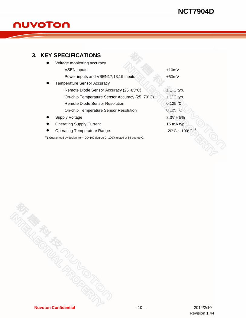
3. KEY SPECIFICATIONS Voltage monitoring accuracy
VSEN inputs ±10mV Power inputs and VSEN17,18,19 inputs ±60mV Temperature Sensor Accuracy
Remote Diode Sensor Accuracy (25~85°C) ± 1°C typ. On-chip Temperature Sensor Accuracy (25~70°C) ± 1°C typ. Remote Diode Sensor Resolution 0.125 ℃
On-chip Temperature Sensor Resolution 0.125 ℃
Supply Voltage 3.3V ± 5% Operating Supply Current 15 mA typ. Operating Temperature Range -20°C ~ 100°C *1 *1 Guaranteed by design from -20~100 degree C, 100% tested at 85 degree C.

NCT7904D
Nuvoton Confidential - 11 – 2014/2/10 Revision 1.44
4. PIN CONFIGURATION
NCT7904D
Nuvoton Confidential - 12 – 2014/2/10 Revision 1.44
5. PIN DESCRIPTION
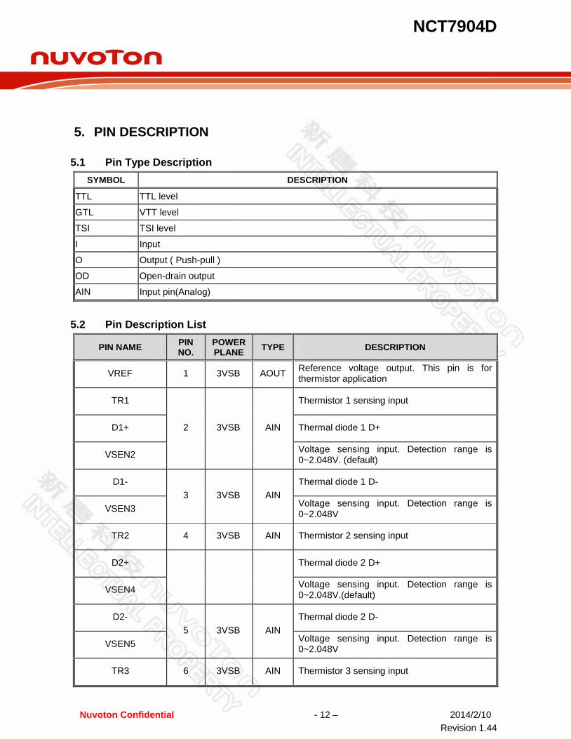
5.1 Pin Type Description SYMBOL DESCRIPTION
TTL TTL level
GTL VTT level
TSI TSI level
I Input
O Output ( Push-pull )
OD Open-drain output
AIN Input pin(Analog)
5.2 Pin Description List
PIN NAME PIN NO.
POWER PLANE TYPE DESCRIPTION
VREF 1 3VSB AOUT Reference voltage output. This pin is for thermistor application
TR1
2 3VSB AIN
Thermistor 1 sensing input
D1+ Thermal diode 1 D+
VSEN2 Voltage sensing input. Detection range is 0~2.048V. (default)
D1- 3 3VSB AIN
Thermal diode 1 D-
VSEN3 Voltage sensing input. Detection range is 0~2.048V
TR2 4 3VSB AIN Thermistor 2 sensing input
D2+
Thermal diode 2 D+
VSEN4 Voltage sensing input. Detection range is 0~2.048V.(default)
D2- 5 3VSB AIN
Thermal diode 2 D-
VSEN5 Voltage sensing input. Detection range is 0~2.048V
TR3 6 3VSB AIN Thermistor 3 sensing input
NCT7904D
Nuvoton Confidential - 13 – 2014/2/10 Revision 1.44
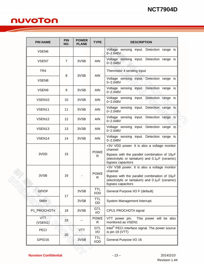
PIN NAME PIN NO.
POWER PLANE TYPE DESCRIPTION
VSEN6 Voltage sensing input. Detection range is 0~2.048V
VSEN7 7 3VSB AIN Voltage sensing input. Detection range is 0~2.048V
TR4 8 3VSB AIN
Thermistor 4 sensing input
VSEN8 Voltage sensing input. Detection range is 0~2.048V
VSEN9 9 3VSB AIN Voltage sensing input. Detection range is 0~2.048V
VSEN10 10 3VSB AIN Voltage sensing input. Detection range is 0~2.048V
VSEN11 11 3VSB AIN Voltage sensing input. Detection range is 0~2.048V
VSEN12 12 3VSB AIN Voltage sensing input. Detection range is 0~2.048V
VSEN13 13 3VSB AIN Voltage sensing input. Detection range is 0~2.048V
VSEN14 14 3VSB AIN Voltage sensing input. Detection range is 0~2.048V
3VDD 15 POWER
+3V VDD power. It is also a voltage monitor channel Bypass with the parallel combination of 10µF (electrolytic or tantalum) and 0.1µF (ceramic) bypass capacitors
3VSB 16 - POWER
+3V VSB power. It is also a voltage monitor channel Bypass with the parallel combination of 10µF (electrolytic or tantalum) and 0.1µF (ceramic) bypass capacitors
GPIOF 17
3VSB TTL I/OD General Purpose I/O F (default)
SMI# 3VSB TTL OD
System Management Interrupt.
P1_PROCHOT# 18 3VSB GTL I/O CPU1 PROCHOT# signal
VTT (VSEN1)
19 -- POWER
VTT power pin. This power will be also monitored as VSEN1
PECI 20
VTT GTL I/O
Intel® PECI interface signal. The power source is pin 19 (VTT)
GPIO16 3VSB TTL I/OD
General Purpose I/O 16

NCT7904D
Nuvoton Confidential - 14 – 2014/2/10 Revision 1.44
PIN NAME PIN NO.
POWER PLANE TYPE DESCRIPTION
SCL_TSI 3VSB TSI OD Clock line of AMD® SB_TSI interface
P1_THERMTRIP# 21
3VSB GTL I CPU1 THERMTRIP# signal. Pull-down it when unused.
SDA_TSI 3VSB TSI I/OD Data line of AMD® SB_TSI interface
CLKIN(33M, 14.318M, 48M) 22 3VSB TTL I
Clock input. 14.318MHz or 33MHz or 48MHz could be applied to this pin with corresponding register configuration. Default setting is for 33MHz This clock is for PECI and fan speed monitor
S_SMB_CLK 23 3VSB TTL I SMBus clock line for this device being slave device
S_SMB_DATA 24 3VSB TTL I/OD
SMBus data line for this device being slave device
M_SMB_CLK
25 3VSB
TTL OD
SMBus clock line for this device being master device
FANIN_11 TTL I Fan tachometer input
LED_EVNT_IN# TTL I An input event to trigger LED_OUT
M_SMB_DATA
26 3VSB
TTL I/OD
SMBus data line for this device being master device
FANIN_12 TTL I Fan tachometer input
LED_OUT TTL OD
When pin LED_EVNT_IN is asserted a low pulse, this pin will output a pulse to drive LED on or blinking
ADDR 27 3VSB TTL I SMBus slave address strap selection pin Strapped to low, the 7-bit address is 0101101 Strapped to high, the 7-bit address is 0101110
WDT_RSTOUT#
28 3VSB
TTL OD
Watch dog timer reset output
GPIOG TTL I/OD General Purpose I/O G (default)
VSEN17 AIN Voltage sensing input. Detection range is 0~3.3V
FANIN_1 29 3VSB TTL I Fan tachometer input
PWM1 30 3VSB TTL OD
Fan speed control PWM output. This is 5V tolerant
FANIN_2 31 3VSB TTL I Fan tachometer input

NCT7904D
Nuvoton Confidential - 15 – 2014/2/10 Revision 1.44
PIN NAME PIN NO.
POWER PLANE TYPE DESCRIPTION
PWM2 32 3VSB TTL OD
Fan speed control PWM output. This is 5V tolerant
FANIN_3 33 3VSB TTL I Fan tachometer input
PWM3 34 3VSB
TTL OD
Fan speed control PWM output. This is 5V tolerant
VSEN18 AIN Voltage sensing input. Detection range is 0~3.3V
FANIN_4 35 3VSB TTL I Fan tachometer input
PWM4/DCOUT 36 3VSB
TTL OD
AOUT
Fan speed control PWM or DC output. A register bit could be programmed to select PWM or DC mode. DC output is default mode. This is without 5V tolerant
VSEN19 AIN Voltage sensing input. Detection range is 0~3.3V
FANIN_5 37
3VSB TTL I Fan tachometer input.(default)
GPIO13 3VSB TTL I/OD
General Purpose I/O 13
FANIN_6 38
3VSB TTL I Fan tachometer input (default)
GPIO14 3VSB TTL I/OD
General Purpose I/O 14
FANIN_7 39
3VSB TTL I Fan tachometer input (default)
GPIO15 3VSB TTL I/OD
General Purpose I/O 15
FANIN_8 40
3VSB TTL I Fan tachometer input (default)
GPIOA 3VSB TTL I/OD
General Purpose I/O A
VOLT_ALM#
41
3VSB TTL OD
Voltage abnormal alert output signal ( active low )
FANIN_9 3VSB TTL I Fan tachometer input (default)
GPIOB 3VSB TTL I/OD
General Purpose I/O B
FAN_ALM# 42
3VSB TTL OD
Fan speed abnormal alert output signal ( active low )
FANIN_10 3VSB TTL I Fan tachometer input (default)
NCT7904D
Nuvoton Confidential - 16 – 2014/2/10 Revision 1.44
PIN NAME PIN NO.
POWER PLANE TYPE DESCRIPTION
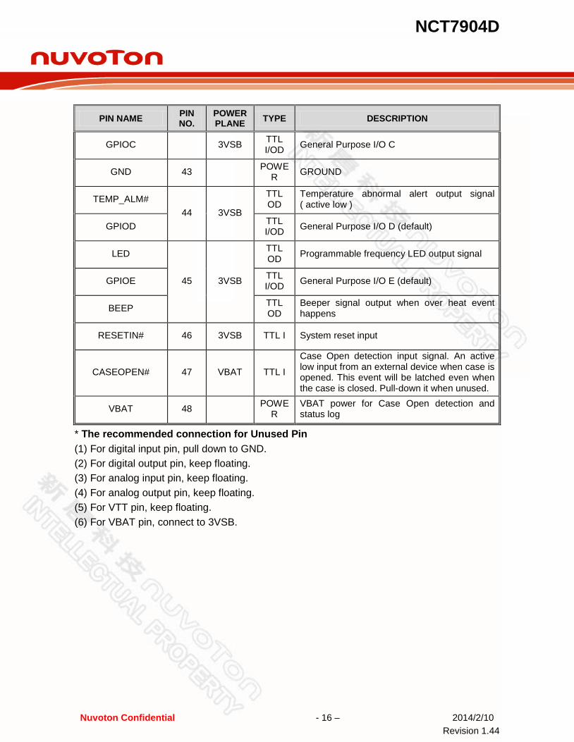
GPIOC 3VSB TTL I/OD
General Purpose I/O C
GND 43 POWER
GROUND
TEMP_ALM# 44 3VSB
TTL OD
Temperature abnormal alert output signal ( active low )
GPIOD TTL I/OD
General Purpose I/O D (default)
LED
45 3VSB
TTL OD Programmable frequency LED output signal
GPIOE TTL I/OD
General Purpose I/O E (default)
BEEP TTL OD
Beeper signal output when over heat event happens
RESETIN# 46 3VSB TTL I System reset input
CASEOPEN# 47 VBAT
TTL I
Case Open detection input signal. An active low input from an external device when case is opened. This event will be latched even when the case is closed. Pull-down it when unused.
VBAT 48 POWER
VBAT power for Case Open detection and status log
* The recommended connection for Unused Pin (1) For digital input pin, pull down to GND. (2) For digital output pin, keep floating. (3) For analog input pin, keep floating. (4) For analog output pin, keep floating. (5) For VTT pin, keep floating. (6) For VBAT pin, connect to 3VSB.

NCT7904D
Nuvoton Confidential - 17 – 2014/2/10 Revision 1.44
6. FUNCTIONAL DESCRIPTION
6.1 Access Interface NCT7904D provides SMBus interface, which is compliant with SMBus 2.0 specification. The 7-bit serial address is selected to be 0101101 or 0101110 by pin ADDR. When pin ADDR is strapped to low, the SMBus address is 0x5A(write)/0x5B(read) ; when pin ADDR is strapped to high, the SMBus address is 0x5C(write)/0x5D(read). NCT7904D supports the bus speed with 0~400KHz.
Data write to the internal register 6.1.1
Data read from the internal register 6.1.2
NCT7904D
Nuvoton Confidential - 18 – 2014/2/10 Revision 1.44
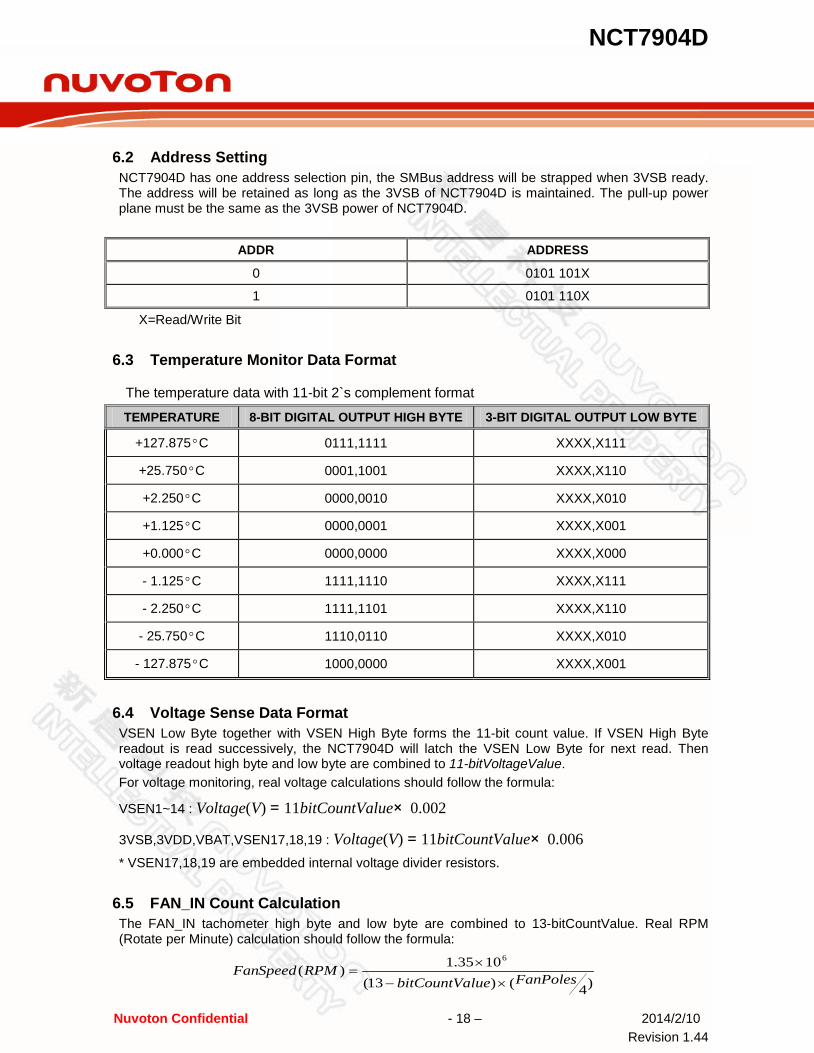
6.2 Address Setting NCT7904D has one address selection pin, the SMBus address will be strapped when 3VSB ready. The address will be retained as long as the 3VSB of NCT7904D is maintained. The pull-up power plane must be the same as the 3VSB power of NCT7904D.
ADDR ADDRESS
0 0101 101X
1 0101 110X
X=Read/Write Bit
6.3 Temperature Monitor Data Format
The temperature data with 11-bit 2`s complement format
TEMPERATURE 8-BIT DIGITAL OUTPUT HIGH BYTE 3-BIT DIGITAL OUTPUT LOW BYTE
+127.875°C 0111,1111 XXXX,X111
+25.750°C 0001,1001 XXXX,X110
+2.250°C 0000,0010 XXXX,X010
+1.125°C 0000,0001 XXXX,X001
+0.000°C 0000,0000 XXXX,X000
- 1.125°C 1111,1110 XXXX,X111
- 2.250°C 1111,1101 XXXX,X110
- 25.750°C 1110,0110 XXXX,X010
- 127.875°C 1000,0000 XXXX,X001
6.4 Voltage Sense Data Format VSEN Low Byte together with VSEN High Byte forms the 11-bit count value. If VSEN High Byte readout is read successively, the NCT7904D will latch the VSEN Low Byte for next read. Then voltage readout high byte and low byte are combined to 11-bitVoltageValue. For voltage monitoring, real voltage calculations should follow the formula:
VSEN1~14 : Voltage(V) = 11bitCountValue× 0.002
3VSB,3VDD,VBAT,VSEN17,18,19 : Voltage(V) = 11bitCountValue× 0.006 * VSEN17,18,19 are embedded internal voltage divider resistors.
6.5 FAN_IN Count Calculation The FAN_IN tachometer high byte and low byte are combined to 13-bitCountValue. Real RPM (Rotate per Minute) calculation should follow the formula:
)4()13(1035.1)(
6
FanPolesluebitCountVaRPMSpeedFan
×−
×=

NCT7904D
Nuvoton Confidential - 19 – 2014/2/10 Revision 1.44
In this formula, FanPole stands for the number of NS pole pairs inside the fan. Normally an N-S-N-S Fan (FanPole=4) generates 2 pulses after completing one rotation.
6.6 FAN_OUT Duty Cycle/DC output Calculation The NCT7904D provides 4 set of PWM and 1 set of DC output for fan speed control. The duty cycle of PWM can be programmed by an 8-bit register. The expression of duty cycle can be represented as follow formula:
%100255
ValueRegister bit -8 Programmed(%)cycleDuty ×=−
The DC output can be programmed by an 8-bit register. The expression of DC level can be represented as follow formula:
255ValueRegister bit -8 Programmed3)(Voutput DC ×= VDD
6.7 Fan Speed Control Except for traditional Fan Duty control, the latest closed loop fan control (RPM Mode) has been provided by the NCT7904D. Due to PECI negative temperature format, the fan control also supports negative temperature representation. It would be much easy to implement fan control by PECI reading. In addition to PECI CPU temperature, the NCT7904D also supports fan control, which is responded to CPU power. In Smart Fan Mode, there are some Fan control parameters as below descriptions:
Step Up Time / Step Down Time 6.7.1Smart Fan is designed for the smooth operation of the fan. The Up Time / Down Time register defines the time interval between successive duty increases or decreases. If this value is set too small, the fan will not have enough time to speed up after tuning the duty and sometimes may result in unstable fan speed. On the other hand, if Up Time / Down Time is set too large, the fan may not work fast enough to dissipate the heat. This register should never be set to 0, otherwise, the fan duty will be abnormal.
Fan Output Nonstop Value 6.7.2It takes some time to bring a fan from still to working state. Therefore, Nonstop value are designed with a minimum fan output to keep the fan working when the system does not require the fan to help reduce heat but still want to keep the fast response time to speed up the fan.
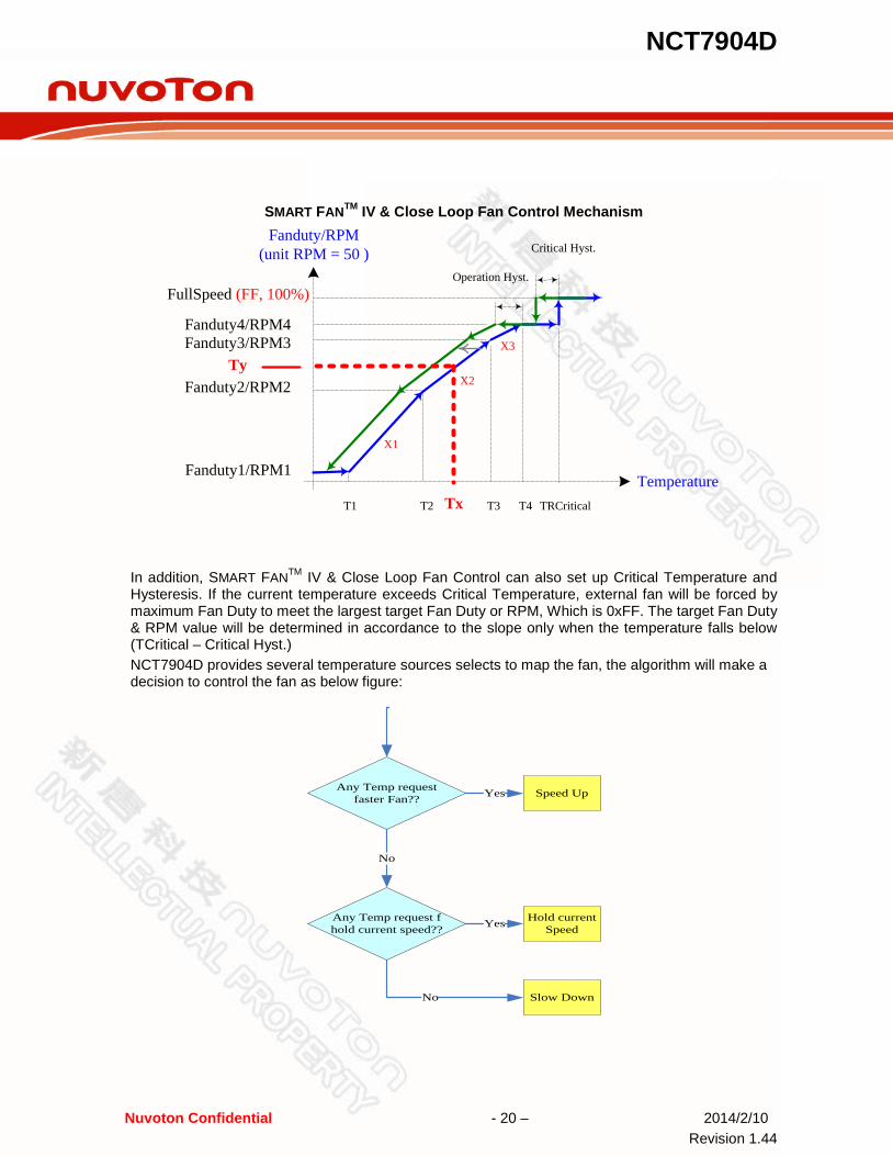
Smart Fan Control Table 6.7.3SMART FANTM IV and Close Loop Fan Control Mode offer 4 slopes to control the fan speed. The 3 slopes can be obtained by setting FanDuty/RPM1~FanDuty/RPM4 and T1~T4 through the registers. When the temperature rises, FAN Output will calculate the target Fan Duty/RPM based on the current slope. For example, assuming Tx is the current temperature and Fan Duty/RPMy is the target, then the slope:
( ) ( )( )23
2/23/32TT
RPMFanDutyRPMFanDutyX−−
=
Fan Output:
( ) ( ) 2222arg XTTxRPMorFanDutyRPMorFanDutyetT ⋅−+=
NCT7904D
Nuvoton Confidential - 20 – 2014/2/10 Revision 1.44
SMART FANTM IV & Close Loop Fan Control Mechanism
Fanduty1/RPM1
Fanduty2/RPM2
FullSpeed (FF, 100%)Operation Hyst.
TRCritical
Critical Hyst.
T1 T2 T3 T4
X2
X1
Fanduty3/RPM3Fanduty4/RPM4
X3
Tx
Ty
Fanduty/RPM(unit RPM = 50 )
Temperature
In addition, SMART FANTM IV & Close Loop Fan Control can also set up Critical Temperature and Hysteresis. If the current temperature exceeds Critical Temperature, external fan will be forced by maximum Fan Duty to meet the largest target Fan Duty or RPM, Which is 0xFF. The target Fan Duty & RPM value will be determined in accordance to the slope only when the temperature falls below (TCritical – Critical Hyst.) NCT7904D provides several temperature sources selects to map the fan, the algorithm will make a decision to control the fan as below figure:
Any Temp request faster Fan??
Any Temp request f hold current speed??
No
No
Speed Up
Hold current Speed
Slow Down
Yes
Yes
NCT7904D
Nuvoton Confidential - 21 – 2014/2/10 Revision 1.44
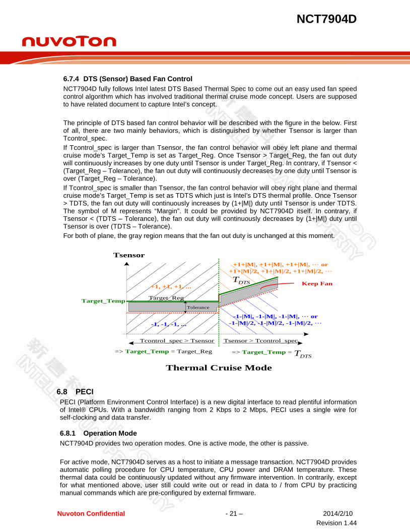
DTS (Sensor) Based Fan Control 6.7.4NCT7904D fully follows Intel latest DTS Based Thermal Spec to come out an easy used fan speed control algorithm which has involved traditional thermal cruise mode concept. Users are supposed to have related document to capture Intel’s concept. The principle of DTS based fan control behavior will be described with the figure in the below. First of all, there are two mainly behaviors, which is distinguished by whether Tsensor is larger than Tcontrol_spec. If Tcontrol_spec is larger than Tsensor, the fan control behavior will obey left plane and thermal cruise mode’s Target_Temp is set as Target_Reg. Once Tsensor > Target_Reg, the fan out duty will continuously increases by one duty until Tsensor is under Target_Reg. In contrary, if Tsensor < (Target_Reg – Tolerance), the fan out duty will continuously decreases by one duty until Tsensor is over (Target_Reg – Tolerance). If Tcontrol_spec is smaller than Tsensor, the fan control behavior will obey right plane and thermal cruise mode’s Target_Temp is set as TDTS which just is Intel’s DTS thermal profile. Once Tsensor > TDTS, the fan out duty will continuously increases by (1+|M|) duty until Tsensor is under TDTS. The symbol of M represents “Margin”. It could be provided by NCT7904D itself. In contrary, if Tsensor < (TDTS – Tolerance), the fan out duty will continuously decreases by (1+|M|) duty until Tsensor is over (TDTS – Tolerance). For both of plane, the gray region means that the fan out duty is unchanged at this moment.
Target_TempTolerance
Tsensor
Thermal Cruise Mode
DTST
-1, -1, -1, ...
+1, +1, +1, ...
Tsensor > Tcontrol_spec
=> Target_Temp = DTST
Tcontrol_spec > Tsensor
Target_Reg
=> Target_Temp = Target_Reg
+1+|M|, +1+|M|, +1+|M|, … or +1+|M|/2, +1+|M|/2, +1+|M|/2, …
-1-|M|, -1-|M|, -1-|M|, … or -1-|M|/2, -1-|M|/2, -1-|M|/2, …
Keep Fan
6.8 PECI PECI (Platform Environment Control Interface) is a new digital interface to read plentiful information of Intel® CPUs. With a bandwidth ranging from 2 Kbps to 2 Mbps, PECI uses a single wire for self-clocking and data transfer.
Operation Mode 6.8.1NCT7904D provides two operation modes. One is active mode, the other is passive. For active mode, NCT7904D serves as a host to initiate a message transaction. NCT7904D provides automatic polling procedure for CPU temperature, CPU power and DRAM temperature. These thermal data could be continuously updated without any firmware intervention. In contrarily, except for what mentioned above, user still could write out or read in data to / from CPU by practicing manual commands which are pre-configured by external firmware.

NCT7904D
Nuvoton Confidential - 22 – 2014/2/10 Revision 1.44
In passive mode, NCT7904D just monitor the message over the PECI bus with silence and then only extract CPU’s DTS thermal data for its fan speed control purpose.
CPU Temperature and Power Reporting 6.8.2In NCT7904D, it supports CPU temperature and power reporting. And both of reading could be associated to NCT7904D’s fan control algorithm. For CPU temperature, by interfacing to the Digital Thermal Sensor (DTS) in the Intel® CPU, PECI reports a negative temperature (in counts) relative to the processor’s temperature at which the thermal control circuit (TCC) is activated. At the TCC Activation temperature, the Intel CPU will operate at reduced performance to prevent the device from thermal damage. The PECI temperature values returning from the CPU are in “counts” which are approximately linear in relation to changes in temperature in degrees centigrade. However, this linearity is approximate and cannot be guaranteed over the entire range of PECI temperatures. For further information, refer to the PECI specification. However NCT7904D has a biasing factor for customer to characterize the relation between “counts” and “temperature”. Figure A shows a typical fan speed (PWM duty cycle) and PECI temperature relationship. SMART FANTM IV
Tcontrol TCC Activation
Duty1
Duty2
-20 0-10
PECI Temperature (counts)
Fan Speed(PWM Duty Cycle)
Fig. A PECI Temperature
In this illustration, when PECI temperature is -20, the PWM duty cycle for fan control is at Duty2. When CPU is getting hotter and the PECI temperature is -10, the PWM duty cycle is at Duty1. At Tcontrol PECI temperature, the recommendation from Intel is to operate the CPU fan at full speed. Therefore Duty1 is 100% if this recommendation is followed. The value of Tcontrol can be obtained by reading the related Machine Specific Register (MSR) in the Intel CPU. The Tcontrol MSR address is usually in the BIOS Writer’s guide for the CPU family in question. Refer to the relevant CPU documentation from Intel for more information. In this example, Tcontrol is -10. When the PECI temperature is below -20, the duty cycle is fixed at Duty2 to maintain a minimum (and constant) RPM for the CPU fan. For CPU power reporting, the NCT7904D routinely retrieves CPU energy and then convert it to power. The refreshing rate of power is 0.3 sec. In order to minimize the effect of suddenly huge power changing, the running time average algorithm has been implemented.

NCT7904D
Nuvoton Confidential - 23 – 2014/2/10 Revision 1.44
DRAM Thermal Data Reporting 6.8.3NCT7904D can automatically report all 24 DIMMs thermal status which are provided by Intel CPU0 and CPU1 agent. In addition to each DIMM temperature, NCT7904D also records the highest DIMM temperature in the specific channel. Here is the relationship among CPU, Channel and DIMM. Both the Channel Index<2:0> and DIMM Index<5:3> follow PECI3.0 RdPkgConfig() command format.
Agent Address Channel_Index<2:0> DIMM Index<5:3> Register Location
CPU0_30h
Channel_0
DIMM_0 T_D0C0_C0
DIMM_1 T_D1C0_C0
DIMM_2 T_D2C0_C0
Channel_1 DIMM_0 T_D0C1_C0
DIMM_1 T_D1C1_C0
DIMM_2 T_D2C1_C0
Channel_2 DIMM_0 T_D0C2_C0
DIMM_1 T_D1C2_C0
DIMM_2 T_D2C2_C0
Channel_3 DIMM_0 T_D0C2_C0
DIMM_1 T_D1C2_C0
DIMM_2 T_D2C2_C0
CPU1_31h
Channel_0 DIMM_0 T_D0C0_C1
DIMM_1 T_D1C0_C1
DIMM_2 T_D2C0_C1
Channel_1 DIMM_0 T_D0C1_C1
DIMM_1 T_D1C1_C1
DIMM_2 T_D2C1_C1
Channel_2 DIMM_0 T_D0C2_C1
DIMM_1 T_D1C2_C1
DIMM_2 T_D2C2_C1
Channel_3 DIMM_0 T_D0C3_C1
DIMM_1 T_D1C3_C1
DIMM_2 T_D2C3_C1
PECI Listening 6.8.4It provides another way to obtain CPU’s DTS thermal data. NCT7904D only recognizes GetTemp() command. Once GetTemp() appears on PECI bus and entire message is without FCS error, the CPU’s DTS temperature will be extracted and recorded. These data could be temperature source of fan speed control.

NCT7904D
Nuvoton Confidential - 24 – 2014/2/10 Revision 1.44
6.9 SMI# Output
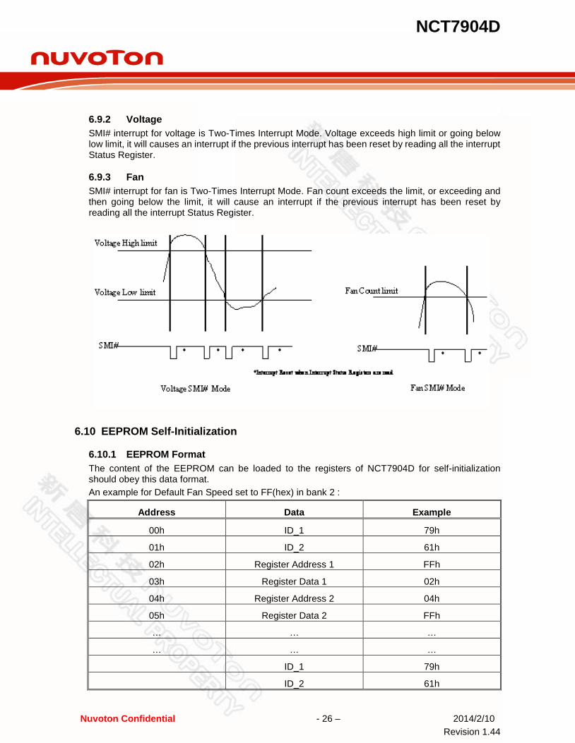
Temperature 6.9.1SMI# for temperature monitoring provides 3 modes.
6.9.1.1. Comparator Interrupt Mode Temperature exceeding Twarning causes an interrupt and this interrupt will be reset when reading all of the Interrupt Status Registers. Once an interrupt event has occurred by exceeding Twarning, then reset, if the temperature remains above the Twarning Hysteresis, the interrupt will occur again when the next conversion has completed. If an interrupt event has occurred by exceeding Twarning and not reset, the interrupts will not occur again. The interrupts will continue to occur in this manner until the temperature goes below Twarning Hysteresis.
6.9.1.2. Two-Times Interrupt Mode Temperature exceeding Tcritical / Twarning causes an interrupt and then temperature going below Tcritical Hysteresis / Twarning Hysteresis will also cause an interrupt if the previous interrupt has been reset by reading all the Interrupt Status Register. Once an interrupt event has occurred by exceeding Tcritical / Twarning, then reset, if the temperature remains above the Tcritical Hysteresis / Twarning Hysteresis, the interrupt will not occur.
6.9.1.3. One-Time Interrupt Mode Temperature exceeding Tcritical / Twarning causes an interrupt and then temperature going below Tcritical Hysteresis / Twarning Hysteresis will not cause an interrupt. Once an interrupt event has occurred by exceeding Tcritical / Twarning, then going below Tcritical Hysteresis / Twarning Hysteresis, an interrupt will not occur again until the temperature exceeding Tcritical / Twarning.
SMI comparator mode

NCT7904D
Nuvoton Confidential - 25 – 2014/2/10 Revision 1.44
SMI two time mode
SMI one time mode
NCT7904D
Nuvoton Confidential - 26 – 2014/2/10 Revision 1.44
Voltage 6.9.2SMI# interrupt for voltage is Two-Times Interrupt Mode. Voltage exceeds high limit or going below low limit, it will causes an interrupt if the previous interrupt has been reset by reading all the interrupt Status Register.
Fan 6.9.3SMI# interrupt for fan is Two-Times Interrupt Mode. Fan count exceeds the limit, or exceeding and then going below the limit, it will cause an interrupt if the previous interrupt has been reset by reading all the interrupt Status Register.
6.10 EEPROM Self-Initialization
EEPROM Format 6.10.1The content of the EEPROM can be loaded to the registers of NCT7904D for self-initialization should obey this data format. An example for Default Fan Speed set to FF(hex) in bank 2 :
Address Data Example
00h ID_1 79h
01h ID_2 61h
02h Register Address 1 FFh
03h Register Data 1 02h
04h Register Address 2 04h
05h Register Data 2 FFh
… … …
… … …
ID_1 79h
ID_2 61h
NCT7904D
Nuvoton Confidential - 27 – 2014/2/10 Revision 1.44
Chip Initialization 6.10.2When NCT7904D detects power-on-reset, initialization process will start loading data from EEPROM. NCT7904D SMBUS (M_SMB_CLK, M_SMB_DATA) will be a master and issue consecutive read byte commands (EEPROM address is A0h). NCT7904D will check receive data to decide that which actions should be followed.
Case 1 : No acknowledge in first transaction, NCT7904D will terminate the initialization process to normal. And set LD_FAIL and LD_FINISH to 1 to note host the load status. Case 2 : NCT7904D will check first two bytes by ID_1 and ID_2. If match, the process will continue. Otherwise, the process will terminate like Case 1. Case 3 : Two bytes as a unit. NCT7904D will see first as the address of the register and second as the data. Sequentially, NCT7904D will write the data to the specific address. Case 4 : When receiving the unit which store the data (ID_2 following ID_1), NCT7904D will stop initialization and back to normal and set LD_FAIL to 0 and LD_FINISH to 1 to note host the load status. Otherwise, the access will keep going.
The EEPROM loading would be started from NCT7904D power-on immediately, when implements the EEPROM self-initialization, the requested 3VSB power rising time must less than 60uS.
Note:
1. LD_FAIL and LD_FINISH are in address 00h in bank 0.
6.11 PCH Thermal Data Report
PCH Thermal Read 6.11.1When enable PCH read function (set EN_PCH_RD to 1), NCT7904D SMBUS (M_SMB_CLK, M_SMB_DATA) will be a master and issue consecutive block read commands (PCH address can be configuration). NCT7904D will store the received data to the registers (F0h~FDh in bank 0) by PCH data format.
PCH Thermal Data Format 6.11.2The PCH Thermal data may appear in either Byte 0 or Byte 1 depending on the specific ME firmware in use. Please contact Intel directly for information on your specific ME Firmware implementation.
6.12 SMBus Master Auto Read External Thermal Sensor
External Thermal Sensor Setting 6.12.1Before using this function, there are several registers must be set:
1. Configuration external sensor SMBus address and command where temperature store in. (6Ch ~ 73h in bank 2). 2. Set relative port enable and enable external temperature read (6Ah in bank 2).
Temperature Read Process 6.12.2After proper setting, NCT7904D will auto read, by setting, external sensor temperature from SMBus master I/F. The read temperature will be stored in the registers (BCh ~ BFh in bank 0), respectively. These temperatures can be the sources of the fan controller in NCT7904D. Any not enable port can normally be the virtual temperature simply written by host to do advanced fan control.

NCT7904D
Nuvoton Confidential - 28 – 2014/2/10 Revision 1.44
6.13 PROCHOT# Behavior
PROCHOT# Input 6.13.1When enable PROCHOT# input monitor function (set EN_PH1 to 1 in bank 0, PH1_MD to 1 in bank 1), NCT7904D will monitor P1_PROCHOT# pin, count the time between two falling edge as P1_PROCHOT#_DVAL[7:0] and the time between one rising edge to one falling edge P1_PROCHOT#_NVAL[7:0], and stores these two to the registers. System management can monitor these two values to know the thermal status for relative CPU. The timer to the counter is settable from register, and the default is 22us.
PROCHOT# Output 6.13.2When enable PROCHOT# output function (set EN_PH1 to 1 in bank 0, PH1_MD to 0 in bank 1), NCT7904D will drive low to P1_PROCHOT# pin based on several thermal events over heat. There are three temperature sources listed as blow, Source 1 : 4 remote temperature inputs or build-in thermal diode temperature Source 2 : Up to 8 CPU temperatures Source 3 : Up to 4 CPU Powers (by PECI) The frequency and duty cycle of PROCHOT# output are settable by PH1_FSEL[1:0] and PH1_DC[3:0], respectively.
6.14 LED Behavior
Event Trigger LED 6.14.1When enable LED function (set EN_E_LED to 1), NCT7904D will detect LED_EVNT_IN# pin as the drive condition for LED_OUT. LED pin will be float when LED_EVNT_IN# pin is detected high, and LED pin will drive low when LED_EVNT_IN# is detected low. LED driving low frequency and polarity can be settable.
Programmable LED 6.14.2When enable programmable LED function (set EN_P_LED to 1), NCT7904D will drive register data P_LED_DATA to LED pin. Drive low frequency and polarity can be settable.
6.15 BEEP Function
Output Signaling 6.15.1Output signaling for BEEP is controlled by an internal signal mixer. The baseband signal is a period signal which is at frequency 1Hz with duty cycle 50% (i.e. the period for high and low level is 500ms.) The high level of the baseband signal will mix the signal which is at frequency 700Hz with duty cycle 50%, and the low level of the baseband signal will mix the signal which is at frequency 350Hz with duty cycle 50%, causing the ambulance sound for alarm to users.
BEEP Activation 6.15.2When enable BEEP function (set EN_BEEP to 1), NCT7904D will drive the signal to BEEP pin when BEEP sources selected and over limitation. Otherwise, NCT7904D will float the pin. The sources are defined in relative registers.

NCT7904D
Nuvoton Confidential - 29 – 2014/2/10 Revision 1.44
6.16 THERMTRIP# Function
Power by VSB 6.16.1When enable THERMTRIP function (set EN_THRM to 1), NCT7904D will detect low and log the signal to THRM_STS register. The THRM_STS register will be cleared by setting the CLR_THRM register to 1 and the CLR_THRM will be auto cleared.
Power Only by VBAT 6.16.2NCT7904D will keep the THRM_STS register when VBAT power-on, losing the data when VBAT power-off.
NCT7904D
Nuvoton Confidential - 30 – 2014/2/10 Revision 1.44
7. REGISTER DESCRIPTION
7.1 Bank 0 REGISTER DETAIL
Global Control Register 7.1.1Location: Bank 0 Address 00HEX Type: Read/Write Reset: Power On Reset Default Value: 01HEX
BIT DESCRIPTION
7 INIT_RST Registers initial reset (Auto be cleared when reset process completed)
6 Reserved
5 LD_FAIL 0 = EEPROM present and no error happened 1 = EEPROM not present or error happened
4 LD_FINISH 0 = EEPROM data load processing 1 = EEPROM data load finished
3
LOCK 0 = RESETIN# will reset registers 1 = RESETIN# will not reset registers (This bit will be also cleared when set INIT_RST)
2 Reserved
1-0
CLKIN_SEL[1:0] 00BIN = 14.318MHz 01BIN = 33MHz (default) 10BIN = 48MHz 11BIN = Reserved
SMB Slave Address Register 7.1.2Location: Bank 0 Address 0CHEX Type: Read Only Reset: Power On Reset Default Value: 5AHEX/5CHEX
BIT DESCRIPTION
7-0 SMB_SLV_ADDR[7:0] 5AHEX = ADDR pin strapped low 5CHEX = ADDR pin strapped high

NCT7904D
Nuvoton Confidential - 31 – 2014/2/10 Revision 1.44
Nuvoton Vendor ID Register 7.1.3Location: Bank 0 Address 0DHEX Type: Read Only Reset: Power On Reset Default Value: 50HEX
BIT DESCRIPTION
7-0 VENDOR_ID[7:0]
Nuvoton Chip ID Register 7.1.4Location: Bank 0 Address 0EHEX Type: Read Only Reset: Power On Reset Default Value: C5HEX
BIT DESCRIPTION
7-0 CHIP_ID[7:0]
Nuvoton Device ID Register 7.1.5Location: Bank 0 Address 0FHEX Type: Read Only Reset: Power On Reset Default Value: 5xHEX
BIT DESCRIPTION
7-0 DEVICE_ID[7:0]
Programmable LED Register 7.1.6Location: Bank 0 Address 18HEX Type: Read / Write Reset: Power On Reset RESETIN# with LOCK=0 Default Value: 00HEX
BIT DESCRIPTION
7 EN_P_LED 0 = Disable 1 = Enable
6 P_LED_POL 0 = LED output active low 1 = LED output active high
5 P_LED_DATA 0 = Output don’t drive 1 = Output drive
4-3 Reserved
2-0 P_LED_FSEL[2:0]

NCT7904D
Nuvoton Confidential - 32 – 2014/2/10 Revision 1.44
BIT DESCRIPTION 000BIN = 4Hz 001BIN = 2Hz 010BIN = 1Hz 011BIN = 0.5Hz 100BIN = 0.25Hz 101BIN = 0.125Hz 110BIN = 0.0625Hz 111BIN = 0Hz
Event Control LED Register 7.1.7Location: Bank 0 Address 19HEX Type: Read / Write Reset: Power On Reset RESETIN# with LOCK=0 Default Value: 00HEX
BIT DESCRIPTION
7 EN_E_LED 0 = Disable 1 = Enable (LED_OUT will controlled by LED_EVNT_IN#)
6 E_LED_POL 0 = LED output active low 1 = LED output active high
5-3 Reserved 2-0 E_LED_FSEL[2:0]
000BIN = 4Hz 001BIN = 2Hz 010BIN = 1Hz 011BIN = 0.5Hz 100BIN = 0.25Hz 101BIN = 0.125Hz 110BIN = 0.0625Hz 111BIN = 0Hz
Monitor Enable Control Register 7.1.8Location:
VT_ADC_CTRL0 - Bank 0 Address 20HEX VT_ADC_CTRL1 - Bank 0 Address 21HEX
VT_ADC_CTRL2 - Bank 0 Address 22HEX
PH_CTRL0 - Bank 0 Address 23HEX
FANIN_CTRL0 - Bank 0 Address 24HEX
FANIN_CTRL1 - Bank 0 Address 25HEX
DTS_T_CTRL0 - Bank 0 Address 26HEX
DTS_T_CTRL1 - Bank 0 Address 27HEX
DTS_P_CTRL0 - Bank 0 Address 28HEX

NCT7904D
Nuvoton Confidential - 33 – 2014/2/10 Revision 1.44
Type: Read / Write Reset: Power On Reset RESETIN# with LOCK=0 VT_ADC_CTRL0 – Voltage Temperature Monitoring Control Register Location: Bank 0 Address 20HEX
Default Value: FFHEX
BIT DESCRIPTION
7 EN_VSEN8 – Enable VSEN8 voltage monitoring. 0 = Disable 1 = Enable
6 EN_VSEN7 – Enable VSEN7 voltage monitoring. 0 = Disable 1 = Enable
5 EN_VSEN6 – Enable VSEN6 voltage monitoring. 0 = Disable 1 = Enable
4 EN_VSEN5 – Enable VSEN5 voltage monitoring. 0 = Disable 1 = Enable
3 EN_VSEN4 – Enable VSEN4 voltage monitoring. 0 = Disable 1 = Enable
2 EN_VSEN3 – Enable VSEN3 voltage monitoring. 0 = Disable 1 = Enable
1 EN_VSEN2 – Enable VSEN2 voltage monitoring. 0 = Disable 1 = Enable
0 EN_VSEN1 – Enable VSEN1 voltage monitoring. 0 = Disable 1 = Enable
VT_ADC_CTRL1 – Voltage Temperature Monitoring Control Register Location: Bank 0 Address 21HEX
Default Value: 7FHEX
BIT DESCRIPTION
7 EN_VBAT – Enable VBAT voltage monitoring. 0 = Disable 1 = Enable
6 EN_3VDD – Enable 3VDD voltage monitoring. 0 = Disable 1 = Enable
5 EN_VSEN14 – Enable VSEN14 voltage monitoring. 0 = Disable
NCT7904D
Nuvoton Confidential - 34 – 2014/2/10 Revision 1.44
BIT DESCRIPTION 1 = Enable
4 EN_VSEN13 – Enable VSEN13 voltage monitoring. 0 = Disable 1 = Enable
3 EN_VSEN12 – Enable VSEN12 voltage monitoring. 0 = Disable 1 = Enable
2 EN_VSEN11 – Enable VSEN11 voltage monitoring. 0 = Disable 1 = Enable
1 EN_VSEN10 – Enable VSEN10 voltage monitoring. 0 = Disable 1 = Enable
0 EN_VSEN9 – Enable VSEN9 voltage monitoring. 0 = Disable 1 = Enable
VT_ADC_CTRL2 – Voltage Temperature Monitoring Control Register Location: Bank 0 Address 22HEX
Default Value: 03HEX
BIT DESCRIPTION
7-5 Reserved
4 EN_VSEN19 – Enable VSEN19 voltage monitoring. 0 = Disable (This pin will change to PWM4/DCOUT) 1 = Enable
3 EN_VSEN18 – Enable VSEN18 voltage monitoring. 0 = Disable (This pin will change to PWM3) 1 = Enable
2 EN_VSEN17 – Enable VSEN17 voltage monitoring. 0 = Disable (This pin will change to WDT_RSTOUT#/GPIOG) 1 = Enable
1 EN_LTD – Enable local temperature monitoring. 0 = Disable 1 = Enable
0 EN_V3VSB – Enable V3VSB voltage monitoring. 0 = Disable 1 = Enable
PH_CTRL0 – PROCHOT Monitoring Control Register Location: Bank 0 Address 23HEX
Default Value: 01HEX
BIT DESCRIPTION

NCT7904D
Nuvoton Confidential - 35 – 2014/2/10 Revision 1.44
BIT DESCRIPTION
7-1 Reserved 0 EN_PH1 – Enable P1_PROCHOT# monitoring.
0 = Disable 1 = Enable
FANIN_CTRL0 – FANIN Monitoring Control Register Location: Bank 0 Address 24HEX
Default Value: FFHEX
BIT DESCRIPTION
7 EN_FANIN_8 – Enable FANIN_8 monitoring. 0 = Disable 1 = Enable
6 EN_FANIN_7 – Enable FANIN_7 monitoring. 0 = Disable 1 = Enable
5 EN_FANIN_6 – Enable FANIN_6 monitoring. 0 = Disable 1 = Enable
4 EN_FANIN_5 – Enable FANIN_5 monitoring. 0 = Disable 1 = Enable
3 EN_FANIN_4 – Enable FANIN_4 monitoring. 0 = Disable 1 = Enable
2 EN_FANIN_3 – Enable FANIN_3 monitoring. 0 = Disable 1 = Enable
1 EN_FANIN_2 – Enable FANIN_2 monitoring. 0 = Disable 1 = Enable
0 EN_FANIN_1 – Enable FANIN_1 monitoring. 0 = Disable 1 = Enable
FANIN_CTRL1 – FANIN Monitoring Control Register Location: Bank 0 Address 25HEX
Default Value: 03HEX
BIT DESCRIPTION
7-4 Reserved 3 EN_FANIN_12 – Enable FANIN_12 monitoring.
0 = Disable 1 = Enable
2 EN_FANIN_11 – Enable FANIN_11 monitoring.

NCT7904D
Nuvoton Confidential - 36 – 2014/2/10 Revision 1.44
BIT DESCRIPTION 0 = Disable 1 = Enable
1 EN_FANIN_10 – Enable FANIN_10 monitoring. 0 = Disable 1 = Enable
0 EN_FANIN_9 – Enable FANIN_9 monitoring. 0 = Disable 1 = Enable
DTS_T_CTRL0 – Digital Temperature Monitoring Control Register Location: Bank 0 Address 26HEX
Default Value: 0FHEX
BIT DESCRIPTION
7-4 Reserved 3 EN_TCPU4 – Enable DTS CPU4 temperature monitoring (PECI/TSI).
0 = Disable 1 = Enable
2 EN_TCPU3 – Enable DTS CPU3 temperature monitoring (PECI/TSI). 0 = Disable 1 = Enable
1 EN_TCPU2 – Enable DTS CPU2 temperature monitoring (PECI/TSI). 0 = Disable 1 = Enable
0 EN_TCPU1 – Enable DTS CPU1 temperature monitoring (PECI/TSI). 0 = Disable 1 = Enable
DTS_T_CTRL1 – Digital Temperature Monitoring Control Register Location: Bank 0 Address 27HEX
Default Value: 0FHEX
BIT DESCRIPTION
7-4 Reserved 3 EN_TCPU8 – Enable DTS CPU8 temperature monitoring (TSI).
0 = Disable 1 = Enable
2 EN_TCPU7 – Enable DTS CPU7 temperature monitoring (TSI). 0 = Disable 1 = Enable
1 EN_TCPU6 – Enable DTS CPU6 temperature monitoring (TSI). 0 = Disable 1 = Enable
0 EN_TCPU5 – Enable DTS CPU5 temperature monitoring (TSI). 0 = Disable 1 = Enable

NCT7904D
Nuvoton Confidential - 37 – 2014/2/10 Revision 1.44
DTS_P_CTRL0 – Digital Power Monitoring Control Register Location: Bank 0 Address 28HEX
Default Value: 0FHEX
BIT DESCRIPTION
7-4 Reserved 3 EN_PCPU4 – Enable DTS CPU4 power monitoring (PECI).
0 = Disable 1 = Enable
2 EN_PCPU3 – Enable DTS CPU3 power monitoring (PECI). 0 = Disable 1 = Enable
1 EN_PCPU2 – Enable DTS CPU2 power monitoring (PECI). 0 = Disable 1 = Enable
0 EN_PCPU1 – Enable DTS CPU1 power monitoring (PECI). 0 = Disable 1 = Enable
Monitor Configuration Register 7.1.9Location: VT_ADC_VOL_PO - Bank 0 Address 2CHEX VT_ADC_LTD_PO - Bank 0 Address 2DHEX
VT_ADC_MD - Bank 0 Address 2EHEX VT_ADC_PO0 - Bank 0 Address 2FHEX
VT_ADC_PO1 - Bank 0 Address 30HEX
VT_ADC_PO2 - Bank 0 Address 31HEX
VT_ADC_PO3 - Bank 0 Address 32HEX
Type: Read / Write Reset: Power On Reset RESETIN# with LOCK=0 VT_ADC_VOL_PO – Voltage Post Offset Register Location: Bank 0 Address 2CHEX
Default Value: 00HEX
BIT DESCRIPTION
7-0 VT_ADC_VOL_PO[7:0] Post offset adjustment in voltage
VT_ADC_LTD_PO – LTD Temperature Post Offset Register Location: Bank 0 Address 2DHEX
Default Value: 00HEX
BIT DESCRIPTION

NCT7904D
Nuvoton Confidential - 38 – 2014/2/10 Revision 1.44
BIT DESCRIPTION
7-0 VT_ADC_LTD_PO[7:0] Post offset adjustment in LTD temperature
VT_ADC_MD – Voltage Temperature Mode Control Register Location: Bank 0 Address 2EHEX
Default Value: 00HEX
BIT DESCRIPTION 7-6 VSEN89_MD[1:0]
00BIN = Voltage monitoring 01BIN = Reserved 10BIN = Reserved 11BIN = Temperature monitoring (thermistor) When set to thermistor mode, the Pin.8 will be TR4 function, the Pin.9 will be VSEN9 function.
5-4 VSEN67_MD[1:0] 00BIN = Voltage monitoring 01BIN = Reserved 10BIN = Reserved 11BIN = Temperature monitoring (thermistor) When set to thermistor mode, the Pin.6 will be TR3 function, the Pin.7 will be VSEN7 function.
3-2 VSEN45_MD[1:0] 00BIN = Voltage monitoring 01BIN = Temperature monitoring (thermal diode current mode) 10BIN = Reserved 11BIN = Temperature monitoring (thermistor) When set to thermistor mode, the Pin.4 will be TR2 function, the Pin.5 will be VSEN5 function.
1-0 VSEN23_MD[1:0] 00BIN = Voltage monitoring 01BIN = Temperature monitoring (thermal diode current mode) 10BIN = Reserved 11BIN = Temperature monitoring (thermistor) When set to thermistor mode, the Pin.2 will be TR1 function, the Pin.3 will be VSEN3 function.
VT_ADC_PO0 – Voltage Temperature Post Offset Register Location: Bank 0 Address 2FHEX
Default Value: 00HEX
BIT DESCRIPTION 7-0 VSEN23_PO[7:0]
Post offset adjustment when VSEN23_MD[1:0] in temperature mode
VT_ADC_PO1 – Voltage Temperature Post Offset Register

NCT7904D
Nuvoton Confidential - 39 – 2014/2/10 Revision 1.44
Location: Bank 0 Address 30HEX
Default Value: 00HEX
BIT DESCRIPTION 7-0 VSEN45_PO[7:0]
Post offset adjustment when VSEN45_MD[1:0] in temperature mode
VT_ADC_PO2 – Voltage Temperature Post Offset Register Location: Bank 0 Address 31HEX
Default Value: 00HEX
BIT DESCRIPTION
7-0 VSEN67_PO[7:0] Post offset adjustment when VSEN67_MD[1:0] in temperature mode
VT_ADC_PO3 – Voltage Temperature Post Offset Register Location: Bank 0 Address 32HEX
Default Value: 00HEX
BIT DESCRIPTION
7-0 VSEN89_PO[7:0] Post offset adjustment when VSEN89_MD[1:0] in temperature mode
Voltage Channel and Temperature Monitored Value Register 7.1.10Location:
VSEN1_HV - Bank 0 Address 40HEX
VSEN1_LV - Bank 0 Address 41HEX
VSEN2_HV / TEMP_CH1_HV - Bank 0 Address 42HEX
VSEN2_LV / TEMP_CH1_LV - Bank 0 Address 43HEX VSEN3_HV - Bank 0 Address 44HEX
VSEN3_LV - Bank 0 Address 45HEX VSEN4_HV / TEMP_CH2_HV - Bank 0 Address 46HEX
VSEN4_LV / TEMP_CH2_LV - Bank 0 Address 47HEX VSEN5_HV - Bank 0 Address 48HEX
VSEN5_LV - Bank 0 Address 49HEX VSEN6_HV / TEMP_CH3_HV - Bank 0 Address 4AHEX
VSEN6_LV / TEMP_CH3_LV - Bank 0 Address 4BHEX VSEN7_HV - Bank 0 Address 4CHEX
VSEN7_LV - Bank 0 Address 4DHEX VSEN8_HV / TEMP_CH4_HV - Bank 0 Address 4EHEX
VSEN8_LV / TEMP_CH4_LV - Bank 0 Address 4FHEX VSEN9_HV - Bank 0 Address 50HEX
VSEN9_LV - Bank 0 Address 51HEX VSEN10_HV - Bank 0 Address 52HEX
VSEN10_LV - Bank 0 Address 53HEX VSEN11_HV - Bank 0 Address 54HEX
VSEN11_LV - Bank 0 Address 55HEX

NCT7904D
Nuvoton Confidential - 40 – 2014/2/10 Revision 1.44
VSEN12_HV - Bank 0 Address 56HEX
VSEN12_LV - Bank 0 Address 57HEX
VSEN13_HV - Bank 0 Address 58HE
VSEN13_LV - Bank 0 Address 59HEX X VSEN14_HV - Bank 0 Address 5AHEX
VSEN14_LV - Bank 0 Address 5BHEX
3VDD_HV - Bank 0 Address 5CHEX
3VDD_LV - Bank 0 Address 5DHEX VBAT_HV - Bank 0 Address 5EHEX
VBAT_LV - Bank 0 Address 5FHEX
V3VSB_HV - Bank 0 Address 60HEX
V3VSB_LV - Bank 0 Address 61HEX
LTD_HV - Bank 0 Address 62HEX
LTD_LV - Bank 0 Address 63HEX VSEN17_HV - Bank 0 Address 64HEX
VSEN17_LV - Bank 0 Address 65HEX VSEN18_HV - Bank 0 Address 66HEX
VSEN18_LV - Bank 0 Address 67HEX VSEN19_HV - Bank 0 Address 68HEX
VSEN19_LV - Bank 0 Address 69HEX Type: Read Only Reset: Power On Reset
VOLTAGE HIGH VALUE
BIT 7 6 5 4 3 2 1 0 NAME Voltage High Value
11-bit voltage value bit[10:3]
VOLTAGE LOW VALUE
BIT 7 6 5 4 3 2 1 0 NAME Reserved Voltage Low Value
11-bit voltage value bit[2:0]
TEMPERATURE HIGH VALUE
BIT 7 6 5 4 3 2 1 0 NAME Temperature High Value. The real temperature value calculation is referred to
Temperature Monitor Data Format description. 11-bit 2’s complement bit[10:3]
VALUE SIGN 64 32 16 8 4 2 1
TEMPERATURE LOW VALUE
BIT 7 6 5 4 3 2 1 0
NAME Reserved Temperature Low Value 11-bit 2’s complement bit[2:0]
VALUE Reserved 0.5 0.25 0.125
NCT7904D
Nuvoton Confidential - 41 – 2014/2/10 Revision 1.44
PROCHOT Monitored Value Register 7.1.11Location: P1_PH_NV - Bank 0 Address 70HEX
P1_PH_DV - Bank 0 Address 71HEX
Type: Read Only Reset: Power On Reset P1_PH_NV – CPU1 PROCHOT# Numerator Value Register Location: Bank 0 Address 70HEX
Default Value: N/A
BIT DESCRIPTION
7-0 P1_PROCHOT#_NVAL[7:0] CPU1 PROCHOT# Numerator Value
P1_PH_DV – CPU1 PROCHOT# Denominator Value Register Location: Bank 0 Address 71HEX
Default Value: N/A
BIT DESCRIPTION
7-0 P1_PROCHOT#_DVAL[7:0] CPU1 PROCHOT# Denominator Value
Nuvoton Vendor ID Register 7.1.12Location: Bank X Address 7AHEX Type: Read Only Reset: Power On Reset Default Value: 50HEX
BIT DESCRIPTION
7-0 VENDOR_ID[7:0] Duplicate of data found in Bank 0 Address 0Dh. Data at Address 7Ah is available in all Bank Settings.
Nuvoton Chip ID Register 7.1.13Location: Bank X Address 7BHEX Type: Read Only Reset: Power On Reset Default Value: C5HEX
BIT DESCRIPTION
7-0 CHIP_ID[7:0] Duplicate of data found in Bank 0 Address 0Eh. Data at Address 7Bh is available in all Bank Settings.
Nuvoton Device ID Register 7.1.14Location: Bank X Address 7CHEX Type: Read Only Reset: Power On Reset

NCT7904D
Nuvoton Confidential - 42 – 2014/2/10 Revision 1.44
Default Value: 5xHEX
BIT DESCRIPTION
7-0 DEVICE_ID[7:0] Duplicate of data found in Bank 0 Address 0Fh. Data at Address 7Ch is available in all Bank Settings.
FAN Tachometer Monitored Value Register 7.1.15Location: FANIN1_HV - Bank 0 Address 80HEX
FANIN1_LV - Bank 0 Address 81HEX
FANIN2_HV - Bank 0 Address 82HEX
FANIN2_LV - Bank 0 Address 83HEX FANIN3_HV - Bank 0 Address 84HEX
FANIN3_LV - Bank 0 Address 85HEX FANIN4_HV - Bank 0 Address 86HEX
FANIN4_LV - Bank 0 Address 87HEX FANIN5_HV - Bank 0 Address 88HEX
FANIN5_LV - Bank 0 Address 89HEX FANIN6_HV - Bank 0 Address 8AHEX
FANIN6_LV - Bank 0 Address 8BHEX FANIN7_HV - Bank 0 Address 8CHEX
FANIN7_LV - Bank 0 Address 8DHEX FANIN8_HV - Bank 0 Address 8EHEX
FANIN8_LV - Bank 0 Address 8FHEX FANIN9_HV - Bank 0 Address 90HEX
FANIN9_LV - Bank 0 Address 91HEX FANIN10_HV - Bank 0 Address 92HEX
FANIN10_LV - Bank 0 Address 93HEX FANIN11_HV - Bank 0 Address 94HEX
FANIN11_LV - Bank 0 Address 95HEX FANIN12_HV - Bank 0 Address 96HEX
FANIN12_LV - Bank 0 Address 97HEX
Type: Read Only Reset: Power On Reset
FANIN HIGH VALUE
BIT 7 6 5 4 3 2 1 0 NAME Fan Input Count High Value
13-bit fan count value bit[12:5]
FANIN LOW VALUE
BIT 7 6 5 4 3 2 1 0 NAME Reserved
Fan Input Count Low Value 13-bit fan count value bit[4:0]
DTS Temperature Monitored Value Register 7.1.16
NCT7904D
Nuvoton Confidential - 43 – 2014/2/10 Revision 1.44
Location: T_CPU1_HV - Bank 0 Address A0HEX
T_CPU1_LV - Bank 0 Address A1HEX
T_CPU2_HV - Bank 0 Address A2HEX
T_CPU2_LV - Bank 0 Address A3HEX
T_CPU3_HV - Bank 0 Address A4HEX
T_CPU3_LV - Bank 0 Address A5HEX
T_CPU4_HV - Bank 0 Address A6HEX
T_CPU4_LV - Bank 0 Address A7HEX
T_CPU5_HV - Bank 0 Address A8HEX
T_CPU5_LV - Bank 0 Address A9HEX
T_CPU6_HV - Bank 0 Address AAHEX
T_CPU6_LV - Bank 0 Address ABHEX
T_CPU7_HV - Bank 0 Address ACHEX
T_CPU7_LV - Bank 0 Address ADHEX
T_CPU8_HV - Bank 0 Address AEHEX
T_CPU8_LV - Bank 0 Address AFHEX
P_CPU1 - Bank 0 Address B0HEX
P_CPU2 - Bank 0 Address B1HEX
P_CPU3 - Bank 0 Address B2HEX
P_CPU4 - Bank 0 Address B3HEX
Type: Read/Write (Writable DTS Source Selection is host) Reset: Power On Reset
TEMPERATURE HIGH VALUE
BIT 7 6 5 4 3 2 1 0 NAME Temperature High Value. The real temperature value calculation is referred to
Temperature Monitor Data Format description. 11-bit 2’s complement bit[10:3] (From PECI, TSI, or Host)
VALUE SIGN 64 32 16 8 4 2 1
TEMPERATURE LOW VALUE
BIT 7 6 5 4 3 2 1 0 NAME Reserved Temperature Low Value
11-bit 2’s complement bit[2:0] (From PECI, TSI, or Host)
VALUE Reserved 0.5 0.25 0.125
P_CPU1 – CPU1 Power Value Register Location: Bank 0 Address B0HEX
Default Value: N/A
BIT DESCRIPTION
7-0 POWER_CPU1[7:0] CPU1 Power Value (From PECI or Host)
NCT7904D
Nuvoton Confidential - 44 – 2014/2/10 Revision 1.44
P_CPU2 – CPU2 Power Value Register Location: Bank 0 Address B1HEX
Default Value: N/A
BIT DESCRIPTION
7-0 POWER_CPU2[7:0] CPU2 Power Value (From PECI or Host)
P_CPU3 – CPU3 Power Value Register Location: Bank 0 Address B2HEX
Default Value: N/A
BIT DESCRIPTION
7-0 POWER_CPU3[7:0] CPU3 Power Value (From PECI or Host)
P_CPU4 – CPU4 Power Value Register Location: Bank 0 Address B3HEX
Default Value: N/A
BIT DESCRIPTION
7-0 POWER_CPU4[7:0] CPU4 Power Value (From PECI or Host)
Virtual Temperature Value Register 7.1.17Location:
VRT_TEMP1_V - Bank 0 Address B8HEX
VRT_TEMP2_V - Bank 0 Address B9HEX
VRT_TEMP3_V - Bank 0 Address BAHEX
VRT_TEMP4_V - Bank 0 Address BBHEX
Type: Read / Write Reset: Power On Reset RESETIN# with LOCK=0 Default Value: 00HEX
BIT DESCRIPTION
7-0 VRT_TEMP1_V[7:0] Virtual Temperature 1 Value (It can be one of temperature sources for the FAN controller)
BIT DESCRIPTION
7-0 VRT_TEMP2_V[7:0] Virtual Temperature 2 Value (It can be one of temperature sources for the FAN controller)
BIT DESCRIPTION
NCT7904D
Nuvoton Confidential - 45 – 2014/2/10 Revision 1.44
BIT DESCRIPTION
7-0 VRT_TEMP3_V[7:0] Virtual Temperature 3 Value (It can be one of temperature sources for the FAN controller)
BIT DESCRIPTION
7-0 VRT_TEMP4_V[7:0] Virtual Temperature 4 Value (It can be one of temperature sources for the FAN controller)
External and Virtual Temperature Value Register 7.1.18Location:
EXT_VRT_TEMP1_V - Bank 0 Address BCHEX
EXT_VRT_TEMP2_V - Bank 0 Address BDHEX
EXT_VRT_TEMP3_V - Bank 0 Address BEHEX
EXT_VRT_TEMP4_V - Bank 0 Address BFHEX
Type: Read / Write Reset: Power On Reset RESETIN# with LOCK=0 Default Value: 00HEX
BIT DESCRIPTION
7-0 EXT_VRT_TEMP1_V[7:0] External Temperature 1 or Virtual Temperature 5 Value (It can be one of temperature sources for the FAN controller)
BIT DESCRIPTION
7-0 EXT_VRT_TEMP2_V[7:0] External Temperature 2 or Virtual Temperature 6 Value (It can be one of temperature sources for the FAN controller)
BIT DESCRIPTION
7-0 EXT_VRT_TEMP3_V[7:0] External Temperature 3 or Virtual Temperature 7 Value (It can be one of temperature sources for the FAN controller)
BIT DESCRIPTION
7-0 EXT_VRT_TEMP4_V[7:0] External Temperature 4 or Virtual Temperature 8 Value (It can be one of temperature sources for the FAN controller)

NCT7904D
Nuvoton Confidential - 46 – 2014/2/10 Revision 1.44
SMI Control Register 7.1.19Location: Bank 0 Address C0HEX Type: Read / Write Reset: Power On Reset RESETIN# with LOCK=0 Default Value: 10HEX
BIT DESCRIPTION
7 RTSACS. 0 = Read Interrupt status from CRC1~CRCA. (Default) 1 = Read real-time status from CRC1~CRCA.
6-5 Reserved. 4 SMI_MD.
0 = SMI# outputs low level signal and active high. 1 = SMI# outputs 200 us low pulse signal. (Default)
3-2 TEMP_SMI_MD. Temperature SMI Mode Select. 00BIN = Comparator Interrupt Mode. (Default) 01BIN = Two Time Interrupt Mode. 10BIN = One Time Interrupt Mode. 11BIN = Two Time Non-related Interrupt Mode.
1 EN_SMI. 0 = disable SMI# signal output. (Default) 1 = enable SMI# signal output.
0 SMI_POL. 0 = SMI# polarity follows SMI_MD. (Default) 1 = SMI# polarity is inverted.
SMI Status Register 7.1.20Location:
SMI_STS1 - Bank 0 Address C1HEX SMI_STS2 - Bank 0 Address C2HEX
SMI_STS3 - Bank 0 Address C3HEX
SMI_STS4 - Bank 0 Address C4HEX
SMI_STS5 - Bank 0 Address C5HEX
SMI_STS6 - Bank 0 Address C6HEX
SMI_STS7 - Bank 0 Address C7HEX
SMI_STS8 - Bank 0 Address C8HEX
SMI_STS9 - Bank 0 Address C9HEX
SMI_STS10 - Bank 0 Address CAHEX
Type: Read Only Reset: Power On Reset
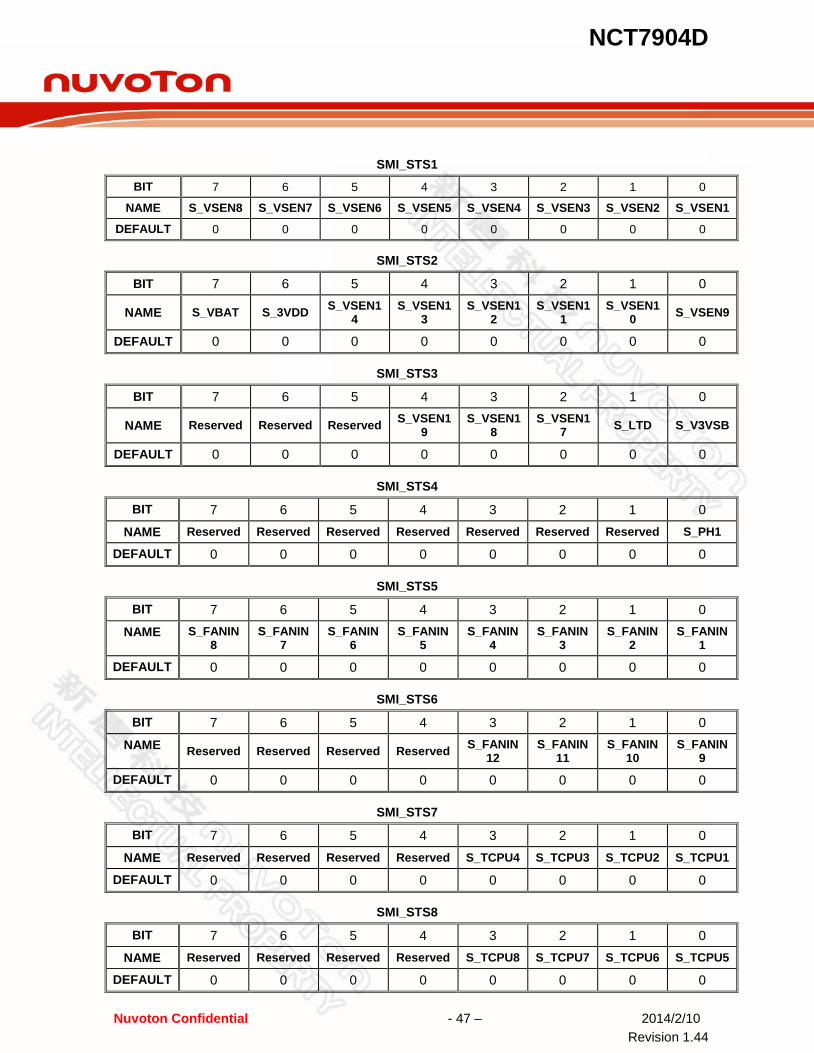
NCT7904D
Nuvoton Confidential - 47 – 2014/2/10 Revision 1.44
SMI_STS1
BIT 7 6 5 4 3 2 1 0
NAME S_VSEN8 S_VSEN7 S_VSEN6 S_VSEN5 S_VSEN4 S_VSEN3 S_VSEN2 S_VSEN1
DEFAULT 0 0 0 0 0 0 0 0
SMI_STS2
BIT 7 6 5 4 3 2 1 0
NAME S_VBAT S_3VDD S_VSEN14
S_VSEN13
S_VSEN12
S_VSEN11
S_VSEN10 S_VSEN9
DEFAULT 0 0 0 0 0 0 0 0
SMI_STS3
BIT 7 6 5 4 3 2 1 0
NAME Reserved Reserved Reserved S_VSEN19
S_VSEN18
S_VSEN17 S_LTD S_V3VSB
DEFAULT 0 0 0 0 0 0 0 0
SMI_STS4
BIT 7 6 5 4 3 2 1 0 NAME Reserved Reserved Reserved Reserved Reserved Reserved Reserved S_PH1
DEFAULT 0 0 0 0 0 0 0 0
SMI_STS5
BIT 7 6 5 4 3 2 1 0 NAME S_FANIN
8 S_FANIN
7 S_FANIN
6 S_FANIN
5 S_FANIN
4 S_FANIN
3 S_FANIN
2 S_FANIN
1
DEFAULT 0 0 0 0 0 0 0 0
SMI_STS6
BIT 7 6 5 4 3 2 1 0 NAME Reserved Reserved Reserved Reserved S_FANIN
12 S_FANIN
11 S_FANIN
10 S_FANIN
9
DEFAULT 0 0 0 0 0 0 0 0
SMI_STS7
BIT 7 6 5 4 3 2 1 0 NAME Reserved Reserved Reserved Reserved S_TCPU4 S_TCPU3 S_TCPU2 S_TCPU1
DEFAULT 0 0 0 0 0 0 0 0
SMI_STS8
BIT 7 6 5 4 3 2 1 0 NAME Reserved Reserved Reserved Reserved S_TCPU8 S_TCPU7 S_TCPU6 S_TCPU5
DEFAULT 0 0 0 0 0 0 0 0

NCT7904D
Nuvoton Confidential - 48 – 2014/2/10 Revision 1.44
SMI_STS9
BIT 7 6 5 4 3 2 1 0 NAME Reserved Reserved Reserved Reserved S_PCPU4 S_PCPU3 S_PCPU2 S_PCPU1
DEFAULT 0 0 0 0 0 0 0 0
SMI_STS10
BIT 7 6 5 4 3 2 1 0 NAME Reserved S_CHAS
SIS Reserved Reserved S_TART4 S_TART3 S_TART2 S_TART1
DEFAULT 0 0 0 0 0 0 0 0
*TART: When the Smart fan is driving the fan in full speed over 3 minutes, the TART will be asserted.
SMI Mask Register 7.1.21Location:
SMI_MSK1 - Bank 0 Address CBHEX SMI_MSK2 - Bank 0 Address CCHEX
SMI_MSK3 - Bank 0 Address CDHEX
SMI_MSK4 - Bank 0 Address CEHEX
SMI_MSK5 - Bank 0 Address CFHEX
SMI_MSK6 - Bank 0 Address D0HEX
SMI_MSK7 - Bank 0 Address D1HEX
SMI_MSK8 - Bank 0 Address D2HEX
SMI_MSK9 - Bank 0 Address D3HEX
SMI_MSK10 - Bank 0 Address D4HEX
Type: Read / Write Reset: Power On Reset RESETIN# with LOCK=0
SMI_MSK1
BIT 7 6 5 4 3 2 1 0 NAME M_VSEN
8 M_VSEN
7 M_VSEN
6 M_VSEN
5 M_VSEN
4 M_VSEN
3 M_VSEN
2 M_VSEN
1
DEFAULT 1 1 1 1 1 1 1 1
SMI_MSK2
BIT 7 6 5 4 3 2 1 0 NAME M_VBAT M_3VDD M_VSEN
14 M_VSEN
13 M_VSEN
12 M_VSEN
11 M_VSEN
10 M_VSEN
9
DEFAULT 1 1 1 1 1 1 1 1
SMI_MSK3
BIT 7 6 5 4 3 2 1 0 NAME Reserved Reserved Reserved M_VSEN
19 M_VSEN
18 M_VSEN
17 M_LTD M_V3VSB
DEFAULT 0 0 0 1 1 1 1 1

NCT7904D
Nuvoton Confidential - 49 – 2014/2/10 Revision 1.44
SMI_MSK4
BIT 7 6 5 4 3 2 1 0 NAME Reserved Reserved Reserved Reserved Reserved Reserved Reserved M_PH1
DEFAULT 0 0 0 0 0 0 0 1
SMI_MSK5
BIT 7 6 5 4 3 2 1 0 NAME M_FANIN
8 M_FANIN
7 M_FANIN
6 M_FANIN
5 M_FANIN
4 M_FANIN
3 M_FANIN
2 M_FANIN
1
DEFAULT 1 1 1 1 1 1 1 1
SMI_MSK6
BIT 7 6 5 4 3 2 1 0 NAME Reserved Reserved Reserved Reserved M_FANIN
12 M_FANIN
11 M_FANIN
10 M_FANIN
9
DEFAULT 0 0 0 0 1 1 1 1
SMI_MSK7
BIT 7 6 5 4 3 2 1 0 NAME Reserved Reserved Reserved Reserved M_TCPU
4 M_TCPU
3 M_TCPU
2 M_TCPU
1
DEFAULT 0 0 0 0 1 1 1 1
SMI_MSK8
BIT 7 6 5 4 3 2 1 0 NAME Reserved Reserved Reserved Reserved M_TCPU
8 M_TCPU
7 M_TCPU
6 M_TCPU
5
DEFAULT 0 0 0 0 1 1 1 1
SMI_MSK9
BIT 7 6 5 4 3 2 1 0 NAME Reserved Reserved Reserved Reserved M_PCPU
4 M_PCPU
3 M_PCPU
2 M_PCPU
1
DEFAULT 0 0 0 0 1 1 1 1
SMI_MSK10
BIT 7 6 5 4 3 2 1 0 NAME CLR_CH
ASSIS M_CHAS
SIS Reserved Reserved M_TART4 M_TART3 M_TART2 M_TART1
DEFAULT 0 1 0 0 1 1 1 1 CLR_CHASSIS is clear chassis event. When write 1 , the internal chassis event will be cleared. M_CHASSIS is mask chassis event. When set to 1 , the chassis SMI event will be masked.
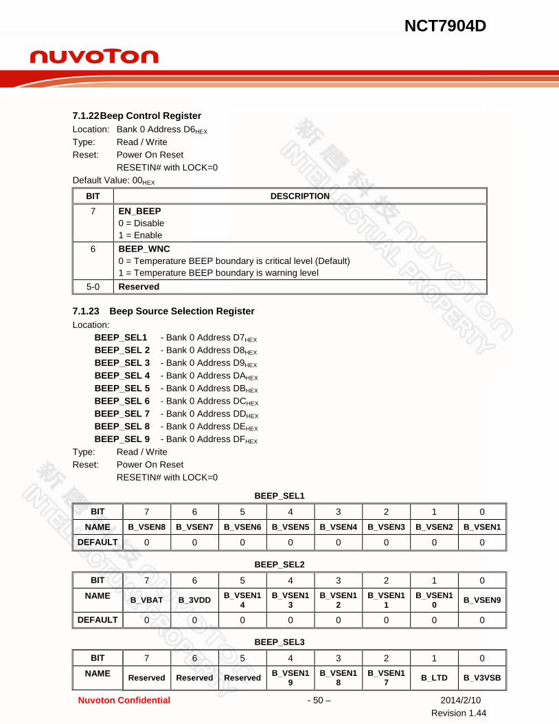
NCT7904D
Nuvoton Confidential - 50 – 2014/2/10 Revision 1.44
Beep Control Register 7.1.22Location: Bank 0 Address D6HEX Type: Read / Write Reset: Power On Reset RESETIN# with LOCK=0 Default Value: 00HEX
BIT DESCRIPTION
7 EN_BEEP 0 = Disable 1 = Enable
6 BEEP_WNC 0 = Temperature BEEP boundary is critical level (Default) 1 = Temperature BEEP boundary is warning level
5-0 Reserved
Beep Source Selection Register 7.1.23Location:
BEEP_SEL1 - Bank 0 Address D7HEX BEEP_SEL 2 - Bank 0 Address D8HEX
BEEP_SEL 3 - Bank 0 Address D9HEX
BEEP_SEL 4 - Bank 0 Address DAHEX
BEEP_SEL 5 - Bank 0 Address DBHEX
BEEP_SEL 6 - Bank 0 Address DCHEX
BEEP_SEL 7 - Bank 0 Address DDHEX
BEEP_SEL 8 - Bank 0 Address DEHEX
BEEP_SEL 9 - Bank 0 Address DFHEX
Type: Read / Write Reset: Power On Reset RESETIN# with LOCK=0
BEEP_SEL1
BIT 7 6 5 4 3 2 1 0 NAME B_VSEN8 B_VSEN7 B_VSEN6 B_VSEN5 B_VSEN4 B_VSEN3 B_VSEN2 B_VSEN1
DEFAULT 0 0 0 0 0 0 0 0
BEEP_SEL2
BIT 7 6 5 4 3 2 1 0 NAME B_VBAT B_3VDD B_VSEN1
4 B_VSEN1
3 B_VSEN1
2 B_VSEN1
1 B_VSEN1
0 B_VSEN9
DEFAULT 0 0 0 0 0 0 0 0
BEEP_SEL3
BIT 7 6 5 4 3 2 1 0 NAME Reserved Reserved Reserved B_VSEN1
9 B_VSEN1
8 B_VSEN1
7 B_LTD B_V3VSB

NCT7904D
Nuvoton Confidential - 51 – 2014/2/10 Revision 1.44
DEFAULT 0 0 0 0 0 0 0 0
BEEP_SEL4
BIT 7 6 5 4 3 2 1 0 NAME Reserved Reserved Reserved Reserved Reserved Reserved Reserved B_PH1
DEFAULT 0 0 0 0 0 0 0 0
BEEP_SEL5
BIT 7 6 5 4 3 2 1 0 NAME B_FANIN
8 B_FANIN
7 B_FANIN
6 B_FANIN
5 B_FANIN
4 B_FANIN
3 B_FANIN
2 B_FANIN
1
DEFAULT 0 0 0 0 0 0 0 0
BEEP_SEL6
BIT 7 6 5 4 3 2 1 0 NAME Reserved Reserved Reserved Reserved B_FANIN
12 B_FANIN
11 B_FANIN
10 B_FANIN
9
DEFAULT 0 0 0 0 0 0 0 0
BEEP_SEL7
BIT 7 6 5 4 3 2 1 0 NAME Reserved Reserved Reserved Reserved B_TCPU4 B_TCPU3 B_TCPU2 B_TCPU1
DEFAULT 0 0 0 0 0 0 0 0
BEEP_SEL8
BIT 7 6 5 4 3 2 1 0 NAME Reserved Reserved Reserved Reserved B_TCPU8 B_TCPU7 B_TCPU6 B_TCPU5
DEFAULT 0 0 0 0 0 0 0 0
BEEP_SEL9
BIT 7 6 5 4 3 2 1 0 NAME Reserved B_CHAS
SIS Reserved Reserved B_PCPU4 B_PCPU3 B_PCPU2 B_PCPU1
DEFAULT 0 0 0 0 0 0 0 0
Lock Watch Dog Register 7.1.24Location: Bank 0 Address E0HEX Type: Write Only Reset: Power On Reset Default Value: 00HEX
BIT DESCRIPTION
7-0 UNLOCK CODE Write 55HEX, Enables Soft Watch Dog Timer

NCT7904D
Nuvoton Confidential - 52 – 2014/2/10 Revision 1.44
Write AAHEX, Disables Soft Watch Dog Timer Write 33HEX, Enables Hard Watch Dog Timer Write CCHEX, Disables Hard Watch Dog Timer
Watch Dog Enable Register 7.1.25Location: Bank 0 Address E1HEX Type: Read Only Reset: Power On Reset Default Value: 00HEX
BIT DESCRIPTION
7-2 Reserved. 1 HARD
0 = Hard Watch Dog is disabled 1 = Hard Watch Dog is enabled
0 SOFT 0 = Soft Watch Dog is disabled 1 = Soft Watch Dog is enabled
Watch Dog Status Register 7.1.26Location: Bank 0 Address E2HEX Type: Read Only Reset: Power On Reset Default Value: 00HEX
BIT DESCRIPTION
7-4 Reserved
3-2 WDT_ST These 2 bits record last WDT stage for BIOS readout. The information is used to help BIOS to identify WDT timeout issuance
1 HARD_TO 1 = A hard timeout occurs. This bit will be cleared after reading
0 SOFT_TO 1 = A soft timeout occurs. This bit will be cleared after reading
Watch Dog Timer Register 7.1.27Location: Bank 0 Address E3HEX Type: Read / Write Reset: Power On Reset Default Value: 00HEX
BIT DESCRIPTION
7-0 WDT TIMER – Timeout timer To write 00HEX can disable the timer while in Hard Watch Dog Timer mode. To set Timeout Time for SOFT Watch Dog Timer, the unit is minute

NCT7904D
Nuvoton Confidential - 53 – 2014/2/10 Revision 1.44
GPIO Control Register 7.1.28Reset: Power On Reset RESETIN# with LOCK=0 GPIO G0 EN – GPIO Group 0 I/O Enable Control Register Location: Bank 0 Address E8HEX
Default Value: 60HEX
Type: Read / Write
BIT DESCRIPTION
7 Reserved
6-0 GPIO G0 EN – Select GPIOG-GPIOA I/O Enable. 0 = GPIOG-A are disable. 1 = GPIOG-A are enable.
GPIO G0 DIR – GPIO Group 0 I/O Direction Control Register Location: Bank 0 Address E9HEX
Default Value: 7FHEX
Type: Read / Write
BIT DESCRIPTION
7 Reserved 6-0 GPIO G0 DIR – Select GPIOG-GPIOA I/O Direction.
0 = GPIOG-A are programming as output pins. 1 = GPIOG-A are programming as input pins. (default)
GPIO G0 OUT – GPIO Group 0 Output Data Register Location: Bank 0 Address EAHEX
Default Value: 00HEX
Type: Read / Write
BIT DESCRIPTION
7-0 GPIO G0 OUT – Output GPIOG-GPIOA Data. For output ports, it needs to set GPIO_G0_EN register and the respective bits can be read/written and produced to pins.
GPIO G0 IN – GPIO Group 0 Input Data Register Location: Bank 0 Address EBHEX
Default Value: N.A. Type: Read Only
BIT DESCRIPTION
7-0 GPIO G0 IN – Input GPIOG-GPIOA Data. The respective bits can be read only from pins. Write accesses will be ignored.

NCT7904D
Nuvoton Confidential - 54 – 2014/2/10 Revision 1.44
GPIO G1 EN – GPIO Group 1 I/O Enable Control Register Location: Bank 0 Address ECHEX
Default Value: 00HEX
Type: Read / Write
BIT DESCRIPTION
7-4 Reserved 3-0 GPIO G1 EN – Select GPIO16-GPIO13 I/O Enable.
0 = GPIO16-13 are disable. 1 = GPIO16-13 are enable.
GPIO G1 DIR – GPIO Group 1 I/O Direction Control Register Location: Bank 0 Address EDHEX
Default Value: 0FHEX
Type: Read / Write
BIT DESCRIPTION
7-4 Reserved 3-0 GPIO G1 DIR – Select GPIO16-GPIO13 I/O Direction.
0 = GPIO16-13 are programming as output pins. 1 = GPIO16-13 are programming as input pins. (default)
GPIO G1 OUT – GPIO Group 1 Output Data Register Location: Bank 0 Address EEHEX
Default Value: 00HEX
Type: Read / Write
BIT DESCRIPTION
3-0 GPIO G1 OUT – Output GPIO16-GPIO13 Data. For output ports, it needs to set GPIO_G1_EN register and the respective bits can be read/written and produced to pins.
GPIO G1 IN – GPIO Group 1 Input Data Register Location: Bank 0 Address EFHEX
Default Value: N.A. Type: Read Only
BIT DESCRIPTION
3-0 GPIO G1 IN – Input GPIO16-GPIO13 Data. The respective bits can be read only from pins. Write accesses will be ignored.
PCH DTS Monitored Value Register 7.1.29Location: PCH_MAX - Bank 0 Address F0HEX
PCH_PCH - Bank 0 Address F1HEX
PCH_CPU_F - Bank 0 Address F2HEX
PCH_CPU_I - Bank 0 Address F3HEX
PCH_MCH - Bank 0 Address F4HEX
PCH_DIMM0 - Bank 0 Address F5HEX
PCH_DIMM1 - Bank 0 Address F6HEX
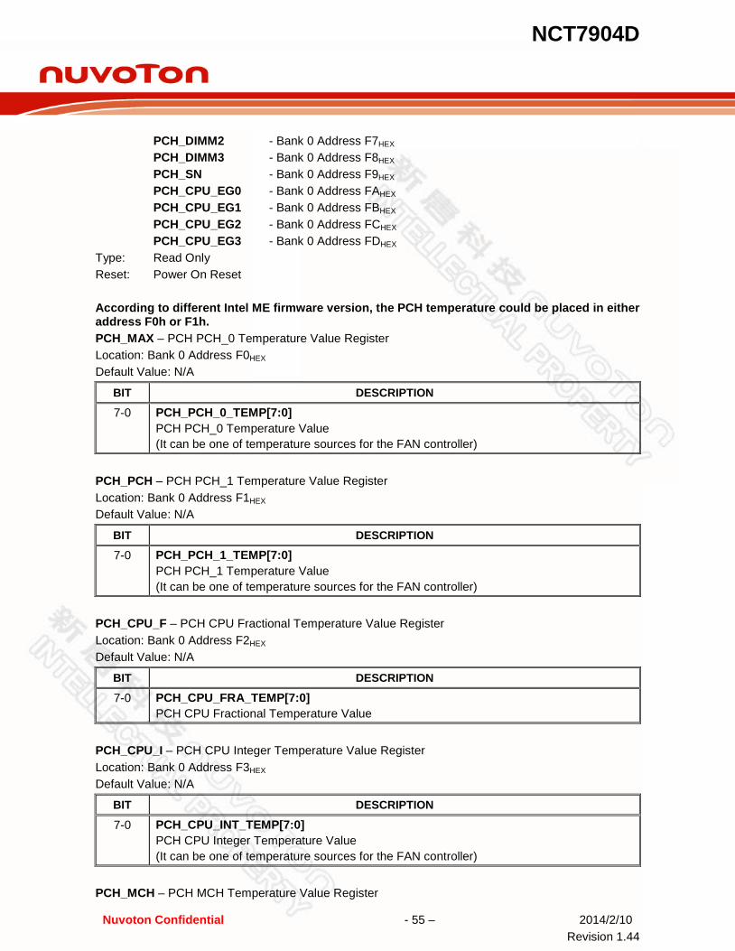
NCT7904D
Nuvoton Confidential - 55 – 2014/2/10 Revision 1.44
PCH_DIMM2 - Bank 0 Address F7HEX
PCH_DIMM3 - Bank 0 Address F8HEX
PCH_SN - Bank 0 Address F9HEX
PCH_CPU_EG0 - Bank 0 Address FAHEX
PCH_CPU_EG1 - Bank 0 Address FBHEX
PCH_CPU_EG2 - Bank 0 Address FCHEX
PCH_CPU_EG3 - Bank 0 Address FDHEX
Type: Read Only Reset: Power On Reset According to different Intel ME firmware version, the PCH temperature could be placed in either address F0h or F1h. PCH_MAX – PCH PCH_0 Temperature Value Register Location: Bank 0 Address F0HEX
Default Value: N/A
BIT DESCRIPTION
7-0 PCH_PCH_0_TEMP[7:0] PCH PCH_0 Temperature Value (It can be one of temperature sources for the FAN controller)
PCH_PCH – PCH PCH_1 Temperature Value Register Location: Bank 0 Address F1HEX
Default Value: N/A
BIT DESCRIPTION
7-0 PCH_PCH_1_TEMP[7:0] PCH PCH_1 Temperature Value (It can be one of temperature sources for the FAN controller)
PCH_CPU_F – PCH CPU Fractional Temperature Value Register Location: Bank 0 Address F2HEX
Default Value: N/A
BIT DESCRIPTION
7-0 PCH_CPU_FRA_TEMP[7:0] PCH CPU Fractional Temperature Value
PCH_CPU_I – PCH CPU Integer Temperature Value Register Location: Bank 0 Address F3HEX
Default Value: N/A
BIT DESCRIPTION
7-0 PCH_CPU_INT_TEMP[7:0] PCH CPU Integer Temperature Value (It can be one of temperature sources for the FAN controller)
PCH_MCH – PCH MCH Temperature Value Register
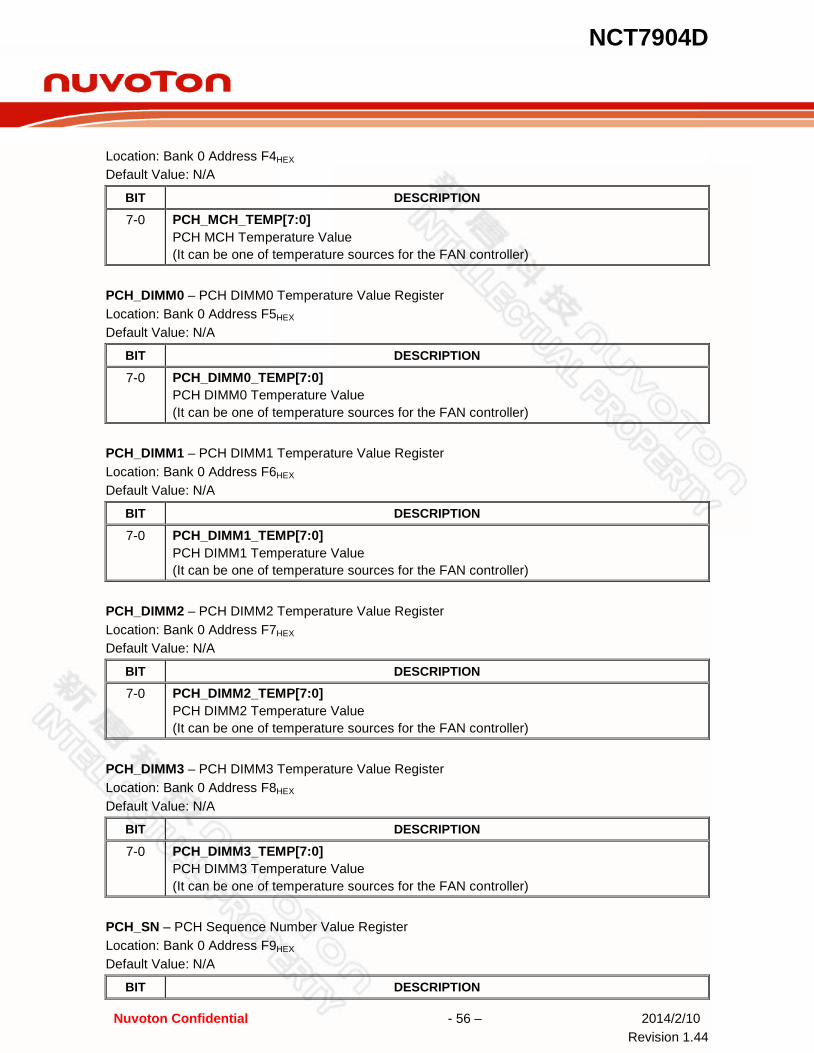
NCT7904D
Nuvoton Confidential - 56 – 2014/2/10 Revision 1.44
Location: Bank 0 Address F4HEX
Default Value: N/A
BIT DESCRIPTION
7-0 PCH_MCH_TEMP[7:0] PCH MCH Temperature Value (It can be one of temperature sources for the FAN controller)
PCH_DIMM0 – PCH DIMM0 Temperature Value Register Location: Bank 0 Address F5HEX
Default Value: N/A
BIT DESCRIPTION
7-0 PCH_DIMM0_TEMP[7:0] PCH DIMM0 Temperature Value (It can be one of temperature sources for the FAN controller)
PCH_DIMM1 – PCH DIMM1 Temperature Value Register Location: Bank 0 Address F6HEX
Default Value: N/A
BIT DESCRIPTION
7-0 PCH_DIMM1_TEMP[7:0] PCH DIMM1 Temperature Value (It can be one of temperature sources for the FAN controller)
PCH_DIMM2 – PCH DIMM2 Temperature Value Register Location: Bank 0 Address F7HEX
Default Value: N/A
BIT DESCRIPTION
7-0 PCH_DIMM2_TEMP[7:0] PCH DIMM2 Temperature Value (It can be one of temperature sources for the FAN controller)
PCH_DIMM3 – PCH DIMM3 Temperature Value Register Location: Bank 0 Address F8HEX
Default Value: N/A
BIT DESCRIPTION
7-0 PCH_DIMM3_TEMP[7:0] PCH DIMM3 Temperature Value (It can be one of temperature sources for the FAN controller)
PCH_SN – PCH Sequence Number Value Register Location: Bank 0 Address F9HEX
Default Value: N/A
BIT DESCRIPTION

NCT7904D
Nuvoton Confidential - 57 – 2014/2/10 Revision 1.44
BIT DESCRIPTION
7-0 PCH_SEQ_NUM[7:0] PCH Sequence Number Value
PCH_CPU_EG0 – PCH CPU Latest Energy Value Register Location: Bank 0 Address FAHEX
Default Value: N/A
BIT DESCRIPTION
7-0 PCH_CPU_ERG[7:0] PCH CPU Latest Energy Value
PCH_CPU_EG1 – PCH CPU Latest Energy Value Register Location: Bank 0 Address FBHEX
Default Value: N/A
BIT DESCRIPTION
7-0 PCH_CPU_ERG[15:8] PCH CPU Latest Energy Value
PCH_CPU_EG2 – PCH CPU Latest Energy Value Register Location: Bank 0 Address FCHEX
Default Value: N/A
BIT DESCRIPTION
7-0 PCH_CPU_ERG[23:16] PCH CPU Latest Energy Value
PCH_CPU_EG3 – PCH CPU Latest Energy Value Register Location: Bank 0 Address FDHEX
Default Value: N/A
BIT DESCRIPTION
7-0 PCH_CPU_ERG[31:24] PCH CPU Latest Energy Value
Bank Select Register 7.1.30Location: Bank 0, 1, 2, 3 Address FFHEX Type: Read / Write Reset: Power On Reset RESETIN# with LOCK=0 Default Value: 00HEX
BIT DESCRIPTION
7-3 Reserved. 2-0 BANK_SEL[2:0]
000BIN = Bank 0

NCT7904D
Nuvoton Confidential - 58 – 2014/2/10 Revision 1.44
BIT DESCRIPTION 001BIN = Bank 1 010BIN = Bank 2 011BIN = Bank 3 100BIN = Bank 4 101BIN ~ 111BIN = Reserved
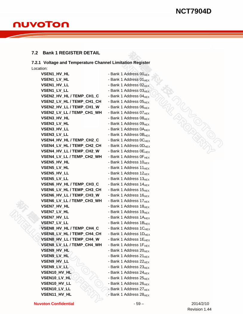
NCT7904D
Nuvoton Confidential - 59 – 2014/2/10 Revision 1.44
7.2 Bank 1 REGISTER DETAIL
Voltage and Temperature Channel Limitation Register 7.2.1Location:
VSEN1_HV_HL - Bank 1 Address 00HEX
VSEN1_LV_HL - Bank 1 Address 01HEX
VSEN1_HV_LL - Bank 1 Address 02HEX
VSEN1_LV_LL - Bank 1 Address 03HEX
VSEN2_HV_HL / TEMP_CH1_C - Bank 1 Address 04HEX
VSEN2_LV_HL / TEMP_CH1_CH - Bank 1 Address 05HEX
VSEN2_HV_LL / TEMP_CH1_W - Bank 1 Address 06HEX
VSEN2_LV_LL / TEMP_CH1_WH - Bank 1 Address 07HEX
VSEN3_HV_HL - Bank 1 Address 08HEX
VSEN3_LV_HL - Bank 1 Address 09HEX
VSEN3_HV_LL - Bank 1 Address 0AHEX
VSEN3_LV_LL - Bank 1 Address 0BHEX
VSEN4_HV_HL / TEMP_CH2_C - Bank 1 Address 0CHEX
VSEN4_LV_HL / TEMP_CH2_CH - Bank 1 Address 0DHEX
VSEN4_HV_LL / TEMP_CH2_W - Bank 1 Address 0EHEX
VSEN4_LV_LL / TEMP_CH2_WH - Bank 1 Address 0FHEX
VSEN5_HV_HL - Bank 1 Address 10HEX
VSEN5_LV_HL - Bank 1 Address 11HEX
VSEN5_HV_LL - Bank 1 Address 12HEX
VSEN5_LV_LL - Bank 1 Address 13HEX
VSEN6_HV_HL / TEMP_CH3_C - Bank 1 Address 14HEX
VSEN6_LV_HL / TEMP_CH3_CH - Bank 1 Address 15HEX
VSEN6_HV_LL / TEMP_CH3_W - Bank 1 Address 16HEX
VSEN6_LV_LL / TEMP_CH3_WH - Bank 1 Address 17HEX
VSEN7_HV_HL - Bank 1 Address 18HEX
VSEN7_LV_HL - Bank 1 Address 19HEX
VSEN7_HV_LL - Bank 1 Address 1AHEX
VSEN7_LV_LL - Bank 1 Address 1BHEX
VSEN8_HV_HL / TEMP_CH4_C - Bank 1 Address 1CHEX
VSEN8_LV_HL / TEMP_CH4_CH - Bank 1 Address 1DHEX
VSEN8_HV_LL / TEMP_CH4_W - Bank 1 Address 1EHEX
VSEN8_LV_LL / TEMP_CH4_WH - Bank 1 Address 1FHEX
VSEN9_HV_HL - Bank 1 Address 20HEX
VSEN9_LV_HL - Bank 1 Address 21HEX
VSEN9_HV_LL - Bank 1 Address 22HEX
VSEN9_LV_LL - Bank 1 Address 23HEX
VSEN10_HV_HL - Bank 1 Address 24HEX
VSEN10_LV_HL - Bank 1 Address 25HEX
VSEN10_HV_LL - Bank 1 Address 26HEX
VSEN10_LV_LL - Bank 1 Address 27HEX
VSEN11_HV_HL - Bank 1 Address 28HEX
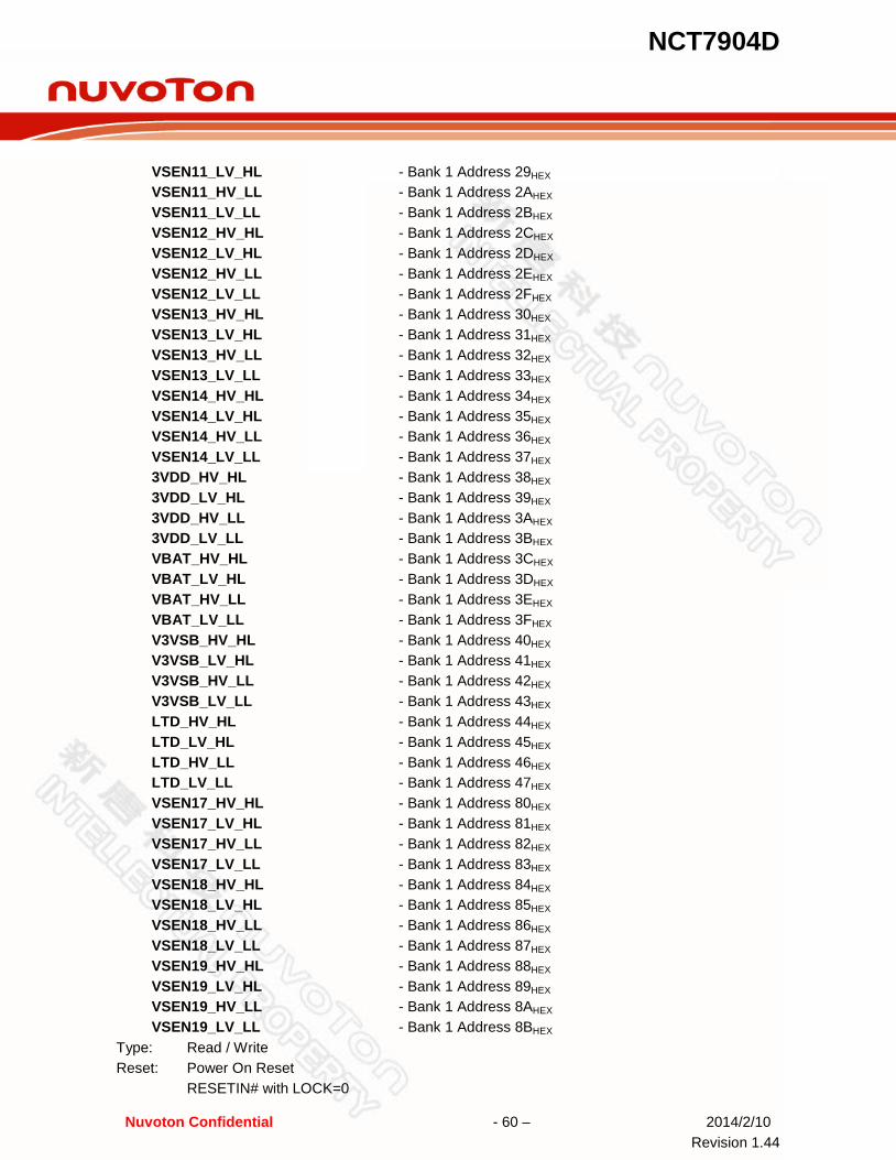
NCT7904D
Nuvoton Confidential - 60 – 2014/2/10 Revision 1.44
VSEN11_LV_HL - Bank 1 Address 29HEX
VSEN11_HV_LL - Bank 1 Address 2AHEX
VSEN11_LV_LL - Bank 1 Address 2BHEX
VSEN12_HV_HL - Bank 1 Address 2CHEX
VSEN12_LV_HL - Bank 1 Address 2DHEX
VSEN12_HV_LL - Bank 1 Address 2EHEX
VSEN12_LV_LL - Bank 1 Address 2FHEX
VSEN13_HV_HL - Bank 1 Address 30HEX
VSEN13_LV_HL - Bank 1 Address 31HEX
VSEN13_HV_LL - Bank 1 Address 32HEX
VSEN13_LV_LL - Bank 1 Address 33HEX
VSEN14_HV_HL - Bank 1 Address 34HEX
VSEN14_LV_HL - Bank 1 Address 35HEX
VSEN14_HV_LL - Bank 1 Address 36HEX
VSEN14_LV_LL - Bank 1 Address 37HEX
3VDD_HV_HL - Bank 1 Address 38HEX
3VDD_LV_HL - Bank 1 Address 39HEX
3VDD_HV_LL - Bank 1 Address 3AHEX
3VDD_LV_LL - Bank 1 Address 3BHEX
VBAT_HV_HL - Bank 1 Address 3CHEX
VBAT_LV_HL - Bank 1 Address 3DHEX
VBAT_HV_LL - Bank 1 Address 3EHEX
VBAT_LV_LL - Bank 1 Address 3FHEX
V3VSB_HV_HL - Bank 1 Address 40HEX
V3VSB_LV_HL - Bank 1 Address 41HEX
V3VSB_HV_LL - Bank 1 Address 42HEX
V3VSB_LV_LL - Bank 1 Address 43HEX
LTD_HV_HL - Bank 1 Address 44HEX
LTD_LV_HL - Bank 1 Address 45HEX
LTD_HV_LL - Bank 1 Address 46HEX
LTD_LV_LL - Bank 1 Address 47HEX
VSEN17_HV_HL - Bank 1 Address 80HEX
VSEN17_LV_HL - Bank 1 Address 81HEX
VSEN17_HV_LL - Bank 1 Address 82HEX
VSEN17_LV_LL - Bank 1 Address 83HEX
VSEN18_HV_HL - Bank 1 Address 84HEX
VSEN18_LV_HL - Bank 1 Address 85HEX
VSEN18_HV_LL - Bank 1 Address 86HEX
VSEN18_LV_LL - Bank 1 Address 87HEX
VSEN19_HV_HL - Bank 1 Address 88HEX
VSEN19_LV_HL - Bank 1 Address 89HEX
VSEN19_HV_LL - Bank 1 Address 8AHEX
VSEN19_LV_LL - Bank 1 Address 8BHEX
Type: Read / Write Reset: Power On Reset RESETIN# with LOCK=0
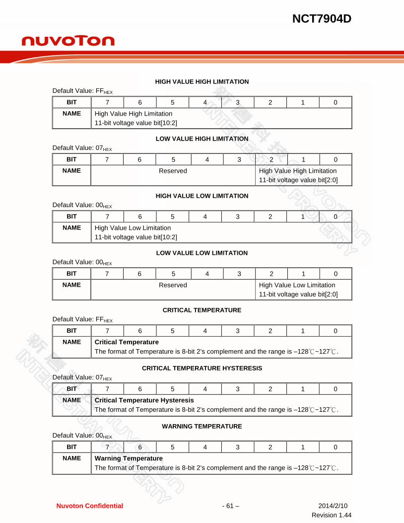
NCT7904D
Nuvoton Confidential - 61 – 2014/2/10 Revision 1.44
HIGH VALUE HIGH LIMITATION Default Value: FFHEX
BIT 7 6 5 4 3 2 1 0 NAME High Value High Limitation
11-bit voltage value bit[10:2]
LOW VALUE HIGH LIMITATION Default Value: 07HEX
BIT 7 6 5 4 3 2 1 0 NAME Reserved High Value High Limitation
11-bit voltage value bit[2:0]
HIGH VALUE LOW LIMITATION Default Value: 00HEX
BIT 7 6 5 4 3 2 1 0 NAME High Value Low Limitation
11-bit voltage value bit[10:2]
LOW VALUE LOW LIMITATION Default Value: 00HEX
BIT 7 6 5 4 3 2 1 0 NAME Reserved High Value Low Limitation
11-bit voltage value bit[2:0]
CRITICAL TEMPERATURE Default Value: FFHEX
BIT 7 6 5 4 3 2 1 0 NAME Critical Temperature
The format of Temperature is 8-bit 2’s complement and the range is –128℃~127℃.
CRITICAL TEMPERATURE HYSTERESIS Default Value: 07HEX
BIT 7 6 5 4 3 2 1 0
NAME Critical Temperature Hysteresis The format of Temperature is 8-bit 2’s complement and the range is –128℃~127℃.
WARNING TEMPERATURE Default Value: 00HEX
BIT 7 6 5 4 3 2 1 0 NAME Warning Temperature
The format of Temperature is 8-bit 2’s complement and the range is –128℃~127℃.

NCT7904D
Nuvoton Confidential - 62 – 2014/2/10 Revision 1.44
WARNING TEMPERATURE HYSTERESIS Default Value: 00HEX
BIT 7 6 5 4 3 2 1 0 NAME Warning Temperature Hysteresis
The format of Temperature is 8-bit 2’s complement and the range is –128℃~127℃.
PROCHOT Limitation Register 7.2.2Location: Bank 1 Address 50HEX
Type: Read / Write Reset: Power On Reset RESETIN# with LOCK=0 Default Value: FFHEX
BIT DESCRIPTION
7-0 P1_PROCHOT#_NV_HL[7:0] CPU1 PROCHOT# Numerator High Limitation
FAN Input Channel Limitation Register 7.2.3Location: FANIN1_HV_HL - Bank 1 Address 60HEX
FANIN1_LV_HL - Bank 1 Address 61HEX
FANIN2_HV_HL - Bank 1 Address 62HEX
FANIN2_LV_HL - Bank 1 Address 63HEX
FANIN3_HV_HL - Bank 1 Address 64HEX
FANIN3_LV_HL - Bank 1 Address 65HEX
FANIN4_HV_HL - Bank 1 Address 66HEX
FANIN4_LV_HL - Bank 1 Address 67HEX
FANIN5_HV_HL - Bank 1 Address 68HEX
FANIN5_LV_HL - Bank 1 Address 69HEX
FANIN6_HV_HL - Bank 1 Address 6AHEX
FANIN6_LV_HL - Bank 1 Address 6BHEX
FANIN7_HV_HL - Bank 1 Address 6CHEX
FANIN7_LV_HL - Bank 1 Address 6DHEX
FANIN8_HV_HL - Bank 1 Address 6EHEX
FANIN8_LV_HL - Bank 1 Address 6FHEX
FANIN9_HV_HL - Bank 1 Address 70HEX
FANIN9_LV_HL - Bank 1 Address 71HEX
FANIN10_HV_HL - Bank 1 Address 72HEX
FANIN10_LV_HL - Bank 1 Address 73HEX
FANIN11_HV_HL - Bank 1 Address 74HEX
FANIN11_LV_HL - Bank 1 Address 75HEX
FANIN12_HV_HL - Bank 1 Address 76HEX
FANIN12_LV_HL - Bank 1 Address 77HEX
Type: Read / Write Reset: Power On Reset RESETIN# with LOCK=0

NCT7904D
Nuvoton Confidential - 63 – 2014/2/10 Revision 1.44
FANIN HIGH VALUE HIGH LIMITATION
BIT 7 6 5 4 3 2 1 0 NAME Fan Input Count High Value High Limitation
13-bit voltage value bit[12:5]
FANIN LOW VALUE HIGH LIMITATION
BIT 7 6 5 4 3 2 1 0 NAME Reserved
Fan Input Count Low Value High Limitation 13-bit voltage value bit[4:0]
DTS Temperature Power Limitation Registers 7.2.4Location:
DTS_T_CPU1_C - Bank 1 Address 90HEX
DTS_T_CPU1_CH - Bank 1 Address 91HEX
DTS_T_CPU1_W - Bank 1 Address 92HEX
DTS_T_CPU1_WH - Bank 1 Address 93HEX
DTS_T_CPU2_C - Bank 1 Address 94HEX
DTS_T_CPU2_CH - Bank 1 Address 95HEX
DTS_T_CPU2_W - Bank 1 Address 96HEX
DTS_T_CPU2_WH - Bank 1 Address 97HEX
DTS_T_CPU3_C - Bank 1 Address 98HEX
DTS_T_CPU3_CH - Bank 1 Address 99HEX
DTS_T_CPU3_W - Bank 1 Address 9AHEX
DTS_T_CPU3_WH - Bank 1 Address 9BHEX
DTS_T_CPU4_C - Bank 1 Address 9CHEX
DTS_T_CPU4_CH - Bank 1 Address 9DHEX
DTS_T_CPU4_W - Bank 1 Address 9EHEX
DTS_T_CPU4_WH - Bank 1 Address 9FHEX
DTS_T_CPU5_C - Bank 1 Address A0HEX
DTS_T_CPU5_CH - Bank 1 Address A1HEX
DTS_T_CPU5_W - Bank 1 Address A2HEX
DTS_T_CPU5_WH - Bank 1 Address A3HEX
DTS_T_CPU6_C - Bank 1 Address A4HEX
DTS_T_CPU6_CH - Bank 1 Address A5HEX
DTS_T_CPU6_W - Bank 1 Address A6HEX
DTS_T_CPU6_WH - Bank 1 Address A7HEX
DTS_T_CPU7_C - Bank 1 Address A8HEX
DTS_T_CPU7_CH - Bank 1 Address A9HEX
DTS_T_CPU7_W - Bank 1 Address AAHEX
DTS_T_CPU7_WH - Bank 1 Address ABHEX
DTS_T_CPU8_C - Bank 1 Address ACHEX
DTS_T_CPU8_CH - Bank 1 Address ADEX
DTS_T_CPU8_W - Bank 1 Address AEHEX
DTS_T_CPU8_WH - Bank 1 Address AFHEX
DTS_P_CPU1_C - Bank 1 Address B0HEX
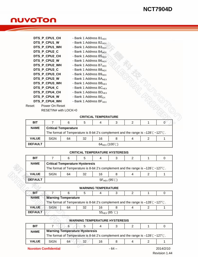
NCT7904D
Nuvoton Confidential - 64 – 2014/2/10 Revision 1.44
DTS_P_CPU1_CH - Bank 1 Address B1HEX
DTS_P_CPU1_W - Bank 1 Address B2HEX
DTS_P_CPU1_WH - Bank 1 Address B3HEX
DTS_P_CPU2_C - Bank 1 Address B4HEX
DTS_P_CPU2_CH - Bank 1 Address B5HEX
DTS_P_CPU2_W - Bank 1 Address B6HEX
DTS_P_CPU2_WH - Bank 1 Address B7HEX
DTS_P_CPU3_C - Bank 1 Address B8HEX
DTS_P_CPU3_CH - Bank 1 Address B9HEX
DTS_P_CPU3_W - Bank 1 Address BAHEX
DTS_P_CPU3_WH - Bank 1 Address BBHEX
DTS_P_CPU4_C - Bank 1 Address BCHEX
DTS_P_CPU4_CH - Bank 1 Address BDHEX
DTS_P_CPU4_W - Bank 1 Address BEEX
DTS_P_CPU4_WH - Bank 1 Address BFHEX
Reset: Power On Reset RESETIN# with LOCK=0
CRITICAL TEMPERATURE
BIT 7 6 5 4 3 2 1 0 NAME Critical Temperature
The format of Temperature is 8-bit 2’s complement and the range is –128℃~127℃.
VALUE SIGN 64 32 16 8 4 2 1 DEFAULT 64HEX (100℃)
CRITICAL TEMPERATURE HYSTERESIS
BIT 7 6 5 4 3 2 1 0 NAME Critical Temperature Hysteresis
The format of Temperature is 8-bit 2’s complement and the range is –128℃~127℃.
VALUE SIGN 64 32 16 8 4 2 1 DEFAULT 5FHEX (95℃)
WARNING TEMPERATURE BIT 7 6 5 4 3 2 1 0
NAME Warning Temperature The format of Temperature is 8-bit 2’s complement and the range is –128℃~127℃.
VALUE SIGN 64 32 16 8 4 2 1 DEFAULT 55HEX (85 ℃)
WARNING TEMPERATURE HYSTERESIS
BIT 7 6 5 4 3 2 1 0 NAME Warning Temperature Hysteresis
The format of Temperature is 8-bit 2’s complement and the range is –128℃~127℃.
VALUE SIGN 64 32 16 8 4 2 1
NCT7904D
Nuvoton Confidential - 65 – 2014/2/10 Revision 1.44
DEFAULT 50HEX (80 ℃)
PROCHOT Control Registers 7.2.5Location: Bank 1 Address D0HEX
Type: Read / Write Reset: Power On Reset RESETIN# with LOCK=0 Default Value: 4FHEX
BIT DESCRIPTION
7 Reserved 6 PH1_MD – Set the PROCHOT1# mode.
0 = Output mode 1 = Input mode (default)
5-4 PH1_FSEL – Set the PROCHOT1# sample period time. 00 = 22us (default) 01 = 44us 10 = 88us 11 = 176us
3-0 PH1_DC – Set the PROCHOT1# output duty cycle. 0000 = 1 sample time low 0001 = 2 sample times low 0010 = 3 sample times low 0011 = 4 sample times low 0100 = 5 sample times low 0101 = 6 sample times low 0110 = 7 sample times low 0111 = 8 sample times low 1000 = 9 sample times low 1001 = 10 sample times low 1010 = 11 sample times low 1011 = 12 sample times low 1100 = 13 sample times low 1101 = 14 sample times low 1110 = 15 sample times low 1111 = all low (default)

NCT7904D
Nuvoton Confidential - 66 – 2014/2/10 Revision 1.44
PROCHOT Source Selection Registers 7.2.6Location:
PH1_VT_ADC - Bank 1 Address D1HEX
PH1_DTS_T0 - Bank 1 Address D2HEX
PH1_DTS_T1 - Bank 1 Address D3HEX PH1_DTS_P - Bank 1 Address D4HEX
Type: Read / Write Reset: Power On Reset RESETIN# with LOCK=0 PH1_VT_ADC – P1_PROCHOT Temperature Select Register Location: Bank 1 Address D1HEX
Default Value: 20HEX
BIT DESCRIPTION
7-5 Reserved 4 PH1_LTD – Enable P1_PROCHOT# for LTD
0 = Disable 1 = Enable
3 PH1_VSEN89 – Enable P1_PROCHOT# for VSEN89 0 = Disable 1 = Enable
2 PH1_VSEN67 – Enable P1_PROCHOT# for VSEN67 0 = Disable 1 = Enable
1 PH1_VSEN45 – Enable P1_PROCHOT# for VSEN45 0 = Disable 1 = Enable
0 PH1_VSEN23 – Enable P1_PROCHOT# for VSEN23 0 = Disable 1 = Enable
PH1_DTS_T0 – P1_PROCHOT DTS Temperature 0 Select Register Location: Bank 1 Address D2HEX
Default Value: 00HEX
BIT DESCRIPTION
7-4 Reserved 3 PH1_TCPU4 – Enable P1_PROCHOT# for TCPU4
0 = Disable 1 = Enable
2 PH1_TCPU3 – Enable P1_PROCHOT# for TCPU3 0 = Disable 1 = Enable
1 PH1_TCPU2 – Enable P1_PROCHOT# for TCPU2 0 = Disable 1 = Enable
0 PH1_TCPU1 – Enable P1_PROCHOT# for TCPU1

NCT7904D
Nuvoton Confidential - 67 – 2014/2/10 Revision 1.44
BIT DESCRIPTION 0 = Disable 1 = Enable
PH1_DTS_T1 – P1_PROCHOT DTS Temperature 1 Select Register Location: Bank 1 Address D3HEX
Default Value: 00HEX
BIT DESCRIPTION
7-4 Reserved 3 PH1_TCPU8 – Enable P1_PROCHOT# for TCPU8
0 = Disable 1 = Enable
2 PH1_TCPU7 – Enable P1_PROCHOT# for TCPU7 0 = Disable 1 = Enable
1 PH1_TCPU6 – Enable P1_PROCHOT# for TCPU6 0 = Disable 1 = Enable
0 PH1_TCPU5 – Enable P1_PROCHOT# for TCPU5 0 = Disable 1 = Enable
PH1_DTS_P – P1_PROCHOT DTS Power Select Register Location: Bank 1 Address D4HEX
Default Value: 00HEX
BIT DESCRIPTION
7-4 Reserved 3 PH1_PCPU4 – Enable P1_PROCHOT# for PCPU4
0 = Disable 1 = Enable
2 PH1_PCPU3 – Enable P1_PROCHOT# for PCPU3 0 = Disable 1 = Enable
1 PH1_PCPU2 – Enable P1_PROCHOT# for PCPU2 0 = Disable 1 = Enable
0 PH1_PCPU1 – Enable P1_PROCHOT# for PCPU1 0 = Disable 1 = Enable
Voltage Fault Control Registers 7.2.7Location: Bank 1 Address D8HEX
Type: Read / Write Reset: Power On Reset RESETIN# with LOCK=0 Default Value: 00HEX

NCT7904D
Nuvoton Confidential - 68 – 2014/2/10 Revision 1.44
BIT DESCRIPTION
7 EN_VFAULT – Enable voltage fault function. 0 = Disable 1 = Enable
6-0 Reserved
Voltage Fault Source Selection Registers 7.2.8Location:
VF_SEL0 - Bank 1 Address D9HEX
VF_SEL1 - Bank 1 Address DAHEX
VF_SEL2 - Bank 1 Address DBHEX Type: Read / Write Reset: Power On Reset RESETIN# with LOCK=0 VF_SEL0 – Voltage Fault Select Register Location: Bank 1 Address D9HEX
Default Value: 00HEX
BIT DESCRIPTION
7 VF_VSEN8 – Enable VOLT_ALM# for VSEN8 0 = Disable 1 = Enable
6 VF_VSEN7 – Enable VOLT_ALM# for VSEN7 0 = Disable 1 = Enable
5 VF_VSEN6 – Enable VOLT_ALM# for VSEN6 0 = Disable 1 = Enable
4 VF_VSEN5 – Enable VOLT_ALM# for VSEN5 0 = Disable 1 = Enable
3 VF_VSEN4 – Enable VOLT_ALM# for VSEN4 0 = Disable 1 = Enable
2 VF_VSEN3 – Enable VOLT_ALM# for VSEN3 0 = Disable 1 = Enable
1 VF_VSEN2 – Enable VOLT_ALM# for VSEN2 0 = Disable 1 = Enable
0 VF_VSEN1 – Enable VOLT_ALM# for VSEN1 0 = Disable 1 = Enable

NCT7904D
Nuvoton Confidential - 69 – 2014/2/10 Revision 1.44
VF_SEL1 – Voltage Fault Select Register Location: Bank 1 Address DAHEX Default Value: 00HEX
BIT DESCRIPTION 7 VF_VBAT – Enable VOLT_ALM# for VBAT
0 = Disable 1 = Enable
6 VF_3VDD – Enable VOLT_ALM# for 3VDD 0 = Disable 1 = Enable
5 VF_VSEN14 – Enable VOLT_ALM# for VSEN14 0 = Disable 1 = Enable
4 VF_VSEN13 – Enable VOLT_ALM# for VSEN13 0 = Disable 1 = Enable
3 VF_VSEN12 – Enable VOLT_ALM# for VSEN12 0 = Disable 1 = Enable
2 VF_VSEN11 – Enable VOLT_ALM# for VSEN11 0 = Disable 1 = Enable
1 VF_VSEN10 – Enable VOLT_ALM# for VSEN10 0 = Disable 1 = Enable
0 VF_VSEN9 – Enable VOLT_ALM# for VSEN9 0 = Disable 1 = Enable
VF_SEL2 – Voltage Fault Select Register Location: Bank 1 Address DBHEX
Default Value: 00HEX
BIT DESCRIPTION
7-5 Reserved
4 VF_VSEN19 – Enable VOLT_ALM# for VSEN19 0 = Disable 1 = Enable
3 VF_VSEN18 – Enable VOLT_ALM# for VSEN18 0 = Disable 1 = Enable
2 VF_VSEN17 – Enable VOLT_ALM# for VSEN17 0 = Disable 1 = Enable
1 Reserved
0 VF_V3VSB – Enable VOLT_ALM# for 3VSB 0 = Disable 1 = Enable

NCT7904D
Nuvoton Confidential - 70 – 2014/2/10 Revision 1.44
Fan Fault Control Registers 7.2.9Location: Bank 1 Address DCHEX
Type: Read / Write Reset: Power On Reset Default Value: 00HEX
BIT DESCRIPTION
7 EN_FFAULT – Enable fan fault function. 0 = Disable 1 = Enable
6-0 Reserved
Fan Fault Source Selection Registers 7.2.10Location:
FF_SEL0 - Bank 1 Address DDHEX
FF_SEL1 - Bank 1 Address DEHEX
Type: Read / Write Reset: Power On Reset RESETIN# with LOCK=0 FF_SEL0 – Fan Fault Select Register Location: Bank 1 Address DDHEX
Default Value: 00HEX
BIT DESCRIPTION 7 FF_FANIN8 – Enable FAN_ALM# for FANIN8
0 = Disable 1 = Enable
6 FF_FANIN7 – Enable FAN_ALM# for FANIN7 0 = Disable 1 = Enable
5 FF_FANIN6 – Enable FAN_ALM# for FANIN6 0 = Disable 1 = Enable
4 FF_FANIN5 – Enable FAN_ALM# for FANIN5 0 = Disable 1 = Enable
3 FF_FANIN4 – Enable FAN_ALM# for FANIN4 0 = Disable 1 = Enable
2 FF_FANIN3 – Enable FAN_ALM# for FANIN3 0 = Disable 1 = Enable
1 FF_FANIN2 – Enable FAN_ALM# for FANIN2 0 = Disable 1 = Enable
0 FF_FANIN1 – Enable FAN_ALM# for FANIN1 0 = Disable
NCT7904D
Nuvoton Confidential - 71 – 2014/2/10 Revision 1.44
BIT DESCRIPTION 1 = Enable
FF_SEL1 – Fan Fault Select Register Location: Bank 1 Address DEHEX
Default Value: 00HEX
BIT DESCRIPTION
7-4 Reserved
3 FF_FANIN12 – Enable FAN_ALM# for FANIN12 0 = Disable 1 = Enable
2 FF_FANIN11 – Enable FAN_ALM# for FANIN11 0 = Disable 1 = Enable
1 FF_FANIN10 – Enable FAN_ALM# for FANIN10 0 = Disable 1 = Enable
0 FF_FANIN9 – Enable FAN_ALM# for FANIN9 0 = Disable 1 = Enable
Temperature Fault Control Registers 7.2.11Location: Bank 1 Address E0HEX
Type: Read / Write Reset: Power On Reset RESETIN# with LOCK=0 Default Value: 00HEX
BIT DESCRIPTION
7 EN_TFAULT – Enable temperature fault function. 0 = Disable (Default) 1 = Enable
6 TF_WNC 0 = Temperature fault boundary is critical level (Default) 1 = Temperature fault boundary is warning level
5-0 Reserved.
Temperature Fault Source Selection Registers 7.2.12Location:
TF_SEL0 - Bank 1 Address E1HEX
TF_SEL1 - Bank 1 Address E2HEX
TF_SEL2 - Bank 1 Address E3HEX
Type: Read / Write Reset: Power On Reset RESETIN# with LOCK=0

NCT7904D
Nuvoton Confidential - 72 – 2014/2/10 Revision 1.44
TF_SEL0 – Temperature Fault Select Register Location: Bank 1 Address E1HEX
Default Value: 00HEX
BIT DESCRIPTION
7-5 Reserved
4 TF_LTD – Enable TEMP_ALM# for LTD 0 = Disable 1 = Enable
3 TF_VSEN89 – Enable TEMP_ALM# for VSEN89 0 = Disable 1 = Enable
2 TF_VSEN67 – Enable TEMP_ALM# for VSEN67 0 = Disable 1 = Enable
1 TF_VSEN45 – Enable TEMP_ALM# for VSEN45 0 = Disable 1 = Enable
0 TF_VSEN23 – Enable TEMP_ALM# for VSEN23 0 = Disable 1 = Enable
TF_SEL1 – Temperature Fault Select Register Location: Bank 1 Address E2HEX
Default Value: 00HEX
BIT DESCRIPTION
7-4 Reserved 3 TF_TCPU4 – Enable TEMP_ALM# for TCPU4
0 = Disable 1 = Enable
2 TF_TCPU3 – Enable TEMP_ALM# for TCPU3 0 = Disable 1 = Enable
1 TF_TCPU2 – Enable TEMP_ALM# for TCPU2 0 = Disable 1 = Enable
0 TF_TCPU1 – Enable TEMP_ALM# for TCPU1 0 = Disable 1 = Enable
TF_SEL2 – Temperature Fault Select Register Location: Bank 1 Address E3HEX
Default Value: 00HEX
BIT DESCRIPTION
7-4 Reserved 3 TF_TCPU8 – Enable TEMP_ALM# for TCPU8
NCT7904D
Nuvoton Confidential - 73 – 2014/2/10 Revision 1.44
BIT DESCRIPTION 0 = Disable 1 = Enable
2 TF_TCPU7 – Enable TEMP_ALM# for TCPU7 0 = Disable 1 = Enable
1 TF_TCPU6 – Enable TEMP_ALM# for TCPU6 0 = Disable 1 = Enable
0 TF_TCPU5 – Enable TEMP_ALM# for TCPU5 0 = Disable 1 = Enable
THERMTRIP Control and Status Register 7.2.13Location: Bank 1 Address E8HEX
Default Value: 00HEX
Type: Read / Write Reset: Power On Reset RESETIN# with LOCK=0
BIT DESCRIPTION
7-3 Reserved.
2 CLR_THRM – Clear the thermal trip status. If write 1, to clear thermal trip status.
1 EN_THRM – Enable thermal trip event. 0 = Disable 1 = Enable
0
THRM_STS – Thermal trip event status. (Read Only) (Power by VBAT) 0 = Thermal trip event not occurred or be cleared. 1 = Thermal trip event occurred. (It will always be shown no matter what EN_THRM is)
NCT7904D
Nuvoton Confidential - 74 – 2014/2/10 Revision 1.44
7.3 Bank 2 REGISTER DETAIL
PECI Function Enable Register (PFE) 7.3.1Location: PFE - Bank 2 Address 00HEX Type: Read / Write Reset: Power On Reset RESETIN# with LOCK=0
PFE
BIT 7 6 5 4 3 2 1 0 NAME PECI_En Reserved Manual_En BiasRTH_En GetPower_En
DEFAULT 18HEX
BIT DESCRIPTION
7 Enable PECI Host Function. (PECI_En) 6-3 Reserved
2 Enable PECI Manual Mode Transaction (Manual_En) Fill in command content into PMMC and PMMWD registers defined in 7.3.8 and 7.3.9 section before enable this bit.
1
Enable function of weighting “Count” retrieved from GetTemp() to form CPU temperature 0BIN => Disable ( It means that Temperature = “Count” ) 1BIN => Enable ( It means that Temperature = “Count” * Scale, Scale is defined by Scale_Sel[2:0] in Bank2 Index03)
0
Get Power Function (GetPower_En) This function can routinely return the total energy consumed by the processor. 0BIN = Disable get CPU Power Function. 1BIN = Enable get CPU Power Function.
PECI Timing Configure Register (PTC) 7.3.2Location: PTC - Bank 2 Address 01HEX Type: Read / Write Reset: Power On Reset RESETIN# with LOCK=0
PTC
BIT 7 6 5 4 3 2 1 0 NAME RtHigher Clamp ATR Reserved
DEFAULT 01HEX
BIT DESCRIPTION

NCT7904D
Nuvoton Confidential - 75 – 2014/2/10 Revision 1.44
BIT DESCRIPTION
7
Return Higher Temperature between Doamin0 and domain1.(RtHigher) 0BIN = The temperature of each agent is returned from domain 0 or domain 1.
It depends on control register Bit[3:0] in Bank 2 Address 03HEX.
1BIN = Return the higher temperature between domain 0 and domain 1
6 PECI clamping function to filter the unreasonable DTS “count” value. (Clamp) 0 = DTS values are fully transparent. 1 = DTS values are clamped in -128 ~ 0.
5-4
Adjust Transaction Tbit Rate. (ATR)
CLKIN 14.318MHz 33MHz 48MHz
00BIN Tbit = 1.1us Tbit = 0.5us Tbit = 0.5us
01BIN Tbit = 2.2us Tbit = 1us Tbit = 1us
10BIN Tbit = 4.5us Tbit = 2us Tbit = 2us
11BIN Tbit = 8.9us Tbit = 4us Tbit = 4us
3-0 Reserved
PECI Agent and Domain Configure Register (PADC) 7.3.3Location: PADC - Bank 2 Address 02HEX Type: Read / Write Reset: Power On Reset RESETIN# with LOCK=0
PADC
BIT 7 6 5 4 3 2 1 0 NAME En_Agt[3:0] Dmn1_Agt[3:0]
DEFAULT 00HEX
BIT DESCRIPTION
7-4 Assign which agent will be approached by PECI host [Bit7] = CPU agent 3 [Bit6] = CPU agent 2 [Bit5] = CPU agent 1 [Bit4] = CPU agent 0
3-0 Indicate which agent equips with domain1. [Bit3] = Agent 3 with / without Domain1 [Bit2] = Agent 2 with / without Domain1 [Bit1] = Agent 1 with / without Domain1 [Bit0] = Agent 0 with / without Domain1

NCT7904D
Nuvoton Confidential - 76 – 2014/2/10 Revision 1.44
PECI Relative Temperature Scale Register (PRTS) 7.3.4Location: PRTS - Bank 2 Address 03HEX Type: Read / Write Reset: Power On Reset RESETIN# with LOCK=0
PRTS
BIT 7 6 5 4 3 2 1 0 NAME Reserved Scale_Sel[2:0] RtDmn_Agt[3:0]
DEFAULT 40HEX
BIT DESCRIPTION
7 Reserved
6-4
Weighting “count” to form temperature. It is available only while BIASRTH (Bank 2 Address 00HEX Bit[1]=1) is asserted, Through this, the final Temperature = “count” * Scale_Sel[2:0]. 000BIN = 0.78125 001BIN = 0.84375 010BIN = 0.90625 011BIN = 0.96875 100BIN = 1.03125 101BIN = 1.09375 110BIN = 1.15625 111BIN = 1.21875
3-0
Agent 3 – Agent 0 always return relative temperature in ARTR registers defined by 7.3.11. These bits specify that these relative temperatures are come from domain 0 or domain1. However this configuration is available only while RtHigher (Bank 2 Address 01HEX Bit[7]) is de-asserted. [bit3] = 0 / 1 => Agent3 will return the relative temperature from domain 0 / domain 1. [bit2] = 0 / 1 => Agent2 will return the relative temperature from domain 0 / domain 1. [bit1] = 0 / 1 => Agent1 will return the relative temperature from domain 0 / domain 1. [bit0] = 0 / 1 => Agent0 will return the relative temperature from domain 0 / domain 1.
DTS Power Source Control Register 7.3.5Location: Bank 2 Address 04HEX
Default Value: 01HEX
Type: Read / Write Reset: Power On Reset RESETIN# with LOCK=0
DPSC
BIT 7 6 5 4 3 2 1 0

NCT7904D
Nuvoton Confidential - 77 – 2014/2/10 Revision 1.44
NAME Reserved DTS_SRC_SEL T_RTA_EN DEFAULT 01HEX
BIT DESCRIPTION
7-3 Reserved. 2-1 DTS_SRC_SEL – DTS Source Selection
00 = All from PECI 01 = All from Host (LSN_EN must be disable) 10 = Reserved 11 = Temperature from PECI and Power from Host (LSN_EN must be enable)
0 T_RTA_EN – PECI Temperature Running Time Average Enable 0 = Disable 1 = Enable (Default)
TBit Width Register ( TBW ) 7.3.6Location: Bank 2 Address 05HEX
Type: Read Reset: Power On Reset RESETIN# with LOCK=0
TBW
BIT 7 6 5 4 3 2 1 0 NAME LSN_RST_CNT[6:0]
DEFAULT 00HEX
BIT DESCRIPTION
7-0 Record TBit time in PECI Listening mode. The allowable lowest PECI transaction speed is 125Kz.
PECI Listening Mode Configuration Register ( PLMC ) 7.3.7Location: Bank 2 Address 06HEX
Type: Read / Write Reset: Power On Reset RESETIN# with LOCK=0
TBW
BIT 7 6 5 4 3 2 1 0 NAME Reserved LSN_CMD_ERR Reserved LSN_EN LSN_TBIT_LW[1:0]
DEFAULT 01HEX
BIT DESCRIPTION
7-5 Reserved 4 LSN_CMD_ERR: Indicator for command error while PECI listening mode is active

NCT7904D
Nuvoton Confidential - 78 – 2014/2/10 Revision 1.44
3 Reserved 2 LSN_EN: Enable PECI listening mode
1-0 LSN_TBIT_LW: Idle state period selection 00b = 2-TBit 01b = 3-TBit 10b = 4-TBit 11b = 5-TBit
PECI VTT Power Detect Configuration Register ( PVCR ) 7.3.8Location: Bank 2 Address 07HEX
Type: Read / Write Reset: Power On Reset RESETIN# with LOCK=0
TBW
BIT 7 6 5 4 3 2 1 0 NAME VTT_OK Reserved VTT_CRC VTT_CLR VTT_INIT_STS
DEFAULT 03HEX
BIT DESCRIPTION
7 VTT_OK : VTT power OK indicator. (read only) ‘0’ : VTT is not OK. ‘1’ : VTT is OK.
6-3 Reserved 2 VTT_CRC : CRC input source selection
‘0’ : The input source of CRC is purely from PECI physical bus ‘1’ : The input source of CRC comes from host’s internal write-out data and PECI physical bus
1 VTT_CLR : Retention control for absolute temperature data ‘0’ : Keep last data while VTT is loss ‘1’ : Clear absolute temperature data to default value while VTT is loss
0 VTT_INIT_STS : PECI transaction control while VTT is shut off ‘0’ : PECI transaction never stop even though VTT is loss ‘1’ : Suspend PECI transaction while VTT is power loss
PECI Agent Tbase Temperature Register (PATB) 7.3.9Location:
PATB 0 - Bank 2 Address 08HEX
PATB 1 - Bank 2 Address 09HEX
PATB 2 - Bank 2 Address 0AHEX
PATB 3 - Bank 2 Address 0BHEX
Type: Read / Write Reset: Power On Reset RESETIN# with LOCK=0
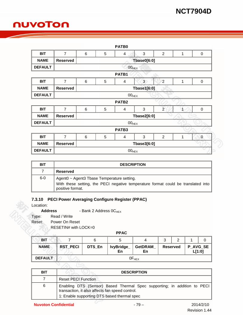
NCT7904D
Nuvoton Confidential - 79 – 2014/2/10 Revision 1.44
PATB0
BIT 7 6 5 4 3 2 1 0 NAME Reserved Tbase0[6:0]
DEFAULT 00HEX
PATB1
BIT 7 6 5 4 3 2 1 0 NAME Reserved Tbase1[6:0]
DEFAULT 00HEX
PATB2
BIT 7 6 5 4 3 2 1 0 NAME Reserved Tbase2[6:0]
DEFAULT 00HEX
PATB3
BIT 7 6 5 4 3 2 1 0 NAME Reserved Tbase3[6:0]
DEFAULT 00HEX
BIT DESCRIPTION
7 Reserved 6-0 Agent0 ~ Agent3 Tbase Temperature setting.
With these setting, the PECI negative temperature format could be translated into positive format.
PECI Power Averaging Configure Register (PPAC) 7.3.10Location:
Address - Bank 2 Address 0CHEX
Type: Read / Write Reset: Power On Reset RESETIN# with LOCK=0
PPAC
BIT 7 6 5 4 3 2 1 0 NAME RST_PECI DTS_En IvyBridge_
En GetDRAM_
En Reserved P_AVG_SE
L[1:0] DEFAULT 0FHEX
BIT DESCRIPTION
7 Reset PECI Function 6 Enabling DTS (Sensor) Based Thermal Spec supporting; in addition to PECI
transaction, it also affects fan speed control. 1: Enable supporting DTS based thermal spec
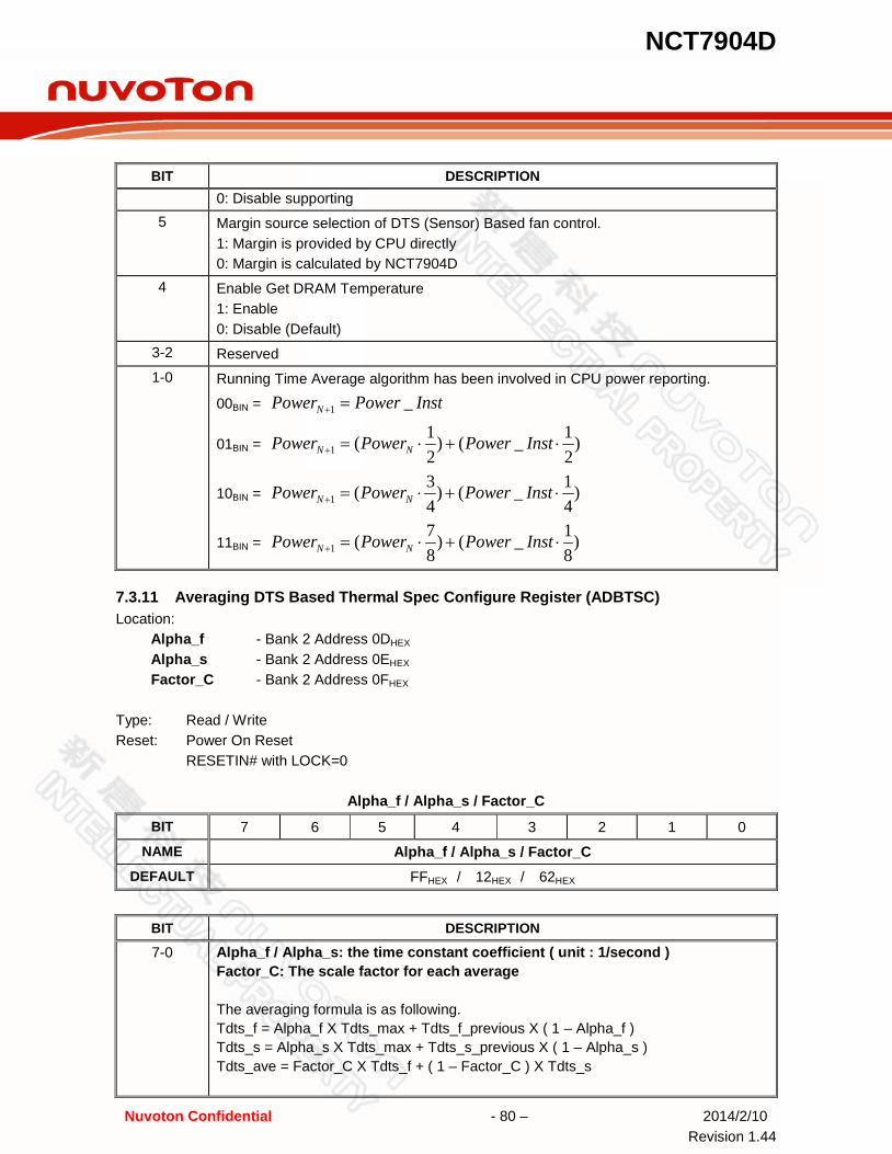
NCT7904D
Nuvoton Confidential - 80 – 2014/2/10 Revision 1.44
BIT DESCRIPTION 0: Disable supporting
5 Margin source selection of DTS (Sensor) Based fan control. 1: Margin is provided by CPU directly 0: Margin is calculated by NCT7904D
4 Enable Get DRAM Temperature 1: Enable 0: Disable (Default)
3-2 Reserved 1-0 Running Time Average algorithm has been involved in CPU power reporting.
00BIN = InstPowerPowerN _1 =+
01BIN = )21_()
21(1 ⋅+⋅=+ InstPowerPowerPower NN
10BIN = )41_()
43(1 ⋅+⋅=+ InstPowerPowerPower NN
11BIN = )81_()
87(1 ⋅+⋅=+ InstPowerPowerPower NN
Averaging DTS Based Thermal Spec Configure Register (ADBTSC) 7.3.11Location:
Alpha_f - Bank 2 Address 0DHEX
Alpha_s - Bank 2 Address 0EHEX
Factor_C - Bank 2 Address 0FHEX
Type: Read / Write Reset: Power On Reset RESETIN# with LOCK=0
Alpha_f / Alpha_s / Factor_C
BIT 7 6 5 4 3 2 1 0 NAME Alpha_f / Alpha_s / Factor_C
DEFAULT FFHEX / 12HEX / 62HEX
BIT DESCRIPTION
7-0 Alpha_f / Alpha_s: the time constant coefficient ( unit : 1/second ) Factor_C: The scale factor for each average The averaging formula is as following. Tdts_f = Alpha_f X Tdts_max + Tdts_f_previous X ( 1 – Alpha_f ) Tdts_s = Alpha_s X Tdts_max + Tdts_s_previous X ( 1 – Alpha_s ) Tdts_ave = Factor_C X Tdts_f + ( 1 – Factor_C ) X Tdts_s
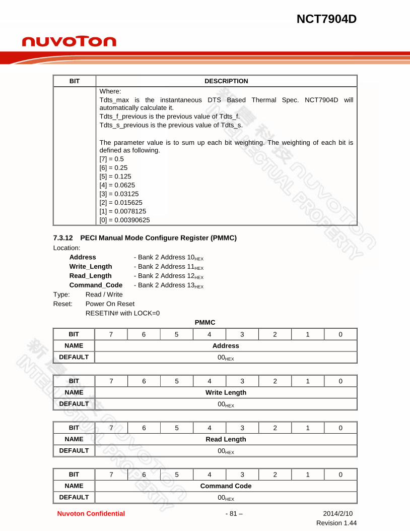
NCT7904D
Nuvoton Confidential - 81 – 2014/2/10 Revision 1.44
BIT DESCRIPTION Where: Tdts_max is the instantaneous DTS Based Thermal Spec. NCT7904D will automatically calculate it. Tdts_f_previous is the previous value of Tdts_f. Tdts_s_previous is the previous value of Tdts_s. The parameter value is to sum up each bit weighting. The weighting of each bit is defined as following. [7] = 0.5 [6] = 0.25 [5] = 0.125 [4] = 0.0625 [3] = 0.03125 [2] = 0.015625 [1] = 0.0078125 [0] = 0.00390625
PECI Manual Mode Configure Register (PMMC) 7.3.12Location:
Address - Bank 2 Address 10HEX
Write_Length - Bank 2 Address 11HEX
Read_Length - Bank 2 Address 12HEX
Command_Code - Bank 2 Address 13HEX
Type: Read / Write Reset: Power On Reset RESETIN# with LOCK=0
PMMC
BIT 7 6 5 4 3 2 1 0 NAME Address
DEFAULT 00HEX
BIT 7 6 5 4 3 2 1 0 NAME Write Length
DEFAULT 00HEX
BIT 7 6 5 4 3 2 1 0 NAME Read Length
DEFAULT 00HEX
BIT 7 6 5 4 3 2 1 0 NAME Command Code
DEFAULT 00HEX
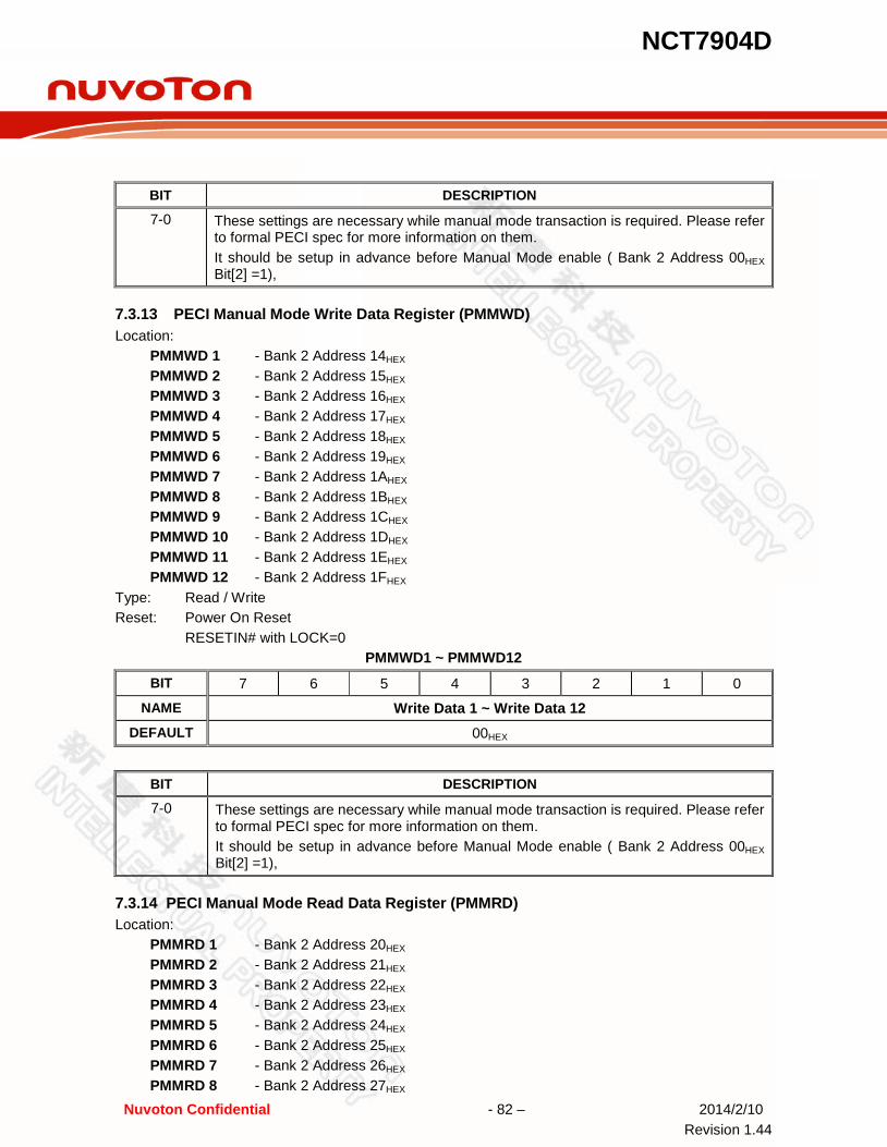
NCT7904D
Nuvoton Confidential - 82 – 2014/2/10 Revision 1.44
BIT DESCRIPTION
7-0 These settings are necessary while manual mode transaction is required. Please refer to formal PECI spec for more information on them. It should be setup in advance before Manual Mode enable ( Bank 2 Address 00HEX Bit[2] =1),
PECI Manual Mode Write Data Register (PMMWD) 7.3.13Location:
PMMWD 1 - Bank 2 Address 14HEX
PMMWD 2 - Bank 2 Address 15HEX
PMMWD 3 - Bank 2 Address 16HEX
PMMWD 4 - Bank 2 Address 17HEX
PMMWD 5 - Bank 2 Address 18HEX
PMMWD 6 - Bank 2 Address 19HEX
PMMWD 7 - Bank 2 Address 1AHEX
PMMWD 8 - Bank 2 Address 1BHEX
PMMWD 9 - Bank 2 Address 1CHEX
PMMWD 10 - Bank 2 Address 1DHEX
PMMWD 11 - Bank 2 Address 1EHEX
PMMWD 12 - Bank 2 Address 1FHEX
Type: Read / Write Reset: Power On Reset RESETIN# with LOCK=0
PMMWD1 ~ PMMWD12
BIT 7 6 5 4 3 2 1 0
NAME Write Data 1 ~ Write Data 12 DEFAULT 00HEX
BIT DESCRIPTION
7-0 These settings are necessary while manual mode transaction is required. Please refer to formal PECI spec for more information on them. It should be setup in advance before Manual Mode enable ( Bank 2 Address 00HEX Bit[2] =1),
PECI Manual Mode Read Data Register (PMMRD) 7.3.14Location:
PMMRD 1 - Bank 2 Address 20HEX
PMMRD 2 - Bank 2 Address 21HEX
PMMRD 3 - Bank 2 Address 22HEX
PMMRD 4 - Bank 2 Address 23HEX
PMMRD 5 - Bank 2 Address 24HEX
PMMRD 6 - Bank 2 Address 25HEX
PMMRD 7 - Bank 2 Address 26HEX
PMMRD 8 - Bank 2 Address 27HEX

NCT7904D
Nuvoton Confidential - 83 – 2014/2/10 Revision 1.44
PMMRD 9 - Bank 2 Address 28HEX
Type: Read Only Reset: Power On Reset
PMMRD1 ~ PMMRD9
BIT 7 6 5 4 3 2 1 0
NAME Read Data 1 ~ Read Data 9 DEFAULT 00HEX
BIT DESCRIPTION
7-0 These data are meaningful just after manual mode transaction is finished. Please refer to formal PECI spec for more information on them.
PECI Manual Mode Support Command and Data
Command Bank 2
Address CR 10HEX
Write Length CR 11HEX
Read Length CR 12HEX
Command Code CR 13HEX
Ping
30/ 31/ 32/ 33
00 00 Get DIB 01 08 F7
Get Temp 01 02 01 PCIRd30 06 02 / 03 / 05 61 PCIWr30 08 / 09 / 0B 01 65
PCIRdLocal30 05 02 / 03 / 05 E1 PCIWrLocal30 07 / 08 / 0A 01 E5
PKGRd30 05 02 / 03 / 05 A1 PKGWr30 07 / 08 / 0A 01 A5
IAMSRRd30 05 02 / 03 / 05 / 09 B1 IAMSRWr30 07 / 08 / 0A / 0E 01 B5
PECI Manual Mode Read Data Table
Command PCI Rd30
PCI Wr30
PCIRd Local3
0
PCIWr Local30
PKG Rd30
PKG Wr30
IAMSR Rd30
IAMSR Wr30
GetDIB GetTemp
Command Code
61 65 E1 E5 A1 A5 B1 B5 F7 01
RdData 1 CR 20HEX
Ccode Ccode Ccode Ccode Ccode Ccode Ccode Ccode * *
RdData 2 CR 21HEX
* * * * * * Data
LSB_1 *
Device Info
*
RdData 3 CR 22HEX
* * * * * * Data
LSB_2 *
Revision Number
*
RdData 4 * * * * * * Data * Reserved *
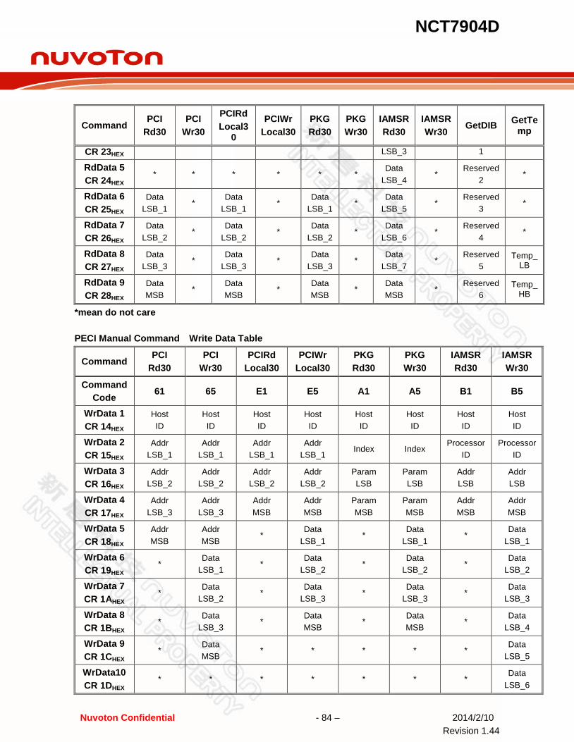
NCT7904D
Nuvoton Confidential - 84 – 2014/2/10 Revision 1.44
Command PCI
Rd30 PCI
Wr30
PCIRd Local3
0
PCIWr Local30
PKG Rd30
PKG Wr30
IAMSR Rd30
IAMSR Wr30
GetDIB GetTemp
CR 23HEX LSB_3 1
RdData 5 CR 24HEX
* * * * * * Data
LSB_4 *
Reserved 2
*
RdData 6 CR 25HEX
Data LSB_1
* Data
LSB_1 *
Data LSB_1
* Data
LSB_5 *
Reserved 3
*
RdData 7 CR 26HEX
Data LSB_2
* Data
LSB_2 *
Data LSB_2
* Data
LSB_6 *
Reserved 4
*
RdData 8 CR 27HEX
Data LSB_3
* Data
LSB_3 *
Data LSB_3
* Data
LSB_7 *
Reserved 5
Temp_LB
RdData 9 CR 28HEX
Data MSB
* Data MSB
* Data MSB
* Data MSB
* Reserved
6 Temp_
HB
*mean do not care PECI Manual Command Write Data Table
Command PCI
Rd30 PCI
Wr30 PCIRd
Local30 PCIWr
Local30 PKG Rd30
PKG Wr30
IAMSR Rd30
IAMSR Wr30
Command Code 61 65 E1 E5 A1 A5 B1 B5
WrData 1 CR 14HEX
Host ID
Host ID
Host ID
Host ID
Host ID
Host ID
Host ID
Host ID
WrData 2 CR 15HEX
Addr LSB_1
Addr LSB_1
Addr LSB_1
Addr LSB_1
Index Index Processor
ID Processor
ID
WrData 3 CR 16HEX
Addr LSB_2
Addr LSB_2
Addr LSB_2
Addr LSB_2
Param LSB
Param LSB
Addr LSB
Addr LSB
WrData 4 CR 17HEX
Addr LSB_3
Addr LSB_3
Addr MSB
Addr MSB
Param MSB
Param MSB
Addr MSB
Addr MSB
WrData 5 CR 18HEX
Addr MSB
Addr MSB
* Data
LSB_1 *
Data LSB_1
* Data
LSB_1
WrData 6 CR 19HEX
* Data
LSB_1 *
Data LSB_2
* Data
LSB_2 *
Data LSB_2
WrData 7 CR 1AHEX
* Data
LSB_2 *
Data LSB_3
* Data
LSB_3 *
Data LSB_3
WrData 8 CR 1BHEX
* Data
LSB_3 *
Data MSB
* Data MSB
* Data
LSB_4
WrData 9 CR 1CHEX
* Data MSB
* * * * * Data
LSB_5
WrData10 CR 1DHEX
* * * * * * * Data
LSB_6
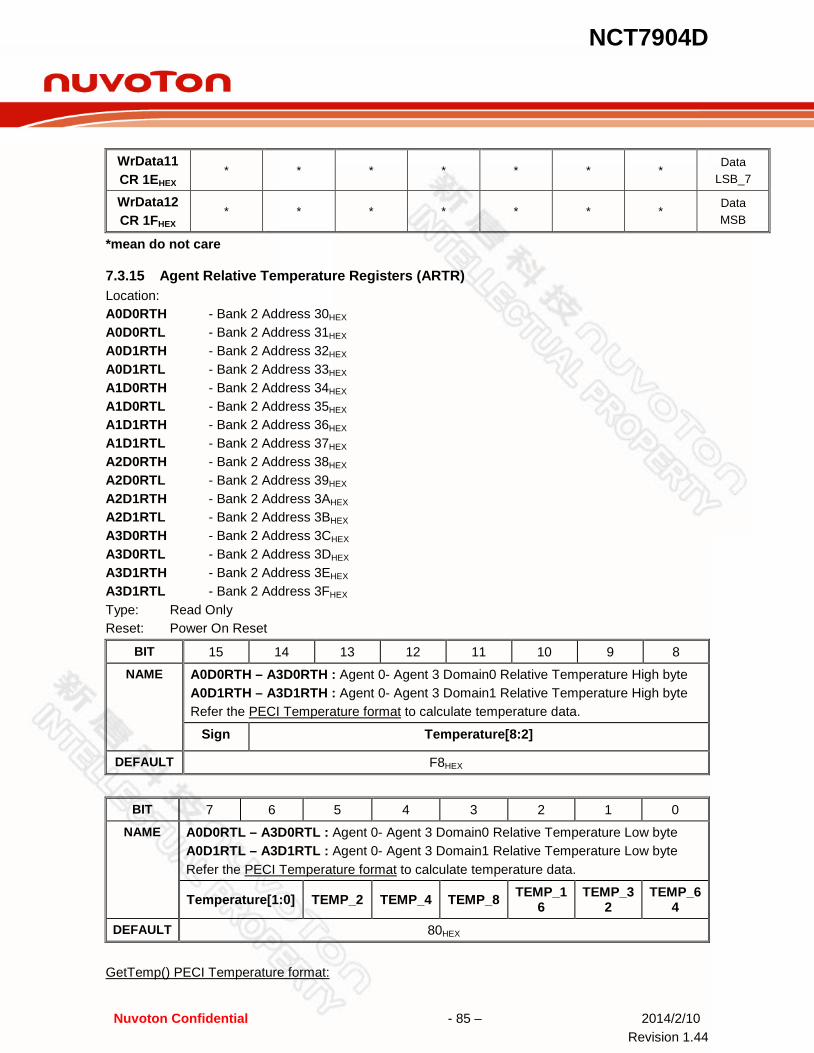
NCT7904D
Nuvoton Confidential - 85 – 2014/2/10 Revision 1.44
WrData11 CR 1EHEX
* * * * * * * Data
LSB_7
WrData12 CR 1FHEX
* * * * * * * Data MSB
*mean do not care
Agent Relative Temperature Registers (ARTR) 7.3.15Location: A0D0RTH - Bank 2 Address 30HEX A0D0RTL - Bank 2 Address 31HEX
A0D1RTH - Bank 2 Address 32HEX A0D1RTL - Bank 2 Address 33HEX A1D0RTH - Bank 2 Address 34HEX A1D0RTL - Bank 2 Address 35HEX
A1D1RTH - Bank 2 Address 36HEX A1D1RTL - Bank 2 Address 37HEX A2D0RTH - Bank 2 Address 38HEX A2D0RTL - Bank 2 Address 39HEX
A2D1RTH - Bank 2 Address 3AHEX A2D1RTL - Bank 2 Address 3BHEX A3D0RTH - Bank 2 Address 3CHEX A3D0RTL - Bank 2 Address 3DHEX A3D1RTH - Bank 2 Address 3EHEX A3D1RTL - Bank 2 Address 3FHEX Type: Read Only Reset: Power On Reset
BIT 15 14 13 12 11 10 9 8 NAME A0D0RTH – A3D0RTH : Agent 0- Agent 3 Domain0 Relative Temperature High byte
A0D1RTH – A3D1RTH : Agent 0- Agent 3 Domain1 Relative Temperature High byte Refer the PECI Temperature format to calculate temperature data.
Sign Temperature[8:2]
DEFAULT F8HEX
BIT 7 6 5 4 3 2 1 0 NAME A0D0RTL – A3D0RTL : Agent 0- Agent 3 Domain0 Relative Temperature Low byte
A0D1RTL – A3D1RTL : Agent 0- Agent 3 Domain1 Relative Temperature Low byte Refer the PECI Temperature format to calculate temperature data.
Temperature[1:0] TEMP_2 TEMP_4 TEMP_8 TEMP_16
TEMP_32
TEMP_64
DEFAULT 80HEX
GetTemp() PECI Temperature format:

NCT7904D
Nuvoton Confidential - 86 – 2014/2/10 Revision 1.44
BIT DESCRIPTION
15 Sign Bit. (Sign) In PECI Protocol, this bit should always be 1 to represent a negative temperature.
14-6 The integer part of the relative temperature. (Temperature[8:0]) 5 TEMP_2. 0.5℃ unit.
4 TEMP_4. 0.25℃ unit.
3 TEMP_8. 0.125℃ unit.
2 TEMP_16. 0.0625℃ unit.
1 TEMP_32. 0.03125℃ unit.
0 TEMP_64. 0.015625℃ unit.
GetTemp() Response Definition:
RESPONSE MEANING
General Sensor Error (GSE)
Thermal scan did not complete in time. Retry is appropriate.
0x0000 Processor is running at its maximum temperature or is currently being reset. All other data Valid temperature reading, reported as a negative offset from the TCC
activation temperature. The valide temperature reading is referred to GetTemp() PECI Temperature format
On some occasions, PECI will return the abnormal states of the PECI bus in addition to the temperature. All the information will be recorded. In some cases, the NCT7904D will also do further processing for the alert mechanism. The following describes these codes and their effects to the NCT7904D.
Error Code Description NCT7904D host operation
8000HEX General Sensor Error No further processing.
8001HEX Sensing Device Missing
8002HEX Operational, but the temperature is
lower than the sensor operation range (underflow).
Compulsorily write -128℃ back to the temperature readouts.
8003HEX Operational, but the temperature is
higher than the sensor operation range. (overflow)
compulsorily write 127℃ back to the temperature readouts.
8004HEX
≀
81FFHEX Reserved. No further operation.
TSI Control Registers 7.3.16Location: Bank 2 Address 50HEX
Type: Read / Write Reset: Power On Reset
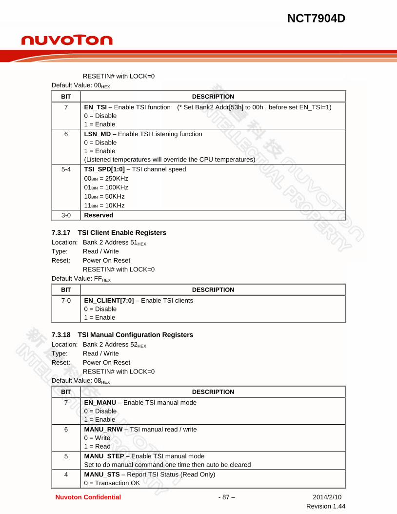
NCT7904D
Nuvoton Confidential - 87 – 2014/2/10 Revision 1.44
RESETIN# with LOCK=0 Default Value: 00HEX
BIT DESCRIPTION
7 EN_TSI – Enable TSI function (* Set Bank2 Addr[53h] to 00h , before set EN_TSI=1) 0 = Disable 1 = Enable
6 LSN_MD – Enable TSI Listening function 0 = Disable 1 = Enable (Listened temperatures will override the CPU temperatures)
5-4 TSI_SPD[1:0] – TSI channel speed 00BIN = 250KHz 01BIN = 100KHz 10BIN = 50KHz 11BIN = 10KHz
3-0 Reserved
TSI Client Enable Registers 7.3.17Location: Bank 2 Address 51HEX
Type: Read / Write Reset: Power On Reset RESETIN# with LOCK=0 Default Value: FFHEX
BIT DESCRIPTION
7-0 EN_CLIENT[7:0] – Enable TSI clients 0 = Disable 1 = Enable
TSI Manual Configuration Registers 7.3.18Location: Bank 2 Address 52HEX
Type: Read / Write Reset: Power On Reset RESETIN# with LOCK=0 Default Value: 08HEX
BIT DESCRIPTION
7 EN_MANU – Enable TSI manual mode 0 = Disable 1 = Enable
6 MANU_RNW – TSI manual read / write 0 = Write 1 = Read
5 MANU_STEP – Enable TSI manual mode Set to do manual command one time then auto be cleared
4 MANU_STS – Report TSI Status (Read Only) 0 = Transaction OK

NCT7904D
Nuvoton Confidential - 88 – 2014/2/10 Revision 1.44
BIT DESCRIPTION 1 = Transaction fail
3 MANU_DONE – TSI Manual Done Status (Read Only) 0 = Transaction done 1 = Transaction still processing
2-0 Reserved
TSI Test Mode Registers 7.3.19Location: Bank 2 Address 53HEX
Type: Read / Write Reset: Power On Reset RESETIN# with LOCK=0 Default Value: 02HEX
BIT DESCRIPTION
7-0 Internal Test Mode Register[7:0] – Set this register to 00h before enable TSI function.
TSI Manual Address Registers 7.3.20Location: Bank 2 Address 54HEX
Type: Read / Write Reset: Power On Reset RESETIN# with LOCK=0 Default Value: 00HEX
BIT DESCRIPTION
7-0 MANU_ADDR[7:0] – TSI manual command address
TSI Manual Command Registers 7.3.21Location: Bank 2 Address 55HEX
Type: Read / Write Reset: Power On Reset RESETIN# with LOCK=0 Default Value: 00HEX
BIT DESCRIPTION
7-0 MANU_CMD[7:0] – TSI manual command data
TSI Manual Write Data Registers 7.3.22Location: Bank 2 Address 56HEX
Type: Read / Write Reset: Power On Reset RESETIN# with LOCK=0 Default Value: 00HEX
BIT DESCRIPTION
7-0 MANU_WDATA[7:0] – TSI manual write data
TSI Manual Read Data Registers 7.3.23

NCT7904D
Nuvoton Confidential - 89 – 2014/2/10 Revision 1.44
Location: Bank 2 Address 57HEX
Type: Read Only Reset: Power On Reset Default Value: 00HEX
BIT DESCRIPTION
7-0 MANU_RDATA[7:0] – TSI manual read data
PCH Read Control Registers 7.3.24Location: Bank 2 Address 60HEX
Type: Read / Write Reset: Power On Reset RESETIN# with LOCK=0 Default Value: 20HEX
BIT DESCRIPTION
7 EN_PCH_RD – Enable PCH read function 0 = Disable 1 = Enable
6 Reserved 5-4 PCH_RD_SPD[1:0] – PCH channel read speed
00BIN = 250KHz 01BIN = 100KHz 10BIN = 50KHz 11BIN = 10KHz
3-0 Reserved
PCH Client Address Registers 7.3.25Location: Bank 2 Address 61HEX
Type: Read / Write Reset: Power On Reset RESETIN# with LOCK=0 Default Value: 00HEX
BIT DESCRIPTION
7-0 PCH_ADDR[7:0] – PCH client address
PCH Command Registers 7.3.26Location: Bank 2 Address 62HEX
Type: Read / Write Reset: Power On Reset RESETIN# with LOCK=0 Default Value: 00HEX
BIT DESCRIPTION
7-0 PCH_CMD[7:0] – PCH command data
PCH Read Byte Count Registers 7.3.27
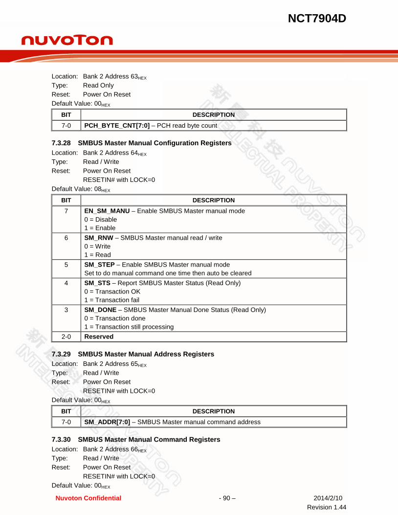
NCT7904D
Nuvoton Confidential - 90 – 2014/2/10 Revision 1.44
Location: Bank 2 Address 63HEX
Type: Read Only Reset: Power On Reset Default Value: 00HEX
BIT DESCRIPTION
7-0 PCH_BYTE_CNT[7:0] – PCH read byte count
SMBUS Master Manual Configuration Registers 7.3.28Location: Bank 2 Address 64HEX
Type: Read / Write Reset: Power On Reset RESETIN# with LOCK=0 Default Value: 08HEX
BIT DESCRIPTION
7 EN_SM_MANU – Enable SMBUS Master manual mode 0 = Disable 1 = Enable
6 SM_RNW – SMBUS Master manual read / write 0 = Write 1 = Read
5 SM_STEP – Enable SMBUS Master manual mode Set to do manual command one time then auto be cleared
4 SM_STS – Report SMBUS Master Status (Read Only) 0 = Transaction OK 1 = Transaction fail
3 SM_DONE – SMBUS Master Manual Done Status (Read Only) 0 = Transaction done 1 = Transaction still processing
2-0 Reserved
SMBUS Master Manual Address Registers 7.3.29Location: Bank 2 Address 65HEX
Type: Read / Write Reset: Power On Reset RESETIN# with LOCK=0 Default Value: 00HEX
BIT DESCRIPTION
7-0 SM_ADDR[7:0] – SMBUS Master manual command address
SMBUS Master Manual Command Registers 7.3.30Location: Bank 2 Address 66HEX
Type: Read / Write Reset: Power On Reset RESETIN# with LOCK=0 Default Value: 00HEX
NCT7904D
Nuvoton Confidential - 91 – 2014/2/10 Revision 1.44
BIT DESCRIPTION
7-0 SM_CMD[7:0] – SMBUS Master manual command data
SMBUS Master Manual Write Data Registers 7.3.31Location: Bank 2 Address 67HEX
Type: Read / Write Reset: Power On Reset RESETIN# with LOCK=0 Default Value: 00HEX
BIT DESCRIPTION
7-0 SM_WDATA[7:0] – SMBUS Master manual write data
SMBUS Master Manual Read Data Registers 7.3.32Location: Bank 2 Address 68HEX
Type: Read Only Reset: Power On Reset Default Value: 00HEX
BIT DESCRIPTION
7-0 SM_RDATA[7:0] – SMBUS Master manual read data
External Read Control Registers 7.3.33Location: Bank 2 Address 6AHEX
Type: Read / Write Reset: Power On Reset RESETIN# with LOCK=0 Default Value: 00HEX
BIT DESCRIPTION
7 EN_EXT_RD – Enable External Read function. 0 = Disable 1 = Enable
6-4 Reserved 3 EN_EXT_P3 – Enable EXT_P3 read function.
0 = Disable 1 = Enable
2 EN_EXT_P2 – Enable EXT_P2 read function. 0 = Disable 1 = Enable
1 EN_EXT_P1 – Enable EXT_P1 read function. 0 = Disable 1 = Enable
0 EN_EXT_P0 – Enable EXT_P0 read function. 0 = Disable 1 = Enable

NCT7904D
Nuvoton Confidential - 92 – 2014/2/10 Revision 1.44
External Read Address and Command Register 7.3.34Location:
EXT_ADDR_P0 - Bank 0 Address 6CHEX EXT_CMD_P0 - Bank 0 Address 6DHEX
EXT_ADDR_P1 - Bank 0 Address 6EHEX EXT_CMD_P1 - Bank 0 Address 6FHEX
EXT_ADDR_P2 - Bank 0 Address 70HEX EXT_CMD_P2 - Bank 0 Address 71HEX
EXT_ADDR_P3 - Bank 0 Address 72HEX EXT_CMD_P3 - Bank 0 Address 73HEX
Type: Read / Write Reset: Power On Reset RESETIN# with LOCK=0 EXT_ADDR_P0 – Port 0 external SMBUS address Location: Bank 2 Address 6CHEX
Default Value: 00HEX
BIT DESCRIPTION
7-0 EXT_ADDR_P0 – Port 0 external SMBUS address
EXT_CMD_P0 – Port 0 external SMBUS command Location: Bank 2 Address 6DHEX
Default Value: 00HEX
BIT DESCRIPTION
7-0 EXT_CMD_P0 – Port 0 external SMBUS command
EXT_ADDR_P1 – Port 1 external SMBUS address Location: Bank 2 Address 6EHEX
Default Value: 00HEX
BIT DESCRIPTION
7-0 EXT_ADDR_P1 – Port 1 external SMBUS address
EXT_CMD_P1 – Port 1 external SMBUS command Location: Bank 2 Address 6FHEX
Default Value: 00HEX
BIT DESCRIPTION
7-0 EXT_CMD_P1 – Port 1 external SMBUS command
EXT_ADDR_P2 – Port 2 external SMBUS address Location: Bank 2 Address 70HEX
Default Value: 00HEX
BIT DESCRIPTION
7-0 EXT_ADDR_P2 – Port 2 external SMBUS address
EXT_CMD_P2 – Port 2 external SMBUS command Location: Bank 2 Address 71HEX
Default Value: 00HEX

NCT7904D
Nuvoton Confidential - 93 – 2014/2/10 Revision 1.44
BIT DESCRIPTION
7-0 EXT_CMD_P2 – Port 2 external SMBUS command
EXT_ADDR_P3 – Port 3 external SMBUS address Location: Bank 2 Address 72HEX
Default Value: 00HEX
BIT DESCRIPTION
7-0 EXT_ADDR_P3 – Port 3 external SMBUS address
EXT_CMD_P3 – Port 3 external SMBUS command Location: Bank 2 Address 73HEX
Default Value: 00HEX
BIT DESCRIPTION
7-0 EXT_CMD_P3 – Port 3 external SMBUS command
Power Unit Status 7.3.35Location: Bank 2 Address 80HEX
Type: Read / Write Reset: Power On Reset RESETIN# with LOCK=0
Power_Unit
BIT 7 6 5 4 3 2 1 0 NAME Reserved Power_Unit[3:0]
DEFAULT 03HEX
BIT DESCRIPTION
7-4 Reserved 3-0 Power_Unit[3:0] – Unit index for power data retrieved from CPU over PECI
The calculation of unit is 1W / 2^Power_Unit. Default is 03h. The manufacture setting will be loaded into as soon as PECI_En assertion. However user could override it by anytime.
Energy Unit Status 7.3.36Location: Bank 2 Address 81HEX
Type: Read / Write Reset: Power On Reset RESETIN# with LOCK=0
Energy_Unit
BIT 7 6 5 4 3 2 1 0 NAME Reserved Energy_Unit[4:0]
DEFAULT 10HEX
BIT DESCRIPTION
NCT7904D
Nuvoton Confidential - 94 – 2014/2/10 Revision 1.44
BIT DESCRIPTION
7-5 Reserved 4-0 Energy_Unit[4:0] – Unit index for energy data retrieved from CPU over PECI
The calculation of unit is 1J / 2^Energy_Unit. Default is 10h. The manufacture setting will be loaded into as soon as PECI_En assertion. However user could override it by anytime.
Retrieving Margin Status Control Registers 7.3.37Location:
CFG - Bank 2 Address 84HEX
Type: Read / Write Reset: Power On Reset RESETIN# with LOCK=0
CFG
BIT 7 6 5 4 3 2 1 0 NAME Reserved MARGIN_BSEL[1:0]
DEFAULT 00HEX
BIT DESCRIPTION
7-2 Reserved
1-0 MARGIN_BSEL[1:0]: Pick-up selection of margin value among returned four bytes data from RdPkgConfig(). The pick-up data will be put into CR98 ~ CR9B Bit[1:0] = 11 => Select last retrieved byte, MSB Bit[1:0] = 10 => Select 3rd retrieved byte Bit[1:0] = 01 => Select second retrieved byte Bit[1:0] = 00 => Select first retrieved byte, LSB
Location: MARGIN_INDEX - Bank 2 Address 85HEX
Type: Read / Write Reset: Power On Reset RESETIN# with LOCK=0 Default: 00HEX
BIT DESCRIPTION
7-0 MARGIN_INDEX: Index data for executing RdPkgConfig()
Location: MARGIN_PARA_L - Bank 2 Address 86HEX
Type: Read / Write Reset: Power On Reset RESETIN# with LOCK=0 Default: 00HEX
BIT DESCRIPTION
NCT7904D
Nuvoton Confidential - 95 – 2014/2/10 Revision 1.44
7-0 MARGIN_PARA_L: Low byte of parameter data for executing RdPkgConfig()
Location: MARGIN_PARA_H - Bank 2 Address 87HEX
Type: Read / Write Reset: Power On Reset RESETIN# with LOCK=0 Default: 00HEX
BIT DESCRIPTION
7-0 MARGIN_PARA_H: High byte of parameter data for executing RdPkgConfig()
Tjmax Temperature Target Read/Write for CPU Agent (Address : 30h ~ 33h) 7.3.38Location: Tjmax_CPU0 - Bank 2 Address 88HEX
Tjmax_CPU1 - Bank 2 Address 89HEX
Tjmax_CPU2 - Bank 2 Address 8AHEX
Tjmax_CPU3 - Bank 2 Address 8BHEX
Type: Read / Write Reset: Power On Reset RESETIN# with LOCK=0
BIT DESCRIPTION
7-0 Tjmax_CPU0[7:0] – Tjmax data for agent address 30h Tjmax_CPU1[7:0] – Tjmax data for agent address 31h Tjmax_CPU2[7:0] – Tjmax data for agent address 32h Tjmax_CPU3[7:0] – Tjmax data for agent address 33h The manufacture setting will be loaded into as soon as PECI_En assertion. However user could override it by anytime.
Default 00HEX
Tcontrol Temperature Target Read/Write for CPU Agent (Address : 30h ~ 33h) 7.3.39Location: Tjmax_CPU0 - Bank 2 Address 8CHEX
Tjmax_CPU1 - Bank 2 Address 8DHEX
Tjmax_CPU2 - Bank 2 Address 8EHEX
Tjmax_CPU3 - Bank 2 Address 8FHEX
Type: Read / Write Reset: Power On Reset RESETIN# with LOCK=0
BIT DESCRIPTION
7-0 Tcontrol_CPU0[7:0] – Tcontrol data for agent address 30h Tcontrol_CPU1[7:0] – Tcontrol data for agent address 31h Tcontrol_CPU2[7:0] – Tcontrol data for agent address 32h Tcontrol_CPU3[7:0] – Tcontrol data for agent address 33h The manufacture setting will be loaded into as soon as PECI_En assertion.

NCT7904D
Nuvoton Confidential - 96 – 2014/2/10 Revision 1.44
BIT DESCRIPTION However user could override it by anytime.
Default 00HEX
Thermal Design Power (TDP) Status for CPU Agent (Address : 30h ~ 33h) 7.3.40Location: TDP_HB_CPU0 - Bank 2 Address 90HEX
TDP_LB_CPU0 - Bank 2 Address 91HEX
TDP_HB_CPU1 - Bank 2 Address 92HEX
TDP_LB_CPU1 - Bank 2 Address 93HEX
TDP_HB_CPU2 - Bank 2 Address 94HEX
TDP_LB_CPU2 - Bank 2 Address 95HEX
TDP_HB_CPU3 - Bank 2 Address 96HEX
TDP_LB_CPU3 - Bank 2 Address 97HEX
Type: Read / Write Reset: Power On Reset RESETIN# with LOCK=0
TDP_HB_CPUx
BIT 7 6 5 4 3 2 1 0 NAME Reserved TDP_HB_CPUx[6:0]
DEFAULT 00HEX
BIT DESCRIPTION
7 Reserved 6-0 High Byte Data of TDP[14:8]
The manufacture setting will be loaded into as soon as PECI_En assertion. However user could override it by anytime.
TDP_LB_CPUx
BIT 7 6 5 4 3 2 1 0 NAME TDP_HB_CPUx
DEFAULT 00HEX
BIT DESCRIPTION
7-0 Low Byte Data of TDP[7:0] The manufacture setting will be loaded into as soon as PECI_En assertion. However user could override it by anytime.
Margin Status for CPU Agent (Address : 30h ~ 33h) 7.3.41Location: Margin_CPU1 - Bank 2 Address 98HEX Margin_CPU2 - Bank 2 Address 99HEX
Margin_CPU3 - Bank 2 Address 9AHEX

NCT7904D
Nuvoton Confidential - 97 – 2014/2/10 Revision 1.44
Margin_CPU4 - Bank 2 Address 9BHEX
Type: Read Reset: Power On Reset RESETIN# with LOCK=0
Margin_CPUx
BIT 7 6 5 4 3 2 1 0 NAME Margin_CPUx
DEFAULT 00HEX
BIT DESCRIPTION
7-0 Margin status for DTS (Sensor) Based Thermal Spec. If Margin is positive, then CPU die temperature is in relative safe operating region. If margin is negative, then CPU is working with higher temperature risk.
Power Reporting Factor for CPU Agent (Address : 30h ~ 33h) 7.3.42Location: Factor_CPU1 - Bank 2 Address 9CHEX Factor_CPU2 - Bank 2 Address 9DHEX
Factor_CPU3 - Bank 2 Address 9EHEX Factor_CPU4 - Bank 2 Address 9FHEX
Type: Read Reset: Power On Reset RESETIN# with LOCK=0
Factor_CPUx
BIT 7 6 5 4 3 2 1 0 NAME Factor_CPUx
DEFAULT FFHEX
BIT DESCRIPTION 7-0 Factor_CPUx : Power reporting factor.
Power reported over PECI is always higher than actual power. The Factor is to sum up each bit weighting. The weighting of each bit is defined as following. [7] = 0.5 [6] = 0.25 [5] = 0.125 [4] = 0.0625 [3] = 0.03125 [2] = 0.015625 [1] = 0.0078125 [0] = 0.00390625

NCT7904D
Nuvoton Confidential - 98 – 2014/2/10 Revision 1.44
DTS DRAM Temperature Monitor Enable Control Register 7.3.43Location:
EN_MT_CTRL0 - Bank 2 Address C0HEX
EN_MT_CTRL1 - Bank 2 Address C1HEX
EN_T_DM_CTRL - Bank 2 Address C2HEX
Type: Read / Write Reset: Power On Reset RESETIN# with LOCK=0 EN_MT_CTRL0 – Digital Channel Highest Temperature Monitoring Control Register Location: Bank 2 Address C0HEX
Default Value: 00HEX
BIT DESCRIPTION
7 EN_MT_C3_C1 – Enable DTS CPU1 Channel3 highest DIMM temperature monitoring. 0 = Disable 1 = Enable
6 EN_MT_C2_C1 – Enable DTS CPU1 Channel2 highest DIMM temperature monitoring. 0 = Disable 1 = Enable
5 EN_MT_C1_C1 – Enable DTS CPU1 Channel1 highest DIMM temperature monitoring. 0 = Disable 1 = Enable
4 EN_MT_C0_C1 – Enable DTS CPU1 Channel0 highest DIMM temperature monitoring. 0 = Disable 1 = Enable
3 EN_MT_C3_C0 – Enable DTS CPU0 Channel3 highest DIMM temperature monitoring. 0 = Disable 1 = Enable
2 EN_MT_C2_C0 – Enable DTS CPU0 Channel2 highest DIMM temperature monitoring. 0 = Disable 1 = Enable
1 EN_MT_C1_C0 – Enable DTS CPU0 Channel1 highest DIMM temperature monitoring. 0 = Disable 1 = Enable
0 EN_MT_C0_C0 – Enable DTS CPU0 Channel0 highest DIMM temperature monitoring. 0 = Disable 1 = Enable
EN_MT_CTRL1 – Digital Channel Highest Temperature Monitoring Control Register Location: Bank 2 Address C1HEX
Default Value: 00HEX
BIT DESCRIPTION
7-3 Reserved 2 EN_MT_SYS – Enable DTS CPU0 and CPU1 highest DIMM temperature monitoring.
0 = Disable

NCT7904D
Nuvoton Confidential - 99 – 2014/2/10 Revision 1.44
BIT DESCRIPTION 1 = Enable
1 EN_MT_C1 – Enable DTS CPU1 highest DIMM temperature monitoring. 0 = Disable 1 = Enable
0 EN_MT_C0 – Enable DTS CPU0 highest DIMM temperature monitoring. 0 = Disable 1 = Enable
EN_T_DM_CTRL – Digital DIMM Temperature Monitoring Control Register Location: Bank 2 Address C2HEX
Default Value: 00HEX
BIT DESCRIPTION
7 EN_T_C3_C1 – Enable DTS CPU1 Channel3 DIMMs temperature monitoring. 0 = Disable 1 = Enable
6 EN_T_C2_C1 – Enable DTS CPU1 Channel2 DIMMs temperature monitoring. 0 = Disable 1 = Enable
5 EN_T_C1_C1 – Enable DTS CPU1 Channel1 DIMMs temperature monitoring. 0 = Disable 1 = Enable
4 EN_T_C0_C1 – Enable DTS CPU1 Channel0 DIMMs temperature monitoring. 0 = Disable 1 = Enable
3 EN_T_C3_C0 – Enable DTS CPU0 Channel3 DIMMs temperature monitoring. 0 = Disable 1 = Enable
2 EN_T_C2_C0 – Enable DTS CPU0 Channel2 DIMMs temperature monitoring. 0 = Disable 1 = Enable
1 EN_T_C1_C0 – Enable DTS CPU0 Channel1 DIMMs temperature monitoring. 0 = Disable 1 = Enable
0 EN_T_C0_C0 – Enable DTS CPU0 Channel0 DIMMs temperature monitoring. 0 = Disable 1 = Enable

NCT7904D
Nuvoton Confidential - 100 – 2014/2/10 Revision 1.44
DRAM Temperature Value Register (Reterived by PECI RdPkgConfig command) 7.3.44Location:
MT_C0_C0 - Bank 2 Address C4HEX
MT_C1_C0 - Bank 2 Address C5HEX
MT_C2_C0 - Bank 2 Address C6HEX
MT_C3_C0 - Bank 2 Address C7HEX
MT_C0_C1 - Bank 2 Address C8HEX
MT_C1_C1 - Bank 2 Address C9HEX
MT_C2_C1 - Bank 2 Address CAHEX
MT_C3_C1 - Bank 2 Address CBHEX
MT_C0 - Bank 2 Address CCHEX
MT_C1 - Bank 2 Address CDHEX
MT_SYS - Bank 2 Address CEHEX
T_D0C0_C0 - Bank 2 Address D0HEX
T_D1C0_C0 - Bank 2 Address D1HEX
T_D2C0_C0 - Bank 2 Address D2HEX
EN_C0_C0 - Bank 2 Address D3HEX
T_D0C1_C0 - Bank 2 Address D4HEX
T_D1C1_C0 - Bank 2 Address D5HEX
T_D2C1_C0 - Bank 2 Address D6HEX
EN_C1_C0 - Bank 2 Address D7HEX
T_D0C2_C0 - Bank 2 Address D8HEX
T_D1C2_C0 - Bank 2 Address D9HEX
T_D2C2_C0 - Bank 2 Address DAHEX
EN_C2_C0 - Bank 2 Address DBHEX
T_D0C3_C0 - Bank 2 Address DCHEX
T_D1C3_C0 - Bank 2 Address DDHEX
T_D2C3_C0 - Bank 2 Address DEHEX
EN_C3_C0 - Bank 2 Address DFHEX
T_D0C0_C1 - Bank 2 Address E0HEX
T_D1C0_C1 - Bank 2 Address E1HEX
T_D2C0_C1 - Bank 2 Address E2HEX
EN_C0_C1 - Bank 2 Address E3HEX
T_D0C1_C1 - Bank 2 Address E4HEX
T_D1C1_C1 - Bank 2 Address E5HEX
T_D2C1_C1 - Bank 2 Address E6HEX
EN_C1_C1 - Bank 2 Address E7HEX
T_D0C2_C1 - Bank 2 Address E8HEX
T_D1C2_C1 - Bank 2 Address E9HEX
T_D2C2_C1 - Bank 2 Address EAHEX
EN_C2_C1 - Bank 2 Address EBHEX
T_D0C3_C1 - Bank 2 Address ECHEX
T_D1C3_C1 - Bank 2 Address EDHEX
T_D2C3_C1 - Bank 2 Address EEHEX
EN_C3_C1 - Bank 2 Address EFHEX
Type: Read / Write

NCT7904D
Nuvoton Confidential - 101 – 2014/2/10 Revision 1.44
Reset: Power On Reset RESETIN# with LOCK=0 MT_C0_C0 – CPU0 Channel0 Highest DIMM Temperature Value Register Location: Bank 2 Address C4HEX
Default Value: 00HEX
BIT DESCRIPTION
7-0 MT_C0_C0 [7:0] CPU0 Channel0 Highest DIMM Temperature
MT_C1_C0 – CPU0 Channel1 Highest DIMM Temperature Value Register Location: Bank 2 Address C5HEX
Default Value: 00HEX
BIT DESCRIPTION
7-0 MT_C1_C0 [7:0] CPU0 Channel1 Highest DIMM Temperature
MT_C2_C0 – CPU0 Channel2 Highest DIMM Temperature Value Register Location: Bank 2 Address C6HEX
Default Value: 00HEX
BIT DESCRIPTION
7-0 MT_C2_C0 [7:0] CPU0 Channel2 Highest DIMM Temperature
MT_C3_C0 – CPU0 Channel3 Highest DIMM Temperature Value Register Location: Bank 2 Address C7HEX
Default Value: 00HEX
BIT DESCRIPTION
7-0 MT_C3_C0 [7:0] CPU0 Channel3 Highest DIMM Temperature
MT_C0_C1 – CPU1 Channel0 Highest DIMM Temperature Value Register Location: Bank 2 Address C8HEX
Default Value: 00HEX
BIT DESCRIPTION
7-0 MT_C0_C1 [7:0] CPU1 Channel0 Highest DIMM Temperature
MT_C1_C1 – CPU1 Channel1 Highest DIMM Temperature Value Register Location: Bank 2 Address C9HEX
Default Value: 00HEX
BIT DESCRIPTION

NCT7904D
Nuvoton Confidential - 102 – 2014/2/10 Revision 1.44
BIT DESCRIPTION
7-0 MT_C1_C1 [7:0] CPU1 Channel1 Highest DIMM Temperature
MT_C2_C1 – CPU1 Channel2 Highest DIMM Temperature Value Register Location: Bank 2 Address CAHEX
Default Value: 00HEX
BIT DESCRIPTION
7-0 MT_C2_C1 [7:0] CPU1 Channel2 Highest DIMM Temperature
MT_C3_C1 – CPU1 Channel3 Highest DIMM Temperature Value Register Location: Bank 2 Address CBHEX
Default Value: 00HEX
BIT DESCRIPTION
7-0 MT_C3_C1 [7:0] CPU1 Channel3 Highest DIMM Temperature
MT_C0 – CPU0 Highest DIMM Temperature Value Register Location: Bank 2 Address CCHEX
Default Value: 00HEX
BIT DESCRIPTION
7-0 MT_C0 [7:0] CPU0 Highest DIMM Temperature
MT_C1 – CPU1 Highest DIMM Temperature Value Register Location: Bank 2 Address CDHEX
Default Value: 00HEX
BIT DESCRIPTION
7-0 MT_C1 [7:0] CPU1 Highest DIMM Temperature
MT_SYS – CPU0 and CPU1 Highest DIMM Temperature Value Register Location: Bank 2 Address CEHEX
Default Value: 00HEX
BIT DESCRIPTION
7-0 MT_SYS [7:0] CPU0 and CPU1 Highest DIMM Temperature
T_DxC0_C0 – CPU0 Channel0 DIMM0~DIMM2 Temperature Value Register Location: Bank 2 Address D0HEX ~ D2HEX
Default Value: 00HEX
NCT7904D
Nuvoton Confidential - 103 – 2014/2/10 Revision 1.44
BIT DESCRIPTION
7-0 T_D0C0_C0 [7:0] ~ T_D2C0_C0 [7:0] T_D0C0_C0 : CPU0 Channel0 DIMM0 Temperature T_D1C0_C0 : CPU0 Channel0 DIMM1 Temperature T_D2C0_C0 : CPU0 Channel0 DIMM2 Temperature
EN_C0_C0 – Enable Read CPU0 Channel0 DIMM Temperature Register Location: Bank 2 Address D3HEX
Default Value: 07HEX
BIT DESCRIPTION
7-3 Reserved
2 EN_T_DIMM2_CH0_C0 – Enable DTS CPU0 Channel0 DIMM2 temperature monitoring. 0 = Disable 1 = Enable
1 EN_T_DIMM1_CH0_C0 – Enable DTS CPU0 Channel0 DIMM1 temperature monitoring. 0 = Disable 1 = Enable
0 EN_T_DIMM0_CH0_C0 – Enable DTS CPU0 Channel0 DIMM0 temperature monitoring. 0 = Disable 1 = Enable
T_DxC1_C0 – CPU0 Channel1 DIMM0~DIMM2 Temperature Value Register Location: Bank 2 Address D4HEX ~ D6HEX
Default Value: 00HEX
BIT DESCRIPTION
7-0
T_D0C1_C0 [7:0] ~ T_D2C1_C0 [7:0] T_D0C1_C0 : CPU0 Channel1 DIMM0 Temperature T_D1C1_C0 : CPU0 Channel1 DIMM1 Temperature T_D2C1_C0 : CPU0 Channel1 DIMM2 Temperature
EN_C1_C0 – Enable Read CPU0 Channel1 DIMM Temperature Register Location: Bank 2 Address D7HEX
Default Value: 07HEX
BIT DESCRIPTION
7-3 Reserved
2 EN_T_DIMM2_CH1_C0 – Enable DTS CPU0 Channel1 DIMM2 temperature monitoring. 0 = Disable 1 = Enable
1 EN_T_DIMM1_CH1_C0 – Enable DTS CPU0 Channel1 DIMM1 temperature monitoring. 0 = Disable 1 = Enable
0 EN_T_DIMM0_CH1_C0 – Enable DTS CPU0 Channel1 DIMM0 temperature monitoring. 0 = Disable

NCT7904D
Nuvoton Confidential - 104 – 2014/2/10 Revision 1.44
BIT DESCRIPTION 1 = Enable
T_DxC2_C0 – CPU0 Channel2 DIMM0~DIMM2 Temperature Value Register Location: Bank 2 Address D8HEX ~ DAHEX
Default Value: 00HEX
BIT DESCRIPTION
7-0 T_D0C2_C0 [7:0] ~ T_D2C2_C0 [7:0] T_D0C2_C0 : CPU0 Channel2 DIMM0 Temperature T_D1C2_C0 : CPU0 Channel2 DIMM1 Temperature T_D2C2_C0 : CPU0 Channel2 DIMM2 Temperature
EN_C2_C0 – Enable Read CPU0 Channel2 DIMM Temperature Register Location: Bank 2 Address DBHEX
Default Value: 07HEX
BIT DESCRIPTION 7-3 Reserved 2 EN_T_DIMM2_CH2_C0 – Enable DTS CPU0 Channel2 DIMM2 temperature monitoring.
0 = Disable 1 = Enable
1 EN_T_DIMM1_CH2_C0 – Enable DTS CPU0 Channel2 DIMM1 temperature monitoring. 0 = Disable 1 = Enable
0 EN_T_DIMM0_CH2_C0 – Enable DTS CPU0 Channel2 DIMM0 temperature monitoring. 0 = Disable 1 = Enable
T_DxC3_C0 – CPU0 Channel3 DIMM0~DIMM2 Temperature Value Register Location: Bank 2 Address DCHEX ~ DEHEX
Default Value: 00HEX
BIT DESCRIPTION 7-0 T_D0C3_C0 [7:0] ~ T_D2C3_C0 [7:0]
T_D0C3_C0 : CPU0 Channel3 DIMM0 Temperature T_D1C3_C0 : CPU0 Channel3 DIMM1 Temperature T_D2C3_C0 : CPU0 Channel3 DIMM2 Temperature
EN_C3_C0 – Enable Read CPU0 Channel3 DIMM Temperature Register Location: Bank 2 Address DFHEX
Default Value: 07HEX
BIT DESCRIPTION
7-3 Reserved
2 EN_T_DIMM2_CH3_C0 – Enable DTS CPU0 Channel3 DIMM2 temperature monitoring. 0 = Disable 1 = Enable
1 EN_T_DIMM1_CH3_C0 – Enable DTS CPU0 Channel3 DIMM1 temperature monitoring.

NCT7904D
Nuvoton Confidential - 105 – 2014/2/10 Revision 1.44
BIT DESCRIPTION 0 = Disable 1 = Enable
0 EN_T_DIMM0_CH3_C0 – Enable DTS CPU0 Channel3 DIMM0 temperature monitoring. 0 = Disable 1 = Enable
T_DxC0_C1 – CPU1 Channel0 DIMM0~DIMM2 Temperature Value Register Location: Bank 2 Address E0HEX ~ E2HEX
Default Value: 00HEX
BIT DESCRIPTION
7-0 T_D0C0_C1 [7:0] ~ T_D2C0_C1 [7:0] T_D0C0_C1 : CPU1 Channel0 DIMM0 Temperature T_D1C0_C1 : CPU1 Channel0 DIMM1 Temperature T_D2C0_C1 : CPU1 Channel0 DIMM2 Temperature
EN_C0_C1 – Enable Read CPU1 Channel0 DIMM Temperature Register Location: Bank 2 Address E3HEX
Default Value: 07HEX
BIT DESCRIPTION 7-3 Reserved 2 EN_T_DIMM2_CH0_C1 – Enable DTS CPU1 Channel0 DIMM2 temperature monitoring.
0 = Disable 1 = Enable
1 EN_T_DIMM1_CH0_C1 – Enable DTS CPU1 Channel0 DIMM1 temperature monitoring. 0 = Disable 1 = Enable
0 EN_T_DIMM0_CH0_C1 – Enable DTS CPU1 Channel0 DIMM0 temperature monitoring. 0 = Disable 1 = Enable
T_DxC1_C1 – CPU1 Channel1 DIMM0~DIMM2 Temperature Value Register Location: Bank 2 Address E4HEX ~ E6HEX
Default Value: 00HEX
BIT DESCRIPTION 7-0 T_D0C1_C1 [7:0] ~ T_D2C1_C1 [7:0]
T_D0C1_C1 : CPU1 Channel1 DIMM0 Temperature T_D1C1_C1 : CPU1 Channel1 DIMM1 Temperature T_D2C1_C1 : CPU1 Channel1 DIMM2 Temperature
EN_C1_C1 – Enable Read CPU1 Channel1 DIMM Temperature Register Location: Bank 2 Address E7HEX
Default Value: 07HEX
BIT DESCRIPTION
7-3 Reserved

NCT7904D
Nuvoton Confidential - 106 – 2014/2/10 Revision 1.44
BIT DESCRIPTION 2 EN_T_DIMM2_CH1_C1 – Enable DTS CPU1 Channel1 DIMM2 temperature monitoring.
0 = Disable 1 = Enable
1 EN_T_DIMM1_CH1_C1 – Enable DTS CPU1 Channel1 DIMM1 temperature monitoring. 0 = Disable 1 = Enable
0 EN_T_DIMM0_CH1_C1 – Enable DTS CPU1 Channel1 DIMM0 temperature monitoring. 0 = Disable 1 = Enable
T_DxC2_C1 – CPU1 Channel2 DIMM0~DIMM2 Temperature Value Register Location: Bank 2 Address E8HEX ~ EAHEX
Default Value: 00HEX
BIT DESCRIPTION 7-0 T_D0C2_C1 [7:0] ~ T_D2C2_C1 [7:0]
T_D0C2_C1 : CPU1 Channel2 DIMM0 Temperature T_D1C2_C1 : CPU1 Channel2 DIMM1 Temperature T_D2C2_C1 : CPU1 Channel2 DIMM2 Temperature
EN_C2_C1 – Enable Read CPU1 Channel2 DIMM Temperature Register Location: Bank 2 Address EBHEX
Default Value: 07HEX
BIT DESCRIPTION 7-3 Reserved 2 EN_T_DIMM2_CH2_C1 – Enable DTS CPU1 Channel2 DIMM2 temperature monitoring.
0 = Disable 1 = Enable
1 EN_T_DIMM1_CH2_C1 – Enable DTS CPU1 Channel2 DIMM1 temperature monitoring. 0 = Disable 1 = Enable
0 EN_T_DIMM0_CH2_C1 – Enable DTS CPU1 Channel2 DIMM0 temperature monitoring. 0 = Disable 1 = Enable
T_DxC3_C1 – CPU1 Channel3 DIMM0~DIMM2 Temperature Value Register Location: Bank 2 Address ECHEX ~ EEHEX
Default Value: 00HEX
BIT DESCRIPTION
7-0 T_D0C3_C1 [7:0] ~ T_D2C3_C1 [7:0] T_D0C3_C1 : CPU1 Channel3 DIMM0 Temperature T_D1C3_C1 : CPU1 Channel3 DIMM1 Temperature T_D2C3_C1 : CPU1 Channel3 DIMM2 Temperature
EN_C3_C1 – Enable Read CPU1 Channel3 DIMM Temperature Register Location: Bank 2 Address EFHEX
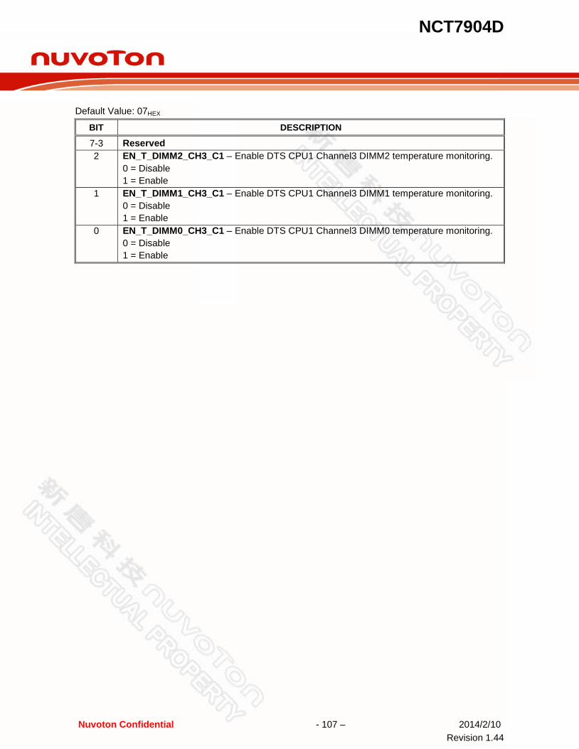
NCT7904D
Nuvoton Confidential - 107 – 2014/2/10 Revision 1.44
Default Value: 07HEX
BIT DESCRIPTION
7-3 Reserved 2 EN_T_DIMM2_CH3_C1 – Enable DTS CPU1 Channel3 DIMM2 temperature monitoring.
0 = Disable 1 = Enable
1 EN_T_DIMM1_CH3_C1 – Enable DTS CPU1 Channel3 DIMM1 temperature monitoring. 0 = Disable 1 = Enable
0 EN_T_DIMM0_CH3_C1 – Enable DTS CPU1 Channel3 DIMM0 temperature monitoring. 0 = Disable 1 = Enable

NCT7904D
Nuvoton Confidential - 108 – 2014/2/10 Revision 1.44
7.4 Bank 3 REGISTER DETAIL
Temperature to Fan Mapping Relationships (TFMR) 7.4.1Location:
T1FMR - Bank 3 Address 00HEX T2FMR - Bank 3 Address 01HEX T3FMR - Bank 3 Address 02HEX
T4FMR - Bank 3 Address 03HEX Type: Read / Write Reset: Power On Reset RESETIN# with LOCK=0
T1FMR – T4FMR
BIT 7 6 5 4 3 2 1 0 NAME Reserved F4SF F3SF F2SF F1SF
DEFAULT 00HEX
BIT DESCRIPTION
7-4 Reserved 3-0 F4SF – F1SF setting involves two purposes. The one is building up the relation between
temperature source 1~4 and FANCTL1~4, the other is Fan Control mode assignment. 0 = Related FANCTL will operate in manual mode and have no relationship with temperature (Default) 1 = Related FANCTL will operate with SmartFan control mode and be linked to relative temperature source 1 ~ 4.
Default Fan Speed at Power-on (DFSP) 7.4.2Location: DFSP - Bank 3 Address 04HEX Type: Read / Write Reset: Power On Reset RESETIN# with LOCK=0
DFSP
BIT 7 6 5 4 3 2 1 0 NAME DefaultSpeed
DEFAULT 7FHEX
BIT DESCRIPTION
7-0 Specify default fan output duty cycle after 3VDD is available

NCT7904D
Nuvoton Confidential - 109 – 2014/2/10 Revision 1.44
SmartFan Output Step Up Time (SFOSUT) 7.4.3Location: SFOSUT - Bank 3 Address 05HEX Type: Read / Write Reset: Power On Reset RESETIN# with LOCK=0
SFOSUT
BIT 7 6 5 4 3 2 1 0 NAME UpTime
DEFAULT 0AHEX
BIT DESCRIPTION
7-0 The update rate for increasing fan output duty cycle. Unit: 0.1sec.
SmartFan Output Step Down Time (SFOSDT) 7.4.4Location: SFOSDT - Bank 3 Address 06HEX
Type: Read / Write Reset: Power On Reset RESETIN# with LOCK=0
SFOSUT
BIT 7 6 5 4 3 2 1 0 NAME DownTime
DEFAULT 0AHEX
BIT DESCRIPTION
7-0 The update rate for decreasing fan output duty cycle. Unit: 0.1sec.
3-Wire Fan Enable and Fan Output Mode Control (FOMC) 7.4.5Location: FOMC - Bank 3 Address 07HEX Type: Read / Write Reset: Power On Reset RESETIN# with LOCK=0
FOMC
BIT 7 6 5 4 3 2 1 0 NAME 3WireFan_En[3:0] F4OMC Reserved
DEFAULT 00HEX
BIT DESCRIPTION
7-4 Enable ultra-low speed DC fan control. It means that DC fan could be driven by very small PWM output frequency or fewer duty cycles.

NCT7904D
Nuvoton Confidential - 110 – 2014/2/10 Revision 1.44
BIT DESCRIPTION 3WireFan_En[3]: Enable FANCTL4 with this function 3WireFan_En[2]: Enable FANCTL3 with this function 3WireFan_En[1]: Enable FANCTL2 with this function 3WireFan_En[0]: Enable FANCTL1 with this function
3 F4OMC: FANCTL4 output mode control. 0 = PWM output (Default) 1 = DC output
2-0 Reserved
Close-Loop Fan control RPM mode and Tolerance (CLFR) 7.4.6Location: CLFR - Bank 3 Address 08HEX Type: Read / Write Reset: Power On Reset RESETIN# with LOCK=0
CLFR
BIT 7 6 5 4 3 2 1 0 NAME RPM_En[3:0] Generic_Tol_RPM
DEFAULT 02HEX
BIT DESCRIPTION
7-4 Close loop (RPM) or Open loop (Fan Duty) Smart Fan control mode selection RPM_En[3] = 1 => Configure FANCTL4 as Close Loop mode, otherwise, it is open loop mode. RPM_En[2] = 1 => Configure FANCTL3 as Close Loop mode, otherwise, it is open loop mode. RPM_En[1] = 1 => Configure FANCTL2 as Close Loop mode, otherwise, it is open loop mode. RPM_En[0] = 1 => Configure FANCTL1 as Close Loop mode, otherwise, it is open loop mode.
3-0 RPM tracking target tolerance. It could suppress the oscillation phenomenon in target RPM lock period. Generic_Tol_RPM: Tolerance of RPM mode, unit is 50 RPMs. If Enable RHSF - Bank 3 Address 0EHEX, unit is 100 RPM.
Temperature Source Selection (TSS) 7.4.7Location:
F1TSS - Bank 3 Address 09HEX F2TSS - Bank 3 Address 0AHEX F3TSS - Bank 3 Address 0BHEX
F4TSS - Bank 3 Address 0CHEX
Type: Read / Write Reset: Power On Reset RESETIN# with LOCK=0
F1TSS – F4TSS
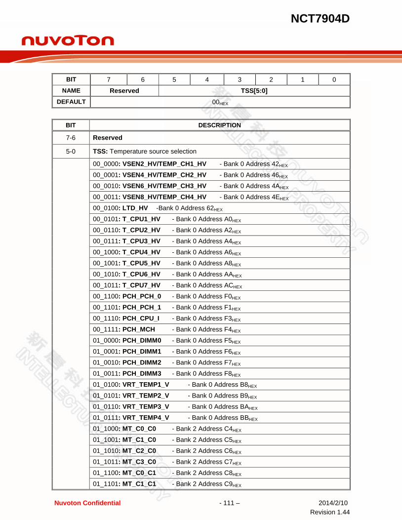
NCT7904D
Nuvoton Confidential - 111 – 2014/2/10 Revision 1.44
BIT 7 6 5 4 3 2 1 0 NAME Reserved TSS[5:0]
DEFAULT 00HEX
BIT DESCRIPTION
7-6 Reserved
5-0 TSS: Temperature source selection
00_0000: VSEN2_HV/TEMP_CH1_HV - Bank 0 Address 42HEX 00_0001: VSEN4_HV/TEMP_CH2_HV - Bank 0 Address 46HEX 00_0010: VSEN6_HV/TEMP_CH3_HV - Bank 0 Address 4AHEX 00_0011: VSEN8_HV/TEMP_CH4_HV - Bank 0 Address 4EHEX 00_0100: LTD_HV -Bank 0 Address 62HEX 00_0101: T_CPU1_HV - Bank 0 Address A0HEX
00_0110: T_CPU2_HV - Bank 0 Address A2HEX
00_0111: T_CPU3_HV - Bank 0 Address A4HEX
00_1000: T_CPU4_HV - Bank 0 Address A6HEX
00_1001: T_CPU5_HV - Bank 0 Address A8HEX
00_1010: T_CPU6_HV - Bank 0 Address AAHEX
00_1011: T_CPU7_HV - Bank 0 Address ACHEX
00_1100: PCH_PCH_0 - Bank 0 Address F0HEX
00_1101: PCH_PCH_1 - Bank 0 Address F1HEX
00_1110: PCH_CPU_I - Bank 0 Address F3HEX
00_1111: PCH_MCH - Bank 0 Address F4HEX
01_0000: PCH_DIMM0 - Bank 0 Address F5HEX
01_0001: PCH_DIMM1 - Bank 0 Address F6HEX
01_0010: PCH_DIMM2 - Bank 0 Address F7HEX
01_0011: PCH_DIMM3 - Bank 0 Address F8HEX
01_0100: VRT_TEMP1_V - Bank 0 Address B8HEX
01_0101: VRT_TEMP2_V - Bank 0 Address B9HEX
01_0110: VRT_TEMP3_V - Bank 0 Address BAHEX
01_0111: VRT_TEMP4_V - Bank 0 Address BBHEX
01_1000: MT_C0_C0 - Bank 2 Address C4HEX
01_1001: MT_C1_C0 - Bank 2 Address C5HEX
01_1010: MT_C2_C0 - Bank 2 Address C6HEX
01_1011: MT_C3_C0 - Bank 2 Address C7HEX
01_1100: MT_C0_C1 - Bank 2 Address C8HEX
01_1101: MT_C1_C1 - Bank 2 Address C9HEX

NCT7904D
Nuvoton Confidential - 112 – 2014/2/10 Revision 1.44
BIT DESCRIPTION
01_1110: MT_C2_C1 - Bank 2 Address CAHEX
01_1111: MT_C3_C1 - Bank 2 Address CBHEX
10_0000: MT_C0 - Bank 2 Address CCHEX
10_0001: MT_C1 - Bank 2 Address CDHEX
10_0010: MT_SYS - Bank 2 Address CEHEX
10_0011: EXT_VRT_TEMP1_V - Bank 0 Address BCHEX
10_0100: EXT_VRT_TEMP2_V - Bank 0 Address BDHEX
10_0101: EXT_VRT_TEMP3_V - Bank 0 Address BEHEX
10_0110: EXT_VRT_TEMP4_V - Bank 0 Address BFHEX
10_0111 ~ 11_1111: Reserved
Power Accumulate Enable (PAE) 7.4.8Location: PAE - Bank 3 Address 0DHEX Type: Read / Write Reset: Power On Reset RESETIN# with LOCK=0
PAE
BIT 7 6 5 4 3 2 1 0 NAME Reserved PWR_MD[3:0]
DEFAULT 00HEX
BIT DESCRIPTION
7-4 Reserved. 3-0 Sensor based fan control mode enabling.
PWR_MD[3] = 1 => FANCTL4 supports sensor based fan control. Otherwise, it is driven by other traditional fan control mode. PWR_MD[2] = 1 => FANCTL3 supports sensor based fan control. Otherwise, it is driven by other traditional fan control mode. PWR_MD[1] = 1 => FANCTL2 supports sensor based fan control. Otherwise, it is driven by other traditional fan control mode. PWR_MD[0] = 1 => FANCTL1 supports sensor based fan control. Otherwise, it is driven by other traditional fan control mode.
Close-Loop Fan Control RPM mode for High Speed Fan Register (RHSF) 7.4.9Location: RHSF - Bank 3 Address 0EHEX Type: Read / Write Reset: Power On Reset RESETIN# with LOCK=0
RHSF
BIT 7 6 5 4 3 2 1 0 NAME SF_TM_U Reserved RPM_HS[3:0]
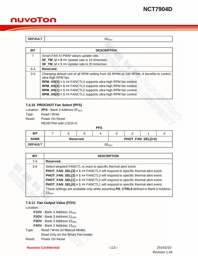
NCT7904D
Nuvoton Confidential - 113 – 2014/2/10 Revision 1.44
DEFAULT 00HEX
BIT DESCRIPTION
7 Smart FAN IV PWM values update rate. SF_TM_U = 0 => Update rate is 10 times/sec. SF_TM_U = 1 => Update rate is 20 times/sec.
6-4 Reserved. 3-0 Changing default unit of all RPM setting from 50 RPMs to 100 RPMs. It benefits to control
ultra-high RPM fan. RPM_HS[3] = 1 => FANCTL4 supports ultra-high RPM fan control. RPM_HS[2] = 1 => FANCTL3 supports ultra-high RPM fan control. RPM_HS[1] = 1 => FANCTL2 supports ultra-high RPM fan control. RPM_HS[0] = 1 => FANCTL1 supports ultra-high RPM fan control.
PROCHOT Fan Select (PFS) 7.4.10Location: PFS - Bank 3 Address 0FHEX Type: Read / Write Reset: Power On Reset RESETIN# with LOCK=0
PFS
BIT 7 6 5 4 3 2 1 0 NAME Reserved PHOT_FAN_SEL[3:0]
DEFAULT 00HEX
BIT DESCRIPTION
7-4 Reserved. 3-0 Select targeted FANCTL to react to specific thermal alert event.
PHOT_FAN_SEL[3] = 1 => FANCTL4 will respond to specific thermal alert event. PHOT_FAN_SEL[2] = 1 => FANCTL3 will respond to specific thermal alert event. PHOT_FAN_SEL[1] = 1 => FANCTL2 will respond to specific thermal alert event. PHOT_FAN_SEL[0] = 1 => FANCTL1 will respond to specific thermal alert event. These settings are available only while asserting PH_CTRL0 defined in Bank 0 Address 23HEX
Fan Output Value (FOV) 7.4.11Location:
F1OV - Bank 3 Address 10HEX F2OV - Bank 3 Address 11HEX F3OV - Bank 3 Address 12HEX F4OV - Bank 3 Address 13HEX
Type: Read / Write (in Manual Mode) Read Only (in the Smart Fan mode) Reset: Power On Reset
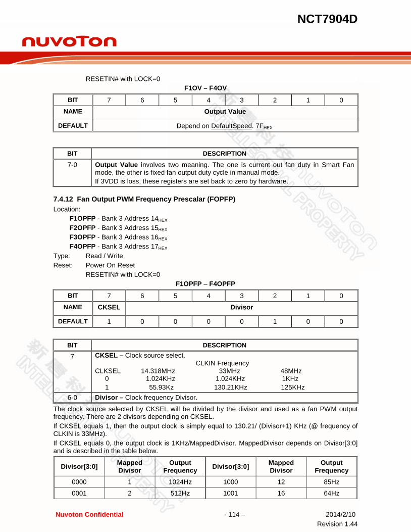
NCT7904D
Nuvoton Confidential - 114 – 2014/2/10 Revision 1.44
RESETIN# with LOCK=0 F1OV – F4OV
BIT 7 6 5 4 3 2 1 0 NAME Output Value
DEFAULT Depend on DefaultSpeed. 7FHEX.
BIT DESCRIPTION
7-0 Output Value involves two meaning. The one is current out fan duty in Smart Fan mode, the other is fixed fan output duty cycle in manual mode. If 3VDD is loss, these registers are set back to zero by hardware.
Fan Output PWM Frequency Prescalar (FOPFP) 7.4.12Location:
F1OPFP - Bank 3 Address 14HEX F2OPFP - Bank 3 Address 15HEX F3OPFP - Bank 3 Address 16HEX F4OPFP - Bank 3 Address 17HEX
Type: Read / Write Reset: Power On Reset RESETIN# with LOCK=0
F1OPFP – F4OPFP
BIT 7 6 5 4 3 2 1 0 NAME CKSEL Divisor
DEFAULT 1 0 0 0 0 1 0 0
BIT DESCRIPTION
7 CKSEL – Clock source select. CLKIN Frequency
CLKSEL 14.318MHz 33MHz 48MHz 0 1.024KHz 1.024KHz 1KHz 1 55.93Kz 130.21KHz 125KHz
6-0 Divisor – Clock frequency Divisor.
The clock source selected by CKSEL will be divided by the divisor and used as a fan PWM output frequency. There are 2 divisors depending on CKSEL. If CKSEL equals 1, then the output clock is simply equal to 130.21/ (Divisor+1) KHz (@ frequency of CLKIN is 33MHz). If CKSEL equals 0, the output clock is 1KHz/MappedDivisor. MappedDivisor depends on Divisor[3:0] and is described in the table below.
Divisor[3:0] Mapped Divisor
Output Frequency Divisor[3:0] Mapped
Divisor Output
Frequency 0000 1 1024Hz 1000 12 85Hz
0001 2 512Hz 1001 16 64Hz

NCT7904D
Nuvoton Confidential - 115 – 2014/2/10 Revision 1.44
Divisor[3:0] Mapped Divisor
Output Frequency Divisor[3:0] Mapped
Divisor Output
Frequency 0010 3 341Hz 1010 32 32Hz
0011 4 256Hz 1011 64 16Hz
0100 5 205Hz 1100 128 8Hz
0101 6 171Hz 1101 256 4Hz
0110 7 146Hz 1110 512 2Hz
0111 8 128Hz 1111 1024 1Hz
Fan Output Nonstop Enable (FONE) 7.4.13Location: FONE - Bank 3 Address 18HEX Type: Read / Write Reset: Power On Reset RESETIN# with LOCK=0
FONE
BIT 7 6 5 4 3 2 1 0
NAME Reserved NON_STOP_En[3:0] DEFAULT 00HEX
BIT DESCRIPTION
7-4 Reserved. 3-0 Enabling the feature that fan could be stopped with special condition. This feature also
requires other setting, including Bank 3 Address 2CHEX , 2DHEX , 2EHEX and 2FHEX in FONV (Fan Output Nonstop Value) NON_STOP_En[3] = 1 => Enable FANCTL4 stop function. NON_STOP_En[2] = 1 => Enable FANCTL3 stop function. NON_STOP_En[1] = 1 => Enable FANCTL2 stop function. NON_STOP_En[0] = 1 => Enable FANCTL1 stop function.
Fan Tachometer Source Selection (FTSS) 7.4.14Location: FTSS - Bank 3 Address 1BHEX
Type: Read / Write Reset: Power On Reset RESETIN# with LOCK=0
FTSS
BIT 7 6 5 4 3 2 1 0 NAME FAN2_SEL FAN1_SEL
DEFAULT 00HEX
BIT DESCRIPTION
7-4 F2FTSS: Fan2 Tachometers Source Selection 3-0 F1FTSS: Fan1 Tachometers Source Selection
NCT7904D
Nuvoton Confidential - 116 – 2014/2/10 Revision 1.44
0000: Source Select FANIN_1 0001: Source Select FANIN_2 0010: Source Select FANIN_3 0011: Source Select FANIN_4 0100: Source Select FANIN_5 0101: Source Select FANIN_6 0110: Source Select FANIN_7 0111: Source Select FANIN_8 1000: Source Select FANIN_9 1001: Source Select FANIN_10 1010: Source Select FANIN_11 1011: Source Select FANIN_12
Fan Tachometer Source Selection (FTSS) 7.4.15Location: FTSS - Bank 3 Address 1CHEX
Type: Read / Write Reset: Power On Reset RESETIN# with LOCK=0
FTSS
BIT 7 6 5 4 3 2 1 0
NAME FAN4_SEL FAN3_SEL DEFAULT 00HEX
BIT DESCRIPTION
7-4 F4FTSS: Fan4 Tachometers Source Selection 3-0 F3FTSS: Fan3 Tachometers Source Selection
0000: Source Select FANIN_1 0001: Source Select FANIN_2 0010: Source Select FANIN_3 0011: Source Select FANIN_4 0100: Source Select FANIN_5 0101: Source Select FANIN_6 0110: Source Select FANIN_7 0111: Source Select FANIN_8 1000: Source Select FANIN_9 1001: Source Select FANIN_10 1010: Source Select FANIN_11 1011: Source Select FANIN_12
Critical Temperature to Full Speed all fan (CTFS) 7.4.16Location:
T1CTFS - Bank 3 Address 20HEX
T2CTFS - Bank 3 Address 21HEX
T3CTFS - Bank 3 Address 22HEX
T4CTFS - Bank 3 Address 23HEX
Type: Read / Write Reset: Power On Reset RESETIN# with LOCK=0
T1CTFS – T4CTFS

NCT7904D
Nuvoton Confidential - 117 – 2014/2/10 Revision 1.44
BIT 7 6 5 4 3 2 1 0 NAME Critical Temperature
DEFAULT 5AHEX (90℃)
BIT DESCRIPTION
7-0 Critical Temperature setting for each Smart Fan Table. While temperature source exceeds the critical temperature, the relative FANCTL will output full duty cycle. Unit in ℃.
Hysteresis of Temperature (HT) 7.4.17Location:
HT1 - Bank 3 Address 24HEX
HT2 - Bank 3 Address 25HEX HT3 - Bank 3 Address 26HEX HT4 - Bank 3 Address 27HEX
Type: Read / Write Reset: Power On Reset RESETIN# with LOCK=0
HT1 – HT4
BIT 7 6 5 4 3 2 1 0 NAME Reserved Hysteresis of Critical
Temperature Reserved Hysteresis of Operation
Temperature
DEFAULT 5HEX (5℃) 3HEX (3℃)
BIT DESCRIPTION
7 Reserved 6-4 Hysteresis of Critical Temperature:
Hysteresis for critical temperature on Smart Fan Table 1 ~ 4. The range is 0℃~7℃
3 Reserved 2-0 Hysteresis of Operation Temperature:
Hysteresis for normal temperature on Smart Fan Table 1 ~ 4. The range is 0℃~7℃
Fan Output Nonstop Value(FONV) 7.4.18Location:
FONV1 - Bank 3 Address 2CHEX
FONV2 - Bank 3 Address 2DHEX
FONV3 - Bank 3 Address 2EHEX
FONV4 - Bank 3 Address 2FHEX
Type: Read / Write Reset: Power On Reset

NCT7904D
Nuvoton Confidential - 118 – 2014/2/10 Revision 1.44
RESETIN# with LOCK=0 FONV1 –FONV4
BIT 7 6 5 4 3 2 1 0 NAME Fan Output Nonstop Value
DEFAULT 14HEX
BIT DESCRIPTION
7-0 Fan Output Nonstop Value for each FANCTL output. If enable FONE - Bank 3 Address 18HEX, the relative FANCTL will output FONV duty cycle.
SMART FANTM IV Temperature and DC/PWM Table (SFIV) 7.4.19Location:
Relative Register-at SMART FANTM IV Control Mode Table
RELATIVE TEMPERAUTRE NNEMONIC ADD (Hex) TYPE
Temp1 T1 – T4 30-33 RW
PWM1 – PWM4 34-37 RW
Temp2 T1 – T4 38-3B RW
PWM1 – PWM4 3C-3F RW
Temp3 T1 – T4 40-43 RW
PWM1 – PWM4 44-47 RW
Temp4 T1 – T4 48-4B RW
DC/PWM1 – DC/PWM4 4C-4F RW
Type: Read / Write Reset: Power On Reset RESETIN# with LOCK=0
T1 – T4
BIT 7 6 5 4 3 2 1 0 NAME SMART FANTM IV Temperature
DEFAULT Table T1 = 19HEX (25℃)
Table T2 = 23HEX (35℃)
Table T3 = 2DHEX (45℃)
Table T4 = 37HEX (55℃)
DC/PWM1 – DC/PWM4
BIT 7 6 5 4 3 2 1 0 NAME SMART FANTM IV DC/PWM
DEFAULT Table P1 = 8CHEX (140 Duty) Table P2 = AAHEX (170 Duty) Table P3 = C8HEX (200 Duty)
NCT7904D
Nuvoton Confidential - 119 – 2014/2/10 Revision 1.44
Table P4 = E6HEX (230 Duty)
Configure Register of PECI Error (CRPE) 7.4.20Location: CRPE - Bank 3 Address 50HEX Type: Read / Write Reset: Power On Reset RESETIN# with LOCK=0
CRPE
BIT 7 6 5 4 3 2 1 0 NAME PECI_ERR_FAN4
BIT[1-0] PECI_ERR_FAN3
BIT[1-0] PECI_ERR_FAN2
BIT[1-0] PECI_ERR_FAN1
BIT[1-0]
Refer to PECI Error Condition Table for fan output value.
DEFAULT 00HEX
BIT DESCRIPTION
7-6 FANCTL4 output state selection while PECI served as temperature source happens any abnormal condition.
5-4 FANCTL3 output state selection while PECI served as temperature source happens any abnormal condition.
3-2 FANCTL2 output state selection while PECI served as temperature source happens any abnormal condition.
1-0 FANCTL1 output state selection while PECI served as temperature source happens any abnormal condition.
PECI Error Condition Table: BIT [1-0] PECI Error Condition 00BIN Fan output value keeps at its current value. 01BIN Fan output value will be set to FOMV (Fan Output Min Value when PECI
Error). 1xBIN Fan output value will be set to the full speed value (FFh).
Fan Output Min Value when PECI Error (FOMV) 7.4.21Location: FOMV - Bank 3 Address 51HEX
Type: Read / Write Reset: Power On Reset RESETIN# with LOCK=0
FOMV
BIT 7 6 5 4 3 2 1 0
NAME FanMin
DEFAULT 80HEX
BIT DESCRIPTION

NCT7904D
Nuvoton Confidential - 120 – 2014/2/10 Revision 1.44
BIT DESCRIPTION
7-0 FanMin: control the FANCTL1-FANCTL4 fan output min value when PECI error condition is occurred. Also see CRPE (Configure Register of PECI Error)
Mask Register of PECI Error (MRPE) 7.4.22Location: MRPE - Bank 3 Address 52HEX Type: Read / Write Reset: Power On Reset RESETIN# with LOCK=0
MRPE
BIT 7 6 5 4 3 2 1 0 NAME Reserved PECI_ERR_MSK[3:0]
DEFAULT 00HEX
BIT DESCRIPTION
7-4 Reserved. 3-0 PECI_ERR_MSK[3:0]: Mask CRPE setting for FANCTL1-FANCTL4. It means that Fan
output value keeps at its current value.
PECI T_DTS Slope Value (PTSV) 7.4.23Location:
P1TSV - Bank 3 Address 64HEX
P2TSV - Bank 3 Address 65HEX
P3TSV - Bank 3 Address 66HEX
P4TSV - Bank 3 Address 67HEX
Type: Read / Write Reset: Power On Reset RESETIN# with LOCK=0
P1TSV – P4TSV
BIT 7 6 5 4 3 2 1 0 NAME PECI T_DTS_Slope
DEFAULT 00HEX
BIT DESCRIPTION

NCT7904D
Nuvoton Confidential - 121 – 2014/2/10 Revision 1.44
BIT DESCRIPTION
7-0 This setting is used to define slope of specific CPU’s DTS Thermal Profile. DTS Thermal profile need to be configured before enabling sensor based fan control algorithm. PECI T_DTS_Slope:
Slope[7]=0.5 Slope[3]=0.03125 Slope[6]=0.25 Slope[2]=0.015625 Slope[5]=0.125 Slope[1]=0.0078125 Slope[4]=0.0625 Slope[0]=0.00390625
Example: PECI T_DTS_Slope[7:0]=8’h46, mean slope=0.273
PECI T_DTS Offset Value (PTOV) 7.4.24Location:
P1TOV - Bank 3 Address 68HEX
P2TOV - Bank 3 Address 69HEX
P3TOV - Bank 3 Address 6AHEX
P4TOV - Bank 3 Address 6BHEX
Type: Read / Write Reset: Power On Reset RESETIN# with LOCK=0
P1TOV – P4TOV
BIT 7 6 5 4 3 2 1 0 NAME PECI T_DTS Offset
DEFAULT 00HEX
BIT DESCRIPTION
7-0 This setting is used to define initial offset temperature of specific CPU’s DTS Thermal Profile. DTS Thermal profile need to be configured before enabling sensor based fan control algorithm.
Tcontrol_Offset Value for CPU Agent (Address : 30h ~ 33h) (TOV) 7.4.25Location:
TOV1 - Bank 3 Address 70HEX
TOV2 - Bank 3 Address 71HEX
TOV3 - Bank 3 Address 72HEX
TOV4 - Bank 3 Address 73HEX
Type: Read / Write Reset: Power On Reset RESETIN# with LOCK=0
TOV1 – TOV4
BIT 7 6 5 4 3 2 1 0 NAME Tcontrol_Offset
NCT7904D
Nuvoton Confidential - 122 – 2014/2/10 Revision 1.44
DEFAULT 00HEX
BIT DESCRIPTION
7-0 Tcontrol_Offset value is required to adjust the Tcontrol_spec desined in DTS(Sensor) Based Thermal Spec. Tcontrol_Offset: Unit in ℃ and 2’s complement representation.
DTS Delta Tolerance Value (DDTV) 7.4.26Location:
DDTV1 - Bank 3 Address 80HEX
DDTV2 - Bank 3 Address 81HEX
DDTV3 - Bank 3 Address 82HEX
DDTV4 - Bank 3 Address 83HEX
Type: Read / Write Reset: Power On Reset RESETIN# with LOCK=0
DDTV1 – DDTV4
BIT 7 6 5 4 3 2 1 0 NAME DTS Delta Tolerance Value
DEFAULT 00HEX
BIT DESCRIPTION
7-0 This setting is used to define Tolerance of DTS (Sensor) Based Fan Control.
DTS Margin Divisor (DMD) 7.4.27Location: DMD - Bank 3 Address 84HEX Type: Read / Write Reset: Power On Reset RESETIN# with LOCK=0
DMD
BIT 7 6 5 4 3 2 1 0 NAME DTS_M_DIV[3:0] Reserved
DEFAULT 00HEX
BIT DESCRIPTION
7-4 Enabling the DTS Margin Divisor. DTS_M_DIV [3] = 1 => Enable FANCTL4 Margin/2. DTS_M_DIV [2] = 1 => Enable FANCTL3 Margin/2. DTS_M_DIV [1] = 1 => Enable FANCTL2 Margin/2. DTS_M_DIV [0] = 1 => Enable FANCTL1 Margin/2.
3-0 Reserved.

NCT7904D
Nuvoton Confidential - 123 – 2014/2/10 Revision 1.44
7.5 Bank 4 REGISTER DETAIL
Temperature to Fan Mapping Relationships (TFMR) 7.5.1Location:
T5FMR - Bank 4 Address 00HEX T6FMR - Bank 4 Address 01HEX T7FMR - Bank 4 Address 02HEX
T8FMR - Bank 4 Address 03HEX
T9FMR - Bank 4 Address 04HEX T10FMR - Bank 4 Address 05HEX
Type: Read / Write Reset: Power On Reset RESETIN# with LOCK=0
T5FMR – T10FMR
BIT 7 6 5 4 3 2 1 0 NAME Reserved F4SF F3SF F2SF F1SF
DEFAULT 00HEX
BIT DESCRIPTION
7-4 Reserved 3-0 F4SF – F1SF setting involves two purposes. The one is building up the relation between
temperature source 5~10 and FANCTL1~4, the other is Fan Control mode assignment. 0 = Related FANCTL will operate in manual mode and have no relationship with temperature (Default) 1 = Related FANCTL will operate with SmartFan control mode and be linked to relative temperature source 5 ~ 10.
Temperature Source Selection (TSS) 7.5.2Location:
TSS5 - Bank 4 Address 08HEX TSS6 - Bank 4 Address 09HEX TSS7 - Bank 4 Address 0AHEX
TSS8 - Bank 4 Address 0BHEX
TSS9 - Bank 4 Address 0CHEX TSS10 - Bank 4 Address 0DHEX
Type: Read / Write Reset: Power On Reset RESETIN# with LOCK=0
F5TSS – F10TSS
BIT 7 6 5 4 3 2 1 0
NAME Reserved TSS[5:0]

NCT7904D
Nuvoton Confidential - 124 – 2014/2/10 Revision 1.44
DEFAULT 00HEX
BIT DESCRIPTION
7-6 Reserved. 5-0 TSS: Temperature source selection
00_0000: VSEN2_HV/TEMP_CH1_HV - Bank 0 Address 42HEX 00_0001: VSEN4_HV/TEMP_CH2_HV - Bank 0 Address 46HEX 00_0010: VSEN6_HV/TEMP_CH3_HV - Bank 0 Address 4AHEX 00_0011: VSEN8_HV/TEMP_CH4_HV - Bank 0 Address 4EHEX 00_0100: LTD_HV -Bank 0 Address 62HEX 00_0101: T_CPU1_HV - Bank 0 Address A0HEX
00_0110: T_CPU2_HV - Bank 0 Address A2HEX
00_0111: T_CPU3_HV - Bank 0 Address A4HEX
00_1000: T_CPU4_HV - Bank 0 Address A6HEX
00_1001: T_CPU5_HV - Bank 0 Address A8HEX
00_1010: T_CPU6_HV - Bank 0 Address AAHEX
00_1011: T_CPU7_HV - Bank 0 Address ACHEX
00_1100: PCH_PCH_0 - Bank 0 Address F0HEX
00_1101: PCH_PCH_1 - Bank 0 Address F1HEX
00_1110: PCH_CPU_I - Bank 0 Address F3HEX
00_1111: PCH_MCH - Bank 0 Address F4HEX
01_0000: PCH_DIMM0 - Bank 0 Address F5HEX
01_0001: PCH_DIMM1 - Bank 0 Address F6HEX
01_0010: PCH_DIMM2 - Bank 0 Address F7HEX
01_0011: PCH_DIMM3 - Bank 0 Address F8HEX
01_0100: VRT_TEMP1_V - Bank 0 Address B8HEX
01_0101: VRT_TEMP2_V - Bank 0 Address B9HEX
01_0110: VRT_TEMP3_V - Bank 0 Address BAHEX
01_0111: VRT_TEMP4_V - Bank 0 Address BBHEX
01_1000: MT_C0_C0 - Bank 2 Address C4HEX
01_1001: MT_C1_C0 - Bank 2 Address C5HEX
01_1010: MT_C2_C0 - Bank 2 Address C6HEX
01_1011: MT_C3_C0 - Bank 2 Address C7HEX
01_1100: MT_C0_C1 - Bank 2 Address C8HEX
01_1101: MT_C1_C1 - Bank 2 Address C9HEX
01_1110: MT_C2_C1 - Bank 2 Address CAHEX
01_1111: MT_C3_C1 - Bank 2 Address CBHEX
10_0000: MT_C0 - Bank 2 Address CCHEX

NCT7904D
Nuvoton Confidential - 125 – 2014/2/10 Revision 1.44
BIT DESCRIPTION
10_0001: MT_C1 - Bank 2 Address CDHEX
10_0010: MT_SYS - Bank 2 Address CEHEX
10_0011: EXT_VRT_TEMP1_V - Bank 0 Address BCHEX
10_0100: EXT_VRT_TEMP2_V - Bank 0 Address BDHEX
10_0101: EXT_VRT_TEMP3_V - Bank 0 Address BEHEX
10_0110: EXT_VRT_TEMP4_V - Bank 0 Address BFHEX
10_0111 ~ 11_1111: Reserved
Critical Temperature to Full Speed all fan (CTFS) 7.5.3Location:
T5CTFS - Bank 4 Address 10HEX
T6CTFS - Bank 4 Address 11HEX
T7CTFS - Bank 4 Address 12HEX
T8CTFS - Bank 4 Address 13HEX
T9CTFS - Bank 4 Address 14HEX
T10CTFS - Bank 4 Address 15HEX
Type: Read / Write Reset: Power On Reset RESETIN# with LOCK=0
T5CTFS – T10CTFS
BIT 7 6 5 4 3 2 1 0 NAME Critical Temperature
DEFAULT 5AHEX (90℃)
BIT DESCRIPTION
7-0 Critical Temperature setting for each Smart Fan Table 5 ~ 10. While temperature source exceeds the critical temperature, the relative FANCTL will output full duty cycle. Unit in ℃.
Hysteresis of Temperature (HT) 7.5.4Location:
HT5 - Bank 4 Address 20HEX
HT6 - Bank 4 Address 21HEX HT7 - Bank 4 Address 22HEX HT8 - Bank 4 Address 23HEX
HT9 - Bank 4 Address 24HEX HT10 - Bank 4 Address 25HEX
Type: Read / Write Reset: Power On Reset RESETIN# with LOCK=0
HT5 – HT10
NCT7904D
Nuvoton Confidential - 126 – 2014/2/10 Revision 1.44
BIT 7 6 5 4 3 2 1 0 NAME Reserved Hysteresis of Critical
Temperature Reserved Hysteresis of Operation
Temperature
DEFAULT 5HEX (5℃) 3HEX (3℃)
BIT DESCRIPTION
7 Reserved 6-4 Hysteresis of Critical Temperature:
Hysteresis for critical temperature on Smart Fan Table 5 ~ 10. The range is 0℃~7℃
3 Reserved 2-0 Hysteresis of Operation Temperature:
Hysteresis for normal temperature on Smart Fan Table 5 ~ 10. The range is 0℃~7℃
SMART FANTM IV Temperature and DC/PWM Table (SFIV) 7.5.5Location:
Relative Register-at SMART FANTM IV Control Mode Table
RELATIVE TEMPERAUTRE NNEMONIC
ADD (Hex)
TYPE
Temp5 T1 – T4 30-33 RW
PWM1 – PWM4 34-37 RW
Temp6 T1 – T4 38-3B RW
PWM1 – PWM4 3C-3F RW
Temp7 T1 – T4 40-43 RW
PWM1 – PWM4 44-47 RW
Temp8 T1 – T4 48-4B RW
DC/PWM1 – DC/PWM4 4C-4F RW
Temp9 T1 – T4 50-53 RW
DC/PWM1 – DC/PWM4 54-57 RW
Temp10 T1 – T4 58-5B RW
DC/PWM1 – DC/PWM4 5C-5F RW
Type: Read / Write Reset: Power On Reset RESETIN# with LOCK=0
T1 – T4
BIT 7 6 5 4 3 2 1 0
NAME SMART FANTM IV Temperature DEFAULT Table T1 = 19HEX (25℃)
Table T2 = 23HEX (35℃)
Table T3 = 2DHEX (45℃)

NCT7904D
Nuvoton Confidential - 127 – 2014/2/10 Revision 1.44
Table T4 = 37HEX (55℃)
DC/PWM1 – DC/PWM4
BIT 7 6 5 4 3 2 1 0
NAME SMART FANTM IV DC/PWM DEFAULT Table P1 = 8CHEX (140 Duty)
Table P2 = AAHEX (170 Duty) Table P3 = C8HEX (200 Duty) Table P4 = E6HEX (230 Duty)

NCT7904D
Nuvoton Confidential - 128 – 2014/2/10 Revision 1.44
8. ELECTRICAL CHARACTERISTICS
8.1 Absolute Maximum Ratings
PARAMETER RATING UNIT
Power Supply Voltage 3VSB,3VDD,VBAT 3.3 ± 5% V
VTT 2.048
Input Voltage -0.3 to +3.6 V
Operating Temperature -20 to +100 *1 ° C
Storage Temperature -55 to +150 ° C
*1 Guaranteed by design from -20~100 degree C, 100% tested at 85 degree C.
8.2 DC Specification (Ta = 0° C to 70° C, 3VDD = 3.3V ± 5%, 3VSB =3.3V ± 5%, GND = 0V)
PARAMETER SYM. MIN. TYP. MAX. UNIT CONDITIONS
OD – Open-drain output pin with source-sink capability of 12 mA
Output Low Voltage VOL 0.4 V IOL = 12 mA
TSI – For AMDTM TSI design
Input Low Voltage VIL 0.6 V
Input High Voltage VIH 1 V
Output Low Voltage VOL 0.285 V
PECI – Bi-direction pin for INTELTM PECI
Input Low Voltage VIL 0.275Vtt 0.5Vtt V
Input High Voltage VIH 0.55Vtt 0.725Vtt V
Output Low Voltage VOL 0.25Vtt V
Output High Voltage VOH 0.75Vtt V
GTL –For PROCHOT,THERMTRIP
Input Low Voltage VIL 0.4 V
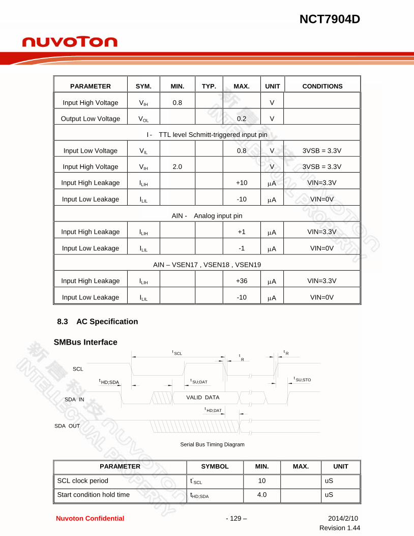
NCT7904D
Nuvoton Confidential - 129 – 2014/2/10 Revision 1.44
PARAMETER SYM. MIN. TYP. MAX. UNIT CONDITIONS
Input High Voltage VIH 0.8 V
Output Low Voltage VOL 0.2 V
I - TTL level Schmitt-triggered input pin
Input Low Voltage VIL 0.8 V 3VSB = 3.3V
Input High Voltage VIH 2.0 V 3VSB = 3.3V
Input High Leakage ILIH +10 µA VIN=3.3V
Input Low Leakage ILIL -10 µA VIN=0V
AIN - Analog input pin
Input High Leakage ILIH +1 µA VIN=3.3V
Input Low Leakage ILIL -1 µA VIN=0V
AIN – VSEN17 , VSEN18 , VSEN19
Input High Leakage ILIH +36 µA VIN=3.3V
Input Low Leakage ILIL -10 µA VIN=0V
8.3 AC Specification SMBus Interface
VALID DATA
SCL
SDA IN
SDA OUT
t HD;SDA
t SCL
t SU;DATt SU;STO
Serial Bus Timing Diagram
t RtR
t HD;DAT
PARAMETER SYMBOL MIN. MAX. UNIT
SCL clock period t-SCL 10 uS
Start condition hold time tHD;SDA 4.0 uS

NCT7904D
Nuvoton Confidential - 130 – 2014/2/10 Revision 1.44
Stop condition setup-up time tSU;STO 4.0 uS
DATA to SCL setup time tSU;DAT 150 nS
DATA to SCL hold time tHD;DAT 270 nS
SCL and SDA rise time tR 1.0 uS
SCL and SDA fall time tF 300 nS
Clock Input Timing
DESCRIPTION CLKIN
MIN TYP MAX
Clock cycle time (1/CLKIN)
x0.97 1/CLKIN
(1/CLKIN) x1.03
Duty cycle 45% 55%

NCT7904D
Nuvoton Confidential - 131 – 2014/2/10 Revision 1.44
9. ORDER INFORMATION PART NO. PACKAGE REMARKS
NCT7904D 48 LQFP (Halogen free)
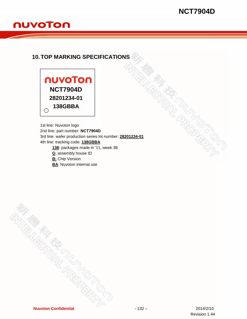
NCT7904D
Nuvoton Confidential - 132 – 2014/2/10 Revision 1.44
10. TOP MARKING SPECIFICATIONS
1st line: Nuvoton logo 2nd line: part number: NCT7904D 3rd line: wafer production series lot number: 28201234-01 4th line: tracking code: 138GBBA
138: packages made in '11, week 38 G: assembly house ID B: Chip Version BA: Nuvoton internal use
NCT7904D 28201234-01
138GBBA
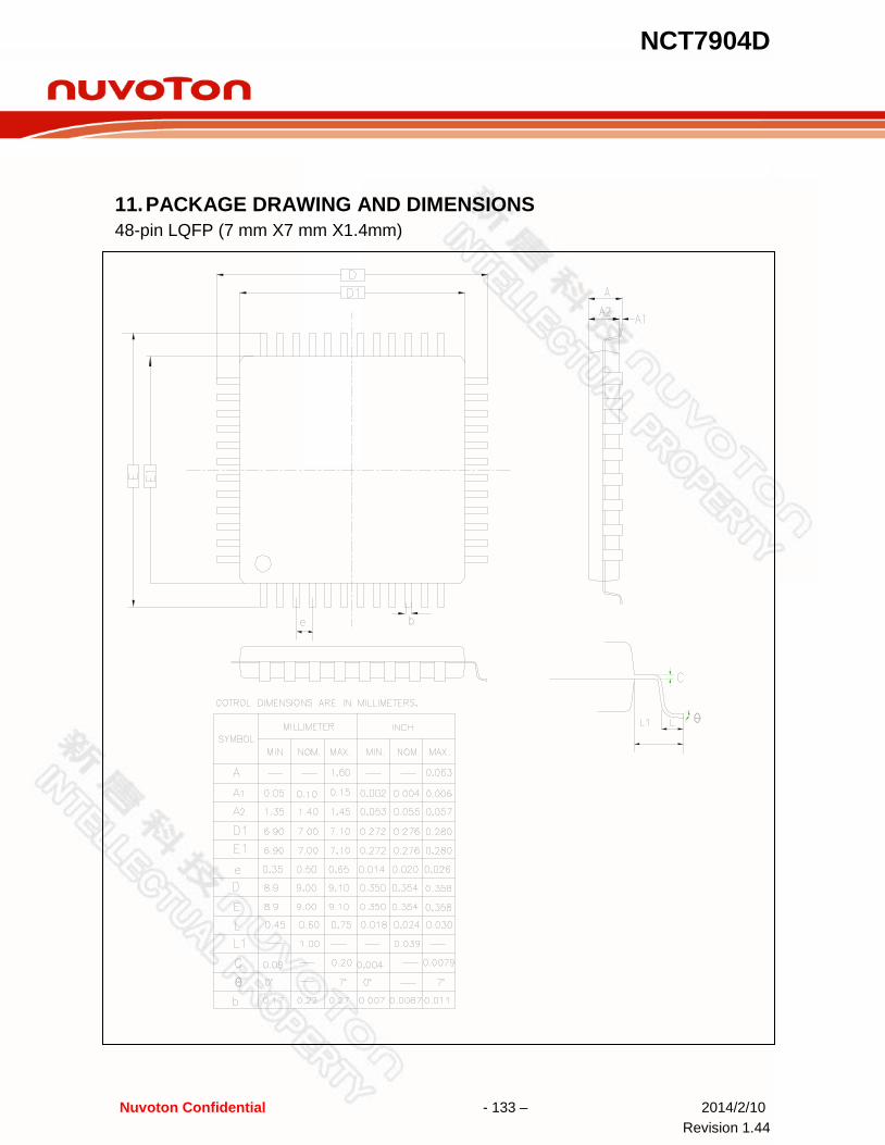
NCT7904D
Nuvoton Confidential - 133 – 2014/2/10 Revision 1.44
11. PACKAGE DRAWING AND DIMENSIONS 48-pin LQFP (7 mm X7 mm X1.4mm)
NCT7904D
Nuvoton Confidential - 134 – 2014/2/10 Revision 1.44
12. REVISION HISTORY VERSION DATE PAGE DESCRIPTION
0.2 08/17/2010 Preliminary Released.
0.3 10/12/2010 ALL Fixed the typos.
0.4 02/25/2011 ALL Updated for new A2 version sample.
0.8 05/04/2011 ALL Updated Top Marketing & Part No.
0.9 08/08/2011 ALL Update for new A3 version sample.
0.91 09/21/2011 The content is the same as v0.9. Just update the version to v0.91 for new A4 version sample.
0.95 11/15/2011 29, 31, 32, 39, 40, 43, 114,
127, 134
1. Update PCH thermal data description (section 6.11.2) 2. Update Device ID information 3. Update LOCK description 4. Update Bank0 Addr[2Eh] Mode Control Register description. 5. Change Temperature Source Selection Table configuration of 00_1100 : from Bank0 Address AEh to F0h 6. Update Order Information (Item 1, 2, 5 are updated for rev.B chip)
1.0 1/5/2012 ALL Public Released. All versions before 1.0 are preliminary versions
1.1 5/31/2012 11,93 1. Fixed the typo. 2. Added External Read Control Register description.
1.2 7/20/2012 114 1.Updated Fan Output PWM Frequency Pre-scalar register.
1.3 2/4/2013 87,88 1. Fixed typo. 2. Updated TSI register descriptions.
1.41 4/11/2013 10,14,15,18,129
1.Modified descriptions for VSEN17,18,19. 2.Fixed typo of VSEN17,18,19 formula. 3.Added DC specification for VSEN17,18,19.
1.42 4/29/2013 27,128 1.Added power ramp request on EEPROM self-initialization function. 2.Modified Absolute Maximum Ratings.
1.43 6/24/2013 13,16 Added recommendations for unused pin.
1.44 2/10/2014 80 Updated description of PECI Power Averaging Configure Register Bit[5].
NCT7904D
Nuvoton Confidential - 135 – 2014/2/10 Revision 1.44
Important Notice Nuvoton Products are neither intended nor warranted for usage in systems or equipment, any malfunction or failure of which may cause loss of human life, bodily injury or severe property damage. Such applications are deemed, “Insecure Usage”.
Insecure usage includes, but is not limited to: equipment for surgical implementation, atomic energy control instruments, airplane or spaceship instruments, the control or operation of dynamic, brake or safety systems designed for vehicular use, traffic signal instruments, all types of safety devices, and other applications intended to support or sustain life.
All Insecure Usage shall be made at customer’s risk, and in the event that third parties lay claims to Nuvoton as a result of customer’s Insecure Usage, customer shall indemnify the damages and liabilities thus incurred by Nuvoton.