NC7SZ57, NC7SZ58 TinyLogic UHS Universal … Sheets/Fairchild PDFs/NC7SZ57,58... · CC operating...
13
NC7SZ57, NC7SZ58 — TinyLogic ® UHS Universal Configurable 2-Input Logic Gates ©2000 Fairchild Semiconductor Corporation www.fairchildsemi.com NC7SZ57, NC7SZ58 Rev. 1.12.0 March 2008 NC7SZ57, NC7SZ58 TinyLogic ® UHS Universal Configurable 2-Input Logic Gates Features ■ Space saving SC70-6 lead surface mount package ■ Ultra small MicroPak™ leadless package ■ Ultra High Speed ■ Capable of implementing any 2-input logic function ■ Typical usage replaces 2 TinyLogic gate devices ■ Reduces part counts in inventory ■ Broad V CC operating range: 1.65V to 5.5V ■ Power down high impedance input/output ■ Overvoltage tolerant inputs facilitate 5V to 3V translation ■ Patented noise/EMI reduction circuitry implemented General Description The NC7SZ57 and the NC7SZ58 are Universal Config- urable 2-Input Logic Gates. Each device is capable of being configured for 1 of 5 unique 2-input logic functions. Any possible 2-input combinatorial logic function can be implemented as shown in the Function Selection Table. Device functionality is selected by how the device is wired at the board level. Figure 1 through Figure 10 illus- trate how to connect the NC7SZ57 and NC7SZ58 respectively for the desired logic function. All inputs have been implemented with hysteresis. The device is fabricated with advanced CMOS technol- ogy to achieve ultra high speed with high output drive while maintaining low static power dissipation over a broad V CC operating range. The device is specified to operate over the 1.65V to 5.5V V CC operating range. The input and output are high impedance when V CC is 0V. Inputs tolerate voltages up to 5.5V independent of V CC operating range. Ordering Information Device also available in Tape and Reel. Specify by appending suffix letter “X” to the ordering number. All packages are lead free per JEDEC: J-STD-020B standard. Order Number Package Number Product Code Top Mark Package Description Supplied As NC7SZ57P6X MAA06A Z57 6-Lead SC70, EIAJ SC88, 1.25mm Wide 3k Units on Tape and Reel NC7SZ57L6X MAC06A KK 6-Lead MicroPak, 1.0mm Wide 5k Units on Tape and Reel NC7SZ58P6X MAA06A Z58 6-Lead SC70, EIAJ SC88, 1.25mm Wide 3k Units on Tape and Reel NC7SZ58L6X MAC06A LL 6-Lead MicroPak, 1.0mm Wide 5k Units on Tape and Reel
-
Upload
vuongkhanh -
Category
Documents
-
view
217 -
download
0
Transcript of NC7SZ57, NC7SZ58 TinyLogic UHS Universal … Sheets/Fairchild PDFs/NC7SZ57,58... · CC operating...

NC
7SZ
57, NC
7SZ
58 — T
inyLo
gic
®
UH
S U
niversal C
on
fig
urab
le 2-Inp
ut L
og
ic Gates
©2NC
March 2008
NC7SZ57, NC7SZ58TinyLogic® UHS Universal Configurable 2-Input Logic Gates
Features Space saving SC70-6 lead surface mount package Ultra small MicroPak™ leadless package Ultra High Speed Capable of implementing any 2-input logic function Typical usage replaces 2 TinyLogic gate devices Reduces part counts in inventory Broad VCC operating range: 1.65V to 5.5V Power down high impedance input/output Overvoltage tolerant inputs facilitate 5V to 3V
translation Patented noise/EMI reduction circuitry implemented
General DescriptionThe NC7SZ57 and the NC7SZ58 are Universal Config-urable 2-Input Logic Gates. Each device is capable ofbeing configured for 1 of 5 unique 2-input logic functions.Any possible 2-input combinatorial logic function can beimplemented as shown in the Function Selection Table.Device functionality is selected by how the device iswired at the board level. Figure 1 through Figure 10 illus-trate how to connect the NC7SZ57 and NC7SZ58respectively for the desired logic function. All inputs havebeen implemented with hysteresis.
The device is fabricated with advanced CMOS technol-ogy to achieve ultra high speed with high output drivewhile maintaining low static power dissipation over abroad VCC operating range. The device is specified tooperate over the 1.65V to 5.5V VCC operating range.The input and output are high impedance when VCC is0V. Inputs tolerate voltages up to 5.5V independent ofVCC operating range.
Ordering Information
Device also available in Tape and Reel. Specify by appending suffix letter “X” to the ordering number.
All packages are lead free per JEDEC: J-STD-020B standard.
OrderNumber
Package Number
Product CodeTop Mark Package Description Supplied As
NC7SZ57P6X MAA06A Z57 6-Lead SC70, EIAJ SC88, 1.25mm Wide
3k Units on Tape and Reel
NC7SZ57L6X MAC06A KK 6-Lead MicroPak, 1.0mm Wide 5k Units on Tape and Reel
NC7SZ58P6X MAA06A Z58 6-Lead SC70, EIAJ SC88, 1.25mm Wide
3k Units on Tape and Reel
NC7SZ58L6X MAC06A LL 6-Lead MicroPak, 1.0mm Wide 5k Units on Tape and Reel
000 Fairchild Semiconductor Corporation www.fairchildsemi.com7SZ57, NC7SZ58 Rev. 1.12.0

©2NC
NC
7SZ
57, NC
7SZ
58 — T
inyLo
gic
®
UH
S U
niversal C
on
fig
urab
le 2-Inp
ut L
og
ic Gates
Connection DiagramsPin Assignments for SC70
(Top View) NC7SZ57 and NC7SZ58
Pin One Orientation Diagram
AAA = Product Code Top Mark -– see ordering code
Note: Orientation of Top Mark determines Pin One location. Read the top product code mark left to right, Pin One is the lower left pin (see diagram).
Pad Assignment for MicroPak
(Top Thru View)
Pin Description
H = HIGH Logic Level
L = LOW Logic Level
Function Table
Pin Name Description
I0, I1, I2 Data Inputs
Y Output
Inputs NC7SZ57 NC7SZ58
I2 I1 I0Y =
(I0) • (I2) (I1) • (I2)Y =
(I0) • (I2) + (I1) • (I2)
L L L H L
L L H L H
L H L H L
L H H L H
H L L L H
H L H L H
H H L H L
H H H H L
000 Fairchild Semiconductor Corporation www.fairchildsemi.com7SZ57, NC7SZ58 Rev. 1.12.0 2

©2NC
NC
7SZ
57, NC
7SZ
58 — T
inyLo
gic
®
UH
S U
niversal C
on
fig
urab
le 2-Inp
ut L
og
ic Gates
Function Selection Table
Logic Configurations NC7SZ57Figure 1 through Figure 5 show the logical functions that can be implemented using the NC7SZ57. The diagrams show the DeMorgan’s equivalent logic duals for a given 2-input function. Next to the logical implementation is the board level physical implementation of how the pins of the function should be connected.
Figure 1. 2-Input AND Gate
Figure 2. 2-Input NAND with Inverted A Input
Figure 3. 2-Input NAND with Inverted B Input
Figure 4. 2-Input NOR Gate
Figure 5. 2-Input XNOR Gate
2-Input Logic FunctionDevice
SelectionConnection
Configuration2-Input AND NC7SZ57 Figure 12-Input AND with inverted input NC7SZ58 Figure 7, Figure 82-Input AND with both inputs inverted NC7SZ57 Figure 42-Input NAND NC7SZ58 Figure 62-Input NAND with inverted input NC7SZ57 Figure 2, Figure 32-Input NAND with both inputs inverted NC7SZ58 Figure 92-Input OR NC7SZ58 Figure 92-Input OR with inverted input NC7SZ57 Figure 2, Figure 32-Input OR with both inputs inverted NC7SZ58 Figure 62-Input NOR NC7SZ57 Figure 42-Input NOR with inverted input NC7SZ58 Figure 7, Figure 82-Input NOR with both inputs inverted NC7SZ57 Figure 12-Input XOR NC7SZ58 Figure 102-Input XNOR NC7SZ57 Figure 5
000 Fairchild Semiconductor Corporation www.fairchildsemi.com7SZ57, NC7SZ58 Rev. 1.12.0 3

©2NC
NC
7SZ
57, NC
7SZ
58 — T
inyLo
gic
®
UH
S U
niversal C
on
fig
urab
le 2-Inp
ut L
og
ic
Logic Configurations NC7SZ58Figure 6 through Figure 10 show the logical functions that can be implemented using the NC7SZ58. The diagrams show the DeMorgan’s equivalent logic duals for a given 2-input function. Next to the logical implementation is the board level physical implementation of how the pins of the function should be connected.
Figure 6. 2-Input NAND Gate
Figure 7. 2-Input AND with Inverted A Input
Figure 8. 2-Input AND with Inverted B Input
Figure 9. 2-Input OR Gate
Figure 10. 2-Input XOR Gate
000 Fairchild Semiconductor Corporation www.fairchildsemi.com7SZ57, NC7SZ58 Rev. 1.12.0 4
Gates

©2NC
NC
7SZ
57, NC
7SZ
58 — T
inyLo
gic
®
UH
S U
niversal C
on
fig
urab
le 2-Inp
ut L
og
ic Gates
Absolute Maximum RatingsStresses exceeding the absolute maximum ratings may damage the device. The device may not function or be operable above the recommended operating conditions and stressing the parts to these levels is not recommended. In addition, extended exposure to stresses above the recommended operating conditions may affect device reliability. The absolute maximum ratings are stress ratings only.
Recommended Operating ConditionsThe Recommended Operating Conditions table defines the conditions for actual device operation. Recommended operating conditions are specified to ensure optimal performance to the datasheet specifications. Fairchild does not recommend exceeding them or designing to absolute maximum ratings.
Symbol Parameter Rating
VCC Supply Voltage –0.5V to +7V
VIN DC Input Voltage –0.5V to +7V
VOUT DC Output Voltage –0.5V to +7V
IIK DC Input Diode Current @ VIN ≤ 0.5V –50mA
IOK DC Output Diode Current @ VIN ≤ –0.5V –50mA
IOUT DC Output Current Source/Sink Current ±50mA
ICC/IGND DC VCC or Ground Current ±50mA
TSTG Storage Temperature Range –65°C to +150°C
TJ Max. Junction Temperature Under Bias 150°C
TL Lead Temperature (Soldering, 10 seconds) 260°C
PD Power Dissipation @ +85°C, SC70-6 180mW
Symbol Parameter Rating
VCC Supply Voltage Operating 1.65V to 5.5V
Supply Voltage Data Retention 1.5V to 5.5V
VIN Input Voltage 0V to 5.5V
VOUT Output Voltage 0V to VCC
TA Operating Temperature –40°C to +85°C
θJA Thermal Resistance, SC70-6 350°C/W
000 Fairchild Semiconductor Corporation www.fairchildsemi.com7SZ57, NC7SZ58 Rev. 1.12.0 5
©2NC
NC
7SZ
57, NC
7SZ
58 — T
inyLo
gic
®
UH
S U
niversal C
on
fig
urab
le 2-Inp
ut L
og
ic Gates
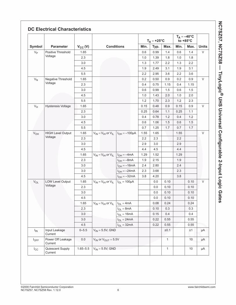
DC Electrical Characteristics
Symbol Parameter VCC (V) Conditions
TA = +25°CTA = –40°C to +85°C
UnitsMin. Typ. Max. Min. Max.
VP Positive Threshold Voltage
1.65 0.6 0.99 1.4 0.6 1.4 V
2.3 1.0 1.39 1.8 1.0 1.8
3.0 1.3 1.77 2.2 1.3 2.2
4.5 1.9 2.49 3.1 1.9 3.1
5.5 2.2 2.95 3.6 2.2 3.6
VN Negative Threshold Voltage
1.65 0.2 0.50 0.9 0.2 0.9 V
2.3 0.4 0.75 1.15 0.4 1.15
3.0 0.6 0.99 1.5 0.6 1.5
4.5 1.0 1.43 2.0 1.0 2.0
5.5 1.2 1.70 2.3 1.2 2.3
VH Hysteresis Voltage 1.65 0.15 0.48 0.9 0.15 0.9 V
2.3 0.25 0.64 1.1 0.25 1.1
3.0 0.4 0.78 1.2 0.4 1.2
4.5 0.6 1.06 1.5 0.6 1.5
5.5 0.7 1.25 1.7 0.7 1.7
VOH HIGH Level Output Voltage
1.65 VIN = VIH or VIL IOH = –100µA 1.55 1.65 1.55 V
2.3 2.2 2.3 2.2
3.0 2.9 3.0 2.9
4.5 4.4 4.5 4.4
1.65 VIN = VIH or VIL IOH = –4mA 1.29 1.52 1.29
2.3 IOH = –8mA 1.9 2.15 1.9
3.0 IOH = –16mA 2.4 2.80 2.4
3.0 IOH = –24mA 2.3 3.68 2.3
4.5 IOH = –32mA 3.8 4.20 3.8
VOL LOW Level Output Voltage
1.65 VIN = VIH or VIL IOL = 100µA 0.0 0.10 0.10 V
2.3 0.0 0.10 0.10
3.0 0.0 0.10 0.10
4.5 0.0 0.10 0.10
1.65 VIN = VIH or VIL IOL = 4mA 0.08 0.24 0.24
2.3 IOL = 8mA 0.10 0.3 0.3
3.0 IOL = 16mA 0.15 0.4 0.4
3.0 IOL = 24mA 0.22 0.55 0.55
4.5 IOL = 32mA 0.22 0.55 0.55
IIN Input Leakage Current
0–5.5 VIN = 5.5V, GND ±0.1 ±1 µA
IOFF Power Off Leakage Current
0.0 VIN or VOUT = 5.5V 1 10 µA
ICC Quiescent Supply Current
1.65–5.5 VIN = 5.5V, GND 1 10 µA
000 Fairchild Semiconductor Corporation www.fairchildsemi.com7SZ57, NC7SZ58 Rev. 1.12.0 6

©2NC
NC
7SZ
57, NC
7SZ
58 — T
inyLo
gic
® UH
S U
niversal C
on
AC Electrical Characteristics
Note:1. CPD is defined as the value of the internal equivalent capacitance which is derived from dynamic operating current
consumption (ICCD) at no output loading and operating at 50% duty cycle. (See Figure 12) CPD is related to ICCD dynamic operatic current by the expression: ICCD = (CPD)(VCC)(fin) + (ICCstatic).
Symbol Parameter VCC (V) Conditions
TA = +25°CTA = –40°C to +85°C
Units Fig. No.Min. Typ. Max. Min. Max.
tPLH, tPHL Propagation Delay In to Y
1.8 ± 0.15 CL = 15pF,RL = 1MΩ
3.0 8 14.0 3.0 14.5 ns Figure 11 Figure 132.5 ± 0.2 1.5 4.9 8.0 1.5 8.5
3.3 ± 0.3 1.2 3.7 5.3 1.2 5.7
5.0 ± 0.5 0.8 2.8 4.3 0.8 4.6
tPLH, tPHL Propagation Delay In to Y
3.3 ± 0.3 CL = 50pF,RL = 500Ω
1.5 4.2 6.0 1.5 6.5 ns Figure 11 Figure 135.0 ± 0.5 1.0 3.4 4.9 1.0 5.3
CIN Input Capacitance 0 2 pF
CPD Power Dissipation 3.3 (1) 14 pF Figure 12
Capacitance 5.0 17
000 Fairchild Semiconductor Corporation www.fairchildsemi.com7SZ57, NC7SZ58 Rev. 1.12.0 7
fig
urab
le 2-Inp
ut L
og
ic Gates

©2NC
NC
7SZ
57, NC
7SZ
58 — T
inyLo
gic
® UH
S U
niversal C
on
fig
urab
le 2-Inp
ut L
og
ic Gates
AC Loading and Waveforms
CL includes load and stray CapacitanceInput PRR = 1.0 MHz, tW = 500 ns
Figure 11. AC Test Circuit
Input = AC WaveformsPRR = Variable; Duty Cycle = 50%
Figure 12. ICCD Test Circuit
Figure 13. AC Waveforms
000 Fairchild Semiconductor Corporation www.fairchildsemi.com7SZ57, NC7SZ58 Rev. 1.12.0 8

©2NC
NC
7SZ
57, NC
7SZ
58 — T
inyLo
gic
® UH
S U
niversal C
on
fig
urab
le 2-Inp
ut L
og
ic Gates
Tape and Reel Specification
Tape Format for SC70
Tape Dimensions inches (millimeters)
Package Designator Tape Section Number of Cavities Cavity Status Cover Tape Status
P6X Leader (Start End) 125 (typ) Empty Sealed
Carrier 3000 Filled Sealed
Trailer (Hub End) 75 (typ) Empty Sealed
Package Tape Size Dim A Dim B Dim F Dim Ko Dim P1 Dim W
SC70-6 8mm 0.093(2.35)
0.096(2.45)
0.138 ± 0.004(3.5 ± 0.10)
0.053 ± 0.004(1.35 ± 0.10)
0.157(4)
0.315 ± 0.004(8 ± 0.1)
000 Fairchild Semiconductor Corporation www.fairchildsemi.com7SZ57, NC7SZ58 Rev. 1.12.0 9

©2NC
NC
7SZ
57, NC
7SZ
58 — T
inyLo
gic
® UH
S U
niversal C
on
fig
urab
le 2-Inp
ut L
og
ic Gates
Tape and Reel Specifications
Tape Format for MicroPak
Reel Dimensions inches (millimeters)
PackageDesignator Tape Section
Number ofCavities Cavity Status
Cover TapeStatus
L6X Leader (Start End) 125 (typ.) Empty Sealed
Carrier 5000 Filled Sealed
Trailer (Hub End) 75 (typ.) Empty Sealed
Tape Size A B C D N W1 W2 W3
8mm 7.0(177.8)
0.059(1.50)
0.512(13.00)
0.795(20.20)
2.165(55.00)
0.331 + 0.059/–0.000(8.40 + 1.50/–0.00)
0.567(14.40)
W1 + 0.078/–0.039(W1 + 2.00/–1.00)
000 Fairchild Semiconductor Corporation www.fairchildsemi.com7SZ57, NC7SZ58 Rev. 1.12.0 10

©2NC
NC
7SZ
57, NC
7SZ
58 — T
inyLo
gic
® UH
S U
niversal C
on
fig
urab
le 2-Inp
ut L
og
ic Gates
Physical Dimensions
Figure 14. 6-Lead SC70, EIAJ SC88, 1.25mm Wide
Package drawings are provided as a service to customers considering Fairchild components. Drawings may change in any mannerwithout notice. Please note the revision and/or date on the drawing and contact a Fairchild Semiconductor representative to verify orobtain the most recent revision. Package specifications do not expand the terms of Fairchild’s worldwide terms and conditions, specifically the warranty therein, which covers Fairchild products.
Always visit Fairchild Semiconductor’s online packaging area for the most recent package drawings: http://www.fairchildsemi.com/packaging/
000 Fairchild Semiconductor Corporation www.fairchildsemi.com7SZ57, NC7SZ58 Rev. 1.12.0 11

©2NC
NC
7SZ
57, NC
7SZ
58 — T
inyLo
gic
® UH
S U
niversal C
on
fig
urab
le 2-Inp
ut L
og
ic Gates
Physical Dimensions (Continued)
Figure 15. 6-Lead MicroPak, 1.0mm Wide
Package drawings are provided as a service to customers considering Fairchild components. Drawings may change in any mannerwithout notice. Please note the revision and/or date on the drawing and contact a Fairchild Semiconductor representative to verify orobtain the most recent revision. Package specifications do not expand the terms of Fairchild’s worldwide terms and conditions, specifically the warranty therein, which covers Fairchild products.
Always visit Fairchild Semiconductor’s online packaging area for the most recent package drawings: http://www.fairchildsemi.com/packaging/
2. DIMENSIONS ARE IN MILLIMETERS1. CONFORMS TO JEDEC STANDARD M0-252 VARIATION UAAD
MAC06AREVC
Notes:
3. DRAWING CONFORMS TO ASME Y14.5M-1994
TOP VIEW
RECOMMENEDLAND PATTERN
BOTTOM VIEW
1.45
1.00
A
B0.05 C
0.05 C
2X
2X
0.55MAX
0.05 C
(0.49)
(1)
(0.75)
(0.52)
(0.30)6X
1X
6X
PIN 1
DETAIL A
0.075 X 45CHAMFER
0.250.15
0.350.25
0.400.30
0.5(0.05)
1.0
5X
DETAIL APIN 1 TERMINAL
0.400.30
0.450.350.10
0.00
0.10 C B A0.05 C
C0.05 C
0.050.00
5X
5X
6X(0.13)4X
6X
000 Fairchild Semiconductor Corporation www.fairchildsemi.com7SZ57, NC7SZ58 Rev. 1.12.0 12
©2NC
NC
7SZ
57, NC
7SZ
58 — T
inyLo
gic
® UH
S U
niversal C
on
fig
urab
le 2-Inp
ut L
og
ic Gates
TRADEMARKSThe following includes registered and unregistered trademarks and service marks, owned by Fairchild Semiconductor and/or its globalsubsidiaries, and is not intended to be an exhaustive list of all such trademarks.
ACEx®
Build it Now™CorePLUS™CROSSVOLT™CTL™Current Transfer Logic™EcoSPARK®
EZSWITCH™ *™
®
Fairchild®
Fairchild Semiconductor®
FACT Quiet Series™FACT®
FAST®
FastvCore™FlashWriter® *
FPS™FRFET®
Global Power ResourceSM
Green FPS™Green FPS™e-Series™GTO™i-Lo™IntelliMAX™ISOPLANAR™MegaBuck™MICROCOUPLER™MicroFET™MicroPak™MillerDrive™Motion-SPM™OPTOLOGIC®
OPTOPLANAR®
®
PDP-SPM™Power220®
POWEREDGE®
Power-SPM™PowerTrench®
Programmable Active Droop™QFET®
QS™QT Optoelectronics™Quiet Series™RapidConfigure™SMART START™SPM®
STEALTH™SuperFET™SuperSOT™-3SuperSOT™-6SuperSOT™-8
SupreMOS™SyncFET™
®
The Power Franchise®
TinyBoost™TinyBuck™TinyLogic®
TINYOPTO™TinyPower™TinyPWM™TinyWire™µSerDes™UHC®
Ultra FRFET™UniFET™VCX™
* EZSWITCH™ and FlashWriter® are trademarks of System General Corporation, used under license by Fairchild Semiconductor.
DISCLAIMERFAIRCHILD SEMICONDUCTOR RESERVES THE RIGHT TO MAKE CHANGES WITHOUT FURTHER NOTICE TO ANY PRODUCTSHEREIN TO IMPROVE RELIABILITY, FUNCTION, OR DESIGN. FAIRCHILD DOES NOT ASSUME ANY LIABILITY ARISING OUT OF THEAPPLICATION OR USE OF ANY PRODUCT OR CIRCUIT DESCRIBED HEREIN; NEITHER DOES IT CONVEY ANY LICENSE UNDER ITSPATENT RIGHTS, NOR THE RIGHTS OF OTHERS. THESE SPECIFICATIONS DO NOT EXPAND THE TERMS OF FAIRCHILD’SWORLDWIDE TERMS AND CONDITIONS, SPECIFICALLY THE WARRANTY THEREIN, WHICH COVERS THESE PRODUCTS.
LIFE SUPPORT POLICYFAIRCHILD’S PRODUCTS ARE NOT AUTHORIZED FOR USE AS CRITICAL COMPONENTS IN LIFE SUPPORT DEVICES ORSYSTEMS WITHOUT THE EXPRESS WRITTEN APPROVAL OF FAIRCHILD SEMICONDUCTOR CORPORATION.
As used herein:1. Life support devices or systems are devices or systems
which, (a) are intended for surgical implant into the body or(b) support or sustain life, and (c) whose failure to performwhen properly used in accordance with instructions for useprovided in the labeling, can be reasonably expected toresult in a significant injury of the user.
2. A critical component in any component of a life support,device, or system whose failure to perform can bereasonably expected to cause the failure of the life supportdevice or system, or to affect its safety or effectiveness.
PRODUCT STATUS DEFINITIONS
Definition of Terms
Datasheet Identification Product Status Definition
Advance Information Formative or In DesignThis datasheet contains the design specifications for productdevelopment. Specifications may change in any manner without notice.
Preliminary First ProductionThis datasheet contains preliminary data; supplementary data will bepublished at a later date. Fairchild Semiconductor reserves the right tomake changes at any time without notice to improve design.
No Identification Needed Full ProductionThis datasheet contains final specifications. Fairchild Semiconductorreserves the right to make changes at any time without notice to improvethe design.
Obsolete Not In ProductionThis datasheet contains specifications on a product that has beendiscontinued by Fairchild Semiconductor. The datasheet is printed forreference information only.
Rev. I33
000 Fairchild Semiconductor Corporation www.fairchildsemi.com7SZ57, NC7SZ58 Rev. 1.12.0 13