Nanostructure Science and...
30
Nanostructure Science and Technology For other titles published in this series go to, http://www.springer.com/series/6331
Transcript of Nanostructure Science and...

Nanostructure Science and Technology
For other titles published in this series go to,http://www.springer.com/series/6331

Patrik Schmuki · Sannakaisa VirtanenEditors
Electrochemistryat the Nanoscale
123

EditorsPatrik Schmuki Sannakaisa VirtanenUniversity of Erlangen-Nuernberg University of Erlangen-NurnbergErlangen, Germany Erlangen, [email protected] [email protected]
ISSN 1571-5744ISBN 978-0-387-73581-8 e-ISBN 978-0-387-73582-5DOI 10.1007/978-0-387-73582-5
Library of Congress Control Number: 2008942146
c© Springer Science+Business Media, LLC 2009All rights reserved. This work may not be translated or copied in whole or in part without the writtenpermission of the publisher (Springer Science+Business Media, LLC, 233 Spring Street, New York,NY 10013, USA), except for brief excerpts in connection with reviews or scholarly analysis. Use inconnection with any form of information storage and retrieval, electronic adaptation, computer software,or by similar or dissimilar methodology now known or hereafter developed is forbidden.The use in this publication of trade names, trademarks, service marks, and similar terms, even if they arenot identified as such, is not to be taken as an expression of opinion as to whether or not they are subjectto proprietary rights.
Printed on acid-free paper
springer.com

Preface
For centuries, electrochemistry has played a key role in technologically importantareas such as electroplating or corrosion. Electrochemical methods are receivingincreasing attention in rapidly growing fields of science and technology, such asnanosciences (nanoelectrochemistry) and life sciences (organic and biological elec-trochemistry). Characterization, modification, and understanding of various electro-chemical interfaces or electrochemical processes at the nanoscale have led to a hugeincrease of scientific interest in electrochemical mechanisms as well as in applica-tion of electrochemical methods to novel technologies. Electrochemical methodscarried out at the nanoscale lead to exciting new science and technology; theseapproaches are described in 12 chapters.
From the fundamental point of view, nanoscale characterization or theoreticalapproaches can lead to an understanding of electrochemical interfaces at the molec-ular level. Not only is this insight of high scientific interest, but also it can be a pre-requisite for controlled technological applications of electrochemistry. Therefore,the book includes fundamental aspects of nanoelectrochemistry.
Then, most important techniques available for electrochemistry on the nanoscaleare presented; this involves both characterization and modification of electrochemi-cal interfaces. Approaches considered include scanning probe techniques,lithography-based approaches, focused-ion and electron beams, and proceduresbased on self-assembly.
In classical fields of electrochemistry, such as corrosion, characterizing surfaceswith a high lateral resolution can lead to an in-depth mechanistic understanding ofthe stability and degradation of materials. The nanoscale description of corrosionprocesses is especially important in understanding the initiation steps of local disso-lution phenomena or in detecting dissolution of highly corrosion-resistant materials.The latter can be of crucial importance in applications, where even the smallestamount of dissolution can lead to a failure of the system (e.g., release of toxicelements and corrosion of microelectronics).
Since many electrochemical processes involve room-temperature treatments inaqueous electrolytes, electrochemical approaches can become extremely importantwhenever living (bio-organic) matter is involved. Hence, a strong demand for elec-trochemical expertise is emerging from biology, where charged interfaces play animportant role. Interfacial electrochemistry is crucially important for understanding
v

vi Preface
the interaction of inorganic substrates with the organic material of biosystems. Thus,recent developments in the field of bioelectrochemistry are described, with a focuson nanoscale phenomena in this field.
Electrochemical methods are of paramount importance for fabrication of nano-materials or nanostructured surfaces. Therefore, several chapters are dedicatedto the electrochemical creation of nanostructured surfaces or nanomaterials. Thisincludes recent developments in the fields of semiconductor porosification, depo-sition into templates, electrodeposition of multilayers and superlattices, as well asself-organized growth of transition metal oxide nanotubes. In all these cases, thenanodimension of the electrochemically prepared materials can lead to novel prop-erties, and hence to novel applications of conventional materials.
We hope that this book will be helpful for all readers interested in electrochem-istry and its applications in various fields of science and technology. Our aim isto present to the reader a comprehensive and contemporary description of electro-chemical nanotechnology.

Contents
Theories and Simulations for Electrochemical Nanostructures . . . . . . . . . . . 1E.P.M. Leiva and Wolfgang Schmickler
SPM Techniques . . . . . . . . . . . . . . . . . . . . . . . . . . . . . . . . . . . . . . . . . . . . . . . . . . . 33O.M. Magnussen
X-ray Lithography Techniques, LIGA-Based MicrosystemManufacturing: The Electrochemistry of Through-Mold Deposition andMaterial Properties . . . . . . . . . . . . . . . . . . . . . . . . . . . . . . . . . . . . . . . . . . . . . . . . . 79James J. Kelly and S.H. Goods
Direct Writing Techniques: Electron Beam and Focused Ion Beam . . . . . . . 139T. Djenizian and C. Lehrer
Wet Chemical Approaches for Chemical Functionalization ofSemiconductor Nanostructures . . . . . . . . . . . . . . . . . . . . . . . . . . . . . . . . . . . . . . 183Rabah Boukherroub and Sabine Szunerits
The Electrochemistry of Porous Semiconductors . . . . . . . . . . . . . . . . . . . . . . . 249John J. Kelly and A.F. van Driel
Deposition into Templates . . . . . . . . . . . . . . . . . . . . . . . . . . . . . . . . . . . . . . . . . . . 279Charles R. Sides and Charles R. Martin
Electroless Fabrication of Nanostructures . . . . . . . . . . . . . . . . . . . . . . . . . . . . . 321T. Osaka
Electrochemical Fabrication of Nanostructured, CompositionallyModulated Metal Multilayers (CMMMs) . . . . . . . . . . . . . . . . . . . . . . . . . . . . . . 349S. Roy
Corrosion at the Nanoscale . . . . . . . . . . . . . . . . . . . . . . . . . . . . . . . . . . . . . . . . . . 377Vincent Maurice and Philippe Marcus
vii

viii Contents
Nanobioelectrochemistry . . . . . . . . . . . . . . . . . . . . . . . . . . . . . . . . . . . . . . . . . . . . 407A.M. Oliveira Brett
Self-Organized Oxide Nanotube Layers on Titanium and OtherTransition Metals . . . . . . . . . . . . . . . . . . . . . . . . . . . . . . . . . . . . . . . . . . . . . . . . . . 435P. Schmuki
Index . . . . . . . . . . . . . . . . . . . . . . . . . . . . . . . . . . . . . . . . . . . . . . . . . . . . . . . . . . . . . 467

Contributors
Rabah Boukherroub Biointerfaces Group, Interdisciplinary Research Institute(IRI), FRE 2963, IRI-IEMN, Avenue Poincare-BP 60069, 59652 Villeneuved’Ascq, France, [email protected]
Thierry Djenizian Laboratoire MADIREL (UMR 6121), Universite deProvence-CNRS, Centre Saint Jerome, F-13397 Marseille Cedex 20, France,[email protected]
A. Floris van Driel Condensed Matter and Interfaces, Debye Institute,Utrecht University, P.O. Box 80000, 3508 TA, Utrecht, The Netherlands,[email protected]
Steven H. Goods Dept. 8758/MS 9402, Sandia National Laboratories, Livermore,CA 94550, USA, [email protected]
James J. Kelly IBM, Electrochemical Processes, 255 Fuller Rd., Albany, NY12203, USA, [email protected]
John J. Kelly Condensed Matter and Interfaces, Debye Institute, Utrecht Univer-sity, P.O. Box 80000, 3508 TA, Utrecht, The Netherlands, [email protected]
Christoph Lehrer Lehrstuhl fur Elektronische Bauelemente, Universitat Erlangen-Nurnberg, Cauerstr. 6, 91058 Erlangen, Germany, [email protected]
Ezequiel P.M. Leiwa Universidad Nacional de Cordoba, Unidad de Matematicay Fisica, Facultad de Ciencias Quimicas, INFIQC, 5000 Cordoba, Argentina,[email protected]
Olaf M. Magnussen Institut fur Experimentelle und AngewandtePhysik, Christian-Albrechts-Universitat zu Kiel, 24098 Kiel, Germany,[email protected]
Philippe Marcus Laboratoire de Physico-Chimie des Surfaces, CNRS-ENSCP(UMR 7045) Ecole Nationale Superieure de Chimie de Paris, UniversitePierre et Marie Curie, 11, rue Pierre et Marie Curie, 75005 Paris, France,[email protected]
ix

x Contributors
Charles R. Martin Department of Chemistry, University of Florida, PO Box117200, Gainesville, FL 32611, USA, [email protected]
Vincent Maurice Laboratoire de Physico-Chimie des Surfaces, CNRS-ENSCP(UMR 7045), Ecole Nationale Superieure de Chimie de Paris, Universite Pierreet Marie Curie, 11, rue Pierre et Marie Curie, 75231 Paris Cedex 05, France,[email protected]
Ana Maria Oliveira Brett Departamento de Quimica, Universidade de Coimbra,3004-535 Coimbra, Portugal, [email protected]
Tetsuya Osaka Department of Applied Chemistry, School of Science andEngineering, Waseda University, 3-4-1 Okubo, Shinjuku-ku, Tokyo, 169-8555,Japan, [email protected]
Sudipta Roy School of Chemical Engineering and Advanced Materials, NewcastleUniversity, Newcastle Upon Tyne NE1 7RU, UK, [email protected]
Wolfgang Schmickler Department of Theoretical Chemistry, University of Ulm,D-89069 Ulm, Germany, [email protected]
Patrik Schmuki University of Erlangen-Nuremberg, Department for MaterialsScience, LKO, Martensstrasse 7, D-91058 Erlangen, Germany, [email protected]
Charles R. Sides Gamry Instruments, Inc., 734 Louis Drive, Warminster, PA18974-2829, USA, [email protected]
Sabine Szunerits INPG, LEMI-ENSEEG, 1130, rue de la piscine, 38402 SaintMartin d’Heres, France, [email protected]
Theories and Simulations for ElectrochemicalNanostructures
E.P.M. Leiva and Wolfgang Schmickler
1 Introduction
Electrochemical nanostructures are special because they can be charged or, equiv-alently, be controlled by the electrode potential. In cases where an auxiliary elec-trode, such as the tip of a scanning tunneling microscope, is employed, there areeven two potential drops that can be controlled individually: the bias potentialbetween the two electrodes and the potential of one electrode with respect to thereference electrode. Thus, electrochemistry offers more possibilities for the genera-tion or modification of nanostructures than systems in air or in vacuum do. However,this advantage carries a price: electrochemical interfaces are more complex, becausethey include the solvent and ions. This poses a great problem for the modeling ofthese interfaces, since it is generally impossible to treat all particles at an equal level.For example, simulations for the generation of metal clusters typically neglect thesolvent, while theories for electron transfer through nanostructures treat the solventin a highly abstract way as a phonon bath. Therefore, a theorist investigating a par-ticular system must decide, in advance, which parts of the system to treat explicitlyand which parts to neglect. Of course, to some extent this is true for all theoreti-cal research, but the more complex the investigated system, the more difficult, anddebatable, this choice becomes.
There is a wide range of nanostructures in electrochemistry, including metal clus-ters, wires, and functionalized layers. Not all of them have been considered by the-orists, and those that have been considered have been treated by various methods.Generally, the generation of nanostructures is too complicated for proper theory,so this has been the domain of computer simulations. In contrast, electron transferthrough nanostructures is amenable to theories based on the Marcus [1] and Hush[2] type of model. There is little overlap between the simulations and the theories,so we cover them in separate sections.
W. Schmickler (B)Department of Theoretical Chemistry, University of Ulm, D-89069 Ulm, Germanye-mail: [email protected]
P. Schmuki, S. Virtanen (eds.), Electrochemistry at the Nanoscale, NanostructureScience and Technology, DOI 10.1007/978-0-387-73582-5 1,C© Springer Science+Business Media, LLC 2009
1
2 E.P.M. Leiva and W. Schmickler
Nanostructures in general are a highly popular area of research, and there is awealth of literature on this topic. Of course, electrochemical nanostructures sharemany properties with nonelectrochemical structures; in this review we will focuson those aspects that are special to electrochemical interfaces, and that thereforedepend on the control of potential or charge density. We shall start by consideringsimulations of electrochemical nanostructures, and shall then turn toward electrontransfer through such structures, in particular through functionalized adsorbates andfilms.
2 Simulations of Electrochemical Nanostructures
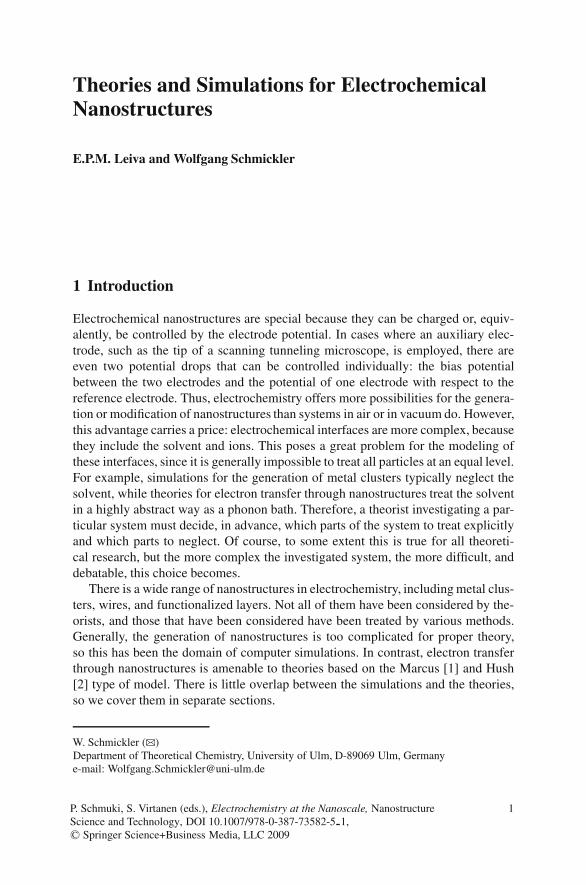
As mentioned in the introduction, electrochemistry offers an ample variety of possi-bilities for the generation of nanostructures, some of which are illustrated in Fig. 1.In this figure, we concentrate on the type of nanostructures that can be obtained bythe application of a scanning probe microscope (SPM), which is the general denom-ination of a device used to image materials at the nanometer scale. In the case ofsurface imaging, the sensitivity of the SPM device to some property of the surface(local electronic density of states, chemical nature, electronic dispersive forces) isused to get some topological information. However, our current interest is relatedto the possibility of using the SPM arrangement to change the atomic ordering andeventually the chemical nature of the surface.
Figure 1a shows the so-called tip-induced local metal deposition, where a scan-ning tunneling microscope (STM) tip is first loaded via electrochemical depositionwith a foreign metal; then the tip is moved to the surface of a substrate, and, uponretraction, a cluster is left behind on the surface. This method works for a num-ber of adsorbate/substrate combinations, but for others it does not, and computer
Fig. 1 Schematic illustrationof several electrochemicaltechniques employed forsurface nanostructuring: (a)Tip-induced local metaldeposition; (b) defectnanostructuring; (c) localizedelectrochemical nucleationand growth; (d) electroniccontact nanostructuring; and(e) scanning electrochemicalmicroscope

Theories and Simulations for Electrochemical Nanostructures 3
simulations have contributed to understanding the formation of the clusters. Figure1b illustrates a different procedure, where a hole is generated by applying a potentialpulse to the STM tip. Then the potential of the substrate is changed to allow con-trolled metal electrodeposition into the cavity. Computer simulations of this type ofprocesses are in a developing stage, with promising results. The method depicted inFig. 1c also starts with metal deposition on the tip, but the metal is then dissolvedby a positive potential pulse that produces local oversaturation of the metal ions,which subsequently nucleate on the surface. Some aspects of this problem havebeen discussed by solving the diffusion equations for the ions generated at the tip.Combinations of techniques (b) and (c) exist, where a foreign metal is depositedon the tip, and a double pulse is applied to it. The first pulse generates a defect onthe surface, and the second pulse desorbs adatoms from the tip that nucleate intothe defect. This method has been simulated using Brownian dynamics. The methoddepicted in Fig. 1d) is employed to generate defects on the surface by means ofsome type of electronic contact between the tip and the surface and has not beenmodeled so far. Finally, the method depicted in Fig. 1e involves the generation ofsome species on the tip that further may react with the surface. This is the basis ofthe technique denominated scanning electrochemical microscopy. While it can beused to image regions of the surface with different electrochemical properties, it canalso be applied to modify, at will, the surface if the latter reacts with the speciesgenerated at the tip. Due to technical limitations, this technique has generally beenapplied in the micrometric rather than in the nanometric scale, but it is a matter ofimprovement to shift its application into the nanometer range.
2.1 Computer Simulation Techniques for Nanostructures
The term computer simulation is so widely used that here a short comment isrequired to clarify the matter. The term simulation is often applied to various numer-ical methods for studying the time dependence of processes. In fact, computers maybe used to solve numerically numerous problems that range from phenomenolog-ical equations to sophisticated quantum mechanical calculations. An electrochem-ical example for the former is the simulation of voltammetric profiles by solvingthe appropriate diffusion equations coupled to an electron-transfer reaction. On theother end of the simulation methods, the time-dependent Schrodinger equation maybe solved to study dynamic processes in an ensemble of particles. Here we referonly to simulations on an atomic scale.
In the simulations of electrochemical nanostructures, we have to deal with a fewhundreds or even thousands of atoms; purely quantum-mechanical calculations ofthe ab initio type are still prohibitive for current computational capabilities. How-ever, since it is expected that at the nanometric scale the atomic nature of atomsmay play a role, it is desirable that the methodology should reflect atomic nature ofmatter, at least in a simplified way. We shall return to this point below.
A typical atomistic computer simulation consists in the generation of a number ofconfigurations of the system of interest, from which the properties in which we are

4 E.P.M. Leiva and W. Schmickler
interested are calculated. From the viewpoint of the way in which the configurationsare generated, the simulations methods are classified into deterministic or stochastic.In the first case, a set of coupled Newton’s equations of the type:
mid2ri
dt2= fi (t) (1)
is solved numerically, where the atomic masses mi and the positions ri are relatedto the forces fi (t) experimented by the particle i at the time t . These forces arecalculated from the potential energy of the system U (rn):
fi = −∇U (rn) (2)
where we denote with rn the set of coordinates of the particles constituting thesystem. Since Eq. (1) contains the time, it is clear that this type of method allowsobtaining dynamic properties of the system. A typical algorithm that performs thenumerical task is, for example, the so-called velocity Verlet algorithm:
ri (t + �t) = ri (t) + vi (t)�t + 1
2
fi (t)
mi�t2 (3)
where vi (t) is the velocity of the particle at time t and �t is an integration step. Therecurrent application of this equation to all the particles of the system leads to atrajectory in the phase space of the system, from which the desired information maybe obtained. We can get a feeling for the �t required for the numerical integrationby inserting into Eq. (3) some typical atomic values. If we want to get a small atomicdisplacement �ri = ri (t + �t) − ri (t), say of the order of 10−3 A for a mass of theorder of 10−23 g, subject to forces of the order of 10−1 eV/A , we get:
�t = O
(√10−23g × 10−11cm
107 eVcm × 1.6 × 10⁻¹² erg
eV
)= O(10−15s) (4)
where 1.6 × 10⁻¹² erg/eV is a conversion factor. The result obtained in Eq. 4 meansthat the integration time required is of the order of a femtosecond, so that a few mil-lion of integration steps will lead us into the nanosecond scale, which are the typicalsimulation times we can reach with current computational resources in nanosystems.
The simulation method discussed so far is the so-called atom or moleculardynamics (MD) procedure and can be employed to calculate both equilibrium andnonequilibrium properties of a system.
In molecular dynamics the generated configurations of the system follow a deter-ministic sequence. However, the trajectory of the system in configuration space maybe chosen differently, following some rules that allow one to obtain sets of coordi-nates of the particles that may later be employed to calculate equilibrium properties.Thus, the main idea underlying stochastic simulation methods is, as in MD, to gen-erate a sequence of configurations. However, the transition probabilities between

Theories and Simulations for Electrochemical Nanostructures 5
them are chosen in such a way that the probability of finding a given configura-tion is given by the equilibrium probability density of the corresponding statisticalthermodynamic ensemble. Making a short summary of equilibrium statistical ther-modynamics, we recall that the first postulate states that an average over a temporalbehavior of given a physical system can be replaced by the average over a collectionof systems or ensemble that exhibits the same thermodynamic but different dynamicproperties. The second postulate refers to isolated systems, where the volume V , theenergy E , and the number of particles N are fixed, and states that the systems in theensemble are uniformly distributed over all the quantum states compatible with theNV E conditions. Besides the NV E or microcanonical ensemble, some other pop-ular ensembles are the canonical ensemble (constant number of particles, volume,and temperature), denoted as NV T , the isothermal isobaric ensemble or N PT ; andthe grand canonical ensemble, where the variables fixed are the chemical potential,volume, and the temperature (μV T ensemble). The molecular dynamics proceduredescribed above is usually run in the (NV E) or NVT ensemble, but other conditionsare also possible.
Returning to the stochastic simulation methods, and taking the NVT ensemble asan example, the transitions between the different configurations are chosen in sucha way that the equilibrium probability density of a certain configuration rn will begiven by:
ρ(rn) = exp (−U (rn)/kT )∫exp (U (r)/kT ) dr
where the integral in the denominator runs over all the possible configurations ofthe system. A way to generate such probability transitions between configurationsis that proposed by Metropolis:
∏mn
= αmnρ(rn)
ρ(rm)= αmn exp [(U (rm) − U (rn)) /kT ] if ρ(rn) < ρ(rn)
∏mn
= αmn if ρ(rn) < ρ(rn)(5)
where �mn is the transition probability from state m to state n, and αmn are constantswhich are restricted to be elements of a symmetric matrix. Thus, a given transitionprobability �mn is obtained by calculating the energy of the system in state m, sayU (rn) and the energy in the state n, say U (rm). The configuration in the n state,given by the vector rn, is obtained from rm by allowing some random motion ofthe system. For example, a particle i may be selected at random, and its coordinatesare displaced from their position r i
n with equal probability to any point r im inside
a small cube surrounding the particle. To accept the move with a probability ofexp [− (U (rn) − U (rm)) /kT ] , a random number ξ is generated with uniform prob-ability density between 0 and 1. If ξ is lower than exp [− (U (rn) − U (rm)) /kT ] itis accepted, otherwise it is rejected. Alternatively, the simultaneous move of all theparticles may be attempted. Similarly to the procedure described above, the energy

6 E.P.M. Leiva and W. Schmickler
values before and after the move attempt to determine the transition probability.The intensive use this technique makes of random (or better stated pseudo-random)numbers has earned it the name of Monte Carlo(MC) method.
In the case of grand canonical or μV T simulations, in addition to the motion ofthe particles, attempts are taken to insert into or remove particles from the system.In this case, all simulation moves must be done in such a way that the probabilitydensity of obtaining a given configuration rn of a system of N particles is given by:
ρ(rn, N) = exp [− (U (rn) + Nμ) /kT ]∑N
∫exp [− (U (r) + Nμ) /kT ] dr
Grand canonical simulations are very useful for simulating electrochemical systems,because a constant electrode potential is equivalent to a constant chemical (or elec-trochemical) potential.
2.2 Interaction Potentials
The main difficulty of computer simulations is that a knowledge of the functionpotential energy functions U (rn) is required to calculate the forces in atom dynam-ics or to calculate the transition probabilities in MC. Strictly speaking, U (rn) stemsfrom the quantum-mechanical interactions between the particles of the system, sothat it should be obtained from first-principles calculations. However, for largeensembles this is not possible, so approximations, or model potentials, are needed.Such potentials are available for many systems: for example, for ionic oxides,closed-shell molecular systems, and fortunately for the problem at hand, for transi-tion metals and their alloys. To the latter class of models belong the so-called gluemodel or the embedded atom method (EAM) [3].
Within the pair-functional scheme, the EAM proposes that the total energy U (rn)of any arrangement of N metal particles may be calculated as the sum of individualparticle energies Ei
U (rn) =N∑
i=1
Ui
where the Ui are
Ui = Fi (ρh,i ) + 1
2
∑j �=i
Vi j(ri j ) (6)
Fi is the embedding function and represents the energy necessary to embed atom iinto the electronic density ρh,i . This latter quantity is calculated at the position ofatom i as the superposition of the individual atomic electronic densities ρi (ri j ) ofthe other particles in the arrangement as:

Theories and Simulations for Electrochemical Nanostructures 7
ρh,i =∑j �=i
ρi (ri j )
The attractive contribution to the energy is given by the embedding function Fi ,which contains the many-body effects in EAM. The repulsive interaction betweenion cores is represented as a pair potential, Vi j (ri j ) which depends exclusively onthe distance between each pair of interacting atoms and has the form of a pseudo-coulombic repulsive energy:
Vi j = Zi (ri j )Z j (ri j )
ri j
where Zi (ri j ) may be considered as an effective charge, which depends upon thenature of particle i . This potential has been adequately parametrized from experi-mental data so as to reproduce a number of parameters as equilibrium lattice con-stants, sublimation energy, bulk modulus, elastic constants and vacancy formationenergy.
2.3 The Creation of Atomic Clusters with the Aid of an STM Tip
As shown in Fig. 1a, an efficient electrochemical method to generate metal clusterson a foreign metal surface consist in moving a metal-loaded tip toward a surface ofdifferent nature. The onset of the interaction between the tip and the surface pro-duces an elongation of the tip at the atomic scale – the so-called jump to contact –that generates a connecting neck between the tip and the surface. After this, the tipmay approach further, and can be retracted at different penetration stages, with var-ious consequences for the generated nanostructure. Experiments with several sys-tems show that this procedure works with several tip/sample combinations, but withothers it fails to produce well-defined surface features. For example, a model systemfor this type of procedure is Cu, deposited on the STM tip, and squashed against aAu(111) surface; for this combination of metals, an array of 10,000 clusters may beproduced in a few minutes [4]. Similarly, with the system Pd/Au(111) well-definednanostructures have been generated [5]. On the other hand, attempts to generateCu clusters on Ag(111) failed; only dispersed monoatomic-high islands have beenobserved [6]. The systems Ag/Au(111) and Pb/Au(111) exhibit of an intermediatebehavior, presenting a wide scatter of cluster sizes and poor reproducibility [6].
Since the creation of the clusters is a dynamic process, the natural computationaltool to study this process appears to be molecular (or more properly stated) atomdynamics. In this respect, it is worth mentioning the pioneering work of Landmanet al. [7], who employed this method to investigate the various atomistic mecha-nisms that occur when a Ni tip interacts with a Au surface. This investigation estab-lished a number of features that were relevant to understand the operating mecha-nism: on the one hand, during the onset of the tip–surface interaction, the occurrenceof a mechanical instability leading to the formation of the connecting neck betweentip and surface mentioned above. On the other hand, and in the subsequent stages

8 E.P.M. Leiva and W. Schmickler
of the nanostructuring process, the existence of a sequence of elastic and plasticdeformation phases that determine the final status of the system. Typically, due tothe time-step limitations mentioned above, the simulations are restricted to a fewnanoseconds. However, the electrochemical generation of nanostructures involvestimes of the order of milliseconds, so that some long-time features of the experi-mental problem will be missing in the simulations. This must be taken into accountfor a careful interpretation of the experimental results in terms of simulations, inthe sense that some slow processes, not observed in the simulations, may occurin experiments. However, the information obtained in the computational studies isimportant in the sense that if some processes are observed, they will certainly occurin the experiments.
A typical atomic arrangement employed for a MD simulation of the generationof clusters is shown in Fig. 2. The simulated tip consists of a rigid core, in thepresent case of Pt atoms, from which mobile atoms of type M to be deposited aresuspended. These amount typically to a couple of thousand atoms, the exact fig-ures for the different systems can be found in reference [8]. Different structureswere assumed for the underlying rigid core. In some simulations a fcc crystallinestructure was assumed, oriented with the (111), or alternatively the (100), latticeplanes facing the substrate. We shall call them [111] and [100] tips, respectively.
Fig. 2 x − y section of atypical atomic arrangementemployed in the simulation oftip-induced local metaldeposition. Dark circlesrepresent atoms belonging tothe STM tip. Transparentcircles denote the atoms of thematerial M being deposited,and light gray circles indicatethe substrate atoms. Thepresence of a monolayeradsorbed on the electrode isdepicted in this case. dts
indicates the distance betweenthe surface and the upper partof the tip. d0 is the initialdistance between the surfaceand the lower part of the tip.Mobile and fixed substratelayers are also marked in thefigure. Taken fromreference [8].

Theories and Simulations for Electrochemical Nanostructures 9
In other simulations, an amorphous structure was assumed [9]. The substrate S wasrepresented by six mobile atom layers on top of two static layers with the fcc(111)orientation. An adsorbed monolayer of the same material as that deposited on thetip was occasionally introduced, so simulate nanostructuring under underpotentialdeposition conditions. Periodic boundary conditions were applied in the x − y plane,parallel to the substrate surface. The tip was moved in z direction in 0.006 A steps,performing first a forward motion toward the surface followed by a stage of back-ward motion. The distances given below will be referred to the jump-to-contact pointdescribed above, and the turning point of the motion of the tip, which determines themagnitude of the indentation, will be denoted with dca. The metallic systems so farinvestigated were Cu/Au(111), Pd/Au(111), Cu/Ag(111), Pb/Au(111), Ag/Au(111),and Cu/Cu(111).
Figure 3 depicts several snapshots of a typical simulation run where clustercreation is successful, in this case for the system Pd[110]/Au(111). The simula-tion starts at a point where the tip–surface interaction is negligible (Fig. 3a). The
Fig. 3 Snapshots of an atom dynamics simulation taken during the generation of a Pd clusteron Au(111): (a) initial state; (b) jump-to-contact from the tip to the surface; (c) closest approachdistance; (d) connecting neck elongation; and (e) final configuration. The resulting cluster has 256atoms, is eight layers high and its composition is 16% in Au. Taken from reference [10]

10 E.P.M. Leiva and W. Schmickler
approach of the tip to the surface leads to the jump-to-contact process, wheremechanical contact between the tip and the surface sets in (Fig. 3b). A furtherapproach of the tip results in an indentation stage (Fig. 3c), where the interactionbetween the tip and the surface is strong enough to produce mixing between M andS atoms. Figure 3d and e present the stages preceding and following the breaking ofthe connecting neck, leaving a cluster on the surface. A systematic study using dif-ferent dca allows a more quantitative assessment of the nature of the nanostructuresgenerated. Figure 4 shows the cluster size and height as a function of the distance ofclosest approach. It is clear that a deeper indentation of the tip generates larger andhigher clusters. However, this is accompanied by an enrichment of the cluster in Aucontent, which in the simulations reported here reaches up to 16%. Extensive sim-ulations showed that the nature of the clusters formed depends on the fact whetheror not the surface is covered by a monolayer of Pd. In the former case, rather purePd clusters are formed with the [110]-type tip. However, the structure of the tip alsoplays a role in the mixing between substrate and tip atoms. In fact, the protectiveeffect of the adlayer disappears when a [111] Pd tip is employed, and alloyed clus-ters are obtained. Simulation studies performed with a tip and a substrate of the samenature allowed to study pure tip structure effects [9]. In the case of the Cu/Cu(111)homoatomic system adatom exchange is found to take place in the case of the [111]tip almost exclusively. On the other hand, when nanostructuring is achieved with[110] type tips, the easy gliding along (111) facets allows the transfer of matter tothe surface without major perturbations on the substrate.
Figure 5 shows snapshots of a simulation where cluster creation fails, in thiscase Cu[111]/Ag(111). As in the previous case, Fig. 5a shows the appearance of
Fig. 4 Cluster size and composition for Pd nanostructuring on Au(111), as a function of deepest tippenetration z for a typical set of runs: (a) number of particles in the cluster and (b) cluster heightin layers. The numbers close to the circles denote the Au atomic percentage in the clusters. Takenfrom reference [11]

Theories and Simulations for Electrochemical Nanostructures 11
Fig. 5 Snapshots of an atom dynamics simulation taken during a failed attempt to generate a Cucluster on Ag(111): (a) jump-to-contact from the surface to the tip. Note that the jump-to-contactgoes in the opposite direction to that of Fig. 4; (b) closest approach distance; (c) retraction of the tipto 4.8 A above the closest approach distance; and (d) final state after the rupture of the connectingneck. Thirty-eight Ag atoms were removed from the surface. Taken from reference [10]
a mechanical instability that generates the tip–surface contact. However, it must benoted that in the present case the surface atoms of the substrate participate actively inthe processes, being lifted from their equilibrium position. In the present simulation,although the motion of the tip is restricted to a gentle approach to the surface (dca =−3.6 A, Fig. 5b), the interaction is strong enough to dig a hole on the surface. Othersimulations where dca is more negative lead to larger holes, and some Cu atoms aredispersed on the surface. On the other hand, when a Cu[110] tip is used for thissystem, pure small Cu clusters result, which are, however, unstable.
Simulations for the Cu/Au(111) system also lead to successful nanostructuringof the surface, with results qualitatively similar to those of Pd/Au(111). On the otherhand, the Ag/Au(111) system yields poorly defined nanostructures, and somethingsimilar happens with the Pb/Au(111) system, where only pure Pb, tiny, unstableclusters are obtained [8, 12].

12 E.P.M. Leiva and W. Schmickler
Besides the generation mechanism of the clusters, the question of their stabilityis highly relevant for technological applications. Experiments show that they aresurprisingly resistant against anodic dissolution [6]. For example, a Cu cluster onAu(111) at a potential of 9–10 mV Versus Cu/Cu+2 was found to be stable for atleast 1 h. This fact is rather surprising, since due to surface effects, clusters shouldbe less stable than the bulk material. In fact, atoms at the surface of a cluster are lesscoordinated than those inside the nanostructure, so that the average binding energyof the atoms in the cluster should be smaller than that of bulk Cu.
A meaningful concept of the theory of the electrochemical stability of mono-layers is the so-called underpotential shift �φup, which was originally defined byGerischer and co-workers [13] as the potential difference between the desorptionpeak of a monolayer of a metal M adsorbed on a foreign substrate S and the currentpeak corresponding to the dissolution of the bulk metal M . A more general defini-tion of �φup can be stated in terms of the chemical potentials of the atoms adsorbedon a foreign substrate at a coverage degree �, say μM�(S), and the chemical potentialof the same species in the bulk μM according to:
�φupd(�) = 1
ze0(μM − μM�(S)) (7)
Following the same line, the electrochemical stability of a given nanostructuremay be analyzed through the chemical potential of its constituting atoms. Thus,since the stability of the cluster on the surface is given by the chemical potentialof the atoms μ, a grand-canonical simulation with μ as control parameter appearsas the proper tool to study cluster stability. Further parameters in the experimen-tal electrochemical systems are the temperature T and the pressure P , so that theproper simulation tool appears to be a μPT simulation, where the ensemble parti-tion function is given by:
� =∑
N,V,Ei
e−Ui /kT e−pV/kT eNμ/kT (8)
However, for the usual experimental conditions, where solid species are involvedand p = 1 atm, the sum in (8) can be replaced by:
� =∑
N,V,Ei
e−Ui /kT eNμ/kT (9)
where we have set p = 0. This equation contains volume-dependent terms throughUi , since the energy of the nanostructure depends on its volume. However, as shownabove in Eq. (5), MC simulations do not involve the sum (9), but rather the ratio ofprobability densities between two states, that in the present case will be given by:
ρn
ρm= βmn exp [(Um(V ) − Un(V )) /kT ] exp [Nμ/kT ]

Theories and Simulations for Electrochemical Nanostructures 13
where we have written Um(V ) − Un(V ) to emphasize the fact that the energy isa function of the volume of the nanostructure. Although the partition functioninvolved is a different one, this equation is formally identical to that obtained fora grand-canonical (GC, μVbox T ) simulation, where particles are created in andremoved from a simulation box with volume Vbox containing the nanostructure.Note that although the volume Vbox is held constant when calculating transitionprobabilities in the GC simulations, these allow for the the fluctuation of the volumeV , with the concomitant changes in the energy Um .
As we have seen above, depending on the penetration of the tip into the surface,different degrees of mixing between the material of the tip and that of the substratemay be obtained, which can affect the stability of the clusters. The behavior of pureand alloyed clusters could be in principle studied by comparing the behavior of thedifferent clusters formed in the MD simulations. However, since the energy of theclusters (and thus their chemical potential) is a function not only of their composi-tion but also of their geometry (i.e., surface-to-volume ratio), and the clusters formedunder different conditions present different geometries, direct comparison appearssomewhat complicated. A way to circumvent this problem consists in consideringan alloyed cluster, and replacing the atoms coming to the substrate by atoms of thenanostructuring material. In this way, the geometry at the beginning of the simula-tion should be approximately the same, apart from a slight stress that may be relaxedat the early stages of the simulation.
Figure 6 shows in snapshots of a GCMC simulation, the comparative behaviorof pure Pd, and alloyed Pd/Au clusters upon dissolution. In the case of the pure Pdclusters, it can be seen that, as the simulation proceeds, dissolution takes place fromall layers, while the cluster tries to keep its roughly pyramidal shape. Hexagonallyshaped structures, constituted by seven atoms, are found to be particularly stable.In the case of alloyed clusters, they become enriched in Au atoms as the simulationproceeds; simultaneously, the dissolution process is slowed down. This can be seenmore quantitatively in Fig. 7, where the dissolution of a pure Pd and of an alloyedPd/Au cluster is studied at a constant chemical potential. It can be noticed that thecluster remains relatively stable at chemical potentials close to 3.80 eV. This valueis higher than the cohesive energy of Pd, −3.91 eV, showing that, as expected, thecluster is less stable than the bulk material. At higher values of μ the cluster startsto grow, at lower values it dissolves. Concerning the chemical potentials that allowcluster growth, both the pure and the alloyed clusters behave similarly. However,marked differences occur for values of μ at which the clusters are dissolved. Whilethe pure Pd clusters dissolve rapidly, the alloyed clusters become more stable as thesimulation proceeds as a consequence of their enrichment in Au atoms.
The results compiled from simulations for different systems are summarized inTable 1, together with experimental information. We can draw two main conclusionsfrom experiments and simulations. On the one side, the best conditions for clustergeneration exist in those systems where the cohesive energies of the metal beingdeposited and the substrate are similar. On the other side, in systems where the alloyheats of solution �Hd for single substitutional impurities is negative, the mixing ofthe atoms will be favored on thermodynamic grounds, and thus cluster stability willbe improved.

14 E.P.M. Leiva and W. Schmickler
Fig. 6 Different stages of a dissolution of a pure (a) and alloyed (b) Pd cluster on a Au(111)surface. The alloyed cluster was 16% in content of Au atoms and contained an initial number of252 atoms
2.4 The Filling of Nanoholes
In the previous section, we have seen how grand-canonical Monte Carlo simula-tions can be employed to understand experimental results for the localized metaldeposition on surfaces. The same tool can be employed to consider the filling ofsurface defects like nanocavities, as explained above in Fig. 1b. Schuster et al.[20] have shown that the application of short voltage pulses to a scanning tunneling

Theories and Simulations for Electrochemical Nanostructures 15
nn
Fig. 7 Evolution of cluster size (expressed in terms of number of atoms) as a function of the num-ber of Monte Carlo steps at different chemical potentials. (a) Pure Pd cluster initially containing252 atoms. (b) Alloyed Pd/Au cluster, initially containing 211 Pd and 41 Au atoms. Taken fromreference [8]
Table 1.1 Compilation of experimental and simulated systems according to their difference bind-ing energy �Ecoh and alloy heats of solution �Hd for single substitutional impurities. Experimentalresults were taken from ref. [4, 14, 15, 16, 6, 17], the information corresponding to Ni–Au(111)simulations was taken from [7, 18]. �Ecoh and �Hd were taken from [19]. 3D-stable means thatthe clusters generated in the experiments endure dissolution. 3D-unstable means that experimentalclusters dissolve easily. 2D means that only 2D islands were obtained. Hole refers to the fact thatonly holes were generated on the surface after the approach of the tip. Concerning the column ofsimulation, alloying means that the cluster contained not only atoms of the metal being depositedbut also some coming from the substrate. Taken from reference [8]
System Experiment Simulation �Ecoh/eV �Hd/eV
Pd/Au(111) 3D-Stable 3D-alloying −0.02 −0.36, −0.20Cu/Au(111) 3D-Stable 3D-alloying −0.38 −0.13, −0.19Ag/Au(111) 3D-Stable 3D-alloying −1.08 −0.16, −0.19Pb/Au(111) 3D-Unstable 3D-pure −1.84 0.03, 0.01Cu/Ag(111) 2D hole hole, 3D small 0.69 +0.25, +0.39Ni/Au(111) hole 0.52 +0.22, +0.28
microscopic tip close to a Au(111) surface may be employed to generate nanometer-sized holes. While the depth of the nanoholes only amounts 1–3 monolayers, theirlateral extension is about 5 nm. The subsequent controlled variation of the potentialapplied to the surface immersed in a Cu+2-containing solution leads to a progressivefilling of the nanoholes in a stepwise fashion. This is illustrated in Fig. 8, where thetime evolution of the height of the nanostructure (hole + cluster inside it) is given. It

16 E.P.M. Leiva and W. Schmickler
Fig. 8 Time evolution of theheight of the nanostructureobtained by polarization atdifferent potentials of aAu(111) surface withnanometer-sized holes. Thenanostructure consideredconsists of a ca. 8-nm-widehole in which Cu atoms aredeposited by potentialcontrol. The potentials arereferred to the reversibleCu/Cu+2 electrode in thesame solution. Taken fromreference [22]
is clear that the equilibrium height depends on the applied overpotential, indicatingthat the surface energy of the growing cluster is balanced by the electrochemicalenergy. The idea put forward by the authors was that the overpotential was relatedto the Gibbs energy change associated with the cluster growth. From this hypothe-sis, the authors estimated that boundary energy amounts 0.5 eV/atom for the presentsystem. More recently, Solomun and Kautek [21] have studied the decoration ofnanoholes on Au(111) by Bi and Ag atoms. While the Au nanoholes were com-pletely filled by Bi at underpotentials, the Ag nanoholes remained unfilled, even atlow overpotentials. In the latter case, only at the equilibrium potential and at overpo-tentials did the nanoholes start to be filled flat to the surface, showing no protrusionover it.
As stated in the section on interaction potentials, a simulation containing all theelectrochemical ingredients should involve in principle interfacial charging effects,solvent, and importantly the contribution of the long-ranged interaction of adsorbedanions, which in some systems such as Cu/Au play a key role in the stabiliza-tion of the underpotential deposits. However, simulations with the EAM potentials,which properly take into account interactions between metallic atoms, will give atleast a qualitative idea of the leading contribution to the defect nanostructuring pro-cess. Figure 9 shows results of such a simulation, where the chemical potential wasstepped to simulate the negative polarization of the surface, together with snapshotsof the simulation.
It can be seen that at chemical potentials μ close to the binding energy of bulkCu (−3.61 eV), the Au nanohole, initially decorated by Cu atoms, suddenly fillsup to a level close to substrate surface. Then, a further step in the height is found,and later the growth proceeds with the cluster aquiring a pyramid-like shape, slowlyexpanding beyond the borders of the nanohole. The calculation of boundary energy

Theories and Simulations for Electrochemical Nanostructures 17
Fig. 9 Growth of a Cu clusterinside a defect on a Au(111)surface. The number of Cuatoms is given as a functionof the chemical potential ofthe Cu atoms μ. Thesnapshots were taken at thepoints marked by the arrows.Taken from reference [10]
using EAM yields values of the order of 0.1 eV atom, considerably lower than theexperimental estimation. This low value is partially due to the inaccuracy of thepotentials employed for the simulations – the higher experimental values are rea-sonable. If the experimental values were as low as the calculated ones, the stepwisegrowth of the nanostructure would not be observed clearly. In fact, the stepwisegrowth is a consequence of the fact that the border atoms make a sizable contribu-tion to the free energy of the growing cluster, and this relative contribution becomessmaller as cluster size increases. In the limit of infinitely large clusters, no steps inthe growth of the cluster would be observed. Furthermore, the experimental systempresents a Cu layer deposited at underpotentials. The simulation do not show thislayer, since no upd is predicted for this system. Rather than to an excess of the bind-ing energy of the Cu/Au(111) system with respect to bulk Cu, the existence of theCu upd overlayer has been attributed to anion effects [23].
3 Electron Transfer Through Functionalized Adsorbatesand Films
3.1 Electron Exchange with a Monolayer
Monolayers that self-assemble on electrode surfaces (SAMs) are a fascinating areaof research. Of particular interest are films whose ends have been functionalizedwith electron donors or acceptors that can exchange electrons with the electrodesurface. In the simplest case, in which no other electrodes are present, electronexchange between the active species and the electrode is well described by theMarcus–Hush type of theories and their modern extensions [24]. The main differ-ence compared to normal electron exchange with a solvated species is the presenceof the intervening layer, which impedes electron transfer. The transfer of an electronalong a chain molecule belongs to the more general subject of molecular conduc-tance, on which there is a rich literature (see, e.g., [25 – 27]), and which lies outside

18 E.P.M. Leiva and W. Schmickler
of this review. In particular, the dependence of the electron-transfer rate on the chainlength has been investigated by several groups (e.g., [28]); often, an exponentialdecay is observed, which is usually expressed in the form:
k ∝ exp −βl (10)
where l is the chain length; the decay constant β is often found to be of the orderof 1 A−1; this value reflects both the electronic properties of the wire and a pos-sible length dependence of the reorganization energy associated with the electrontransfer.
Since the presence of the chain decreases the reaction rate, it is possible to mea-sure the rate constant over a large range of potentials. This is usually not possi-ble on bare electrodes since the rate becomes too fast at high overpotentials. Infact, the best proofs for the sigmoidal dependence of the rate on the potential,predicted by electron-transfer theories [29] have been obtained on film-coveredelectrodes.
3.2 Metal–Adsorbate-Metal Systems
Adding a second electrode, such as the tip of an STM, to the system greatly increasesthe possibilities for investigations. A possible configuration, consisting of an elec-trode and a tip, is shown in Fig. 10. The electro-active centers now serve as anintermediate state for the electron exchange between the two metals. Various mech-anisms for the indirect electron exchange have been proposed, and we shall discussthem in turn.
Fig. 10 Basic setup forinvestigating an adsorbedredox center with the tip of anSTM

Theories and Simulations for Electrochemical Nanostructures 19
3.2.1 Two-Step Mechanism
Conceptually, the simplest mechanism for electron exchange between two metalsand an intermediate consists of two chemical reactions. The overall rate can thenbe obtained from formal chemical kinetics. In Fig. 10, we denote the rate constantfor electron transfer from the electrode to the intermediate by k1, and for the backreaction by k−1 , and by k2, k−2 the rates from the intermediate to the tip and back.Under stationary conditions, rate of electron transfer from the metal to the tip is:
v = k1k2 − k−1k−2∑i ki
(11)
As with all electrochemical reactions, the rate constants depend on the potential.We choose, as our reference potential for the reactant the value, when the electronexchange between the left metal electrode and the reactant is in equilibrium, anddenote the deviation from this value by the overpotential η. Under normal exper-imental conditions, η will be of the order 100 mV, so that we may use the usualButler–Volmer equation for the potential dependence of the rate constants. For sim-plicity, we take a value of 1/2 for the transfer coefficient, so that there is a symmetrybetween the forward and the backward reaction; both theory and experiment givevalues close to 1/2 for simple electron exchange. Thus we have:
k1 = k10 expe0η
2kB T, k−1 = k10 exp − e0η
2kBT(12)
where e0 is the unit of charge, kB is Boltzmann′s constant, and T the temperature.Electron exchange between the reactant and the tip is in equilibrium, when the
bias V between tip and electrode is canceled by the overpotential. Therefore, wemay write:
k2 = k20 expe0(V − η)
2kBT, k−2 = k20 exp −e0(V − η)
2kB T(13)
Experiments are usually either performed at constant bias V and variable potentialη, or at fixed η and variable V . Figure 11 shows calculated current–potential curvescorresponding to the former type of experiments. The current shows a maximumwhen η lies between zero and V ; its position is determined by the condition that theaverage occupancy of the intermediate state is one half. Therefore, the maximumis at the potential where the faster of the two electron exchanges is in equilibrium.Calculated curves for variable bias are shown in Fig. 12. As may be expected, therate increases strongly with the bias. Here the two standard rates were set equal,k10 = k20 = 1, so that for a given bias, the optimum value for the overpotential liesat about η = V/2.
Electron exchange in solutions generally require thermal activation, usuallyconnected to the reorganization of the solvent. When the electronic coupling isweak, the system will subsequently relax to a new thermal equilibrium, and a real

20 E.P.M. Leiva and W. Schmickler
–0.1 0.0 0.10.0
0.5
1.0
/V
rate
k10 = k20
k20/k10 = 0.1
k20/k10 = 10
Fig. 11 Calculated current–potential curves at a constant bias; the standard rate for exchangebetween the electrode and the intermediate was set to k10 = 1
bias v/volt
ηηη = –0.05 V
Fig. 12 Calculated current-bias curves at a constant overpotential; the standard rates were set tok10 = k20 = 1
intermediate state is formed. Then the mechanism discussed above will prevail.However, if the electronic coupling is strong another electron transfer may occurbefore relaxation; the corresponding mechanisms will be considered below.
3.2.2 Resonant Transition
When thermal relaxation is slower than electron transfer, the reactant can serve as avirtual intermediate state. In this section we discuss the basic mechanism.
To be specific, we consider the current for electron transfer from the electrode tothe tip. In contrast to ordinary electron-transfer reactions, the electronic energy neednot be conserved in the process. If the transferring electron couples to vibrationslocalized in the reactant, it can transfer energy to them; this constitutes an inelastic

Theories and Simulations for Electrochemical Nanostructures 21
exchange, in contrast to elastic processes where the electronic energy is conserved.In principle, the electron can also pick up energy from an excited vibration, butthis process, which is similar to anti-Stokes transitions in Raman scattering, is sounlikely that it can be disregarded. In general, the current associated with the transfercan be written in the form (see Fig. 13):
j =∫
f (ε)[1 − f (ε ′ − e0V )]T (ε, ε ′) ≈∫ 0
−e0 VT (ε, ε ′) (14)
where f (ε) denotes the Fermi–Dirac distribution, V is the bias between the twoelectrodes, and the Fermi level of the left electrode has been taken as the energy zero[30]. In the approximate version the Fermi–Dirac distributions have been replacedby step functions.
The form of the transmission function depends on the mechanism of electrontransfer; the process is similar to resonant transitions in solid-state systems [31].In the simplest case the intermediate state just interacts electronically with the twobulk metals. Due to these interactions, the intermediate state, with energy εr , attainsa resonance width � = �1 + �2, with contributions from both electrodes. In theso-called wide-band approximation the resonance width is independent of the elec-tronic energy ε; as the name indicates, this approximation should be valid if thewidths of the bands in the two bulk metals, to which the intermediate state couples,is much larger than �. Usually this is a safe approximation, and the transmissionfunction then takes the form of a Lorentz distribution:
T (ε, ε ′) = �2
(ε − εr )2 + �2δ(ε − ε ′) (15)
This equation is easily interpreted: The intermediate state serves as a resonanceof total width �, and only elastic scattering is allowed, as is indicated by the delta-function. The same equation has been derived for the conductance of a mono-atomic
Fermi level
Fermi level
bias V
electrode tip
′ε
ε
Fig. 13 Elementary processof electron transfer from anelectrode to a tip